high precision, impedance, and electrochemical front end ... · ad8233 afe in a complete...
TRANSCRIPT
High Precision, Impedance, and Electrochemical Front End
Data Sheet AD5940
Rev. 0 Document Feedback Information furnished by Analog Devices is believed to be accurate and reliable. However, no responsibility is assumed by Analog Devices for its use, nor for any infringements of patents or other rights of third parties that may result from its use. Specifications subject to change without notice. No license is granted by implication or otherwise under any patent or patent rights of Analog Devices. Trademarks and registered trademarks are the property of their respective owners.
One Technology Way, P.O. Box 9106, Norwood, MA 02062-9106, U.S.A.Tel: 781.329.4700 ©2019 Analog Devices, Inc. All rights reserved. Technical Support www.analog.com
FEATURES Analog input
16-bit, 800 kSPS ADC Voltage, current, and impedance measurement capability
Internal and external current and voltage channels Ultralow leakage switch matrix and input mux
Input buffers and programmable gain amplifier Voltage DACs
Dual output voltage DAC with an output range of 0.2 V to 2.4 V
12-bit VBIAS0 output to bias potentiostat 6-bit VZERO0 output to bias TIA Ultra low power: 1 μA 1 high speed, 12-bit DAC
Output range to sensor: ±607 mV Programmable gain amplifier on output with gain
settings of 2 and 0.05 Amplifiers, accelerators, and references
1 low power, low noise potentiostat amplifier suitable for potentiostat bias in electrochemical sensing
1 low noise, low power TIA, suitable for measuring sensor current output 50 pA to 3 mA range Programmable load and gain resistors for sensor output
Analog hardware accelerators Digital waveform generator Receive filters Complex impedance measurement (DFT) engine
1 high speed TIA to handle wide bandwidth input signals from 0.015 Hz up to 200 kHz
Digital waveform generator for generation of sinusoid and trapezoid waveforms
2.5 V and 1.82 V internal reference voltage sources System level power savings
Fast power-up and power-down analog blocks for duty cycling
Programmable AFE sequencer to minimize workload of host controller
6 kB SRAM to preprogram AFE sequences Ultra low power potentiostat channel: 6.5 μA of current
consumption when powered on and all other blocks in hibernate mode
Smart sensor synchronization and data collection Cycle accurate control of sensor measurement Sequencer controlled GPIOs
On-chip peripherals SPI serial input/output Wake-up timer Interrupt controller
Power 2.8 V to 3.6 V supply 1.82 V input/output compliant Power-on reset Hibernate mode with low power DAC and potentiostat
amplifier powered up to maintain sensor bias Package and temperature range
3.6 mm × 4.2 mm, 56-ball WLCSP Fully specified for operating temperature range of −40°C to +85°C
APPLICATIONS Electrochemical measurements Electrochemical gas sensors Potentiostat/amperometric/voltammetry/cyclic
voltammetry Bioimpedance applications
Skin impedance Body impedance
Continuous glucose monitoring Battery impedance
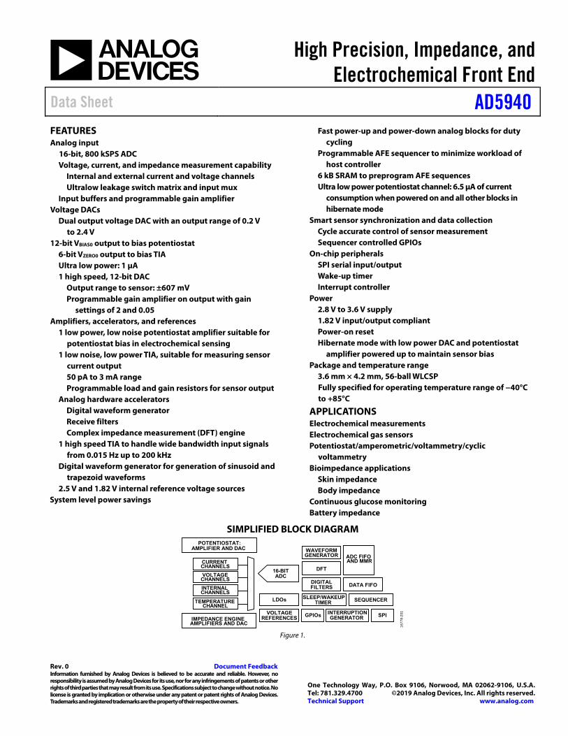
SIMPLIFIED BLOCK DIAGRAM
SPI
DATA FIFODIGITALFILTERS
DFT
SLEEP/WAKEUPTIMER
ADC FIFOAND MMR
SEQUENCER
WAVEFORMGENERATOR
INTERRUPTIONGENERATORGPIOs
POTENTIOSTAT:AMPLIFIER AND DAC
CURRENTCHANNELS
VOLTAGECHANNELS
INTERNALCHANNELS
TEMPERATURECHANNEL
16-BITADC
LDOs
VOLTAGEREFERENCESIMPEDANCE ENGINE
AMPLIFIERS AND DAC
1677
8-20
1
Figure 1.
AD5940 Data Sheet
Rev. 0 | Page 2 of 130
TABLE OF CONTENTS Features .............................................................................................. 1 Applications ....................................................................................... 1 Simplified Block Diagram ............................................................... 1 Revision History ............................................................................... 3 Functional Block Diagram .............................................................. 4 General Description ......................................................................... 5 Specifications ..................................................................................... 6
ADC RMS Noise Specifications ............................................... 15 SPI Timing Specifications ......................................................... 15
Absolute Maximum Ratings .......................................................... 17 Thermal Resistance .................................................................... 17 ESD Caution ................................................................................ 17
Pin Configuration and Function Descriptions ........................... 18 Typical Performance Characteristics ........................................... 20
Reference Test Circuit ................................................................ 22 Theory of Operation ...................................................................... 23
Configuration Registers ............................................................. 23 Silicon Identification ...................................................................... 26
Identification Registers .............................................................. 26 Low Power DAC ............................................................................. 27
Low Power DAC Switch Options ............................................. 27 Relationship Between the 12-Bit and 6-Bit Outputs .............. 29 Low Power DAC Use Cases ....................................................... 29 Low Power DAC Circuit Registers ........................................... 30
Low Power Potentiostat ................................................................. 33 Low Power TIA ............................................................................... 34
Low Power TIA Protection Diodes .......................................... 34 Using an External RTIA ............................................................... 34 Recommended Switch Settings for Various Operating Modes ........................................................................................... 34 Low Power TIA Circuits Registers ........................................... 37
High Speed DAC Circuits .............................................................. 40 High Speed DAC Output Signal Generation .......................... 40 Power Modes of the High Speed DAC Core ........................... 40 High Speed DAC Filter Options ............................................... 40 High Speed DAC Output Attenuation Options ..................... 41 High Speed DAC Excitation Amplifier ................................... 41 Coupling an AC Signal from the High Speed DAC to the DC Level Set by the Low Power DAC ............................................. 41
Avoiding Incoherency Errors Between Excitation and Measurement Frequencies During Impedance Measurements....................................................................................................... 41 High Speed DAC Calibration Options .................................... 42 High Speed DAC Circuit Registers .......................................... 43
High Speed TIA Circuits ............................................................... 46 High Speed TIA Configuration ................................................ 46 High Speed TIA Circuit Registers ............................................ 48
High Performance ADC Circuit ................................................... 50 ADC Circuit Overview .............................................................. 50 ADC Circuit Diagram ............................................................... 50 ADC Circuit Features ................................................................ 51 ADC Circuit Operation ............................................................. 51 ADC Transfer Function ............................................................. 51 ADC Low Power Current Input Channel ............................... 52 Selecting Inputs to ADC Mux .................................................. 52 ADC Postprocessing .................................................................. 52 Internal Temperature Sensor Channel .................................... 53 Sinc2 Filter (50 Hz/60 Hz Mains Filter) .................................. 53 ADC Calibration ........................................................................ 53 ADC Circuit Registers ............................................................... 54 ADC Calibration Registers ....................................................... 59 ADC Digital Postprocessing Registers (Optional) ................ 65 ADC Statistics Registers ............................................................ 66
Programmable Switch Matrix ....................................................... 68 Switch Descriptions ................................................................... 68 Recommended Configuration in Hibernate Mode ............... 68 Options for Controlling All Switches ...................................... 68 Programmable Switches Registers ........................................... 71
Precision Voltage References ........................................................ 81 High Power and Low Power Buffer Control Register—BUFSENCON ............................................................................. 81
Sequencer ........................................................................................ 83 Sequencer Features ..................................................................... 83 Sequencer Overview .................................................................. 83 Sequencer Commands ............................................................... 83 Sequencer Operation ................................................................. 85 Sequencer and FIFO Registers ................................................. 87
Waveform Generator...................................................................... 92 Waveform Generator Features .................................................. 92 Waveform Generator Operation .............................................. 92
Data Sheet AD5940
Rev. 0 | Page 3 of 130
Using the Waveform Generator with the Low Power DAC .. 92 Waveform Generator Registers ................................................. 93
SPI Interface ..................................................................................... 96 Overview ...................................................................................... 96 SPI Pins ......................................................................................... 96 SPI Operation .............................................................................. 96 Command Byte ............................................................................ 96 Writing to and Reading from Registers ................................... 96 Reading Data from the Data FIFO ........................................... 97
Sleep and Wake-Up Timer ............................................................. 98 Sleep and Wake-Up Timer Features ......................................... 98 Sleep and Wake-Up Timer Overview ....................................... 98 Configuring a Defined Sequence Order .................................. 98 Recommended Sleep and Wake-Up Timer Operation .......... 98 Sleep and Wake-Up Timer Registers ........................................ 99
Interrupts ....................................................................................... 103 Interrupt Controller Interupts ................................................ 103 Configuring the Interrupts ..................................................... 103 Custom Interrupts .................................................................... 103 External Interrupt Configuration .......................................... 103 Interrupt Registers ................................................................... 104 External Interrupt Configuration Registers ......................... 109
Digital Inputs/Outputs ................................................................ 113 Digital Inputs/Outputs Features ............................................. 113
Digital Inputs/Outputs Operation .......................................... 113 GPIO Registers .......................................................................... 114
System Resets ................................................................................. 117 Analog Die Reset Registers ...................................................... 117
Power Modes ................................................................................. 118 Active High Power Mode (>80 kHz) ...................................... 118 Active Low Power Mode (<80 kHz) ....................................... 118 Hibernate Mode ........................................................................ 118 Shutdown Mode ........................................................................ 118 Low Power Mode ...................................................................... 118 Power Modes Registers ............................................................ 118
Clocking Architecture .................................................................. 121 Clock Features ........................................................................... 121 Clock Architecture Registers ................................................... 121
Applications Information ............................................................. 125 EDA Bioimpedance Measurement Using a Low Bandwidth Loop ............................................................................................ 125 Body Impedance Analysis (BIA) Measurement Using a High Bandwidth Loop ........................................................................ 126 High Precision Potentiosat Configuration ............................ 127 Using the AD5940, AD8232, and AD8233 for Bioimpedance and Electrocardiogram (ECG) Measurements ..................... 128 Smart Water/Liquid Quality AFE ........................................... 129
Outline Dimensions ...................................................................... 130 Ordering Guide ......................................................................... 130
REVISION HISTORY 3/2019—Revision 0: Initial Version
AD5940 Data Sheet
Rev. 0 | Page 4 of 130
FUNCTIONAL BLOCK DIAGRAM
RC0_0
VBIAS0
RCAL0
RE0
AIN0
AIN6
16-BIT ADC160kSPS/400kSPS
AD5940
GAIN 1/1.5/2/4/9
MU
XTEMPERATURE
SENSOR
COARSE OFFSETCORRECTION
1.8V
+
–
EXCITATIONAMPLIFIER
LOOPPN
DACPDACN
12-BITVDAC
+HPTIA
VZERO
AAF
VZERO
COMMANDFIFO
DIGITALFILTERS
DFT
WAKE-UPTIMER
ADC FIFOAND MMR
SEQUENCER
WAVEFORMGENERATOR
INTERRUPTGENERATOR
32kHzOSC
16MHzOSC
DIGITAL
CLOCKGENERATOR
VREF_2V5/2
PG
A
RCF
VREF_1V82
VREF_1V82
AIN0AINx
VCE0VRE0
CRCGPIO
TRLOAD02
RLOAD03
SE0DE0
VBIAS
–
RTIA2
CE0
RE0
VBIAS
VREF_2V5
DUALOUTPUTS
12-BITVDAC
VBIAS
VZERO
+
–AMP
RE0
CE0
RC0_0 RC0_1
SE0
LPF0
HPBUF
REFBUF
LPBUF
0.92V INTERNALPRECISIONREFERENCE
0.92VLP REF
+LPTIA
VZERO
–
RTIA0
RTIA0
1.8V HPLDO
1.8V LPLDO
HIGH BANDWIDTH AFE LOOP
LOW BANDWIDTH AFE LOOP
POR
SPI
OSC16MHz/32MHzXTAL
DRIVER
GPIO0
MISOMOSISCLKCS
DNC
DNC
DNC
SW
ITC
H M
AT
RIX
XTALI XTALOVREF_1V82VREF_2V5 AGND_REFAVDDAVDD_REG
RESETDGND DVDD IOVDDDVD_REG_1V8
AIN4/LPF0
AGND
AFE1AFE2AFE3AFE4
VBIAS_CAP
AIN1AIN2
AIN3/BUF_VREF1V8
RC0_1RC0_2
VZERO0
SE0DE0
CE0
RCAL1
GPIO1GPIO2GPIO3GPIO4GPIO5GPIO6GPIO7
BUF PGA BUFAVDD/2
VDE0VZERO0VBIAS0
fC = 50kHz/100kHz/250kHz
1677
8-00
1
Figure 2.
Data Sheet AD5940
Rev. 0 | Page 5 of 130
GENERAL DESCRIPTION The AD5940 is a high precision, low power analog front end (AFE) designed for portable applications that require high precision, electrochemical-based measurement techniques, such as amper-ometric, voltammetric, or impedance measurements. The AD5940 is designed for skin impedance and body impedance measurements, and works with the AD8233 AFE in a complete bioelectric or biopotential measurement system. The AD5940 is designed for electrochemical toxic gas sensing.
The AD5940 consists of two high precision excitation loops and one common measurement channel, which enables a wide capability of measurements of the sensor under test. The first excitation loop consists of an ultra low power, dual output string, digital-to-analog converter (DAC), and a low power, low noise potentiostat. One output of the DAC controls the noninverting input of the potentiostat, and the other output controls the noninverting input of the transimpedance amplifier (TIA). This low power excitation loop is capable of generating signals from dc to 200 Hz.
The second excitation loop consists of a 12-bit DAC, referred to as the high speed DAC. This DAC is capable of generating high frequency excitation signals up to 200 kHz.
The AD5940 measurement channel features a 16-bit, 800 kSPS, multichannel successive approximation register (SAR) analog-to-digital converter (ADC) with input buffers, a built in antialias filter, and a programmable gain amplifier (PGA). An input mux in front of the ADC allows the user to select an input channel for measurement. These input channels include multiple external current inputs, external voltage inputs, and internal channels. The internal channels allow diagnostic measurements of the internal supply voltages, die temperature, and reference voltages.
The current inputs include two TIAs with programmable gain and load resistors for measuring different sensor types. The first TIA, referred to as the low power TIA, measures low bandwidth signals. The second TIA, referred to as the high speed TIA, measures high bandwidth signals up to 200 kHz.
An ultralow leakage, programmable switch matrix connects the sensor to the internal analog excitation and measurement blocks. This matrix provides an interface for connecting external RTIAs and calibration resistors. The matrix can also be used to multiplex multiple electronic measurement devices to the same wearable electrodes.
A precision 1.82 V and 2.5 V on-chip reference source is available. The internal ADC and DAC circuits use this on-chip reference source to ensure low drift performance for the 1.82 V and 2.5 V peripherals.
The AD5940 measurement blocks can be controlled via direct register writes through the serial peripheral interface (SPI) interface, or, alternatively, by using a preprogrammable sequencer, which provides autonomous control of the AFE chip. 6 kB of static random access memory (SRAM) is partitioned for a deep data first in, first out (FIFO) and command FIFO. Measurement commands are stored in the command FIFO and measurement results are stored in the data FIFO. A number of FIFO related interrupts are available to indicate when the FIFO is full.
A number of general-purpose inputs/outputs (GPIOs) are available and are controlled using the AFE sequencer, which allows cycle accurate control of multiple external sensor devices.
The AD5940 operates from a 2.8 V to 3.6 V supply and is specified over a temperature range of −40°C to +85°C. The AD5940 is packaged in a 56-lead, 3.6 mm × 4.2 mm WLCSP package.
AD5940 Data Sheet
Rev. 0 | Page 6 of 130
SPECIFICATIONS AVDD = DVDD = 2.8 V to 3.6 V; the maximum difference between supplies = 0.3 V; IOVDD = 1.8 V ± 10% and 2.8 V to 3.6 V; the ADC reference, excitation, DAC, and amplifier = 1.82 V, internal reference; low power DAC reference = 2.5 V, internal reference; TA = −40°C to +85°C, unless otherwise noted.
Table 1. Parameter Symbol Min Typ Max Unit Test Conditions/Comments BASIC ADC SPECIFICATIONS Pseudo differential mode measured relative to
ADC bias voltage (voltage on VBIAS_CAP pin, 1.11 V), unless otherwise noted; specifications based on high speed mode, unless otherwise noted; ADC voltage channel calibrated in production with PGA gain = 1.5; AFE die clock for the analog domain (ACLK) = 32 MHz or 16 MHz, unless otherwise noted
Data Rate1 fSAMPLE 400 kSPS High speed mode; decimation factor = 4 200 kSPS Normal mode; decimation factor = 4 Resolution1 16 Bits Number of data bits Integral Nonlinearity1 INL
Normal Mode −4 ±2.0 +4 LSB PGA gain = 1.5, 1.82 V internal reference, 1 LSB = 1.82 V ÷ 215 ÷ PGA gain
−5.6 ±2.0 +4.7 LSB PGA gain = 9, 1.82 V internal reference Differential Nonlinearity1 DNL
Normal Mode −0.99 ±0.9 +2.5 LSB PGA gain = 1.5, 1.82 V internal reference; 1 LSB = 1.82 V ÷ 215 ÷ PGA gain, no missing codes
DC Code Distribution2 ±6 LSB PGA gain = 1.5, low power mode, ADC input = 0.9 V; ADC output data rate = 200 kSPS; 1 LSB = 1.82 V ÷ 215
±6 LSB Input channel is low power TIA = 1 µA, RTIA = 512 kΩ, RLOAD = 10 Ω ADC output data rate = 200 kSPS
±6 LSB Input channel is high speed TIA = 1 µA, RTIA = 10 kΩ, RLOAD = 100 Ω ADC output data rate = 200 kSPS
ADC ENDPOINT ERRORS Offset Error
Low Power Mode −600 ±200 +600 µV PGA gain = 1.5, low power mode, all channels except AIN3
−620 ±200 +880 µV PGA gain = 1.5, AIN3 only High Power Mode1, 3 −1.1 ±0.5 +1.4 mV PGA gain = 1.5
Drift1 ±3 µV/°C Using 1.82 V internal reference Offset Matching ±2 LSB Matching compared to AIN3 Full-Scale Error −1000 ±400 +800 µV
PGA gain = 1.5, Excluding internal channels and AIN3; both negative and positive full scale; error at both endpoints
-1000 1000 µV PGA gain = 1.5. AIN3 only High Power Mode1,3 −2.2 ±0.9 +1.82 mV PGA gain = 1.5
Internal Channels 0.21 0.751 % of full-scale
AVDD/2, DVDD/2, VBIAS_CAP, VREF_2V5, VREF_1V82, AVDD_REG
Gain Drift1 −3 ±1 +3 µV/°C Full-scale error drift minus offset error drift Gain Error Matching ± 3 LSB Mismatch from channel to channel PGA Mismatch Error1 ADC offset and gain calibration with a gain
value of 1.5 PGA Gain = 1 to 1.5 −0.2 +0.1 +0.3 % PGA Gain =1.5 to 2 −0.2 +0.1 +0.3 % PGA Gain = 2 to 4 −0.3 +0.2 +0.8 % PGA Gain = 4 to 9 −0.55 +0.2 +0.55 %
Data Sheet AD5940
Rev. 0 | Page 7 of 130
Parameter Symbol Min Typ Max Unit Test Conditions/Comments ADC DYNAMIC PERFORMANCE fIN = 20 kHz sine wave, fSAMPLE = 200 kSPS; using
AINx voltage input channels; PGA gain = 1.5 Signal-to-Noise Ratio SNR Includes distortion and noise components
80 dB PGA gain = 1, 1.5, and 2 76 dB PGA gain = 4 70 dB PGA gain = 9
Total Harmonic Distortion1 THD −84 dB Peak Harmonic or Spurious Noise1 −86 dB Channel to Channel Crosstalk1 −86 dB Measured on adjacent channels Noise (RMS)4 See
Table 2 µV rms
800 nV/√Hz Chop on
400 nV/√Hz Chop off
ADC INPUT Input to ADC mux Input Voltage Ranges1 0.2 2.1 V Voltage applied to any input pin V Pseudo differential voltage between
VBIAS_CAP pin and analog input from ADC mux −0.9 +0.9 V Gain = 1 −0.9 +0.9 V Gain = 1.5 −0.6 +0.6 V Gain = 2 −0.3 +0.3 V Gain = 4 −0.133 +0.133 V Gain = 9 Input Current Range1 0.00005 3000 µA Low power TIA and high speed TIA current
input channel ranges Common Mode Range1 0.2 1.1 2.1 V Leakage Current −1.5 ±0.5 +1.5 nA AIN0, AIN1, AIN2, AIN3/BUF_VREF1V82,
AIN4/LPF0, AIN6, CE0, RE0 and SE0 ±2 DE0 pin only Input Current1 −8 ±2 +8 nA AIN0, AIN1, AIN2, AIN3, AIN4, AIN6, CE0, RE0,
SE0, and DE0 Input Capacitance 40 pF During ADC acquisition Antialias Filter 3 dB Frequency Range 3 programmable settings
Mode 0 50 kHz Mode 1 100 kHz Mode 2 250 kHz
ADC Channel Switch Settling Time Time delay required after switching ADC input channel; excludes sinc3 settling time
Antialias Filter −3 dB Cutoff Frequency
250 kHz1 20 µs 100 kHz1 40 µs 50 kHz1 60 µs
DISCRETE FOURIER TRANSFORM (DFT)-BASED IMPEDANCE MEASUREMENTS1
With High Bandwidth Loop For impedance (Z) of 1000 Ω (0.1% tolerant resistor), excitation frequency = 0.1 Hz to 200 kHz, sine amplitude = 10 mV rms, RTIA = 5 kΩ; RCAL = 200 Ω;1% accurate tempco 5 ppm/°C; single DFT measurement; DFT using 8192 ADC samples; Hanning on; HSDACCON, Bits[8:1] = 0x1B for low power mode and impedance measurements ≤80 kHz; HSDACCON, Bits[8:1] = 0x7 for high power mode and impedance measurements ≥80 kHz
Accuracy Magnitude −1.25 ±0.2 +1.25 % 20 kHz to 200 kHz ±0.2 % 10 Hz to 20 kHz ±1 % 1 Hz to <10 Hz
Phase −0.3 ±0.1 +0.3 Degrees
AD5940 Data Sheet
Rev. 0 | Page 8 of 130
Parameter Symbol Min Typ Max Unit Test Conditions/Comments Three-Resistor Star Cell
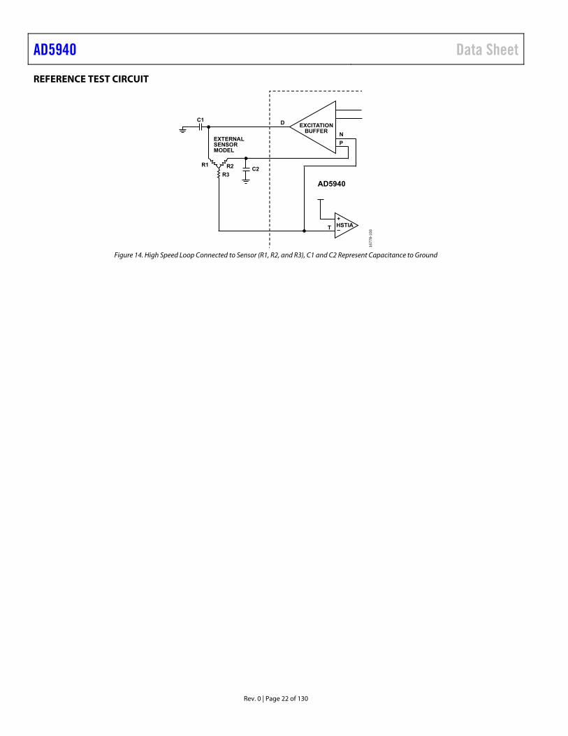
Accuracy R1 = R2 = R3 = 2.2 Ω (see Figure 14); 0.1 Hz to 200 kHz
Magnitude ±0.5 % Phase ±0.5 Degrees
Accuracy R1 = R2 = R3 = 100 Ω connected (see Figure 14); 0.1 kHz to 200 kHz
Magnitude ±0.2 % Phase ±0.2 Degrees
With High Bandwidth Loop, 50 kHz, 4-Wire Isolated
For Z = 1 kΩ (0.1% tolerant resistor); excitation frequency = 50 kHz; sine amplitude = 0.6 V p-p; RTIA = 1 kΩ; CTIA = 32 pF; Isolation Capacitor 1 (CISO1) = 15 nF; Isolation Capacitor 2 (CISO2) = Isolation Capacitor 3 (CISO3) = Isolation Capacitor 4 (CISO4) = 470 nF; current-limiting resistor (RLIMIT) = 1 kΩ
Accuracy Device to device repeatability for three devices at 50 kHz
Magnitude 0.26 % Percentage error Phase 1 Degrees
With Low Bandwidth Loop For Z = 100 kΩ; excitation frequency = 100 Hz; sine amplitude = 1.1 V p-p; RTIA = 100 kΩ; CTIA = 100 nF; CISO1 = 15 nF; CISO2 = 470 nF; RLIMIT = 1000 Ω
Frequency Range 1 300 Hz Accuracy Device to device repeatability for three devices
at 100 Hz Magnitude ±0.3 % Percentage error
Precision Magnitude 6.53 Ω Standard deviation
High Speed Loop See Figure 14; valid for impedance spectroscopy, voltammetry, and pulse tests
Allowed External Load Capacitance1
100 pF R2 + R3 ≤ 100 Ω; R1 ≤ 100 Ω
50 pF R2 + R3 ≤ 500 Ω; R1 ≤ 100 Ω 40 pF R2 + R3 ≤ 1600 Ω; R1 ≤ 800 Ω; frequency ≥ 1 kHz Excitation Amplifier Bandwidth 3 MHz Impedance Frequency Range 0.015 200000 Hz
LOW POWER TIA AND POTENTIOSTAT Input Bias Current1
TIA Amplifier, SE0 Pin 80 200 pA PA 20 150 pA
Offset Voltage1 50 150 μV Offset Voltage Drift vs. Temperature 1 μV/°C Noise Unity-gain mode; V p-p in 0.1 Hz to 10 Hz range 1.6 μV Normal mode (LPTIACON0, Bit 2 = 0) 2 μV Half power mode (LPTIACON0, Bit 2 = 1) Potentiostat Source/Sink Current1 −750 +750 μA Normal mode (LPTIACON0, Bits[4:3] = 00); from
CE0 −3 +3 mA High current mode (LPTIACON0, Bits[4:3] = 01
or 11 from CE0 DC PSRR 70 dB At RE0 pin; RTIA = 256 kΩ; RLOAD = 10 Ω Input Common-Mode Range1 300 AVDD –
600 mV
Output Voltage Range1 300 AVDD – 400
mV Normal mode (LPTIACON0, Bits[4:3] = 00; sink/source = 750 μA
300 AVDD − 400
mV High current mode (LPTIACON0, Bits[4:3] = 01 or 11); sink/source = 3 mA
Overcurrent Limit Protection 20 mA Amplifiers try to limit source/sink current to this value via internal clamp
Data Sheet AD5940
Rev. 0 | Page 9 of 130
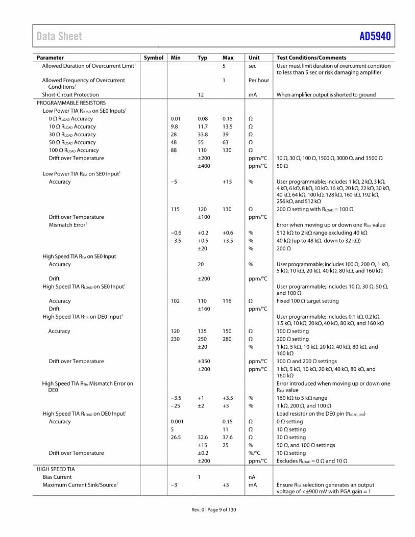
Parameter Symbol Min Typ Max Unit Test Conditions/Comments Allowed Duration of Overcurrent Limit1 5 sec User must limit duration of overcurrent condition
to less than 5 sec or risk damaging amplifier Allowed Frequency of Overcurrent
Conditions1 1 Per hour
Short-Circuit Protection 12 mA When amplifier output is shorted to ground
PROGRAMMABLE RESISTORS Low Power TIA RLOAD on SE0 Inputs1
0 Ω RLOAD Accuracy 0.01 0.08 0.15 Ω 10 Ω RLOAD Accuracy 9.8 11.7 13.5 Ω 30 Ω RLOAD Accuracy 28 33.8 39 Ω 50 Ω RLOAD Accuracy 48 55 63 Ω 100 Ω RLOAD Accuracy 88 110 130 Ω Drift over Temperature ±200 ppm/°C 10 Ω, 30 Ω, 100 Ω, 1500 Ω, 3000 Ω, and 3500 Ω ±400 ppm/°C 50 Ω
Low Power TIA RTIA on SE0 Input1 Accuracy −5 +15 % User programmable; includes 1 kΩ, 2 kΩ, 3 kΩ,
4 kΩ, 6 kΩ, 8 kΩ, 10 kΩ, 16 kΩ, 20 kΩ, 22 kΩ, 30 kΩ, 40 kΩ, 64 kΩ, 100 kΩ, 128 kΩ, 160 kΩ, 192 kΩ, 256 kΩ, and 512 kΩ
115 120 130 Ω 200 Ω setting with RLOAD = 100 Ω Drift over Temperature ±100 ppm/°C Mismatch Error1 Error when moving up or down one RTIA value −0.6 +0.2 +0.6 % 512 kΩ to 2 kΩ range excluding 40 kΩ −3.5 +0.5 +3.5 % 40 kΩ (up to 48 kΩ, down to 32 kΩ) ±20 % 200 Ω
High Speed TIA RTIA on SE0 Input Accuracy 20 % User programmable; includes 100 Ω, 200 Ω, 1 kΩ,
5 kΩ, 10 kΩ, 20 kΩ, 40 kΩ, 80 kΩ, and 160 kΩ Drift ±200 ppm/°C
High Speed TIA RLOAD on SE0 Input1 User programmable; includes 10 Ω, 30 Ω, 50 Ω, and 100 Ω
Accuracy 102 110 116 Ω Fixed 100 Ω target setting Drift ±160 ppm/°C
High Speed TIA RTIA on DE0 Input1 User programmable; includes 0.1 kΩ, 0.2 kΩ, 1.5 kΩ, 10 kΩ, 20 kΩ, 40 kΩ, 80 kΩ, and 160 kΩ
Accuracy 120 135 150 Ω 100 Ω setting 230 250 280 Ω 200 Ω setting
±20 % 1 kΩ, 5 kΩ, 10 kΩ, 20 kΩ, 40 kΩ, 80 kΩ, and 160 kΩ
Drift over Temperature ±350 ppm/°C 100 Ω and 200 Ω settings ±200 ppm/°C 1 kΩ, 5 kΩ, 10 kΩ, 20 kΩ, 40 kΩ, 80 kΩ, and
160 kΩ High Speed TIA RTIA Mismatch Error on
DE01 Error introduced when moving up or down one
RTIA value −3.5 +1 +3.5 % 160 kΩ to 5 kΩ range −25 ±2 +5 % 1 kΩ, 200 Ω, and 100 Ω
High Speed TIA RLOAD on DE0 Input1 Load resistor on the DE0 pin (RLOAD_DE0) Accuracy 0.001 0.15 Ω 0 Ω setting 5 11 Ω 10 Ω setting 26.5 32.6 37.6 Ω 30 Ω setting ±15 25 % 50 Ω, and 100 Ω settings Drift over Temperature ±0.2 %/°C 10 Ω setting
±200 ppm/°C Excludes RLOAD = 0 Ω and 10 Ω
HIGH SPEED TIA Bias Current 1 nA Maximum Current Sink/Source1 −3 +3 mA Ensure RTIA selection generates an output
voltage of <±900 mV with PGA gain = 1
AD5940 Data Sheet
Rev. 0 | Page 10 of 130
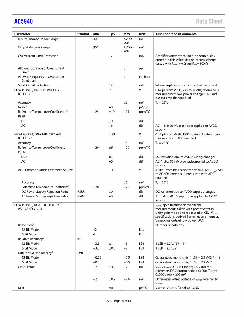
Parameter Symbol Min Typ Max Unit Test Conditions/Comments Input Common-Mode Range1 300 AVDD −
700 mV
Output Voltage Range1 200 AVDD − 400
mV
Overcurrent Limit Protection1 17 mA Amplifier attempts to limit the source/sink current to this value via the internal clamp; tested with RLOAD = 0 Ω and RTIA = 100 Ω
Allowed Duration of Overcurrent Limit1
5 sec
Allowed Frequency of Overcurrent Conditions
1 Per hour
Short-Circuit Protection 12 mA When amplifier output is shorted to ground
LOW POWER, ON-CHIP VOLTAGE REFERENCE
2.5 V 0.47 µF from VREF_2V5 to AGND; reference is measured with low power voltage DAC and output amplifier enabled
Accuracy ±5 mV TA = 25°C Noise1 60 µV p-p Reference Temperature Coefficient1, 8 −25 ±10 +25 ppm/°C PSRR
DC 70 dB AC5 48 dB AC 1 kHz; 50 mV p-p ripple applied to AVDD
supply
HIGH POWER, ON-CHIP VOLTAGE REFERENCE
1.82 V 0.47 µF from VREF_1V82 to AGND; reference is measured with ADC enabled
Accuracy ±5 mV TA = 25 °C Reference Temperature Coefficient1 −20 ±5 +20 ppm/°C PSRR
DC6 85 dB DC; variation due to AVDD supply changes AC 60 dB AC; 1 kHz, 50 mV p-p ripple applied to AVDD
supply ADC Common-Mode Reference Source 1.11 V 470 nF from bias capacitor on ADC (VBIAS_CAP)
to AGND; reference is measured with ADC enabled
Accuracy ±5 mV TA = 25°C Reference Temperature Coefficient1 −20 +20 ppm/°C DC Power Supply Rejection Ratio PSRR 80 dB DC variation due to AVDD supply changes AC Power Supply Rejection Ratio PSRR 60 dB AC 1 kHz, 50 mV p-p ripple applied to AVDD
supply
LOW POWER, DUAL OUTPUT DAC (VBIAS0 AND VZERO0)
VBIAS0 specifications derived from measurements taken with potentiostat in unity-gain mode and measured at CE0; VZERO0 specifications derived from measurements at VZERO0; dual output low power DAC
Resolution1 Number of data bits 12-Bit Mode 12 Bits 6-Bit Mode 6 Bits
Relative Accuracy1 INL 12-Bit Mode −3.5 ±1 +3 LSB 1 LSB = 2.2 V/(212 − 1) 6-Bit Mode −3.5 ±0.5 +2 LSB 1 LSB = 2.2 V/26
Differential Nonlinearity1 DNL 12-Bit Mode −0.99 +2.5 LSB Guaranteed monotonic, 1 LSB = 2.2 V/(212 − 1) 6-Bit Mode −0.5 +0.5 LSB Guaranteed monotonic, 1 LSB = 2.2 V/26
Offset Error1 −7 ±3.9 +7 mV VBIAS0/VZERO0 in 12-bit mode; 2.5 V internal reference, DAC output code = 0x000; Target 0x000 code = 200 mV
−2 ±0.2 +2.6 mV Differential offset voltage of VBIAS0 referred to VZERO0
Drift ±5 µV/°C VBIAS0 or VZERO0 referred to AGND
Data Sheet AD5940
Rev. 0 | Page 11 of 130
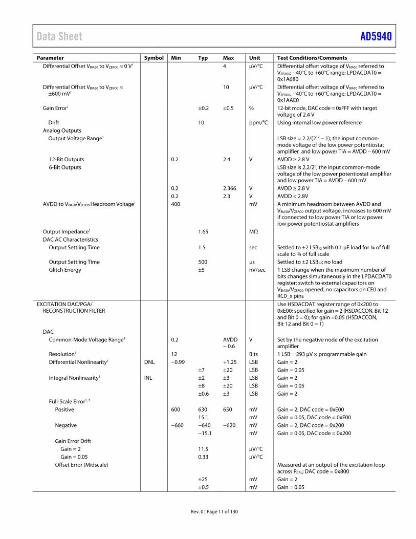
Parameter Symbol Min Typ Max Unit Test Conditions/CommentsDifferential Offset VBIAS0 to VZERO0 ≈ 0 V1 4 μV/°C Differential offset voltage of VBIAS0 referred to
VZERO0; −40°C to +60°C range; LPDACDAT0 = 0x1A680
Differential Offset VBIAS0 to VZERO0 ≈ ±600 mV1
10 μV/°C Differential offset voltage of VBIAS0 referred to VZERO0, −40°C to +60°C range; LPDACDAT0 = 0x1AAE0
Gain Error1 ±0.2 ±0.5 % 12-bit mode, DAC code = 0xFFF with target voltage of 2.4 V
Drift 10 ppm/°C Using internal low power reference Analog Outputs
Output Voltage Range1 LSB size = 2.2/(212 − 1); the input common-mode voltage of the low power potentiostat amplifier and low power TIA = AVDD – 600 mV
12-Bit Outputs 0.2 2.4 V AVDD ≥ 2.8 V 6-Bit Outputs LSB size is 2.2/26; the input common-mode
voltage of the low power potentiostat amplifier and low power TIA = AVDD – 600 mV
0.2 2.366 V AVDD ≥ 2.8 V 0.2 2.3 V AVDD < 2.8V
AVDD to VBIAS0/VZERO0 Headroom Voltage1 400 mV A minimum headroom between AVDD and VBIAS0/VZERO0 output voltage, increases to 600 mV if connected to low power TIA or low power low power potentiostat amplifiers
Output Impedance1 1.65 MΩDAC AC Characteristics
Output Settling Time 1.5 sec Settled to ±2 LSB12 with 0.1 μF load for ¼ of full scale to ¾ of full scale
Output Settling Time 500 μs Settled to ±2 LSB12; no load Glitch Energy ±5 nV/sec 1 LSB change when the maximum number of
bits changes simultaneously in the LPDACDAT0 register; switch to external capacitors on VBIAS0/VZERO0 opened; no capacitors on CE0 and RC0_x pins
EXCITATION DAC/PGA/ RECONSTRUCTION FILTER
Use HSDACDAT register range of 0x200 to 0xE00; specified for gain = 2 (HSDACCON, Bit 12 and Bit 0 = 0); for gain =0.05 (HSDACCON, Bit 12 and Bit 0 = 1)
DACCommon-Mode Voltage Range1 0.2 AVDD
− 0.6 V Set by the negative node of the excitation
amplifier Resolution1 12 Bits 1 LSB = 293 μV × programmable gain Differential Nonlinearity1 DNL −0.99 +1.25 LSB Gain = 2
±7 ±20 LSB Gain = 0.05 Integral Nonlinearity1 INL ±2 ±3 LSB Gain = 2
±8 ±20 LSB Gain = 0.05 ±0.6 ±3 LSB Gain = 2
Full-Scale Error1, 7
Positive 600 630 650 mV Gain = 2, DAC code = 0xE00 15.1 mV Gain = 0.05, DAC code = 0xE00
Negative −660 −640 −620 mV Gain = 2, DAC code = 0x200 −15.1 mV Gain = 0.05, DAC code = 0x200
Gain Error Drift Gain = 2 11.5 μV/°C Gain = 0.05 0.33 μV/°C
Offset Error (Midscale) Measured at an output of the excitation loop across RCAL; DAC code = 0x800
±25 mV Gain = 2 ±0.5 mV Gain = 0.05
AD5940 Data Sheet
Rev. 0 | Page 12 of 130
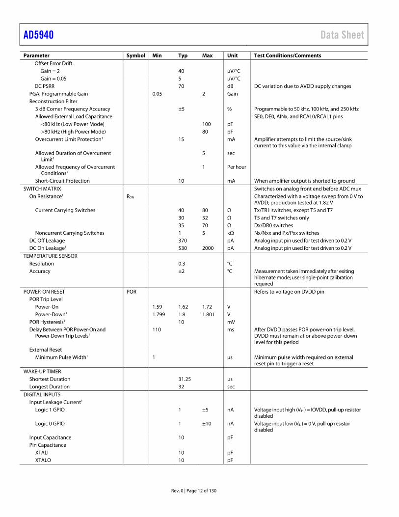
Parameter Symbol Min Typ Max Unit Test Conditions/Comments Offset Error Drift
Gain = 2 40 μV/°C Gain = 0.05 5 μV/°C
DC PSRR 70 dB DC variation due to AVDD supply changes PGA, Programmable Gain 0.05 2 Gain Reconstruction Filter
3 dB Corner Frequency Accuracy ±5 % Programmable to 50 kHz, 100 kHz, and 250 kHz Allowed External Load Capacitance SE0, DE0, AINx, and RCAL0/RCAL1 pins
<80 kHz (Low Power Mode) 100 pF >80 kHz (High Power Mode) 80 pF
Overcurrent Limit Protection1 15 mA Amplifier attempts to limit the source/sink current to this value via the internal clamp
Allowed Duration of Overcurrent Limit1
5 sec
Allowed Frequency of Overcurrent Conditions1
1 Per hour
Short-Circuit Protection 10 mA When amplifier output is shorted to ground
SWITCH MATRIX Switches on analog front end before ADC mux On Resistance1 RON Characterized with a voltage sweep from 0 V to
AVDD; production tested at 1.82 V Current Carrying Switches 40 80 Ω Tx/TR1 switches, except T5 and T7 30 52 Ω T5 and T7 switches only 35 70 Ω Dx/DR0 switches Noncurrent Carrying Switches 1 5 kΩ Nx/Nxx and Px/Pxx switches
DC Off Leakage 370 pA Analog input pin used for test driven to 0.2 V DC On Leakage1 530 2000 pA Analog input pin used for test driven to 0.2 V
TEMPERATURE SENSOR Resolution 0.3 °C Accuracy ±2 °C Measurement taken immediately after exiting
hibernate mode; user single-point calibration required
POWER-ON RESET POR Refers to voltage on DVDD pin POR Trip Level
Power-On 1.59 1.62 1.72 V Power-Down1 1.799 1.8 1.801 V
POR Hysteresis1 10 mV Delay Between POR Power-On and
Power-Down Trip Levels1 110 ms After DVDD passes POR power-on trip level,
DVDD must remain at or above power-down level for this period
External Reset Minimum Pulse Width1 1 μs Minimum pulse width required on external
reset pin to trigger a reset
WAKE-UP TIMER Shortest Duration 31.25 μs Longest Duration 32 sec
DIGITAL INPUTS Input Leakage Current1
Logic 1 GPIO 1 ±5 nA Voltage input high (VIH ) = IOVDD, pull-up resistor disabled
Logic 0 GPIO 1 ±10 nA Voltage input low (VIL ) = 0 V, pull-up resistor disabled
Input Capacitance 10 pF Pin Capacitance
XTALI 10 pF XTALO 10 pF
Data Sheet AD5940
Rev. 0 | Page 13 of 130
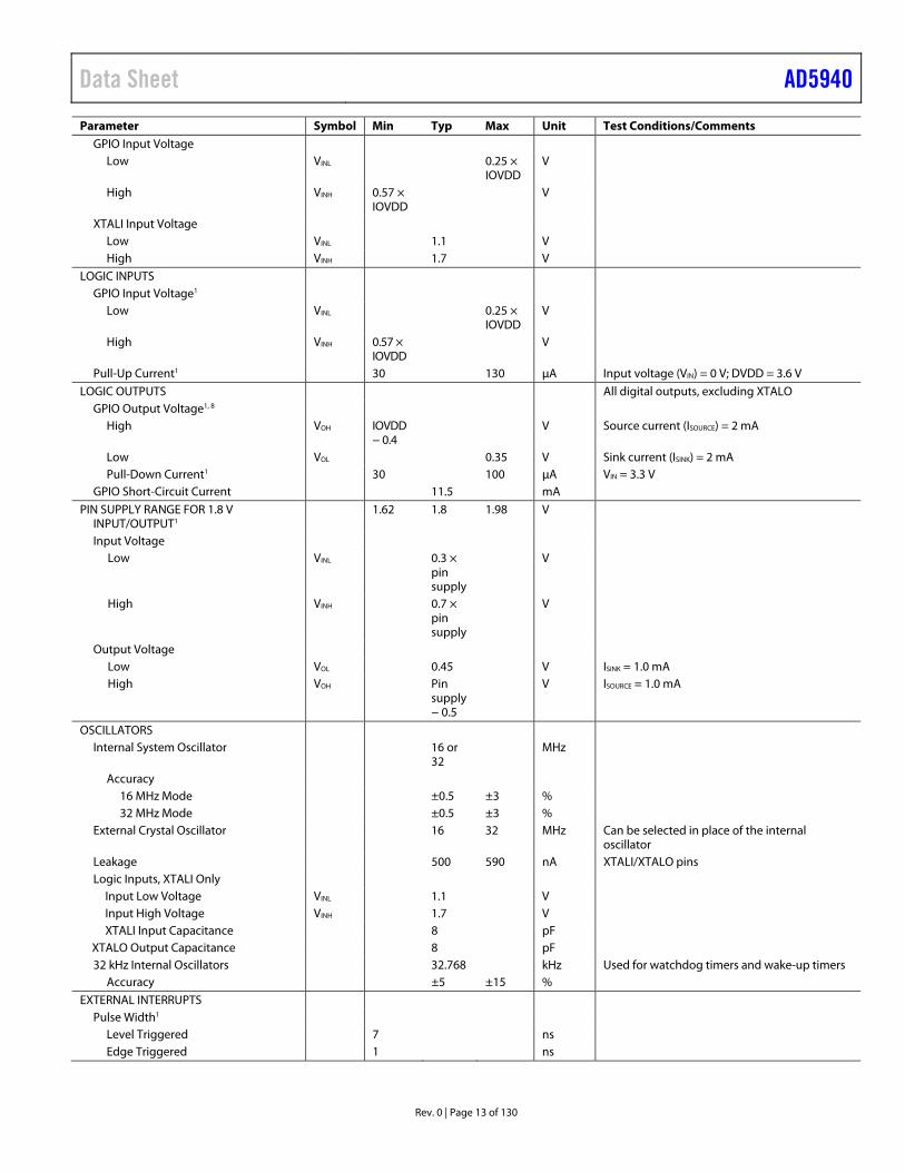
Parameter Symbol Min Typ Max Unit Test Conditions/CommentsGPIO Input Voltage
Low VINL 0.25 × IOVDD
V
High VINH 0.57 × IOVDD
V
XTALI Input Voltage Low VINL 1.1 V High VINH 1.7 V
LOGIC INPUTS GPIO Input Voltage1
Low VINL 0.25 × IOVDD
V
High VINH 0.57 × IOVDD
V
Pull-Up Current1 30 130 μA Input voltage (VIN) = 0 V; DVDD = 3.6 V
LOGIC OUTPUTS All digital outputs, excluding XTALO GPIO Output Voltage1, 8
High VOH IOVDD − 0.4
V Source current (ISOURCE) = 2 mA
Low VOL 0.35 V Sink current (ISINK) = 2 mA Pull-Down Current1 30 100 μA VIN = 3.3 V
GPIO Short-Circuit Current 11.5 mA
PIN SUPPLY RANGE FOR 1.8 V INPUT/OUTPUT1
1.62 1.8 1.98 V
Input Voltage Low VINL 0.3 ×
pin supply
V
High VINH 0.7 × pin supply
V
Output Voltage Low VOL 0.45 V ISINK = 1.0 mA High VOH Pin
supply − 0.5
V ISOURCE = 1.0 mA
OSCILLATORSInternal System Oscillator 16 or
32 MHz
Accuracy16 MHz Mode ±0.5 ±3 % 32 MHz Mode ±0.5 ±3 %
External Crystal Oscillator 16 32 MHz Can be selected in place of the internal oscillator
Leakage 500 590 nA XTALI/XTALO pinsLogic Inputs, XTALI Only
Input Low Voltage VINL 1.1 V Input High Voltage VINH 1.7 V XTALI Input Capacitance 8 pF
XTALO Output Capacitance 8 pF 32 kHz Internal Oscillators 32.768 kHz Used for watchdog timers and wake-up timers
Accuracy ±5 ±15 %
EXTERNAL INTERRUPTS Pulse Width1
Level Triggered 7 ns Edge Triggered 1 ns
AD5940 Data Sheet
Rev. 0 | Page 14 of 130
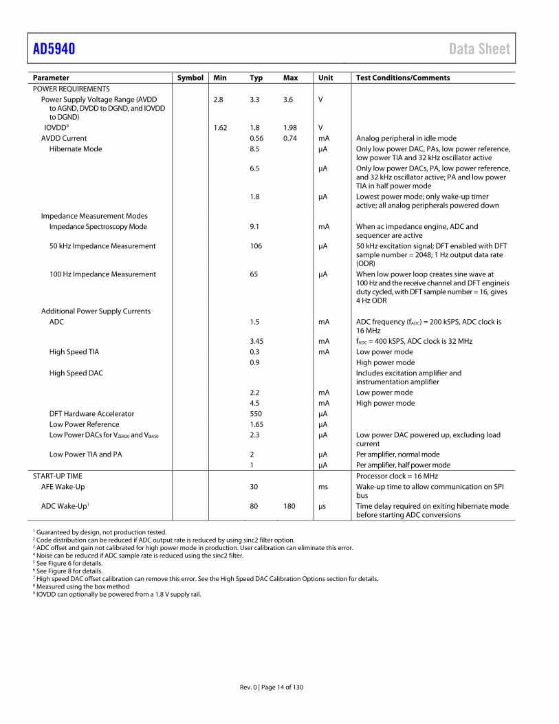
Parameter Symbol Min Typ Max Unit Test Conditions/Comments POWER REQUIREMENTS
Power Supply Voltage Range (AVDD to AGND, DVDD to DGND, and IOVDD to DGND)
2.8 3.3 3.6 V
IOVDD9 1.62 1.8 1.98 V AVDD Current 0.56 0.74 mA Analog peripheral in idle mode
Hibernate Mode 8.5 μA Only low power DAC, PAs, low power reference, low power TIA and 32 kHz oscillator active
6.5 μA Only low power DACs, PA, low power reference, and 32 kHz oscillator active; PA and low power TIA in half power mode
1.8 μA Lowest power mode; only wake-up timer active; all analog peripherals powered down
Impedance Measurement Modes Impedance Spectroscopy Mode 9.1 mA When ac impedance engine, ADC and
sequencer are active 50 kHz Impedance Measurement 106 μA 50 kHz excitation signal; DFT enabled with DFT
sample number = 2048; 1 Hz output data rate (ODR)
100 Hz Impedance Measurement 65 μA When low power loop creates sine wave at 100 Hz and the receive channel and DFT engineis duty cycled, with DFT sample number = 16, gives 4 Hz ODR
Additional Power Supply Currents ADC 1.5 mA ADC frequency (fADC) = 200 kSPS, ADC clock is
16 MHz 3.45 mA fADC = 400 kSPS, ADC clock is 32 MHz High Speed TIA 0.3 mA Low power mode 0.9 High power mode High Speed DAC Includes excitation amplifier and
instrumentation amplifier 2.2 mA Low power mode 4.5 mA High power mode DFT Hardware Accelerator 550 μA Low Power Reference 1.65 μA Low Power DACs for VZERO0 and VBIAS0 2.3 μA Low power DAC powered up, excluding load
current Low Power TIA and PA 2 μA Per amplifier, normal mode 1 μA Per amplifier, half power mode
START-UP TIME Processor clock = 16 MHz AFE Wake-Up 30 ms Wake-up time to allow communication on SPI
bus ADC Wake-Up1 80 180 μs Time delay required on exiting hibernate mode
before starting ADC conversions 1 Guaranteed by design, not production tested. 2 Code distribution can be reduced if ADC output rate is reduced by using sinc2 filter option. 3 ADC offset and gain not calibrated for high power mode in production. User calibration can eliminate this error. 4 Noise can be reduced if ADC sample rate is reduced using the sinc2 filter. 5 See Figure 6 for details. 6 See Figure 8 for details. 7 High speed DAC offset calibration can remove this error. See the High Speed DAC Calibration Options section for details. 8 Measured using the box method 9 IOVDD can optionally be powered from a 1.8 V supply rail.
Data Sheet AD5940
Rev. 0 | Page 15 of 130
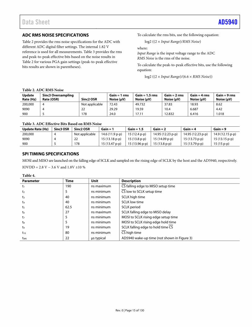
ADC RMS NOISE SPECIFICATIONS Table 2 provides the rms noise specifications for the ADC with different ADC digital filter settings. The internal 1.82 V reference is used for all measurements. Table 3 provides the rms and peak-to-peak effective bits based on the noise results in Table 2 for various PGA gain settings (peak-to-peak effective bits results are shown in parentheses).
To calculate the rms bits, use the following equation:
log2 ((2 × Input Range)/RMS Noise)
where: Input Range is the input voltage range to the ADC RMS Noise is the rms of the noise.
To calculate the peak-to-peak effective bits, use the following equation:
log2 ((2 × Input Range)/(6.6 × RMS Noise))
Table 2. ADC RMS Noise Update Rate (Hz)
Sinc3 Oversampling Rate (OSR) Sinc2 OSR
Gain = 1 rms Noise (μV)
Gain = 1.5 rms Noise (μV)
Gain = 2 rms Noise (μV)
Gain = 4 rms Noise (μV)
Gain = 9 rms Noise (μV)
200,000 4 Not applicable 72.43 49.732 37.83 18.93 8.62 9090 4 22 29.29 19.59 10.4 6.687 4.42 900 5 178 24.0 17.11 12.832 6.416 1.018
Table 3. ADC Effective Bits Based on RMS Noise Update Rate (Hz) Sinc3 OSR Sinc2 OSR Gain = 1 Gain = 1.5 Gain = 2 Gain = 4 Gain = 9 200,000 4 Not applicable 14.6 (11.9 p-p) 15 (12.4 p-p) 14.95 (12.23 p-p) 14.95 (12.23 p-p) 14.9 (12.15 p-p) 9090 4 22 15 (13.18 p-p) 15 (13.8 p-p) 15 (14.09 p-p) 15 (13.73 p-p) 15 (13.15 p-p) 900 5 178 15 (13.47 p-p) 15 (13.96 p-p) 15 (13.8 p-p) 15 (13.79 p-p) 15 (15 p-p)
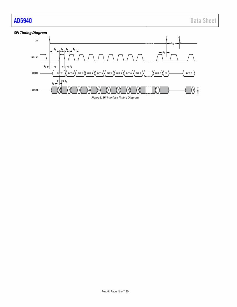
SPI TIMING SPECIFICATIONS MOSI and MISO are launched on the falling edge of SCLK and sampled on the rising edge of SCLK by the host and the AD5940, respectively.
IOVDD = 2.8 V − 3.6 V and 1.8V ±10 %
Table 4. Parameter Time Unit Description t1 190 ns maximum CS falling edge to MISO setup time
t2 5 ns minimum CS low to SCLK setup time
t3 40 ns minimum SCLK high time t4 40 ns minimum SCLK low time t5 62.5 ns minimum SCLK period t6 27 ns maximum SCLK falling edge to MISO delay t7 5 ns minimum MOSI to SCLK rising edge setup time t8 5 ns minimum MOSI to SCLK rising edge hold time t9 19 ns minimum SCLK falling edge to hold time CS
t10 80 ns minimum CS high time
tWK 22 μs typical AD5940 wake-up time (not shown in Figure 3)
AD5940 Data Sheet
Rev. 0 | Page 16 of 130
SPI Timing Diagram
t4t3t2
t1 t6
t7
t8
t5
t10
SCLK
MISO
MOSI 7 76 5 4 3 2 1 0 7
BIT 7 BIT 6 BIT 5 BIT 4 BIT 3 BIT 2 BIT 1 BIT 0 BIT 7 BIT 0 X BIT 7
CS
1677
8-00
3
t9
Figure 3. SPI Interface Timing Diagram
Data Sheet AD5940
Rev. 0 | Page 17 of 130
ABSOLUTE MAXIMUM RATINGS Table 5. Parameter Rating AVDD to AGND −0.3 V to +3.6 V DVDD to DGND −0.3 V to +3.6 V IOVDD to DGND −0.3 V to +3.6 V Analog Input Voltage to AGND −0.3 V to AVDD +0.3V Digital Input Voltage to DGND −0.3 V to DVDD +0.3V Digital Output Voltage to DGND −0.3 V to DVDD +0.3V AGND to DGND −0.3 V to +0.3 V Total GPIOx Pins Current
Positive 0 mA to 30 mA Negative −30 mA to 0 mA
Storage Temperature Range −65°C to +150°C Operating Temperature Range −40°C to +85°C Reflow Profile
Moisture Sensitivity Level 3 (MSL3) J-STD 020E (JEDEC) Junction Temperature 150°C Electrostatic Discharge (ESD)
Human Body Model (HBM) 2 kV Field Induced Charged Device
Model (FICDM) 1 kV
Machine Model (MM) 100 V
Stresses at or above those listed under Absolute Maximum Ratings may cause permanent damage to the product. This is a stress rating only; functional operation of the product at these or any other conditions above those indicated in the operational section of this specification is not implied. Operation beyond the maximum operating conditions for extended periods may affect product reliability.
THERMAL RESISTANCE Thermal performance is directly linked to printed circuit board (PCB) design and operating environment. Close attention to PCB thermal design is required.
θJA is the natural convection junction to ambient thermal resistance measured in a one cubic foot sealed enclosure.
θJC is the junction to case thermal resistance.
Table 6. Thermal Resistance1 Package Type θJA θJC Unit CB-56-3 33.0702 0.0642 °C/W
1 Thermal impedance simulated values are based on a JEDEC 2S2P thermal test board. See
JEDEC JESD51.
ESD CAUTION
AD5940 Data Sheet
Rev. 0 | Page 18 of 130
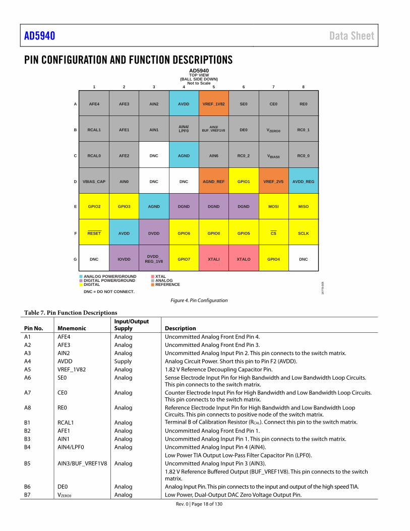
PIN CONFIGURATION AND FUNCTION DESCRIPTIONS
1
A
B
C
D
E
F
G
2 3 4 5 6 7
AFE4 AFE3 AIN2 AVDD VREF_1V82 SE0 CE0 RE0
RCAL1 AFE1 AIN1AIN4/LPF0
AIN3/BUF_VREF1V8 DE0 VZERO0 RC0_1
RCAL0 AFE2 DNC AIN6 RC0_2 VBIAS0 RC0_0
VBIAS_CAP AIN0 DNC DNC AGND_REF GPIO1 VREF_2V5 AVDD_REG
GPIO2 GPIO3 AGND DGND DGND DGND MOSI MISO
RESET AVDD DVDD GPIO6 GPIO0 GPIO5 CS SCLK
DNC IOVDDDVDD_
REG_1V8 GPIO7 XTALI XTALO GPIO4 DNC
8
ANALOG POWER/GROUNDDIGITAL POWER/GROUNDDIGITAL
DNC = DO NOT CONNECT.
AD5940TOP VIEW
(BALL SIDE DOWN)Not to Scale
XTALANALOGREFERENCE
AGND
1677
8-00
5
Figure 4. Pin Configuration
Table 7. Pin Function Descriptions
Pin No. Mnemonic Input/Output Supply Description
A1 AFE4 Analog Uncommitted Analog Front End Pin 4. A2 AFE3 Analog Uncommitted Analog Front End Pin 3. A3 AIN2 Analog Uncommitted Analog Input Pin 2. This pin connects to the switch matrix. A4 AVDD Supply Analog Circuit Power. Short this pin to Pin F2 (AVDD). A5 VREF_1V82 Analog 1.82 V Reference Decoupling Capacitor Pin. A6 SE0 Analog Sense Electrode Input Pin for High Bandwidth and Low Bandwidth Loop Circuits.
This pin connects to the switch matrix. A7 CE0 Analog Counter Electrode Input Pin for High Bandwidth and Low Bandwidth Loop Circuits.
This pin connects to the switch matrix. A8 RE0 Analog Reference Electrode Input Pin for High Bandwidth and Low Bandwidth Loop
Circuits. This pin connects to positive node of the switch matrix. B1 RCAL1 Analog Terminal B of Calibration Resistor (RCAL). Connect this pin to the switch matrix.
B2 AFE1 Analog Uncommitted Analog Front End Pin 1. B3 AIN1 Analog Uncommitted Analog Input Pin 1. This pin connects to the switch matrix. B4 AIN4/LPF0 Analog Uncommitted Analog Input Pin 4 (AIN4). Low Power TIA Output Low-Pass Filter Capacitor Pin (LPF0). B5 AIN3/BUF_VREF1V8 Analog Uncommitted Analog Input Pin 3 (AIN3). 1.82 V Reference Buffered Output (BUF_VREF1V8). This pin connects to the switch
matrix. B6 DE0 Analog Analog Input Pin. This pin connects to the input and output of the high speed TIA. B7 VZERO0 Analog Low Power, Dual-Output DAC Zero Voltage Output Pin.
Data Sheet AD5940
Rev. 0 | Page 19 of 130
Pin No. Mnemonic Input/Output Supply Description
B8 RC0_1 Analog Low Power TIA Reconstruction Filter 0 Feedback Pin 1. This pin is connected to the output of the low power TIA.
C1 RCAL0 Analog Terminal A of Calibration Resistor. Connect this pin to the switch matrix. C2 AFE2 Analog Uncommitted Analog Front End Pin 2. C3, D3 DNC Analog Do Not Connect. Do not connect to this pin. C4 AGND Ground Analog Ground. Short this pin to Pin E3 (AGND). C5 AIN6 Analog Uncommitted Analog Input Pin 6. C6 RC0_2 Analog Low Power TIA Reconstruction Filter 0 Pin 2. This pin can be left open (optional). C7 VBIAS0 Analog Low Power, Dual-Output DAC Bias Voltage Output Pin. C8 RC0_0 Analog Low Power TIA Feedback Pin. This pin is connected to the feedback of the low
power TIA. D1 VBIAS_CAP Analog VBIAS0 Decoupling Capacitor Pin. D2 AIN0 Analog Uncommitted Analog Input Pin 0. This pin connects to the switch matrix. D4, G1, G8 DNC Not applicable Do Not Connect. Do not connect to this pin. D5 AGND_REF Ground Analog Reference Ground. D6 GPIO1 Digital
input/output General-Purpose Input/Output Pin 1.
D7 VREF_2V5 Analog 2.5 V Analog Reference Decoupling Capacitor Pin. D8 AVDD_REG Supply Analog Regulator Decoupling Capacitor Pin. E1 GPIO2 Digital
input/output General-Purpose Input/Output Pin 2.
E2 GPIO3 Digital input/output
General-Purpose Input/Output Pin 3.
E3 AGND Ground Analog Ground. Short this pin to Pin C4. E4 to E6 DGND Ground Digital Ground E7 MOSI Digital input SPI Master Output, Slave Input. E8 MISO Digital output SPI Master Input Slave Output. F1 RESET Digital input Reset Pin, Active Low.
F2 AVDD Supply Analog 3.3 V Circuit Power. F3 DVDD Supply Digital Circuit Power. F4 GPIO6 Digital
input/output General-Purpose Input/Output Pin 6.
F5 GPIO0 Digital input/output
General-Purpose Input/Output Pin 0.
F6 GPIO5 Digital input/output
General-Purpose Input/Output Pin 5.
F7 CS Digital input/output
SPI Chip Select.
F8 SCLK Digital input SPI Clock. G2 IOVDD Supply Digital Input/Output Supply Pin. DVDD (Pin F3) must be driven before IOVDD is enabled. G3 DVDD_REG_1V8 Analog 1.8 V Digital Regulator Decoupling Capacitor Pin. G4 GPIO7 Digital
input/output General-Purpose Input/Output Pin 7.
G5 XTALI Digital Input 16 MHz External Crystal Input Pin. G6 XTALO Digital Output 16 MHz External Crystal Output Pin. G7 GPIO4 Digital
input/output General-Purpose Input/Output Pin 4.
AD5940 Data Sheet
Rev. 0 | Page 20 of 130
TYPICAL PERFORMANCE CHARACTERISTICS 0
–100
FREQUENCY (Hz)10 100 1k 10k 100k 1M 10M
MAG
NITU
DE(d
B)
–10
–20
–30
–40
–50
–60
–70
–80
–90
1677
8-20
6
Figure 5. Magnitude vs. Frequency, ADC 1.82 V Voltage Reference AC PSRR
0
–10010 100 1k 10k
FREQUENCY (Hz)100k 1M 10M
MA
GN
ITU
DE
(dB
)
–10
–20
–30
–40
–50
–60
–70
–80
–90
1677
8-20
7
Figure 6. Magnitude vs. Frequency, Low Power 2.5 V Voltage Reference
AC PSRR
2.499762.499742.499722.499702.49968
2.499642.49966
2.499622.499602.499582.499562.499542.499522.499502.499482.49946
2.7 2.8 2.9 3.0 3.1 3.2 3.3 3.4 3.5 3.6
LOW
PO
WER
REF
EREN
CE
(V)
SUPPLY VOLTAGE (V) 1677
8-20
8
Figure 7. Low Power Reference (2.5 V) vs. Supply Voltage, DC PSRR
2.7 2.8 2.9 3.0 3.1 3.2 3.3 3.4 3.5 3.6SUPPLY VOLTAGE (V)
1.1105301.1105281.1105261.1105241.1105221.1105201.1105181.1105161.1105141.1105121.1105101.1105081.1105061.1105041.1105021.1105001.1104981.110496
HIG
H P
OW
ER R
EFER
ENC
E(V
)
1677
8-20
9
Figure 8. High Power Reference vs. Supply Voltage, 1.11 V Voltage Reference DC PSRR
2.7 2.8 2.9 3.0 3.1 3.2 3.3 3.4 3.5 3.6SUPPLY VOLTAGE (V)
1.8209501.8209481.8209461.8209441.8209421.8209401.8209381.8209361.8209341.8209321.8209301.8209281.8209261.8209241.820922
HIG
H P
OW
ER R
EFER
ENC
E(V
)
1677
8-21
0
Figure 9. High Power Reference vs. Supply Voltage, ADC 1.82 V Voltage Reference DC PSRR
6
–2
0
3
5
2
–1
1
4
LOW
PO
WER
PO
TEN
TIO
STAT
INPU
T B
IAS
CU
RR
ENT
(I BIA
S)(p
A)
RE0 PIN VOLTAGE (V)0.2 0.4 0.6 0.8 2.0 2.21.0 1.2 1.4 1.6 1.8 2.4
1677
8-21
1
Figure 10. Low Power Potentiostat Input Bias Current (IBIAS) vs. RE0 Pin
Voltage
Data Sheet AD5940
Rev. 0 | Page 21 of 130
40
–140
–100
–60
–20
20
–120
–80
–40
0
–40 25 60 85
LOW
PO
WER
TIA
INPU
T B
IAS
CU
RR
ENT
(pA
)
TEMPERATURE (°C)
SE0 = 200mVSE0 = 1100mVSE0 = 2100mV
1677
8-21
2
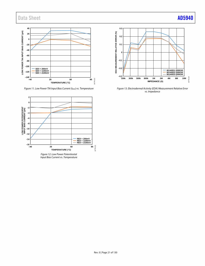
Figure 11. Low Power TIA Input Bias Current (IBIAS) vs. Temperature
2
–16
–12
–8
–4
0
–14
–10
–6
–2
LOW
PO
WER
PO
TENT
IOST
ATIN
PUT
BIAS
CUR
RENT
(pA)
TEMPERATURE (°C)
RE0 = 200mVRE0 = 1100mVRE0 = 2100mV
–40 25 60 85
1677
8-21
3
Figure 12. Low Power Potentiostat Input Bias Current vs. Temperature
0.3
–0.3
–0.1
0.1
–0.2
0
0.2
EDA
MEA
SURE
MEN
T RE
LATI
VE E
RRO
R (%
)
IMPEDANCE (Ω)
BOARD1 ERRORBOARD2 ERRORBOARD3 ERROR
100k 300k 500k 800k 1M 2M 4M 8M 10M
1677
8-21
4
Figure 13. Electrodermal Activity (EDA) Measurement Relative Error vs. Impedance
AD5940 Data Sheet
Rev. 0 | Page 22 of 130
REFERENCE TEST CIRCUIT
EXCITATIONBUFFER
+HSTIAT
AD5940
–
D
P
N
C2
C1
R2
EXTERNALSENSORMODEL
R3
R1
1677
8-10
3
Figure 14. High Speed Loop Connected to Sensor (R1, R2, and R3), C1 and C2 Represent Capacitance to Ground
Data Sheet AD5940
Rev. 0 | Page 23 of 130
THEORY OF OPERATION The main blocks of the AD5940 are as follows:
• Low power, dual-output, string DAC used to set the sensor bias voltage and low frequency excitation. Supports chronoamperometric and voltammetry electrochemical techniques.
• Low power potentiostat that applies the bias voltage to the sensor.
• Low power TIA that performs low bandwidth current measurements.
• High speed DAC and amplifier designed to generate excitation signals for impedance measurements up to 200 kHz.
• High speed TIA that supports wider signal bandwidth measurements.
• High performance ADC circuit (see the High Performance ADC Circuit section).
• Programmable switch matrix. The input switching of the AD5940 allows full configurability in the connections of the external sensors (see the Programmable Switch Matrix section).
• Programmable sequencer (see the Sequencer section). • SPI interface. • Waveform generator designed to create sinusoid and
trapezoid waveforms up to 200 kHz (see the Waveform Generator section).
• Interrupt sources that output to a GPIOx pin to alert the host controller that an interrupt event occurred (see the Interrupts).
• Digital inputs/outputs (see the Digital Inputs/Outputs section).
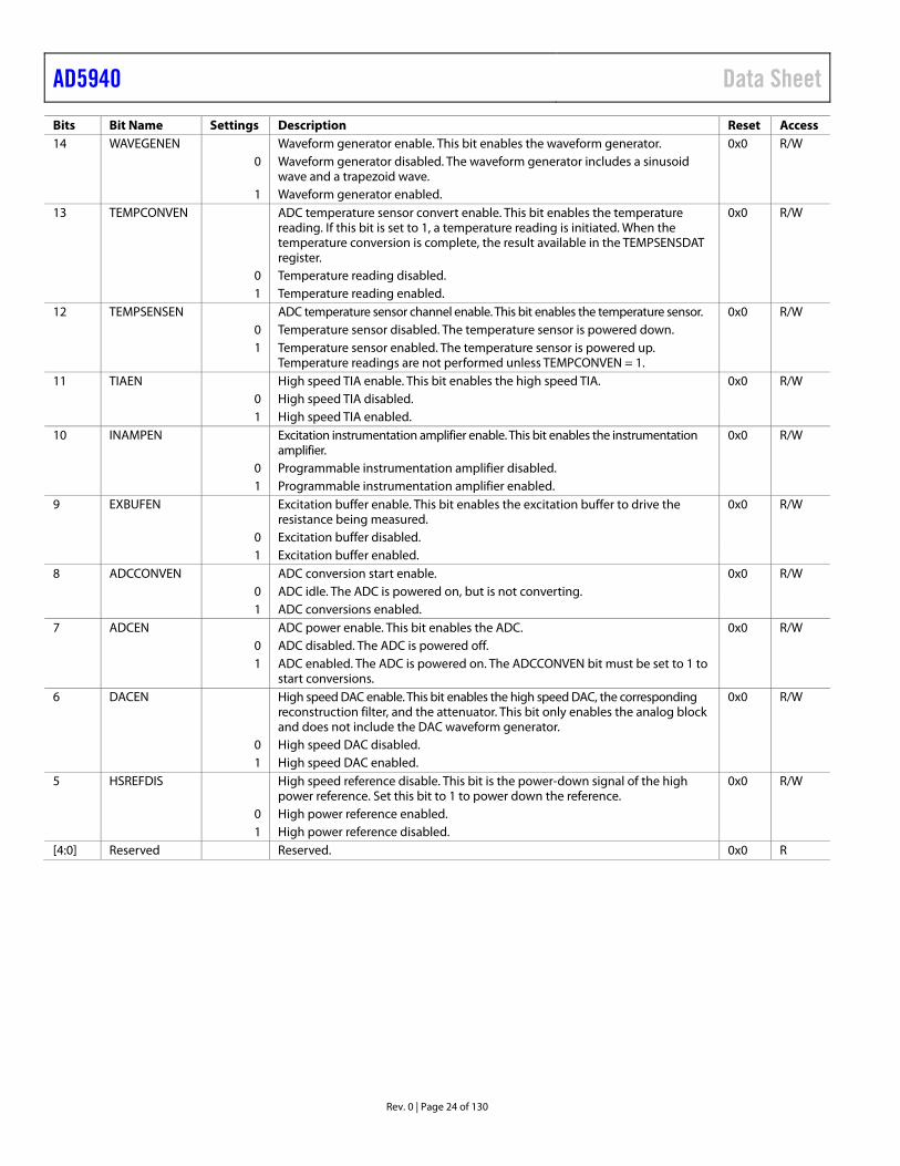
CONFIGURATION REGISTERS
Table 8. Configuration Registers Summary Address Name Description Reset Access 0x00002000 AFECON AFE configuration register 0x00080000 R/W 0x000022F0 PMBW Power modes configuration register 0x00088800 R/W
Configuration Register—AFECON
Address 0x00002000, Reset: 0x00080000, Name: AFECON
Table 9. Bit Descriptions for AFECON Register Bits Bit Name Settings Description Reset Access [31:22] Reserved Reserved. 0x0 R 21 DACBUFEN Enables the dc DAC buffer. This bit enables the buffer for the high impedance
output of the dc DAC. 0x0 R/W
0 Disables the dc DAC buffer. 1 Enables the dc DAC buffer. 20 DACREFEN High speed DAC reference enable. 0x0 R/W 0 Reference disable. Clear to 0 to disable the high speed DAC reference. 1 Reference enable. Set to 1 to enable the high speed DAC reference. 19 ALDOILIMITEN Analog low dropout (LDO) regulator current limiting. This bit enables AFE
analog LDO buffer current limiting. If enabled, this feature limits the current drawn from the battery while charging the capacitor on the AVDD_REG pin.
0x1 R/W
0 Analog LDO buffer current limiting enabled. 1 Analog LDO buffer current limiting disabled. [18:17] Reserved Reserved. 0x0 R 16 SINC2EN ADC output 50 Hz/60 Hz filter enable. This bit enables the 50 Hz/60 Hz supply
rejection filter. 0x0 R/W
0 Supply rejection filter disabled. Disables sinc2 (50 Hz/60 Hz digital filter). Disable this bit for impedance measurements.
1 Supply rejection filter enabled. Enables sinc2 (50 Hz/60 Hz digital filter). 15 DFTEN DFT hardware accelerator enable. This bit enables the DFT hardware
acceleration block. 0x0 R/W
0 DFT hardware accelerator disabled. 1 DFT hardware accelerator enabled.
AD5940 Data Sheet
Rev. 0 | Page 24 of 130
Bits Bit Name Settings Description Reset Access 14 WAVEGENEN Waveform generator enable. This bit enables the waveform generator. 0x0 R/W 0 Waveform generator disabled. The waveform generator includes a sinusoid
wave and a trapezoid wave.
1 Waveform generator enabled. 13 TEMPCONVEN ADC temperature sensor convert enable. This bit enables the temperature
reading. If this bit is set to 1, a temperature reading is initiated. When the temperature conversion is complete, the result available in the TEMPSENSDAT register.
0x0 R/W
0 Temperature reading disabled. 1 Temperature reading enabled. 12 TEMPSENSEN ADC temperature sensor channel enable. This bit enables the temperature sensor. 0x0 R/W 0 Temperature sensor disabled. The temperature sensor is powered down. 1 Temperature sensor enabled. The temperature sensor is powered up.
Temperature readings are not performed unless TEMPCONVEN = 1.
11 TIAEN High speed TIA enable. This bit enables the high speed TIA. 0x0 R/W 0 High speed TIA disabled. 1 High speed TIA enabled. 10 INAMPEN Excitation instrumentation amplifier enable. This bit enables the instrumentation
amplifier. 0x0 R/W
0 Programmable instrumentation amplifier disabled. 1 Programmable instrumentation amplifier enabled. 9 EXBUFEN Excitation buffer enable. This bit enables the excitation buffer to drive the
resistance being measured. 0x0 R/W
0 Excitation buffer disabled. 1 Excitation buffer enabled. 8 ADCCONVEN ADC conversion start enable. 0x0 R/W 0 ADC idle. The ADC is powered on, but is not converting. 1 ADC conversions enabled. 7 ADCEN ADC power enable. This bit enables the ADC. 0x0 R/W 0 ADC disabled. The ADC is powered off. 1 ADC enabled. The ADC is powered on. The ADCCONVEN bit must be set to 1 to
start conversions.
6 DACEN High speed DAC enable. This bit enables the high speed DAC, the corresponding reconstruction filter, and the attenuator. This bit only enables the analog block and does not include the DAC waveform generator.
0x0 R/W
0 High speed DAC disabled. 1 High speed DAC enabled. 5 HSREFDIS High speed reference disable. This bit is the power-down signal of the high
power reference. Set this bit to 1 to power down the reference. 0x0 R/W
0 High power reference enabled. 1 High power reference disabled. [4:0] Reserved Reserved. 0x0 R
Data Sheet AD5940
Rev. 0 | Page 25 of 130
Power Mode Configuration Register—PMBW
Address 0x000022F0, Reset: 0x00088800, Name: PMBW
The power mode configuration register, PMBW, configures the high and low power system modes for the high speed DAC and ADC circuits.
Table 10. Bit Descriptions for PMBW Register Bits Bit Name Settings Description Reset Access [31:4] Reserved Reserved. 0x8880 R [3:2] SYSBW System bandwidth configure. The reconstruction filter of the high speed DAC and the
antialias filter bandwidth configuration of the ADC are configured by a single register. 0x0 R/W
00 No action for system configuration. The reconstruction filter and antialias filter are automatically configured according to the waveform generator frequency. Waveform generator frequency = 50 kHz, reconstruction filter and antialias filter cutoff = 5 kHz. Waveform generator frequency = 50 kHz to 100 kHz, reconstruction filter and antialias filter cutoff = 100 kHz. Waveform generator frequency = 100 kHz to 200 kHz, reconstruction filter and antialias filter cutoff = 250 kHz.
01 Sets cutoff frequency to 50 kHz, −3 dB bandwidth. 10 Sets cutoff frequency to 100 kHz, −3 dB bandwidth. 11 Sets cutoff frequency to 250 kHz, −3 dB bandwidth. 1 Reserved Reserved. 0x0 R 0 SYSHS Sets the high speed DAC and ADC in high power mode. 0x0 R/W 0 Low power mode. Clear this bit for impedance measurements of <80 kHz. 1 High speed mode. Set this bit for impedance measurements of >80 kHz.
AD5940 Data Sheet
Rev. 0 | Page 26 of 130
SILICON IDENTIFICATION The AD5940 contains a chip ID register and a hardware revision register.
These registers can be read by software to allow users to determine the revision of the silicon currently in use. ADIID is
always equal to 0x4144. The CHIPID register contains the device identifier (Bits[15:4] and silicon revision number (Bits[3:0]). The device identifier changes with silicon revision.
IDENTIFICATION REGISTERS
Table 11. Identification Registers Summary Address Name Description Reset Access 0x00000400 ADIID Analog Devices Inc., identification register 0x4144 R 0x00000404 CHIPID Chip identification register 0x5502 R
Analog Devices, Inc., Identification Register—ADIID
Address 0x00000400, Reset: 0x4144, Name: ADIID
Table 12. Bit Descriptions for ADIID Register Bits Bit Name Settings Description Reset Access [15:0] ADIID Analog Devices identifier. Always equal to 0x4144. 0x4144 R
Chip Identification Register—CHIPID
Address 0x00000404, Reset: 0x5502, Name: CHIPID
Table 13. Bit Descriptions for CHIPID Register Bits Bit Name Settings Description Reset Access [15:4] Part ID Device identifier 0x550 R [3:0] Revision Silicon revision number 0x3 R
Data Sheet AD5940
Rev. 0 | Page 27 of 130
LOW POWER DAC The ultra low power DAC is a dual output string DAC that sets the bias voltage of the sensor. There are two output resolution formats: 12-bit resolution (VBIAS0) and 6-bit resolution (VZERO0).
In normal operation, the 12-bit output sets the voltage on the reference electrode and counter electrode pins, RE0 and CE0, via the potentiostat circuit. This voltage can also be sent to the VBIAS0 pin by configuring the SW12 switch (see Figure 19). An external filtering capacitor can be connected to the VBIAS0 pin.
The 6-bit output sets the voltage to the positive low power TIA internal node that connects to the ADC mux, LPTIA_P. The voltage on the sense electrode is equal to this pin. This voltage is referred to as VZERO0 and can be connected to the VZERO0 pin by configuring the SW13 switch (see Figure 19). In diagnostic mode, the VZERO0 output can also be connected to the high speed TIA by setting Bit 5 in the LPDACCON0 register to 1.
The low power DAC reference source is a low power, 2.5 V reference.
The low power DACs are made up of two 6-bit string DACs. The main 6-bit string DAC provides the VZERO0 DAC output, and is made up of 63 resistors. Each resistor is the same value.
The main 6-bit string with the 6-bit subDAC provides the VBIAS0 DAC output. In 12-bit mode, the MSBs select a resistor from the main string DAC. The top end of this resistor is selected as the top of the 6-bit subDAC, and the bottom end of the selected resistor is connected to the bottom of the 6-bit subDAC string, as shown in Figure 16.
The resistor matching between the 12-bit and 6-bit DACs means 64 LSB12 (VBIAS0) is equal to one LSB6 (VZERO0).
The output voltage range is not rail to rail. Rather, it ranges from 0.2 V to 2.4 V for the 12-bit output of the low power DAC. Therefore, the LSB value of the 12-bit output (12-BIT_ DAC_LSB) is
12-BIT_DAC_LSB = 12
2.2 V2 1−
= 537.2 µV
The 6-bit output range is from 0.2 V to 2.366 V. This range is not 0.2 V to 2.4 V because there is a voltage drop across R1 in the resistor string (see Figure 16). The LSB value of the 6-bit output (6-BIT_DAC_LSB) is
6-BIT_DAC_LSB = 12-BIT_DAC_LSB × 64 = 34.38 mV
To set the output voltage of the 12-bit DAC, write to LPDACDAT0, Bits[11:0]. To set the 6-bit DAC output voltage, write to LPDACDAT0, Bits[17:12].
If the system clock is 16 MHz, LPDACDAT0 takes 10 clock cycles to update. If system clock is 32 kHz, LPDACDAT0 takes one clock cycle to update. Take these values into consideration when using the sequencer.
The following code demonstrates how to correctly set the LPDACDAT0 value:
SEQ_WR(REG_AFE_LPDACDAT0, 0x1234);
SEQ_WAIT(10); // Wait 10 clocks for LPDADAT0 to update
SEQ_SLP();
Optionally, the waveform generator described in the Waveform Generator section can be used as the DAC codes source for the low power DAC. When using the waveform generator with the low power DAC, ensure that the settling time specification of the low power DAC is not violated. The system clock source must be the 32 kHz oscillator. This feature is provided for ultra low power, always on, low frequency measurements, such as skin impedance measurements where the excitation signal is approximately 100 Hz and system power consumption needs to be <100 μA.
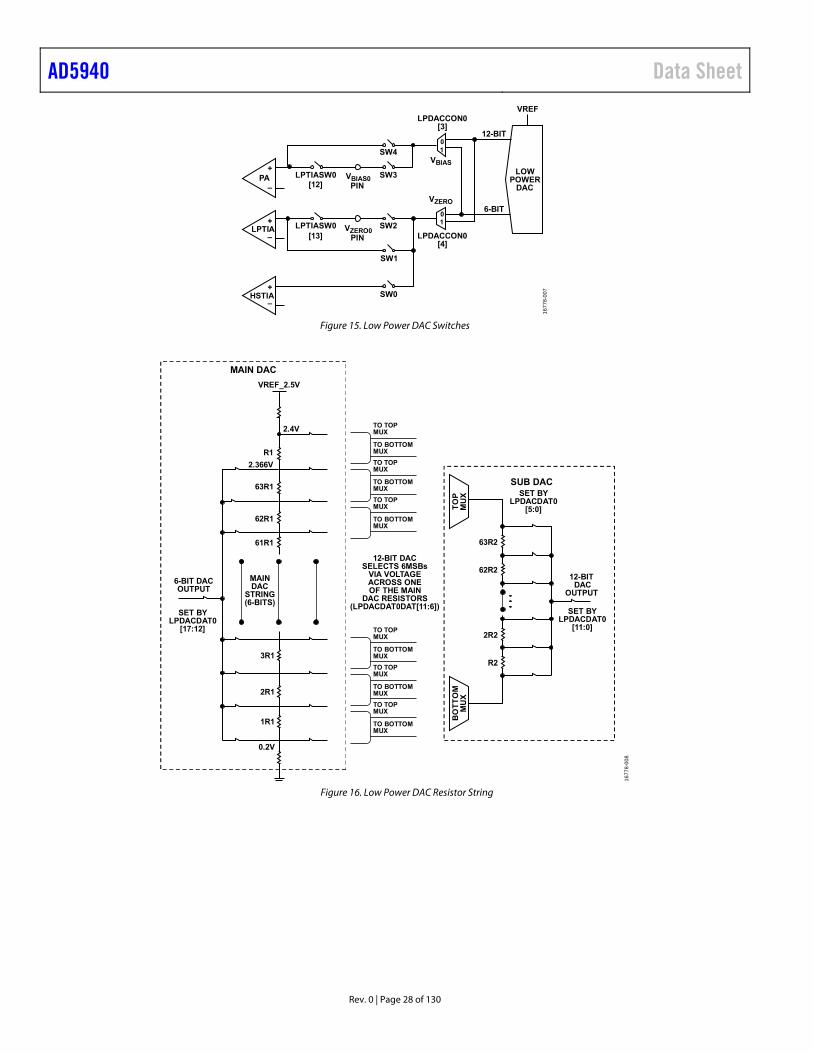
LOW POWER DAC SWITCH OPTIONS There are a number of switch options available that allow the user to configure the low power DAC for various modes of operation. These switches facilitate different use cases, such as electrochemical impedance spectroscopy. Figure 15 shows the available switches, labeled SW0 to SW4. These switches are controlled either automatically via Bit 5 in the LPDACCON0 register, or individually via the LPDACSW0 register
When LPDACCON0, Bit 5, is cleared, the switches are configured for normal mode. The SW2 switch and the SW3 switch are closed and the SW0, SW1, and SW4 switches are open. When LPDACCON0, Bit 5, is set, the switches are configured for diagnostic mode. The SW0 switch and the SW4 switch are closed and the remaining switches are open. This feature is designed for electrochemical use cases, such as continuous glucose measurement where, in normal mode, the low power TIA measures the sense electrode. Then, in diagnostic mode, the high speed TIA measures the sense electrode. By switching the VZERO0 voltage output from the low power TIA to the high speed TIA, the effective bias on the sensor, VBIAS0 − VZERO0, is unaffected. Using the high speed TIA facilitates high bandwidth measurements, such as impedance, ramp, and cyclic voltammetry.
Use the LPDACSW0 register to control the switches individually. LPDACSW0, Bit 5, must be set to 1. Then, each switch can be individually controlled via LPDACSW0, Bits[4:0].
AD5940 Data Sheet
Rev. 0 | Page 28 of 130
LOWPOWER
DAC
0
01
1
VREF
+PA
–
+LPTIA
–
VBIAS0PIN
VZERO0PIN
+HSTIA
–
VBIAS
VZERO
12-BIT
6-BIT
SW0
SW1
SW2
SW3
SW4
LPTIASW0[12]
LPTIASW0[13]
LPDACCON0[3]
LPDACCON0[4]
1677
8-00
7
Figure 15. Low Power DAC Switches
MAIN DAC
VREF_2.5V
2.4V
2.366V
63R1
3R1
2R1
1R1
0.2V
62R1
61R1
R1
2R2
R2
63R2
62R26-BIT DACOUTPUT
12-BIT DAC
OUTPUT
12-BIT DACSELECTS 6MSBs
VIA VOLTAGEACROSS ONEOF THE MAIN
DAC RESISTORS(LPDACDAT0DAT[11:6])
MAINDAC
STRING(6-BITS)
SET BYLPDACDAT0
[17:12]
SET BYLPDACDAT0
[5:0]
SUB DAC
SET BYLPDACDAT0
[11:0]
BO
TT
OM
MU
XT
OP
MU
X
TO TOPMUX
TO BOTTOMMUX
TO TOPMUX
TO BOTTOMMUX
TO TOPMUX
TO BOTTOMMUX
TO TOPMUX
TO BOTTOMMUX
TO TOPMUX
TO BOTTOMMUX
TO TOPMUX
TO BOTTOMMUX
1677
8-00
8
Figure 16. Low Power DAC Resistor String
Data Sheet AD5940
Rev. 0 | Page 29 of 130
RELATIONSHIP BETWEEN THE 12-BIT AND 6-BIT OUTPUTS The 12-bit and 6-bit outputs are mostly independent. However, the selected 12-bit value does have a loading effect on the 6-bit output that must be compensated for in user code, particularly when the 12-bit output level is greater than the 6-bit output.
When the 12-bit output is less than the 6-bit output,
12-Bit DAC Output Voltage = 0.2 V + (LPDACDAT0, Bits[11:0] × 12-BIT_LSB_DAC)
6-Bit DAC Output Voltage = 0.2 V + (LPDACDAT0, Bits[17:12] × 6-BIT_LSB_DAC) – 12-BIT_LSB_DAC)
When the 12-bit output is ≥ the 6-bit output,
12-Bit DAC Output Voltage = 0.2 V + (LPDACDAT0, Bits[11:0] × 12-BIT_LSB_DAC)
6-Bit DAC Output Voltage = 0.2 V + (LPDACDAT0, Bits[17:12] × 6-BIT_LSB_DAC)
Therefore, in user code, it is recommended to add the following:
12BITCODE = LPDACDAT0 [11:0];
6BITCODE = LPDACDAT0 [17:12];
if (12BITCODE < (6BITCODE *64))
LPDACDAT [11:0] = (12BITCODE – 1);
This code ensures that the 12-bit output voltage is equal to the 6-bit output voltage when LPDACDAT0, Bits[11:0] = 64 × LPDACDAT0, Bits[17:12].
LOW POWER DAC USE CASES Electrochemical Amperometric Measurement
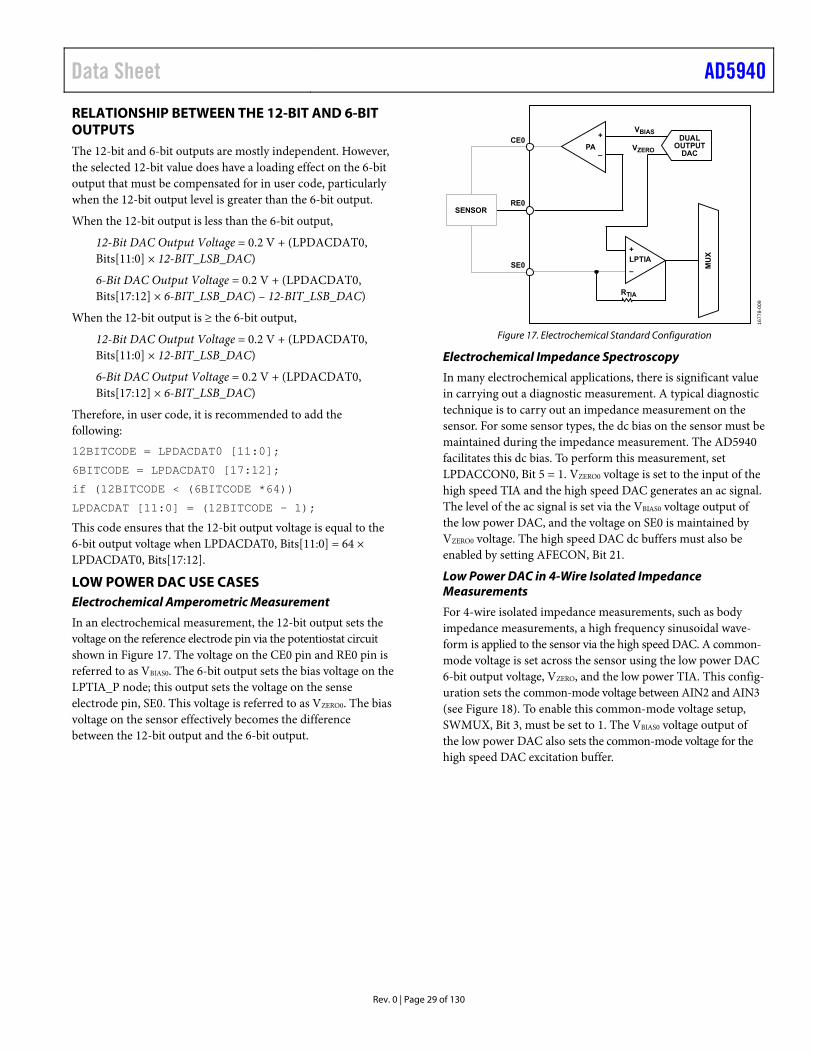
In an electrochemical measurement, the 12-bit output sets the voltage on the reference electrode pin via the potentiostat circuit shown in Figure 17. The voltage on the CE0 pin and RE0 pin is referred to as VBIAS0. The 6-bit output sets the bias voltage on the LPTIA_P node; this output sets the voltage on the sense electrode pin, SE0. This voltage is referred to as VZERO0. The bias voltage on the sensor effectively becomes the difference between the 12-bit output and the 6-bit output.
PADUAL
OUTPUTDAC
MU
X
RE0
RTIA
VBIAS
VZERO
SE0
CE0
SENSOR
+LPTIA
–
+
–
1677
8-00
9
Figure 17. Electrochemical Standard Configuration
Electrochemical Impedance Spectroscopy
In many electrochemical applications, there is significant value in carrying out a diagnostic measurement. A typical diagnostic technique is to carry out an impedance measurement on the sensor. For some sensor types, the dc bias on the sensor must be maintained during the impedance measurement. The AD5940 facilitates this dc bias. To perform this measurement, set LPDACCON0, Bit 5 = 1. VZERO0 voltage is set to the input of the high speed TIA and the high speed DAC generates an ac signal. The level of the ac signal is set via the VBIAS0 voltage output of the low power DAC, and the voltage on SE0 is maintained by VZERO0 voltage. The high speed DAC dc buffers must also be enabled by setting AFECON, Bit 21.
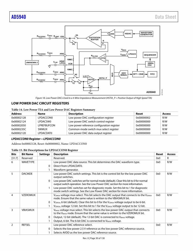
Low Power DAC in 4-Wire Isolated Impedance Measurements
For 4-wire isolated impedance measurements, such as body impedance measurements, a high frequency sinusoidal wave-form is applied to the sensor via the high speed DAC. A common-mode voltage is set across the sensor using the low power DAC 6-bit output voltage, VZERO, and the low power TIA. This config-uration sets the common-mode voltage between AIN2 and AIN3 (see Figure 18). To enable this common-mode voltage setup, SWMUX, Bit 3, must be set to 1. The VBIAS0 voltage output of the low power DAC also sets the common-mode voltage for the high speed DAC excitation buffer.
AD5940 Data Sheet
Rev. 0 | Page 30 of 130
GAIN
EXCITATIONBUFFER
+HSTIA–
ADC/800kHz DFT = 2048 FIFO
16MHzOSC
SEQUENCERAIN2
AIN3
AIN1
CE0
MU
X
RTIA
10MΩ
RLIMIT
T2 T9
N2
D5
P5
VCM
HSTIA_P
AD5940
CISO1
1.1V
UNKNOWN Z
RACCESS1
CISO3
CISO4
CISO2
RACCESS3
RACCESS4
RACCESS2
AIN4/LPF0CLPF
HSDAC WAVEFORMGENERATOR
LPDAC0+
LSTIA–
RFILTER
CTIA
VZERO
VBIAS
PN
10MΩ
1677
8-01
0
Figure 18. Low Power DACs Used in a 4-Wire Impedance Measurement (HSTIA_P = Positive Output of High Speed TIA)
LOW POWER DAC CIRCUIT REGISTERS
Table 14. Low Power TIA and Low Power DAC Registers Summary Address Name Description Reset Access 0x00002128 LPDACCON0 Low power DAC configuration register 0x00000002 R/W 0x00002124 LPDACSW0 Low power DAC switch control register 0x00000000 R/W 0x00002050 LPREFBUFCON Low power reference configuration register 0x00000000 R/W 0x0000235C SWMUX Common-mode switch mux select register 0x00000000 R/W 0x00002120 LPDACDAT0 Low power DAC data output register 0x00000000 R/W
LPDACCON0 Register—LPDACCON0
Address 0x00002128, Reset: 0x00000002, Name: LPDACCON0
Table 15. Bit Descriptions for LPDACCON0 Register Bits Bit Name Settings Description Reset Access [31:7] Reserved Reserved. 0x0 R 6 WAVETYPE Low power DAC data source. This bit determines the DAC waveform type. 0x0 R/W 0 Direct from LPDACDAT0. 1 Waveform generator. 5 DACMDE Low power DAC switch settings. This bit is the control bit for the low power DAC
output switches. 0x0 R/W
0 Low power DAC switches set for normal mode (default). Clear this bit to 0 for normal output switch operation. See the Low Power DAC section for more information.
1 Low power DAC switches set for diagnostic mode. Set this bit to 1 for diagnostic mode switch settings. See the Low Power DAC section for more information.
4 VZEROMUX VZERO0 voltage mux select. This bit selects the DAC output that connects to the VZERO0 node. Ensure that the same value is written to the VBIASMUX bit.
0x0 R/W
0 VZERO0, 6-bit (default). Clear this bit to 0 for the VZERO0 voltage output to be 6-bit. 1 VZERO0, voltage 12-bit. Set this bit to 1 for the VZERO0 voltage output to be 12-bit. 3 VBIASMUX VBIAS0 voltage mux select. This bit selects the low power DAC output that connects
to the VBIAS0 node. Ensure that the same value is written to the VZEROMUX bit. 0x0 R/W
0 Output, 12-bit (default). The 12-bit DAC is connected to VBIAS0 voltage. 1 Output, 6-bit. The 6-bit DAC is connected to VBIAS0 voltage. 2 REFSEL Low power DAC reference select. 0x0 R/W 0 Selects the low power 2.5 V reference as the low power DAC reference source. 1 Selects AVDD as the low power DAC reference source.
Data Sheet AD5940
Rev. 0 | Page 31 of 130
Bits Bit Name Settings Description Reset Access 1 PWDEN Low power DAC power-down. This bit powers down the control bit for the low
power DAC. 0x1 R/W
0 Low Power DAC powered on. Clear this bit to 0 to power on the low power DAC. 1 Low Power DAC powered off (default). Powers down the low power DAC and opens
all switches on the low power DAC output.
0 RSTEN Enable writes to low power DAC. Enables writes to LPDACDAT0 register. 0x0 R/W 0 Disables low power DAC writes (default). If this bit is cleared to 0, LPDACDAT0 is
always 0. Writes to LPDACDAT0 are disabled.
1 Enables low power DAC writes. Set this bit to 1 to enable writes to LPDACDAT0.
Low Power DAC Switch Control Register—LPDACSW0
Address 0x00002124, Reset: 0x00000000, Name: LPDACSW0
Table 16. Bit Descriptions for LPDACSW0 Register Bits Bit Name Settings Description Reset Access [31:6] Reserved Reserved. 0x0 R 5 LPMODEDIS Switch control. This bit controls the switches connected to the output of the low
power DAC. 0x0 R/W
0 Low power DAC switch controlled by LPDACCON0, Bit 5 (default). Clear this bit to 0 to control the switches connected to the output of the low power DAC via LPDACCON0, Bit 5.
1 Low power DAC switches override. Set this bit to 1 to overrides LPDACCON0, Bit 5. The switches connected to the Low Power DAC output are controlled via LPDACSW0, Bits[4:0].
4 SW4 Low power DAC SW4 switch control. 0x0 R/W 0 Disconnects the direct connection of the VBIAS0 DAC output to the positive input of
low power Amplifier 0 (default).
1 Connects the VBIAS0 DAC voltage output directly to the positive input of low power Amplifier 0.
3 SW3 Low power DAC SW3 switch control. 0x1 0 Disconnects the VBIAS0 DAC voltage output from the low-pass filter/VBIAS0 pin. R/W 1 Connects the VBIAS0 DAC voltage output to the low-pass filter/VBIAS0 pin (default). 2 SW2 Low power DAC SW2 switch control. 0 Disconnects the VZERO0 DAC voltage output from the low-pass filter/VZERO0 pin. 0x1 R/W 1 Connects the VZERO0 DAC voltage output to the low-pass filter/VZERO0 pin (default). 1 SW1 Low power DAC SW1 switch control. 0x0 0 Disconnects the direct connection of the VZERO0 DAC voltage output to the low
power TIA positive input (default). R/W
1 Connects the VZERO0 DAC voltage output directly to the low power TIA positive input.
0 SW0 Low power DAC SW0 switch control. 0x0 0 Disconnects the VZERO0 DAC voltage output from the high speed TIA positive input
(default). R/W
1 Connects the VZERO0 DAC voltage output to the high speed TIA positive input.
Low Power DAC Data Output Register—LPDACDAT0
Address 0x00002120, Reset: 0x00000000, Name: LPDACDAT0
Table 17. Bit Descriptions for LPDACDAT0 Register Bits Bit Name Settings Description Reset Access [31:18] Reserved Reserved. 0x0 R [17:12] DACIN6 Low power DAC 6-bit output data register (1 LSB = 34.375 mV). A value between 0
and 0x3F sets the 6-bit output voltage. 0x0 R/W
0 Sets output voltage to 0.2 V. 111111 Sets output voltage to 2.366 V.
AD5940 Data Sheet
Rev. 0 | Page 32 of 130
Bits Bit Name Settings Description Reset Access [11:0] DACIN12 Low power DAC 12-bit output data register (1 LSB = 537 µV). A value between 0 and
0xFFF sets the 12-bit output voltage. 0x0 R/W
0 Sets output voltage to 0.2 V. 0xFFF Sets output voltage to 2.4 V.
Low Power Reference Control Register—LPREFBUFCON
Address 0x00002050, Reset: 0x00000000, Name: LPREFBUFCON
Table 18. Bit Descriptions for LPREFBUFCON Register Bits Bit Name Settings Description Reset Access [31:2] Reserved Reserved. 0x0 R 1 LPBUF2P5DIS Low power output band gap buffer. This bit is normally cleared to enable the
low power reference buffer. 0x0 R/W
0 Enables the low power 2.5 V buffer. 1 Powers down the low power 2.5 V buffer. 0 LPREFDIS Low power band gap power-down bit. This bit is normally cleared to enable the
low power reference. 0x0 R/W
0 Low power reference enabled.
1 Low power reference powered down.
Common-Mode Switch Mux Register—SWMUX
Address 0x0000235C, Reset: 0x00000000, Name: SWMUX
Table 19. Bit Descriptions for SWMUX Register Bits Bit Name Settings Description Reset Access [31:4] Reserved Reserved. 0x0 R 3 CMMUX Common-mode resistor select for AIN2 pin and AIN3 pin. 0x0 R/W 0 Common-mode switch off. 1 Enables the common-mode switches with a 10 MΩ resistor to set up the common-mode
voltage on the AIN2 and AIN3 pins. The voltage is driven by the low power TIA and the AIN4/LPF0 pin.
[2:0] Reserved Reserved. 0x0 R/W

Data Sheet AD5940
Rev. 0 | Page 33 of 130
LOW POWER POTENTIOSTAT The AD5940 has a low power potentiostat that sets and controls the bias voltage of an electrochemical sensor. Typically, the output of the potentiostat is connected to CE0. The noninverting input is connected to VBIAS0 voltage and the inverting input is connected to RE0 as shown in Figure 17. For an electrochemical cell, the potentiostat maintains the bias voltage on the reference electrode (RE0) by sourcing or sinking current through the counter electrode (CE0).
The output of the potentiostat can be connected to various package pins through the switch matrix (see the Programmable Switch Matrix section for details). There are a number of configurable switch options around the potentiostat to provide numerous configuration options (see Figure 19).
The potentiostat can also be used a standard buffer output to output VBIAS0 voltage onto CE0. To achieve this, the inverting input is connected to the output of the potentiostat by closing the SW10 switch, as shown in Figure 19.
AD5940 Data Sheet
Rev. 0 | Page 34 of 130
LOW POWER TIA The AD5940 has a low power TIA channel that amplifies small current inputs to voltages to be measured by the ADC. The load resistor and gain resistor are internal and programmable. Select the RTIA value that maximizes the ADC input range of ±900 mV when PGA gain is 1 or 1.5. Refer to the Specifications section for the maximum voltage for other PGA settings.
To calculate the required gain resistor, use the following equation:
IMAX = . V
TIAR0 9
where: IMAX is the expected full-scale input current. RTIA is the required gain resistor.
There are a number of switches around the low power TIA circuitry. The LPTIASW0 register configures these switches. Figure 19 shows the available switches. When the TIAGAIN bits (Bits[9:5]) in the LPTIACON0 register are set, these switches are closed automatically. When these switches are closed, there is a force/sense circuit with a low-pass filter resistor (RLPF) and a capacitor on the AIN4/LPF0 pin that acts as a resistor-capacitor (RC) delay circuit. The LPTIA0_P_LPF0 connects the output of the low power TIA low-pass filter to the ADC mux. Analog Devices recommends that the LPTIA0_P_LPF0 mux option be selected as the ADC input when using the low power TIA. It is recommended to connect a 100 nF capacitor between the RC0_0 pin and the RC0_1 pin to stabilize the low power TIA.
LOW POWER TIA PROTECTION DIODES Back to back protection diodes are connected in parallel with the RTIA resistor. These diodes are connected or disconnected by closing or opening SW0, controlled by LPTIASW0, Bit 0.These diodes are intended for use when switching RTIA gain settings to amplify small currents to prevent saturation of the TIA. These diodes have a leakage current specification dependent on the voltage across the diodes. If the differential voltage across the diodes is >200 mV, leakage can be >1 nA. If the voltage is >500 mV, leakage can be >1 μA.
Current-Limit Feature of the Low Power TIA and PA
In addition to the protection diode, the low power TIA also has a built in current limiting feature. If the current sourced or sunk from the low power TIA is greater than the overcurrent limit protection specified in Table 1, the amplifiers clamp the current to this limit. If a sensor attempts to source or sink more than the overcurrent limit during startup, the amplifier clamps the output current. Do not use this feature more frequently or for longer than specified in Table 1.
Low Power TIA Force/Sense Feature
The LPTIACON0[9:5] bits select different gain resistor values for the low power TIA, labeled as RTIA in Figure 19. The force and sense connections shown on the feedback path of the low power TIA are used to avoid voltage (I × R) drops on the switches, which select different RTIA settings for the internal RTIA.
USING AN EXTERNAL RTIA To use an external RTIA resistor, take the following steps:
1. Connect an external RTIA resistor across the RC0_0 pin and the RC0_1 pin.
2. Clear LPTIACON0, Bits[9:5] = 0 to disconnect the internal RTIA resistor from the TIA output terminal.
3. Close the SW9 switch by setting LPTIASW0, Bit 9 = 1. When using the internal RTIA reisistor, open the SW9 switch.
4. Connect an external capacitor in parallel with an external RTIA resistor to maintain loop stability. The recommended value of this external capacitor is 100 nF.
RECOMMENDED SWITCH SETTINGS FOR VARIOUS OPERATING MODES Table 20 describes the recommended switch settings in the low power potentiostat loop for various measurement types. For all measurement types, setting the switch to 1 closes the switch and setting the switch to 0 opens the switch. LPTIASW0[13:0] controls SW13 to SW0, as shown in Figure 19.
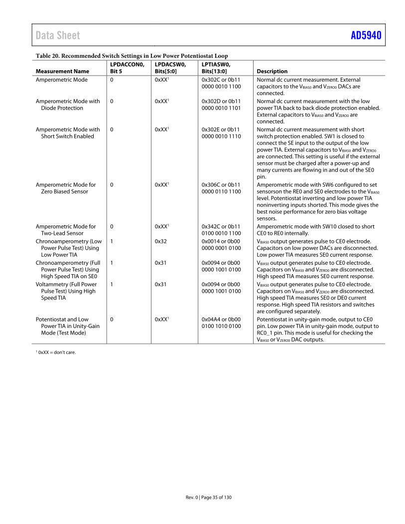
Data Sheet AD5940
Rev. 0 | Page 35 of 130
Table 20. Recommended Switch Settings in Low Power Potentiostat Loop
Measurement Name LPDACCON0, Bit 5
LPDACSW0, Bits[5:0]
LPTIASW0, Bits[13:0] Description
Amperometric Mode 0 0xXX1 0x302C or 0b11 0000 0010 1100
Normal dc current measurement. External capacitors to the VBIAS0 and VZERO0 DACs are connected.
Amperometric Mode with Diode Protection
0 0xXX1 0x302D or 0b11 0000 0010 1101
Normal dc current measurement with the low power TIA back to back diode protection enabled. External capacitors to VBIAS0 and VZERO0 are connected.
Amperometric Mode with Short Switch Enabled
0 0xXX1 0x302E or 0b11 0000 0010 1110
Normal dc current measurement with short switch protection enabled. SW1 is closed to connect the SE input to the output of the low power TIA. External capacitors to VBIAS0 and VZERO0 are connected. This setting is useful if the external sensor must be charged after a power-up and many currents are flowing in and out of the SE0 pin.
Amperometric Mode for Zero Biased Sensor
0 0xXX1 0x306C or 0b11 0000 0110 1100
Amperometric mode with SW6 configured to set sensorson the RE0 and SE0 electrodes to the VBIAS0 level. Potentiostat inverting and low power TIA noninverting inputs shorted. This mode gives the best noise performance for zero bias voltage sensors.
Amperometric Mode for Two-Lead Sensor
0 0xXX1 0x342C or 0b11 0100 0010 1100
Amperometric mode with SW10 closed to short CE0 to RE0 internally.
Chronoamperometry (Low Power Pulse Test) Using Low Power TIA
1 0x32 0x0014 or 0b00 0000 0001 0100
VBIAS0 output generates pulse to CE0 electrode. Capacitors on low power DACs are disconnected. Low power TIA measures SE0 current response.
Chronoamperometry (Full Power Pulse Test) Using High Speed TIA on SE0
1 0x31 0x0094 or 0b00 0000 1001 0100
VBIAS0 output generates pulse to CE0 electrode. Capacitors on VBIAS0 and VZERO0 are disconnected. High speed TIA measures SE0 current response.
Voltammetry (Full Power Pulse Test) Using High Speed TIA
1 0x31 0x0094 or 0b00 0000 1001 0100
VBIAS0 output generates pulse to CE0 electrode. Capacitors on VBIAS0 and VZERO0 are disconnected. High speed TIA measures SE0 or DE0 current response. High speed TIA resistors and switches are configured separately.
Potentiostat and Low Power TIA in Unity-Gain Mode (Test Mode)
0 0xXX1 0x04A4 or 0b00 0100 1010 0100
Potentiostat in unity-gain mode, output to CE0 pin. Low power TIA in unity-gain mode, output to RC0_1 pin. This mode is useful for checking the VBIAS0 or VZERO0 DAC outputs.
1 0xXX = don’t care.
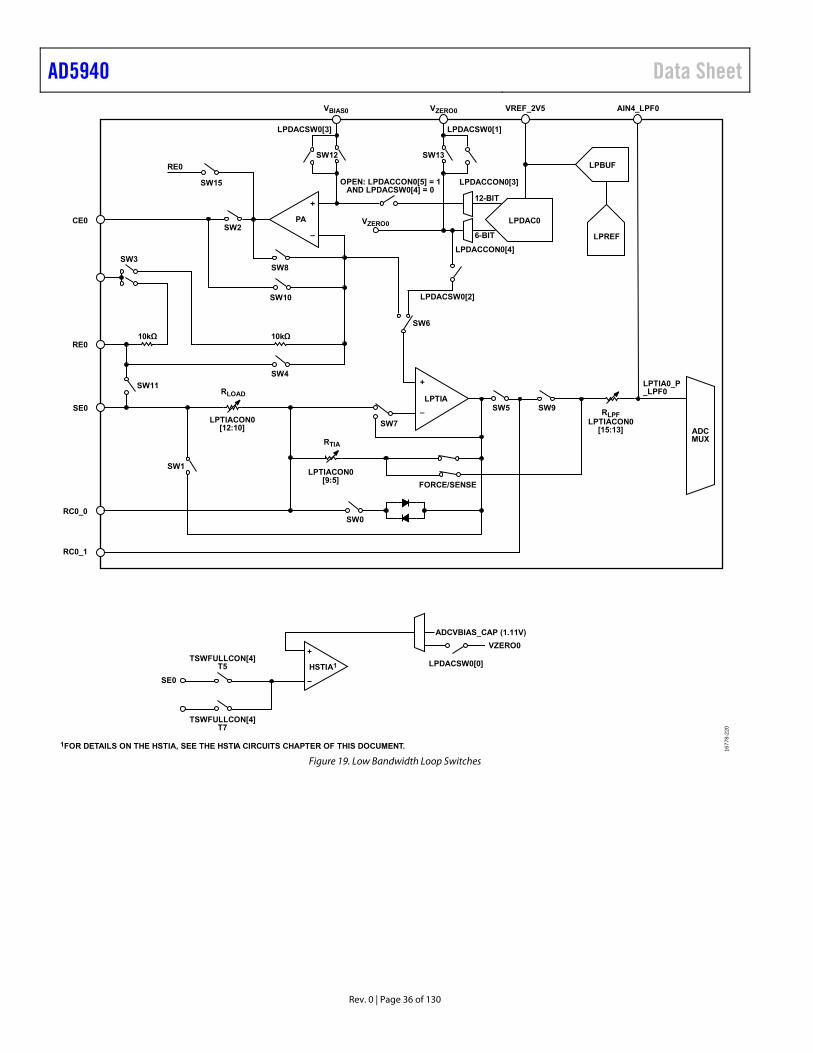
AD5940 Data Sheet
Rev. 0 | Page 36 of 130
+
PA
–SW2
SW13
+
LPTIA
–
SW7
10kΩ
SW3
SW4
SW10
SW8
SW15
RE0
SW6
SW1
SW5
SW0
SW11RLOAD
LPTIACON0[9:5]
LPTIACON0[12:10]
CE0
RE0
SE0
RC0_0
RC0_1
SE0
TSWFULLCON[4]T5
TSWFULLCON[4]T7
VBIAS0
LPDACSW0[3]
OPEN: LPDACCON0[5] = 1AND LPDACSW0[4] = 0
LPDACCON0[3]
LPDACCON0[4]
VZERO0 VREF_2V5 AIN4_LPF0
LPTIA0_P_LPF0
FORCE/SENSE
RLPFLPTIACON0
[15:13]
SW9
10kΩ
RTIA
LPDAC0
12-BIT
6-BIT
LPBUF
LPREF
SW12
LPDACSW0[1]
LPDACSW0[2]
ADCMUX
ADCVBIAS_CAP (1.11V)
VZERO0
LPDACSW0[0]
VZERO0
HSTIA1
1FOR DETAILS ON THE HSTIA, SEE THE HSTIA CIRCUITS CHAPTER OF THIS DOCUMENT. 1677
8-22
0
Figure 19. Low Bandwidth Loop Switches
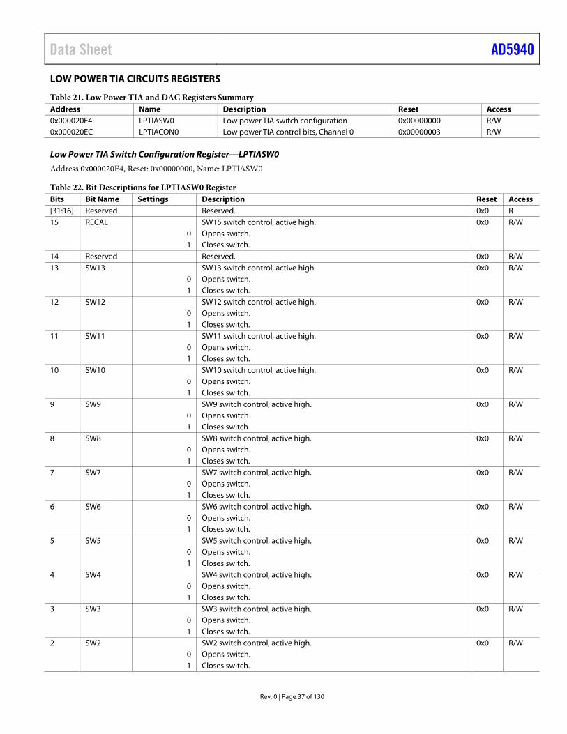
Data Sheet AD5940
Rev. 0 | Page 37 of 130
LOW POWER TIA CIRCUITS REGISTERS
Table 21. Low Power TIA and DAC Registers Summary Address Name Description Reset Access 0x000020E4 LPTIASW0 Low power TIA switch configuration 0x00000000 R/W 0x000020EC LPTIACON0 Low power TIA control bits, Channel 0 0x00000003 R/W
Low Power TIA Switch Configuration Register—LPTIASW0
Address 0x000020E4, Reset: 0x00000000, Name: LPTIASW0
Table 22. Bit Descriptions for LPTIASW0 Register Bits Bit Name Settings Description Reset Access [31:16] Reserved Reserved. 0x0 R 15 RECAL SW15 switch control, active high. 0x0 R/W 0 Opens switch. 1 Closes switch. 14 Reserved Reserved. 0x0 R/W 13 SW13 SW13 switch control, active high. 0x0 R/W 0 Opens switch. 1 Closes switch. 12 SW12 SW12 switch control, active high. 0x0 R/W 0 Opens switch. 1 Closes switch. 11 SW11 SW11 switch control, active high. 0x0 R/W 0 Opens switch. 1 Closes switch. 10 SW10 SW10 switch control, active high. 0x0 R/W 0 Opens switch. 1 Closes switch. 9 SW9 SW9 switch control, active high. 0x0 R/W 0 Opens switch. 1 Closes switch. 8 SW8 SW8 switch control, active high. 0x0 R/W 0 Opens switch. 1 Closes switch. 7 SW7 SW7 switch control, active high. 0x0 R/W 0 Opens switch. 1 Closes switch. 6 SW6 SW6 switch control, active high. 0x0 R/W 0 Opens switch. 1 Closes switch. 5 SW5 SW5 switch control, active high. 0x0 R/W 0 Opens switch. 1 Closes switch. 4 SW4 SW4 switch control, active high. 0x0 R/W 0 Opens switch. 1 Closes switch. 3 SW3 SW3 switch control, active high. 0x0 R/W 0 Opens switch. 1 Closes switch. 2 SW2 SW2 switch control, active high. 0x0 R/W 0 Opens switch. 1 Closes switch.
AD5940 Data Sheet
Rev. 0 | Page 38 of 130
Bits Bit Name Settings Description Reset Access 1 SW1 SW1 switch control, active high. 0x0 R/W 0 Opens switch. 1 Closes switch. 0 SW0 SW0 switch control, active high. 0x0 R/W 0 Opens switch. 1 Closes switch.
Low Power TIA Control Bits, Channel 0 Register—LPTIACON0
Address 0x000020EC, Reset: 0x00000003, Name: LPTIACON0
Table 23. Bit Descriptions for LPTIACON0 Register Bits Bit Name Settings Description Reset Access [31:16] Reserved Reserved. 0x0 R [15:13] TIARF These bits set the low-pass filter resistor (RLPF) and configure the low power TIA output
low-pass filter cutoff frequency. 0x0 R/W
0 Disconnects the TIA output from the low-pass filter pin (LPF0), which is useful for diagnostics where a fast response is required from the ADC. This setting disconnects the low power TIA output from the low-pass filter capacitor.
1 Bypass resistor; 0 Ω option. 10 20 kΩ. 11 100 kΩ. 100 200 kΩ.
101 400 kΩ. 110 600 kΩ. 111 1 MΩ; recommended value for optimal dc current measurement performance. This
setting is the lowest cutoff frequency setting for the low-pass filter.
[12:10] TIARL These bits set RLOAD. 0x0 R/W 0 0 Ω. 1 10 Ω. 10 30 Ω. 11 50 Ω. 100 100 Ω. 101 1.6 kΩ; RTIA must be ≥ 2 kΩ. 110 3.1 kΩ; RTIA must be ≥ 4 kΩ. 111 3.6 kΩ; RTIA must be ≥ 4 kΩ. [9:5] TIAGAIN These bits set the RTIA. 0x0 R/W 0 Disconnects the RTIA. 1 200 Ω. The RTIA is combination of RLOAD and a fixed series 110 Ω. Assumes RLOAD = 10 Ω.
Set by the TIARL bits. RTIA = 100 Ω − RLOAD + 110 Ω. The fixed overall RTIA = 200 Ω.
10 1 kΩ. If RLOAD ≤ 100 Ω, RTIA = (100 Ω − RLOAD) + 1 kΩ. If RLOAD > 100 Ω, RTIA = 1 kΩ − (RLOAD − 100 Ω).
11 2 kΩ. If RLOAD ≤ 100 Ω, RTIA = (100 Ω − RLOAD) + 2 kΩ. If RLOAD > 100 Ω. RTIA = 2 kΩ − (RLOAD − 100 Ω).
100 3 kΩ. If RLOAD ≤ 100 Ω, RTIA = (100 Ω − RLOAD) + 3 kΩ. If RLOAD > 100 Ω. RTIA = 3 kΩ − (RLOAD − 100 Ω).
101 4 kΩ. If RLOAD ≤ 100 Ω, RTIA = (100 Ω − RLOAD) + 4 kΩ. If RLOAD > 100 Ω. RTIA = 4 kΩ − (RLOAD − 100 Ω).
110 6 kΩ. If RLOAD ≤ 100 Ω, RTIA = (100 Ω − RLOAD) + 6 kΩ. If RLOAD > 100 Ω. RTIA = 6 kΩ − (RLOAD − 100 Ω).
111 8 kΩ. If RLOAD ≤ 100 Ω, RTIA = (100 Ω − RLOAD) + 8 kΩ. If RLOAD > 100 Ω. RTIA = 8 kΩ − (RLOAD − 100 Ω).
1000 10 kΩ. If RLOAD ≤ 100 Ω, RTIA = (100 Ω − RLOAD) + 10 kΩ. If RLOAD > 100 Ω. RTIA = 10 kΩ − (RLOAD − 100 Ω).
Data Sheet AD5940
Rev. 0 | Page 39 of 130
Bits Bit Name Settings Description Reset Access 1001 12 kΩ. If RLOAD ≤ 100 Ω, RTIA = (100 Ω − RLOAD) + 12 kΩ. If RLOAD > 100 Ω. RTIA =
12 kΩ − (RLOAD − 100 Ω).
1010 16 kΩ. If RLOAD ≤ 100 Ω, RTIA = (100 Ω − RLOAD) + 16 kΩ. If RLOAD > 100 Ω. RTIA = 16 kΩ − (RLOAD − 100 Ω).
1011 20 kΩ. If RLOAD ≤ 100 Ω, RTIA = (100 Ω − RLOAD) + 20 kΩ. If RLOAD > 100 Ω. RTIA = 20 kΩ − (RLOAD − 100 Ω).
1100 24 kΩ. If RLOAD ≤ 100 Ω, RTIA = (100 Ω − RLOAD) + 24 kΩ. If RLOAD > 100 Ω. RTIA = 24 kΩ − (RLOAD − 100 Ω).
1101 30 kΩ. If RLOAD ≤ 100 Ω, RTIA = (100 Ω − RLOAD) + 30 kΩ. If RLOAD > 100 Ω. RTIA = 30 kΩ − (RLOAD − 100 Ω).
1110 32 kΩ. If RLOAD ≤ 100 Ω, RTIA = (100 Ω − RLOAD) + 32 kΩ. If RLOAD > 100 Ω. RTIA = 32 kΩ − (RLOAD − 100 Ω).
1111 40 kΩ. If RLOAD ≤ 100 Ω, RTIA = (100 Ω − RLOAD) + 40 kΩ. If RLOAD >100 Ω. RTIA = 40 kΩ − (RLOAD − 100 Ω).
10000 48 kΩ. If RLOAD ≤ 100 Ω, RTIA = (100 Ω − RLOAD) + 48 kΩ. If RLOAD > 100 Ω. RTIA = 48 kΩ − (RLOAD − 100 Ω).
10001 64 kΩ. If RLOAD ≤ 100 Ω, RTIA = (100 Ω − RLOAD) + 64 kΩ. If RLOAD > 100 Ω. RTIA = 64 kΩ − (RLOAD − 100 Ω).
10010 85 kΩ. If RLOAD ≤ 100 Ω, RTIA = (100 Ω − RLOAD) + 85 kΩ. If RLOAD > 100 Ω. RTIA = 85 kΩ − (RLOAD − 100 Ω).
10011 96 kΩ. If RLOAD ≤ 100 Ω, RTIA = (100 Ω − RLOAD) + 96 kΩ. If RLOAD > 100 Ω. RTIA = 96 kΩ − (RLOAD − 100 Ω).
10100 100 kΩ. If RLOAD ≤ 100 Ω, RTIA = (100 Ω − RLOAD) + 100 kΩ. If RLOAD > 100 Ω. RTIA = 100 kΩ − (RLOAD − 100 Ω).
10101 120 kΩ. If RLOAD ≤ 100 Ω, RTIA = (100 Ω − RLOAD) + 120 kΩ. If RLOAD > 100 Ω. RTIA = 120 kΩ − (RLOAD − 100 Ω).
10110 128 kΩ. If RLOAD ≤ 100 Ω, RTIA = (100 Ω − RLOAD) + 128 kΩ. If RLOAD > 100 Ω. RTIA = 128 kΩ − (RLOAD − 100 Ω).
10111 160 kΩ. If RLOAD ≤ 100 Ω, RTIA = (100 Ω − RLOAD) + 160 kΩ. If RLOAD > 100 Ω. RTIA = 160 kΩ − (RLOAD − 100 Ω).
11000 196 kΩ. If RLOAD ≤ 100 Ω, RTIA = (100 Ω − RLOAD) + 196 kΩ. If RLOAD > 100 Ω. RTIA = 196 kΩ − (RLOAD − 100 Ω).
11001 256 kΩ. If RLOAD ≤ 100 Ω, RTIA = (100 Ω − RLOAD) + 256 kΩ. If RLOAD > 100 Ω. RTIA = 256 kΩ − (RLOAD − 100 Ω).
11010 512 kΩ. If RLOAD ≤ 100 Ω, RTIA = (100 Ω − RLOAD) + 512 kΩ. If RLOAD > 100 Ω. RTIA = 512 kΩ − (RLOAD − 100 Ω).
[4:3] IBOOST Current boost control. 0x0 R/W 00 Normal mode. 01 Increase amplifier output stage current to quickly charge external capacitor load. This
setting is intended for use with high current sensors.
10 Double TIA and PA overall quiescent current and increase amplifier bandwidth. This setting is useful for diagnostic tests.
11 Double TIA and PA overall quiescent current and increase output stage current. This setting increases amplifier bandwidth and output current capability.
2 HALFPWR Half power mode select. This control bit reduces the active power consumption of the TIA and PA for Sensor Channel 0.
0x0 R/W
0 Normal mode (default). 1 Reduces PA and TIA current by half. 1 PAPDEN PA power-down. Low power Potentiostat power-down control bit. 0x1 R/W 0 Power-up. 1 Power-down. 0 TIAPDEN TIA power-down. Low power TIA power-down control bit. 0x1 R/W 0 Power-up. 1 Power-down.
AD5940 Data Sheet
Rev. 0 | Page 40 of 130
HIGH SPEED DAC CIRCUITS The 12-bit high speed DAC generates an ac excitation signal when measuring the impedance of an external sensor. Control the DAC output signal directly by writing to a data register or by using the automated waveform generator block. The high speed DAC signal is fed to an excitation amplifier designed specifically to couple the ac signal on top of the normal dc bias voltage of a sensor.
HIGH SPEED DAC OUTPUT SIGNAL GENERATION There are two ways of setting the output voltage of the high speed DAC:
• A direct write to the DAC code register, HSDACDAT. This is a 12-bit register where the most significant bit (MSB) is a sign bit. Writing 0x800 results in a 0 V output. Writing 0x200 results in negative full-scale, and writing 0xE00 results in positive full-scale.
• Use the automatic waveform generator. The waveform generator can be programmed to generate fixed frequency, fixed amplitude signals including, sine, trapezoid and square wave signals. If the user selects the sine wave, options exist to adjust the offset and phase of the output signal.
POWER MODES OF THE HIGH SPEED DAC CORE The reference source of the high speed DAC is an internal 1.82 V precision reference voltage (VREF_1V82 pin). There are three basic modes of operation for the high speed DAC that trade off between power consumption vs. output speed: low power mode, high power mode, and hibernate mode. The high speed DAC can also be placed into hibernate mode when inactive.
Low Power Mode
Low power mode is used when the high speed DAC output signal frequency is <80 kHz.
When configuring the high speed DAC for low power mode, take the following steps:
1. Clear the PMBW register (Bit 0 = 0). 2. In this mode, the system clock to the high speed DAC and
the ADC is 16 MHz. 3. Ensure that CLKSEL, Bits[1:0] = 0 to select a 16 MHz,
internal, high frequency oscillator clock source. Ensure the system clock divide ratio is 1 (CLKCON0, Bits[5:0] = 0 or 1.
4. If the internal high speed oscillator is selected as the system clock source, ensure that the 16 MHz option is selected. Set HSOSCCON, Bit 2 = 1.
High Power Mode
High power mode increases the bandwidth supported by the high speed DAC amplifiers. Use high power mode when the high speed DAC frequency is greater than 80 kHz. To enter high power mode, a number of register writes are required.
To configure the high speed DAC for high power mode, take the following steps:
1. Set the PMBW register, Bit 0 = 1. Power consumption is increased, but the output signal bandwidth increases to a maximum of 200 kHz. In high power mode, the system clock to the DAC and the ADC is 32 MHz.
2. Ensure that CLKSEL, Bits[1:0] select a 32 MHz clock source. For example, to select internal high speed oscillator set CLKSEL, Bits[1:0] (SYSCLKSEL) = 00. Ensure that the system clock divide ratio is 1 (CLKCON0, Bits[5:0] = 0 or 1).
3. If the internal high speed oscillator is selected as the system clock source, ensure that the 32 MHz option is selected. Clear HSOSCCON, Bit 2 = 0.
Hibernate Mode
When the AD5940 enters hibernate mode, the clocks to the high speed DAC circuits are clock gated to save power. When in active mode and the high speed DAC is not in use, disable the clocks to save power.
HIGH SPEED DAC FILTER OPTIONS The output stage of the high speed DAC features a configurable reconstruction filter. The configuration of the reconstruction filter is dependent on the output signal frequency of the DAC.
Bits[3:2] in the PMBW register configure the 3 dB cutoff frequency of the reconstruction filter. Ensure that the cutoff frequency is higher than the required DAC output frequency.
• PMBW, Bits[3:2] = 01 for optimal performance if the DAC update frequency is ≤50 kHz.
• PMBW, Bits[3:2] = 10 for optimal performance if the DAC update rate is ≤100 kHz.
• PMBW, Bits[3:2] = 11 for optimal performance if the DAC update rate is up to 250 kHz.
DAC CODE DIRECT
WAVEFORMGENERATOR
RECONSTRUCTIONFILTER
PROGRAMMABLEGAIN
AMPLIFIER
HIGHSPEED
DAC
VBIAS FROMLOW POWER DAC
VZERO FROMLOW POWER DAC
EXCITATIONAMPLIFIER
OUTPUTD+
–
1677
8-22
1
Figure 20. High Speed DAC Block
Data Sheet AD5940
Rev. 0 | Page 41 of 130
HIGH SPEED DAC OUTPUT ATTENUATION OPTIONS Scaling options to modify the output signal amplitude to the sensor are present for the high speed DAC output. The output of the 12-bit DAC string is ±300 mV before any attenuation or gain. At the DAC output, there is a gain stage of 1 or 0.2. At the PGA stage, there are gain options of 2 or 0.25. Table 28 describes the available gain options and the corresponding output voltage ranges.
HIGH SPEED DAC EXCITATION AMPLIFIER Figure 21 illustrates the operation of the excitation amplifier and its connection to the switch matrix. There are four inputs to the excitation amplifier: DACP, DACN, positive (P), and negative (N). The high speed DAC is a differential output DAC where the positive and negative inputs feed directly to the excitation amplifier. The voltage difference between these two outputs sets the peak-to-peak voltage on the output waveform. The P and N inputs maintain the stability of the excitation amplifier by providing a feedback path from the sensor, and set the common-mode for the high speed DAC output. Under normal circumstances, the common mode is set by the VZERO0 output connected to the N input. There is also an option to apply a dc bias voltage to the sensor and couple an ac signal onto this bias, as shown in Figure 22.
An option is available if the sensor requires a bias voltage between the counter and sense electrode. VBIAS0 sets the voltage on the counter electrode (the common-mode voltage of the high speed DAC) and VZERO0 sets the voltage on the sense electrode. VZERO0 must be connected to the positive terminal on the high speed TIA (HSTIACON, Bits[1:0] = 01). The dc buffers of the DAC must also be enabled by setting AFECON, Bit 21. With this configuration, a waveform can be achieved, as shown in Figure 22. The bias across the sensor is effectively the difference between VBIAS0 and VZERO0.
Note that the high speed DAC signal chain must never be used in conjunction with the low power TIA. The high speed DAC can become unstable, leading to incorrect measurements.
+ 2R
+
+–
–
–
R
R PGA12-BITDAC
RCF
DACP
DACN
D
P
N
+
+–
–
VBIAS0
VZERO0
SW
ITC
H M
AT
RIX
DAC DC BUFFERS
2R
AFECON[21]
1677
8-01
4
Figure 21. High Speed DAC Excitation Amplifier
VZERO0
BIAS VOLTAGE
(UP TO 600mV)
VBIAS0
1677
8-01
5
Figure 22. Sensor Excitation Signal
COUPLING AN AC SIGNAL FROM THE HIGH SPEED DAC TO THE DC LEVEL SET BY THE LOW POWER DAC The AD5940 contains a low power potentiostat channel to configure an electrochemical sensor. In normal operation, the bias voltage of the sensor between the RE0 and SE0 electrodes is set by the low power DAC outputs, VBIAS0 and VZERO0, where VBIAS0 sets the bias to the potentiostat and the voltage on the CE0 pin. VZERO0 sets the bias voltage on the low power TIA and the SE0 pin. The high speed DAC circuit is not used. However, for ac impedance measurements, the output of the excitation amplifier must be connected to the CE0 pin. The potentiostat must be disconnected so that the entire signal comes from the excitation amplifier output. The high speed TIA is connected to the SE0 pin and the low power TIA is disconnected. The sensor bias must then be set by the high speed TIA and the excitation amplifier.
To set the sensor bias, take the following steps:
1. The VZERO0 output of the low power DAC must be connected to the noninverting input of the high speed TIA (HSTIACON, Bits[1:0] = 01), which sets the voltage on the SE0 pin, or whichever pin is connected to the inverting input of the high speed TIA via the switch matrix.
2. The DAC dc buffers must be enabled (AFECON, Bit 21 = 1). Figure 21 shows the connection of the dc buffers to the excitation amplifier. These buffers enable the low power DAC outputs to drive the required bias voltage to the excitation amplifier and the high speed TIA.
3. The dc bias is the difference between VBIAS0 and VZERO0.
AVOIDING INCOHERENCY ERRORS BETWEEN EXCITATION AND MEASUREMENT FREQUENCIES DURING IMPEDANCE MEASUREMENTS The following settings are recommended to avoid incoherency errors between excitation and measurement frequencies during impedance measurements:
The Hanning window is always on (DFTCON, Bit 0 = 1). In low power mode, the high speed DAC update rate is
16 MHz or 27 MHz (HSDACCON, Bits[8:1] = 0x1B). In high power mode, the high speed DAC update rate is 32 MHz or 7 MHz (HSDACCON, Bits[8:1] = 0x7).
In low power mode, the ADC sampling rate is 800 kSPS (high frequency oscillator = 16 MHz). In high power mode, the ADC sampling rate is 1.6 MSPS (high frequency oscillator = 32 MHz).
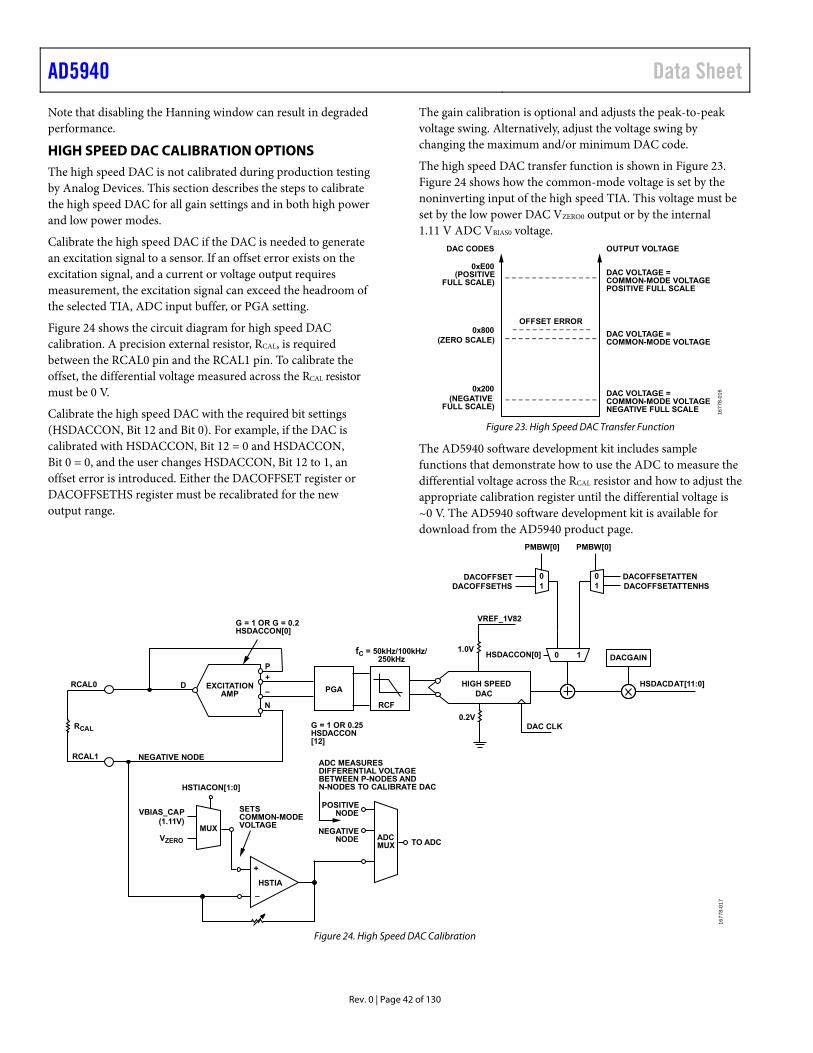
AD5940 Data Sheet
Rev. 0 | Page 42 of 130
Note that disabling the Hanning window can result in degraded performance.
HIGH SPEED DAC CALIBRATION OPTIONS The high speed DAC is not calibrated during production testing by Analog Devices. This section describes the steps to calibrate the high speed DAC for all gain settings and in both high power and low power modes.
Calibrate the high speed DAC if the DAC is needed to generate an excitation signal to a sensor. If an offset error exists on the excitation signal, and a current or voltage output requires measurement, the excitation signal can exceed the headroom of the selected TIA, ADC input buffer, or PGA setting.
Figure 24 shows the circuit diagram for high speed DAC calibration. A precision external resistor, RCAL, is required between the RCAL0 pin and the RCAL1 pin. To calibrate the offset, the differential voltage measured across the RCAL resistor must be 0 V.
Calibrate the high speed DAC with the required bit settings (HSDACCON, Bit 12 and Bit 0). For example, if the DAC is calibrated with HSDACCON, Bit 12 = 0 and HSDACCON, Bit 0 = 0, and the user changes HSDACCON, Bit 12 to 1, an offset error is introduced. Either the DACOFFSET register or DACOFFSETHS register must be recalibrated for the new output range.
The gain calibration is optional and adjusts the peak-to-peak voltage swing. Alternatively, adjust the voltage swing by changing the maximum and/or minimum DAC code.
The high speed DAC transfer function is shown in Figure 23. Figure 24 shows how the common-mode voltage is set by the noninverting input of the high speed TIA. This voltage must be set by the low power DAC VZERO0 output or by the internal 1.11 V ADC VBIAS0 voltage.
DAC CODES OUTPUT VOLTAGE
0xE00(POSITIVE
FULL SCALE)
0x800(ZERO SCALE)
0x200(NEGATIVE
FULL SCALE)
DAC VOLTAGE =COMMON-MODE VOLTAGE
DAC VOLTAGE =COMMON-MODE VOLTAGENEGATIVE FULL SCALE
DAC VOLTAGE =COMMON-MODE VOLTAGEPOSITIVE FULL SCALE
OFFSET ERROR
1677
8-01
6
Figure 23. High Speed DAC Transfer Function
The AD5940 software development kit includes sample functions that demonstrate how to use the ADC to measure the differential voltage across the RCAL resistor and how to adjust the appropriate calibration register until the differential voltage is ~0 V. The AD5940 software development kit is available for download from the AD5940 product page.
VBIAS_CAP(1.11V)
RCAL0
RCAL
+
HSTIA
–
RCAL1
EXCITATIONAMP
D
P
N
+
–HIGH SPEED
DAC
NEGATIVE NODE
ADCMUX
POSITIVENODE
NEGATIVENODE TO ADC
MUX
HSTIACON[1:0]
VREF_1V82
1.0V
0.2V
RCF
fC = 50kHz/100kHz/250kHz
PGA
G = 1 OR 0.25HSDACCON[12]
DAC CLK
HSDACCON[0]
PMBW[0]
DACOFFSET
0 1
01DACOFFSETHS
01
PMBW[0]
DACOFFSETATTENDACOFFSETATTENHS
DACGAIN
HSDACDAT[11:0]
VZERO
SETSCOMMON-MODEVOLTAGE
ADC MEASURESDIFFERENTIAL VOLTAGEBETWEEN P-NODES ANDN-NODES TO CALIBRATE DAC
G = 1 OR G = 0.2HSDACCON[0]
1677
8-01
7
Figure 24. High Speed DAC Calibration
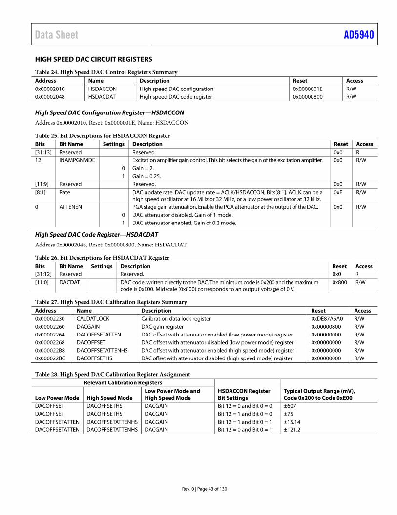
Data Sheet AD5940
Rev. 0 | Page 43 of 130
HIGH SPEED DAC CIRCUIT REGISTERS
Table 24. High Speed DAC Control Registers Summary Address Name Description Reset Access 0x00002010 HSDACCON High speed DAC configuration 0x0000001E R/W 0x00002048 HSDACDAT High speed DAC code register 0x00000800 R/W
High Speed DAC Configuration Register—HSDACCON
Address 0x00002010, Reset: 0x0000001E, Name: HSDACCON
Table 25. Bit Descriptions for HSDACCON Register Bits Bit Name Settings Description Reset Access [31:13] Reserved Reserved. 0x0 R 12 INAMPGNMDE Excitation amplifier gain control. This bit selects the gain of the excitation amplifier. 0x0 R/W 0 Gain = 2. 1 Gain = 0.25. [11:9] Reserved Reserved. 0x0 R/W [8:1] Rate DAC update rate. DAC update rate = ACLK/HSDACCON, Bits[8:1]. ACLK can be a
high speed oscillator at 16 MHz or 32 MHz, or a low power oscillator at 32 kHz. 0xF R/W
0 ATTENEN PGA stage gain attenuation. Enable the PGA attenuator at the output of the DAC. 0x0 R/W 0 DAC attenuator disabled. Gain of 1 mode. 1 DAC attenuator enabled. Gain of 0.2 mode.
High Speed DAC Code Register—HSDACDAT
Address 0x00002048, Reset: 0x00000800, Name: HSDACDAT
Table 26. Bit Descriptions for HSDACDAT Register Bits Bit Name Settings Description Reset Access [31:12] Reserved Reserved. 0x0 R [11:0] DACDAT DAC code, written directly to the DAC. The minimum code is 0x200 and the maximum
code is 0xE00. Midscale (0x800) corresponds to an output voltage of 0 V. 0x800 R/W
Table 27. High Speed DAC Calibration Registers Summary Address Name Description Reset Access 0x00002230 CALDATLOCK Calibration data lock register 0xDE87A5A0 R/W 0x00002260 DACGAIN DAC gain register 0x00000800 R/W 0x00002264 DACOFFSETATTEN DAC offset with attenuator enabled (low power mode) register 0x00000000 R/W 0x00002268 DACOFFSET DAC offset with attenuator disabled (low power mode) register 0x00000000 R/W 0x000022B8 DACOFFSETATTENHS DAC offset with attenuator enabled (high speed mode) register 0x00000000 R/W 0x000022BC DACOFFSETHS DAC offset with attenuator disabled (high speed mode) register 0x00000000 R/W
Table 28. High Speed DAC Calibration Register Assignment Relevant Calibration Registers
HSDACCON Register Bit Settings
Typical Output Range (mV), Code 0x200 to Code 0xE00 Low Power Mode High Speed Mode
Low Power Mode and High Speed Mode
DACOFFSET DACOFFSETHS DACGAIN Bit 12 = 0 and Bit 0 = 0 ±607 DACOFFSET DACOFFSETHS DACGAIN Bit 12 = 1 and Bit 0 = 0 ±75 DACOFFSETATTEN DACOFFSETATTENHS DACGAIN Bit 12 = 1 and Bit 0 = 1 ±15.14 DACOFFSETATTEN DACOFFSETATTENHS DACGAIN Bit 12 = 0 and Bit 0 = 1 ±121.2
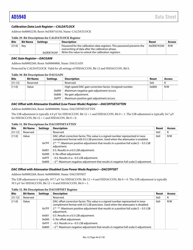
AD5940 Data Sheet
Rev. 0 | Page 44 of 130
Calibration Data Lock Register—CALDATLOCK
Address 0x00002230, Reset: 0xDE87A5A0, Name: CALDATLOCK
Table 29. Bit Descriptions for CALDATLOCK Register Bits Bit Name Settings Description Reset Access [31:0] Key
0xDE87A5AF
Password for the calibration data registers. This password prevents the overwriting of data after the calibration phase. Write this value to unlock the calibration registers.
0xDE87A5A0 R/W
DAC Gain Register—DACGAIN
Address 0x00002260, Reset: 0x00000800, Name: DACGAIN
Protected by CALDATLOCK. Valid for all settings of HSDACCON, Bit 12 and HSDACCON, Bit 0.
Table 30. Bit Descriptions for DACGAIN Bits Bit Name Settings Description Reset Access [31:12] Reserved Reserved. 0x0 R [11:0] Value High speed DAC gain correction factor. Unsigned number. 0x800 R/W 0x000 Maximum negative gain adjustment occurs. 0x800 No gain adjustment. 0xFFF Maximum positive gain adjustment occurs.
DAC Offset with Attenuator Enabled (Low Power Mode) Register—DACOFFSETATTEN
Address 0x00002264, Reset: 0x00000000, Name: DACOFFSETATTEN
The LSB adjustment is typically 4.9 μV for HSDACCON. Bit 12 = 1 and HSDACCON, Bit 0 = 1. The LSB adjustment is typically 24.7 μV for HSDACCON, Bit 12 = 1 and HSDACON, Bit 0 = 0.
Table 31. Bit Descriptions for DACOFFSETATTEN Bits Bit Name Settings Description Reset Access [31:12] Reserved Reserved. 0x0 R [11:0] Value DAC offset correction factor. This value is a signed number represented in twos
complement format with 0.5 LSB precision. Used when the attenuator is enabled. 0x0 R/W
0x7FF 210 − 0.5. Maximum positive adjustment that results in a positive full scale/2 − 0.5 LSB adjustment.
0x001 0.5. Results in a 0.5 LSB adjustment. 0x000 0. No offset adjustment. 0xFFF −0.5. Results in a −0.5 LSB adjustment. 0x800 −210. Maximum negative adjustment that results in negative full scale/2 adjustment.
DAC Offset with Attenuator Disabled (Low Power Mode Register)—DACOFFSET
Address 0x00002268, Reset: 0x00000000, Name: DACOFFSET
The LSB adjustment is typically 197.7 μV for HSDACCON, Bit 12 = 0 and HSDACCON, Bit 0 = 0. The LSB adjustment is typically 39.5 μV for HSDACCON, Bit 12 = 0 and HSDACCON, Bit 0 = 1.
Table 32. Bit Descriptions for DACOFFSET Register Bits Bit Name Settings Description Reset Access [31:12] Reserved Reserved. 0x0 R [11:0] Value DAC offset correction factor. This value is a signed number represented in twos
complement format with 0.5 LSB precision. Used when the attenuator is disabled. 0x0 R/W
0x7FF 210 − 0.5. Maximum positive adjustment that results in a positive full scale/2 − 0.5 LSB adjustment.
0x001 0.5. Results in a 0.5 LSB adjustment. 0x000 0. No offset adjustment. 0xFFF −0.5. Results in a −0.5 LSB adjustment. 0x800 −210. Maximum negative adjustment that results in negative full scale/2 adjustment.
Data Sheet AD5940
Rev. 0 | Page 45 of 130
DAC Offset with Attenuator Enabled (High Speed Mode Register)—DACOFFSETATTENHS
Address 0x000022B8, Reset: 0x00000000, Name: DACOFFSETATTENHS
Protected by CALDATLOCK. The LSB adjustment is typically 4.9 μV for HSDACCON, Bit 12 = 1 and HSDACCON, Bit 0 = 1. The LSB adjustment is typically 24.7 μV for HSDACCON, Bit 12 = 1 and HSDACCON, Bit 0 = 0.
Table 33. Bit Descriptions for DACOFFSETATTENHS Register Bits Bit Name Settings Description Reset Access [31:12] Reserved Reserved. 0x0 R [11:0] Value DAC offset correction factor. This value is a signed number represented in twos
complement format with 0.5 LSB precision. Used when the attenuator is enabled. 0x0 R/W
0x7FF 210 − 0.5. Maximum positive adjustment that results in a positive full scale/2 − 0.5 LSB adjustment.
0x001 0.5. Results in a 0.5 LSB adjustment. 0x000 0. No offset adjustment. 0xFFF −0.5. Results in a −0.5 LSB adjustment. 0x800 −210. Maximum negative adjustment that results in negative full scale/2 adjustment.
DAC Offset with Attenuator Disabled (High Speed Mode Register)—DACOFFSETHS
Address 0x000022BC, Reset: 0x00000000, Name: DACOFFSETHS
Protected by CALDATLOCK. The LSB adjustment is typically 197.7 μV for HSDACCON, Bit 12 = 0 and HSDACCON, Bit 0 = 0. The LSB adjustment is typically 39.5 μV for HSDACCON, Bit 12 = 0 and HSDACCON, Bit 0 = 1.
Table 34. Bit Descriptions for DACOFFSETHS Bits Bit Name Settings Description Reset Access [31:12] Reserved Reserved. 0x0 R [11:0] Value DAC offset correction factor. This value is a signed number represented in twos
complement format with 0.5 LSB precision. Used when the attenuator is disabled. 0x0 R/W
0x7FF 210 − 0.5. Maximum positive adjustment that results in a positive full scale/2 − 0.5 LSB adjustment.
0x001 0.5. Results in a 0.5 LSB adjustment. 0x000 0. No offset adjustment. 0xFFF −0.5. Results in a −0.5 LSB adjustment. 0x800 −210. Maximum negative adjustment that results in negative full scale/2 adjustment.
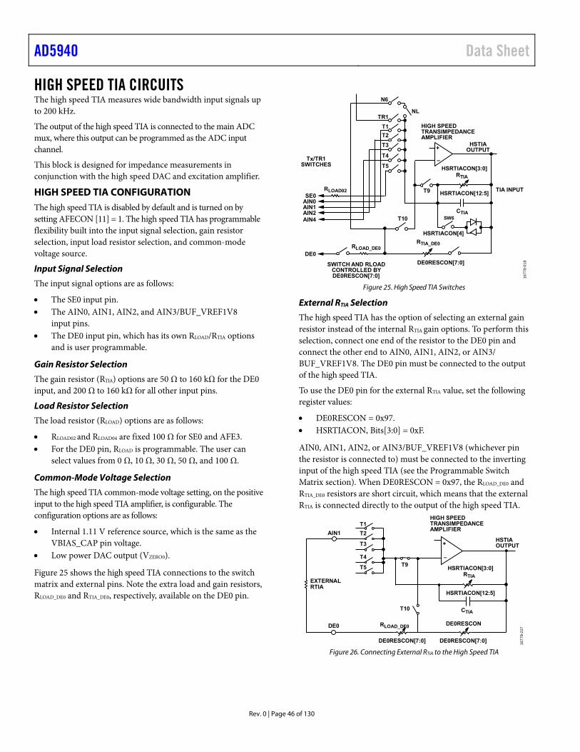
AD5940 Data Sheet
Rev. 0 | Page 46 of 130
HIGH SPEED TIA CIRCUITS The high speed TIA measures wide bandwidth input signals up to 200 kHz.
The output of the high speed TIA is connected to the main ADC mux, where this output can be programmed as the ADC input channel.
This block is designed for impedance measurements in conjunction with the high speed DAC and excitation amplifier.
HIGH SPEED TIA CONFIGURATION The high speed TIA is disabled by default and is turned on by setting AFECON [11] = 1. The high speed TIA has programmable flexibility built into the input signal selection, gain resistor selection, input load resistor selection, and common-mode voltage source.
Input Signal Selection
The input signal options are as follows:
The SE0 input pin. The AIN0, AIN1, AIN2, and AIN3/BUF_VREF1V8
input pins. The DE0 input pin, which has its own RLOAD/RTIA options
and is user programmable.
Gain Resistor Selection
The gain resistor (RTIA) options are 50 Ω to 160 kΩ for the DE0 input, and 200 Ω to 160 kΩ for all other input pins.
Load Resistor Selection
The load resistor (RLOAD) options are as follows:
RLOAD02 and RLOAD04 are fixed 100 Ω for SE0 and AFE3. For the DE0 pin, RLOAD is programmable. The user can
select values from 0 Ω, 10 Ω, 30 Ω, 50 Ω, and 100 Ω.
Common-Mode Voltage Selection
The high speed TIA common-mode voltage setting, on the positive input to the high speed TIA amplifier, is configurable. The configuration options are as follows:
Internal 1.11 V reference source, which is the same as the VBIAS_CAP pin voltage.
Low power DAC output (VZERO0).
Figure 25 shows the high speed TIA connections to the switch matrix and external pins. Note the extra load and gain resistors, RLOAD_DE0 and RTIA_DE0, respectively, available on the DE0 pin.
Tx/TR1SWITCHES
+
–
RTIA
HIGH SPEEDTRANSIMPEDANCEAMPLIFIER
CTIA
TR1NL
T5
T3
T4
T2
T1
TIA INPUT
HSTIAOUTPUT
N6
RTIA_DE0RLOAD_DE0
DE0RESCON[7:0]
HSRTIACON[12:5]
HSRTIACON[3:0]
HSRTIACON[4]
SWITCH AND RLOADCONTROLLED BYDE0RESCON[7:0]
T9
T10
DE0
SE0AIN0AIN1AIN2AIN4
RLOAD02
1677
8-01
8
SW6
Figure 25. High Speed TIA Switches
External RTIA Selection
The high speed TIA has the option of selecting an external gain resistor instead of the internal RTIA gain options. To perform this selection, connect one end of the resistor to the DE0 pin and connect the other end to AIN0, AIN1, AIN2, or AIN3/ BUF_VREF1V8. The DE0 pin must be connected to the output of the high speed TIA.
To use the DE0 pin for the external RTIA value, set the following register values:
DE0RESCON = 0x97. HSRTIACON, Bits[3:0] = 0xF.
AIN0, AIN1, AIN2, or AIN3/BUF_VREF1V8 (whichever pin the resistor is connected to) must be connected to the inverting input of the high speed TIA (see the Programmable Switch Matrix section). When DE0RESCON = 0x97, the RLOAD_DE0 and RTIA_DE0 resistors are short circuit, which means that the external RTIA is connected directly to the output of the high speed TIA.
+
–
HIGH SPEEDTRANSIMPEDANCEAMPLIFIER
T5
T3
T4
T2
T1
HSTIAOUTPUT
DE0RESCON
T9
T10
RTIA
CTIA
HSRTIACON[3:0]
HSRTIACON[12:5]
DE0RESCON[7:0]
RLOAD_DE0
DE0RESCON[7:0]
DE0
AIN1
EXTERNALRTIA
1677
8-22
7
Figure 26. Connecting External RTIA to the High Speed TIA
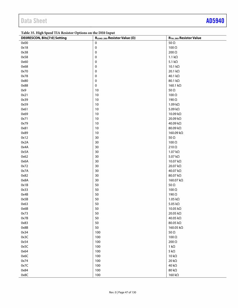
Data Sheet AD5940
Rev. 0 | Page 47 of 130
Table 35. High Speed TIA Resistor Options on the DE0 Input DE0RESCON, Bits[7:0] Setting RLOAD_DE0 Resistor Value (Ω) RTIA_DE0 Resistor Value 0x00 0 50 Ω 0x18 0 100 Ω 0x38 0 200 Ω 0x58 0 1.1 kΩ 0x60 0 5.1 kΩ 0x68 0 10.1 kΩ 0x70 0 20.1 kΩ 0x78 0 40.1 kΩ 0x80 0 80.1 kΩ 0x88 0 160.1 kΩ 0x9 10 50 Ω 0x21 10 100 Ω 0x39 10 190 Ω 0x59 10 1.09 kΩ 0x61 10 5.09 kΩ 0x69 10 10.09 kΩ 0x71 10 20.09 kΩ 0x79 10 40.09 kΩ 0x81 10 80.09 kΩ 0x89 10 160.09 kΩ 0x12 30 50 Ω 0x2A 30 100 Ω 0x4A 30 210 Ω 0x5A 30 1.07 kΩ 0x62 30 5.07 kΩ 0x6A 30 10.07 kΩ 0x72 30 20.07 kΩ 0x7A 30 40.07 kΩ 0x82 30 80.07 kΩ 0x8A 30 160.07 kΩ 0x1B 50 50 Ω 0x33 50 100 Ω 0x4B 50 190 Ω 0x5B 50 1.05 kΩ 0x63 50 5.05 kΩ 0x6B 50 10.05 kΩ 0x73 50 20.05 kΩ 0x7B 50 40.05 kΩ 0x83 50 80.05 kΩ 0x8B 50 160.05 kΩ 0x34 100 50 Ω 0x3C 100 100 Ω 0x54 100 200 Ω 0x5C 100 1 kΩ 0x64 100 5 kΩ 0x6C 100 10 kΩ 0x74 100 20 kΩ 0x7C 100 40 kΩ 0x84 100 80 kΩ 0x8C 100 160 kΩ
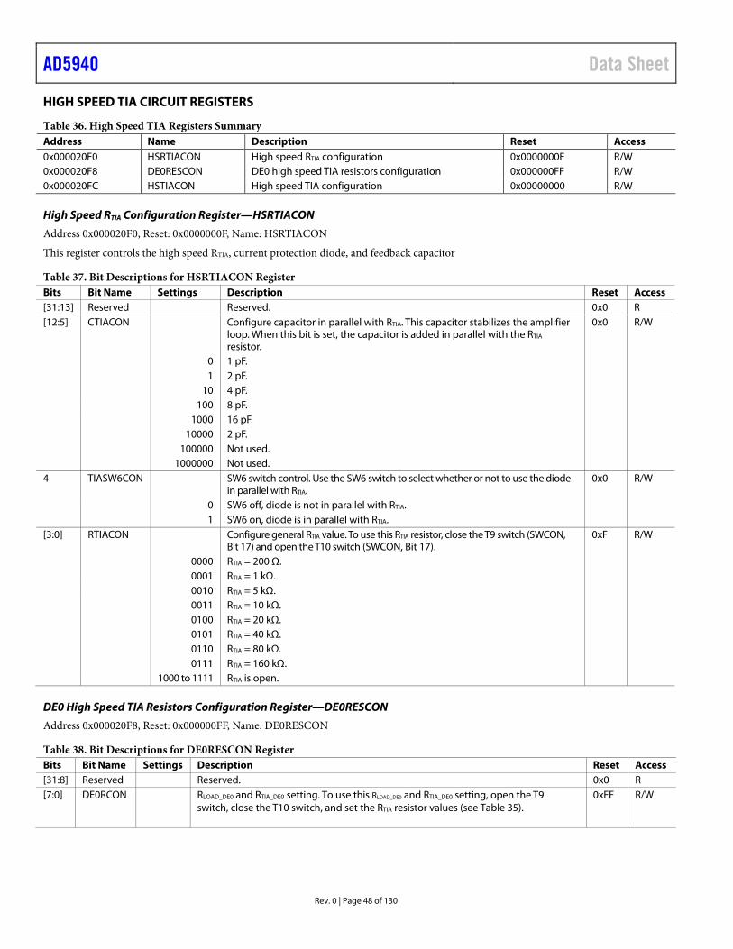
AD5940 Data Sheet
Rev. 0 | Page 48 of 130
HIGH SPEED TIA CIRCUIT REGISTERS
Table 36. High Speed TIA Registers Summary Address Name Description Reset Access 0x000020F0 HSRTIACON High speed RTIA configuration 0x0000000F R/W 0x000020F8 DE0RESCON DE0 high speed TIA resistors configuration 0x000000FF R/W 0x000020FC HSTIACON High speed TIA configuration 0x00000000 R/W
High Speed RTIA Configuration Register—HSRTIACON
Address 0x000020F0, Reset: 0x0000000F, Name: HSRTIACON
This register controls the high speed RTIA, current protection diode, and feedback capacitor
Table 37. Bit Descriptions for HSRTIACON Register Bits Bit Name Settings Description Reset Access [31:13] Reserved Reserved. 0x0 R [12:5] CTIACON Configure capacitor in parallel with RTIA. This capacitor stabilizes the amplifier
loop. When this bit is set, the capacitor is added in parallel with the RTIA resistor.
0x0 R/W
0 1 pF. 1 2 pF.
10 4 pF. 100 8 pF.
1000 16 pF. 10000 2 pF.
100000 Not used. 1000000 Not used.
4 TIASW6CON SW6 switch control. Use the SW6 switch to select whether or not to use the diode in parallel with RTIA.
0x0 R/W
0 SW6 off, diode is not in parallel with RTIA. 1 SW6 on, diode is in parallel with RTIA.
[3:0] RTIACON Configure general RTIA value. To use this RTIA resistor, close the T9 switch (SWCON, Bit 17) and open the T10 switch (SWCON, Bit 17).
0xF R/W
0000 RTIA = 200 Ω. 0001 RTIA = 1 kΩ. 0010 RTIA = 5 kΩ. 0011 RTIA = 10 kΩ. 0100 RTIA = 20 kΩ. 0101 RTIA = 40 kΩ. 0110 RTIA = 80 kΩ. 0111 RTIA = 160 kΩ.
1000 to 1111 RTIA is open.
DE0 High Speed TIA Resistors Configuration Register—DE0RESCON
Address 0x000020F8, Reset: 0x000000FF, Name: DE0RESCON
Table 38. Bit Descriptions for DE0RESCON Register Bits Bit Name Settings Description Reset Access [31:8] Reserved Reserved. 0x0 R [7:0] DE0RCON RLOAD_DE0 and RTIA_DE0 setting. To use this RLOAD_DE0 and RTIA_DE0 setting, open the T9
switch, close the T10 switch, and set the RTIA resistor values (see Table 35). 0xFF R/W
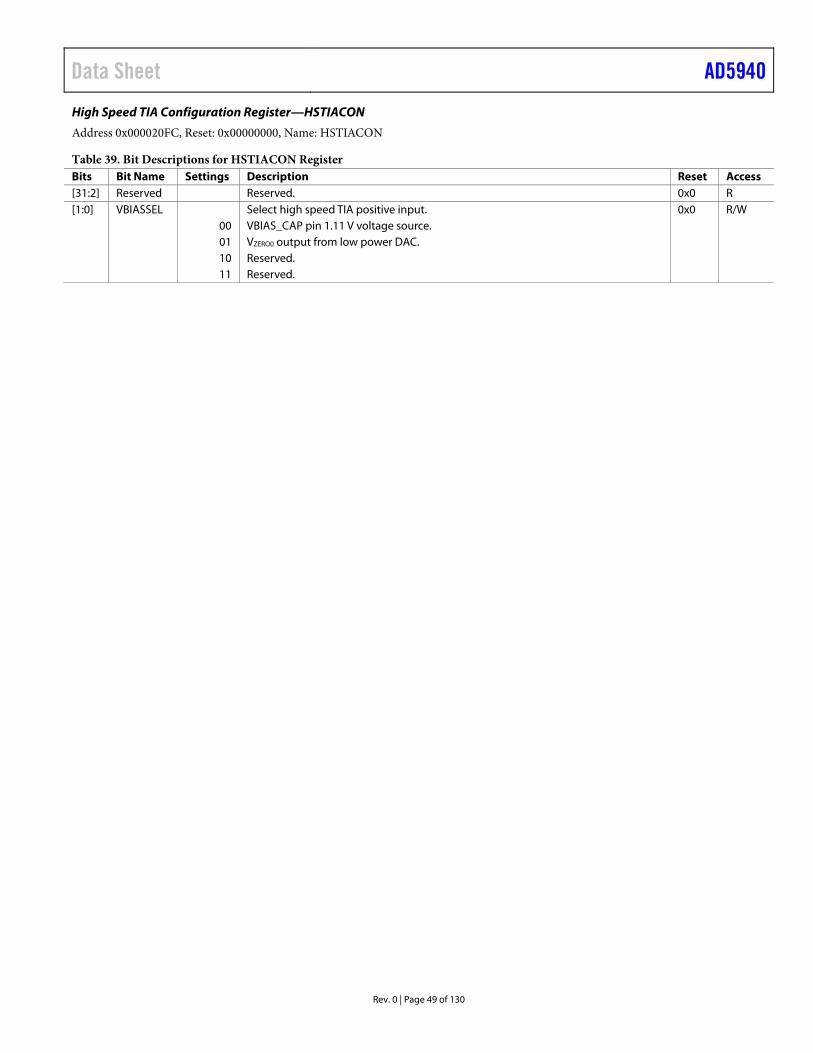
Data Sheet AD5940
Rev. 0 | Page 49 of 130
High Speed TIA Configuration Register—HSTIACON
Address 0x000020FC, Reset: 0x00000000, Name: HSTIACON
Table 39. Bit Descriptions for HSTIACON Register Bits Bit Name Settings Description Reset Access [31:2] Reserved Reserved. 0x0 R [1:0] VBIASSEL Select high speed TIA positive input. 0x0 R/W 00 VBIAS_CAP pin 1.11 V voltage source. 01 VZERO0 output from low power DAC. 10 Reserved. 11 Reserved.
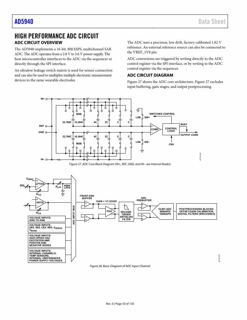
AD5940 Data Sheet
Rev. 0 | Page 50 of 130
HIGH PERFORMANCE ADC CIRCUIT ADC CIRCUIT OVERVIEW The AD5940 implements a 16-bit, 800 kSPS, multichannel SAR ADC. The ADC operates from a 2.8 V to 3.6 V power supply. The host microcontroller interfaces to the ADC via the sequencer or directly through the SPI interface.
An ultralow leakage switch matrix is used for sensor connection and can also be used to multiplex multiple electronic measurement devices to the same wearable electrodes.
The ADC uses a precision, low drift, factory calibrated 1.82 V reference. An external reference source can also be connected to the VREF_1V8 pin.
ADC conversions are triggered by writing directly to the ADC control register via the SPI interface, or by writing to the ADC control register via the sequencer.
ADC CIRCUIT DIAGRAM Figure 27 shows the ADC core architecture. Figure 27 excludes input buffering, gain stages, and output postprocessing.
COMP
SWITCHES CONTROL
BUSY
OUTPUT CODE
CNV
CONTROLLOGIC
SW+LSB
SW–LSB
IN+
REF
GND
IN–
MSB
MSB
CC4C 2C16,384C32,768C
CC4C 2C16,384C32,768C
1677
8-01
9
Figure 27. ADC Core Block Diagram (IN+, REF, GND, and IN− are Internal Nodes)
AD
C I
NP
UT
MU
X
SECOND-ORDER
ANTIALIASFILTER
PGA16-BIT ADC
800kSPS/1600kSPS
GAIN = 1/1.5/2/4/9
–+
+–
–+
+–
FRONT‐ENDBUFFER ADC
PREBUFFER
POSTPROCESSING BLOCKS:OFFSET/GAIN CALIBRATION,
DIGITAL FILTERS (SINC3/SINC2)
+LPTIA0–
RTIA
RLPF
VZERO
SE0
+HSTIA–
RTIA
VOLTAGE INPUTS:AIN0 TO AIN6
VOLTAGE INPUTS:DE0, SE0, CE0, RE0, VZERO0, VBIAS0
VOLTAGE INPUTS:HIGH SPEED DACEXCITATION AMP,POSITIVE ANDNEGATIVE NODES
VOLTAGE INPUTS:INTERNAL CHANNELS:TEMP SENSORS,INTERNAL VREFERENCESPOWER SUPPLY VOLTAGES
AIN4/LPF0
1677
8-22
9
Figure 28. Basic Diagram of ADC Input Channel
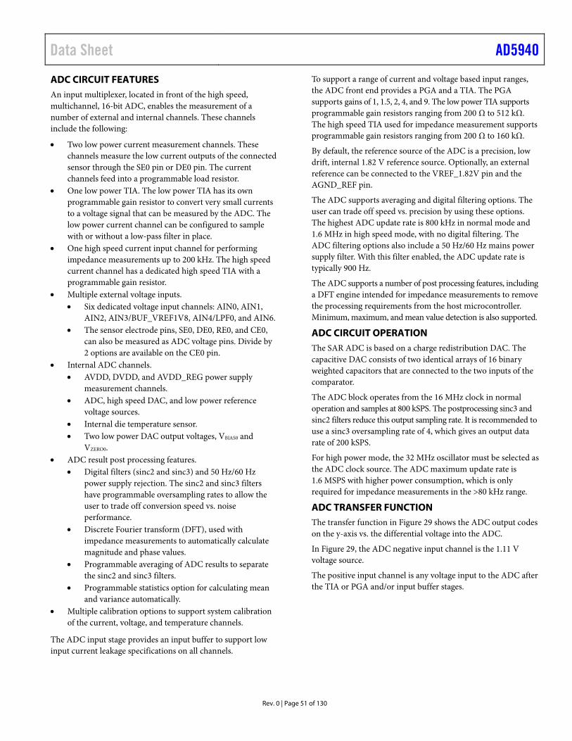
Data Sheet AD5940
Rev. 0 | Page 51 of 130
ADC CIRCUIT FEATURES An input multiplexer, located in front of the high speed, multichannel, 16-bit ADC, enables the measurement of a number of external and internal channels. These channels include the following:
• Two low power current measurement channels. These channels measure the low current outputs of the connected sensor through the SE0 pin or DE0 pin. The current channels feed into a programmable load resistor.
• One low power TIA. The low power TIA has its own programmable gain resistor to convert very small currents to a voltage signal that can be measured by the ADC. The low power current channel can be configured to sample with or without a low-pass filter in place.
• One high speed current input channel for performing impedance measurements up to 200 kHz. The high speed current channel has a dedicated high speed TIA with a programmable gain resistor.
• Multiple external voltage inputs. • Six dedicated voltage input channels: AIN0, AIN1,
AIN2, AIN3/BUF_VREF1V8, AIN4/LPF0, and AIN6. • The sensor electrode pins, SE0, DE0, RE0, and CE0,
can also be measured as ADC voltage pins. Divide by 2 options are available on the CE0 pin.
• Internal ADC channels. • AVDD, DVDD, and AVDD_REG power supply
measurement channels. • ADC, high speed DAC, and low power reference
voltage sources. • Internal die temperature sensor. • Two low power DAC output voltages, VBIAS0 and
VZERO0. • ADC result post processing features.
• Digital filters (sinc2 and sinc3) and 50 Hz/60 Hz power supply rejection. The sinc2 and sinc3 filters have programmable oversampling rates to allow the user to trade off conversion speed vs. noise performance.
• Discrete Fourier transform (DFT), used with impedance measurements to automatically calculate magnitude and phase values.
• Programmable averaging of ADC results to separate the sinc2 and sinc3 filters.
• Programmable statistics option for calculating mean and variance automatically.
• Multiple calibration options to support system calibration of the current, voltage, and temperature channels.
The ADC input stage provides an input buffer to support low input current leakage specifications on all channels.
To support a range of current and voltage based input ranges, the ADC front end provides a PGA and a TIA. The PGA supports gains of 1, 1.5, 2, 4, and 9. The low power TIA supports programmable gain resistors ranging from 200 Ω to 512 kΩ. The high speed TIA used for impedance measurement supports programmable gain resistors ranging from 200 Ω to 160 kΩ.
By default, the reference source of the ADC is a precision, low drift, internal 1.82 V reference source. Optionally, an external reference can be connected to the VREF_1.82V pin and the AGND_REF pin.
The ADC supports averaging and digital filtering options. The user can trade off speed vs. precision by using these options. The highest ADC update rate is 800 kHz in normal mode and 1.6 MHz in high speed mode, with no digital filtering. The ADC filtering options also include a 50 Hz/60 Hz mains power supply filter. With this filter enabled, the ADC update rate is typically 900 Hz.
The ADC supports a number of post processing features, including a DFT engine intended for impedance measurements to remove the processing requirements from the host microcontroller. Minimum, maximum, and mean value detection is also supported.
ADC CIRCUIT OPERATION The SAR ADC is based on a charge redistribution DAC. The capacitive DAC consists of two identical arrays of 16 binary weighted capacitors that are connected to the two inputs of the comparator.
The ADC block operates from the 16 MHz clock in normal operation and samples at 800 kSPS. The postprocessing sinc3 and sinc2 filters reduce this output sampling rate. It is recommended to use a sinc3 oversampling rate of 4, which gives an output data rate of 200 kSPS.
For high power mode, the 32 MHz oscillator must be selected as the ADC clock source. The ADC maximum update rate is 1.6 MSPS with higher power consumption, which is only required for impedance measurements in the >80 kHz range.
ADC TRANSFER FUNCTION The transfer function in Figure 29 shows the ADC output codes on the y-axis vs. the differential voltage into the ADC.
In Figure 29, the ADC negative input channel is the 1.11 V voltage source.
The positive input channel is any voltage input to the ADC after the TIA or PGA and/or input buffer stages.
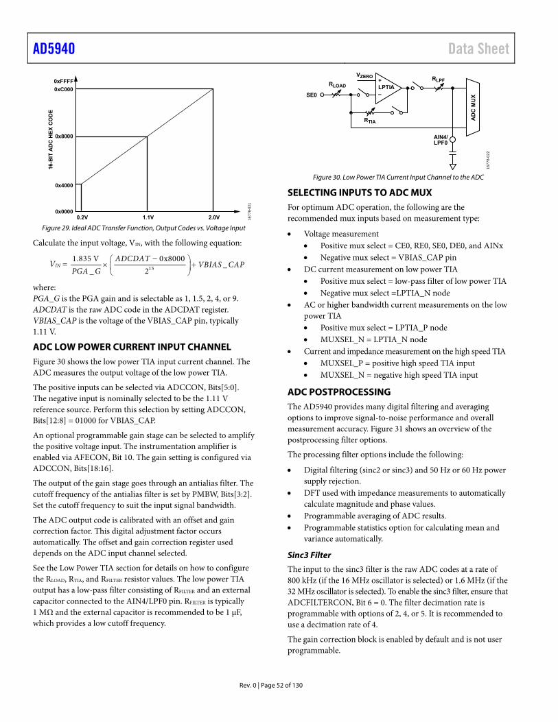
AD5940 Data Sheet
Rev. 0 | Page 52 of 130
0.2V0x0000
0x4000
0x8000
0xC000
0xFFFF
16-B
ITA
DC
HE
X C
OD
E
1.1V 2.0V 1677
8-02
1
Figure 29. Ideal ADC Transfer Function, Output Codes vs. Voltage Input
Calculate the input voltage, VIN, with the following equation:
VIN =
15
1.835 V 0x8000_
_ 2ADCDAT
VBIAS CAPPGA G
where: PGA_G is the PGA gain and is selectable as 1, 1.5, 2, 4, or 9. ADCDAT is the raw ADC code in the ADCDAT register. VBIAS_CAP is the voltage of the VBIAS_CAP pin, typically 1.11 V.
ADC LOW POWER CURRENT INPUT CHANNEL Figure 30 shows the low power TIA input current channel. The ADC measures the output voltage of the low power TIA.
The positive inputs can be selected via ADCCON, Bits[5:0]. The negative input is nominally selected to be the 1.11 V reference source. Perform this selection by setting ADCCON, Bits[12:8] = 01000 for VBIAS_CAP.
An optional programmable gain stage can be selected to amplify the positive voltage input. The instrumentation amplifier is enabled via AFECON, Bit 10. The gain setting is configured via ADCCON, Bits[18:16].
The output of the gain stage goes through an antialias filter. The cutoff frequency of the antialias filter is set by PMBW, Bits[3:2]. Set the cutoff frequency to suit the input signal bandwidth.
The ADC output code is calibrated with an offset and gain correction factor. This digital adjustment factor occurs automatically. The offset and gain correction register used depends on the ADC input channel selected.
See the Low Power TIA section for details on how to configure the RLOAD, RTIA, and RFILTER resistor values. The low power TIA output has a low-pass filter consisting of RFILTER and an external capacitor connected to the AIN4/LPF0 pin. RFILTER is typically 1 MΩ and the external capacitor is recommended to be 1 μF, which provides a low cutoff frequency.
+LPTIA–
RTIA
RLOAD
RLPF
AD
C M
UXSE0
AIN4/LPF0
VZERO
1677
8-02
2
Figure 30. Low Power TIA Current Input Channel to the ADC
SELECTING INPUTS TO ADC MUX For optimum ADC operation, the following are the recommended mux inputs based on measurement type:
Voltage measurement Positive mux select = CE0, RE0, SE0, DE0, and AINx Negative mux select = VBIAS_CAP pin
DC current measurement on low power TIA Positive mux select = low-pass filter of low power TIA Negative mux select =LPTIA_N node
AC or higher bandwidth current measurements on the low power TIA Positive mux select = LPTIA_P node MUXSEL_N = LPTIA_N node
Current and impedance measurement on the high speed TIA MUXSEL_P = positive high speed TIA input MUXSEL_N = negative high speed TIA input
ADC POSTPROCESSING The AD5940 provides many digital filtering and averaging options to improve signal-to-noise performance and overall measurement accuracy. Figure 31 shows an overview of the postprocessing filter options.
The processing filter options include the following:
Digital filtering (sinc2 or sinc3) and 50 Hz or 60 Hz power supply rejection.
DFT used with impedance measurements to automatically calculate magnitude and phase values.
Programmable averaging of ADC results. Programmable statistics option for calculating mean and
variance automatically.
Sinc3 Filter
The input to the sinc3 filter is the raw ADC codes at a rate of 800 kHz (if the 16 MHz oscillator is selected) or 1.6 MHz (if the 32 MHz oscillator is selected). To enable the sinc3 filter, ensure that ADCFILTERCON, Bit 6 = 0. The filter decimation rate is programmable with options of 2, 4, or 5. It is recommended to use a decimation rate of 4.
The gain correction block is enabled by default and is not user programmable.
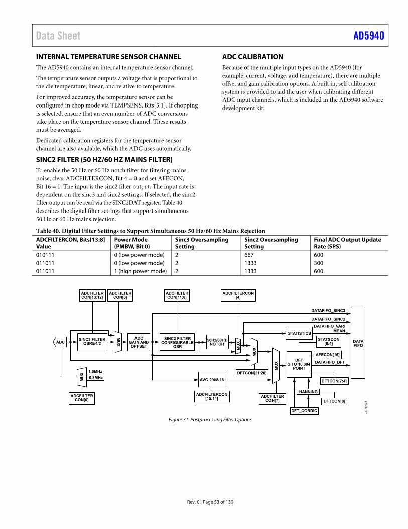
Data Sheet AD5940
Rev. 0 | Page 53 of 130
INTERNAL TEMPERATURE SENSOR CHANNEL The AD5940 contains an internal temperature sensor channel.
The temperature sensor outputs a voltage that is proportional to the die temperature, linear, and relative to temperature.
For improved accuracy, the temperature sensor can be configured in chop mode via TEMPSENS, Bits[3:1]. If chopping is selected, ensure that an even number of ADC conversions take place on the temperature sensor channel. These results must be averaged.
Dedicated calibration registers for the temperature sensor channel are also available, which the ADC uses automatically.
SINC2 FILTER (50 HZ/60 HZ MAINS FILTER) To enable the 50 Hz or 60 Hz notch filter for filtering mains noise, clear ADCFILTERCON, Bit 4 = 0 and set AFECON, Bit 16 = 1. The input is the sinc2 filter output. The input rate is dependent on the sinc3 and sinc2 settings. If selected, the sinc2 filter output can be read via the SINC2DAT register. Table 40 describes the digital filter settings that support simultaneous 50 Hz or 60 Hz mains rejection.
ADC CALIBRATION Because of the multiple input types on the AD5940 (for example, current, voltage, and temperature), there are multiple offset and gain calibration options. A built in, self calibration system is provided to aid the user when calibrating different ADC input channels, which is included in the AD5940 software development kit.
Table 40. Digital Filter Settings to Support Simultaneous 50 Hz/60 Hz Mains Rejection ADCFILTERCON, Bits[13:8] Value
Power Mode (PMBW, Bit 0)
Sinc3 Oversampling Setting
Sinc2 Oversampling Setting
Final ADC Output Update Rate (SPS)
010111 0 (low power mode) 2 667 600 011011 0 (low power mode) 2 1333 300 011011 1 (high power mode) 2 1333 600
DATAFIFO
SINC3 FILTEROSR5/4/2
ADCGAIN ANDOFFSET
SINC2 FILTERCONFIGURABLE
OSR
50Hz/60HzNOTCH
DFT2 TO 16,384
POINT
DFT_CORDIC
HANNING
ADC
MU
X
MU
X
MU
X
STATISTICS
ADCFILTERCON[13:12]
ADCFILTERCON[11:8]
ADCFILTERCON[6]
ADCFILTERCON[4]
MU
X
1.6MHz
0.8MHz
ADCFILTERCON[0]
MU
X
AVG 2/4/8/16
ADCFILTERCON[7] DFTCON[0]
DFTCON[21:20]
DFTCON[7:4]
ADCFILTERCON[15:14]
STATSCON[6:4]
AFECON[15]
DATAFIFO_SINC3
DATAFIFO_SINC2
DATAFIFO_VAR/MEAN
DATAFIFO_DFT16
778-
023
Figure 31. Postprocessing Filter Options
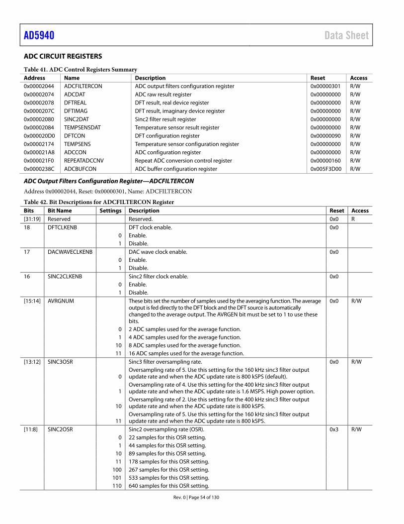
AD5940 Data Sheet
Rev. 0 | Page 54 of 130
ADC CIRCUIT REGISTERS
Table 41. ADC Control Registers Summary Address Name Description Reset Access 0x00002044 ADCFILTERCON ADC output filters configuration register 0x00000301 R/W 0x00002074 ADCDAT ADC raw result register 0x00000000 R/W 0x00002078 DFTREAL DFT result, real device register 0x00000000 R/W 0x0000207C DFTIMAG DFT result, imaginary device register 0x00000000 R/W 0x00002080 SINC2DAT Sinc2 filter result register 0x00000000 R/W 0x00002084 TEMPSENSDAT Temperature sensor result register 0x00000000 R/W 0x000020D0 DFTCON DFT configuration register 0x00000090 R/W 0x00002174 TEMPSENS Temperature sensor configuration register 0x00000000 R/W 0x000021A8 ADCCON ADC configuration register 0x00000000 R/W 0x000021F0 REPEATADCCNV Repeat ADC conversion control register 0x00000160 R/W 0x0000238C ADCBUFCON ADC buffer configuration register 0x005F3D00 R/W
ADC Output Filters Configuration Register—ADCFILTERCON
Address 0x00002044, Reset: 0x00000301, Name: ADCFILTERCON
Table 42. Bit Descriptions for ADCFILTERCON Register Bits Bit Name Settings Description Reset Access [31:19] Reserved Reserved. 0x0 R 18 DFTCLKENB DFT clock enable. 0x0 0 Enable. 1 Disable. 17 DACWAVECLKENB DAC wave clock enable. 0x0 0 Enable. 1 Disable. 16 SINC2CLKENB Sinc2 filter clock enable. 0x0 0 Enable. 1 Disable. [15:14] AVRGNUM
These bits set the number of samples used by the averaging function. The average output is fed directly to the DFT block and the DFT source is automatically changed to the average output. The AVRGEN bit must be set to 1 to use these bits.
0x0 R/W
0 2 ADC samples used for the average function. 1 4 ADC samples used for the average function. 10 8 ADC samples used for the average function. 11 16 ADC samples used for the average function. [13:12] SINC3OSR Sinc3 filter oversampling rate. 0x0 R/W
0 Oversampling rate of 5. Use this setting for the 160 kHz sinc3 filter output update rate and when the ADC update rate is 800 kSPS (default).
1
Oversampling rate of 4. Use this setting for the 400 kHz sinc3 filter output update rate and when the ADC update rate is 1.6 MSPS. High power option.
10
Oversampling rate of 2. Use this setting for the 400 kHz sinc3 filter output update rate and when the ADC update rate is 800 kSPS.
11
Oversampling rate of 5. Use this setting for the 160 kHz sinc3 filter output update rate and when the ADC update rate is 800 kSPS.
[11:8] SINC2OSR Sinc2 oversampling rate (OSR). 0x3 R/W 0 22 samples for this OSR setting. 1 44 samples for this OSR setting. 10 89 samples for this OSR setting. 11 178 samples for this OSR setting. 100 267 samples for this OSR setting. 101 533 samples for this OSR setting. 110 640 samples for this OSR setting.
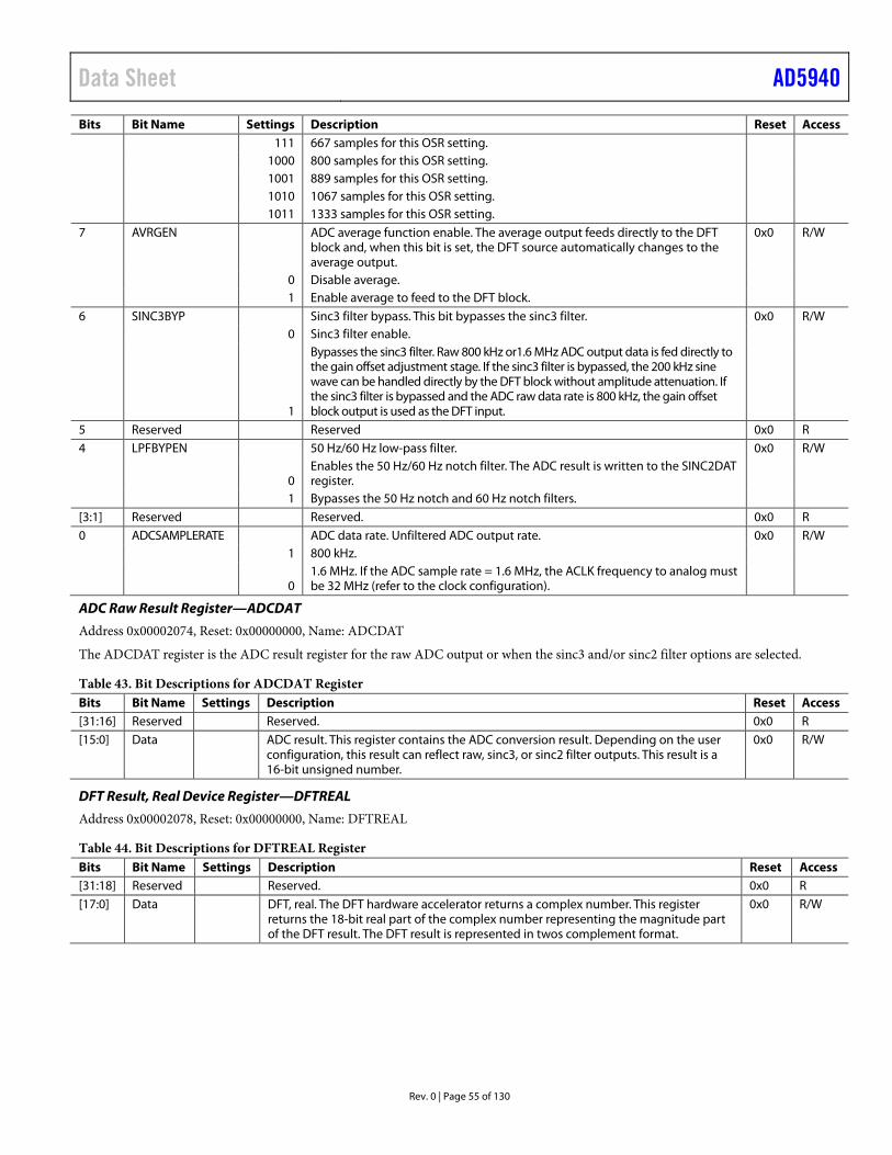
Data Sheet AD5940
Rev. 0 | Page 55 of 130
Bits Bit Name Settings Description Reset Access 111 667 samples for this OSR setting. 1000 800 samples for this OSR setting. 1001 889 samples for this OSR setting. 1010 1067 samples for this OSR setting. 1011 1333 samples for this OSR setting. 7 AVRGEN
ADC average function enable. The average output feeds directly to the DFT block and, when this bit is set, the DFT source automatically changes to the average output.
0x0 R/W
0 Disable average. 1 Enable average to feed to the DFT block. 6 SINC3BYP Sinc3 filter bypass. This bit bypasses the sinc3 filter. 0x0 R/W 0 Sinc3 filter enable.
1
Bypasses the sinc3 filter. Raw 800 kHz or1.6 MHz ADC output data is fed directly to the gain offset adjustment stage. If the sinc3 filter is bypassed, the 200 kHz sine wave can be handled directly by the DFT block without amplitude attenuation. If the sinc3 filter is bypassed and the ADC raw data rate is 800 kHz, the gain offset block output is used as the DFT input.
5 Reserved Reserved 0x0 R 4 LPFBYPEN 50 Hz/60 Hz low-pass filter. 0x0 R/W
0 Enables the 50 Hz/60 Hz notch filter. The ADC result is written to the SINC2DAT register.
1 Bypasses the 50 Hz notch and 60 Hz notch filters. [3:1] Reserved Reserved. 0x0 R 0 ADCSAMPLERATE ADC data rate. Unfiltered ADC output rate. 0x0 R/W 1 800 kHz.
0 1.6 MHz. If the ADC sample rate = 1.6 MHz, the ACLK frequency to analog must be 32 MHz (refer to the clock configuration).
ADC Raw Result Register—ADCDAT
Address 0x00002074, Reset: 0x00000000, Name: ADCDAT
The ADCDAT register is the ADC result register for the raw ADC output or when the sinc3 and/or sinc2 filter options are selected.
Table 43. Bit Descriptions for ADCDAT Register Bits Bit Name Settings Description Reset Access [31:16] Reserved Reserved. 0x0 R [15:0] Data ADC result. This register contains the ADC conversion result. Depending on the user
configuration, this result can reflect raw, sinc3, or sinc2 filter outputs. This result is a 16-bit unsigned number.
0x0 R/W
DFT Result, Real Device Register—DFTREAL
Address 0x00002078, Reset: 0x00000000, Name: DFTREAL
Table 44. Bit Descriptions for DFTREAL Register Bits Bit Name Settings Description Reset Access [31:18] Reserved Reserved. 0x0 R [17:0] Data DFT, real. The DFT hardware accelerator returns a complex number. This register
returns the 18-bit real part of the complex number representing the magnitude part of the DFT result. The DFT result is represented in twos complement format.
0x0 R/W
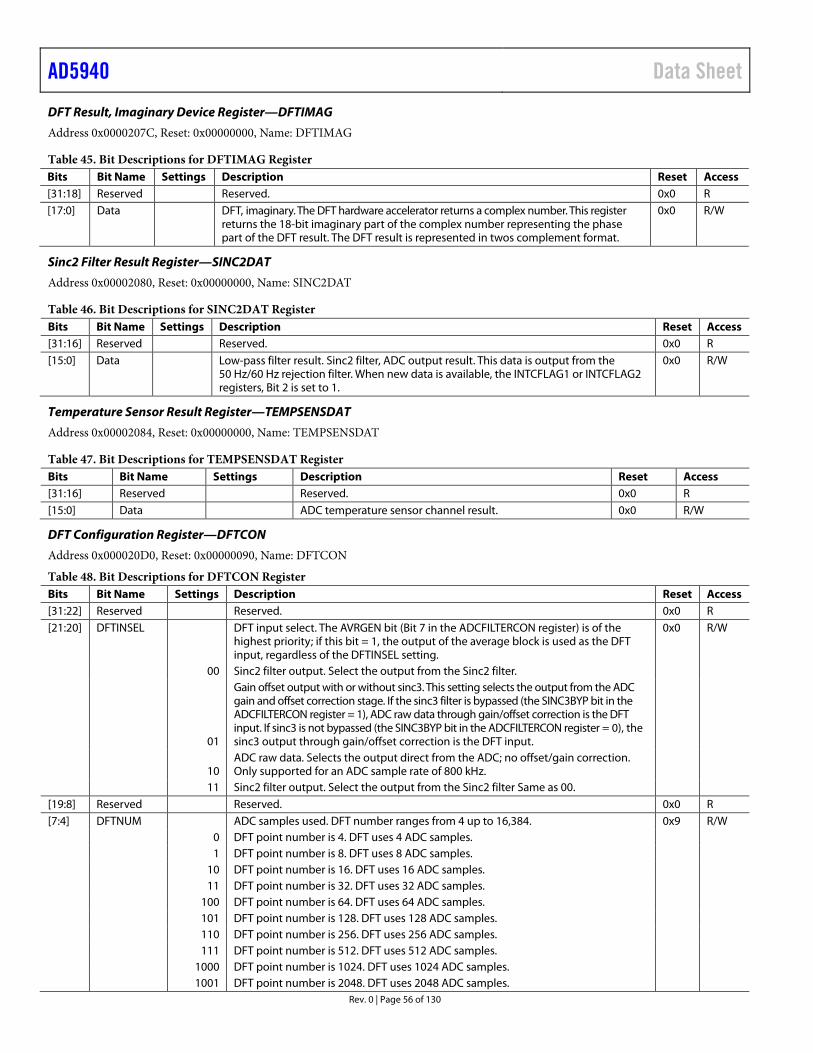
AD5940 Data Sheet
Rev. 0 | Page 56 of 130
DFT Result, Imaginary Device Register—DFTIMAG
Address 0x0000207C, Reset: 0x00000000, Name: DFTIMAG
Table 45. Bit Descriptions for DFTIMAG Register Bits Bit Name Settings Description Reset Access [31:18] Reserved Reserved. 0x0 R [17:0] Data DFT, imaginary. The DFT hardware accelerator returns a complex number. This register
returns the 18-bit imaginary part of the complex number representing the phase part of the DFT result. The DFT result is represented in twos complement format.
0x0 R/W
Sinc2 Filter Result Register—SINC2DAT
Address 0x00002080, Reset: 0x00000000, Name: SINC2DAT
Table 46. Bit Descriptions for SINC2DAT Register Bits Bit Name Settings Description Reset Access [31:16] Reserved Reserved. 0x0 R [15:0] Data Low-pass filter result. Sinc2 filter, ADC output result. This data is output from the
50 Hz/60 Hz rejection filter. When new data is available, the INTCFLAG1 or INTCFLAG2 registers, Bit 2 is set to 1.
0x0 R/W
Temperature Sensor Result Register—TEMPSENSDAT
Address 0x00002084, Reset: 0x00000000, Name: TEMPSENSDAT
Table 47. Bit Descriptions for TEMPSENSDAT Register Bits Bit Name Settings Description Reset Access [31:16] Reserved Reserved. 0x0 R [15:0] Data ADC temperature sensor channel result. 0x0 R/W
DFT Configuration Register—DFTCON
Address 0x000020D0, Reset: 0x00000090, Name: DFTCON
Table 48. Bit Descriptions for DFTCON Register Bits Bit Name Settings Description Reset Access [31:22] Reserved Reserved. 0x0 R [21:20] DFTINSEL DFT input select. The AVRGEN bit (Bit 7 in the ADCFILTERCON register) is of the
highest priority; if this bit = 1, the output of the average block is used as the DFT input, regardless of the DFTINSEL setting.
0x0 R/W
00 Sinc2 filter output. Select the output from the Sinc2 filter.
01
Gain offset output with or without sinc3. This setting selects the output from the ADC gain and offset correction stage. If the sinc3 filter is bypassed (the SINC3BYP bit in the ADCFILTERCON register = 1), ADC raw data through gain/offset correction is the DFT input. If sinc3 is not bypassed (the SINC3BYP bit in the ADCFILTERCON register = 0), the sinc3 output through gain/offset correction is the DFT input.
10
ADC raw data. Selects the output direct from the ADC; no offset/gain correction. Only supported for an ADC sample rate of 800 kHz.
11 Sinc2 filter output. Select the output from the Sinc2 filter Same as 00. [19:8] Reserved Reserved. 0x0 R [7:4] DFTNUM ADC samples used. DFT number ranges from 4 up to 16,384. 0x9 R/W 0 DFT point number is 4. DFT uses 4 ADC samples. 1 DFT point number is 8. DFT uses 8 ADC samples. 10 DFT point number is 16. DFT uses 16 ADC samples. 11 DFT point number is 32. DFT uses 32 ADC samples. 100 DFT point number is 64. DFT uses 64 ADC samples. 101 DFT point number is 128. DFT uses 128 ADC samples. 110 DFT point number is 256. DFT uses 256 ADC samples. 111 DFT point number is 512. DFT uses 512 ADC samples. 1000 DFT point number is 1024. DFT uses 1024 ADC samples. 1001 DFT point number is 2048. DFT uses 2048 ADC samples.
Data Sheet AD5940
Rev. 0 | Page 57 of 130
Bits Bit Name Settings Description Reset Access 1010 DFT point number is 4096. DFT uses 4096 ADC samples. 1011 DFT point number is 8192. DFT uses 8192 ADC samples. 1100 DFT point number is 16,384. DFT uses 16,384 ADC samples. [3:1] Reserved Reserved. 0x0 R 0 HANNINGEN Hanning window enable. 0x0 R/W 0 Disable Hanning window. 1 Enable Hanning window.
Temperature Sensor Configuration Register—TEMPSENS
Address 0x00002174, Reset: 0x00000000, Name: TEMPSENS
Table 49. Bit Descriptions for TEMPSENS Register Bits Bit Name Settings Description Reset Access [31:4] Reserved Reserved. 0x0 R [3:2] CHOPFRESEL Chop mode frequency setting. These bits set the frequency of the chop mode switching. 0x0 R/W 00 Chop switch frequency = 6.25 kHz. 01 Chop switch frequency = 25 kHz. 10 Chop switch frequency = 100 kHz. 11 Chop switch frequency = 200 kHz. 1 CHOPCON Temperature sensor chop mode. Temperature sensor channel chop control signal. 0x0 R/W 0 Disables chop.
1
Enables chop. If chopping is enabled, take 2× consecutive samples and average the results to obtain a final temperature sensor channel reading. Chopping reduces the offset error associated with this channel.
0 Enable Unused. Temperature sensor enable. AFECON, Bit 12 overrides this bit. 0x0 R/W 0 Disable temperature sensor. 1 Enable temperature sensor. Temperature sensor enable. AFECON, Bit 12 overrides this bit.
ADC Configuration Register—ADCCON
Address 0x000021A8, Reset: 0x00000000, Name: ADCCON
Table 50. Bit Descriptions for ADCCON Register Bits Bit Name Settings Description Reset Access [31:29] Reserved Reserved. 0x0 R [18:16] GNPGA PGA gain setup. 0x0 R/W 0 Gain = 1. 1 Gain = 1.5. 10 Gain = 2. 11 Gain = 4. 100 Gain = 9. 101 Gain = 9. 15 GNOFSELPGA Internal offset/gain cancellation. 0x0 R/W 0 DC offset cancellation disabled.
1 Enables dc offset cancellation. When the PGA is enabled, only a gain value of 4 is supported.
[14:13] Reserved Reserved. 0x0 R/W [12:8] MUXSELN Select signals for the ADC input multiplexer as negative input. 0x0 R/W 00000 Floating input. 00001 High speed TIA negative input 00010 Low power TIA negative input 00011 Reserved. 00100 AIN0. 00101 AIN1. 00110 AIN2.
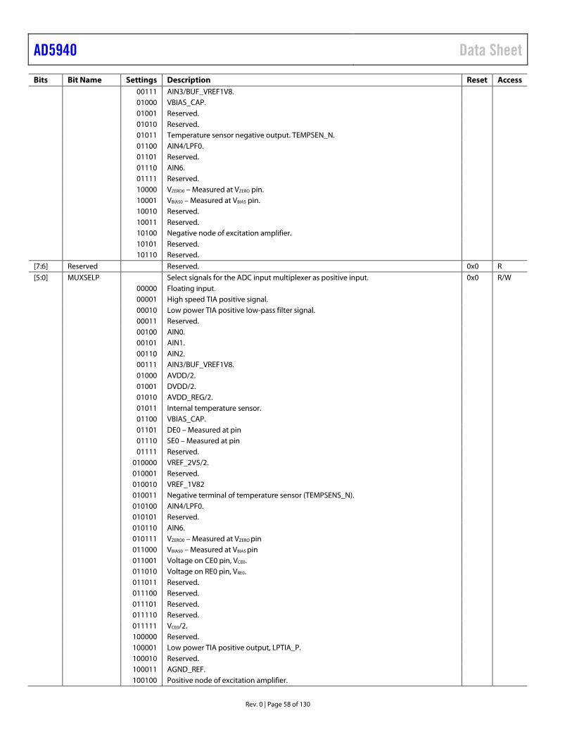
AD5940 Data Sheet
Rev. 0 | Page 58 of 130
Bits Bit Name Settings Description Reset Access 00111 AIN3/BUF_VREF1V8. 01000 VBIAS_CAP. 01001 Reserved. 01010 Reserved. 01011 Temperature sensor negative output. TEMPSEN_N. 01100 AIN4/LPF0. 01101 Reserved. 01110 AIN6. 01111 Reserved. 10000 VZERO0 – Measured at VZERO pin. 10001 VBIAS0 – Measured at VBIAS pin. 10010 Reserved. 10011 Reserved. 10100 Negative node of excitation amplifier. 10101 Reserved. 10110 Reserved.
[7:6] Reserved Reserved. 0x0 R
[5:0] MUXSELP Select signals for the ADC input multiplexer as positive input. 0x0 R/W 00000 Floating input. 00001 High speed TIA positive signal. 00010 Low power TIA positive low-pass filter signal. 00011 Reserved. 00100 AIN0. 00101 AIN1. 00110 AIN2. 00111 AIN3/BUF_VREF1V8. 01000 AVDD/2. 01001 DVDD/2. 01010 AVDD_REG/2. 01011 Internal temperature sensor. 01100 VBIAS_CAP. 01101 DE0 – Measured at pin 01110 SE0 – Measured at pin 01111 Reserved. 010000 VREF_2V5/2. 010001 Reserved. 010010 VREF_1V82 010011 Negative terminal of temperature sensor (TEMPSENS_N). 010100 AIN4/LPF0. 010101 Reserved. 010110 AIN6. 010111 VZERO0 – Measured at VZERO pin 011000 VBIAS0 – Measured at VBIAS pin 011001 Voltage on CE0 pin, VCE0. 011010 Voltage on RE0 pin, VRE0. 011011 Reserved. 011100 Reserved. 011101 Reserved. 011110 Reserved. 011111 VCE0/2. 100000 Reserved. 100001 Low power TIA positive output, LPTIA_P. 100010 Reserved. 100011 AGND_REF. 100100 Positive node of excitation amplifier.
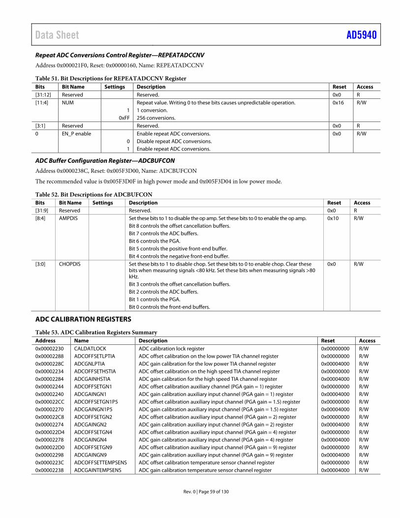
Data Sheet AD5940
Rev. 0 | Page 59 of 130
Repeat ADC Conversions Control Register—REPEATADCCNV
Address 0x000021F0, Reset: 0x00000160, Name: REPEATADCCNV
Table 51. Bit Descriptions for REPEATADCCNV Register Bits Bit Name Settings Description Reset Access [31:12] Reserved Reserved. 0x0 R
[11:4] NUM Repeat value. Writing 0 to these bits causes unpredictable operation. 0x16 R/W 1 1 conversion. 0xFF 256 conversions.
[3:1] Reserved Reserved. 0x0 R
0 EN_P enable Enable repeat ADC conversions. 0x0 R/W 0 Disable repeat ADC conversions. 1 Enable repeat ADC conversions.
ADC Buffer Configuration Register—ADCBUFCON
Address 0x0000238C, Reset: 0x005F3D00, Name: ADCBUFCON
The recommended value is 0x005F3D0F in high power mode and 0x005F3D04 in low power mode.
Table 52. Bit Descriptions for ADCBUFCON Bits Bit Name Settings Description Reset Access [31:9] Reserved Reserved. 0x0 R [8:4] AMPDIS Set these bits to 1 to disable the op amp. Set these bits to 0 to enable the op amp. 0x10 R/W Bit 8 controls the offset cancellation buffers. Bit 7 controls the ADC buffers. Bit 6 controls the PGA. Bit 5 controls the positive front-end buffer. Bit 4 controls the negative front-end buffer. [3:0] CHOPDIS Set these bits to 1 to disable chop. Set these bits to 0 to enable chop. Clear these
bits when measuring signals <80 kHz. Set these bits when measuring signals >80 kHz.
0x0 R/W
Bit 3 controls the offset cancellation buffers. Bit 2 controls the ADC buffers. Bit 1 controls the PGA. Bit 0 controls the front-end buffers.
ADC CALIBRATION REGISTERS
Table 53. ADC Calibration Registers Summary Address Name Description Reset Access 0x00002230 CALDATLOCK ADC calibration lock register 0x00000000 R/W 0x00002288 ADCOFFSETLPTIA ADC offset calibration on the low power TIA channel register 0x00000000 R/W 0x0000228C ADCGNLPTIA ADC gain calibration for the low power TIA channel register 0x00004000 R/W 0x00002234 ADCOFFSETHSTIA ADC offset calibration on the high speed TIA channel register 0x00000000 R/W 0x00002284 ADCGAINHSTIA ADC gain calibration for the high speed TIA channel register 0x00004000 R/W 0x00002244 ADCOFFSETGN1 ADC offset calibration auxiliary channel (PGA gain = 1) register 0x00000000 R/W 0x00002240 ADCGAINGN1 ADC gain calibration auxiliary input channel (PGA gain = 1) register 0x00004000 R/W 0x000022CC ADCOFFSETGN1P5 ADC offset calibration auxiliary input channel (PGA gain = 1.5) register 0x00000000 R/W 0x00002270 ADCGAINGN1P5 ADC gain calibration auxiliary input channel (PGA gain = 1.5) register 0x00004000 R/W 0x000022C8 ADCOFFSETGN2 ADC offset calibration auxiliary input channel (PGA gain = 2) register 0x00000000 R/W 0x00002274 ADCGAINGN2 ADC gain calibration auxiliary input channel (PGA gain = 2) register 0x00004000 R/W 0x000022D4 ADCOFFSETGN4 ADC offset calibration auxiliary input channel (PGA gain = 4) register 0x00000000 R/W 0x00002278 ADCGAINGN4 ADC gain calibration auxiliary input channel (PGA gain = 4) register 0x00004000 R/W 0x000022D0 ADCOFFSETGN9 ADC offset calibration auxiliary input channel (PGA gain = 9) register 0x00000000 R/W 0x00002298 ADCGAINGN9 ADC gain calibration auxiliary input channel (PGA gain = 9) register 0x00004000 R/W 0x0000223C ADCOFFSETTEMPSENS ADC offset calibration temperature sensor channel register 0x00000000 R/W 0x00002238 ADCGAINTEMPSENS ADC gain calibration temperature sensor channel register 0x00004000 R/W
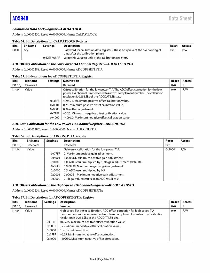
AD5940 Data Sheet
Rev. 0 | Page 60 of 130
Calibration Data Lock Register—CALDATLOCK
Address 0x00002230, Reset: 0x00000000, Name: CALDATLOCK
Table 54. Bit Descriptions for CALDATLOCK Register Bits Bit Name Settings Description Reset Access [31:0] Key Password for calibration data registers. These bits prevent the overwriting of
data after the calibration phase. 0x0 R/W
0xDE87A5AF Write this value to unlock the calibration registers.
ADC Offset Calibration on the Low Power TIA Channel Register—ADCOFFSETLPTIA
Address 0x00002288, Reset: 0x00000000, Name: ADCOFFSETLPTIA
Table 55. Bit descriptions for ADCOFFSETLPTIA Register Bits Bit Name Settings Description Reset Access [31:15] Reserved Reserved. 0x0 R [14:0] Value Offset calibration for the low power TIA. The ADC offset correction for the low
power TIA channel is represented as a twos complement number. The calibration resolution is 0.25 LSBs of the ADCDAT LSB size.
0x0 R/W
0x3FFF 4095.75. Maximum positive offset calibration value. 0x0001 0.25. Minimum positive offset calibration value. 0x0000 0. No offset adjustment. 0x7FFF −0.25. Minimum negative offset calibration value. 0x4000 −4096.0. Maximum negative offset calibration value.
ADC Gain Calibration for the Low Power TIA Channel Register—ADCGNLPTIA
Address 0x0000228C, Reset: 0x00004000, Name: ADCGNLPTIA
Table 56. Bit Descriptions for ADCGNLPTIA Register Bits Bit Name Settings Description Reset Access [31:15] Reserved Reserved. 0x0 R [14:0] Value Gain error calibration for the low power TIA. 0x4000 R/W 0x7FFF 2. Maximum positive gain adjustment. 0x4001 1.000 061. Minimum positive gain adjustment. 0x4000 1.0. ADC result multiplied by 1. No gain adjustment (default). 0x3FFF 0.999939. Minimum negative gain adjustment. 0x2000 0.5. ADC result multiplied by 0.5. 0x0001 0.000061. Maximum negative gain adjustment. 0x0000 0. Illegal value; results in an ADC result of 0.
ADC Offset Calibration on the High Speed TIA Channel Register—ADCOFFSETHSTIA
Address 0x00002234, Reset: 0x00000000, Name: ADCOFFSETHSTIA
Table 57. Bit Descriptions for ADCOFFSETHSTIA Register Bits Bit Name Settings Description Reset Access [31:15] Reserved Reserved. 0x0 R [14:0] Value High speed TIA offset calibration. ADC offset correction for high speed TIA
measurement mode, represented as a twos complement number. The calibration resolution is 0.25 LSBs of the ADCDAT LSB size.
0x0 R/W
0x3FFF 4095.75. Maximum positive offset calibration value. 0x0001 0.25. Minimum positive offset calibration value. 0x0000 0. No offset correction. 0x7FFF −0.25. Minimum negative offset correction. 0x4000 −4096.0. Maximum negative offset correction.
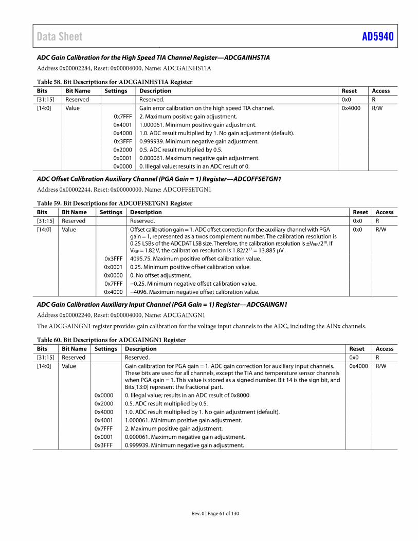
Data Sheet AD5940
Rev. 0 | Page 61 of 130
ADC Gain Calibration for the High Speed TIA Channel Register—ADCGAINHSTIA
Address 0x00002284, Reset: 0x00004000, Name: ADCGAINHSTIA
Table 58. Bit Descriptions for ADCGAINHSTIA Register Bits Bit Name Settings Description Reset Access [31:15] Reserved Reserved. 0x0 R [14:0] Value Gain error calibration on the high speed TIA channel. 0x4000 R/W 0x7FFF 2. Maximum positive gain adjustment. 0x4001 1.000061. Minimum positive gain adjustment. 0x4000 1.0. ADC result multiplied by 1. No gain adjustment (default). 0x3FFF 0.999939. Minimum negative gain adjustment. 0x2000 0.5. ADC result multiplied by 0.5. 0x0001 0.000061. Maximum negative gain adjustment. 0x0000 0. Illegal value; results in an ADC result of 0.
ADC Offset Calibration Auxiliary Channel (PGA Gain = 1) Register—ADCOFFSETGN1
Address 0x00002244, Reset: 0x00000000, Name: ADCOFFSETGN1
Table 59. Bit Descriptions for ADCOFFSETGN1 Register Bits Bit Name Settings Description Reset Access [31:15] Reserved Reserved. 0x0 R [14:0] Value Offset calibration gain = 1. ADC offset correction for the auxiliary channel with PGA
gain = 1, represented as a twos complement number. The calibration resolution is 0.25 LSBs of the ADCDAT LSB size. Therefore, the calibration resolution is ±VREF/218. If VREF = 1.82 V, the calibration resolution is 1.82/217 = 13.885 μV.
0x0 R/W
0x3FFF 4095.75. Maximum positive offset calibration value. 0x0001 0.25. Minimum positive offset calibration value. 0x0000 0. No offset adjustment. 0x7FFF −0.25. Minimum negative offset calibration value. 0x4000 −4096. Maximum negative offset calibration value.
ADC Gain Calibration Auxiliary Input Channel (PGA Gain = 1) Register—ADCGAINGN1
Address 0x00002240, Reset: 0x00004000, Name: ADCGAINGN1
The ADCGAINGN1 register provides gain calibration for the voltage input channels to the ADC, including the AINx channels.
Table 60. Bit Descriptions for ADCGAINGN1 Register Bits Bit Name Settings Description Reset Access [31:15] Reserved Reserved. 0x0 R [14:0] Value Gain calibration for PGA gain = 1. ADC gain correction for auxiliary input channels.
These bits are used for all channels, except the TIA and temperature sensor channels when PGA gain = 1. This value is stored as a signed number. Bit 14 is the sign bit, and Bits[13:0] represent the fractional part.
0x4000 R/W
0x0000 0. Illegal value; results in an ADC result of 0x8000. 0x2000 0.5. ADC result multiplied by 0.5. 0x4000 1.0. ADC result multiplied by 1. No gain adjustment (default). 0x4001 1.000061. Minimum positive gain adjustment. 0x7FFF 2. Maximum positive gain adjustment. 0x0001 0.000061. Maximum negative gain adjustment. 0x3FFF 0.999939. Minimum negative gain adjustment.
AD5940 Data Sheet
Rev. 0 | Page 62 of 130
ADC Offset Calibration Auxiliary Input Channel (PGA Gain = 1.5) Register—ADCOFFSETGN1P5
Address 0x000022CC, Reset: 0x00000000, Name: ADCOFFSETGN1P5
The ADCOFFSETGN1P5 register provides ADC input offset calibration with PGA gain =1.5.
Table 61. Bit Descriptions for ADCOFFSETGN1P5 Register Bits Bit Name Settings Description Reset Access [31:15] Reserved Reserved. 0x0 R [14:0] Value Offset calibration gain = 1.5. ADC offset correction with PGA gain = 1.5. 0x0 R/W 0x3FFF 4095.75. Maximum positive offset calibration value. 0x0001 0.25. Minimum positive offset calibration value. 0x0000 0. No offset adjustment. 0x7FFF −0.25. Minimum negative offset calibration value. 0x4000 −4096. Maximum negative offset calibration value.
ADC Gain Calibration Auxiliary Input Channel (PGA Gain = 1.5) Register—ADCGAINGN1P5
Address 0x00002270, Reset: 0x00004000, Name: ADCGAINGN1P5
The ADCGAINGN1P5 register provides gain calibration for the voltage input channels to the ADC, including the AINx channels.
Table 62. Bit Descriptions for ADCGAINGN1P5 Register Bits Bit Name Settings Description Reset Access [31:15] Reserved Reserved. 0x0 R [14:0] Value Gain calibration for PGA gain = 1.5. These bits provide ADC gain correction for the
auxiliary input channels. These bits are used for all channels except the TIA and temperature sensor channels when PGA gain =1.5. This value is stored as a signed number. Bit 14 is the sign bit and Bits[13:0] represent the fractional part.
0x4000 R/W
0x0000 0. Illegal value resulting in an ADC result of 0. 0x2000 0.5. ADC result multiplied by 0.5. 0x4000 1.0. ADC result multiplied by 1. No gain adjustment (default value). 0x4001 1.000061. Minimum positive gain adjustment. 0x7FFF 2. Maximum positive gain adjustment. 0x0001 0.000061. Maximum negative gain adjustment. 0x3FFF 0.999939. Minimum negative gain adjustment.
ADC Offset Calibration Auxiliary Input Channel (PGA Gain = 2) Register—ADCOFFSETGN2
Address 0x000022C8, Reset: 0x00000000, Name: ADCOFFSETGN2
The ADCOFFSETGN2 register provides ADC input offset calibration with PGA gain = 2
Table 63. Bit Descriptions for ADCOFFSETGN2 Register Bits Bit Name Settings Description Reset Access [31:15] Reserved Reserved. 0x0 R [14:0] Value Offset calibration auxiliary channel (PGA gain = 2). These bits provide ADC offset
correction for inputs using PGA gain = 2, represented as a twos complement number. The calibration resolution is 0.25 LSB of the ADCDAT LSB size. Therefore, the calibration resolution is ±VREF/218. If VREF = 1.82 V, the calibration resolution is 1.8/217 = 13.73 µV.
0x0 R/W
0x3FFF 4095.75. Maximum positive offset calibration value. 0x0001 0.25. Minimum positive offset calibration value. 0x0000 0. No offset adjustment. 0x7FFF −0.25. Minimum negative offset calibration value. 0x4000 −4096. Maximum negative offset calibration value.
Data Sheet AD5940
Rev. 0 | Page 63 of 130
ADC Gain Calibration Auxiliary Input Channel (PGA Gain = 2) Register—ADCGAINGN2
Address 0x00002274, Reset: 0x00004000, Name: ADCGAINGN2
The ADCGAINGN2 register provides gain calibration for the voltage input channels to the ADC, including the AINx channels, when the PGA is enabled with gain = 2.
Table 64. Bit Descriptions for ADCGAINGN2 Register Bits Bit Name Settings Description Reset Access [31:15] Reserved Reserved. 0x0 R [14:0] Value Gain calibration for PGA gain = 2. These bits provide ADC gain correction for the
auxiliary input channels. These bits are used for all channels except the TIA and the temperature sensor channels when PGA gain = 2. This value is stored as a signed number. Bit 14 is the sign bit and Bits[13:0] represent the fractional part.
0x4000 R/W
0x0000 0. Illegal value resulting in an ADC result of 0.0x2000 0.5. ADC result multiplied by 0.5. 0x4000 1.0. ADC result multiplied by 1. No gain adjustment (default value). 0x4001 1.000061. Minimum positive gain adjustment. 0x7FFF 2. Maximum positive gain adjustment.0x0001 0.000061. Maximum negative gain adjustment. 0x3FFF 0.999939. Minimum negative gain adjustment.
ADC Offset Calibration Auxiliary Input Channel (PGA Gain = 4) Register—ADCOFFSETGN4
Address 0x000022D4, Reset: 0x00000000, Name: ADCOFFSETGN4
The ADCOFFSETGN4 register provides ADC input offset calibration with PGA gain = 4.
Table 65. Bit Descriptions for ADCOFFSETGN4 Register Bits Bit Name Settings Description Reset Access [31:15] Reserved Reserved. 0x0 R [14:0] Value 0x0 R/W
0x3FFF 0x0001
Offset calibration gain = 4. ADC offset correction with PGA gain = 4. 4095.75. Maximum positive offset calibration value. 0.25. Minimum positive offset calibration value.
0x0000 0. No offset adjustment.0x7FFF −0.25. Minimum negative offset calibration value. 0x4000 −4096. Maximum negative offset calibration value.
ADC Gain Calibration Auxiliary Input Channel (PGA Gain = 4) Register—ADCGAINGN4
Address 0x00002278, Reset: 0x00004000, Name: ADCGAINGN4
The ADCGAINGN4 register provides gain calibration for the voltage input channels to the ADC, including the AINx channels, when PGA is enabled with gain = 4.
Table 66. Bit Descriptions for ADCGAINGN4 Register Bits Bit Name Settings Description Reset Access [31:15] Reserved Reserved. 0x0 R [14:0] Value Gain calibration for PGA gain = 4. These bits provide ADC gain correction for the
auxiliary input channels. These bits are used for all channels except the TIA and temperature sensor channels when PGA gain = 4. This value is stored as a signed number. Bit 14 is the sign bit and Bits[13:0] represent the fractional part.
0x4000 R/W
0x0000 0. Illegal value resulting in an ADC result of 0.0x2000 0.5. ADC result multiplied by 0.5. 0x4000 1.0. ADC result multiplied by 1. No gain adjustment (default value). 0x4001 1.000061. Minimum positive gain adjustment. 0x7FFF 2. Maximum positive gain adjustment. 0x0001 0.000061. Maximum negative gain adjustment. 0x3FFF 0.999939. Minimum negative gain adjustment.
AD5940 Data Sheet
Rev. 0 | Page 64 of 130
ADC Offset Calibration Auxiliary Input Channel (PGA Gain = 9) Register—ADCOFFSETGN9
Address 0x000022D0, Reset: 0x00000000, Name: ADCOFFSETGN9
The ADCOFFSETGN9 register provides ADC input offset calibration with PGA gain = 9.
Table 67. Bit Descriptions for ADCOFFSETGN9 Register Bits Bit Name Settings Description Reset Access [31:15] Reserved Reserved. 0x0 R [14:0] Value Offset calibration gain = 9. ADC offset correction with PGA gain = 9. 0x0 R/W 0x3FFF 4095.75. Maximum positive offset calibration value. 0x0001 0.25. Minimum positive offset calibration value. 0x0000 0. No offset adjustment. 0x7FFF −0.25. Minimum Negative Offset calibration value. 0x4000 −4096. Maximum Negative Offset calibration value.
ADC Gain Calibration Auxiliary Input Channel (PGA Gain = 9) Register—ADCGAINGN9
Address 0x00002298, Reset: 0x00004000, Name: ADCGAINGN9
The ADCGAINGN9 register provides gain calibration for the voltage input channels to the ADC, including the AINx channels, when the PGA is enabled with gain = 9.
Table 68. Bit Descriptions for ADCGAINGN9 Register Bits Bit Name Settings Description Reset Access [31:15] Reserved Reserved. 0x0 R [14:0] Value Gain calibration for PGA gain = 9. These bits provide ADC gain correction for the
auxiliary input channels. These bits are used for all channels except the TIA and temperature sensor channels when PGA gain = 9. This value is stored as a signed number. Bit 14 is the sign bit and Bits[13:0] represent the fractional part.
0x4000 R/W
0x0000 0. Illegal value resulting in an ADC result of 0. 0x2000 0.5. ADC result multiplied by 0.5. 0x4000 1.0. ADC result multiplied by 1. No gain adjustment (default value). 0x4001 1.000061. Minimum positive gain adjustment. 0x7FFF 2. Maximum positive gain adjustment. 0x0001 0.000061. Maximum negative gain adjustment. 0x3FFF 0.999939. Minimum negative gain adjustment.
ADC Offset Calibration Temperature Sensor Channel Register—ADCOFFSETTEMPSENS
Address 0x0000223C, Reset: 0x00000000, Name: ADCOFFSETTEMPSENS
Table 69. Bit Descriptions for ADCOFFSETTEMPSENS Bits Bit Name Settings Description Reset Access [31:15] Reserved Reserved. 0x0 R [14:0] Value Offset calibration for the temperature sensor. These bits provide ADC offset correction for
the temperature sensor channel, represented as a twos complement number. The calibration resolution is 0.25 LSB of the ADCDAT LSB size. Therefore, the calibration resolution is ±VREF/218. If VREF = 1.82 V, the calibration resolution is: 1.82/217 = 13.73 µV.
0x0 R/W
0x3FFF 4095.75. Maximum positive offset calibration value. 0x0001 0.25. Minimum positive offset calibration value. 0x0000 0. No offset adjustment. 0x7FFF −0.25. Minimum negative offset calibration value. 0x4000 −4096. Maximum negative offset calibration value.
Data Sheet AD5940
Rev. 0 | Page 65 of 130
ADC Gain Calibration Temperature Sensor Channel Register—ADCGAINTEMPSENS
Address 0x00002238, Reset: 0x00004000, Name: ADCGAINTEMPSENS
The ADCGAINTEMPSENS register provides the ADC gain calibration value used when measuring the internal temperature sensor.
Table 70. Bit Descriptions for ADCGAINTEMPSENS Register Bits Bit Name Settings Description Reset Access [31:15] Reserved Reserved. 0x0 R
[14:0] GAINTEMPSENS Gain calibration for the temperature sensor channel. These bits provide ADC gain correction for the temperature sensor channel. This value is stored as a signed number. Bit 14 is the sign bit and Bits[13:0] represent the fractional part.
0x4000 R/W
0x0000 0. Illegal value resulting in an ADC result of 0. 0x2000 0.5. ADC result multiplied by 0.5. 0x4000 1.0. ADC result multiplied by 1. No gain adjustment (default value). 0x4001 1.000061. Minimum positive gain adjustment. 0x7FFF 2. Maximum positive gain adjustment. 0x0001 0.000061. Maximum negative gain adjustment. 0x3FFF 0.999939. Minimum negative gain adjustment.
ADC DIGITAL POSTPROCESSING REGISTERS (OPTIONAL)
Table 71. ADC Digital Postprocessing Registers Summary Address Name Description Reset Access 0x000020A8 ADCMIN ADC minimum value check register 0x00000000 R/W 0x000020AC ADCMINSM ADC minimum hysteresis value register 0x00000000 R/W 0x000020B0 ADCMAX ADC maximum value check register 0x00000000 R/W 0x000020B4 ADCMAXSMEN ADC maximum hysteresis value register 0x00000000 R/W 0x000020B8 ADCDELTA ADC delta value check register 0x00000000 R/W
ADC Minimum Value Check Register—ADCMIN
Address 0x000020A8, Reset: 0x00000000, Name: ADCMIN
Table 72. Bit Descriptions for ADCMIN Register Bits Bit Name Settings Description Reset Access [31:16] Reserved Reserved. 0x0 R
[15:0] MINVAL ADC minimum value threshold. This value is a low ADCDAT threshold value. If a value less than the value of the MINVAL bit is measured by the ADC, the FLAG4 bit in the INTCFLAG0 register or INTCFLAG1 register is set to 1.
0x0 R/W
ADC Minimum Hysteresis Value Register—ADCMINSM
Address 0x000020AC, Reset: 0x00000000, Name: ADCMINSM
Table 73. Bit Descriptions for ADCMINSM Register Bits Bit Name Settings Description Reset Access [31:16] Reserved Reserved. 0x0 R
[15:0] MINCLRVAL ADCMIN hysteresis value. If a value less than ADCMIN is measured by the ADC, the FLAG4 bit in INTCFLAG0 register or INTCFLAG1 register is set. The FLAG4 bit is set until the value of the ADCDAT register is greater than ADCMIN, Bits[15:0] + ADCMINSM, Bits[15:0].
0x0 R/W
ADC Maximum Value Check Register—ADCMAX
Address 0x000020B0, Reset: 0x00000000, Name: ADCMAX
Table 74. Bit Descriptions for ADCMAX Register Bits Bit Name Settings Description Reset Access [31:16] Reserved Reserved. 0x0 R
[15:0] MAXVAL ADC maximum threshold. These bits form the optional maximum ADCDAT threshold. If a value less than ADCMAX is measured by the ADC, the FLAG5 bit in the INTCFLAG0 register or INTCFLAG1 register is set to 1.
0x0 R/W
AD5940 Data Sheet
Rev. 0 | Page 66 of 130
ADC Maximum Hysteresis Value Register—ADCMAXSMEN
Address 0x000020B4, Reset: 0x00000000, Name: ADCMAXSMEN
Table 75. Bit Descriptions for ADCMAXSMEN Register Bits Bit Name Settings Description Reset Access [31:16] Reserved Reserved. 0x0 R [15:0] MAXSWEN ADCMAX hysteresis value. If a value greater than the value of the ADCMAX register is
measured by the ADC, the FLAG5 bit in INTCFLAG0 register or INTCFLAG1 register is set. The FLAG5 bit remains set until the value of the ADCDAT register is less than the value of ADCMAX, Bits[15:0] – ADCMAXSMEN, Bits[15:0].
0x0 R/W
ADC Delta Value Check Register—ADCDELTA
Address 0x000020B8, Reset: 0x00000000, Name: ADCDELTA
Table 76. Bit Descriptions for ADCDELTA Register Bits Bit Name Settings Description Reset Access [31:16] Reserved Reserved. 0x0 R [15:0] DELTAVAL ADCDAT code differences limit option. If two consecutive ADCDAT register results have
a difference greater than ADCDELTA, Bits[15:0], an error flag is set via the FLAG6 bit of the INTCFLAG0 register or INTCFLAG1 register.
0x0 R/W
ADC STATISTICS REGISTERS
Table 77. ADC Statistics Registers Summary Address Name Description Reset Access 0x000021C0 STATSVAR Variance output register 0x00000000 R 0x000021C4 STATSCON Statistics controlmodule configuration register, including mean, variance, and outlier
detection blocks 0x00000000 R/W
0x000021C8 STATSMEAN Mean output register 0x00000000 R
Variance Output Register—STATSVAR
Address 0x000021C0, Reset: 0x00000000, Name: STATSVAR
Table 78. Bit Descriptions for STATSVAR Bits Bit Name Settings Description Reset Access 31 Reserved Reserved. 0x0 R [30:0] Variance Statistical variance value. This value indicates the spread from the mean value. 0x0 R
Statistics Control Register—STATSCON
Address 0x000021C4, Reset: 0x00000000, Name: STATSCON
Table 79. Bit Descriptions for STATSCON Register Bits Bit Name Settings Description Reset Access [31:12] Reserved Reserved. 0x0 R [11:7] STDDEV Standard deviation configuration. 0x0 R/W [6:4] SAMPLENUM Sample size. These bits set the number of ADC samples used for each statistic
calculation. 0x0 R/W
0 128 samples. 1 64 samples.
10 32 samples. 11 16 samples.
100 8 samples. [3:1] Reserved Reserved. 0x0 R/W 0 STATSEN Statistics enable. 0x0 R/W
0 Disable statistics. 1 Enable statistics.

Data Sheet AD5940
Rev. 0 | Page 67 of 130
Statistics Mean Output Register—STATSMEAN
Address 0x000021C8, Reset: 0x00000000, Name: STATSMEAN
Table 80. Bit Descriptions for STATSMEAN Register Bits Bit Name Settings Description Reset Access [31:16] Reserved Reserved. 0x0 R [15:0] Mean Mean output. These bits form the mean value calculated for the number of ADC
samples set by STATSCON, Bits[6:4]. 0x0 R
AD5940 Data Sheet
Rev. 0 | Page 68 of 130
PROGRAMMABLE SWITCH MATRIX The AD5940 provides flexibility for connecting external pins to the high speed DAC excitation amplifier and to the high speed TIA inverting input. This flexibility supports options for impedance measurements of different sensor types and allows an ac signal to be coupled to the dc bias voltage of a sensor.
When configuring the switches, take the switch settings on the output of the low power amplifiers into account.
On power-up, all switches are open to disconnect the sensor.
Figure 32 shows a high level diagram of how each of the switch matrix nodes (data out, positive, negative, and TIA nodes) connect to the internal circuitry of the AD5940. Figure 33 shows a detailed diagram of every switch on the matrix.
SWITCH DESCRIPTIONS Dx/DR0 Switches
The Dx/DR0 switches select the pin to connect to the excitation amplifier output of the high speed DAC. For an impedance measurement, this pin is CE0. The output of the excitation amplifier can be connected to an external calibration resistor (RCAL) via the RCAL0 pin if the DR0 switch is closed.
Px/Pxx Switches
The Px/Pxx switches select the pin to connect to the positive node of the excitation amplifier of the high speed DAC. For most applications, this pin is RE0. The negative input of the excitation amplifier can be connected to an external calibration resistor via the RCAL0 pin if the PR0 switch is closed.
Nx/Nxx Switches
The Nx/Nxx switches select the pin to connect to the negative node of the excitation amplifier of the high speed DAC. The inverting input of the high speed TIA can be connected to an external calibration resistor via the RCAL1 pin if the NR1 switch is closed.
Tx/TR1 Switches
The Tx/TR1 switches select the pin to connect to the inverting input of the high speed TIA. The inverting input of the high speed TIA can be connected to RCAL via the RCAL1 pin if the TR1 switch is closed.
AFEx Switches
The AFE1, AFE2, and AFE3 switches are only intended for use as switches. These switches are not ADC inputs. In a multi-measurement system, these switches provide a method to switch sensor electrodes, which is useful in bioelectric system applications.
RECOMMENDED CONFIGURATION IN HIBERNATE MODE To minimize leakage on the switches connecting to the positive node and negative node of the excitation amplifier, and to minimize leakage on the high speed TIA, it is recommended to tie the switches to the internal 1.82 V LDO generated voltage by closing the PL, PL2, NL, and NL2 switches.
In hibernate mode, it is assumed that only the dc bias voltage from the low power amplifiers is required for the sensor.
OPTIONS FOR CONTROLLING ALL SWITCHES Figure 33 shows all switches connected to the high speed DAC excitation amplifier and to the inverting input of the high speed TIA.
Two options are available for controlling the switches on the switch matrix,
• Control the Tx/TR1, Nx/Nxx, Px/Pxx, and Dx/DR0 switches as a group in the SWCON register.
• Individual control of each switch within the switch matrix using the xSWFULLCON registers.
If controlling the switches using the xSWFULLCON registers, follow this sequence:
1. Write to the specific bit in the xSWFULLCON register. 2. Set the SWSOURCESEL bit in the SWCON register. If this
bit is not set after writing to the xSWFULLCON register, the changes do not take effect.
In addition, status registers are available to read back the open or closed status of each switch.
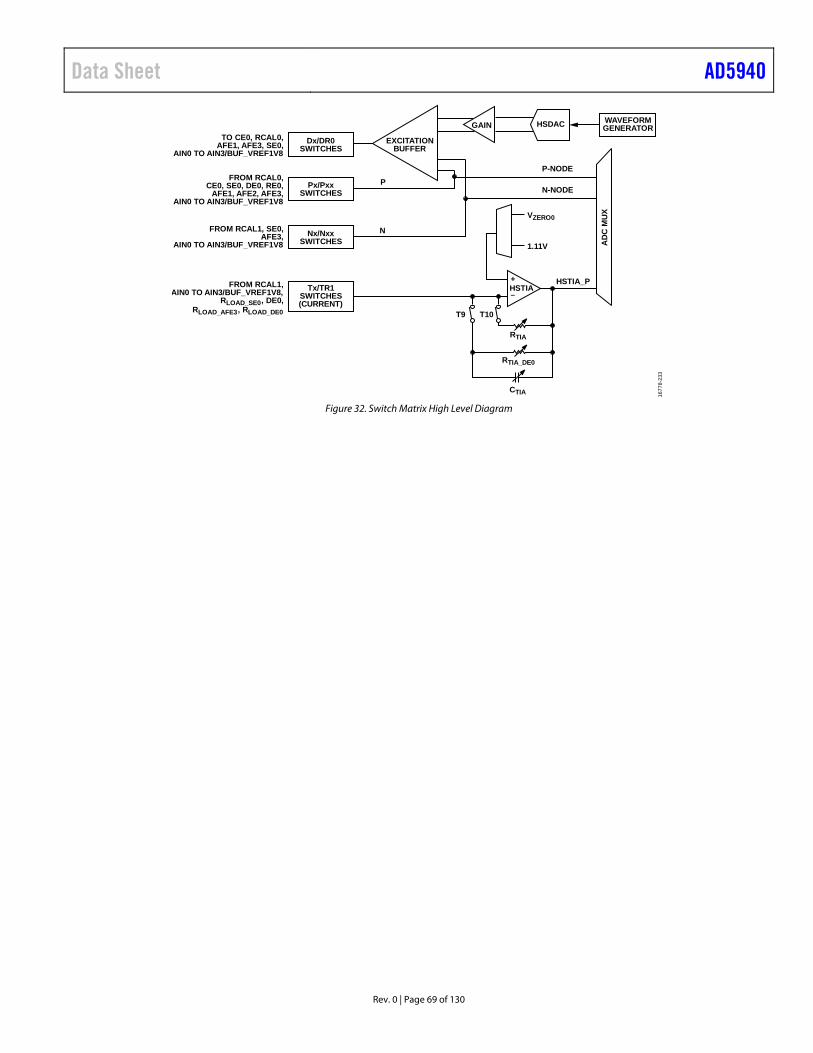
Data Sheet AD5940
Rev. 0 | Page 69 of 130
Dx/DR0SWITCHES
Px/PxxSWITCHES
Nx/NxxSWITCHES
Tx/TR1SWITCHES(CURRENT)
1677
8-23
3
GAIN
EXCITATIONBUFFER
TO CE0, RCAL0,AFE1, AFE3, SE0,
AIN0 TO AIN3/BUF_VREF1V8
FROM RCAL0,CE0, SE0, DE0, RE0,
AFE1, AFE2, AFE3,AIN0 TO AIN3/BUF_VREF1V8
FROM RCAL1, SE0,AFE3,
AIN0 TO AIN3/BUF_VREF1V8
FROM RCAL1,AIN0 TO AIN3/BUF_VREF1V8,
RLOAD_SE0, DE0,RLOAD_AFE3, RLOAD_DE0
HSDAC
VZERO0
P-NODE
N-NODE
AD
C M
UX
1.11V
WAVEFORMGENERATOR
P
N
+HSTIA
T10T9
–
RTIA
RTIA_DE0
CTIA
HSTIA_P
Figure 32. Switch Matrix High Level Diagram
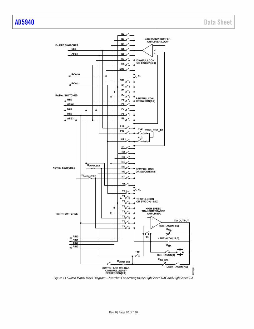
AD5940 Data Sheet
Rev. 0 | Page 70 of 130
AIN0
RCAL0
Dx/DR0 SWITCHES
Px/Pxx SWITCHES
Nx/Nxx SWITCHES
Tx/TR1 SWITCHES
CE0
RE0
RLOAD_DE0
RLOAD_AFE3
RLOAD_SE0
SE0
DE0
AFE3
AFE1
AFE2
RCAL1
+
–RTIA
EXCITATION BUFFERAMPLIFIER LOOP
HIGH SPEEDTRANSIMPEDANCE
AMPLIFIER
CTIA
NR1
TR1
PL
NL
T1
N7
N6
N5
N4
N3
N2
N1
PN
P11
P12
D2
P2
TIA OUTPUT
PR0
N9
RTIA_DE0
T9
T10
PL2
NL2
DVDD_REG_AD
DSWFULLCONOR SWCON[3:0]
PSWFULLCONOR SWCON[7:4]
NSWFULLCONOR SWCON[11:8]
TSWFULLCONOR SWCON[15:12]
HSRTIACON[3:0]
HSRTIACON[12:5]
SWITCH AND RELOADCONTROLLED BYDE0RESCON[7:0]
HSRTIACON[4]
DE0RTIACON[7:0]
AIN1AIN2AIN3
T2
T3
T4
T5
T6
T7
P3
P4
P5
P6
P7
P8
P9
D3
D4
D5
D6
D7
D8
DR0
1677
8-02
4
Figure 33. Switch Matrix Block Diagram—Switches Connecting to the High Speed DAC and High Speed TIA
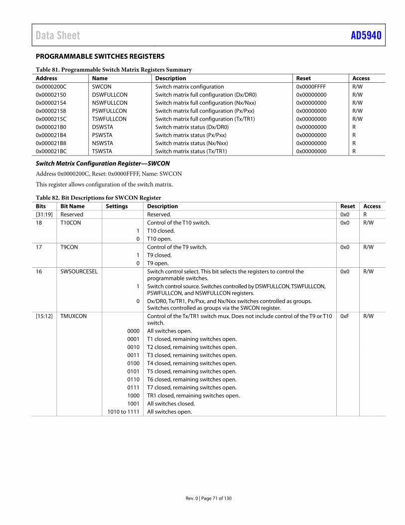
Data Sheet AD5940
Rev. 0 | Page 71 of 130
PROGRAMMABLE SWITCHES REGISTERS
Table 81. Programmable Switch Matrix Registers Summary Address Name Description Reset Access 0x0000200C SWCON Switch matrix configuration 0x0000FFFF R/W 0x00002150 DSWFULLCON Switch matrix full configuration (Dx/DR0) 0x00000000 R/W 0x00002154 NSWFULLCON Switch matrix full configuration (Nx/Nxx) 0x00000000 R/W 0x00002158 PSWFULLCON Switch matrix full configuration (Px/Pxx) 0x00000000 R/W 0x0000215C TSWFULLCON Switch matrix full configuration (Tx/TR1) 0x00000000 R/W 0x000021B0 DSWSTA Switch matrix status (Dx/DR0) 0x00000000 R 0x000021B4 PSWSTA Switch matrix status (Px/Pxx) 0x00000000 R 0x000021B8 NSWSTA Switch matrix status (Nx/Nxx) 0x00000000 R 0x000021BC TSWSTA Switch matrix status (Tx/TR1) 0x00000000 R
Switch Matrix Configuration Register—SWCON
Address 0x0000200C, Reset: 0x0000FFFF, Name: SWCON
This register allows configuration of the switch matrix.
Table 82. Bit Descriptions for SWCON Register Bits Bit Name Settings Description Reset Access [31:19] Reserved Reserved. 0x0 R 18 T10CON Control of the T10 switch. 0x0 R/W 1 T10 closed. 0 T10 open. 17 T9CON Control of the T9 switch. 0x0 R/W 1 T9 closed. 0 T9 open. 16 SWSOURCESEL Switch control select. This bit selects the registers to control the
programmable switches. 0x0 R/W
1 Switch control source. Switches controlled by DSWFULLCON, TSWFULLCON, PSWFULLCON, and NSWFULLCON registers.
0 Dx/DR0, Tx/TR1, Px/Pxx, and Nx/Nxx switches controlled as groups. Switches controlled as groups via the SWCON register.
[15:12] TMUXCON Control of the Tx/TR1 switch mux. Does not include control of the T9 or T10 switch.
0xF R/W
0000 All switches open. 0001 T1 closed, remaining switches open. 0010 T2 closed, remaining switches open. 0011 T3 closed, remaining switches open. 0100 T4 closed, remaining switches open. 0101 T5 closed, remaining switches open. 0110 T6 closed, remaining switches open. 0111 T7 closed, remaining switches open. 1000 TR1 closed, remaining switches open. 1001 All switches closed. 1010 to 1111 All switches open.
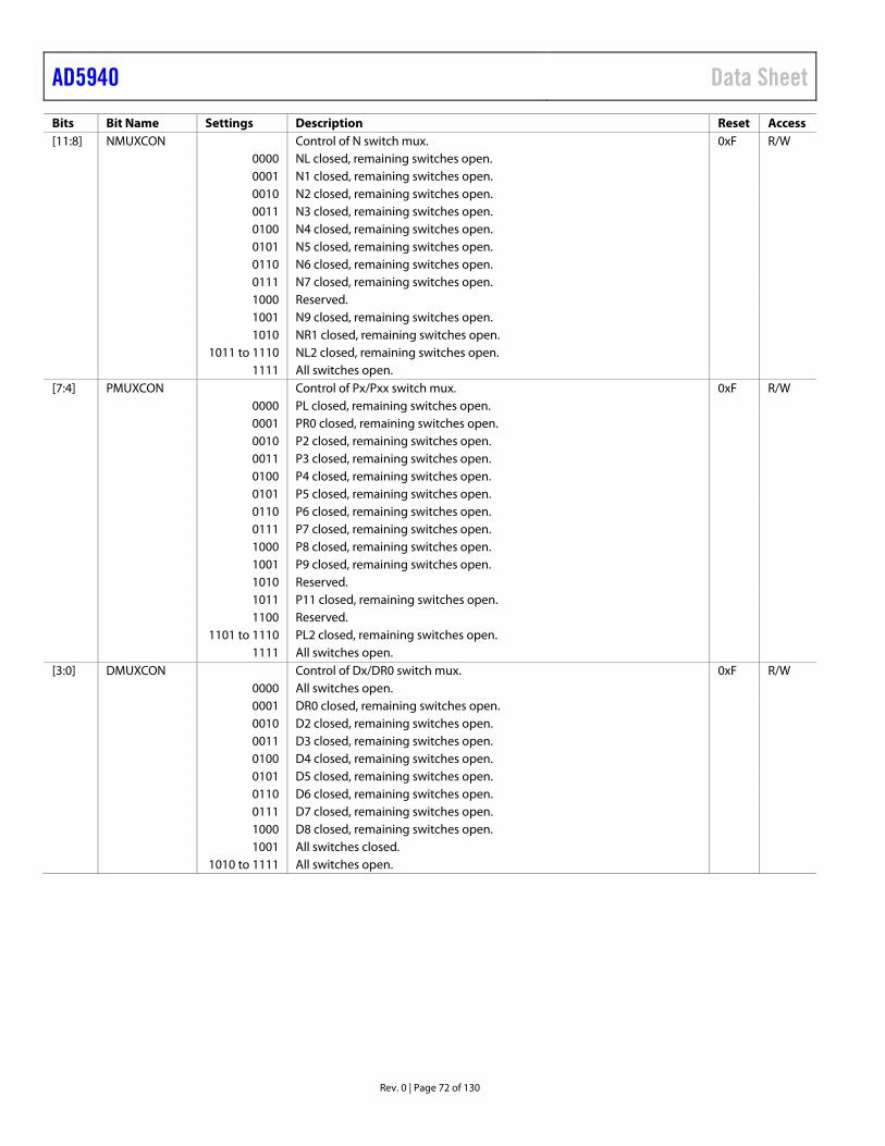
AD5940 Data Sheet
Rev. 0 | Page 72 of 130
Bits Bit Name Settings Description Reset Access [11:8] NMUXCON Control of N switch mux. 0xF R/W 0000 NL closed, remaining switches open. 0001 N1 closed, remaining switches open. 0010 N2 closed, remaining switches open. 0011 N3 closed, remaining switches open. 0100 N4 closed, remaining switches open. 0101 N5 closed, remaining switches open. 0110 N6 closed, remaining switches open. 0111 N7 closed, remaining switches open. 1000 Reserved. 1001 N9 closed, remaining switches open. 1010 NR1 closed, remaining switches open. 1011 to 1110 NL2 closed, remaining switches open. 1111 All switches open. [7:4] PMUXCON Control of Px/Pxx switch mux. 0xF R/W 0000 PL closed, remaining switches open. 0001 PR0 closed, remaining switches open. 0010 P2 closed, remaining switches open. 0011 P3 closed, remaining switches open. 0100 P4 closed, remaining switches open. 0101 P5 closed, remaining switches open. 0110 P6 closed, remaining switches open. 0111 P7 closed, remaining switches open. 1000 P8 closed, remaining switches open. 1001 P9 closed, remaining switches open. 1010 Reserved. 1011 P11 closed, remaining switches open. 1100 Reserved. 1101 to 1110 PL2 closed, remaining switches open. 1111 All switches open. [3:0] DMUXCON Control of Dx/DR0 switch mux. 0xF R/W 0000 All switches open. 0001 DR0 closed, remaining switches open. 0010 D2 closed, remaining switches open. 0011 D3 closed, remaining switches open. 0100 D4 closed, remaining switches open. 0101 D5 closed, remaining switches open. 0110 D6 closed, remaining switches open. 0111 D7 closed, remaining switches open. 1000 D8 closed, remaining switches open. 1001 All switches closed. 1010 to 1111 All switches open.
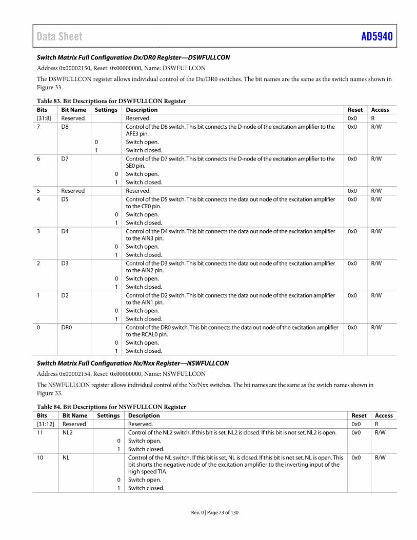
Data Sheet AD5940
Rev. 0 | Page 73 of 130
Switch Matrix Full Configuration Dx/DR0 Register—DSWFULLCON
Address 0x00002150, Reset: 0x00000000, Name: DSWFULLCON
The DSWFULLCON register allows individual control of the Dx/DR0 switches. The bit names are the same as the switch names shown in Figure 33.
Table 83. Bit Descriptions for DSWFULLCON Register Bits Bit Name Settings Description Reset Access [31:8] Reserved Reserved. 0x0 R 7 D8 Control of the D8 switch. This bit connects the D-node of the excitation amplifier to the
AFE3 pin. 0x0 R/W
0 Switch open. 1 Switch closed. 6 D7 Control of the D7 switch. This bit connects the D-node of the excitation amplifier to the
SE0 pin. 0x0 R/W
0 Switch open. 1 Switch closed. 5 Reserved Reserved. 0x0 R/W 4 D5 Control of the D5 switch. This bit connects the data out node of the excitation amplifier
to the CE0 pin. 0x0 R/W
0 Switch open. 1 Switch closed. 3 D4 Control of the D4 switch. This bit connects the data out node of the excitation amplifier
to the AIN3 pin. 0x0 R/W
0 Switch open. 1 Switch closed. 2 D3 Control of the D3 switch. This bit connects the data out node of the excitation amplifier
to the AIN2 pin. 0x0 R/W
0 Switch open. 1 Switch closed. 1 D2 Control of the D2 switch. This bit connects the data out node of the excitation amplifier
to the AIN1 pin. 0x0 R/W
0 Switch open. 1 Switch closed. 0 DR0 Control of the DR0 switch. This bit connects the data out node of the excitation amplifier
to the RCAL0 pin. 0x0 R/W
0 Switch open. 1 Switch closed.
Switch Matrix Full Configuration Nx/Nxx Register—NSWFULLCON
Address 0x00002154, Reset: 0x00000000, Name: NSWFULLCON
The NSWFULLCON register allows individual control of the Nx/Nxx switches. The bit names are the same as the switch names shown in Figure 33.
Table 84. Bit Descriptions for NSWFULLCON Register Bits Bit Name Settings Description Reset Access [31:12] Reserved Reserved. 0x0 R 11 NL2 Control of the NL2 switch. If this bit is set, NL2 is closed. If this bit is not set, NL2 is open. 0x0 R/W 0 Switch open. 1 Switch closed. 10 NL Control of the NL switch. If this bit is set, NL is closed. If this bit is not set, NL is open. This
bit shorts the negative node of the excitation amplifier to the inverting input of the high speed TIA.
0x0 R/W
0 Switch open. 1 Switch closed.
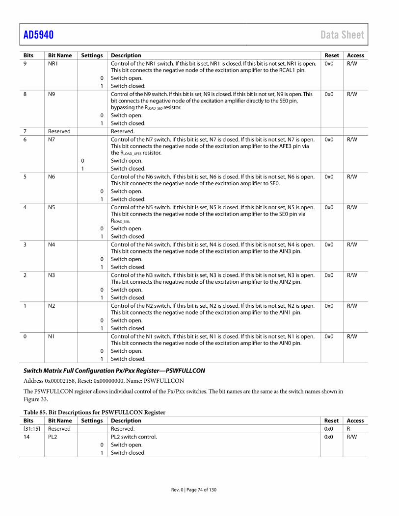
AD5940 Data Sheet
Rev. 0 | Page 74 of 130
Bits Bit Name Settings Description Reset Access 9 NR1 Control of the NR1 switch. If this bit is set, NR1 is closed. If this bit is not set, NR1 is open.
This bit connects the negative node of the excitation amplifier to the RCAL1 pin. 0x0 R/W
0 Switch open. 1 Switch closed. 8 N9 Control of the N9 switch. If this bit is set, N9 is closed. If this bit is not set, N9 is open. This
bit connects the negative node of the excitation amplifier directly to the SE0 pin, bypassing the RLOAD_SE0 resistor.
0x0 R/W
0 Switch open. 1 Switch closed. 7 Reserved Reserved. 6 N7 Control of the N7 switch. If this bit is set, N7 is closed. If this bit is not set, N7 is open.
This bit connects the negative node of the excitation amplifier to the AFE3 pin via the RLOAD_AFE3 resistor.
0x0 R/W
0 Switch open. 1 Switch closed. 5 N6 Control of the N6 switch. If this bit is set, N6 is closed. If this bit is not set, N6 is open.
This bit connects the negative node of the excitation amplifier to SE0. 0x0 R/W
0 Switch open. 1 Switch closed. 4 N5 Control of the N5 switch. If this bit is set, N5 is closed. If this bit is not set, N5 is open.
This bit connects the negative node of the excitation amplifier to the SE0 pin via RLOAD_SE0.
0x0 R/W
0 Switch open. 1 Switch closed. 3 N4 Control of the N4 switch. If this bit is set, N4 is closed. If this bit is not set, N4 is open.
This bit connects the negative node of the excitation amplifier to the AIN3 pin. 0x0 R/W
0 Switch open. 1 Switch closed. 2 N3 Control of the N3 switch. If this bit is set, N3 is closed. If this bit is not set, N3 is open.
This bit connects the negative node of the excitation amplifier to the AIN2 pin. 0x0 R/W
0 Switch open. 1 Switch closed. 1 N2 Control of the N2 switch. If this bit is set, N2 is closed. If this bit is not set, N2 is open.
This bit connects the negative node of the excitation amplifier to the AIN1 pin. 0x0 R/W
0 Switch open. 1 Switch closed. 0 N1 Control of the N1 switch. If this bit is set, N1 is closed. If this bit is not set, N1 is open.
This bit connects the negative node of the excitation amplifier to the AIN0 pin. 0x0 R/W
0 Switch open. 1 Switch closed.
Switch Matrix Full Configuration Px/Pxx Register—PSWFULLCON
Address 0x00002158, Reset: 0x00000000, Name: PSWFULLCON
The PSWFULLCON register allows individual control of the Px/Pxx switches. The bit names are the same as the switch names shown in Figure 33.
Table 85. Bit Descriptions for PSWFULLCON Register Bits Bit Name Settings Description Reset Access [31:15] Reserved Reserved. 0x0 R 14 PL2 PL2 switch control. 0x0 R/W 0 Switch open. 1 Switch closed.
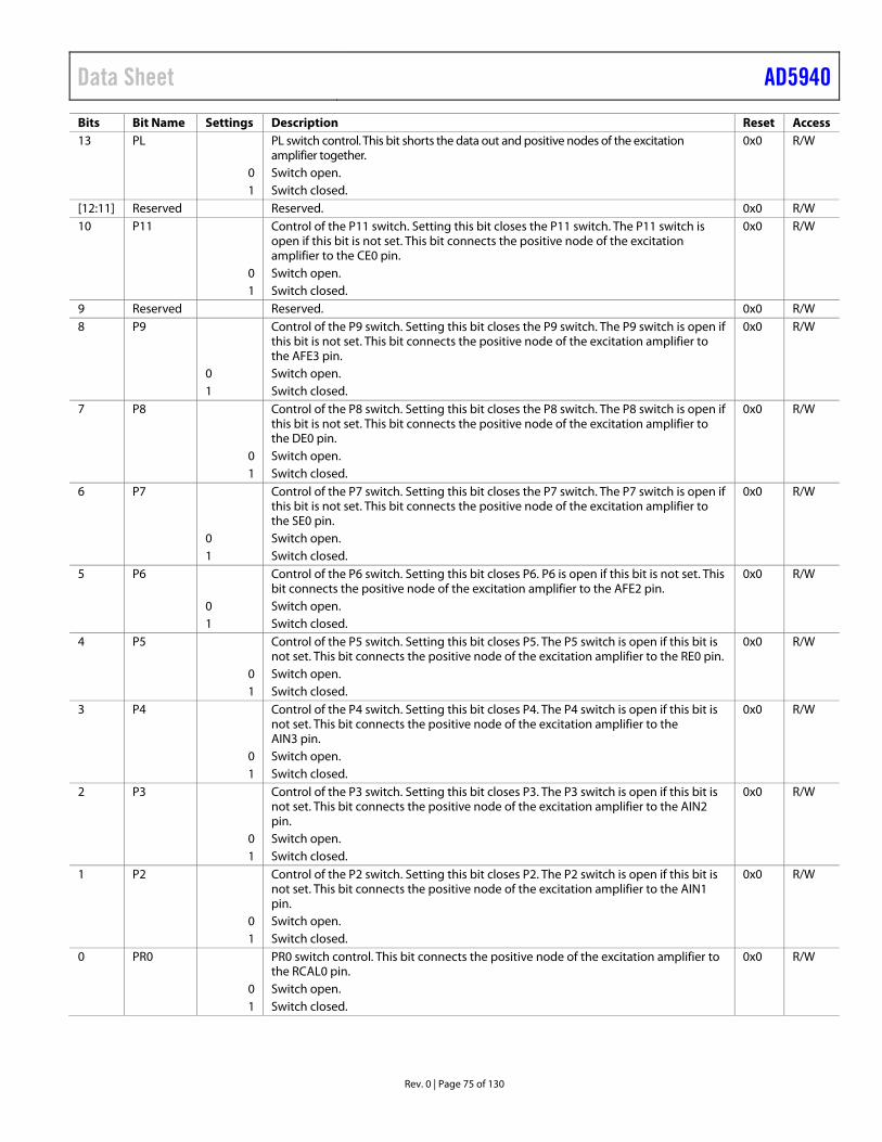
Data Sheet AD5940
Rev. 0 | Page 75 of 130
Bits Bit Name Settings Description Reset Access 13 PL PL switch control. This bit shorts the data out and positive nodes of the excitation
amplifier together. 0x0 R/W
0 Switch open. 1 Switch closed. [12:11] Reserved Reserved. 0x0 R/W 10 P11 Control of the P11 switch. Setting this bit closes the P11 switch. The P11 switch is
open if this bit is not set. This bit connects the positive node of the excitation amplifier to the CE0 pin.
0x0 R/W
0 Switch open. 1 Switch closed. 9 Reserved Reserved. 0x0 R/W 8 P9 Control of the P9 switch. Setting this bit closes the P9 switch. The P9 switch is open if
this bit is not set. This bit connects the positive node of the excitation amplifier to the AFE3 pin.
0x0 R/W
0 Switch open. 1 Switch closed. 7 P8 Control of the P8 switch. Setting this bit closes the P8 switch. The P8 switch is open if
this bit is not set. This bit connects the positive node of the excitation amplifier to the DE0 pin.
0x0 R/W
0 Switch open. 1 Switch closed. 6 P7 Control of the P7 switch. Setting this bit closes the P7 switch. The P7 switch is open if
this bit is not set. This bit connects the positive node of the excitation amplifier to the SE0 pin.
0x0 R/W
0 Switch open. 1 Switch closed. 5 P6 Control of the P6 switch. Setting this bit closes P6. P6 is open if this bit is not set. This
bit connects the positive node of the excitation amplifier to the AFE2 pin. 0x0 R/W
0 Switch open. 1 Switch closed. 4 P5 Control of the P5 switch. Setting this bit closes P5. The P5 switch is open if this bit is
not set. This bit connects the positive node of the excitation amplifier to the RE0 pin. 0x0 R/W
0 Switch open. 1 Switch closed. 3 P4 Control of the P4 switch. Setting this bit closes P4. The P4 switch is open if this bit is
not set. This bit connects the positive node of the excitation amplifier to the AIN3 pin.
0x0 R/W
0 Switch open. 1 Switch closed. 2 P3 Control of the P3 switch. Setting this bit closes P3. The P3 switch is open if this bit is
not set. This bit connects the positive node of the excitation amplifier to the AIN2 pin.
0x0 R/W
0 Switch open. 1 Switch closed. 1 P2 Control of the P2 switch. Setting this bit closes P2. The P2 switch is open if this bit is
not set. This bit connects the positive node of the excitation amplifier to the AIN1 pin.
0x0 R/W
0 Switch open. 1 Switch closed. 0 PR0 PR0 switch control. This bit connects the positive node of the excitation amplifier to
the RCAL0 pin. 0x0 R/W
0 Switch open. 1 Switch closed.
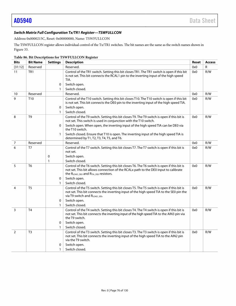
AD5940 Data Sheet
Rev. 0 | Page 76 of 130
Switch Matrix Full Configuration Tx/TR1 Register—TSWFULLCON
Address 0x0000215C, Reset: 0x00000000, Name: TSWFULLCON
The TSWFULLCON register allows individual control of the Tx/TR1 switches. The bit names are the same as the switch names shown in Figure 33.
Table 86. Bit Descriptions for TSWFULLCON Register Bits Bit Name Settings Description Reset Access [31:12] Reserved Reserved. 0x0 R 11 TR1 Control of the TR1 switch. Setting this bit closes TR1. The TR1 switch is open if this bit
is not set. This bit connects the RCAL1 pin to the inverting input of the high speed TIA.
0x0 R/W
0 Switch open. 1 Switch closed. 10 Reserved Reserved. 0x0 R/W 9 T10 Control of the T10 switch. Setting this bit closes T10. The T10 switch is open if this bit
is not set. This bit connects the DE0 pin to the inverting input of the high speed TIA. 0x0 R/W
0 Switch open. 1 Switch closed. 8 T9 Control of the T9 switch. Setting this bit closes T9. The T9 switch is open if this bit is
not set. This switch is used in conjunction with the T10 switch. 0x0 R/W
0 Switch open. When open, the inverting input of the high speed TIA can be DE0 via the T10 switch.
1 Switch closed. Ensure that T10 is open. The inverting input of the high speed TIA is determined by T1, T2, T3, T4, T5, and T6.
7 Reserved Reserved. 0x0 R/W 6 T7 Control of the T7 switch. Setting this bit closes T7. The T7 switch is open if this bit is
not set. 0x0 R/W
0 Switch open. 1 Switch closed. 5 T6 Control of the T6 switch. Setting this bit closes T6. The T6 switch is open if this bit is
not set. This bit allows connection of the RCALx path to the DE0 input to calibrate the RLOAD_DE0 and RTIA_DE0 resistors.
0x0 R/W
0 Switch open. 1 Switch closed. 4 T5 Control of the T5 switch. Setting this bit closes T5. The T5 switch is open if this bit is
not set. This bit connects the inverting input of the high speed TIA to the SE0 pin the via T9 switch and RLOAD_SE0.
0x0 R/W
0 Switch open. 1 Switch closed. 3 T4 Control of the T4 switch. Setting this bit closes T4. The T4 switch is open if this bit is
not set. This bit connects the inverting input of the high speed TIA to the AIN3 pin via the T9 switch.
0x0 R/W
0 Switch open. 1 Switch closed. 2 T3 Control of the T3 switch. Setting this bit closes T3. The T3 switch is open if this bit is
not set. This bit connects the inverting input of the high speed TIA to the AIN2 pin via the T9 switch.
0x0 R/W
0 Switch open. 1 Switch closed.
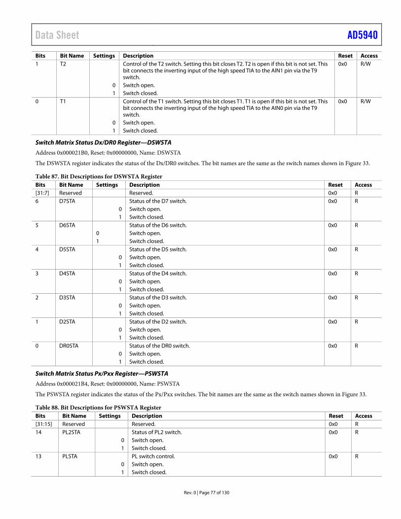
Data Sheet AD5940
Rev. 0 | Page 77 of 130
Bits Bit Name Settings Description Reset Access 1 T2 Control of the T2 switch. Setting this bit closes T2. T2 is open if this bit is not set. This
bit connects the inverting input of the high speed TIA to the AIN1 pin via the T9 switch.
0x0 R/W
0 Switch open. 1 Switch closed. 0 T1 Control of the T1 switch. Setting this bit closes T1. T1 is open if this bit is not set. This
bit connects the inverting input of the high speed TIA to the AIN0 pin via the T9 switch.
0x0 R/W
0 Switch open. 1 Switch closed.
Switch Matrix Status Dx/DR0 Register—DSWSTA
Address 0x000021B0, Reset: 0x00000000, Name: DSWSTA
The DSWSTA register indicates the status of the Dx/DR0 switches. The bit names are the same as the switch names shown in Figure 33.
Table 87. Bit Descriptions for DSWSTA Register Bits Bit Name Settings Description Reset Access [31:7] Reserved Reserved. 0x0 R 6 D7STA Status of the D7 switch. 0x0 R 0 Switch open. 1 Switch closed. 5 D6STA Status of the D6 switch. 0x0 R 0 Switch open. 1 Switch closed. 4 D5STA Status of the D5 switch. 0x0 R 0 Switch open. 1 Switch closed. 3 D4STA Status of the D4 switch. 0x0 R 0 Switch open. 1 Switch closed. 2 D3STA Status of the D3 switch. 0x0 R 0 Switch open. 1 Switch closed. 1 D2STA Status of the D2 switch. 0x0 R 0 Switch open. 1 Switch closed. 0 DR0STA Status of the DR0 switch. 0x0 R 0 Switch open. 1 Switch closed.
Switch Matrix Status Px/Pxx Register—PSWSTA
Address 0x000021B4, Reset: 0x00000000, Name: PSWSTA
The PSWSTA register indicates the status of the Px/Pxx switches. The bit names are the same as the switch names shown in Figure 33.
Table 88. Bit Descriptions for PSWSTA Register Bits Bit Name Settings Description Reset Access [31:15] Reserved Reserved. 0x0 R 14 PL2STA Status of PL2 switch. 0x0 R 0 Switch open. 1 Switch closed. 13 PLSTA PL switch control. 0x0 R 0 Switch open. 1 Switch closed.
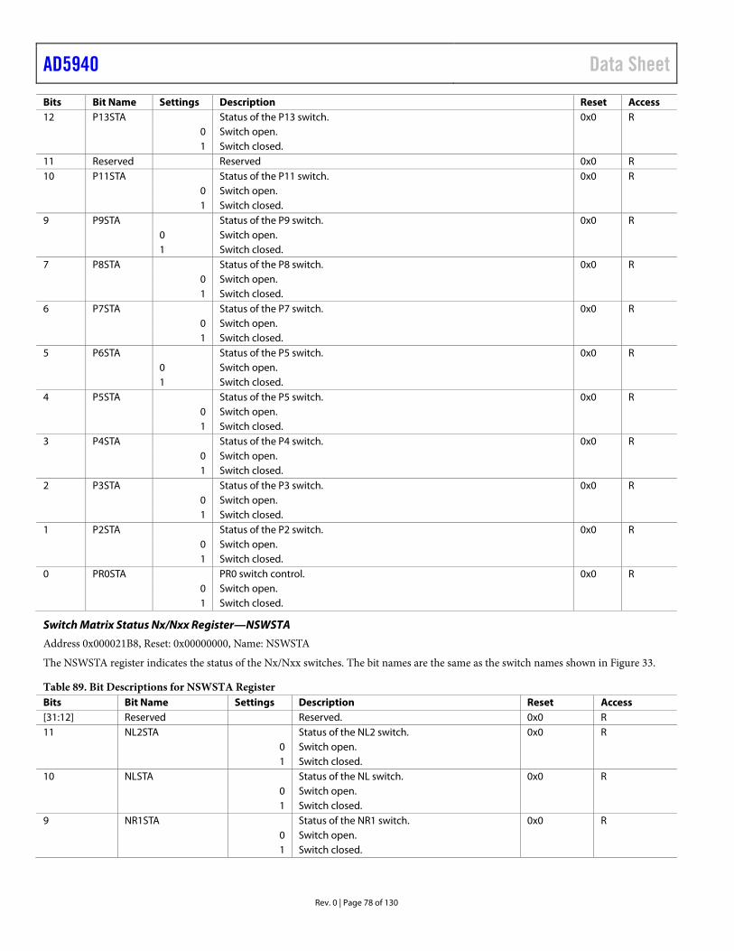
AD5940 Data Sheet
Rev. 0 | Page 78 of 130
Bits Bit Name Settings Description Reset Access 12 P13STA Status of the P13 switch. 0x0 R 0 Switch open. 1 Switch closed. 11 Reserved Reserved 0x0 R 10 P11STA Status of the P11 switch. 0x0 R 0 Switch open. 1 Switch closed. 9 P9STA Status of the P9 switch. 0x0 R 0 Switch open. 1 Switch closed. 7 P8STA Status of the P8 switch. 0x0 R 0 Switch open. 1 Switch closed. 6 P7STA Status of the P7 switch. 0x0 R 0 Switch open. 1 Switch closed. 5 P6STA Status of the P5 switch. 0x0 R 0 Switch open. 1 Switch closed. 4 P5STA Status of the P5 switch. 0x0 R 0 Switch open. 1 Switch closed. 3 P4STA Status of the P4 switch. 0x0 R 0 Switch open. 1 Switch closed. 2 P3STA Status of the P3 switch. 0x0 R 0 Switch open. 1 Switch closed. 1 P2STA Status of the P2 switch. 0x0 R 0 Switch open. 1 Switch closed. 0 PR0STA PR0 switch control. 0x0 R 0 Switch open. 1 Switch closed.
Switch Matrix Status Nx/Nxx Register—NSWSTA
Address 0x000021B8, Reset: 0x00000000, Name: NSWSTA
The NSWSTA register indicates the status of the Nx/Nxx switches. The bit names are the same as the switch names shown in Figure 33.
Table 89. Bit Descriptions for NSWSTA Register Bits Bit Name Settings Description Reset Access [31:12] Reserved Reserved. 0x0 R 11 NL2STA Status of the NL2 switch. 0x0 R 0 Switch open. 1 Switch closed. 10 NLSTA Status of the NL switch. 0x0 R 0 Switch open. 1 Switch closed. 9 NR1STA Status of the NR1 switch. 0x0 R 0 Switch open. 1 Switch closed.
Data Sheet AD5940
Rev. 0 | Page 79 of 130
Bits Bit Name Settings Description Reset Access 8 N9STA Status of the N9 switch. 0x0 R 0 Switch open. 1 Switch closed. 7 Reserved Reserved 0x0 R 6 N7STA Status of the N7 switch. 0x0 R 0 Switch open. 1 Switch closed. 5 N6STA Status of the N6 switch. 0x0 R 0 Switch open. 1 Switch closed. 4 N5STA Status of the N5 switch. 0x0 R 0 Switch open. 1 Switch closed. 3 N4STA Status of the N4 switch. 0x0 R 0 Switch open. 1 Switch closed. 2 N3STA Status of the N3 switch. 0x0 R 0 Switch open. 1 Switch closed. 1 N2STA Status of the N2 switch. 0x0 R 0 Switch open. 1 Switch closed. 0 N1STA Status of the N1 switch. 0x0 R 0 Switch open. 1 Switch closed.
Switch Matrix Status Tx/TR1 Register—TSWSTA
Address 0x000021BC, Reset: 0x00000000, Name: TSWSTA
The TSWSTA register indicates the status of the Tx/TR1 switches. The bit names are the same as the switch names shown in Figure 33.
Table 90. Bit Descriptions for TSWSTA Register Bits Bit Name Settings Description Reset Access [31:12] Reserved Reserved. 0x0 R 11 TR1STA Status of the TR1 switch. 0x0 R 0 Switch open. 1 Switch closed. 10 Reserved Reserved 0x0 R 9 T10STA Status of the T10 switch. 0x0 R 0 Switch open. 1 Switch closed. 8 T9STA Status of the T9 switch. 0x0 R 0 Switch open. 1 Switch closed. 7 Reserved Reserved. 0x0 R 6 T7STA Status of the T7 switch. 0x0 R 0 Switch open. 1 Switch closed. 5 T6STA Status of the T6 switch. 0x0 R 0 Switch open. 1 Switch closed. 4 T5STA Status of the T5 switch. 0x0 R 0 Switch open. 1 Switch closed.
AD5940 Data Sheet
Rev. 0 | Page 80 of 130
Bits Bit Name Settings Description Reset Access 3 T4STA Status of the T4 switch. 0x0 R 0 Switch open. 1 Switch closed. 2 T3STA Status of the T3 switch. 0x0 R 0 Switch open. 1 Switch closed. 1 T2STA Status of the T2 switch. 0x0 R 0 Switch open. 1 Switch closed. 0 T1STA Status of the T1 switch. 0x0 R 0 Switch open. 1 Switch closed.
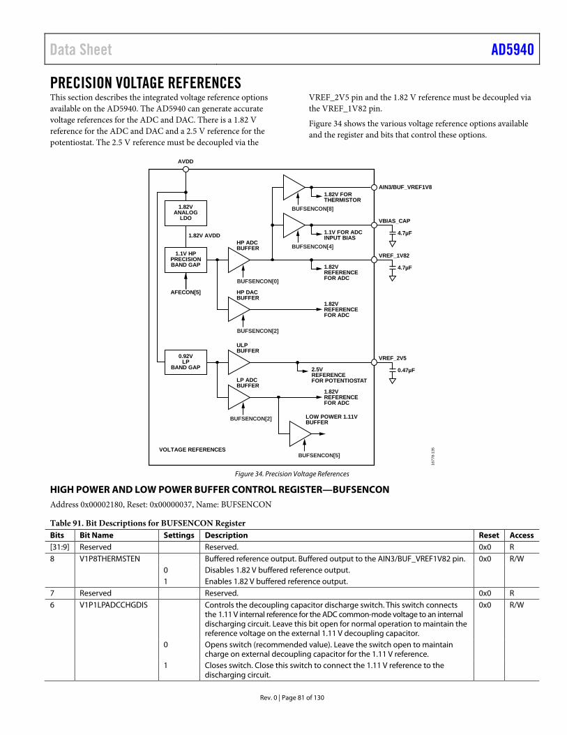
Data Sheet AD5940
Rev. 0 | Page 81 of 130
PRECISION VOLTAGE REFERENCES This section describes the integrated voltage reference options available on the AD5940. The AD5940 can generate accurate voltage references for the ADC and DAC. There is a 1.82 V reference for the ADC and DAC and a 2.5 V reference for the potentiostat. The 2.5 V reference must be decoupled via the
VREF_2V5 pin and the 1.82 V reference must be decoupled via the VREF_1V82 pin.
Figure 34 shows the various voltage reference options available and the register and bits that control these options.
AVDD
BUFSENCON[8]
AIN3/BUF_VREF1V81.82V FORTHERMISTOR
BUFSENCON[4]
VBIAS_CAP
1.1V FOR ADCINPUT BIAS
4.7µF
BUFSENCON[0]
VREF_1V82
1.82VREFERENCEFOR ADC
4.7µF
HP ADCBUFFER
BUFSENCON[2]
1.82VREFERENCEFOR ADC
HP DACBUFFER
VREF_2V5
2.5VREFERENCEFOR POTENTIOSTAT
0.47µF
ULPBUFFER
BUFSENCON[2]
1.82VREFERENCEFOR ADC
LP ADCBUFFER
BUFSENCON[5]
LOW POWER 1.11VBUFFER
1.1V HPPRECISIONBAND GAP
0.92VLP
BAND GAP
1.82VANALOG
LDO
1.82V AVDD
AFECON[5]
VOLTAGE REFERENCES
1677
8-13
5
Figure 34. Precision Voltage References
HIGH POWER AND LOW POWER BUFFER CONTROL REGISTER—BUFSENCON Address 0x00002180, Reset: 0x00000037, Name: BUFSENCON
Table 91. Bit Descriptions for BUFSENCON Register Bits Bit Name Settings Description Reset Access [31:9] Reserved Reserved. 0x0 R 8 V1P8THERMSTEN Buffered reference output. Buffered output to the AIN3/BUF_VREF1V82 pin. 0x0 R/W 0 Disables 1.82 V buffered reference output. 1 Enables 1.82 V buffered reference output. 7 Reserved Reserved. 0x0 R 6 V1P1LPADCCHGDIS Controls the decoupling capacitor discharge switch. This switch connects
the 1.11 V internal reference for the ADC common-mode voltage to an internal discharging circuit. Leave this bit open for normal operation to maintain the reference voltage on the external 1.11 V decoupling capacitor.
0x0 R/W
0 Opens switch (recommended value). Leave the switch open to maintain charge on external decoupling capacitor for the 1.11 V reference.
1 Closes switch. Close this switch to connect the 1.11 V reference to the discharging circuit.
AD5940 Data Sheet
Rev. 0 | Page 82 of 130
Bits Bit Name Settings Description Reset Access 5 V1P1LPADCEN ADC 1.11 V low power common-mode buffer (optional). Use the high speed
or low power reference buffer. 0x1 R/W
0 Disables the 1.11 V low power reference buffer of the ADC. 1 Enables the 1.11 V low power reference buffer of the ADC. 4 V1P1HSADCEN Enables the 1.11 V, high speed, common-mode buffer. This bit controls the
buffer for the 1.11 V common-mode voltage source to the ADC input stage. 0x1 R/W
0 Disables the 1.11 V, high speed, common-mode buffer. 1 Enables the 1.11 V, high speed, common-mode buffer (recommended value
for normal ADC operation).
3 V1P8HSADCCHGDIS Controls the decoupling capacitor discharge switch. This switch connects the 1.82 V internal ADC reference to an internal discharging circuit. Leave this bit open for normal operation to maintain the reference voltage on the external decoupling capacitor.
0x0 R/W
0 Opens switch. If opened, the voltage on the external decoupling capacitor for the reference is maintained (recommended value).
1 Closes switch. Close this switch to connect the reference to the discharge circuit. 2 V1P8LPADCEN ADC 1.82 V low power reference buffer. 0x1 R/W 0 Disables the low power 1.82 V reference buffer. 1 Enables the low power 1.82 V reference buffer (recommended value). This
setting speeds up the settling time when exiting a power-down state.
1 V1P8HSADCILIMITEN High speed ADC input current limit. This bit protects the ADC input buffer. 0x1 R/W 0 Disables buffer current limit. 1 Enables buffer current limit (recommended value). 0 V1P8HSADCEN High speed 1.82 V reference buffer. Enable the reference buffer for normal
ADC conversions. 0x1 R/W
0 Disables 1.82 V high speed ADC reference buffer. 1 Enables 1.82 V high speed ADC reference buffer.
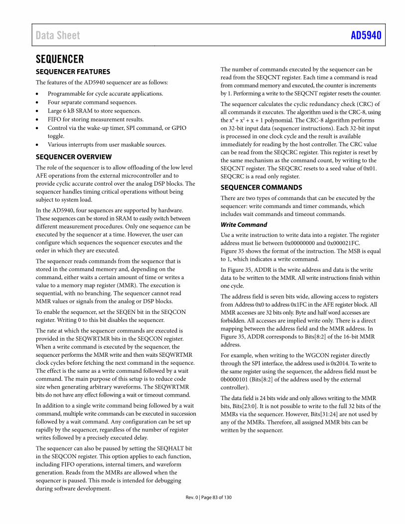
Data Sheet AD5940
Rev. 0 | Page 83 of 130
SEQUENCER SEQUENCER FEATURES The features of the AD5940 sequencer are as follows:
• Programmable for cycle accurate applications. • Four separate command sequences. • Large 6 kB SRAM to store sequences. • FIFO for storing measurement results. • Control via the wake-up timer, SPI command, or GPIO
toggle. • Various interrupts from user maskable sources.
SEQUENCER OVERVIEW The role of the sequencer is to allow offloading of the low level AFE operations from the external microcontroller and to provide cyclic accurate control over the analog DSP blocks. The sequencer handles timing critical operations without being subject to system load.
In the AD5940, four sequences are supported by hardware. These sequences can be stored in SRAM to easily switch between different measurement procedures. Only one sequence can be executed by the sequencer at a time. However, the user can configure which sequences the sequencer executes and the order in which they are executed.
The sequencer reads commands from the sequence that is stored in the command memory and, depending on the command, either waits a certain amount of time or writes a value to a memory map register (MMR). The execution is sequential, with no branching. The sequencer cannot read MMR values or signals from the analog or DSP blocks.
To enable the sequencer, set the SEQEN bit in the SEQCON register. Writing 0 to this bit disables the sequencer.
The rate at which the sequencer commands are executed is provided in the SEQWRTMR bits in the SEQCON register. When a write command is executed by the sequencer, the sequencer performs the MMR write and then waits SEQWRTMR clock cycles before fetching the next command in the sequence. The effect is the same as a write command followed by a wait command. The main purpose of this setup is to reduce code size when generating arbitrary waveforms. The SEQWRTMR bits do not have any effect following a wait or timeout command.
In addition to a single write command being followed by a wait command, multiple write commands can be executed in succession followed by a wait command. Any configuration can be set up rapidly by the sequencer, regardless of the number of register writes followed by a precisely executed delay.
The sequencer can also be paused by setting the SEQHALT bit in the SEQCON register. This option applies to each function, including FIFO operations, internal timers, and waveform generation. Reads from the MMRs are allowed when the sequencer is paused. This mode is intended for debugging during software development.
The number of commands executed by the sequencer can be read from the SEQCNT register. Each time a command is read from command memory and executed, the counter is increments by 1. Performing a write to the SEQCNT register resets the counter.
The sequencer calculates the cyclic redundancy check (CRC) of all commands it executes. The algorithm used is the CRC-8, using the x8 + x2 + x + 1 polynomial. The CRC-8 algorithm performs on 32-bit input data (sequencer instructions). Each 32-bit input is processed in one clock cycle and the result is available immediately for reading by the host controller. The CRC value can be read from the SEQCRC register. This register is reset by the same mechanism as the command count, by writing to the SEQCNT register. The SEQCRC resets to a seed value of 0x01. SEQCRC is a read only register.
SEQUENCER COMMANDS There are two types of commands that can be executed by the sequencer: write commands and timer commands, which includes wait commands and timeout commands.
Write Command
Use a write instruction to write data into a register. The register address must lie between 0x00000000 and 0x000021FC. Figure 35 shows the format of the instruction. The MSB is equal to 1, which indicates a write command.
In Figure 35, ADDR is the write address and data is the write data to be written to the MMR. All write instructions finish within one cycle.
The address field is seven bits wide, allowing access to registers from Address 0x0 to address 0x1FC in the AFE register block. All MMR accesses are 32 bits only. Byte and half word accesses are forbidden. All accesses are implied write only. There is a direct mapping between the address field and the MMR address. In Figure 35, ADDR corresponds to Bits[8:2] of the 16-bit MMR address.
For example, when writing to the WGCON register directly through the SPI interface, the address used is 0x2014. To write to the same register using the sequencer, the address field must be 0b0000101 (Bits[8:2] of the address used by the external controller).
The data field is 24 bits wide and only allows writing to the MMR bits, Bits[23:0]. It is not possible to write to the full 32 bits of the MMRs via the sequencer. However, Bits[31:24] are not used by any of the MMRs. Therefore, all assigned MMR bits can be written by the sequencer.
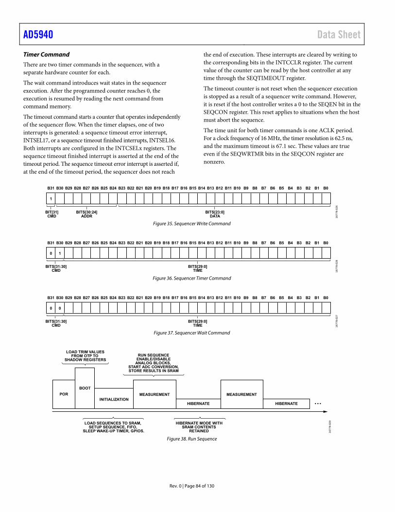
AD5940 Data Sheet
Rev. 0 | Page 84 of 130
Timer Command
There are two timer commands in the sequencer, with a separate hardware counter for each.
The wait command introduces wait states in the sequencer execution. After the programmed counter reaches 0, the execution is resumed by reading the next command from command memory.
The timeout command starts a counter that operates independently of the sequencer flow. When the timer elapses, one of two interrupts is generated: a sequence timeout error interrupt, INTSEL17, or a sequence timeout finished interrupts, INTSEL16. Both interrupts are configured in the INTCSELx registers. The sequence timeout finished interrupt is asserted at the end of the timeout period. The sequence timeout error interrupt is asserted if, at the end of the timeout period, the sequencer does not reach
the end of execution. These interrupts are cleared by writing to the corresponding bits in the INTCCLR register. The current value of the counter can be read by the host controller at any time through the SEQTIMEOUT register.
The timeout counter is not reset when the sequencer execution is stopped as a result of a sequencer write command. However, it is reset if the host controller writes a 0 to the SEQEN bit in the SEQCON register. This reset applies to situations when the host must abort the sequence.
The time unit for both timer commands is one ACLK period. For a clock frequency of 16 MHz, the timer resolution is 62.5 ns, and the maximum timeout is 67.1 sec. These values are true even if the SEQWRTMR bits in the SEQCON register are nonzero.
B31
BIT[31]CMD
BITS[30:24]ADDR
BITS[23:0]DATA
1
B30 B29 B28 B27 B26 B25 B24 B23 B22 B21 B20 B19 B18 B17 B16 B15 B14 B13 B12 B11 B10 B9 B8 B7 B6 B5 B4 B3 B2 B1 B0
1677
8-02
6
Figure 35. Sequencer Write Command
B31
BITS[31:30]CMD
BITS[29:0]TIME
0 1
B30 B29 B28 B27 B26 B25 B24 B23 B22 B21 B20 B19 B18 B17 B16 B15 B14 B13 B12 B11 B10 B9 B8 B7 B6 B5 B4 B3 B2 B1 B0
1677
8-02
8
Figure 36. Sequencer Timer Command
B31
BITS[31:30]CMD
BITS[29:0]TIME
0 0
B30 B29 B28 B27 B26 B25 B24 B23 B22 B21 B20 B19 B18 B17 B16 B15 B14 B13 B12 B11 B10 B9 B8 B7 B6 B5 B4 B3 B2 B1 B0
1677
8-02
7
Figure 37. Sequencer Wait Command
POR
BOOT
INITIALIZATIONMEASUREMENT
HIBERNATE
HIBERNATE MODE WITHSRAM CONTENTS
RETAINED
LOAD SEQUENCES TO SRAM,SETUP SEQUENCE, FIFO,
SLEEP WAKE-UP TIMER, GPIOS.
RUN SEQUENCEENABLE/DISABLE
ANALOG BLOCKS,START ADC CONVERSION,STORE RESULTS IN SRAM
LOAD TRIM VALUESFROM OTP TO
SHADOW REGISTERS
MEASUREMENT
HIBERNATE • • •
1677
8-02
9
Figure 38. Run Sequence
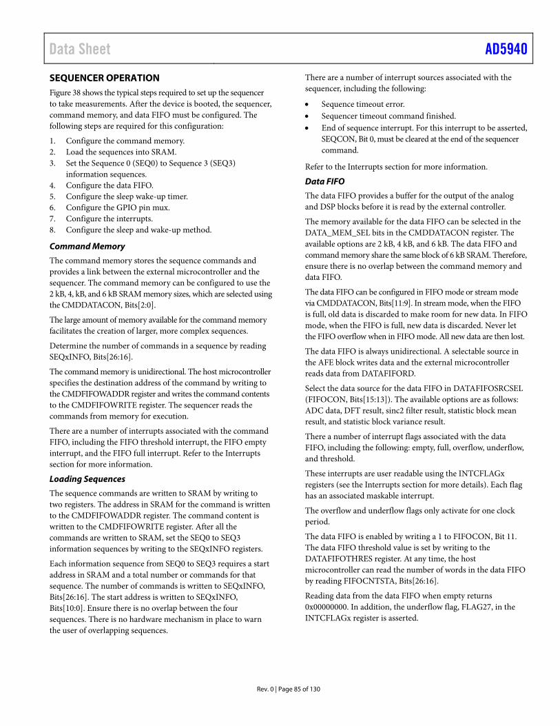
Data Sheet AD5940
Rev. 0 | Page 85 of 130
SEQUENCER OPERATION Figure 38 shows the typical steps required to set up the sequencer to take measurements. After the device is booted, the sequencer, command memory, and data FIFO must be configured. The following steps are required for this configuration:
1. Configure the command memory. 2. Load the sequences into SRAM. 3. Set the Sequence 0 (SEQ0) to Sequence 3 (SEQ3)
information sequences. 4. Configure the data FIFO. 5. Configure the sleep wake-up timer. 6. Configure the GPIO pin mux. 7. Configure the interrupts. 8. Configure the sleep and wake-up method.
Command Memory
The command memory stores the sequence commands and provides a link between the external microcontroller and the sequencer. The command memory can be configured to use the 2 kB, 4, kB, and 6 kB SRAM memory sizes, which are selected using the CMDDATACON, Bits[2:0].
The large amount of memory available for the command memory facilitates the creation of larger, more complex sequences.
Determine the number of commands in a sequence by reading SEQxINFO, Bits[26:16].
The command memory is unidirectional. The host microcontroller specifies the destination address of the command by writing to the CMDFIFOWADDR register and writes the command contents to the CMDFIFOWRITE register. The sequencer reads the commands from memory for execution.
There are a number of interrupts associated with the command FIFO, including the FIFO threshold interrupt, the FIFO empty interrupt, and the FIFO full interrupt. Refer to the Interrupts section for more information.
Loading Sequences
The sequence commands are written to SRAM by writing to two registers. The address in SRAM for the command is written to the CMDFIFOWADDR register. The command content is written to the CMDFIFOWRITE register. After all the commands are written to SRAM, set the SEQ0 to SEQ3 information sequences by writing to the SEQxINFO registers.
Each information sequence from SEQ0 to SEQ3 requires a start address in SRAM and a total number or commands for that sequence. The number of commands is written to SEQxINFO, Bits[26:16]. The start address is written to SEQxINFO, Bits[10:0]. Ensure there is no overlap between the four sequences. There is no hardware mechanism in place to warn the user of overlapping sequences.
There are a number of interrupt sources associated with the sequencer, including the following:
• Sequence timeout error. • Sequencer timeout command finished. • End of sequence interrupt. For this interrupt to be asserted,
SEQCON, Bit 0, must be cleared at the end of the sequencer command.
Refer to the Interrupts section for more information.
Data FIFO
The data FIFO provides a buffer for the output of the analog and DSP blocks before it is read by the external controller.
The memory available for the data FIFO can be selected in the DATA_MEM_SEL bits in the CMDDATACON register. The available options are 2 kB, 4 kB, and 6 kB. The data FIFO and command memory share the same block of 6 kB SRAM. Therefore, ensure there is no overlap between the command memory and data FIFO.
The data FIFO can be configured in FIFO mode or stream mode via CMDDATACON, Bits[11:9]. In stream mode, when the FIFO is full, old data is discarded to make room for new data. In FIFO mode, when the FIFO is full, new data is discarded. Never let the FIFO overflow when in FIFO mode. All new data are then lost.
The data FIFO is always unidirectional. A selectable source in the AFE block writes data and the external microcontroller reads data from DATAFIFORD.
Select the data source for the data FIFO in DATAFIFOSRCSEL (FIFOCON, Bits[15:13]). The available options are as follows: ADC data, DFT result, sinc2 filter result, statistic block mean result, and statistic block variance result.
There a number of interrupt flags associated with the data FIFO, including the following: empty, full, overflow, underflow, and threshold.
These interrupts are user readable using the INTCFLAGx registers (see the Interrupts section for more details). Each flag has an associated maskable interrupt.
The overflow and underflow flags only activate for one clock period.
The data FIFO is enabled by writing a 1 to FIFOCON, Bit 11. The data FIFO threshold value is set by writing to the DATAFIFOTHRES register. At any time, the host microcontroller can read the number of words in the data FIFO by reading FIFOCNTSTA, Bits[26:16].
Reading data from the data FIFO when empty returns 0x00000000. In addition, the underflow flag, FLAG27, in the INTCFLAGx register is asserted.
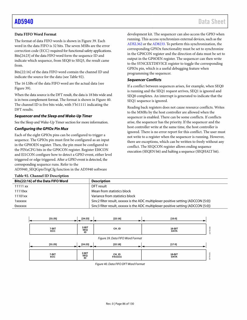
AD5940 Data Sheet
Rev. 0 | Page 86 of 130
Data FIFO Word Format
The format of data FIFO words is shown in Figure 39. Each word in the data FIFO is 32 bits. The seven MSBs are the error correction code (ECC) required for functional safety applications. Bits[24:23] of the data FIFO word form the sequence ID and indicate which sequence, from SEQ0 to SEQ3, the result came from.
Bits[22:16] of the data FIFO word contain the channel ID and indicate the source for the data (see Table 92).
The 16 LSBs of the data FIFO word are the actual data (see Figure 39).
When the data source is the DFT result, the data is 18 bits wide and is in twos complement format. The format is shown in Figure 40. The channel ID is five bits wide, with 5’b11111 indicating the DFT results.
Sequencer and the Sleep and Wake-Up Timer
See the Sleep and Wake-Up Timer section for more information.
Configuring the GPIOx Pin Mux
Each of the eight GPIOx pins can be configured to trigger a sequence. The GPIOx pin must first be configured as an input in the GP0OEN register. Then, the pin must be configured to the PINxCFG bits in the GP0CON register. Register EI0CON and EI1CON configure how to detect a GPIO event, either level triggered or edge triggered. After a GPIO event is detected, the corresponding sequence runs. Refer to the AD5940_SEQGpioTrigCfg function in the AD5940 software
development kit. The sequencer can also access the GPIO when running. This access synchronizes external devices, such as the ADXL362 or the AD8233. To perform this synchronization, the corresponding GPIOx functionality must be set to synchronize in the GP0CON register and the direction of data must be set to output in the GP0OEN register. The sequencer can then write to the SYNCEXTDEVICE register to toggle the corresponding GPIOx pin, which is a useful debugging feature when programming the sequencer.
Sequencer Conflicts
If a conflict between sequences arises, for example, when SEQ0 is running and the SEQ1 request arrives, SEQ1 is ignored and SEQ0 completes. An interrupt is generated to indicate that the SEQ1 sequence is ignored.
Reading back registers does not cause resource conflicts. Writes to the MMRs by the host controller are allowed when the sequencer is enabled. There can be some conflicts. If conflicts arise, the sequencer has the priority. If the sequencer and the host controller write at the same time, the host controller is ignored. There is no error report for this conflict. The user must not write to a register when the sequencer is running. However, there are exceptions, which can be written to freely without any conflict. The SEQCON register allows ending sequence execution (SEQEN bit) and halting a sequence (SEQHALT bit).
Table 92. Channel ID Description Bits[22:16] of the Data FIFO Word Description 11111 xx DFT result 11110xx Mean from statistics block 11101xx Variance from statistics block 1xxxxxx Sinc2 filter result, xxxxxx is the ADC multiplexer positive setting (ADCCON [5:0]) 0xxxxxx Sinc3 filter result, xxxxxx is the ADC multiplexer positive setting (ADCCON [5:0])
[31:25] [24:23] [22:16] [15:0]
7-BITECC
2-BITSEQID
CH_ID 16-BITDATA
1677
8-03
0
Figure 39. Data FIFO Word Format
[31:25] [24:23] [22:18] [17:0]
7-BITECC
2-BITSEQID
CH_ID5'b11111
18-BITDATA
1677
8-03
1
Figure 40. Data FIFO DFT Word Format
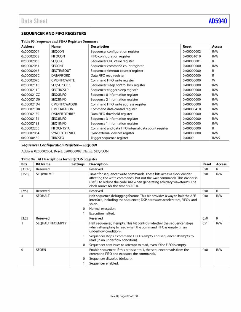
Data Sheet AD5940
Rev. 0 | Page 87 of 130
SEQUENCER AND FIFO REGISTERS
Table 93. Sequence and FIFO Registers Summary Address Name Description Reset Access 0x00002004 SEQCON Sequencer configuration register 0x00000002 R/W 0x00002008 FIFOCON FIFO configuration register 0x00001010 R/W 0x00002060 SEQCRC Sequencer CRC value register 0x00000001 R 0x00002064 SEQCNT Sequencer command count register 0x00000000 R/W 0x00002068 SEQTIMEOUT Sequencer timeout counter register 0x00000000 R 0x0000206C DATAFIFORD Data FIFO read register 0x00000000 R 0x00002070 CMDFIFOWRITE Command FIFO write register 0x00000000 W 0x00002118 SEQSLPLOCK Sequencer sleep control lock register 0x00000000 R/W 0x0000211C SEQTRGSLP Sequencer trigger sleep register 0x00000000 R/W 0x000021CC SEQ0INFO Sequence 0 information register 0x00000000 R/W 0x000021D0 SEQ2INFO Sequence 2 information register 0x00000000 R/W 0x000021D4 CMDFIFOWADDR Command FIFO write address register 0x00000000 R/W 0x000021D8 CMDDATACON Command data control register 0x00000410 R/W 0x000021E0 DATAFIFOTHRES Data FIFO threshold register 0x00000000 R/W 0x000021E4 SEQ3INFO Sequence 3 information register 0x00000000 R/W 0x000021E8 SEQ1INFO Sequence 1 information register 0x00000000 R/W 0x00002200 FIFOCNTSTA Command and data FIFO internal data count register 0x00000000 R 0x00002054 SYNCEXTDEVICE Sync external devices register 0x00000000 R/W 0x00000430 TRIGSEQ Trigger sequence register 0x0000 R/WS
Sequencer Configuration Register—SEQCON
Address 0x00002004, Reset: 0x00000002, Name: SEQCON
Table 94. Bit Descriptions for SEQCON Register Bits Bit Name Settings Description Reset Access [31:16] Reserved Reserved. 0x0 R [15:8] SEQWRTMR Timer for sequencer write commands. These bits act as a clock divider
affecting the write commands, but not the wait commands. This divider is useful to reduce the code size when generating arbitrary waveforms. The clock source for the timer is ACLK.
0x0 R/W
[7:5] Reserved Reserved. 0x0 R 4 SEQHALT Halt sequence debugging feature. This bit provides a way to halt the AFE
interface, including the sequencer, DSP hardware accelerators, FIFOs, and so on.
0x0 R/W
0 Normal execution. 1 Execution halted. [3:2] Reserved Reserved 0x0 R 1 SEQHALTFIFOEMPTY Halt sequencer, if empty. This bit controls whether the sequencer stops
when attempting to read when the command FIFO is empty (in an underflow condition).
0x1 R/W
1 Sequencer stops if command FIFO is empty and sequencer attempts to read (in an underflow condition).
0 Sequencer continues to attempt to read, even if the FIFO is empty. 0 SEQEN Enable sequencer. If this bit is set to 1, the sequencer reads from the
command FIFO and executes the commands. 0x0 R/W
0 Sequencer disabled (default). 1 Sequencer enabled.
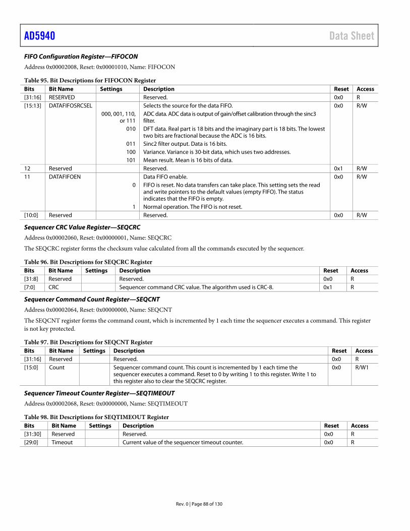
AD5940 Data Sheet
Rev. 0 | Page 88 of 130
FIFO Configuration Register—FIFOCON
Address 0x00002008, Reset: 0x00001010, Name: FIFOCON
Table 95. Bit Descriptions for FIFOCON Register Bits Bit Name Settings Description Reset Access [31:16] RESERVED Reserved. 0x0 R [15:13] DATAFIFOSRCSEL Selects the source for the data FIFO. 0x0 R/W 000, 001, 110,
or 111 ADC data. ADC data is output of gain/offset calibration through the sinc3 filter.
010 DFT data. Real part is 18 bits and the imaginary part is 18 bits. The lowest two bits are fractional because the ADC is 16 bits.
011 Sinc2 filter output. Data is 16 bits. 100 Variance. Variance is 30-bit data, which uses two addresses. 101 Mean result. Mean is 16 bits of data. 12 Reserved Reserved. 0x1 R/W 11 DATAFIFOEN Data FIFO enable. 0x0 R/W 0 FIFO is reset. No data transfers can take place. This setting sets the read
and write pointers to the default values (empty FIFO). The status indicates that the FIFO is empty.
1 Normal operation. The FIFO is not reset. [10:0] Reserved Reserved. 0x0 R/W
Sequencer CRC Value Register—SEQCRC
Address 0x00002060, Reset: 0x00000001, Name: SEQCRC
The SEQCRC register forms the checksum value calculated from all the commands executed by the sequencer.
Table 96. Bit Descriptions for SEQCRC Register Bits Bit Name Settings Description Reset Access [31:8] Reserved Reserved. 0x0 R [7:0] CRC Sequencer command CRC value. The algorithm used is CRC-8. 0x1 R
Sequencer Command Count Register—SEQCNT
Address 0x00002064, Reset: 0x00000000, Name: SEQCNT
The SEQCNT register forms the command count, which is incremented by 1 each time the sequencer executes a command. This register is not key protected.
Table 97. Bit Descriptions for SEQCNT Register Bits Bit Name Settings Description Reset Access [31:16] Reserved Reserved. 0x0 R [15:0] Count Sequencer command count. This count is incremented by 1 each time the
sequencer executes a command. Reset to 0 by writing 1 to this register. Write 1 to this register also to clear the SEQCRC register.
0x0 R/W1
Sequencer Timeout Counter Register—SEQTIMEOUT
Address 0x00002068, Reset: 0x00000000, Name: SEQTIMEOUT
Table 98. Bit Descriptions for SEQTIMEOUT Register Bits Bit Name Settings Description Reset Access [31:30] Reserved Reserved. 0x0 R [29:0] Timeout Current value of the sequencer timeout counter. 0x0 R
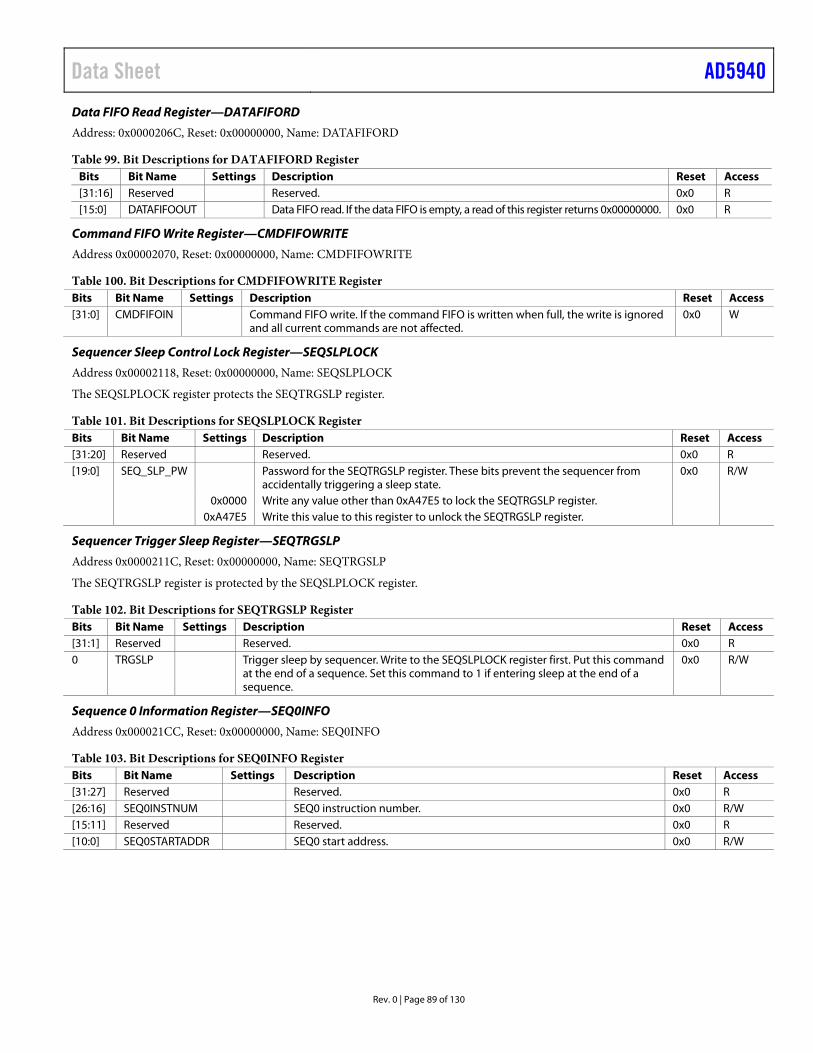
Data Sheet AD5940
Rev. 0 | Page 89 of 130
Data FIFO Read Register—DATAFIFORD
Address: 0x0000206C, Reset: 0x00000000, Name: DATAFIFORD
Table 99. Bit Descriptions for DATAFIFORD Register Bits Bit Name Settings Description Reset Access [31:16] Reserved Reserved. 0x0 R [15:0] DATAFIFOOUT Data FIFO read. If the data FIFO is empty, a read of this register returns 0x00000000. 0x0 R
Command FIFO Write Register—CMDFIFOWRITE
Address 0x00002070, Reset: 0x00000000, Name: CMDFIFOWRITE
Table 100. Bit Descriptions for CMDFIFOWRITE Register Bits Bit Name Settings Description Reset Access [31:0] CMDFIFOIN Command FIFO write. If the command FIFO is written when full, the write is ignored
and all current commands are not affected. 0x0 W
Sequencer Sleep Control Lock Register—SEQSLPLOCK
Address 0x00002118, Reset: 0x00000000, Name: SEQSLPLOCK
The SEQSLPLOCK register protects the SEQTRGSLP register.
Table 101. Bit Descriptions for SEQSLPLOCK Register Bits Bit Name Settings Description Reset Access [31:20] Reserved Reserved. 0x0 R [19:0] SEQ_SLP_PW Password for the SEQTRGSLP register. These bits prevent the sequencer from
accidentally triggering a sleep state. 0x0 R/W
0x0000 Write any value other than 0xA47E5 to lock the SEQTRGSLP register. 0xA47E5 Write this value to this register to unlock the SEQTRGSLP register.
Sequencer Trigger Sleep Register—SEQTRGSLP
Address 0x0000211C, Reset: 0x00000000, Name: SEQTRGSLP
The SEQTRGSLP register is protected by the SEQSLPLOCK register.
Table 102. Bit Descriptions for SEQTRGSLP Register Bits Bit Name Settings Description Reset Access [31:1] Reserved Reserved. 0x0 R 0 TRGSLP Trigger sleep by sequencer. Write to the SEQSLPLOCK register first. Put this command
at the end of a sequence. Set this command to 1 if entering sleep at the end of a sequence.
0x0 R/W
Sequence 0 Information Register—SEQ0INFO
Address 0x000021CC, Reset: 0x00000000, Name: SEQ0INFO
Table 103. Bit Descriptions for SEQ0INFO Register Bits Bit Name Settings Description Reset Access [31:27] Reserved Reserved. 0x0 R [26:16] SEQ0INSTNUM SEQ0 instruction number. 0x0 R/W [15:11] Reserved Reserved. 0x0 R [10:0] SEQ0STARTADDR SEQ0 start address. 0x0 R/W
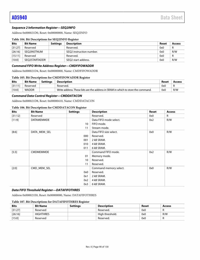
AD5940 Data Sheet
Rev. 0 | Page 90 of 130
Sequence 2 Information Register—SEQ2INFO
Address 0x000021D0, Reset: 0x00000000, Name: SEQ2INFO
Table 104. Bit Descriptions for SEQ2INFO Register Bits Bit Name Settings Description Reset Access [31:27] Reserved Reserved. 0x0 R [26:16] SEQ2INSTNUM SEQ2 instruction number. 0x0 R/W [15:11] Reserved Reserved. 0x0 R [10:0] SEQ2STARTADDR SEQ2 start address. 0x0 R/W
Command FIFO Write Address Register—CMDFIFOWADDR
Address 0x000021D4, Reset: 0x00000000, Name: CMDFIFOWADDR
Table 105. Bit Descriptions for CMDFIFOWADDR Register Bits Bit Name Settings Description Reset Access [31:11] Reserved Reserved. 0x0 R [10:0] WADDR Write address. These bits are the address in SRAM in which to store the command. 0x0 R/W
Command Data Control Register—CMDDATACON
Address 0x000021D8, Reset: 0x00000410, Name: CMDDATACON
Table 106. Bit Descriptions for CMDDATACON Register Bits Bit Name Settings Description Reset Access [31:12] Reserved Reserved. 0x0 R [11:9] DATAMEMMDE Data FIFO mode select. 0x2 R/W 10 FIFO mode. 11 Stream mode. [8:6] DATA_MEM_SEL Data FIFO size select. 0x0 R/W 000 Reserved. 001 2 kB SRAM. 010 4 kB SRAM. 011 6 kB SRAM. [5:3] CMDMEMMDE Command FIFO mode. 0x2 R/W 01 Memory mode. 10 Reserved. 11 Reserved. [2:0] CMD_MEM_SEL Command memory select. 0x0 R/W 0x0 Reserved. 0x1 2 kB SRAM. 0x2 4 kB SRAM. 0x3 6 kB SRAM.
Data FIFO Threshold Register—DATAFIFOTHRES
Address 0x000021E0, Reset: 0x00000000, Name: DATAFIFOTHRES
Table 107. Bit Descriptions for DATAFIFOTHRES Register Bits Bit Name Settings Description Reset Access [31:27] Reserved Reserved. 0x0 R [26:16] HIGHTHRES High threshold. 0x0 R/W [15:0] Reserved Reserved. 0x0 R
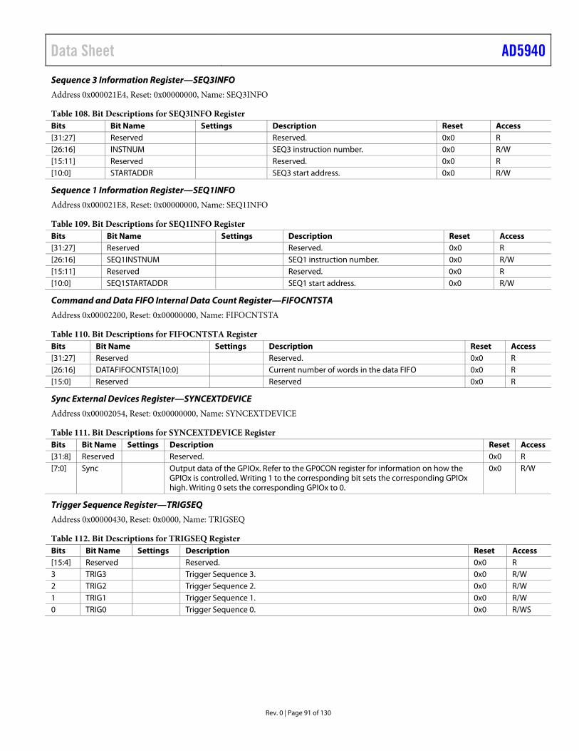
Data Sheet AD5940
Rev. 0 | Page 91 of 130
Sequence 3 Information Register—SEQ3INFO
Address 0x000021E4, Reset: 0x00000000, Name: SEQ3INFO
Table 108. Bit Descriptions for SEQ3INFO Register Bits Bit Name Settings Description Reset Access [31:27] Reserved Reserved. 0x0 R [26:16] INSTNUM SEQ3 instruction number. 0x0 R/W [15:11] Reserved Reserved. 0x0 R [10:0] STARTADDR SEQ3 start address. 0x0 R/W
Sequence 1 Information Register—SEQ1INFO
Address 0x000021E8, Reset: 0x00000000, Name: SEQ1INFO
Table 109. Bit Descriptions for SEQ1INFO Register Bits Bit Name Settings Description Reset Access [31:27] Reserved Reserved. 0x0 R [26:16] SEQ1INSTNUM SEQ1 instruction number. 0x0 R/W [15:11] Reserved Reserved. 0x0 R [10:0] SEQ1STARTADDR SEQ1 start address. 0x0 R/W
Command and Data FIFO Internal Data Count Register—FIFOCNTSTA
Address 0x00002200, Reset: 0x00000000, Name: FIFOCNTSTA
Table 110. Bit Descriptions for FIFOCNTSTA Register Bits Bit Name Settings Description Reset Access [31:27] Reserved Reserved. 0x0 R [26:16] DATAFIFOCNTSTA[10:0] Current number of words in the data FIFO 0x0 R [15:0] Reserved Reserved 0x0 R
Sync External Devices Register—SYNCEXTDEVICE
Address 0x00002054, Reset: 0x00000000, Name: SYNCEXTDEVICE
Table 111. Bit Descriptions for SYNCEXTDEVICE Register Bits Bit Name Settings Description Reset Access [31:8] Reserved Reserved. 0x0 R [7:0] Sync Output data of the GPIOx. Refer to the GP0CON register for information on how the
GPIOx is controlled. Writing 1 to the corresponding bit sets the corresponding GPIOx high. Writing 0 sets the corresponding GPIOx to 0.
0x0 R/W
Trigger Sequence Register—TRIGSEQ
Address 0x00000430, Reset: 0x0000, Name: TRIGSEQ
Table 112. Bit Descriptions for TRIGSEQ Register Bits Bit Name Settings Description Reset Access [15:4] Reserved Reserved. 0x0 R 3 TRIG3 Trigger Sequence 3. 0x0 R/W 2 TRIG2 Trigger Sequence 2. 0x0 R/W 1 TRIG1 Trigger Sequence 1. 0x0 R/W 0 TRIG0 Trigger Sequence 0. 0x0 R/WS
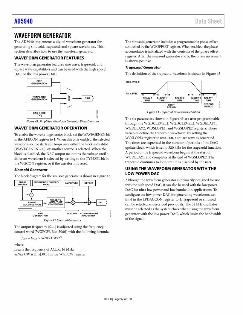
AD5940 Data Sheet
Rev. 0 | Page 92 of 130
WAVEFORM GENERATOR The AD5940 implements a digital waveform generator for generating sinusoid, trapezoid, and square waveforms. This section describes how to use the waveform generator.
WAVEFORM GENERATOR FEATURES The waveform generator features sine wave, trapezoid, and square wave capabilities and can be used with the high speed DAC or the low power DAC.
SINEGENERATION
TRAPEZOIDGENERATION DAC
DAC CODE(DC)
MU
X
1677
8-03
2
Figure 41. Simplified Waveform Generator Block Diagram
WAVEFORM GENERATOR OPERATION To enable the waveform generator block, set the WAVEGENEN bit in the AFECON register to 1. When this bit is enabled, the selected waveform source starts and loops until either the block is disabled (WAVEGENEN = 0), or another source is selected. When the block is disabled, the DAC output maintains the voltage until a different waveform is selected by writing to the TYPESEL bit in the WGCON register, or if the waveform is reset.
Sinusoid Generator
The block diagram for the sinusoid generator is shown in Figure 42.
SINEGENERATION
PHASEACCUMULATOR
PHASE TOAMPLITUDE
CONVERSION
SCALING COMMON-MODEADJUSTMENT
DAC
PHASEOFFSET
AMPLITUDE OFFSETFREQUENCY CONTROLWORD
1677
8-03
3
Figure 42. Sinusoid Generator
The output frequency (fOUT) is adjusted using the frequency control word (WGFCW, Bits[30:0]) with the following formula:
fOUT = fACLK × SINEFCW/230
where: fACLK is the frequency of ACLK, 16 MHz. SINEFCW is Bits[30:0] in the WGFCW register.
The sinusoid generator includes a programmable phase offset controlled by the WGOFFSET register. When enabled, the phase accumulator is initialized with the contents of the phase offset register. After the sinusoid generator starts, the phase increment is always positive.
Trapezoid Generator
The definition of the trapezoid waveform is shown in Figure 43
DC LEVEL 2
DC LEVEL 1
DELAY 1TIME
SLOPE 1TIME
DELAY 2TIME
FIRSTPERIOD
SECONDPERIOD
SLOPE 2TIME
DELAY 1TIME
1677
8-03
4
Figure 43. Trapezoid Waveform Definition
The six parameters shown in Figure 43 are user programmable through the WGDCLEVEL1, WGDCLEVEL2, WGDELAY1, WGDELAY2, WDSLOPE1, and WGSLOPE2 registers. These variables define the trapezoid waveform. By setting the WGSLOPEx register to 0x00000, a square wave is generated. The times are expressed in the number of periods of the DAC update clock, which is set to 320 kHz for the trapezoid function. A period of the trapezoid waveform begins at the start of WGDELAY1 and completes at the end of WGSLOPE2. The trapezoid continues to loop until it is disabled by the user.
USING THE WAVEFORM GENERATOR WITH THE LOW POWER DAC Although the waveform generator is primarily designed for use with the high speed DAC, it can also be used with the low power DAC for ultra low power and low bandwidth applications. To configure the low power DAC for generating waveforms, set Bit 6 in the LPDACCON register to 1. Trapezoid or sinusoid can be selected as described previously. The 32 kHz oscillator must be selected as the system clock when using the waveform generator with the low power DAC, which limits the bandwidth of the signal.
Data Sheet AD5940
Rev. 0 | Page 93 of 130
WAVEFORM GENERATOR REGISTERS
Table 113. Waveform Generator for High Speed DAC Registers Summary Address Name Description Reset Access 0x00002014 WGCON Waveform generator configuration register. 0x00000030 R/W 0x00002018 WGDCLEVEL1 Waveform generator register, Trapezoid DC Level 1. 0x00000000 R/W 0x0000201C WGDCLEVEL2 Waveform generator register, Trapezoid DC Level 2. 0x00000000 R/W 0x00002020 WGDELAY1 Waveform generator register ,Trapezoid Delay 1 time. 0x00000000 R/W 0x00002024 WGSLOPE1 Waveform generator register, Trapezoid Slope 1 time. 0x00000000 R/W 0x00002028 WGDELAY2 Waveform generator register, Trapezoid Delay 2 time. 0x00000000 R/W 0x0000202C WGSLOPE2 Waveform generator register, Trapezoid Slope 2 time. 0x00000000 R/W 0x00002030 WGFCW Waveform generator register, sinusoid frequency control word. 0x00000000 R/W 0x00002034 WGPHASE Waveform generator register, sinusoid phase offset. 0x00000000 R/W 0x00002038 WGOFFSET Waveform generator register, sinusoid offset. 0x00000000 R/W 0x0000203C WGAMPLITUDE Waveform generator register, sinusoid amplitude. 0x00000000 R/W
Waveform Generator Configuration Register—WGCON
Address 0x00002014, Reset: 0x00000030, Name: WGCON
Table 114. Bit Descriptions for WGCON Register Bits Bit Name Settings Description Reset Access [31:6] Reserved Reserved 0x0 R 5 DACGAINCAL Bypass DAC gain. Use the DAC gain calculated during the Analog Devices
factory trim and stored in the DACGAIN register. 0x1 R/W
0 Bypass DAC gain correction. 1 Perform DAC gain correction. 4 DACOFFSETCAL Bypass DAC Offset. Use the DAC offset calculated during the calibration routine. 0x1 R/W 0 Bypass DAC offset correction. 1 Perform DAC offset correction. The offset value is in the DACOFFSET register and
the DACOFFSETHS register for low power and high power mode, respectively, when LPDACCON0, Bit 0 = 0. The offset value is in the DACOFFSETATTEN register and the DACOFFSETATTENHS register for low power and high power mode, respectively, when LPDACCON0, Bit 0 = 1.
3 Reserved Reserved. 0x0 R [2:1] TYPESEL These bits select the type of waveform. 0x0 R/W 00 Direct write to the DAC. User code writes to the HSDACDAT register directly. 10 Sinusoid. Sets the WAVEGENEN bit in the AFECON register to 1. The DAC outputs
a sine wave.
11 Trapezoid. Sets the WAVEGENEN bit in the AFECON register to 1. The DAC outputs a trapezoid wave.
0 TRAPRSTEN Resets the trapezoid waveform generator. The output restarts from the beginning of the Delay 1 period, with an output corresponding to DC Level 1. The reset takes effect immediately. After the trapezoid generator is reset, the bit value returns to 0.
0x0 W
0 Disable reset of the trapezoid waveform generator. 1 Enable reset of the trapezoid waveform generator.
Waveform Generator, Trapezoid DC Level 1 Register—WGDCLEVEL1
Address 0x00002018, Reset: 0x00000000, Name: WGDCLEVEL1
Table 115. Bit Descriptions for WGDCLEVEL1 Register Bits Bit Name Settings Description Reset Access [31:12] Reserved Reserved. 0x0 R [11:0] TRAPDCLEVEL1 DC Level 1 value for trapezoid waveform generation. 0x0 R/W
AD5940 Data Sheet
Rev. 0 | Page 94 of 130
Waveform Generator, Trapezoid DC Level 2 Register—WGDCLEVEL2
Address 0x0000201C, Reset: 0x00000000, Name: WGDCLEVEL2
Table 116. Bit Descriptions for WGDCLEVEL2 Register Bits Bit Name Settings Description Reset Access [31:12] Reserved Reserved. 0x0 R [11:0] TRAPDCLEVEL2 DC Level 2 value for trapezoid waveform generation. 0x0 R/W
Waveform Generator, Trapezoid Delay 1 Time Register—WGDELAY1
Address 0x00002020, Reset: 0x00000000, Name: WGDELAY1
Table 117. Bit Descriptions for WGDELAY1 Register Bits Bit Name Settings Description Reset Access [31:20] Reserved Reserved. 0x0 R [19:0] DELAY1 Delay 1 value for trapezoid waveform generation. The unit of time is the DAC
update rate. 0x0 R/W
Waveform Generator, Trapezoid Slope 1 Time Register—WGSLOPE1
Address 0x00002024, Reset: 0x00000000, Name: WGSLOPE1
Table 118. Bit Descriptions for WGSLOPE1 Register Bits Bit Name Settings Description Reset Access [31:20] Reserved Reserved. 0x0 R [19:0] SLOPE1 Slope 1 value for trapezoid waveform generation. The unit of time is the DAC update
rate. For trapezoid generation, the DAC update rate is fixed to 320 kHz. 0x0 R/W
Waveform Generator, Trapezoid Delay 2 Time Register—WGDELAY2
Address 0x00002028, Reset: 0x00000000, Name: WGDELAY2
Table 119. Bit Descriptions for WGDELAY2 Register Bits Bit Name Settings Description Reset Access [31:20] Reserved Reserved. 0x0 R [19:0] DELAY2 Delay 2 value for trapezoid waveform generation. The unit of time is the DAC
update rate. For trapezoid generation, the DAC update rate is fixed to 320 kHz. 0x0 R/W
Waveform Generator, Trapezoid Slope 2 Time Register—WGSLOPE2
Address 0x0000202C, Reset: 0x00000000, Name: WGSLOPE2
Table 120. Bit Descriptions for WGSLOPE2 Register Bits Bit Name Settings Description Reset Access [31:20] Reserved Reserved. 0x0 R [19:0] SLOPE2 Slope 2 value for trapezoid waveform generation. The unit of time is the DAC update
rate. For trapezoid generation, the DAC update rate is fixed to 320 kHz. 0x0 R/W
Data Sheet AD5940
Rev. 0 | Page 95 of 130
Waveform Generator, Sinusoid Frequency Control Word Register—WGFCW
Address 0x00002030, Reset: 0x00000000, Name: WGFCW
Table 121. Bit Descriptions for WGFCW Register Bits Bit Name Settings Description Reset Access [31:24] Reserved Reserved. 0x0 R [30:0] SINEFCW Sinusoid generator frequency control word. These bits select the output frequency
of the sinusoid waveform. The output frequency (fOUT) = fACLK × (SINEFCW/230). To obtain accurate DFT results and to avoid spectral leakage, fOUT/(DFT input data rate/N) must be an integer, where N is input data number of DFT. Refer to the DFTNUM bit in the DFTCON register (see Table 48). The DFT input data rate can be different due to different input data sources. Refer to the DFTINSEL bit in the DFTCON register (see Table 48). Sinc3 is output as input data of DFT (the DFT input data rate = ADC output data rate(1.6 MHz or 800 kHz)/SINC3_OSR)). Refer to the SINC3OSR bit in the ADCFILTERCON register (see Table 42). For the sinc3 bypass, refer to the SINC3BYP bit in the ADCFILTERCON register (see Table 42). If the DFT input data rate = 800 kHz, the ADC output data rate must be set to 800 kHz. Refer to the ADCSAMPLERATE bit in the ADCFILTERCON register = 1 (see Table 42). The general formula is ADC_FS/SINC3_OSR/SINC2_OS. Refer to the SINC2OSR bit in the ADCFILTERCON register (see Table 42). For more information, see the High Performance ADC Circuit section.
0x0 R/W
Waveform Generator, Sinusoid Phase Offset Register—WGPHASE
Address 0x00002034, Reset: 0x00000000, Name: WGPHASE
Table 122. Bit Descriptions for WGPHASE Register Bits Bit Name Settings Description Reset Access [31:20] Reserved Reserved. 0x0 R [19:0] SINEOFFSET Sinusoid phase offset. SINEOFFSET, Bits[19:0] = phase (degrees)/360 × 220. For
example, to obtain a 45° phase offset, SINEOFFSET, Bits[19:0] = 45/360 × 220. This register must be set before setting the TYPESEL bit in the WGCON register and the WAVEGENEN bit in the AFECON register.
0x0 R/W
Waveform Generator, Sinusoid Offset Register—WGOFFSET
Address 0x00002038, Reset: 0x00000000, Name: WGOFFSET
Table 123. Bit Descriptions for WGOFFSET Register Bits Bit Name Settings Description Reset Access [31:12] Reserved Reserved. 0x0 R [11:0] SINEOFFSET Sinusoid offset. This offset is added to the waveform generator output in sinusoid
mode. This value is a signed number represented in twos complement format. This register must be set before setting the TYPESEL bit in the WGCON register and the WAVEGENEN bit in the AFECON register.
0x0 R/W
Waveform Generator, Sinusoid Amplitude Register—WGAMPLITUDE
Address 0x0000203C, Reset: 0x00000000, Name: WGAMPLITUDE
Table 124. Bit Descriptions for WGAMPLITUDE Register Bits Bit Name Settings Description Reset Access [31:11] Reserved Reserved. 0x0 R [10:0] SINEAMPLITUDE Sinusoid amplitude, unsigned number. This amplitude scales the waveform
generator in sinusoid mode. The DAC output voltage is determined by this value, as well as the ATTENEN bit and the INAMPGNMDE bit in the HSDACCON register. This register must be set before setting the TYPESEL bit in the WGCON register and the WAVEGENEN bit in the AFECON register.
0x0 R/W
AD5940 Data Sheet
Rev. 0 | Page 96 of 130
SPI INTERFACE OVERVIEW The AD5940 provides an SPI interface to facilitate configuration and control by a host microcontroller. The host controller uses the SPI to read from and write to memory, registers, and FIFOs. The AD5940 operate as a slave SPI device.
SPI PINS
The SPI connections between the host and the AD5940 are CS, SCLK, MOSI, and MISO.
Chip Select Enable
The host must connect the SPI slave enable signal to the CS input of the AD5940. To initiate an SPI transaction, the host drives the CS signal low before the first SCLK rising edge and drives it high again after the last SCLK falling edge. The AD5940 ignores the SCLK and MOSI signals of the SPI when the CS input is high.
SCLK
SCLK is the serial clock driven by the host to the AD5940. The maximum clock speed is 16 MHz.
MOSI and MISO
MOSI is the data input line driven from the host to the AD5940, and MISO is the data output from the AD5940 to the host. The MOSI signal and MISO signal are launched on the falling edge of the SCLK signal and sampled on the rising edge of the SCLK signal by the host and the AD5940, respectively. The MOSI signal carries the data from the host to the AD5940. The MISO signal carries the returning read data fields from the AD5940 to the host during a read transaction.
SPI OPERATION The host is the master of the SPI. The features and requirements of SPI operation are as follows:
• SCLK is always slower than the system clock on the AD5940, which is 16 MHz.
• When the CS signal is brought low, a multiple of eight clock cycles must be generated by the host.
• Transfers over the SPI slave are always byte aligned. • In every octet, the most significant bit (Bit 7) is transmitted
and received first. • If the CS signal is brought high at any time by the host, the
AD5940 is ready to accept new SPI transactions when the CS signal is brought low again by the host. The minimum time between CS going high and going low again is t10 (see Table 4).
COMMAND BYTE The first byte sent from the host to the AD5940 in an SPI transaction is the command byte. The command byte specifies the SPI protocol used for the SPI transaction. The available commands are detailed in Table 125.
Table 125. SPI Commands Command Value Description SPICMD_SETADDR 0x20 Set register address for SPI
transaction SPICMD_READREG 0x6D Specifies SPI transaction is a read
transaction SPICMD_WRITEREG 0x2D Specifies SPI transaction is a write
transaction SPICMD_READFIFO 0x5F Command to read FIFO
Two main SPI transaction protocols are available on the AD5940: writing to and reading from registers and reading data from the data FIFO.
WRITING TO AND READING FROM REGISTERS Writing to and reading from a register requires two SPI transactions. The first transaction sets the register address. The second transaction is the actual read or write to the required register. The following are the steps to write to a register:
1. Write the command byte and configure the register address. a. Drive CS low. b. Send 8-bit command byte: SPICMD_SETADDR. c. Send 16-bit address of register to read to or write
from. d. Pull CS high.
2. Write the data to the register. a. Drive CS low. b. Send 8-bit command byte: SPICMD_WRITEREG. c. Write either 16-bit or 32-bit data to the register. d. Bring CS high.
3. Read the data from the register. a. Drive CS low. b. Send 8-bit command byte: SPICMD_READREG. c. Transmit a dummy byte on the SPI bus to initiate a
read. d. Read returning 16-bit or 32-bit data. e. Bring CS high.
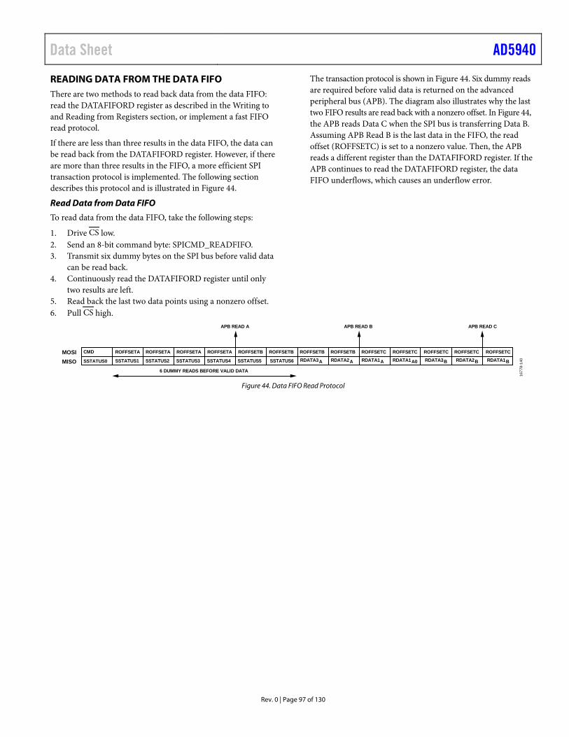
Data Sheet AD5940
Rev. 0 | Page 97 of 130
READING DATA FROM THE DATA FIFO There are two methods to read back data from the data FIFO: read the DATAFIFORD register as described in the Writing to and Reading from Registers section, or implement a fast FIFO read protocol.
If there are less than three results in the data FIFO, the data can be read back from the DATAFIFORD register. However, if there are more than three results in the FIFO, a more efficient SPI transaction protocol is implemented. The following section describes this protocol and is illustrated in Figure 44.
Read Data from Data FIFO
To read data from the data FIFO, take the following steps:
1. Drive CS low. 2. Send an 8-bit command byte: SPICMD_READFIFO. 3. Transmit six dummy bytes on the SPI bus before valid data
can be read back. 4. Continuously read the DATAFIFORD register until only
two results are left. 5. Read back the last two data points using a nonzero offset. 6. Pull CS high.
The transaction protocol is shown in Figure 44. Six dummy reads are required before valid data is returned on the advanced peripheral bus (APB). The diagram also illustrates why the last two FIFO results are read back with a nonzero offset. In Figure 44, the APB reads Data C when the SPI bus is transferring Data B. Assuming APB Read B is the last data in the FIFO, the read offset (ROFFSETC) is set to a nonzero value. Then, the APB reads a different register than the DATAFIFORD register. If the APB continues to read the DATAFIFORD register, the data FIFO underflows, which causes an underflow error.
MOSIMISO
CMD
SSTATUS0
ROFFSETA
SSTATUS1
ROFFSETA
SSTATUS2
ROFFSETA
SSTATUS3
ROFFSETA
SSTATUS4
ROFFSETB
SSTATUS5 SSTATUS6
ROFFSETB ROFFSETBRDATA3A
ROFFSETBRDATA2A
ROFFSETCRDATA1A
ROFFSETC ROFFSETC ROFFSETC ROFFSETC
APB READ A
6 DUMMY READS BEFORE VALID DATA
APB READ B APB READ C
RDATA1A0 RDATA3B RDATA2B RDATA1B
1677
8-14
0
Figure 44. Data FIFO Read Protocol
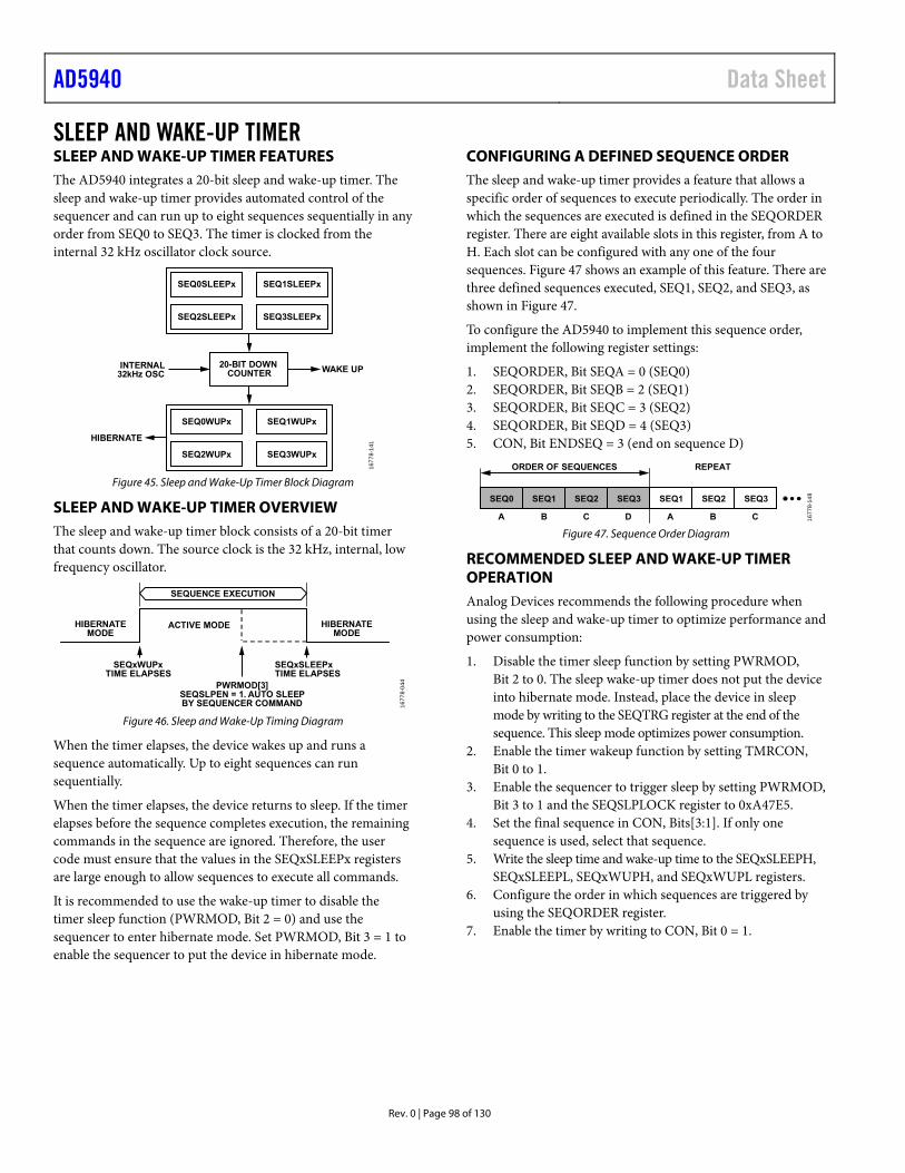
AD5940 Data Sheet
Rev. 0 | Page 98 of 130
SLEEP AND WAKE-UP TIMER SLEEP AND WAKE-UP TIMER FEATURES The AD5940 integrates a 20-bit sleep and wake-up timer. The sleep and wake-up timer provides automated control of the sequencer and can run up to eight sequences sequentially in any order from SEQ0 to SEQ3. The timer is clocked from the internal 32 kHz oscillator clock source.
20-BIT DOWNCOUNTER
INTERNAL32kHz OSC WAKE UP
SEQ1SLEEPx
SEQ2SLEEPx
SEQ0SLEEPx
SEQ3SLEEPx
SEQ1WUPx
SEQ2WUPx
SEQ0WUPx
SEQ3WUPx
HIBERNATE
1677
8-14
1
Figure 45. Sleep and Wake-Up Timer Block Diagram
SLEEP AND WAKE-UP TIMER OVERVIEW The sleep and wake-up timer block consists of a 20-bit timer that counts down. The source clock is the 32 kHz, internal, low frequency oscillator.
SEQxWUPxTIME ELAPSES
ACTIVE MODE
SEQUENCE EXECUTION
SEQxSLEEPxTIME ELAPSES
HIBERNATEMODE
PWRMOD[3]SEQSLPEN = 1. AUTO SLEEPBY SEQUENCER COMMAND
HIBERNATEMODE
1677
8-04
4
Figure 46. Sleep and Wake-Up Timing Diagram
When the timer elapses, the device wakes up and runs a sequence automatically. Up to eight sequences can run sequentially.
When the timer elapses, the device returns to sleep. If the timer elapses before the sequence completes execution, the remaining commands in the sequence are ignored. Therefore, the user code must ensure that the values in the SEQxSLEEPx registers are large enough to allow sequences to execute all commands.
It is recommended to use the wake-up timer to disable the timer sleep function (PWRMOD, Bit 2 = 0) and use the sequencer to enter hibernate mode. Set PWRMOD, Bit 3 = 1 to enable the sequencer to put the device in hibernate mode.
CONFIGURING A DEFINED SEQUENCE ORDER The sleep and wake-up timer provides a feature that allows a specific order of sequences to execute periodically. The order in which the sequences are executed is defined in the SEQORDER register. There are eight available slots in this register, from A to H. Each slot can be configured with any one of the four sequences. Figure 47 shows an example of this feature. There are three defined sequences executed, SEQ1, SEQ2, and SEQ3, as shown in Figure 47.
To configure the AD5940 to implement this sequence order, implement the following register settings:
1. SEQORDER, Bit SEQA = 0 (SEQ0) 2. SEQORDER, Bit SEQB = 2 (SEQ1) 3. SEQORDER, Bit SEQC = 3 (SEQ2) 4. SEQORDER, Bit SEQD = 4 (SEQ3) 5. CON, Bit ENDSEQ = 3 (end on sequence D)
1677
8-14
8
SEQ0 SEQ1 SEQ2 SEQ3 SEQ1 SEQ2 SEQ3
ORDER OF SEQUENCES REPEAT
A B C D A B C Figure 47. Sequence Order Diagram
RECOMMENDED SLEEP AND WAKE-UP TIMER OPERATION Analog Devices recommends the following procedure when using the sleep and wake-up timer to optimize performance and power consumption:
1. Disable the timer sleep function by setting PWRMOD, Bit 2 to 0. The sleep wake-up timer does not put the device into hibernate mode. Instead, place the device in sleep mode by writing to the SEQTRG register at the end of the sequence. This sleep mode optimizes power consumption.
2. Enable the timer wakeup function by setting TMRCON, Bit 0 to 1.
3. Enable the sequencer to trigger sleep by setting PWRMOD, Bit 3 to 1 and the SEQSLPLOCK register to 0xA47E5.
4. Set the final sequence in CON, Bits[3:1]. If only one sequence is used, select that sequence.
5. Write the sleep time and wake-up time to the SEQxSLEEPH, SEQxSLEEPL, SEQxWUPH, and SEQxWUPL registers.
6. Configure the order in which sequences are triggered by using the SEQORDER register.
7. Enable the timer by writing to CON, Bit 0 = 1.
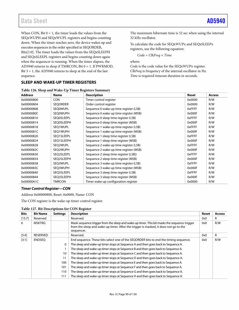
Data Sheet AD5940
Rev. 0 | Page 99 of 130
When CON, Bit 0 = 1, the timer loads the values from the SEQxWUPH and SEQxWUPL registers and begins counting down. When the timer reaches zero, the device wakes up and executes sequences in the order specified in SEQORDER, Bits[1:0]. The timer loads the values from the SEQxSLEEPH and SEQxSLEEPL registers and begins counting down again when the sequencer is running. When the timer elapses, the AD5940 returns to sleep if TMRCON, Bit 0 = 1. If PWRMOD, Bit 3 = 1, the AD5940 returns to sleep at the end of the last sequence.
The maximum hibernate time is 32 sec when using the internal 32 kHz oscillator.
To calculate the code for SEQxWUPx and SEQxSLEEPx registers, use the following equation:
Code = ClkFreq × Time
where: Code is the code value for the SEQxWUPx register. ClkFreq is frequency of the internal oscillator in Hz. Time is required timeout duration in seconds.
SLEEP AND WAKE-UP TIMER REGISTERS
Table 126. Sleep and Wake-Up Timer Registers Summary Address Name Description Reset Access 0x00000800 CON Timer control register 0x0000 R/W 0x00000804 SEQORDER Order control register 0x0000 R/W 0x00000808 SEQ0WUPL Sequence 0 wake-up time register (LSB) 0xFFFF R/W 0x0000080C SEQ0WUPH Sequence 0 wake-up time register (MSB) 0x000F R/W 0x00000810 SEQ0SLEEPL Sequence 0 sleep time register (LSB) 0xFFFF R/W 0x00000814 SEQ0SLEEPH Sequence 0 sleep time register (MSB) 0x000F R/W 0x00000818 SEQ1WUPL Sequence 1 wake-up time register (LSB) 0xFFFF R/W 0x0000081C SEQ1WUPH Sequence 1 wake-up time register (MSB) 0x000F R/W 0x00000820 SEQ1SLEEPL Sequence 1 sleep time register (LSB) 0xFFFF R/W 0x00000824 SEQ1SLEEPH Sequence 1 sleep time register (MSB) 0x000F R/W 0x00000828 SEQ2WUPL Sequence 2 wake-up time register (LSB) 0xFFFF R/W 0x0000082C SEQ2WUPH Sequence 2 wake-up time register (MSB) 0x000F R/W 0x00000830 SEQ2SLEEPL Sequence 2 sleep time register (LSB)) 0xFFFF R/W 0x00000834 SEQ2SLEEPH Sequence 2 sleep time register (MSB) 0x000F R/W 0x00000838 SEQ3WUPL Sequence 3 wake-up time register (LSB) 0xFFFF R/W 0x0000083C SEQ3WUPH Sequence 3 wake-up time register (MSB) 0x000F R/W 0x00000840 SEQ3SLEEPL Sequence 3 sleep time register (LSB) 0xFFFF R/W 0x00000844 SEQ3SLEEPH Sequence 3 sleep time register (MSB) 0x000F R/W 0x00000A1C TMRCON Timer wake-up configuration register 0x0000 R/W
Timer Control Register—CON
Address 0x00000800, Reset: 0x0000, Name: CON
The CON register is the wake-up timer control register.
Table 127. Bit Descriptions for CON Register Bits Bit Name Settings Description Reset Access [15:7] Reserved Reserved. 0x0 R 6 MSKTRG Mask sequence trigger from the sleep and wake-up timer. This bit masks the sequence trigger
from the sleep and wake-up timer. After the trigger is masked, it does not go to the sequencer.
0x0 R/W
[5:4] RESERVED Reserved. 0x0 R [3:1] ENDSEQ End sequence. These bits select one of the SEQORDER bits to end the timing sequence. 0x0 R/W 0 The sleep and wake-up timer stops at Sequence A and then goes back to Sequence A. 1 The sleep and wake-up timer stops at Sequence B and then goes back to Sequence A. 10 The sleep and wake-up timer stops at Sequence C and then goes back to Sequence A. 11 The sleep and wake-up timer stops at Sequence D and then goes back to Sequence A. 100 The sleep and wake-up timer stops at Sequence E and then goes back to Sequence A. 101 The sleep and wake-up timer stops at Sequence F and then goes back to Sequence A. 110 The sleep and wake-up timer stops at Sequence G and then goes back to Sequence A. 111 The sleep and wake-up timer stops at Sequence H and then goes back to Sequence A.
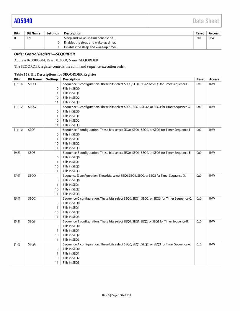
AD5940 Data Sheet
Rev. 0 | Page 100 of 130
Bits Bit Name Settings Description Reset Access 0 EN Sleep and wake-up timer enable bit. 0x0 R/W 0 Enables the sleep and wake-up timer. 1 Disables the sleep and wake-up timer.
Order Control Register—SEQORDER
Address 0x00000804, Reset: 0x0000, Name: SEQORDER
The SEQORDER register controls the command sequence execution order.
Table 128. Bit Descriptions for SEQORDER Register Bits Bit Name Settings Description Reset Access [15:14] SEQH Sequence H configuration. These bits select SEQ0, SEQ1, SEQ2, or SEQ3 for Timer Sequence H. 0x0 R/W 0 Fills in SEQ0. 1 Fills in SEQ1. 10 Fills in SEQ2. 11 Fills in SEQ3. [13:12] SEQG Sequence G configuration. These bits select SEQ0, SEQ1, SEQ2, or SEQ3 for Timer Sequence G. 0x0 R/W 0 Fills in SEQ0. 1 Fills in SEQ1. 10 Fills in SEQ2. 11 Fills in SEQ3. [11:10] SEQF Sequence F configuration. These bits select SEQ0, SEQ1, SEQ2, or SEQ3 for Timer Sequence F. 0x0 R/W 0 Fills in SEQ0. 1 Fills in SEQ1. 10 Fills in SEQ2. 11 Fills in SEQ3. [9:8] SEQE Sequence E configuration. These bits select SEQ0, SEQ1, SEQ2, or SEQ3 for Timer Sequence E. 0x0 R/W 0 Fills in SEQ0. 1 Fills in SEQ1. 10 Fills in SEQ2. 11 Fills in SEQ3. [7:6] SEQD Sequence D configuration. These bits select SEQ0, SEQ1, SEQ2, or SEQ3 for Timer Sequence D. 0x0 R/W 0 Fills in SEQ0. 1 Fills in SEQ1. 10 Fills in SEQ2. 11 Fills in SEQ3. [5:4] SEQC Sequence C configuration. These bits select SEQ0, SEQ1, SEQ2, or SEQ3 for Timer Sequence C. 0x0 R/W 0 Fills in SEQ0. 1 Fills in SEQ1. 10 Fills in SEQ2. 11 Fills in SEQ3. [3:2] SEQB Sequence B configuration. These bits select SEQ0, SEQ1, SEQ2, or SEQ3 for Timer Sequence B. 0x0 R/W 0 Fills in SEQ0. 1 Fills in SEQ1. 10 Fills in SEQ2. 11 Fills in SEQ3. [1:0] SEQA Sequence A configuration. These bits select SEQ0, SEQ1, SEQ2, or SEQ3 for Timer Sequence A. 0x0 R/W 0 Fills in SEQ0. 1 Fills in SEQ1. 10 Fills in SEQ2. 11 Fills in SEQ3.
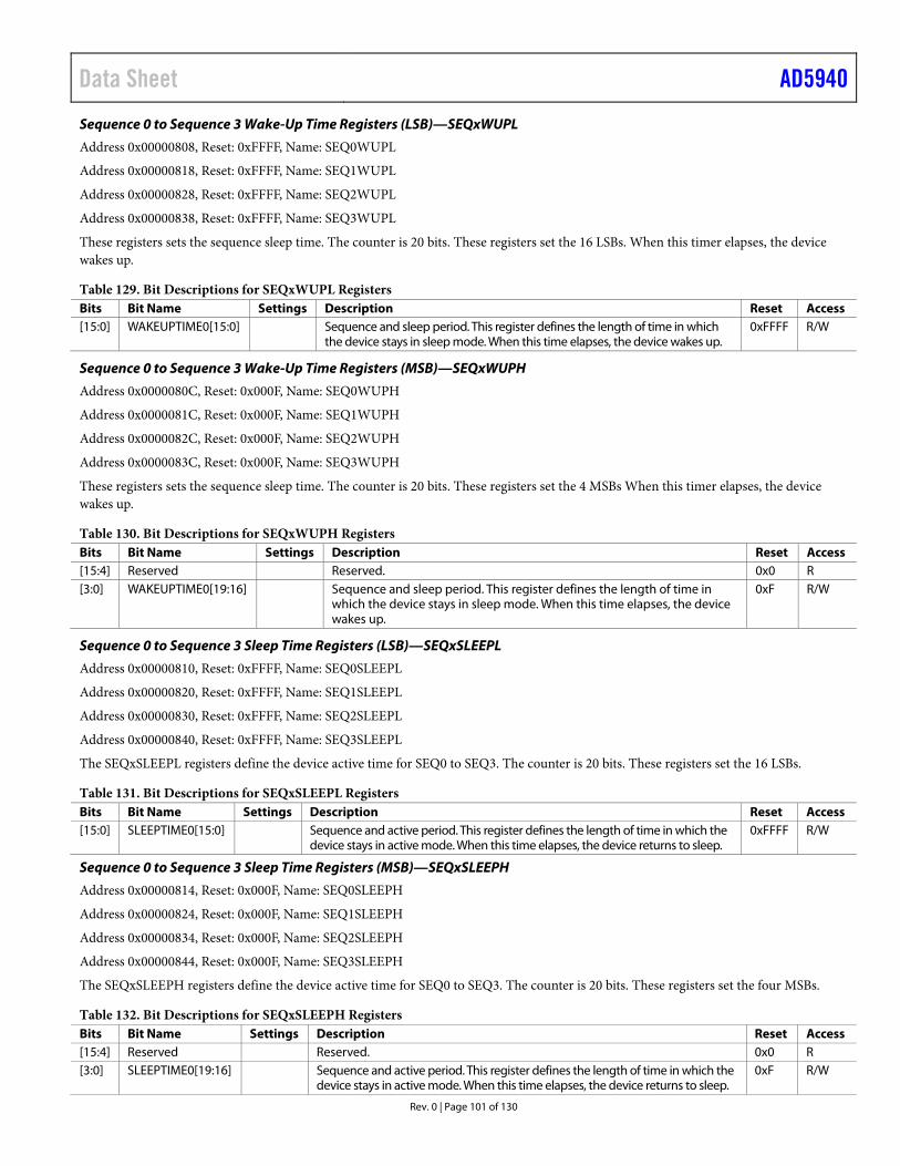
Data Sheet AD5940
Rev. 0 | Page 101 of 130
Sequence 0 to Sequence 3 Wake-Up Time Registers (LSB)—SEQxWUPL
Address 0x00000808, Reset: 0xFFFF, Name: SEQ0WUPL
Address 0x00000818, Reset: 0xFFFF, Name: SEQ1WUPL
Address 0x00000828, Reset: 0xFFFF, Name: SEQ2WUPL
Address 0x00000838, Reset: 0xFFFF, Name: SEQ3WUPL
These registers sets the sequence sleep time. The counter is 20 bits. These registers set the 16 LSBs. When this timer elapses, the device wakes up.
Table 129. Bit Descriptions for SEQxWUPL Registers Bits Bit Name Settings Description Reset Access [15:0] WAKEUPTIME0[15:0] Sequence and sleep period. This register defines the length of time in which
the device stays in sleep mode. When this time elapses, the device wakes up. 0xFFFF R/W
Sequence 0 to Sequence 3 Wake-Up Time Registers (MSB)—SEQxWUPH
Address 0x0000080C, Reset: 0x000F, Name: SEQ0WUPH
Address 0x0000081C, Reset: 0x000F, Name: SEQ1WUPH
Address 0x0000082C, Reset: 0x000F, Name: SEQ2WUPH
Address 0x0000083C, Reset: 0x000F, Name: SEQ3WUPH
These registers sets the sequence sleep time. The counter is 20 bits. These registers set the 4 MSBs When this timer elapses, the device wakes up.
Table 130. Bit Descriptions for SEQxWUPH Registers Bits Bit Name Settings Description Reset Access [15:4] Reserved Reserved. 0x0 R [3:0] WAKEUPTIME0[19:16] Sequence and sleep period. This register defines the length of time in
which the device stays in sleep mode. When this time elapses, the device wakes up.
0xF R/W
Sequence 0 to Sequence 3 Sleep Time Registers (LSB)—SEQxSLEEPL
Address 0x00000810, Reset: 0xFFFF, Name: SEQ0SLEEPL
Address 0x00000820, Reset: 0xFFFF, Name: SEQ1SLEEPL
Address 0x00000830, Reset: 0xFFFF, Name: SEQ2SLEEPL
Address 0x00000840, Reset: 0xFFFF, Name: SEQ3SLEEPL
The SEQxSLEEPL registers define the device active time for SEQ0 to SEQ3. The counter is 20 bits. These registers set the 16 LSBs.
Table 131. Bit Descriptions for SEQxSLEEPL Registers Bits Bit Name Settings Description Reset Access [15:0] SLEEPTIME0[15:0] Sequence and active period. This register defines the length of time in which the
device stays in active mode. When this time elapses, the device returns to sleep. 0xFFFF R/W
Sequence 0 to Sequence 3 Sleep Time Registers (MSB)—SEQxSLEEPH
Address 0x00000814, Reset: 0x000F, Name: SEQ0SLEEPH
Address 0x00000824, Reset: 0x000F, Name: SEQ1SLEEPH
Address 0x00000834, Reset: 0x000F, Name: SEQ2SLEEPH
Address 0x00000844, Reset: 0x000F, Name: SEQ3SLEEPH
The SEQxSLEEPH registers define the device active time for SEQ0 to SEQ3. The counter is 20 bits. These registers set the four MSBs.
Table 132. Bit Descriptions for SEQxSLEEPH Registers Bits Bit Name Settings Description Reset Access [15:4] Reserved Reserved. 0x0 R [3:0] SLEEPTIME0[19:16] Sequence and active period. This register defines the length of time in which the
device stays in active mode. When this time elapses, the device returns to sleep. 0xF R/W
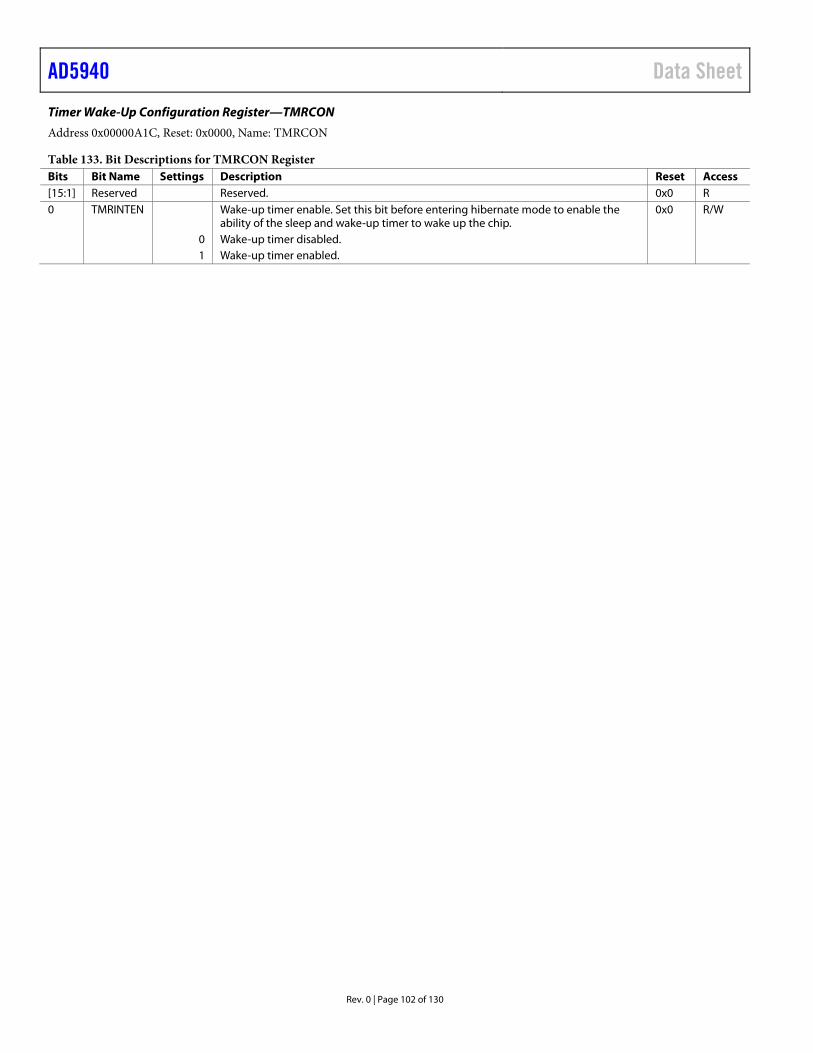
AD5940 Data Sheet
Rev. 0 | Page 102 of 130
Timer Wake-Up Configuration Register—TMRCON
Address 0x00000A1C, Reset: 0x0000, Name: TMRCON
Table 133. Bit Descriptions for TMRCON Register Bits Bit Name Settings Description Reset Access [15:1] Reserved Reserved. 0x0 R 0 TMRINTEN Wake-up timer enable. Set this bit before entering hibernate mode to enable the
ability of the sleep and wake-up timer to wake up the chip. 0x0 R/W
0 Wake-up timer disabled. 1 Wake-up timer enabled.
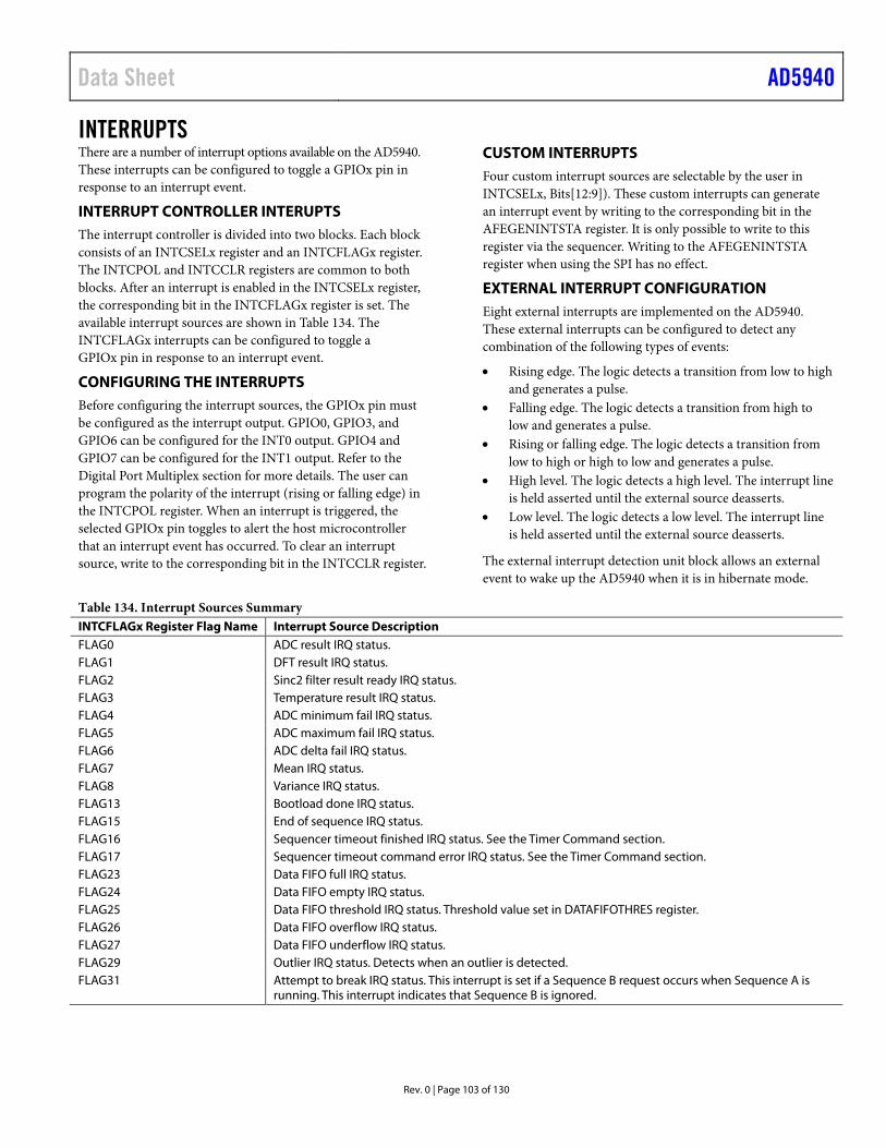
Data Sheet AD5940
Rev. 0 | Page 103 of 130
INTERRUPTS There are a number of interrupt options available on the AD5940. These interrupts can be configured to toggle a GPIOx pin in response to an interrupt event.
INTERRUPT CONTROLLER INTERUPTS The interrupt controller is divided into two blocks. Each block consists of an INTCSELx register and an INTCFLAGx register. The INTCPOL and INTCCLR registers are common to both blocks. After an interrupt is enabled in the INTCSELx register, the corresponding bit in the INTCFLAGx register is set. The available interrupt sources are shown in Table 134. The INTCFLAGx interrupts can be configured to toggle a GPIOx pin in response to an interrupt event.
CONFIGURING THE INTERRUPTS Before configuring the interrupt sources, the GPIOx pin must be configured as the interrupt output. GPIO0, GPIO3, and GPIO6 can be configured for the INT0 output. GPIO4 and GPIO7 can be configured for the INT1 output. Refer to the Digital Port Multiplex section for more details. The user can program the polarity of the interrupt (rising or falling edge) in the INTCPOL register. When an interrupt is triggered, the selected GPIOx pin toggles to alert the host microcontroller that an interrupt event has occurred. To clear an interrupt source, write to the corresponding bit in the INTCCLR register.
CUSTOM INTERRUPTS Four custom interrupt sources are selectable by the user in INTCSELx, Bits[12:9]). These custom interrupts can generate an interrupt event by writing to the corresponding bit in the AFEGENINTSTA register. It is only possible to write to this register via the sequencer. Writing to the AFEGENINTSTA register when using the SPI has no effect.
EXTERNAL INTERRUPT CONFIGURATION Eight external interrupts are implemented on the AD5940. These external interrupts can be configured to detect any combination of the following types of events:
• Rising edge. The logic detects a transition from low to high and generates a pulse.
• Falling edge. The logic detects a transition from high to low and generates a pulse.
• Rising or falling edge. The logic detects a transition from low to high or high to low and generates a pulse.
• High level. The logic detects a high level. The interrupt line is held asserted until the external source deasserts.
• Low level. The logic detects a low level. The interrupt line is held asserted until the external source deasserts.
The external interrupt detection unit block allows an external event to wake up the AD5940 when it is in hibernate mode.
Table 134. Interrupt Sources Summary INTCFLAGx Register Flag Name Interrupt Source Description FLAG0 ADC result IRQ status. FLAG1 DFT result IRQ status. FLAG2 Sinc2 filter result ready IRQ status. FLAG3 Temperature result IRQ status. FLAG4 ADC minimum fail IRQ status. FLAG5 ADC maximum fail IRQ status. FLAG6 ADC delta fail IRQ status. FLAG7 Mean IRQ status. FLAG8 Variance IRQ status. FLAG13 Bootload done IRQ status. FLAG15 End of sequence IRQ status. FLAG16 Sequencer timeout finished IRQ status. See the Timer Command section. FLAG17 Sequencer timeout command error IRQ status. See the Timer Command section. FLAG23 Data FIFO full IRQ status. FLAG24 Data FIFO empty IRQ status. FLAG25 Data FIFO threshold IRQ status. Threshold value set in DATAFIFOTHRES register. FLAG26 Data FIFO overflow IRQ status. FLAG27 Data FIFO underflow IRQ status. FLAG29 Outlier IRQ status. Detects when an outlier is detected. FLAG31 Attempt to break IRQ status. This interrupt is set if a Sequence B request occurs when Sequence A is
running. This interrupt indicates that Sequence B is ignored.
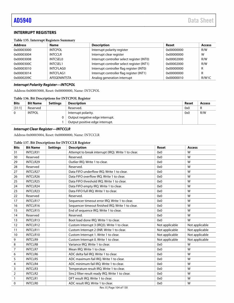
AD5940 Data Sheet
Rev. 0 | Page 104 of 130
INTERRUPT REGISTERS
Table 135. Interrupt Registers Summary Address Name Description Reset Access 0x00003000 INTCPOL Interrupt polarity register 0x00000000 R/W 0x00003004 INTCCLR Interrupt clear register 0x00000000 W 0x00003008 INTCSEL0 Interrupt controller select register (INT0) 0x00002000 R/W 0x0000300C INTCSEL1 Interrupt controller select register (INT1) 0x00002000 R/W 0x00003010 INTCFLAG0 Interrupt controller flag register (INT0) 0x00000000 R 0x00003014 INTCFLAG1 Interrupt controller flag register (INT1) 0x00000000 R 0x0000209C AFEGENINTSTA Analog generation interrupt 0x00000010 R/W1C
Interrupt Polarity Register—INTCPOL
Address 0x00003000, Reset: 0x00000000, Name: INTCPOL
Table 136. Bit Descriptions for INTCPOL Register Bits Bit Name Settings Description Reset Access [31:1] Reserved Reserved. 0x0 R 0 INTPOL Interrupt polarity. 0x0 R/W 0 Output negative edge interrupt. 1 Output positive edge interrupt.
Interrupt Clear Register—INTCCLR
Address 0x00003004, Reset: 0x00000000, Name: INTCCLR
Table 137. Bit Descriptions for INTCCLR Register Bits Bit Name Settings Description Reset Access 31 INTCLR31 Attempt to break interrupt (IRQ). Write 1 to clear. 0x0 W 30 Reserved Reserved. 0x0 W 29 INTCLR29 Outlier IRQ. Write 1 to clear. 0x0 W 28 Reserved Reserved. 0x0 W 27 INTCLR27 Data FIFO underflow IRQ. Write 1 to clear. 0x0 W 26 INTCLR26 Data FIFO overflow IRQ. Write 1 to clear. 0x0 W 25 INTCLR25 Data FIFO threshold IRQ. Write 1 to clear. 0x0 W 24 INTCLR24 Data FIFO empty IRQ. Write 1 to clear. 0x0 W 23 INTCLR23 Data FIFO full IRQ. Write 1 to clear. 0x0 W 22 Reserved Reserved. 0x0 W 17 INTCLR17 Sequencer timeout error IRQ. Write 1 to clear. 0x0 W 16 INTCLR16 Sequencer timeout finished IRQ. Write 1 to clear. 0x0 W 15 INTCLR15 End of sequence IRQ. Write 1 to clear. 0x0 W 14 Reserved Reserved. 0x0 W 13 INTCLR13 Boot load done IRQ. Write 1 to clear. 0x0 W 12 INTCLR12 Custom Interrupt 3 (IRQ3). Write 1 to clear. Not applicable Not applicable 11 INTCLR11 Custom Interrupt 2 (INR. Write 1 to clear. Not applicable Not applicable 10 INTCLR10 Custom Interrupt 1. Write 1 to clear. Not applicable Not applicable 9 INTCLR9 Custom Interrupt 0. Write 1 to clear. Not applicable Not applicable 8 INTCLR8 Variance IRQ. Write 1 to clear. 0x0 W 7 INTCLR7 Mean IRQ. Write 1 to clear. 0x0 W 6 INTCLR6 ADC delta fail IRQ. Write 1 to clear. 0x0 W 5 INTCLR5 ADC maximum fail IRQ. Write 1 to clear. 0x0 W 4 INTCLR4 ADC minimum fail IRQ. Write 1 to clear. 0x0 W 3 INTCLR3 Temperature result IRQ. Write 1 to clear. 0x0 W 2 INTCLR2 Sinc2 filter result ready IRQ. Write 1 to clear. 0x0 W 1 INTCLR1 DFT result IRQ. Write 1 to clear. 0x0 W 0 INTCLR0 ADC result IRQ. Write 1 to clear. 0x0 W
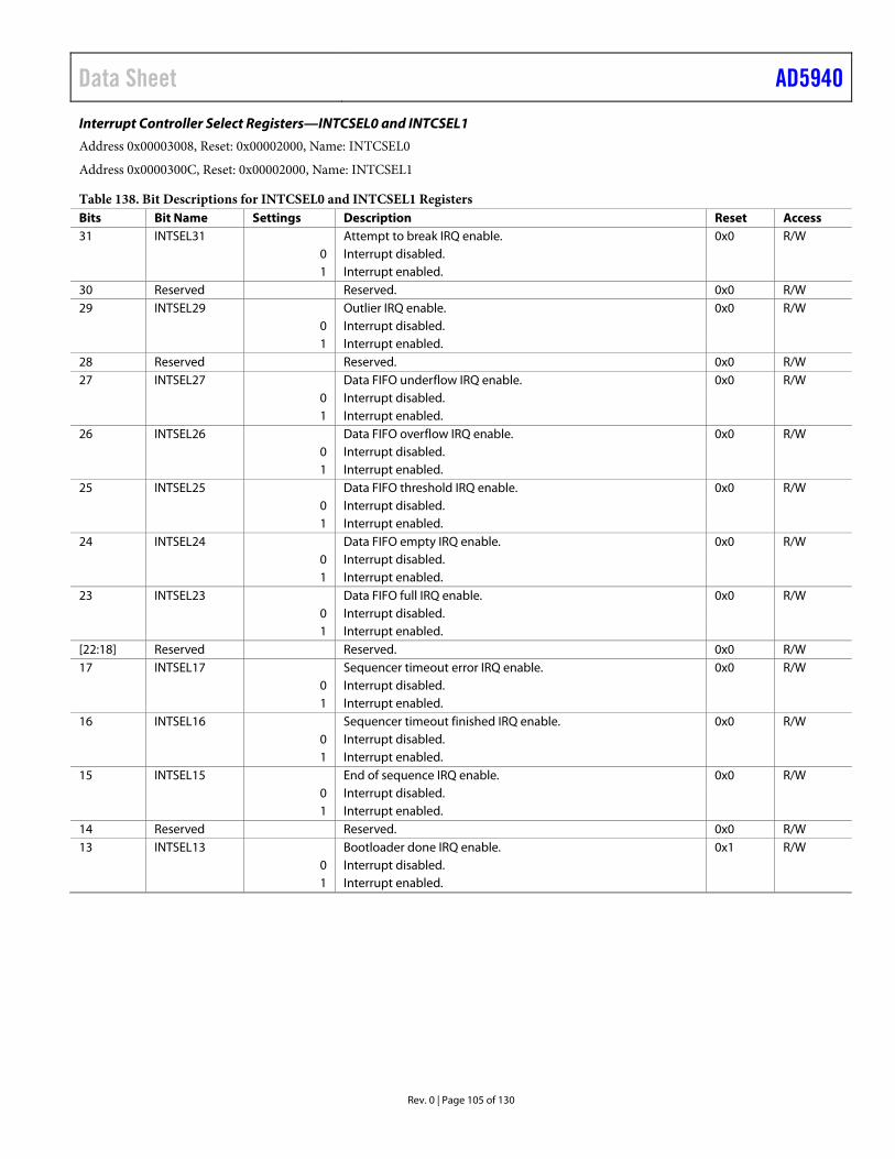
Data Sheet AD5940
Rev. 0 | Page 105 of 130
Interrupt Controller Select Registers—INTCSEL0 and INTCSEL1
Address 0x00003008, Reset: 0x00002000, Name: INTCSEL0
Address 0x0000300C, Reset: 0x00002000, Name: INTCSEL1
Table 138. Bit Descriptions for INTCSEL0 and INTCSEL1 Registers Bits Bit Name Settings Description Reset Access 31 INTSEL31 Attempt to break IRQ enable. 0x0 R/W 0 Interrupt disabled. 1 Interrupt enabled. 30 Reserved Reserved. 0x0 R/W 29 INTSEL29 Outlier IRQ enable. 0x0 R/W 0 Interrupt disabled. 1 Interrupt enabled. 28 Reserved Reserved. 0x0 R/W 27 INTSEL27 Data FIFO underflow IRQ enable. 0x0 R/W 0 Interrupt disabled. 1 Interrupt enabled. 26 INTSEL26 Data FIFO overflow IRQ enable. 0x0 R/W 0 Interrupt disabled. 1 Interrupt enabled. 25 INTSEL25 Data FIFO threshold IRQ enable. 0x0 R/W 0 Interrupt disabled. 1 Interrupt enabled. 24 INTSEL24 Data FIFO empty IRQ enable. 0x0 R/W 0 Interrupt disabled. 1 Interrupt enabled. 23 INTSEL23 Data FIFO full IRQ enable. 0x0 R/W 0 Interrupt disabled. 1 Interrupt enabled. [22:18] Reserved Reserved. 0x0 R/W 17 INTSEL17 Sequencer timeout error IRQ enable. 0x0 R/W 0 Interrupt disabled. 1 Interrupt enabled. 16 INTSEL16 Sequencer timeout finished IRQ enable. 0x0 R/W 0 Interrupt disabled. 1 Interrupt enabled. 15 INTSEL15 End of sequence IRQ enable. 0x0 R/W 0 Interrupt disabled. 1 Interrupt enabled. 14 Reserved Reserved. 0x0 R/W 13 INTSEL13 Bootloader done IRQ enable. 0x1 R/W 0 Interrupt disabled. 1 Interrupt enabled.
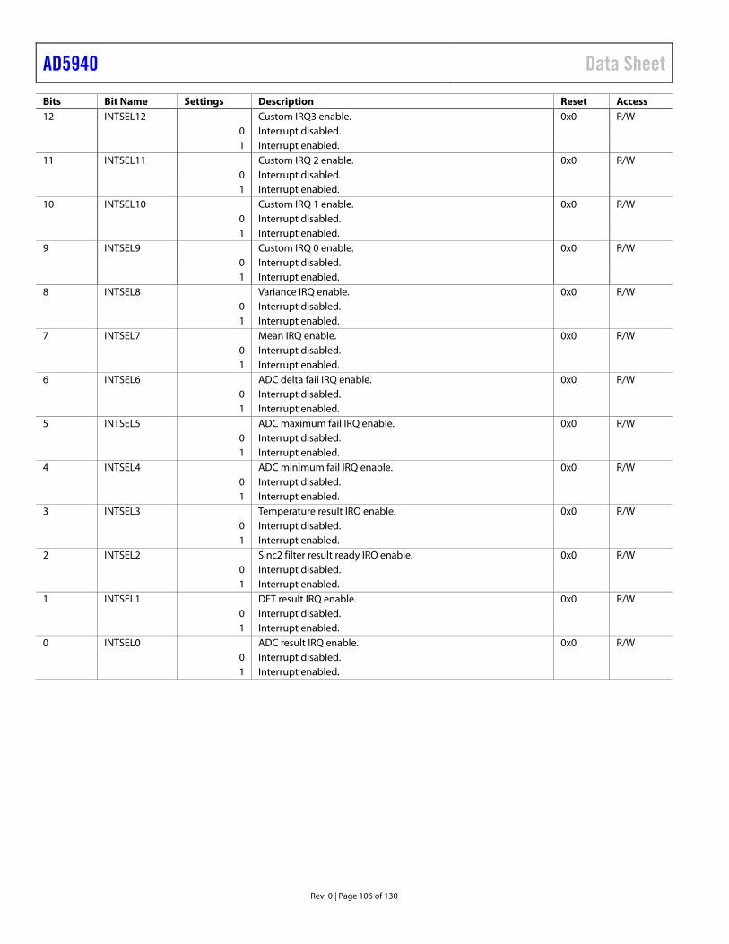
AD5940 Data Sheet
Rev. 0 | Page 106 of 130
Bits Bit Name Settings Description Reset Access 12 INTSEL12 Custom IRQ3 enable. 0x0 R/W 0 Interrupt disabled. 1 Interrupt enabled. 11 INTSEL11 Custom IRQ 2 enable. 0x0 R/W 0 Interrupt disabled. 1 Interrupt enabled. 10 INTSEL10 Custom IRQ 1 enable. 0x0 R/W 0 Interrupt disabled. 1 Interrupt enabled. 9 INTSEL9 Custom IRQ 0 enable. 0x0 R/W 0 Interrupt disabled. 1 Interrupt enabled. 8 INTSEL8 Variance IRQ enable. 0x0 R/W 0 Interrupt disabled. 1 Interrupt enabled. 7 INTSEL7 Mean IRQ enable. 0x0 R/W 0 Interrupt disabled. 1 Interrupt enabled. 6 INTSEL6 ADC delta fail IRQ enable. 0x0 R/W 0 Interrupt disabled. 1 Interrupt enabled. 5 INTSEL5 ADC maximum fail IRQ enable. 0x0 R/W 0 Interrupt disabled. 1 Interrupt enabled. 4 INTSEL4 ADC minimum fail IRQ enable. 0x0 R/W 0 Interrupt disabled. 1 Interrupt enabled. 3 INTSEL3 Temperature result IRQ enable. 0x0 R/W 0 Interrupt disabled. 1 Interrupt enabled. 2 INTSEL2 Sinc2 filter result ready IRQ enable. 0x0 R/W 0 Interrupt disabled. 1 Interrupt enabled. 1 INTSEL1 DFT result IRQ enable. 0x0 R/W 0 Interrupt disabled. 1 Interrupt enabled. 0 INTSEL0 ADC result IRQ enable. 0x0 R/W 0 Interrupt disabled. 1 Interrupt enabled.
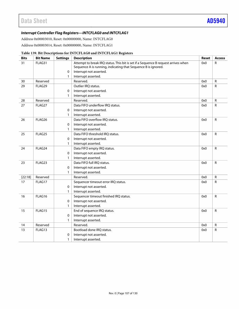
Data Sheet AD5940
Rev. 0 | Page 107 of 130
Interrupt Controller Flag Registers—INTCFLAG0 and INTCFLAG1
Address 0x00003010, Reset: 0x00000000, Name: INTCFLAG0
Address 0x00003014, Reset: 0x00000000, Name: INTCFLAG1
Table 139. Bit Descriptions for INTCFLAG0 and INTCFLAG1 Registers Bits Bit Name Settings Description Reset Access 31 FLAG31 Attempt to break IRQ status. This bit is set if a Sequence B request arrives when
Sequence A is running, indicating that Sequence B is ignored. 0x0 R
0 Interrupt not asserted. 1 Interrupt asserted. 30 Reserved Reserved. 0x0 R 29 FLAG29 Outlier IRQ status. 0x0 R 0 Interrupt not asserted. 1 Interrupt asserted. 28 Reserved Reserved. 0x0 R 27 FLAG27 Data FIFO underflow IRQ status. 0x0 R 0 Interrupt not asserted. 1 Interrupt asserted. 26 FLAG26 Data FIFO overflow IRQ status. 0x0 R 0 Interrupt not asserted. 1 Interrupt asserted. 25 FLAG25 Data FIFO threshold IRQ status. 0x0 R 0 Interrupt not asserted. 1 Interrupt asserted. 24 FLAG24 Data FIFO empty IRQ status. 0x0 R 0 Interrupt not asserted. 1 Interrupt asserted. 23 FLAG23 Data FIFO full IRQ status. 0x0 R 0 Interrupt not asserted. 1 Interrupt asserted. [22:18] Reserved Reserved. 0x0 R 17 FLAG17 Sequencer timeout error IRQ status. 0x0 R 0 Interrupt not asserted. 1 Interrupt asserted. 16 FLAG16 Sequencer timeout finished IRQ status. 0x0 R 0 Interrupt not asserted. 1 Interrupt asserted. 15 FLAG15 End of sequence IRQ status. 0x0 R 0 Interrupt not asserted. 1 Interrupt asserted. 14 Reserved Reserved. 0x0 R 13 FLAG13 Bootload done IRQ status. 0x0 R 0 Interrupt not asserted. 1 Interrupt asserted.
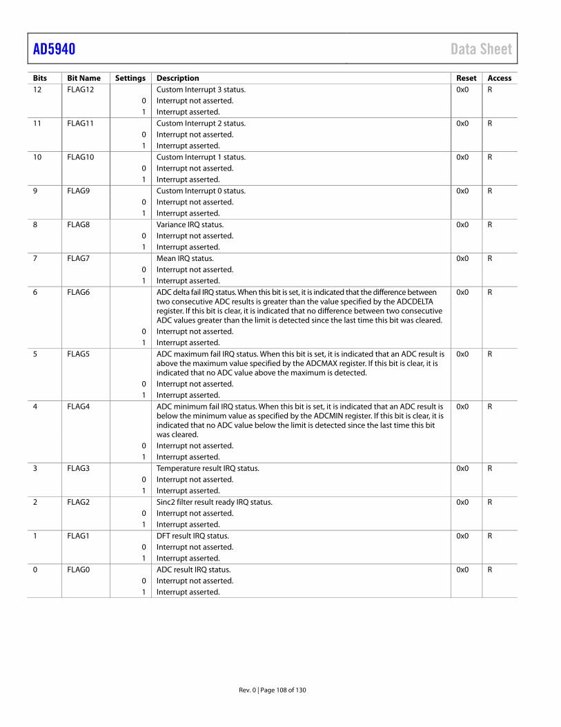
AD5940 Data Sheet
Rev. 0 | Page 108 of 130
Bits Bit Name Settings Description Reset Access 12 FLAG12 Custom Interrupt 3 status. 0x0 R 0 Interrupt not asserted. 1 Interrupt asserted. 11 FLAG11 Custom Interrupt 2 status. 0x0 R 0 Interrupt not asserted. 1 Interrupt asserted. 10 FLAG10 Custom Interrupt 1 status. 0x0 R 0 Interrupt not asserted. 1 Interrupt asserted. 9 FLAG9 Custom Interrupt 0 status. 0x0 R 0 Interrupt not asserted. 1 Interrupt asserted. 8 FLAG8 Variance IRQ status. 0x0 R 0 Interrupt not asserted. 1 Interrupt asserted. 7 FLAG7 Mean IRQ status. 0x0 R 0 Interrupt not asserted. 1 Interrupt asserted. 6 FLAG6 ADC delta fail IRQ status. When this bit is set, it is indicated that the difference between
two consecutive ADC results is greater than the value specified by the ADCDELTA register. If this bit is clear, it is indicated that no difference between two consecutive ADC values greater than the limit is detected since the last time this bit was cleared.
0x0 R
0 Interrupt not asserted. 1 Interrupt asserted. 5 FLAG5 ADC maximum fail IRQ status. When this bit is set, it is indicated that an ADC result is
above the maximum value specified by the ADCMAX register. If this bit is clear, it is indicated that no ADC value above the maximum is detected.
0x0 R
0 Interrupt not asserted. 1 Interrupt asserted. 4 FLAG4 ADC minimum fail IRQ status. When this bit is set, it is indicated that an ADC result is
below the minimum value as specified by the ADCMIN register. If this bit is clear, it is indicated that no ADC value below the limit is detected since the last time this bit was cleared.
0x0 R
0 Interrupt not asserted. 1 Interrupt asserted. 3 FLAG3 Temperature result IRQ status. 0x0 R 0 Interrupt not asserted. 1 Interrupt asserted. 2 FLAG2 Sinc2 filter result ready IRQ status. 0x0 R 0 Interrupt not asserted. 1 Interrupt asserted. 1 FLAG1 DFT result IRQ status. 0x0 R 0 Interrupt not asserted. 1 Interrupt asserted. 0 FLAG0 ADC result IRQ status. 0x0 R 0 Interrupt not asserted. 1 Interrupt asserted.
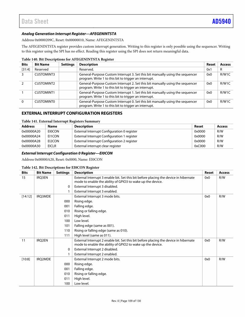
Data Sheet AD5940
Rev. 0 | Page 109 of 130
Analog Generation Interrupt Register—AFEGENINTSTA
Address 0x0000209C, Reset: 0x00000010, Name: AFEGENINTSTA
The AFEGENINTSTA register provides custom interrupt generation. Writing to this register is only possible using the sequencer. Writing to this register using the SPI has no effect. Reading this register using the SPI does not return meaningful data.
Table 140. Bit Descriptions for AFEGENINTSTA Register Bits Bit Name Settings Description Reset Access [31:4] Reserved Reserved. 0x1 R 3 CUSTOMINT3 General-Purpose Custom Interrupt 3. Set this bit manually using the sequencer
program. Write 1 to this bit to trigger an interrupt. 0x0 R/W1C
2 CUSTOMINT2 General-Purpose Custom Interrupt 2. Set this bit manually using the sequencer program. Write 1 to this bit to trigger an interrupt.
0x0 R/W1C
1 CUSTOMINT1 General-Purpose Custom Interrupt 1. Set this bit manually using the sequencer program. Write 1 to this bit to trigger an interrupt.
0x0 R/W1C
0 CUSTOMINT0 General-Purpose Custom Interrupt 0. Set this bit manually using the sequencer program. Write 1 to this bit to trigger an interrupt.
0x0 R/W1C
EXTERNAL INTERRUPT CONFIGURATION REGISTERS
Table 141. External Interrupt Registers Summary Address Name Description Reset Access 0x00000A20 EI0CON External Interrupt Configuration 0 register 0x0000 R/W 0x00000A24 EI1CON External Interrupt Configuration 1 register 0x0000 R/W 0x00000A28 EI2CON External Interrupt Configuration 2 register 0x0000 R/W 0x00000A30 EICLR External interrupt clear register 0xC000 R/W
External Interrupt Configuration 0 Register—EI0CON
Address 0x00000A20, Reset: 0x0000, Name: EI0CON
Table 142. Bit Descriptions for EI0CON Register Bits Bit Name Settings Description Reset Access 15 IRQ3EN External Interrupt 3 enable bit. Set this bit before placing the device in hibernate
mode to enable the ability of GPIO3 to wake up the device. 0x0 R/W
0 External Interrupt 3 disabled. 1 External Interrupt 3 enabled. [14:12] IRQ3MDE External Interrupt 3 mode bits. 0x0 R/W 000 Rising edge. 001 Falling edge. 010 Rising or falling edge. 011 High level. 100 Low level. 101 Falling edge (same as 001). 110 Rising or falling edge (same as 010). 111 High level (same as 011). 11 IRQ2EN External Interrupt 2 enable bit. Set this bit before placing the device in hibernate
mode to enable the ability of GPIO2 to wake up the device. 0x0 R/W
0 External Interrupt 2 disabled. 1 External Interrupt 2 enabled. [10:8] IRQ2MDE External Interrupt 2 mode bits. 0x0 R/W 000 Rising edge. 001 Falling edge. 010 Rising or falling edge. 011 High level. 100 Low level.
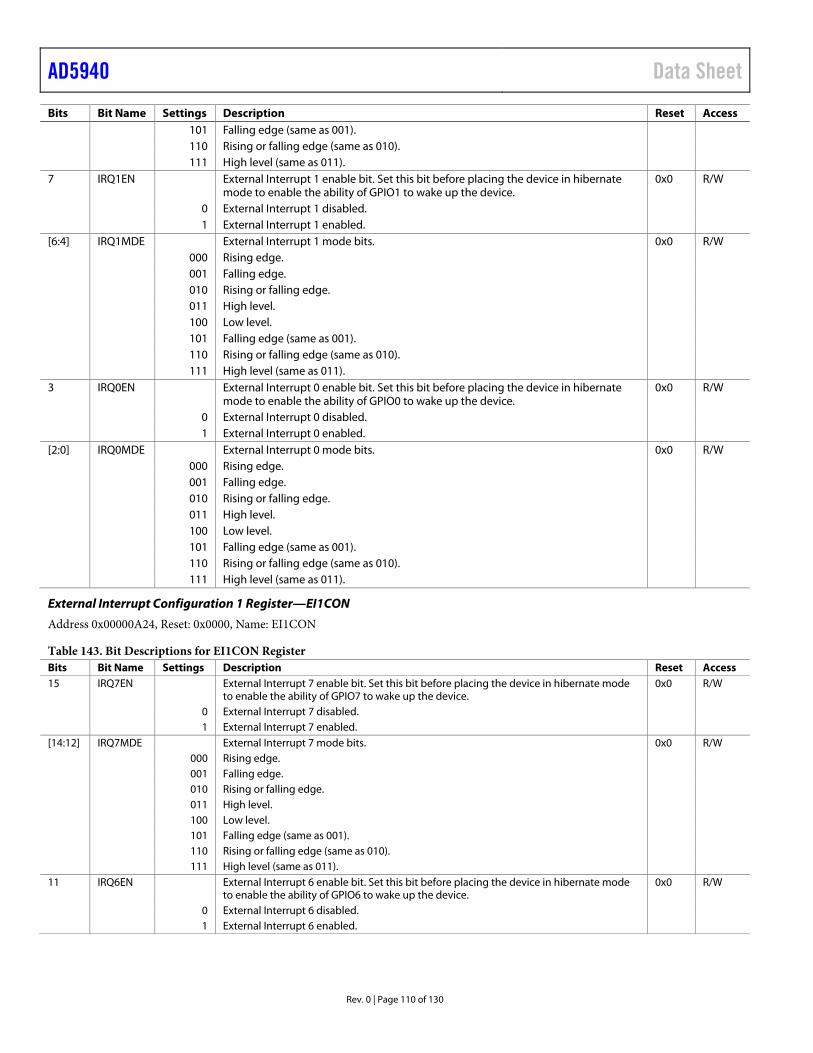
AD5940 Data Sheet
Rev. 0 | Page 110 of 130
Bits Bit Name Settings Description Reset Access 101 Falling edge (same as 001). 110 Rising or falling edge (same as 010). 111 High level (same as 011). 7 IRQ1EN External Interrupt 1 enable bit. Set this bit before placing the device in hibernate
mode to enable the ability of GPIO1 to wake up the device. 0x0 R/W
0 External Interrupt 1 disabled. 1 External Interrupt 1 enabled. [6:4] IRQ1MDE External Interrupt 1 mode bits. 0x0 R/W 000 Rising edge. 001 Falling edge. 010 Rising or falling edge. 011 High level. 100 Low level. 101 Falling edge (same as 001). 110 Rising or falling edge (same as 010). 111 High level (same as 011). 3 IRQ0EN External Interrupt 0 enable bit. Set this bit before placing the device in hibernate
mode to enable the ability of GPIO0 to wake up the device. 0x0 R/W
0 External Interrupt 0 disabled. 1 External Interrupt 0 enabled. [2:0] IRQ0MDE External Interrupt 0 mode bits. 0x0 R/W 000 Rising edge. 001 Falling edge. 010 Rising or falling edge. 011 High level. 100 Low level. 101 Falling edge (same as 001). 110 Rising or falling edge (same as 010). 111 High level (same as 011).
External Interrupt Configuration 1 Register—EI1CON
Address 0x00000A24, Reset: 0x0000, Name: EI1CON
Table 143. Bit Descriptions for EI1CON Register Bits Bit Name Settings Description Reset Access 15 IRQ7EN External Interrupt 7 enable bit. Set this bit before placing the device in hibernate mode
to enable the ability of GPIO7 to wake up the device. 0x0 R/W
0 External Interrupt 7 disabled. 1 External Interrupt 7 enabled. [14:12] IRQ7MDE External Interrupt 7 mode bits. 0x0 R/W 000 Rising edge. 001 Falling edge. 010 Rising or falling edge. 011 High level. 100 Low level. 101 Falling edge (same as 001). 110 Rising or falling edge (same as 010). 111 High level (same as 011). 11 IRQ6EN External Interrupt 6 enable bit. Set this bit before placing the device in hibernate mode
to enable the ability of GPIO6 to wake up the device. 0x0 R/W
0 External Interrupt 6 disabled. 1 External Interrupt 6 enabled.
Data Sheet AD5940
Rev. 0 | Page 111 of 130
Bits Bit Name Settings Description Reset Access [10:8] IRQ6MDE External Interrupt 6 mode bits. 0x0 R/W 000 Rising edge. 001 Falling edge. 010 Rising or falling edge. 011 High level. 100 Low level. 101 Falling edge (same as 001). 110 Rising or falling edge (same as 010). 111 High level (same as 011). 7 IRQ5EN External Interrupt 5 enable bit. Set this bit before placing the device in hibernate mode
to enable the ability of GPIO5 to wake up the device. 0x0 R/W
0 External Interrupt 5 disabled. 1 External Interrupt 5 enabled. [6:4] IRQ5MDE External Interrupt 5 mode bits. 0x0 R/W 000 Rising edge. 001 Falling edge. 010 Rising or falling edge. 011 High level. 100 Low level. 101 Falling edge (same as 001). 110 Rising or falling edge (same as 010). 111 High level (same as 011). 3 IRQ4EN External Interrupt 4 enable bit. Set this bit before placing the device in hibernate mode
to enable the ability of GPIO4 to wake up the device. 0x0 R/W
0 External Interrupt 4 disabled. 1 External Interrupt 4 enabled. [2:0] IRQ4MDE External Interrupt 4 mode bits. 0x0 R/W 000 Rising edge. 001 Falling edge. 010 Rising or falling edge. 011 High level. 100 Low level. 101 Falling edge (same as 001). 110 Rising or falling edge (same as 010). 111 High level (same as 011).
External Interrupt Configuration 2 Register—EI2CON
Address 0x00000A28, Reset: 0x0000, Name: EI2CON
Table 144. Bit Descriptions for EI2CON Register Bits Bit Name Settings Description Reset Access [15:4] Reserved Reserved. 0x0 R 3 BUSINTEN Bus interrupt detection enable bit. Set this bit before placing the device in hibernate
mode to enable the ability of the SPI to wake up the device. 0x0 R/W
0 Bus interrupt wake-up disabled. 1 Bus interrupt wake-up enabled. [2:0] BUSINTMDE Bus interrupt detection mode bits. 0x0 R/W 000 Rising edge. 001 Falling edge. 010 Rising or falling edge. 011 High level. 100 Low level. 101 Falling edge (same as 001). 110 Rising or falling edge (same as 010). 111 High level (same as 011).
AD5940 Data Sheet
Rev. 0 | Page 112 of 130
External Interrupt Clear Register—EICLR
Address 0x00000A30, Reset: 0xC000, Name: EICLR
Table 145. Bit Descriptions for EICLR Register Bits Bit Name Settings Description Reset Access 15 AUTCLRBUSEN Enable autoclear of bus interrupt. Set this bit to 1 to enable autoclear. 0x1 R/W 14 AUTCLRIRQEN Enable autoclear of External Interrupt 0 to External Interrupt 7. Set this bit to 1
to enable autoclear. 0x1 R/W
[13:9] Reserved Reserved. 0x0 R 8 BUSINT Bus interrupt. Set this bit to 1 to clear an internal interrupt flag. This bit is cleared
automatically by the hardware. 0x0 R/W
7 IRQ7 External Interrupt 7. Set this bit to 1 to clear an internal interrupt flag. This bit is cleared automatically by the hardware.
0x0 R/W
6 IRQ6 External Interrupt 6. Set this bit to 1 to clear an internal interrupt flag. This bit is cleared automatically by the hardware.
0x0 R/W
5 IRQ5 External Interrupt 5. Set this bit to 1 to clear an internal interrupt flag. This bit is cleared automatically by the hardware.
0x0 R/W
4 IRQ4 External Interrupt 4. Set this bit to 1 to clear an internal interrupt flag. This bit is cleared automatically by the hardware.
0x0 R/W
3 IRQ3 External Interrupt 3. Set this bit to 1 to clear an internal interrupt flag. This bit is cleared automatically by the hardware.
0x0 R/W
2 IRQ2 External Interrupt 2. Set this bit to 1 to clear an internal interrupt flag. This bit is cleared automatically by the hardware.
0x0 R/W
1 IRQ1 External Interrupt 1. Set this bit to 1 to clear an internal interrupt flag. This bit is cleared automatically by the hardware.
0x0 R/W
0 IRQ0 External Interrupt 0. Set this bit to 1 to clear an internal interrupt flag. This bit is cleared automatically by the hardware.
0x0 R/W
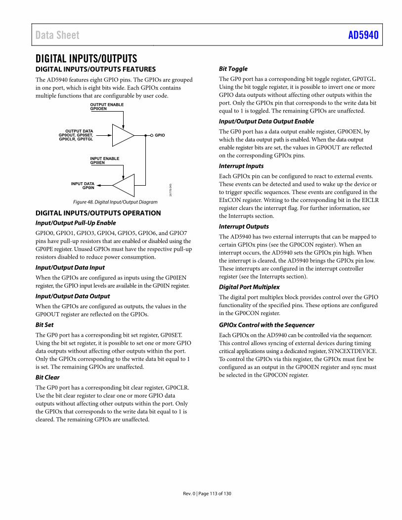
Data Sheet AD5940
Rev. 0 | Page 113 of 130
DIGITAL INPUTS/OUTPUTS DIGITAL INPUTS/OUTPUTS FEATURES The AD5940 features eight GPIO pins. The GPIOs are grouped in one port, which is eight bits wide. Each GPIOx contains multiple functions that are configurable by user code.
OUTPUT ENABLEGP0OEN
GPIO
INPUT ENABLEGP0IEN
INPUT DATAGP0IN
OUTPUT DATAGP0OUT, GP0SET,GP0CLR, GP0TGL
1677
8-04
5
Figure 48. Digital Input/Output Diagram
DIGITAL INPUTS/OUTPUTS OPERATION Input/Output Pull-Up Enable
GPIO0, GPIO1, GPIO3, GPIO4, GPIO5, GPIO6, and GPIO7 pins have pull-up resistors that are enabled or disabled using the GP0PE register. Unused GPIOs must have the respective pull-up resistors disabled to reduce power consumption.
Input/Output Data Input
When the GPIOs are configured as inputs using the GP0IEN register, the GPIO input levels are available in the GP0IN register.
Input/Output Data Output
When the GPIOs are configured as outputs, the values in the GP0OUT register are reflected on the GPIOs.
Bit Set
The GP0 port has a corresponding bit set register, GP0SET. Using the bit set register, it is possible to set one or more GPIO data outputs without affecting other outputs within the port. Only the GPIOx corresponding to the write data bit equal to 1 is set. The remaining GPIOs are unaffected.
Bit Clear
The GP0 port has a corresponding bit clear register, GP0CLR. Use the bit clear register to clear one or more GPIO data outputs without affecting other outputs within the port. Only the GPIOx that corresponds to the write data bit equal to 1 is cleared. The remaining GPIOs are unaffected.
Bit Toggle
The GP0 port has a corresponding bit toggle register, GP0TGL. Using the bit toggle register, it is possible to invert one or more GPIO data outputs without affecting other outputs within the port. Only the GPIOx pin that corresponds to the write data bit equal to 1 is toggled. The remaining GPIOs are unaffected.
Input/Output Data Output Enable
The GP0 port has a data output enable register, GP0OEN, by which the data output path is enabled. When the data output enable register bits are set, the values in GP0OUT are reflected on the corresponding GPIOx pins.
Interrupt Inputs
Each GPIOx pin can be configured to react to external events. These events can be detected and used to wake up the device or to trigger specific sequences. These events are configured in the EIxCON register. Writing to the corresponding bit in the EICLR register clears the interrupt flag. For further information, see the Interrupts section.
Interrupt Outputs
The AD5940 has two external interrupts that can be mapped to certain GPIOx pins (see the GP0CON register). When an interrupt occurs, the AD5940 sets the GPIOx pin high. When the interrupt is cleared, the AD5940 brings the GPIOx pin low. These interrupts are configured in the interrupt controller register (see the Interrupts section).
Digital Port Multiplex
The digital port multiplex block provides control over the GPIO functionality of the specified pins. These options are configured in the GP0CON register.
GPIOx Control with the Sequencer
Each GPIOx on the AD5940 can be controlled via the sequencer. This control allows syncing of external devices during timing critical applications using a dedicated register, SYNCEXTDEVICE. To control the GPIOs via this register, the GPIOx must first be configured as an output in the GP0OEN register and sync must be selected in the GP0CON register.
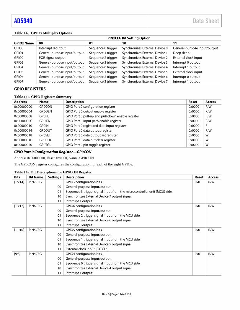
AD5940 Data Sheet
Rev. 0 | Page 114 of 130
Table 146. GPIOx Multiplex Options
GPIOx Name PINxCFG Bit Setting Option
00 01 10 11 GPIO0 Interrupt 0 output Sequence 0 trigger Synchronizes External Device 0 General-purpose input/output GPIO1 General-purpose input/output Sequence 1 trigger Synchronizes External Device 1 Deep sleep GPIO2 POR signal output Sequence 2 trigger Synchronizes External Device 2 External clock input GPIO3 General-purpose input/output Sequence 3 trigger Synchronizes External Device 3 Interrupt 0 output GPIO4 General-purpose input/output Sequence 0 trigger Synchronizes External Device 4 Interrupt 1 output GPIO5 General-purpose input/output Sequence 1 trigger Synchronizes External Device 5 External clock input GPIO6 General-purpose input/output Sequence 2 trigger Synchronizes External Device 6 Interrupt 0 output GPIO7 General-purpose input/output Sequence 3 trigger Synchronizes External Device 7 Interrupt 1 output
GPIO REGISTERS
Table 147. GPIO Registers Summary Address Name Description Reset Access 0x00000000 GP0CON GPIO Port 0 configuration register 0x0000 R/W 0x00000004 GP0OEN GPIO Port 0 output enable register 0x0000 R/W 0x00000008 GP0PE GPIO Port 0 pull-up and pull-down enable register 0x0000 R/W 0x0000000C GP0IEN GPIO Port 0 input path enable register 0x0000 R/W 0x00000010 GP0IN GPIO Port 0 registered data input register 0x0000 R 0x00000014 GP0OUT GPIO Port 0 data output register 0x0000 R/W 0x00000018 GP0SET GPIO Port 0 data output set register 0x0000 W 0x0000001C GP0CLR GPIO Port 0 data out clear register 0x0000 W 0x00000020 GP0TGL GPIO Port 0 pin toggle register 0x0000 W
GPIO Port 0 Configuration Register—GP0CON
Address 0x00000000, Reset: 0x0000, Name: GP0CON
The GP0CON register configures the configuration for each of the eight GPIOs.
Table 148. Bit Descriptions for GP0CON Register Bits Bit Name Settings Description Reset Access [15:14] PIN7CFG GPIO 7configuration bits. 0x0 R/W 00 General-purpose input/output. 01 Sequence 3 trigger signal input from the microcontroller unit (MCU) side. 10 Synchronizes External Device 7 output signal. 11 Interrupt 1 output. [13:12] PIN6CFG GPIO6 configuration bits. 0x0 R/W 00 General-purpose input/output. 01 Sequence 2 trigger signal input from the MCU side. 10 Synchronizes External Device 6 output signal. 11 Interrupt 0 output. [11:10] PIN5CFG GPIO5 configuration bits. 0x0 R/W 00 General-purpose input/output. 01 Sequence 1 trigger signal input from the MCU side. 10 Synchronizes External Device 5 output signal. 11 External clock input (EXTCLK). [9:8] PIN4CFG GPIO4 configuration bits. 0x0 R/W 00 General-purpose input/output. 01 Sequence 0 trigger signal input from the MCU side. 10 Synchronizes External Device 4 output signal. 11 Interrupt 1 output.
Data Sheet AD5940
Rev. 0 | Page 115 of 130
Bits Bit Name Settings Description Reset Access [7:6] PIN3CFG GPIO3 configuration bits. 0x0 R/W 00 General-purpose input/output. 01 Sequence 3 trigger signal input from the MCU side. 10 Synchronizes External Device 3 output signal. 11 Interrupt 0 output. [5:4] PIN2CFG GPIO2 configuration bits. 0x0 R/W 00 POR signal output. 01 Sequence 2 trigger signal input from the MCU side. 10 Synchronizes External Device 2 output signal. 11 External clock input (EXTCLK). [3:2] PIN1CFG GPIO1 configuration bits. 0x0 R/W 00 General-purpose input/output. 01 Sequence 1 trigger signal input from the MCU side. 10 Synchronizes External Device 1 output signal. 11 Deep sleep. Sleep flag indicating that the AD5940 is in hibernate mode. Used when
reading data FIFO. When the MCU receives the FIFO full or almost full interrupt, the MCU waits for this pin to go high. Then, the MCU wakes the AD5940 and reads data FIFO. After the data FIFO is read, the MCU sends a command to put the AD5940 back in sleep mode.
[1:0] PIN0CFG GPIO0 configuration bits. 0x0 R/W 00 Interrupt 0 output. 01 Sequence 0 trigger signal input from the MCU side. 10 Synchronizes External Device 0 output signal. 11 General-purpose input/output.
GPIO Port 0 Output Enable Register—GP0OEN
Address 0x00000004, Reset: 0x0000, Name: GP0OEN
The GP0OEN register enables the output for each GPIO.
Table 149. Bit Descriptions for GP0OEN Register Bits Bit Name Settings Description Reset Access [15:8] Reserved Reserved. 0x0 R [7:0] OEN Pin output drive enable. Each bit in this range is set to enable the output for that
particular pin. Each bit is cleared to disable the output for each pin. 0x0 R/W
GPIO Port 0 Pull-Up and Pull-Down Enable Register—GP0PE
Address 0x00000008, Reset: 0x0000, Name: GP0PE
Table 150. Bit Descriptions for GP0PE Register Bits Bit Name Settings Description Reset Access [15:8] Reserved Reserved. 0x0 R [7:0] PE Pin pull enable. Each bit in this range is set to enable the pull-up and/or pull-down
resistor for that particular pin. Each bit is cleared to disable the pull-up/pull-down resistor for each pin.
0x0 R/W
GPIO Port 0 Input Path Enable Register—GP0IEN
Address 0x0000000C, Reset: 0x0000, Name: GP0IEN
Table 151. Bit Descriptions for GP0IEN Register Bits Bit Name Settings Description Reset Access [15:8] RESERVED Reserved. 0x0 R [7:0] IEN Input path enable. Each bit is set to enable the input path and cleared to disable the
input path for the GPIOx pin. 0x0 R/W
AD5940 Data Sheet
Rev. 0 | Page 116 of 130
GPIO Port 0 Registered Data Input—GP0IN
Address 0x00000010, Reset: 0x0000, Name: GP0IN
Table 152. Bit Descriptions for GP0IN Register Bits Bit Name Settings Description Reset Access [15:8] Reserved Reserved. 0x0 R [7:0] IN Registered data input. Each bit reflects the state of the GPIOx pin if the
corresponding input buffer is enabled. If the pin input buffer is disabled the value seen is zero.
0x0 R
GPIO Port 0 Data Output Register—GP0OUT
Address 0x00000014, Reset: 0x0000, Name: GP0OUT
Table 153. Bit Descriptions for GP0OUT Register Bits Bit Name Settings Description Reset Access [15:8] Reserved Reserved. 0x0 R [7:0] OUT Data out. Set by user code to drive the corresponding GPIOx high. Cleared by user to
drive the corresponding GPIOx low. 0x0 R/W
GPIO Port 0 Data Out Set Register—GP0SET
Address 0x00000018, Reset: 0x0000, Name: GP0SET
Table 154. Bit Descriptions for GP0SET Register Bits Bit Name Settings Description Reset Access [15:8] Reserved Reserved. 0x0 R [7:0] Set Set the output high. Set by user code to drive the corresponding GPIOx high.
Clearing this bit has no effect. 0x0 W
GPIO Port 0 Data Out Clear Register—GP0CLR
Address 0x0000001C, Reset: 0x0000, Name: GP0CLR
Table 155. Bit Descriptions for GP0CLR Register Bits Bit Name Settings Description Reset Access [15:8] Reserved Reserved. 0x0 R [7:0] CLR Set the output low. Each bit is set to drive the corresponding GPIOx pin low.
Clearing this bit has no effect. 0x0 W
GPIO Port 0 Pin Toggle Register—GP0TGL
Address 0x00000020, Reset: 0x0000, Name: GP0TGL
Table 156. Bit Descriptions for GP0TGL Register Bits Bit Name Settings Description Reset Access [15:8] Reserved Reserved 0x0 R [7:0] TGL Toggle the Output. Each bit is set to invert the corresponding GPIOx pin. Clearing
this bit has no effect. 0x0 W
Data Sheet AD5940
Rev. 0 | Page 117 of 130
SYSTEM RESETS The AD5940 provides the following reset sources:
• External reset. • POR. • Software reset of the digital part of the device. The low
power PA and low power TIA circuitry is not reset.
The AD5940 is reset during an external hardware reset or POR.
The external reset or hardware reset is connected to the external RESET pin. When this pin is pulled low, a reset occurs. All circuits and control registers return to their default state.
The host microcontroller can trigger a software reset to the AD5940 by clearing SWRSTCON, Bit 0. It is recommends to connect the RESET pin of the AD5940 to a GPIO pin on the host processor to give the controller control over hardware resets.
The AD5940 reset status register is RSTSTA. Read this register to identify the source of the reset to the chip.
Software resets can be bypassed to ensure the circuits used to bias an external sensor are not disturbed. These circuits include the ultra low power DACs, power amplifier, and TIAs. The programmable switches circuits can also be configured to maintain their states in the event of a reset.
ANALOG DIE RESET REGISTERS
Table 157. Analog Die Reset Registers Summary Address Name Description Reset Access 0x00000A5C RSTCONKEY Key protection for SWRSTCON register. 0x0000 W 0x00000424 SWRSTCON Software reset register. 0x0001 R/W 0x00000A40 RSTSTA Reset status register. 0x0000 R/W1C
Key Protection for the RSTCON Register—RSTCONKEY
Address 0x00000A5C, Reset: 0x0000, Name: RSTCONKEY
Table 158. Bit Descriptions for RSTCONKEY Register Bits Bit Name Settings Description Reset Access [15:0] Key Reset control key register. The SWRSTCON register is key protected with a value of 0x12EA.
Write to the SWRSTCON register after the key is entered. A write to any other register before writing to the SWRSTCON register returns the protection to the lock state.
0x0 W
Software Reset Register—SWRSTCON
Address 0x00000424, Reset: 0x0001, Name: SWRSTCON
Table 159. Bit Descriptions for SWRSTCON Register Bits Bit Name Settings Description Reset Access [15:1] Reserved Reserved. 0x0 R 0 SWRSTL Software reset. Write to the RESTCONKEY register to unlock this register. 0x1 R/W 0 Not reset. 0xA158 Trigger reset.
Reset Status Register—RSTSTA
Address 0x00000A40, Reset: 0x0000, Name: RSTSTA
Table 160. Bit Descriptions for RSTSTA Register Bits Bit Name Settings Description Reset Access [15:4] Reserved Reserved. 0x0 R
3 MMRSWRST MMR software reset. This bit is automatically set to 1 when writing to the SWRSTCON register. Clear this bit by writing 1.
0x0 R/W1C
2 Reserved Reserved. 0x0 R/W1C
1 EXTRST External reset. This bit is automatically set to 1 when an external reset occurs. Clear this bit by writing 1.
0x0 R/W1C
0 POR AFE power-on reset. This bit is automatically set when a POR occurs. Clear this bit by writing 1.
0x0 R/W1C
AD5940 Data Sheet
Rev. 0 | Page 118 of 130
POWER MODES There are four main power modes for the AD5940: active high power mode (>80 kHz), active normal mode (<80 kHz), hibernate mode, and shutdown mode.
ACTIVE HIGH POWER MODE (>80 kHz) Active high power mode (>80 kHz) is recommended when generating or measuring high bandwidth signals >80 kHz. The 32 MHz oscillator is selected to drive the high speed DAC and ADC circuits to handle the high bandwidth signal. To enable high power mode, use the following sequence:
1. Write PMBW = 0x000D. 2. Set the system clock divider to 2 and set the ADC clock
divider to 1. 3. Switch the oscillator to 32 MHz. 4. Set ADCFILTERCON, Bit 0 = 1 to enable a 1.6 MHz ADC
sample rate.
ACTIVE LOW POWER MODE (<80 kHz) Active low power mode (<80 kHz) is the default active state of the AD5940. The system clock is the 16 MHz internal oscillator (PWRMOD, Bits[1:0] = 0x1).
HIBERNATE MODE When the AD5940 is in hibernate mode, the high speed clock circuits are powered down, resulting in all blocks being clocked when entering a low power, clock gated state. The 32 kHz oscillator remains active. The watchdog timer is also active. To place the AD5940 in hibernate mode, write PWRMOD, Bits[1:0] = 0x2. It is recommended that PWRMOD, Bit 14 = 0. Bit 14 controls a power switch to the ADC block. When this switch is turned off,
the leakage from the ADC is reduced, which subsequently reduces the current consumption in hibernate mode.
Optionally, the low power DAC, reference, and amplifiers can remain active to maintain the bias of an external sensor. However, current consumption increases.
SHUTDOWN MODE Shutdown mode is similar to hibernate, except the user is expected to power-down the low power analog blocks.
LOW POWER MODE The AD5940 provides a feature for ultra low power applications, such as EDA measurements. Various blocks can be powered down simultaneously by writing to the LPMODECON register. Within the LPMODECON register, there are a number of bits corresponding to certain analog blocks. By setting these bits to 1, the corresponding piece of circuitry is powered down to save power. For example, writing 1 to LPMODECON, Bit 1, powers down the high power reference.
The LPMODECON register features key protection. Before accessing the register, the user must write 0xC59D6 to the LPMODEKEY register.
Another feature that is useful in ultra low power applications is the ability to switch system clocks to the 32 kHz oscillator using the sequencer. To enable this feature, write 1 to LPMODECLKSEL, Bit 0. The sequencer can then switch the system clocks to the 32 kHz oscillator. The LPMODECLKSEL register is key protected by the LPMODKEY register.
POWER MODES REGISTERS
Table 161. Power Mode Registers Summary Address Name Description Reset Access 0x00000A00 PWRMOD Power mode configuration register 0x0001 R/W 0x00000A04 PWRKEY Key protection for PWRMOD register 0x0000 R/W 0x0000210C LPMODEKEY Key protection for LPMODECLKSEL and LPMODECON registers 0x00000000 R/W 0x00002110 LPMODECLKSEL Low power mode clock select register 0x00000000 R/W 0x00002114 LPMODECON Low power mode configuration register 0x00000102 R/W
Power Modes Register—PWRMOD
Address 0x00000A00, Reset: 0x0001, Name: PWRMOD
Table 162. Bit Descriptions for PWRMOD Register Bits Bit Name Settings Description Reset Access 15 RAMRETEN Retention for RAM. 0x0 R/W 0 RAM is not retained during hibernate mode. 1 RAM is retained during hibernate mode. 14 ADCRETEN This bit keeps the ADC power switch on in hibernate mode. 0x0 R/W 0 ADC power switch turned off during hibernate mode. 1 ADC power switch turned on during hibernate mode. [13:4] Reserved Reserved. 0x0 R
Data Sheet AD5940
Rev. 0 | Page 119 of 130
Bits Bit Name Settings Description Reset Access 3 SEQSLPEN Autosleep function by sequencer command. 0x0 R/W 0 Disables the sequencer autosleep function. 1 Enables the sequencer autosleep function. 2 TMRSLPEN Autosleep function by sleep and wake-up timer. 0x0 R/W 0 Disables the sleep and wake-up timer autosleep function. 1 Enables the sleep and wake-up timer autosleep function. [1:0] PWRMOD Power mode control bits. When read, these bits contain the last power mode value
entered by user code. 0x1 R/W
01 Active mode. Normal working mode. All digital circuits powered up. The user can optionally power down blocks by disabling their input clock.
10 Hibernate mode. Digital core powered down. Most AFE die blocks powered down (low power DACs and references can remain active to bias an external sensor). SRAM is powered down, with or without retention. The high speed clock is powered down. Only the low speed clock is powered up.
11 Reserved.
Key Protection for the PWRMOD Register—PWRKEY
Address 0x00000A04, Reset: 0x0000, Name: PWRKEY
Table 163. Bit Descriptions for PWRKEY Register Bits Bit Name Settings Description Reset Access [15:0] PWRKEY PWRMOD key register. The PWRMOD register is key protected. Two writes to the key
are necessary to change the value in the PWRMOD register: first 0x4859, then 0xF27B. Then, write to the PWRMOD register. A write to any other register before writing to PWRMOD returns the protection to the lock state.
0x0 R/W
Low Power Mode AFE Control Lock Register—LPMODEKEY
Address 0x0000210C, Reset: 0x00000000, Name: LPMODEKEY
The LPMODEKEY register protects the LPMODECLKSEL and LPMODECON registers.
Table 164. Bit Descriptions for LPMODEKEY Register Bits Bit Name Settings Description Reset Access [31:20] Reserved Reserved. 0x0 R [19:0] Key These bits are the key for low power mode control by the sequencer related
registers. The key prevents accidental writing to the registers. 0x0 R/W
0xC59D6 Clocks related registers via a sequencer write. 0x00000 Locks the clock related registers via a sequencer write. Write any value other than
0xC59D6 to lock the sequencer read/write clock related registers.
Low Power Mode Clock Select Register—LPMODECLKSEL
Address 0x00002110, Reset: 0x00000000, Name: LPMODECLKSEL
The LPMODECLKSEL register is protected by the LPMODKEY register.
Table 165. Bit Descriptions for LPMODECLKSEL Register Bits Bit Name Settings Description Reset Access [31:1] Reserved Reserved. 0x0 R 0 LFSYSCLKEN Enable for switching the system clock to 32 kHz via the sequencer. Write 1 to this
bit to switch to the 32 kHz oscillator. Clear this bit to switch to the 16 MHz oscillator. 0x0 R/W
AD5940 Data Sheet
Rev. 0 | Page 120 of 130
Low Power Mode Configuration Register—LPMODECON
Address 0x00002114, Reset: 0x00000102, Name: LPMODECON
The LPMODECON register is protected by the LPMODEKEY register.
Table 166. Bit Descriptions for LPMODECON Register Bits Bit Name Settings Description Reset Access [31:9] Reserved Reserved. 0x0 R 8 ALDOEN Set this bit high to power-down the analog LDO. 0x1 R/W 7 V1P1HSADCEN Set this bit high to enable the 1.11 V high speed common-mode buffer. 0x0 R/W 6 V1P8HSADCEN Set this bit high to enable the high speed 1.82 V reference buffer. 0x0 R/W [5:4] RESERVED Reserved. 0x0 R/W 3 REPEATADCCNVEN_P Set this bit high to enable the repetition of ADC conversions. 0x0 R/W 2 ADCCONVEN Set this bit high to enable ADC conversions. 0x0 R/W 1 HSREFDIS Set this bit high to power-down the high speed reference. 0x1 R/W 0 HFOSCPD Set this bit high to power-down the high speed power oscillator. 0x0 R/W
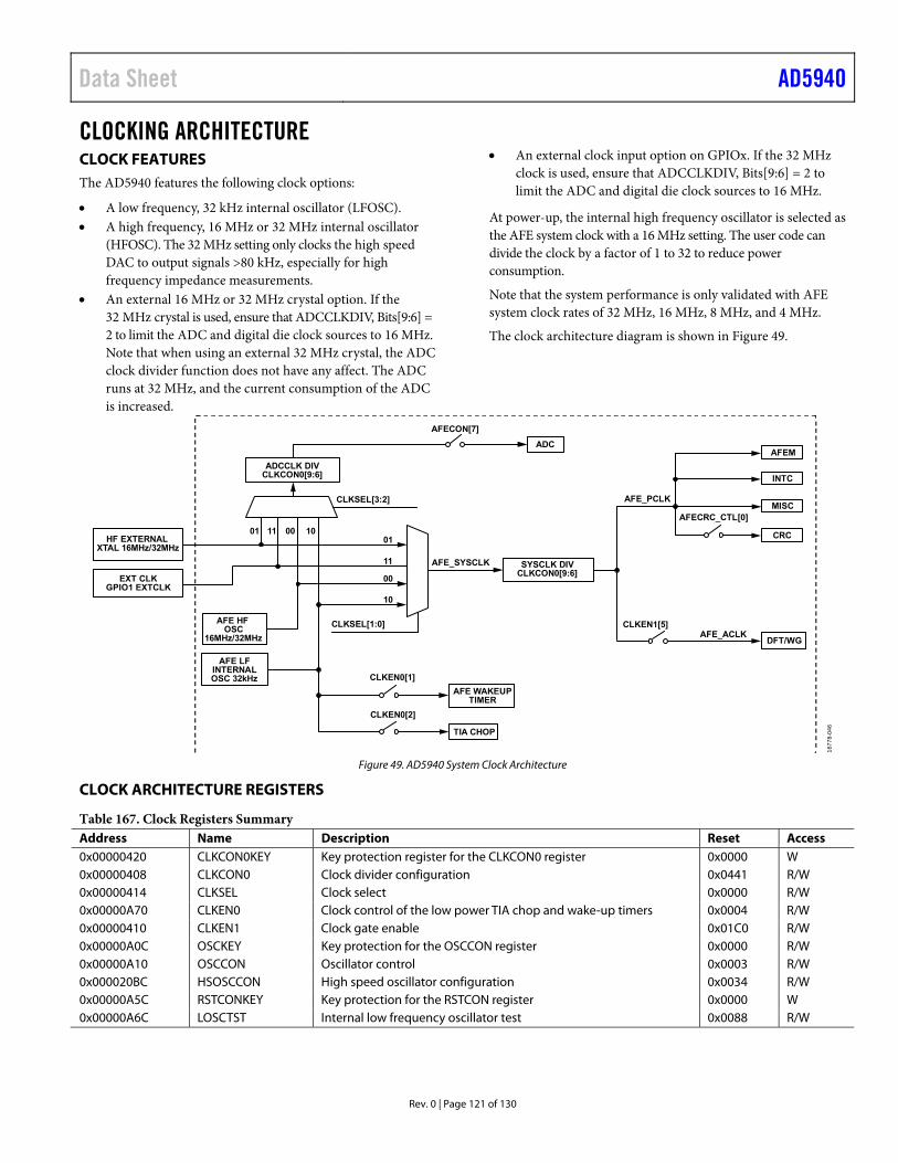
Data Sheet AD5940
Rev. 0 | Page 121 of 130
CLOCKING ARCHITECTURE CLOCK FEATURES The AD5940 features the following clock options:
A low frequency, 32 kHz internal oscillator (LFOSC). A high frequency, 16 MHz or 32 MHz internal oscillator
(HFOSC). The 32 MHz setting only clocks the high speed DAC to output signals >80 kHz, especially for high frequency impedance measurements.
An external 16 MHz or 32 MHz crystal option. If the 32 MHz crystal is used, ensure that ADCCLKDIV, Bits[9:6] = 2 to limit the ADC and digital die clock sources to 16 MHz. Note that when using an external 32 MHz crystal, the ADC clock divider function does not have any affect. The ADC runs at 32 MHz, and the current consumption of the ADC is increased.
An external clock input option on GPIOx. If the 32 MHz clock is used, ensure that ADCCLKDIV, Bits[9:6] = 2 to limit the ADC and digital die clock sources to 16 MHz.
At power-up, the internal high frequency oscillator is selected as the AFE system clock with a 16 MHz setting. The user code can divide the clock by a factor of 1 to 32 to reduce power consumption.
Note that the system performance is only validated with AFE system clock rates of 32 MHz, 16 MHz, 8 MHz, and 4 MHz.
The clock architecture diagram is shown in Figure 49.
HF EXTERNALXTAL 16MHz/32MHz
EXT CLKGPIO1 EXTCLK
AFE HFOSC
16MHz/32MHz
AFE LFINTERNALOSC 32kHz
SYSCLK DIVCLKCON0[9:6]
AFE_SYSCLK
ADCCLK DIVCLKCON0[9:6]
ADC
CLKSEL[1:0]
CLKSEL[3:2]
AFE WAKEUPTIMER
TIA CHOP
CLKEN0[1]
CLKEN0[2]
CRC
MISC
INTC
AFEM
AFE_PCLK
DFT/WG
CLKEN1[5]AFE_ACLK
00
01
10
11
0001 1011
AFECON[7]
AFECRC_CTL[0]
1677
8-04
6
Figure 49. AD5940 System Clock Architecture
CLOCK ARCHITECTURE REGISTERS
Table 167. Clock Registers Summary Address Name Description Reset Access 0x00000420 CLKCON0KEY Key protection register for the CLKCON0 register 0x0000 W 0x00000408 CLKCON0 Clock divider configuration 0x0441 R/W 0x00000414 CLKSEL Clock select 0x0000 R/W 0x00000A70 CLKEN0 Clock control of the low power TIA chop and wake-up timers 0x0004 R/W 0x00000410 CLKEN1 Clock gate enable 0x01C0 R/W 0x00000A0C OSCKEY Key protection for the OSCCON register 0x0000 R/W 0x00000A10 OSCCON Oscillator control 0x0003 R/W 0x000020BC HSOSCCON High speed oscillator configuration 0x0034 R/W 0x00000A5C RSTCONKEY Key protection for the RSTCON register 0x0000 W 0x00000A6C LOSCTST Internal low frequency oscillator test 0x0088 R/W
AD5940 Data Sheet
Rev. 0 | Page 122 of 130
Key Protection Register for the CLKCON0 Register—CLKCON0KEY
Address 0x00000420, Reset: 0x0000, Name: CLKCON0KEY
Table 168. Bit Descriptions for CLKCON0KEY Register Bits Bit Name Settings Description Reset Access [15:0] KEY Write 0xA815 to this register before accessing the CLKCON0 register 0x0 W
Clock Divider Configuration Register—CLKCON0
Address 0x00000408, Reset: 0x0441, Name: CLKCON0
Table 169. Bit Descriptions for CLKCON0 Register Bits Bit Name Settings Description Reset Access [15:10] Reserved Reserved. Do not write to these bits. 0x1 R/W [9:6] ADCCLKDIV ADC clock divider configuration. The ADC clock divider provides a divided clock from a
16 MHz root clock that drives the ADC clock. The ADC clock frequency (fADC) = root clock/ADCCLKDIV. The value range is from 1 to 15. Values of 0 and 1 have the same results as divide by 1. The fADC frequency must be ≤32 MHz. The ADC is only evaluated with a 16 MHz and 32 MHz ADC clock.
0x1 R/W
[5:0] SYSCLKDIV System clock divider configuration. The system clock divider provides a divided clock from a 16 MHz root clock that drives most digital peripherals. The system clock frequency (fSYS) = root clock/SYSCLKDIV. The value range is from 1 to 32. Values larger than 32 are saturated to 32. Values of 0 and 1 have the same results as divide by 1. The fSYS frequency must be ≤16 MHz.
0x1 R/W
Clock Select Register—CLKSEL
Address 0x00000414, Reset: 0x0000, Name: CLKSEL
Table 170. Bit Descriptions for CLKSEL Register Bits Bit Name Settings Description Reset Access [15:4] Reserved Reserved. 0x0 R [3:2] ADCCLKSEL Selects the ADC clock source. 0x0 R/W 0 Internal high frequency oscillator clock. 1 External high frequency crystal clock. 10 Internal low frequency oscillator clock (not recommended). 11 External clock. [1:0] SYSCLKSEL Selects system clock source. 0x0 R/W 0 Internal high frequency oscillator clock. 1 External high frequency crystal clock. 10 Internal low frequency oscillator clock (not recommended). 11 External clock.
Clock Enable for Low Power TIA Chop and Wake-Up Timer—CLKEN0
Address 0x00000A70, Reset: 0x0004, Name: CLKEN0
Table 171. Bit Descriptions for CLKEN0 Register Bits Bit Name Settings Description Reset Access [15:3] Reserved Reserved. 0x0 R 2 TIACHSDIS TIA chop clock disable. 0x1 R/W 0 Turn on TIA chop clock. 1 Turn off TIA chop clock. 1 SLPWUTDIS Sleep and wake-up timer clock disable. 0x0 R/W 0 Turn on sleep wake-up timer clock. 1 Turn off sleep wake-up timer clock. 0 Reserved Reserved. 0x0 R/W
Data Sheet AD5940
Rev. 0 | Page 123 of 130
Clock Gate Enable Register—CLKEN1
Address 0x00000410, Reset: 0x01C0, Name: CLKEN1
Table 172. Bit Descriptions for CLKEN1 Register Bits Bit Name Settings Description Reset Access [15:10] Reserved Reserved. 0x0 R 9 Reserved Reserved. Never write to this bit. Leave this bit cleared to 0. 0x0 R/W 8 Reserved Reserved. Never write to this bit. 0x1 R/W [7:6] Reserved Reserved. Always leave at 0. Never write to these bits. 0x1 R/W 5 ACLKDIS ACLK clock enable. This bit controls the main AFE control clock, including the analog
interface and digital signal processing. 0x0 R/W
1 Turn off ACLK clock. 0 Turn on ACLK clock. 4 Reserved Reserved. Always leave at 0. Never write to this bit. 0x0 R/W 3 Reserved Write 1 to this bit at initialization. 0x0 R/W 2 Reserved Reserved. Always leave at 0. Never write to this bit. 0x0 R/W 1 Reserved Reserved. Always leave at 0. Never write to this bit. 0x0 R/W 0 Reserved Write 1 to this bit at initialization. 0x0 R/W
Key Protection for the OSCCON Register—OSCKEY
Address 0x00000A0C, Reset: 0x0000, Name: OSCKEY
Table 173. Bit Descriptions for OSCKEY Register Bits Bit Name Settings Description Reset Access [15:0] OSCKEY Oscillator control key register. The OSCCON register is key protected. OSCKEY must be
written to with a value of 0xCB14 before accessing the OSCCON register. A write to any other register before writing to the OSCCON register returns the protection to the lock state.
0x0 R/W
Oscillator Control Register—OSCCON
Address 0x00000A10, Reset: 0x0003, Name: OSCCON
The OSCCON register is key protected. To unlock this protection, write 0xCB14 to the OSCKEY register before writing to this register. A write to any other register before writing to this register returns the protection to the lock state.
Table 174. Bit Descriptions for OSCCON Register Bits Bit Name Settings Description Reset Access [15:11] Reserved Reserved. 0x0 R 10 HFXTALOK Status of the high frequency crystal oscillator. This bit indicates when the oscillator is
stable after it is enabled. This bit is not a monitor and does not indicate a subsequent loss of stability.
0x0 R
0 Oscillator is not yet stable or is disabled. 1 Oscillator is enabled and is stable and ready for use. 9 HFOSCOK Status of the high frequency oscillator. This bit indicates when the oscillator is stable
after it is enabled. This bit is not a monitor and does not indicate a subsequent loss of stability.
0x0 R
0 Oscillator is not yet stable or is disabled. 1 Oscillator is enabled and is stable and ready for use. 8 LFOSCOK Status of the low frequency oscillator. This bit indicates when the oscillator is stable
after it is enabled. This bit is not a monitor and does not indicate a subsequent loss of stability.
0x0 R
0 Oscillator is not yet stable or is disabled. 1 Oscillator is enabled and is stable and ready for use. [7:3] Reserved Reserved. 0x0 R
AD5940 Data Sheet
Rev. 0 | Page 124 of 130
Bits Bit Name Settings Description Reset Access 2 HFXTALEN High frequency crystal oscillator enable. This bit is used to enable and disable the
oscillator. The oscillator must be stable before use. This bit must be set before the SYSRESETREQ system reset can be initiated.
0x0 R/W
0 The high frequency crystal oscillator is disabled and placed in a low power state. 1 The high frequency crystal oscillator is enabled. 1 HFOSCEN High frequency internal oscillator enable. This bit is used to enable and disable the
oscillator. The oscillator must be stable before use. This bit must be set before the SYSRESETREQ system reset can be initiated.
0x1 R/W
0 The high frequency oscillator is disabled and placed in a low power state. 1 The high frequency oscillator is enabled. 0 LFOSCEN Low frequency internal oscillator enable. This bit is used to enable and disable the
oscillator. The oscillator must be stable before use. 0x1 R/W
0 The low frequency oscillator is disabled and placed in a low power state. 1 The low frequency oscillator is enabled.
High Power Oscillator Configuration Register—HSOSCCON
Address 0x000020BC, Reset: 0x00000034, Name: HSOSCCON
Table 175. Bit Descriptions for HSOSCCON Register Bits Bit Name Settings Description Reset Access [31:3] Reserved Reserved. 0x3 R 2 CLK32MHZEN 16 MHz/32 MHz output selector signal. This bit determines if the output is 32 MHz
or 16 MHz. The ADC can run at 32 MHz, but system clock cannot run at 32 MHz. It is required to divide the system clock by 2 first before switching the oscillator to 32 MHz. Refer to the SYSCLKDIV bit in the CLKCON0 register.
0x1 R/W
0 Select 32 MHz output. 1 Select 16 MHz output. [1:0] Reserved Reserved. 0x0 R
Key Protection for RSTCON Register—RSTCONKEY
Address 0x00000A5C, Reset: 0x0000, Name: RSTCONKEY
Table 176. Bit Descriptions for RSTCONKEY Register Bits Bit Name Settings Description Reset Access [15:0] KEY Reset control key register. SWRSTCON is key protected with a value of 0x12EA. Write to
the SWRSTCON register after the key is entered. A write to any other register before writing to SWRSTCON returns the protection to the lock state.
0x0 W
Internal Low Frequency Oscillator Register—LOSCTST
Address 0x00000A6C, Reset: 0x0088, Name: LOSCTST
Table 177. Bit Descriptions for LOSCTST Register Bits Bit Name Settings Description Reset Access [15:4] Reserved Reserved. 0x8 R/W [3:0] TRIM Trim capacitors to adjust frequency. The output frequency can be trimmed by
adjusting the charging capacitors. 0x8 R/W
Data Sheet AD5940
Rev. 0 | Page 125 of 130
APPLICATIONS INFORMATION EDA BIOIMPEDANCE MEASUREMENT USING A LOW BANDWIDTH LOOP The AD5940 can be used for EDA measurements. This use case requires an always on measurement with a typical sampling rate of 4 Hz and excitation signal of 100 Hz. The AD5940 uses the low power DAC to generate the low frequency signal. The low power TIA converts current to voltages, and the DFT hardware
accelerators calculates the real and imaginary values of the data. A high level block diagram is shown in Figure 50. An accurate ac impedance value is then calculated. Using the low power mode features of the AD5940 can achieve an average current consumption as low as 70 μA. For details, see the AN-1557 Application Note.
AD5940
RLIMITCISO1 CE0
SE0
+
PA
–
LPDAC0WAVEFORMGENERATOR
SINC3
+
LPTIA
–
MU
X
ADC/800kHz
DFT
FIFO
LPTIA_LPF0
LPF0
RFILTER
VCEO
SW10
LPTIA_N
SW2
ZUNKNOWN
RTIA
CISO2
PRECISIONREFERENCE
1677
8-04
7
Figure 50. Low Frequency, 2-Wire, Bioimpedance Loop (Maximum Bandwidth = 300 Hz)
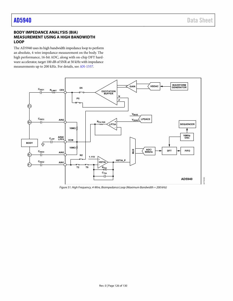
AD5940 Data Sheet
Rev. 0 | Page 126 of 130
BODY IMPEDANCE ANALYSIS (BIA) MEASUREMENT USING A HIGH BANDWIDTH LOOP The AD5940 uses its high bandwidth impedance loop to perform an absolute, 4-wire impedance measurement on the body. The high performance, 16-bit ADC, along with on-chip DFT hard-ware accelerator, target 100 dB of SNR at 50 kHz with impedance measurements up to 200 kHz. For details, see AN-1557.
GAIN
EXCITATIONBUFFER
+
HSTIA–
ADC/800kHz DFT FIFO
16MHzOSC
SEQUENCER
AIN2
AIN3
AIN1
CE0
MU
X
10MΩ
10MΩ
RLIMIT
T2 T9
N2
D5
P5
VCM
HSTIA_P
AD5940
CISO1
1.11V
BODY
CISO3
CISO4
CISO2
AIN4/LPF0CLPF
HSDAC WAVEFORMGENERATOR
LPDAC0+
LPTIA–
VZERO
VBIAS
RFILTER
RTIA
CTIA
S+
S–
F+
F–
1677
8-05
2
N
P
Figure 51. High Frequency, 4-Wire, Bioimpedance Loop (Maximum Bandwidth = 200 kHz)
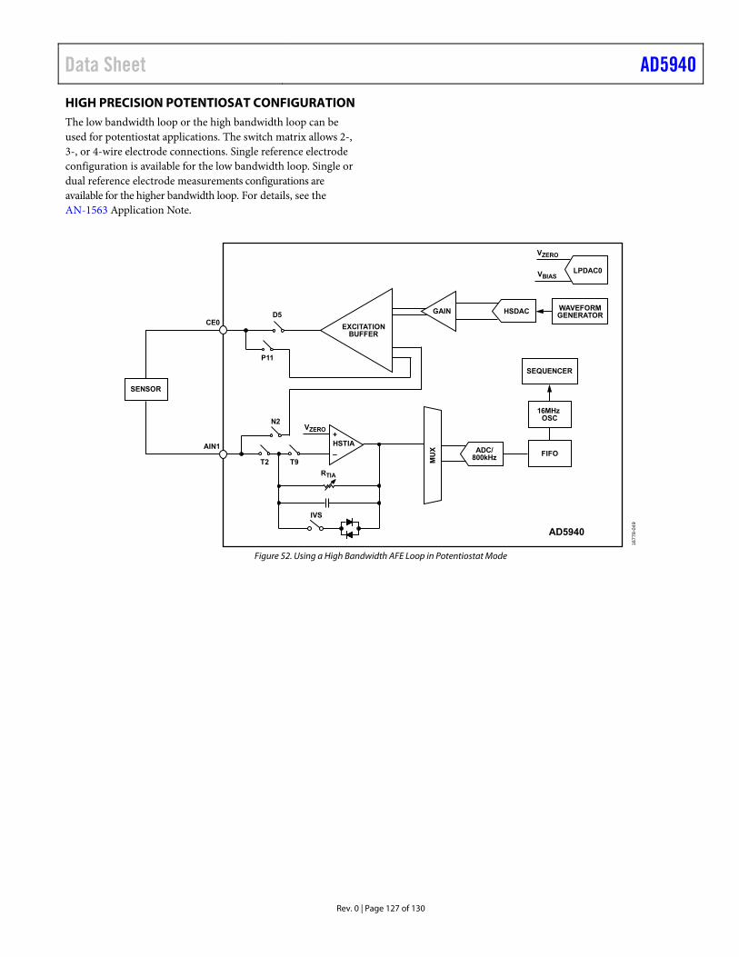
Data Sheet AD5940
Rev. 0 | Page 127 of 130
HIGH PRECISION POTENTIOSAT CONFIGURATION The low bandwidth loop or the high bandwidth loop can be used for potentiostat applications. The switch matrix allows 2-, 3-, or 4-wire electrode connections. Single reference electrode configuration is available for the low bandwidth loop. Single or dual reference electrode measurements configurations are available for the higher bandwidth loop. For details, see the AN-1563 Application Note.
LPDAC0
GAIN
EXCITATIONBUFFER
HSDAC WAVEFORMGENERATOR
+HSTIA
–ADC/
800kHz FIFO
16MHzOSC
SEQUENCER
AIN1
CE0
MU
X
VBIAS
VZERO
T2 T9
N2
D5
P11
AD5940
VZERO
SENSOR
RTIA
IVS
1677
8-04
9
Figure 52. Using a High Bandwidth AFE Loop in Potentiostat Mode
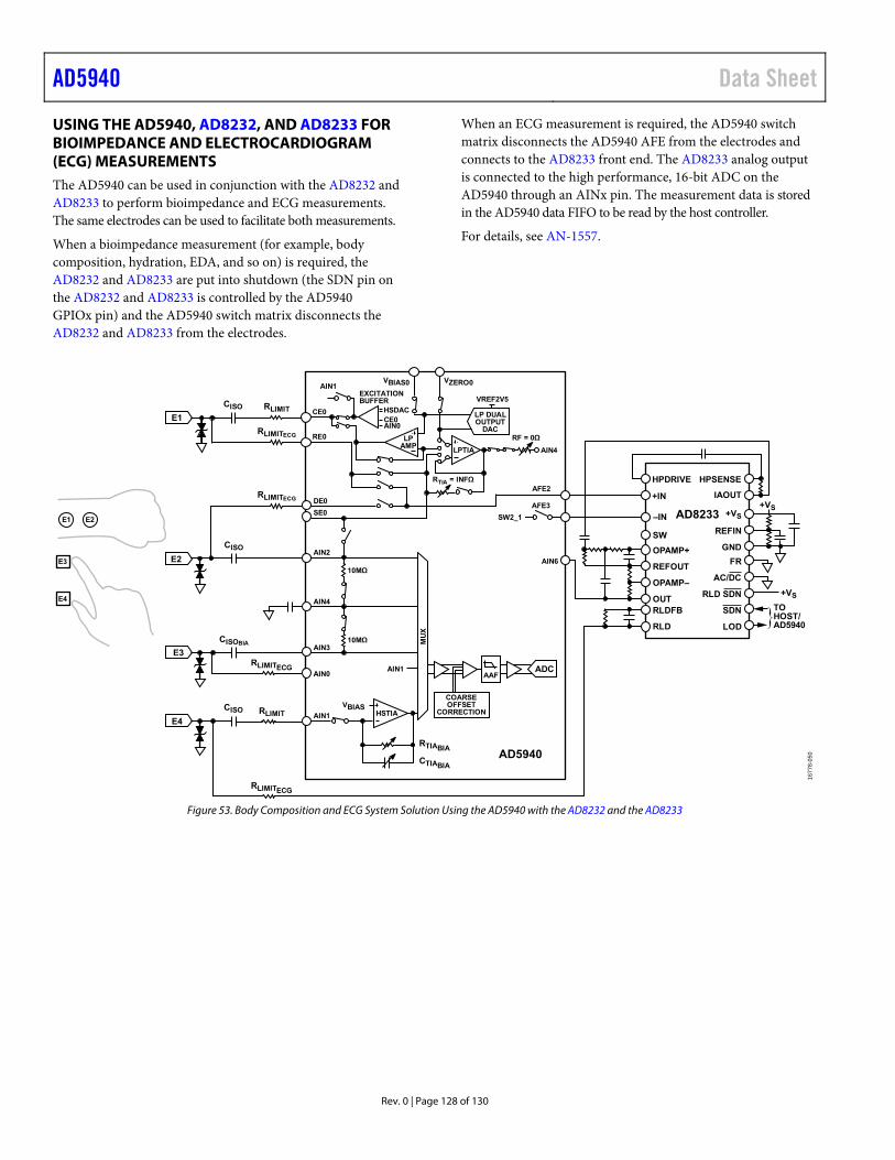
AD5940 Data Sheet
Rev. 0 | Page 128 of 130
USING THE AD5940, AD8232, AND AD8233 FOR BIOIMPEDANCE AND ELECTROCARDIOGRAM (ECG) MEASUREMENTS The AD5940 can be used in conjunction with the AD8232 and AD8233 to perform bioimpedance and ECG measurements. The same electrodes can be used to facilitate both measurements.
When a bioimpedance measurement (for example, body composition, hydration, EDA, and so on) is required, the AD8232 and AD8233 are put into shutdown (the SDN pin on the AD8232 and AD8233 is controlled by the AD5940 GPIOx pin) and the AD5940 switch matrix disconnects the AD8232 and AD8233 from the electrodes.
When an ECG measurement is required, the AD5940 switch matrix disconnects the AD5940 AFE from the electrodes and connects to the AD8233 front end. The AD8233 analog output is connected to the high performance, 16-bit ADC on the AD5940 through an AINx pin. The measurement data is stored in the AD5940 data FIFO to be read by the host controller.
For details, see AN-1557.
E3
E4
E1 E2
E1
E4
RLIMITCISO
CISO
CISOBIA
RLIMITECG
RLIMITECG
CISO
RLIMITECG
RTIABIA
CTIABIA
RLIMITECG
RLIMIT
HPDRIVE HPSENSE
IAOUT
+VS
+VS
+VS
REFIN
TOHOST/AD5940
AD8233
GND
FR
AC/DC
RLD SDN
SDN
LOD
+IN
–IN
SW
RLD
RLDFB
OPAMP+
REFOUT
OPAMP–
OUT
AAF
VBIASAIN1
AIN1
AIN2
CE0
AIN1
RE0
DE0
SE0
AIN4
AIN3
AIN0
MU
X
10MΩ
10MΩ
ADC
COARSEOFFSET
CORRECTIONHSTIA
LPTIA
VREF2V5
RF = 0Ω
RTIA = INFΩ
AIN4
LPAMP
HSDAC
EXCITATIONBUFFER
VBIAS0 VZERO0
CE0AIN0
LP DUALOUTPUT
DAC
AIN6
AFE3
AFE2
SW2_1
AD5940
1677
8-05
0
E3
E2
Figure 53. Body Composition and ECG System Solution Using the AD5940 with the AD8232 and the AD8233
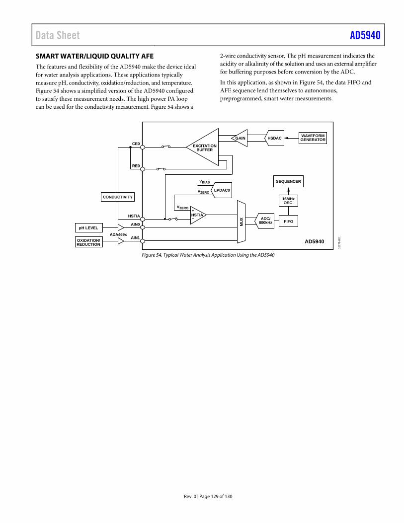
Data Sheet AD5940
Rev. 0 | Page 129 of 130
SMART WATER/LIQUID QUALITY AFE The features and flexibility of the AD5940 make the device ideal for water analysis applications. These applications typically measure pH, conductivity, oxidation/reduction, and temperature. Figure 54 shows a simplified version of the AD5940 configured to satisfy these measurement needs. The high power PA loop can be used for the conductivity measurement. Figure 54 shows a
2-wire conductivity sensor. The pH measurement indicates the acidity or alkalinity of the solution and uses an external amplifier for buffering purposes before conversion by the ADC.
In this application, as shown in Figure 54, the data FIFO and AFE sequence lend themselves to autonomous, preprogrammed, smart water measurements.
GAIN
EXCITATIONBUFFER
+HSTIA– ADC/
800kHz FIFO
16MHzOSC
SEQUENCER
HSTIA
AIN0
AIN1
CE0
MU
XAD5940
CONDUCTIVITY
pH LEVEL
OXIDATION/REDUCTION
HSDAC WAVEFORMGENERATOR
ADA469x
LPDAC0VZERO
VZERO
VBIAS
RE0
1677
8-05
1
Figure 54. Typical Water Analysis Application Using the AD5940
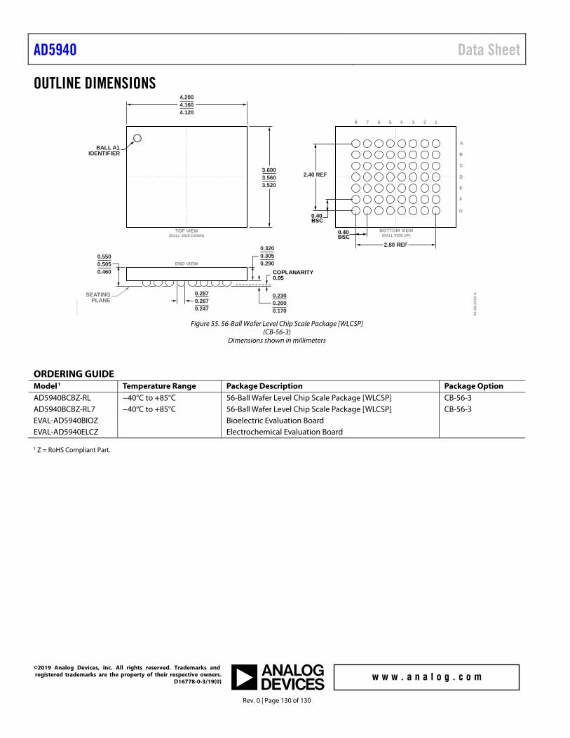
AD5940 Data Sheet
Rev. 0 | Page 130 of 130
OUTLINE DIMENSIONS
04-0
6-20
18-A
PKG
-005
910
4.2004.1604.120
3.6003.5603.520
12345678
2.40 REF
2.80 REF
0.40BSC
0.40BSC
BALL A1IDENTIFIER
0.5500.5050.460
0.3200.3050.290
0.2300.2000.170
0.2870.2670.247
COPLANARITY0.05
SEATINGPLANE
BOTTOM VIEW(BALL SIDE UP)
TOP VIEW(BALL SIDE DOWN)
END VIEW
A
B
C
D
E
F
G
Figure 55. 56-Ball Wafer Level Chip Scale Package [WLCSP] (CB-56-3)
Dimensions shown in millimeters
ORDERING GUIDE Model1 Temperature Range Package Description Package Option AD5940BCBZ-RL −40°C to +85°C 56-Ball Wafer Level Chip Scale Package [WLCSP] CB-56-3 AD5940BCBZ-RL7 −40°C to +85°C 56-Ball Wafer Level Chip Scale Package [WLCSP] CB-56-3 EVAL-AD5940BIOZ Bioelectric Evaluation Board EVAL-AD5940ELCZ Electrochemical Evaluation Board
1 Z = RoHS Compliant Part.
©2019 Analog Devices, Inc. All rights reserved. Trademarks and registered trademarks are the property of their respective owners.
D16778-0-3/19(0)