high-power,wide voltage range, quad ...wide voltage range, quad-portethernet power sourcing...
TRANSCRIPT
www.ti.com
FEATURES APPLICATIONS
DESCRIPTION
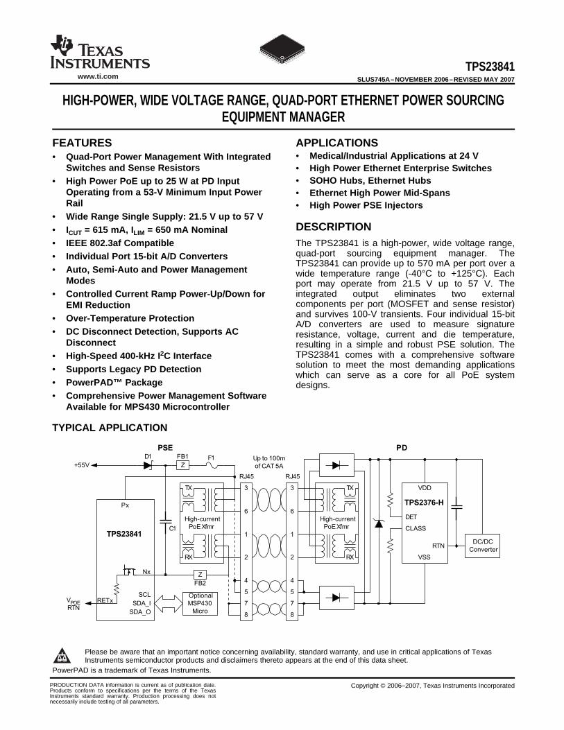
TYPICAL APPLICATION
F1D1
Z
Z
RETx
Nx
Px
TPS23841CLASS
DET
VDD
VSS
RTN
TPS2376-H
Optional
MSP430
Micro
DC/DC
Converter
SDA_O
SDA_I
SCL
+55V
VPOERTN
High-current
PoEXfmr
High-current
PoEXfmr
3
6
1
2
7
8
RJ45
4
5
3
6
1
2
7
8
RJ45
4
5
TX
RX
TX
RX
Up to 100m
of CAT 5A
FB1
FB2
C1
PSE PD
TPS23841SLUS745A–NOVEMBER 2006–REVISED MAY 2007
HIGH-POWER, WIDE VOLTAGE RANGE, QUAD-PORT ETHERNET POWER SOURCINGEQUIPMENT MANAGER
• Medical/Industrial Applications at 24 V• Quad-Port Power Management With IntegratedSwitches and Sense Resistors • High Power Ethernet Enterprise Switches
• SOHO Hubs, Ethernet Hubs• High Power PoE up to 25 W at PD InputOperating from a 53-V Minimum Input Power • Ethernet High Power Mid-SpansRail • High Power PSE Injectors
• Wide Range Single Supply: 21.5 V up to 57 V• ICUT = 615 mA, ILIM = 650 mA Nominal• IEEE 802.3af Compatible The TPS23841 is a high-power, wide voltage range,
quad-port sourcing equipment manager. The• Individual Port 15-bit A/D ConvertersTPS23841 can provide up to 570 mA per port over a
• Auto, Semi-Auto and Power Management wide temperature range (-40°C to +125°C). EachModes port may operate from 21.5 V up to 57 V. The
integrated output eliminates two external• Controlled Current Ramp Power-Up/Down forcomponents per port (MOSFET and sense resistor)EMI Reductionand survives 100-V transients. Four individual 15-bit• Over-Temperature ProtectionA/D converters are used to measure signature
• DC Disconnect Detection, Supports AC resistance, voltage, current and die temperature,Disconnect resulting in a simple and robust PSE solution. The
TPS23841 comes with a comprehensive software• High-Speed 400-kHz I2C Interfacesolution to meet the most demanding applications• Supports Legacy PD Detectionwhich can serve as a core for all PoE system
• PowerPAD™ Package designs.• Comprehensive Power Management Software
Available for MPS430 Microcontroller
Please be aware that an important notice concerning availability, standard warranty, and use in critical applications of TexasInstruments semiconductor products and disclaimers thereto appears at the end of this data sheet.
PowerPAD is a trademark of Texas Instruments.
PRODUCTION DATA information is current as of publication date. Copyright © 2006–2007, Texas Instruments IncorporatedProducts conform to specifications per the terms of the TexasInstruments standard warranty. Production processing does notnecessarily include testing of all parameters.

www.ti.com
DESCRIPTION (CONTINUED)
TPS23841SLUS745A–NOVEMBER 2006–REVISED MAY 2007
The TPS23841 has three internal supply buses (10 V, 6.3 V and 3.3 V) generated from the 48-V input supply.These supplies are used to bias all internal digital and analog circuitry. Each supply has been brought outseparately for proper bypassing to insure high performance. The digital supply (3.3 V) is available for poweringexternal loads up to 2 mA. For more demanding loads it is highly recommended to use external buffers toprevent system degradation. When the TPS23841 is initially powered up an internal Power-on-Reset (POR)circuit resets all registers and sets all ports to the off state to ensure that the device is powered up in a knownsafe operating state.
The TPS23841 has three modes of operation; auto mode (AM), semi-auto mode (SAM) and power managementmode (PMM).• In auto mode the TPS23841 performs discovery, classification and delivery of power autonomously to a
compliant PD without the need of a micro-controller.• In semi-auto mode the TPS23841 operates in auto mode but users can access the contents of all read status
registers and A/D registers through the I2C serial interface. All write control registers are active except for D0through D3 of port control register 1 (Address 0010) for limited port control. The semi-auto mode allows theTPS23841 to detect valid PD's without micro-controller intervention but adds a flexibility to perform powermanagement activities.
• Power management mode (with a micro-controller) allows users additional capabilities of discoveringnon-compliant (legacy) PDs, performing AC Disconnect and advanced power management system controlthat are based on real time port voltages and currents. All functions in this mode are programmed andcontrolled through read/write registers over the I2C interface. This allows users complete freedom indetecting and powering devices. A comprehensive software package is available that mates the power of theTPS23841 with the MSP430 micro-controller.
TPS23841 integrated output stage provides port power and low-side control. The internal low-side circuitry isdesigned with internal current sensing so there are no external resistors required. The output design ensures thepower switches operate in the fully enhanced mode for low power dissipation.
The I2C interface allows easy application of opto-coupler circuitry to maintain Ethernet port isolation when aground based micro-controller is required. The TPS23841 five address pins (A1–A5) allow the device to beaddressed at one of 31 possible I2C addresses. Per-port write registers separately control each port state(discovery, classification, legacy, power up, etc) while the read registers contain status information of the entireprocess along with parametric values of discovery, classification, and real-time port operating current, voltageand die temperature.
The proprietary 15-bit integrating A/D converter is designed to meet the harsh environment where the PSEPMresides. The converter is set for maximum rejection of power line noise allowing it to make accuratemeasurements of line currents during discovery, classification and power delivery for reliable powermanagement decisions.
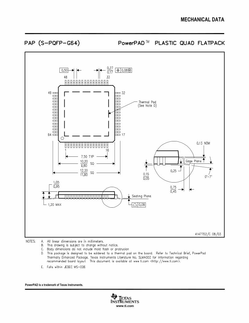
The TPS23841 is available in either 64-pin PowerPAD™ down (PAP) or 64-pin PowerPAD up (PJD) packages.
ORDERING INFORMATION
TEMPERATURE RANGE PACKAGED DEVICES (1)
TA = TJ TQFP – 64 (PAP) (2) TQFP – 64 (PJD) (2)
–40°C to 125°C TPS23841PAP TPS23841PJD
(1) The PAP and PJD packages are available taped and reeled. Add R suffix to device type(e.g.TPS23841PAPR) to order quantities of 1,000 devices per reel.
(2) PAP = PowerPad down, PJD = PowerPad up.
2 Submit Documentation Feedback
www.ti.com
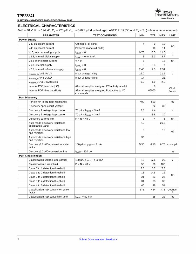
ABSOLUTE MAXIMUM RATINGS
DISSIPATION RATINGS (1)
RECOMMENDED OPERATING CONDITIONS
ELECTRO STATIC DISCHARGE (ESD) PROTECTION
TPS23841SLUS745A–NOVEMBER 2006–REVISED MAY 2007
over operating free-air temperature range (unless otherwise noted) (1) (2)
PARAMETER VALUE UNIT
V10 current sourced 100 µA
V3.3 current sourced 5 mA
Applied voltage on CINT#, CT, RBIAS –0.5 to 10
Applied voltage on SCL, SDA_I, SDA_O, INTB, A1, A2, A3, A4, A5, MS, PORB, WD_DIS, –0.5 to 6 VALT_A/B, AC_LO, AC_HI
Applied voltage on V48, P#, N# –0.5 to 80
TJ Junction operating temperature –40 to 125
Tstg Storage temperature --55 to 150 –55 to 150 °C
Tsol Lead temperature (soldering, 10 sec.) 260
(1) Stresses beyond those listed under absolute maximum ratings may cause permanent damage to the device. These are stress ratingsonly, and functional operation of the device at these or any other conditions beyond those indicated under recommended operatingconditions is not implied. Exposure to absolute-maximum-rated conditions for extended periods may affect device reliability.
(2) All voltages are with respect to GND. Currents are positive into, negative out of the specified terminal. Consult Packaging Section of theData book for thermal limitations and considerations of packages.
THERMAL RESISTANCE THERMAL RESISTANCEPACKAGE JUNCTION TO CASE θJC JUNCTION TO AMBIENT θJA
PAP 0.38°C/W 21.47°C/W
PJD 0.38°C/W 21.47°C/W
(1) Thermal Resistance measured using 2-oz copper trace and copper pad solder following layout recommendation in TI PublicationPowerPAD Thermally Enhanced Package Technical Brief SLMA002.
over operating free-air temperature range (unless otherwise noted)
PARAMETER MIN NOM MAX UNIT
VIN Input voltage, V48 pin 21.5 48 57 V
TJ Junction temperature -40 125 °C
MAX UNIT
Human body model 1.5
CDM 1 kV
Machine model 0.2
3Submit Documentation Feedback
www.ti.com
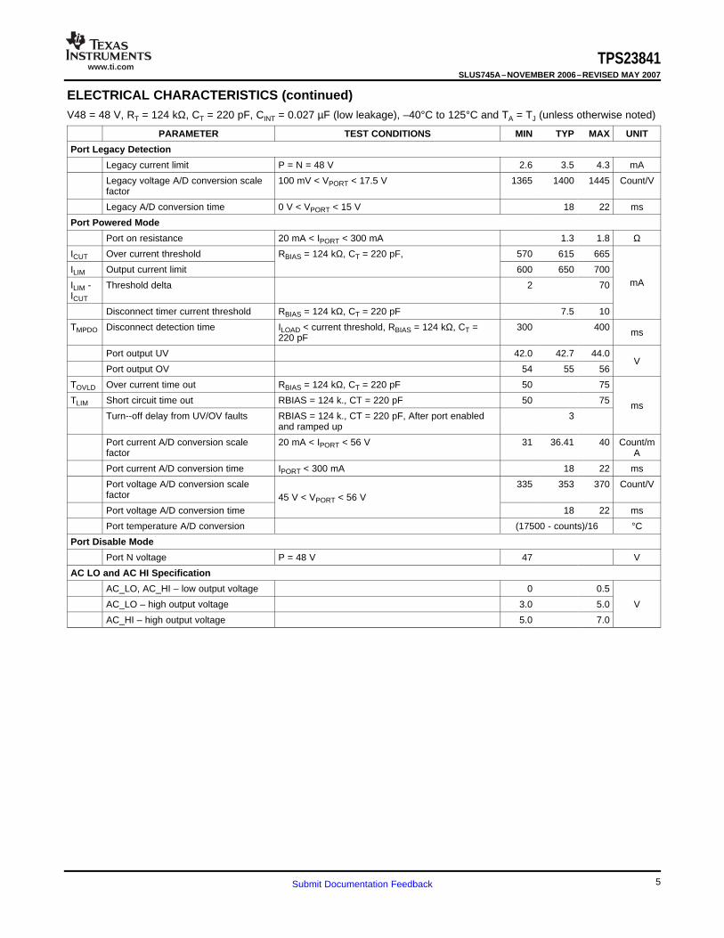
ELECTRICAL CHARACTERISTICS
TPS23841SLUS745A–NOVEMBER 2006–REVISED MAY 2007
V48 = 48 V, RT = 124 kΩ, CT = 220 pF, CINT = 0.027 µF (low leakage), –40°C to 125°C and TA = TJ (unless otherwise noted)
PARAMETER TEST CONDITIONS MIN TYP MAX UNIT
Power Supply
V48 quiescent current Off mode (all ports) 4 9 12mA
V48 quiescent current Powered mode (all ports) 10 14
V10, internal analog supply ILOAD = 0 9.75 10.5 11.5V
V3.3, internal digital supply ILOAD = 0 to 3 mA 3 3.3 3.7
V3.3 short circuit current V = 0 3 12 mA
V6.3, internal supply ILOAD = 0 5 6.3 7
V2.5, internal reference supply ILOAD = 0 2.46 2.5 2.54
VUVLO_R, V48 UVLO Input voltage rising 16.0 21.5 V
VUVLO_F, V48 UVLO Input voltage falling 14 21
VHYSUV, UVLO hysteresis 0.2 1.0 2.0
Internal POR time out(I2C) After all supplies are good I2C activity is valid 8Clock
Internal POR time out (Port) After all supplies are good Port active to I2C 66000 Pulsescommands
Port Discovery
Port off #P to #N input resistance 400 600 kΩ
Discovery open circuit voltage 22 30
Discovery 1 voltage loop control 70 µA < IPORT < 3 mA 2.8 4.4 V
Discovery 2 voltage loop control 70 µA < IPORT < 3 mA 8.8 10
Discovery current limit P = N = 48 V 3 4 5 mA
Auto-mode discovery resistance 19 26.5acceptance Band
Auto-mode discovery resistance low 0 15 kΩend rejection
Auto-mode discovery resistance high 33end rejection
Discovery1,2 A/D conversion scale 100 µA < IPORT < 3 mA 5.30 6.10 6.75 count/µAfactor
Discovery1,2 A/D conversion time IPORT= 120 µA ms
Port Classification
Classification voltage loop control 100 µA < IPORT < 50 mA 15 17.5 20 V
Classification current limit P = N = 48 V 50 60 100
Class 0 to 1 detection threshold 5.5 6.5 7.5
Class 1 to 2 detection threshold 13 14.5 16mA
Class 2 to 3 detection threshold 21 23 25
Class 3 to 4 detection threshold 31 33 35
Class 4 to 0 detection threshold 45 48 51
Classification A/D conversion scale 375 424 475 Count/mfactor A
Classification A/D conversion time IPORT = 50 mA 18 22 ms
4 Submit Documentation Feedback
www.ti.comTPS23841
SLUS745A–NOVEMBER 2006–REVISED MAY 2007
ELECTRICAL CHARACTERISTICS (continued)V48 = 48 V, RT = 124 kΩ, CT = 220 pF, CINT = 0.027 µF (low leakage), –40°C to 125°C and TA = TJ (unless otherwise noted)
PARAMETER TEST CONDITIONS MIN TYP MAX UNIT
Port Legacy Detection
Legacy current limit P = N = 48 V 2.6 3.5 4.3 mA
Legacy voltage A/D conversion scale 100 mV < VPORT < 17.5 V 1365 1400 1445 Count/Vfactor
Legacy A/D conversion time 0 V < VPORT < 15 V 18 22 ms
Port Powered Mode
Port on resistance 20 mA < IPORT < 300 mA 1.3 1.8 Ω
ICUT Over current threshold RBIAS = 124 kΩ, CT = 220 pF, 570 615 665
ILIM Output current limit 600 650 700mAILIM - Threshold delta 2 70
ICUT
Disconnect timer current threshold RBIAS = 124 kΩ, CT = 220 pF 7.5 10
TMPDO Disconnect detection time ILOAD < current threshold, RBIAS = 124 kΩ, CT = 300 400 ms220 pF
Port output UV 42.0 42.7 44.0V
Port output OV 54 55 56
TOVLD Over current time out RBIAS = 124 kΩ, CT = 220 pF 50 75
TLIM Short circuit time out RBIAS = 124 k., CT = 220 pF 50 75 msTurn--off delay from UV/OV faults RBIAS = 124 k., CT = 220 pF, After port enabled 3
and ramped up
Port current A/D conversion scale 20 mA < IPORT < 56 V 31 36.41 40 Count/mfactor A
Port current A/D conversion time IPORT < 300 mA 18 22 ms
Port voltage A/D conversion scale 335 353 370 Count/Vfactor 45 V < VPORT < 56 VPort voltage A/D conversion time 18 22 ms
Port temperature A/D conversion (17500 - counts)/16 °C
Port Disable Mode
Port N voltage P = 48 V 47 V
AC LO and AC HI Specification
AC_LO, AC_HI – low output voltage 0 0.5
AC_LO – high output voltage 3.0 5.0 V
AC_HI – high output voltage 5.0 7.0
5Submit Documentation Feedback

www.ti.comTPS23841SLUS745A–NOVEMBER 2006–REVISED MAY 2007
ELECTRICAL CHARACTERISTICS (continued)V48 = 48 V, RT = 124 kΩ, CT = 220 pF, CINT = 0.027 µF (low leakage), –40°C to 125°C and TA = TJ (unless otherwise noted)
PARAMETER TEST CONDITIONS MIN TYP MAX UNIT
Digital I2C DC Specifications
SCL, SDA_I, A1–A5 ,WD_DIS,ALTA/B, MS, PORB logic input 1.5 Vthreshold
SCL, SDA_I input hysteresis 250mV
MS, PORB input hysteresis 150
WD_DIS, ALTA/B, MS, PORB input Input voltage 0.5 to 3 V 50 kΩpulldown resistance
A1–A5 pull-down current 10 µA
SDA_O logic high leakage Drain = 5 V 100 nA
SDA_O logic low ISINK = 10 mA 200 mV
INTB logic high leakage Drain = 6 V 10 µA
INTB logic low ISINK = 10 mA 200 mV
Digital I2C Timing
SCL clock frequency 0 400 kHz
SCL high 0.6Pulse duration
SCL low 1.3
Rise time, SCL to SDA 0.300
Fall time, SCL to SDA 0.300
Setup time, SDA to SCL 0.250µs
Hold time, SCL to SDA 0.300 0.900
Bus free time between start and stop 1.3
Setup time, SCL to start condition 0.6
Hold time, start condition to SCL 0.6
Setup time, SCL to stop condition 0.6
6 Submit Documentation Feedback

www.ti.com
TPS23841 SINGLE PORT BLOCK DIAGRAM
Two8 BitsStatus
Register
UV/OVComparators
Two8 BitsStatus
Register
AutoSeq
Logic
A2DRegisters
ResistorVoltageCurrent
&Die Temp
AnalogControlCircurty
Diff Amp(Fix Gain)
Loop Cntri AmpDetect/Class Modes
LCAPower Mode
ThermalDetector
OVIThld
OVI
Max IThld
600 kW
TPS23841SLUS745A–NOVEMBER 2006–REVISED MAY 2007
7Submit Documentation Feedback

www.ti.comTPS23841SLUS745A–NOVEMBER 2006–REVISED MAY 2007
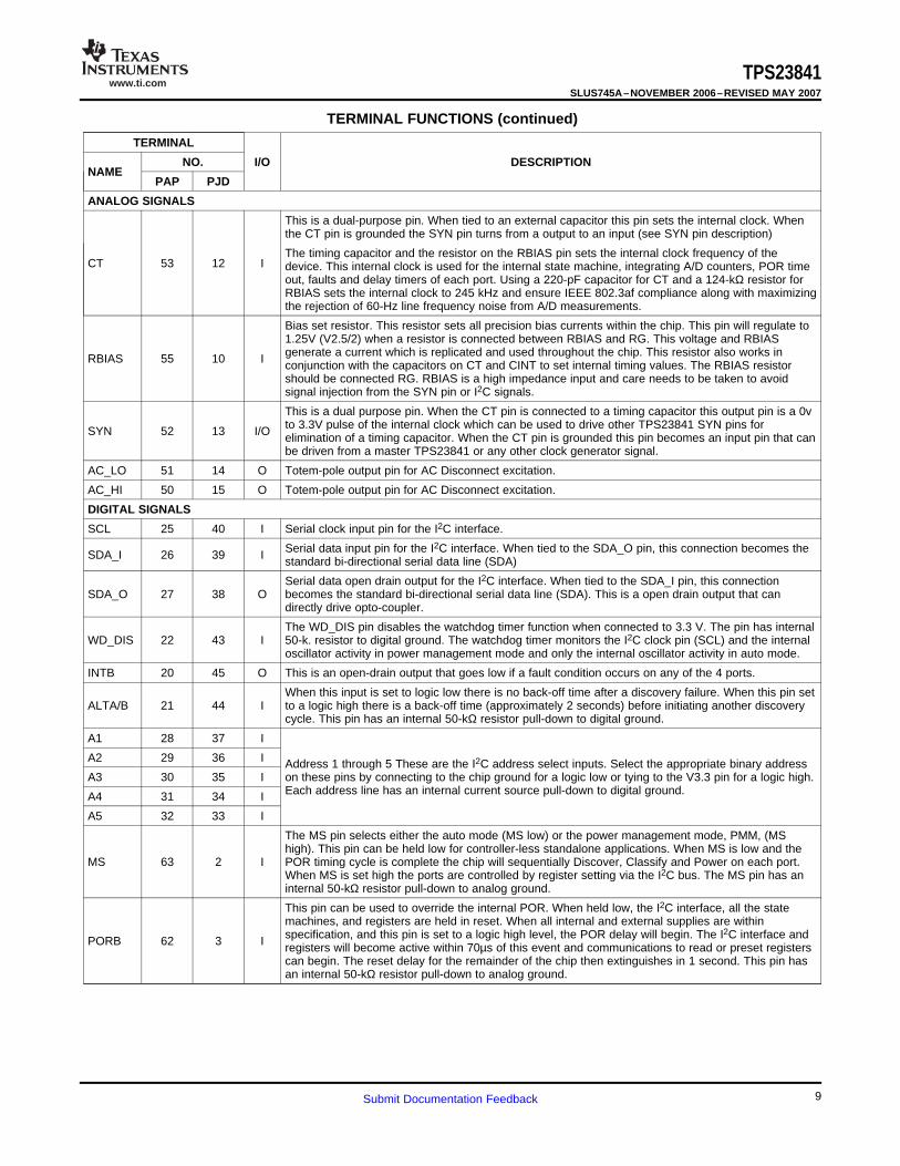
TERMINAL FUNCTIONS
TERMINAL
NO. I/O DESCRIPTIONNAME
PAP PJD
POWER AND GROUND
48-V input to the device. This supply can have a range of 22 V to 57 V. This pin should be decoupledV48 60 5 I with a 0.1-µF capacitor from V48 to AG1 placed as close to the device as possible.
10-V analog supply. The 10-V reference is generated internally and connects to the main internalV10 58 7 O analog power bus. A 0.1-µF de-coupling capacitor should terminate as close to this node and the
AG1 pin as possible. Do not use for an external supply.
6.3-V analog supply. A 0.1-µF de-coupling capacitor should terminate as close to this pin and theV6.3 59 6 O AG1 pin as possible. Do not use for an external supply.
3.3-V logic supply. The 3.3-V supply is generated internally and connects to the internal logic powerV3.3 24 41 O bus. A 0.1-µìF de-coupling capacitor should terminate as close to this node and the DG pin as
possible. This output can be used as a low current supply to external logic.
2.5-V reference supply. The V2.5 is generated internally and connects to the internal reference powerV2.5 54 11 O bus. This pin should not be tied to any external supplies. A 0.1-µF de-coupling capacitor should
terminate as close to this node and the RG pin as possible. Do not use for an external supply.
Analog ground 1. This is the analog ground of the V6.3, V10 and V48 power systems. It should beAG1 57 8 GND externally tied to the common copper 48-V return plane. This pin should carry the low side of three
de-coupling capacitors tied to V48, V10 and V6.3.
Analog ground 2. This is the analog ground which ties to the substrate and ESD structures of theAG2 61 4 GND device. It should be externally tied to the common copper 48-V return plane. AG1 and AG2 must be
tied together directly for the best noise immunity.
Digital ground. This pin connects to the internal logic ground bus. It should be externally tied to theDG 23 42 GND common copper 48-V return plane.
Reference ground. This is a precision sense of the external ground plane. The integration capacitor(CINT) and the biasing resistor (RBIAS pin) should be tied to this ground. This ground should also beRG 56 9 GND used to form a printed wiring board ground guard ring around the active node of the integrationcapacitor (CINT). It should tie to common copper 48-V return plane.
PORT ANALOG SIGNAL
P1 7 58 IPort Positive. 48-V load sense pin. Terminal voltage is monitored and controlled differentially withP2 10 55 Irespect to each Port N pin Optionally, if the application warrants, this high side path can be protected
P3 39 26 I with the use of a self resetting poly fuse.P4 42 23 I
N1 6 59 I
N2 11 54 I Port negative. 48-V load return pin. The low side of the load is switched and protected by internalcircuitry that will limit the current.N3 38 27 I
N4 43 22 I
RET1 5 60 I
RET2 12 53 I48 V return pin
RET3 37 28 I
RET4 44 21 I
CINT1 4 61 IIntegration capacitor. This capacitor is used for the ramp A/D converter signal integration. Connect A
CINT2 13 52 I 0.027- µF capacitor from this pin to RG. To minimize errors use a polycarbonate, poly-polypropylene,polystyrene or teflon capacitor type to prevent leakage. Other types of capacitors can be used withCINT3 36 29 Iincreased conversion error.
CINT4 45 20 I
8 Submit Documentation Feedback
www.ti.comTPS23841
SLUS745A–NOVEMBER 2006–REVISED MAY 2007
TERMINAL FUNCTIONS (continued)
TERMINAL
NO. I/O DESCRIPTIONNAME
PAP PJD
ANALOG SIGNALS
This is a dual-purpose pin. When tied to an external capacitor this pin sets the internal clock. Whenthe CT pin is grounded the SYN pin turns from a output to an input (see SYN pin description)
The timing capacitor and the resistor on the RBIAS pin sets the internal clock frequency of theCT 53 12 I device. This internal clock is used for the internal state machine, integrating A/D counters, POR time
out, faults and delay timers of each port. Using a 220-pF capacitor for CT and a 124-kΩ resistor forRBIAS sets the internal clock to 245 kHz and ensure IEEE 802.3af compliance along with maximizingthe rejection of 60-Hz line frequency noise from A/D measurements.
Bias set resistor. This resistor sets all precision bias currents within the chip. This pin will regulate to1.25V (V2.5/2) when a resistor is connected between RBIAS and RG. This voltage and RBIASgenerate a current which is replicated and used throughout the chip. This resistor also works inRBIAS 55 10 I conjunction with the capacitors on CT and CINT to set internal timing values. The RBIAS resistorshould be connected RG. RBIAS is a high impedance input and care needs to be taken to avoidsignal injection from the SYN pin or I2C signals.
This is a dual purpose pin. When the CT pin is connected to a timing capacitor this output pin is a 0vto 3.3V pulse of the internal clock which can be used to drive other TPS23841 SYN pins forSYN 52 13 I/O elimination of a timing capacitor. When the CT pin is grounded this pin becomes an input pin that canbe driven from a master TPS23841 or any other clock generator signal.
AC_LO 51 14 O Totem-pole output pin for AC Disconnect excitation.
AC_HI 50 15 O Totem-pole output pin for AC Disconnect excitation.
DIGITAL SIGNALS
SCL 25 40 I Serial clock input pin for the I2C interface.
Serial data input pin for the I2C interface. When tied to the SDA_O pin, this connection becomes theSDA_I 26 39 I standard bi-directional serial data line (SDA)
Serial data open drain output for the I2C interface. When tied to the SDA_I pin, this connectionSDA_O 27 38 O becomes the standard bi-directional serial data line (SDA). This is a open drain output that can
directly drive opto-coupler.
The WD_DIS pin disables the watchdog timer function when connected to 3.3 V. The pin has internalWD_DIS 22 43 I 50-k. resistor to digital ground. The watchdog timer monitors the I2C clock pin (SCL) and the internal
oscillator activity in power management mode and only the internal oscillator activity in auto mode.
INTB 20 45 O This is an open-drain output that goes low if a fault condition occurs on any of the 4 ports.
When this input is set to logic low there is no back-off time after a discovery failure. When this pin setALTA/B 21 44 I to a logic high there is a back-off time (approximately 2 seconds) before initiating another discovery
cycle. This pin has an internal 50-kΩ resistor pull-down to digital ground.
A1 28 37 I
A2 29 36 I Address 1 through 5 These are the I2C address select inputs. Select the appropriate binary addressA3 30 35 I on these pins by connecting to the chip ground for a logic low or tying to the V3.3 pin for a logic high.
Each address line has an internal current source pull-down to digital ground.A4 31 34 I
A5 32 33 I
The MS pin selects either the auto mode (MS low) or the power management mode, PMM, (MShigh). This pin can be held low for controller-less standalone applications. When MS is low and the
MS 63 2 I POR timing cycle is complete the chip will sequentially Discover, Classify and Power on each port.When MS is set high the ports are controlled by register setting via the I2C bus. The MS pin has aninternal 50-kΩ resistor pull-down to analog ground.
This pin can be used to override the internal POR. When held low, the I2C interface, all the statemachines, and registers are held in reset. When all internal and external supplies are withinspecification, and this pin is set to a logic high level, the POR delay will begin. The I2C interface andPORB 62 3 I registers will become active within 70µs of this event and communications to read or preset registerscan begin. The reset delay for the remainder of the chip then extinguishes in 1 second. This pin hasan internal 50-kΩ resistor pull-down to analog ground.
9Submit Documentation Feedback

www.ti.com
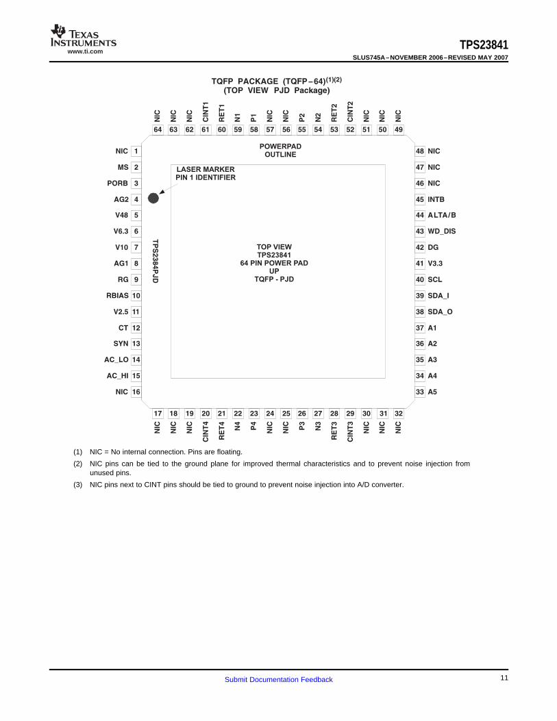
CONNECTION DIAGRAM
TPS23841
64 Pin Power Pad
TQFP_PAP
TPS23841SLUS745A–NOVEMBER 2006–REVISED MAY 2007
(1) NIC = No internal connection. Pins are floating.
(2) NIC pins can be tied to the ground plane for improved thermal characteristics and to prevent noise injection fromunused pins.
(3) NIC pins next to CINT pins should be tied to ground to prevent noise injection into A/D converter.
10 Submit Documentation Feedback
www.ti.com
LASER MARKER
PIN 1 IDENTIFIER
POWERPAD
OUTLINE
TOP VIEW
TPS23841
64 PIN POWER PAD
UP
TQFP - PJD
TPS23841SLUS745A–NOVEMBER 2006–REVISED MAY 2007
(1) NIC = No internal connection. Pins are floating.
(2) NIC pins can be tied to the ground plane for improved thermal characteristics and to prevent noise injection fromunused pins.
(3) NIC pins next to CINT pins should be tied to ground to prevent noise injection into A/D converter.
11Submit Documentation Feedback

www.ti.com
AUTO MODE FUNCTIONAL DESCRIPTION
Auto Mode
TPS23841SLUS745A–NOVEMBER 2006–REVISED MAY 2007
Auto mode (AM, MS = 0) operation is the basic approach for applying power to IEEE compliant PD’s. When AMhas been selected the TPS23841 automatically performs the following functions:• Discovery of IEEE 802.3af compliant powered devices (PD's)• Classification• Power delivery• Port over/under voltage detection, (if enabled, see Over/Under Voltage Fault section)• Port over current detection (570 mA < IPORT < 665 mA• Port maximum current limit (600 mA < IPORT < 700 mA)• DC Disconnect (5 mA < IPORT < 10 mA)• Thermal shutdown protection (TSD), (TJ > 150°C)• Internal oscillator watchdog
In AM the contents of all read registers are available via the I2C interface. In addition all control registers exceptfor the function bits can be written. This supports a semi-auto mode where the TPS23841 auto detects compliantPD's while a host can access the A/D registers and class information and then implement power management(including turning a port off, responding to faults, etc).
The write registers that are still active in AM are:• All ports disable – Common Control register 0001b• Over/Under Voltage Faults – Common Control register 0001b• Software reset – Common Control register 0001b• Disconnect disable – Port Control 1 register 0010b• Discovery fault disable – Port Control 1 register 0010b• Port enable – Port Control 2 register 0011b
For alternative B, semi-auto mode implementations which will manipulate the all ports disable or Port Enablebits, please contact the factory for additional application information.
12 Submit Documentation Feedback

www.ti.com
Auto Mode Functional Description
UpdateClass Register
PortPwrUpdate Reg
A2D V/IMeasurements
300 ms<t <400 msMPDO
OVI = Over Current FaultU/O V = Under or Over Voltage FaultTSD = Thermal Shutdown FaultTMPDO = PD Maintain Power Dropout Time LimitTED = Error Delay Timing
TPS23841SLUS745A–NOVEMBER 2006–REVISED MAY 2007
AUTO MODE FUNCTIONAL DESCRIPTION (continued)
Figure 1. The Basic Flow for Auto Mode
13Submit Documentation Feedback
www.ti.com
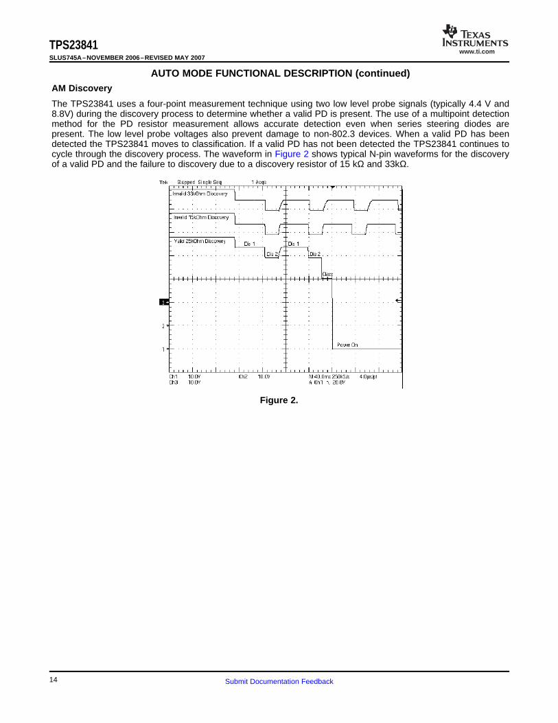
AM Discovery
TPS23841SLUS745A–NOVEMBER 2006–REVISED MAY 2007
AUTO MODE FUNCTIONAL DESCRIPTION (continued)
The TPS23841 uses a four-point measurement technique using two low level probe signals (typically 4.4 V and8.8V) during the discovery process to determine whether a valid PD is present. The use of a multipoint detectionmethod for the PD resistor measurement allows accurate detection even when series steering diodes arepresent. The low level probe voltages also prevent damage to non-802.3 devices. When a valid PD has beendetected the TPS23841 moves to classification. If a valid PD has not been detected the TPS23841 continues tocycle through the discovery process. The waveform in Figure 2 shows typical N-pin waveforms for the discoveryof a valid PD and the failure to discovery due to a discovery resistor of 15 kΩ and 33kΩ.
Figure 2.
14 Submit Documentation Feedback

www.ti.com
AM Classification
TPS23841SLUS745A–NOVEMBER 2006–REVISED MAY 2007
AUTO MODE FUNCTIONAL DESCRIPTION (continued)
After a successful discovery of a valid PD the TPS23841 enters the classification function that identifies thepower level based on the PD's current signature. The classification current level is measured at a reducedterminal voltage of 17.5V. During classification the power dissipation can be at its highest; therefore, to preventover temperature shutdown in automode only one port classifies at a time. When multiple ports successfullydiscover and proceed to classification at the same time the auto sequencer processes each request separatelyallowing only one port to enter classification. Figure 3 shows all 4 ports successfully detecting a valid PD at thesame time and than the classification of each port occurring separately.
Figure 3.
15Submit Documentation Feedback
www.ti.com
0or1
0or1or2
0or2or31 2
0 10 20 30 40 6050
4
3
2
1
0
TPS23841SLUS745A–NOVEMBER 2006–REVISED MAY 2007
AUTO MODE FUNCTIONAL DESCRIPTION (continued)
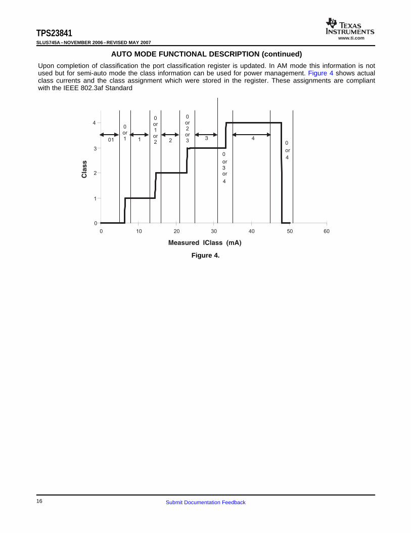
Upon completion of classification the port classification register is updated. In AM mode this information is notused but for semi-auto mode the class information can be used for power management. Figure 4 shows actualclass currents and the class assignment which were stored in the register. These assignments are compliantwith the IEEE 802.3af Standard
Figure 4.
16 Submit Documentation Feedback

www.ti.com
AM Power Delivery
AM Faults and INTB Output
TPS23841SLUS745A–NOVEMBER 2006–REVISED MAY 2007
AUTO MODE FUNCTIONAL DESCRIPTION (continued)
After successfully discovery and classification of a valid PD the power is delivered by controlling the current tothe PD until its current requirements are met or until the internal current limit is reached (approximately 650 mA).The power switch is fully enhanced after 500 µs. Figure 5 show the voltage and the current that is being appliedto the PD during power-up and reaching the PD load of 250mA.
Figure 5.
After power has been applied to the PD the TPS23841 automatically enters the current and voltage samplemode. The sample mode performs 31 current measurements and 1 voltage measurement. Each measurementtakes approximately 18 ms to complete. The port remains powered and the current/voltage measurement cyclecontinues until a fault condition occurs. The current and voltage measurements are both stored in the A/Dcurrent and voltage registers and can be accessed through the I2C pins. This allows power management in theAM if it is desired.
AM faults are:• Port under and over voltage faults, (if enabled, see Over/Under Voltage Fault section)• Over current faults• Under current (DC Disconnect) fault• Thermal shutdown (TSD) fault• Watchdog timer faults (disabled via WD_DIS pin)
Any one of the first four fault conditions listed above causes the port to shut down, and a 3-bit fault code to belatched into the affected port's Status Read 1 register (addr = 0100b). Watchdog faults cause all four ports toshut down. Faulted ports are temporarily disabled after a fault has been detected and latched.
The INTB pin is an open-drain, active-low output which is asserted if a fault condition occurs on any of the fourports. This indication is asserted for any of the port faults which result in a code displayed in the port statusregister (the faults listed in Table 8). In automode, the fault latch, the status register fault bits, and consequently,INTB assertion, are cleared by expiration of the 750-ms TED timer.
17Submit Documentation Feedback
www.ti.com
Over/Under Voltage Fault
TPS23841SLUS745A–NOVEMBER 2006–REVISED MAY 2007
AUTO MODE FUNCTIONAL DESCRIPTION (continued)
For the TPS23841, port over and undervoltge detection is disabled by default after device POR. This continuousvoltage monitoring feature can subsequently be enabled by writing a logic 1 to bit D2 in the Common Controlregister, assuming usage under the direction of a higher level controller, (i.e., usage in semi-auto mode).
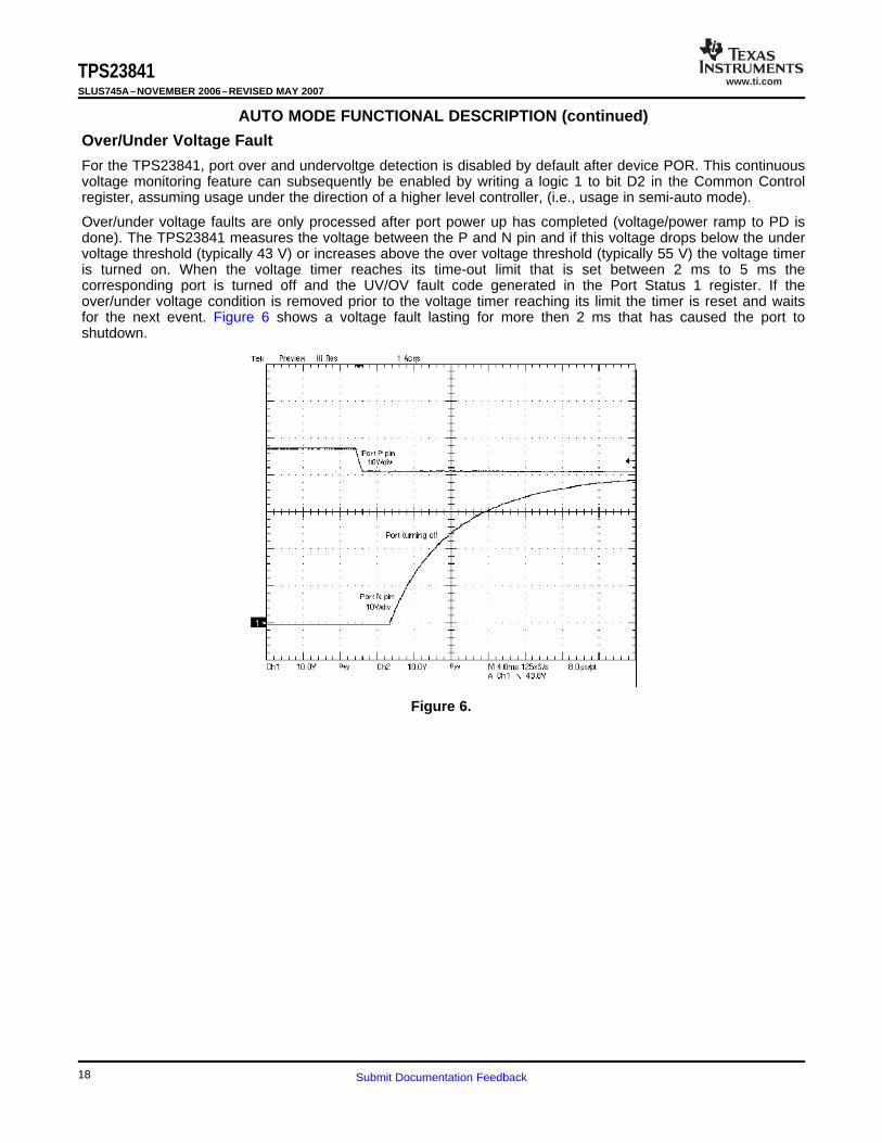
Over/under voltage faults are only processed after port power up has completed (voltage/power ramp to PD isdone). The TPS23841 measures the voltage between the P and N pin and if this voltage drops below the undervoltage threshold (typically 43 V) or increases above the over voltage threshold (typically 55 V) the voltage timeris turned on. When the voltage timer reaches its time-out limit that is set between 2 ms to 5 ms thecorresponding port is turned off and the UV/OV fault code generated in the Port Status 1 register. If theover/under voltage condition is removed prior to the voltage timer reaching its limit the timer is reset and waitsfor the next event. Figure 6 shows a voltage fault lasting for more then 2 ms that has caused the port toshutdown.
Figure 6.
18 Submit Documentation Feedback

www.ti.com
Over Current or Current Limit Faults
TPS23841SLUS745A–NOVEMBER 2006–REVISED MAY 2007
AUTO MODE FUNCTIONAL DESCRIPTION (continued)
Over current or current limit faults are conditions when the load current that is being sensed trips either the ICUTcomparator (570 mA to 665 mA) or the ILIM comparator (600 mA to 700 mA) and turns on the current fault timer.When the over current timer reaches its time out limit that is set between 50 ms to 75 ms the corresponding portis turned off and the over current fault code generated in the Port Status 1 register. If the over current conditiongoes away prior to the over current timer reaching its limit the timer is reset and waits for the next event.Figure 7 shows an over current fault lasting more than 50 ms that has caused the port to shut off.
Figure 7.
19Submit Documentation Feedback

www.ti.com
Under Current Fault (DC Modulated Disconnect)
TPS23841SLUS745A–NOVEMBER 2006–REVISED MAY 2007
AUTO MODE FUNCTIONAL DESCRIPTION (continued)
Under current fault (dc modulated disconnect) is a condition when the load current that is being measured dropsbelow 7.5mA and turns on the disconnect timer. If the disconnect timer reaches its time out limit that is setbetween 300ms to 400ms the corresponding port is turned off and the load disconnect fault code generated inthe Port Status 1 register. If the under current condition goes away prior to the disconnect timer reaching its limitthe timer is reset and the port remains powered.
Figure 8 shows DC Disconnect event. In this setup the load current was set right above the 7.5mA threshold.The duty cycle of the load was then adjusted until the off period exceeded the disconnect time out, causingturn-off of the port. The time-out period was > 300 ms.
Figure 8.
20 Submit Documentation Feedback
www.ti.com
POWER MANAGEMENT MODE FUNCTIONAL DESCRIPTION
Power Management Mode (PMM)
13 Funcitons
TPS23841SLUS745A–NOVEMBER 2006–REVISED MAY 2007
Power management mode (PMM) has been designed to work efficiently with simple low-cost microcontrollerssuch as those in the MSP430 family.
The power management mode uses 13 self-contained functions to completely control the device operation. Yousimply write/read through the I2C pins and wait for the function done bit to be set. If an A/D measurement wasperformed during the function the results can be accessed by going to the read mode and addressing the properregister.
• Disable: Disable the port and reset all functions.• Discovery 1: Enable the Discovery 1 condition which applies a 4.4 V across the PD and measure and store
the resulting current.• Discovery 2: Enable the Discovery 2 condition which applies a 8.8 V across the PD and measure and store
the resulting current.• V Sample: Measure the voltage between the P and N pins and store the result in the A/D voltage register.• Legacy: Enable the 3.5-mA current source formeasuring capacitance and measure the voltage across the P
and N terminals and store the result in the A/D voltage register.• Classify: Enable the classification condition which applies 17.7 V across the PD and measure and store the
resulting current.• Rup Pwr: Turn on the output switch while controlling the current being delivered to the PD until the PD
current needs are met or the max current is reached.• C Sample: Continuous cycle of 31 current measurements and 1 voltage measurement. After each
measurement the contents of the appropriate register are updated.• Rdwn: Turn off the output switch while controlling current until output current reaches 0 mA.• AC LO: Turns on low side output FET and measures voltage between P and N pin and store result in A/D
voltage registers.• AC HI: Turns on high side output FET and measures voltage between P and N pin and store result in A/D
voltage registers.• ISample: Measure the current and store the result in the A/D current register.• TSample: Measure the internal die temperature and store the result in the A/D temperature register.
Conversion times for A/D measurements performed as part of the functions listed above are generally asshown in the typical values in the Electrical Characteristics table. However, conversion time is somewhatdependant on the magnitude of the input signal being measured. Power management mode applicationsshould take precautions to test the A/D DONE bit (MSB of the high byte) of the pertinent results registerbefore accepting or using the returned value. A logic 1 at this bit location indicates the conversion iscomplete. Also, once an A/D conversion is in process on a given port, subsequent function calls to that portshould wait until the currently executing conversion is complete. Commands written prior to completion maycause the results of the initial conversion to be written to the register of the subsequent function.
21Submit Documentation Feedback

www.ti.com
Decoder
Dis
able
0000
Dis
cover
1
0001
Dis
cover
2
0010
VS
am
ple
0011
Legacy
0100
Cla
ssify
0101
Rup/P
wr
0110
CS
am
ple
0111
AC
LO
1001
AC
HI
1010
Rdw
n
1000
IS
am
ple
1011
TS
am
ple
1100
Pow
er
Dow
n
Measure
Chnl
I
(18m
S)
Measure
Chnl
V
(18
ms)
Apply
2.5
mA
(Vm
ax
18)
to
Chnl
Apply
AC
LO
Voltage
Measure
Chnl
I
(18m
S)
Measure
Die
Tem
pera
ture
(18m
S)
Reset
all
Functions
Apply
4.4
V
(Im
ax5m
A)
To
Chnl
Measure
Chnl
I
(18m
S)
Apply
8.8
V
(Im
ax5m
A)
To
Chnl
Measure
Chnl
V
(18m
S)
Apply
18V
(Im
ax
100m
A)
To
Chnl
Measure
Chnl
I
(18m
S)
Ram
pP
wr
1.4
A/m
Sec
Enable
OV
RI
,O
vr
V
&U
nd
V
Com
para
tors
Me
as
ure
Ch
nl
I
(31
Sa
mp
les
)S
tore
Va
lue
IR
eg
Ram
pD
ow
n
Measure
Chnl
V
(18m
S)
Apply
AC
HI
Voltage
Measure
Chnl
V
(18m
S)
Contr
ol
Regis
ter
I2C
Sto
reV
alu
e
Dis
covery
IR
eg
Set
Done
Bit
Sto
reV
alu
e
Dis
covery
IR
eg
Sto
reV
alu
e
VR
eg
Sto
reV
alu
e
VR
eg
Sto
reV
alu
e
IR
eg
4m
SD
ela
y
Sta
rtA
2D
4m
sD
ela
y
Sta
rtA
2D
Set
Done
Bit
Pw
rO
ff
Set
Done
Bit
Sto
reV
alu
e
VR
eg
Sto
reV
alu
e
VR
eg
Set
Done
Bit
Sto
reV
alu
e
Tem
pR
eg
Enable
Contr
ol
Enable
Contr
ol
Enable
DiffA
mp
Av
0.1
07
Enable
Contr
ol
Enable
Contr
ol
Latc
hS
tate
Pow
er
On
Wait
for
Next
Function
Call
Set
Done
Bit
Set
Done
Bit
Set
Done
Bit
Set
Done
Bit
Set
Done
Bit
Wait
for
Next
Function
Call
Set
Done
Bit
Cle
ar
On
Read
Wait
for
Next
Function
Call
Set
Done
Bit
Set
Done
Bit
Wait
for
Next
Function
Call
Set
Done
Bit
Note
s:
1.
Each
Functio
nS
tate
rem
ain
sset
until
anew
functio
nis
calle
d.
Exam
ple
Functio
n1
-P
ort
Volta
ge
rem
ain
sat
4.4
Vand
Resis
tor
Regis
ter
valu
eis
held
.
2.
Tim
es
show
nare
typic
aland
set
by
RB
IAS,and
CT.
3.
Poll
for
and
verify
A/D
done
indic
atio
nprior
tosendin
g
next
functio
ncall.
Wait
for
Next
Function
Call
Wait
for
Next
Function
Call
Wait
for
Next
Function
Call
If0111
Repeat
Wait
for
Next
Function
Call
Wait
for
Next
Function
Call
Wait
for
Next
Function
Call
Wait
for
Next
Function
Call
Wait
for
Next
Function
Call
Wait
for
Next
Function
Call
Me
as
ure
Ch
nl
V
(1S
am
ple
)S
tore
Va
lue
VR
eg
TPS23841SLUS745A–NOVEMBER 2006–REVISED MAY 2007
POWER MANAGEMENT MODE FUNCTIONAL DESCRIPTION (continued)
Figure 9.
22 Submit Documentation Feedback
www.ti.com
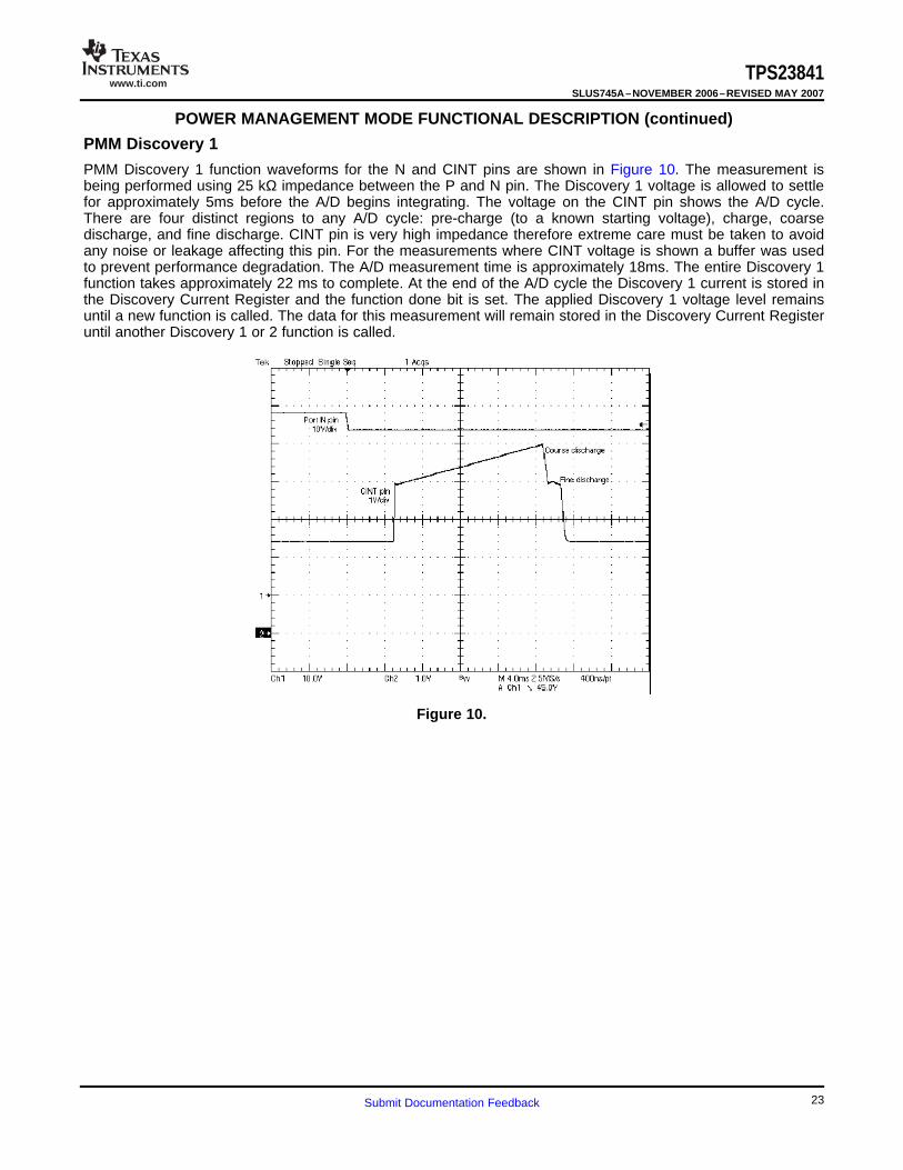
PMM Discovery 1
TPS23841SLUS745A–NOVEMBER 2006–REVISED MAY 2007
POWER MANAGEMENT MODE FUNCTIONAL DESCRIPTION (continued)
PMM Discovery 1 function waveforms for the N and CINT pins are shown in Figure 10. The measurement isbeing performed using 25 kΩ impedance between the P and N pin. The Discovery 1 voltage is allowed to settlefor approximately 5ms before the A/D begins integrating. The voltage on the CINT pin shows the A/D cycle.There are four distinct regions to any A/D cycle: pre-charge (to a known starting voltage), charge, coarsedischarge, and fine discharge. CINT pin is very high impedance therefore extreme care must be taken to avoidany noise or leakage affecting this pin. For the measurements where CINT voltage is shown a buffer was usedto prevent performance degradation. The A/D measurement time is approximately 18ms. The entire Discovery 1function takes approximately 22 ms to complete. At the end of the A/D cycle the Discovery 1 current is stored inthe Discovery Current Register and the function done bit is set. The applied Discovery 1 voltage level remainsuntil a new function is called. The data for this measurement will remain stored in the Discovery Current Registeruntil another Discovery 1 or 2 function is called.
Figure 10.
23Submit Documentation Feedback
www.ti.com
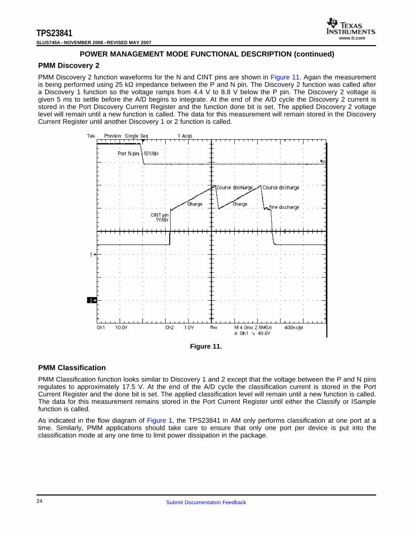
PMM Discovery 2
PMM Classification
TPS23841SLUS745A–NOVEMBER 2006–REVISED MAY 2007
POWER MANAGEMENT MODE FUNCTIONAL DESCRIPTION (continued)
PMM Discovery 2 function waveforms for the N and CINT pins are shown in Figure 11. Again the measurementis being performed using 25 kΩ impedance between the P and N pin. The Discovery 2 function was called aftera Discovery 1 function so the voltage ramps from 4.4 V to 8.8 V below the P pin. The Discovery 2 voltage isgiven 5 ms to settle before the A/D begins to integrate. At the end of the A/D cycle the Discovery 2 current isstored in the Port Discovery Current Register and the function done bit is set. The applied Discovery 2 voltagelevel will remain until a new function is called. The data for this measurement will remain stored in the DiscoveryCurrent Register until another Discovery 1 or 2 function is called.
Figure 11.
PMM Classification function looks similar to Discovery 1 and 2 except that the voltage between the P and N pinsregulates to approximately 17.5 V. At the end of the A/D cycle the classification current is stored in the PortCurrent Register and the done bit is set. The applied classification level will remain until a new function is called.The data for this measurement remains stored in the Port Current Register until either the Classify or ISamplefunction is called.
As indicated in the flow diagram of Figure 1, the TPS23841 in AM only performs classification at one port at atime. Similarly, PMM applications should take care to ensure that only one port per device is put into theclassification mode at any one time to limit power dissipation in the package.
24 Submit Documentation Feedback

www.ti.com
PMM Legacy
TPS23841SLUS745A–NOVEMBER 2006–REVISED MAY 2007
POWER MANAGEMENT MODE FUNCTIONAL DESCRIPTION (continued)
PMM Legacy function is used to detect PDs that are non compliant. Legacy detection uses a current source(typically 3.5 mA) as a test current while the A/D measures the average voltage for approximately 18 ms. Thewaveform shown in Figure 12 is the Legacy function charging a 10-µF capacitor. The capacitance charges to avalue that is no greater than 20V below the P port voltage. As the capacitor is charging the A/D is accumulatingcounts in the voltage A/D register. Figure 13 shows the relationship between port capacitance and the number ofcounts. A user can characterize non-compliant PD's signatures and use the Legacy function to recognize thesedevices.
Figure 12.
Figure 13.
25Submit Documentation Feedback
www.ti.com
PMM Rup Pwr
PMM RDWN
t - Time - s/divm
TPS23841SLUS745A–NOVEMBER 2006–REVISED MAY 2007
POWER MANAGEMENT MODE FUNCTIONAL DESCRIPTION (continued)
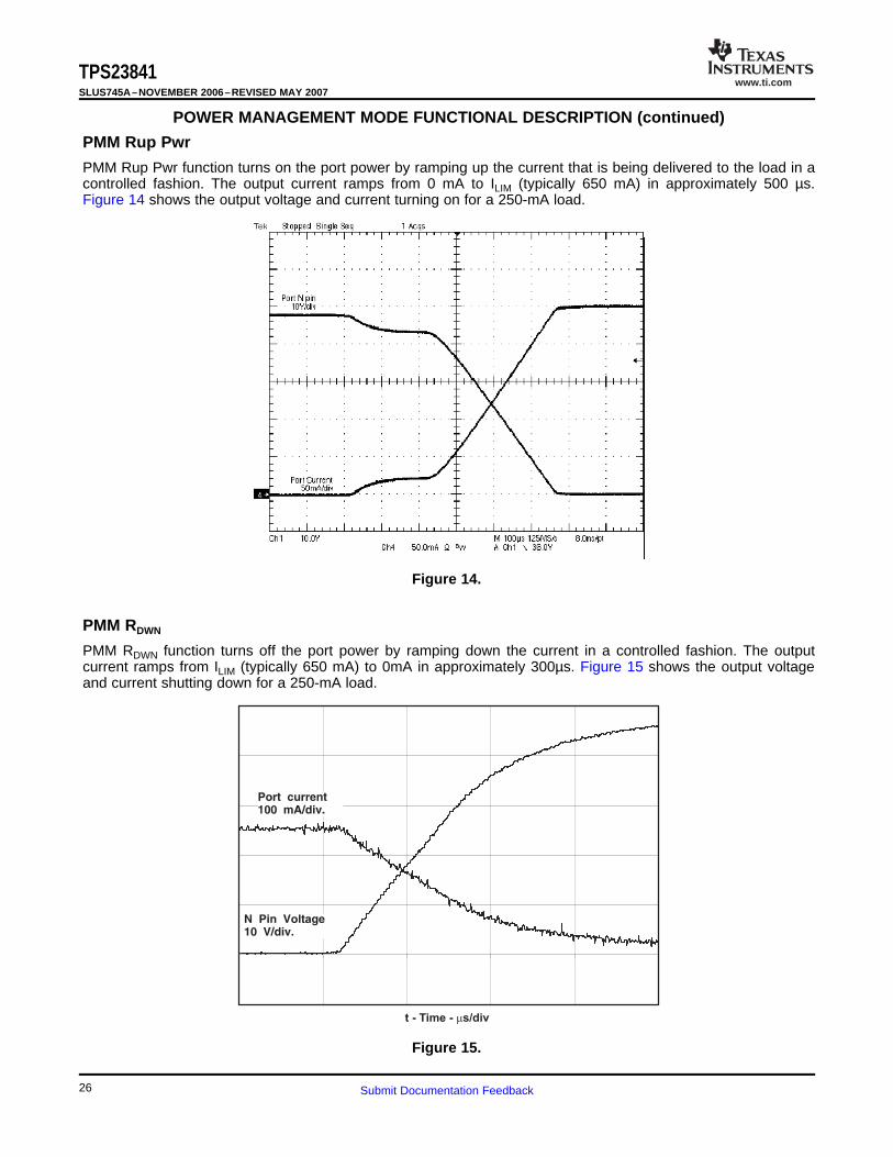
PMM Rup Pwr function turns on the port power by ramping up the current that is being delivered to the load in acontrolled fashion. The output current ramps from 0 mA to ILIM (typically 650 mA) in approximately 500 µs.Figure 14 shows the output voltage and current turning on for a 250-mA load.
Figure 14.
PMM RDWN function turns off the port power by ramping down the current in a controlled fashion. The outputcurrent ramps from ILIM (typically 650 mA) to 0mA in approximately 300µs. Figure 15 shows the output voltageand current shutting down for a 250-mA load.
Figure 15.
26 Submit Documentation Feedback

www.ti.com
Miscellaneous Functional Description
PMM Faults
Watchdog Timer
TPS23841SLUS745A–NOVEMBER 2006–REVISED MAY 2007
POWER MANAGEMENT MODE FUNCTIONAL DESCRIPTION (continued)
PMM faults are the same as those shown in the AM Faults and INTB Output section. In PM mode, the portunder- and over voltage and under-current faults can be enabled or disabled by writing to the control bits in theappropriate register. For the TPS23841, port under- and overvoltage detection is disabled by default after devicePOR or other reset operation. Under current detection, (DC Disconnect), is enabled by default. The enable stateof these features can be toggled by writing to the corresponding control bit as defined in Table 5 andTable 6.
The PMM faults are:• Port under- and over-voltage faults (enable/disable via Common Control register 0001b, bit D2)• Overcurrent fault (cannot be disabled)• Under-current (DC Disconnect) fault (enable/disable via Port Control register 0010b, bit D4)• Thermal shutdown (TSD) fault (cannot be disabled)• Watchdog fault (disable via WD_DIS pin)
Any one of these faults causes the port to shutdown. Once a fault has occurred the port can not be repowereduntil a Disable function is sent. The Disable function clears the fault latch and the fault register.
INTB pin operation is essentially the same in PMM as in AM, with the following exceptions:• For load under-current to generate a fault shutdown and status indication, the condition of load current less
than the threshold must be detected by the continuous sample (C_SAMPLE) function (0111b).• In PMM only, a Watchdog timer fault also asserts INTB.
TPS23841 has two watchdog timers. One monitors the I2C clock and the other monitors the internal clock. Whenautomode is selected and the watchdog timer has not been disabled only the internal clock is monitored. Whenin power management mode and the watchdog timer has not been disabled then both the I2C and internalclocks are monitored. If there is no I2C clock activity for approximately two seconds then all ports are disabled.There are three means to enable ports after a I2C clock fault and they are:
1. Hard power reset2. PORB pulse3. Writing a software reset to the Common Control register.
In both auto mode and power management mode if the internal oscillator is lost for more than 20 ms all portsare disabled.
Loss of these signals is considered catastrophic since the system loses its ability to talk to each port. Thereforethe watchdog timers disabling all ports protects the system.
This function can be easily over ridden by setting the WD_DIS pin high.
27Submit Documentation Feedback

www.ti.com
I2C Interface Description
TPS23841SLUS745A–NOVEMBER 2006–REVISED MAY 2007
POWER MANAGEMENT MODE FUNCTIONAL DESCRIPTION (continued)
The serial interface used in the TPS23841 is a standard 2-wire I2C slave architecture. The standard SDA line ofthe I2C architecture is broken out into independent input and output data paths. This feature simplifies earthgrounded controller applications that require opto-isolators to keep the 48-V return of the Ethernet power systemfloating. For applications where opto-isolation is not required, the bidirectional property of the SDA line can berestored by connecting SDA_I to SDA_O. The SCL line is a unidirectional input only line as the TPS23841 isalways accessed as a slave device and it never masters the bus.
Data transfers that require a data-flow reversal on the SDA line are 4-byte operations. This occurs during aTPS23841 port read cycle where a slave address byte is sent, followed by a port/register address byte write. Asecond slave address byte is sent followed by the data byte read using the port/register setup from the secondbyte in the sequence.
The I2C interface and the port read write registers are held in active reset until all input voltages are withinspecifications (V10, V6.3, V3.3 and V2.5) and the internal POR timer has timed out (see electricalspecifications).
The I2C read cycle consists of the following steps 1 through 14 and is shown in Figure 16:1. Start Sequence (S)2. Device address field3. Write4. Acknowledge5. Register/Port address6. Acknowledge7. Stop8. Start9. Device address field10. Read11. Acknowledge12. Data Transfer13. Acknowledge14. Stop
Data write transfers to the TPS23841 do not require a data-flow reversal and as such only a 3-byte operation isrequired. The sequence in this case would be to send a slave device address byte, followed by a write of theport/register address followed by a write of the data byte for the addressed port.
The I2C write cycle consists of the following steps 1 through 9 and is also shown in Figure 16:1. Start sequence (S)2. Device address field3. Write4. Acknowledge5. Register/Port address6. Acknowledge7. Data for TPS238418. Acknowledge9. Stop
28 Submit Documentation Feedback

www.ti.com
Start/Stop
Chip Address
SCL
SDA
Clo
ck
Da
ta1
Va
lue
Clo
ck
Da
ta1
Va
lue
Clo
ck
Da
ta0
Va
lue
Clo
ck
Da
ta1
Va
lue
Write Cycle
SDA_I
ReadCycle
SDA_O
A7 A6 A5 A4 A3 A2 A1 A0 D7 R3 R2 R1 R0 D2 P1 P0 D7 D6 D5 D4 D3 D2 D1 D0
A7 A6 A5 A4 A3 A2 A1 A0 D7 R3 R2 R1 R0 D2 P1 P0 A7 A6 A5 A4 A3 A2 A1 A0
D7 D6 D5 D4 D3 D2 D1 D0
Sta
rtB
it DeviceAddress
R/W=0
R/WBit
Register/Port
Address
Data from
Master to
TPS23841
Sto
pB
it
R/W
Bit
Sta
rtB
it
DeviceAddress
R/W=0
Register/Port
Address
DeviceAddress
R/W=1
R/W
Bit
Data from
TPS23841to
Master
Sto
pB
it
Sta
rtB
it
Ack
Bit
Ack
Bit
Ack
Bit
Ack
Bit
Ack
Bit
Ack
Bit
Ack
Bit
START/STOP SEQUENCE
STOP
CONDITION(P)
START
CONDITION(S)
SDA_O
SDA_I
TPS23841SLUS745A–NOVEMBER 2006–REVISED MAY 2007
POWER MANAGEMENT MODE FUNCTIONAL DESCRIPTION (continued)
The high-to-low transition of SDA_I while SCL is high defines the start condition. The low to high transition ofSDA_I while SCL is high defines the stop condition. The master device initiates all start and stop conditions.
The first serial packet is enclosed within start and stop bits, consists of a 7-bit address field, read/write bit, andthe acknowledge bit. The acknowledge bit is always generated by the device receiving the address or data field.Five of the seven address bits are used by the TPS23841. The value of the sixth and seventh bit is ignored andnot used by the TPS23841.
The address field of the TPS23841 is 8 bits long and contains 5 bits of device address select and a read/writebit as and two spare bits per Table 1. The leading two bits are not used and are reserved for future portexpansion. The five device address select bits follow this plan. These bits are compared against the hard-wiredstate of the corresponding device address select pins (A1–A5). When the field contents are equivalent to the pinlogic states, the device is addressed. These bits are followed by LSB bit, which is used to set the read or writecondition (1 for read and 0 for write). Following a start condition and an address field, the TPS23841 respondswith an acknowledge by pulling the SDA_O line low during the 9th clock cycle if the address field is equivalent tothe value programmed by the pins. The SDA_O line remains a stable low while the 9th clock pulse is high.
Figure 16. I2C Read/Write Cycles
29Submit Documentation Feedback
www.ti.com
Chip Addressing
Port/Register Cycle
Data Write Cycle
TPS23841SLUS745A–NOVEMBER 2006–REVISED MAY 2007
POWER MANAGEMENT MODE FUNCTIONAL DESCRIPTION (continued)
Table 1 shows the bit assignments during the addressing cycle.
Table 1. Address Selection Field
BIT FUNCTION
A7 Future expansion (value not compared)
A6 Future expansion (value not compared)
A5 Device address. Compared with pin A5
A4 Device address. Compared with pin A4
A3 Device address. Compared with pin A3
A2 Device address. Compared with pin A2
A1 Device address LSB. Compared with pin A1
A0 Read/Write
After the chip address cycle, the TPS23841 accepts eight bits of port/register select data as defined in Table 2.The SCL line high-to-low transition after the eighth data bit then latches the selection of the appropriate internalregister for the follow-on data read or write operation. After latching the eight-bit data field, the TPS23841 pullsthe SDA_O line low for one clock cycle, for the acknowledge pulse.
For a data write sequence, after the Port/Register address cycle, the TPS23841 accepts the eight bits of data asdefined in the tables below. The data is latched into the previously selected Write Register, and the TPS23841generates a data acknowledge pulse by pulling the SDA_O line low for one clock cycle. Common registerfunctions act on all ports simultaneously. Per port registers are specific to the target port only.
To reset the interface, the host or master subsequently generates a stop bit by releasing the SDA_I line duringthe clock-high portion of an SCL pulse.
30 Submit Documentation Feedback
www.ti.com
Data Read Cycles
TPS23841SLUS745A–NOVEMBER 2006–REVISED MAY 2007
For a data read sequence, after the register acknowledge bit, the master device generates a stop condition. Thisis followed by a second start condition, and re-transmitting the device address as described in chip addressabove. For this cycle, however, the R/W bit is set to a 1 to signal the read operation. The TPS23841 againresponds with an acknowledge pulse. The address acknowledge is then followed by sequentially presentingeach of the eight data bits on the SDA_O line (MSB first), to be read by the host device on the rising edges ofSCL. After eight bits are transmitted, the host acknowledges by pulling the SDA_I line high for one clock pulse.The completed data transfer is terminated with the host generating a stop condition.
Table 2. Register/Port Addressing Map
BIT FUNCTION STATE PRESETSTATE
D7 Unused 0 0
D6 Register select MSB 0000 = Common Read - Port fault status, chip ID and rev.0001 = Common Control Write - Software reset, ports disable and AC Disc.D5 Register select Bit 20010 = Port Control Write 1 - Function calls; misc. fault disables
D4 Register select Bit 1 0011 = Port Control Write 2 - Port enable; A/D control0100 = Port Status Read 1 - Fault status; device Class info.0101 = Port Status Read 2 - Function and other status0110 = Discovery Current - Lower Bits - A/D resistance results0111 = Discovery Current - Upper Bits - A/D resistance results 00001000 = Voltage-Lower Bits - A/D voltage reslts1001 = Voltage - Upper Bits - A/D voltage results
D3 Register select LSB 1010 = Current - Lower Bits - A/D current results1011 = Current - Upper Bits - A/D current results1100 = Temperature - Lower Bits - A/D temperature results1101 = Temperature - Upper Bits - A/D temperature results1110 = unused1111 = Common Write - Test mode selections - timer disables, discovery control, etc.
D2 Unused 0 0
D1 Port address MSB 00 = port 1 0001 = port 2D0 Port address LSB10 = port 311 = port 4
31Submit Documentation Feedback
www.ti.comTPS23841SLUS745A–NOVEMBER 2006–REVISED MAY 2007
Table 3. Common Read, Register Select = 0000
BIT FUNCTION STATE PRESETSTATE
Port 4 general 0 = no faultD7 0Fault status 1 = port fault (1) (2)
Port 3 general 0 = no faultD6 0Fault status 1 = port fault(1) (2)
Port 2 general 0 = no faultD5 0Fault status 1 = port fault (1) (2)
Port 1 general 0 = no faultD4 0Fault status 1 = port fault (1) (2)
D3 00 = rev –01 = rev 1Chip rev 0010 = rev 2D211 = rev 3
D1 00 = TPS2384101= future useChip ID 0010 = TPS2384D011 = reserved
(1) PMM faults cleared by Disable function.(2) AM faults cleared by TED timer.
Table 4. Common Write, Register Select = 1111 (Test Register) (1)
BIT FUNCTION STATE PRESETSTATE
D7 Unused 0 0
D6 Thermal shutdown test 0 = normal operation 01 = force TSD condition (all ports off)
D5 POR disable 0 = normal POR timing 01 = force POR to a non-reset state
D4 Discovery timers 0 = normal (4-ms Discovery 1 and Discovery 2) 01 = timers disable
D3 Discovery 1 and 2 0 = normal operation 01 = all 4-port Discovery 1 and Discovery 2 – halt
D2 DC Disconnect timer 0 = DC Disconnect timer between 300 ms to 400 ms for loads less than 5 mA (IEEE 0standard)1 = DC Disconnect timer 0 ms for loads less than 5 mA
D1 TED timer 0 = normal operation 01 = 750-ms TED timer disable
D0 Unused 0 0
(1) Test mode select; not intended for end--application use.
32 Submit Documentation Feedback

www.ti.comTPS23841
SLUS745A–NOVEMBER 2006–REVISED MAY 2007
Table 5. Common Control Write, Register Select = 0001
BIT FUNCTION STATE PRESETSTATE
D7 Unused 0 0
D6 Unused 0 0
D5 Thermal shutdown fault (1) 0 = active 01 = disable
D4 AC high 0 = off 01 = AC_HI driver on
D3 AC low 0 = off 01 = AC_LO driver on
D2 Port over/under voltage faults 0 = disable 01 = active
D1 All ports disable (2) 0 = normal operation 01 = all ports shut down (no ramp)
D0 Software RESET 0 = normal operation 01 = reset all circuits and start a POR timing cycle
(1) Register 0001, bit D5 operation inhibited after device probe.(2) Consult factory for alternative B, semi-auto mode implementations which write to bit D1.
Table 6. Port Control Write 1, Register Select = 0010 (One Per Port)
BIT FUNCTION STATE PRESETSTATE
D7 Unused 0 0
D6 Unused 0 0
0 = normal operationD5 Discovery fault disable 01 = disable internal discovery fault limits (19 kΩ to 29.5 kΩ)
0 = DC Disconnect activeD4 DC Disconnect disable 01 = DC Disconnect disable (for AC Disconnect)
D3 Function Bit 3 0000 = Disable function (power down and reset all functions)0001 = Discovery 1 functionD2 Function Bit 20010 = Discovery 2 function
D1 Function Bit 1 0011 = port voltage sample function (V sample)0100 = legacy detection function0101 = classification function0110 = ramp up/power function (rup pwr)0111 = continuous sample function C Sample) 00001000 = ramp power down function RDWN)1001 = ac low
D0 Function Bit 0 1010 = ac high1011 = port current sample function (I sample)1100 = die temperature sample function (T sample)1101 = spare1110 = spare1111 = spare
33Submit Documentation Feedback

www.ti.comTPS23841SLUS745A–NOVEMBER 2006–REVISED MAY 2007
Table 7. Port Control Write 2, Register Select = 0011 (One Per Port)
BIT FUNCTION STATE PRESETSTATE
D7 Unused 0 0
D6 Unused 0 0
D5 Unused 0 0
D4 Port Enable (1) 0 = normal 01 = port disable
D3 A/D Start 0 = normal 01 = start A/D (self clearing)
D2 A/D Abort 0 = normal 01 = abort
D1 Unused 0 0
D0 Unused 0 0
(1) Consult factory for alternative B, semi-auto mode implementations which write to bit D4.
Table 8. Port Status Read 1, Register Select = 0100 (One Per Port)
BIT FUNCTION STATE PRESETSTATE
0 = normalD7 Discovery Status 01 = discovery fail
0 = normalD6 Function Done Bit 01 = function complete (self clearing by a new function write)
D5 Port Class 000 = class 0001 = class 1D4 Port Class010 = class 2 000011 = class 3D3 Port Class100 = class 4
D2 Fault status (MSB) 000 = no faults001 = UV/OV faultD1 Fault status010 = thermal shutdown fault (TSD)011 = overload current > 50-ms fault 000100 = load disconnect
D0 Fault status (LSB) 101 = reserved for future110 = reserved for future111 = reserved for future
34 Submit Documentation Feedback

www.ti.com
A/D Results Registers (Discovery Current, Voltage, Current and Temperature)
TPS23841SLUS745A–NOVEMBER 2006–REVISED MAY 2007
Table 9. Port Status Read 2, Register Select = 0101 (One Per Port)
BIT FUNCTION STATE PRESETSTATE
D7 Unused 0 0
D6 Unused 0 0
D5 Unused 0 0
D4 0 = not activeWatch dog timer 01 = active
D3 0 = not activeA/D status 01 = active (conversion in process)
D2 Function status (MSB) 000 = disabled001 = searchingD1 Function status010 = power delivery
D0 011 = fault 000100 = testFunction status (LSB) 101 = other fault
110 = undefined111 = undefined
Table 10. Discovery Current — Lower Bits, Register Select = 0110 (One Per Port)
BIT FUNCTION STATE PRESETSTATE
D7 A/D bit 7 A/D lower bits 0
D6 A/D bit 6
D5 A/D bit 5
D4 A/D bit 4
D3 A/D bit 3
D2 A/D bit 2
D1 A/D bit 1
D0 A/D bit 0
Table 11. Discovery Current — Upper Bits, Register Select = 0111 (One Per Port)
BIT FUNCTION STATE PRESETSTATE
D7 Resistor measurement 0 = measurement active (bit set low at the start of Discovery 1 or Discovery 2) 0complete 1 = measurement complete (bit set high after A/D is completed during Discovery 1 or
Discovery 2)
D6 A/D bit 14 A/D upper bits 0
D5 A/D bit 13
D4 A/D bit 12
D3 A/D bit 11
D2 A/D bit 10
D1 A/D bit 9
D0 A/D bit 8
35Submit Documentation Feedback

www.ti.comTPS23841SLUS745A–NOVEMBER 2006–REVISED MAY 2007
Table 12. Voltage — Lower Bits, Register Select = 1000 (One Per Port)
BIT FUNCTION STATE PRESETSTATE
D7 A/D bit 7 A/D lower bits 0
D6 A/D bit 6
D5 A/D bit 5
D4 A/D bit 4
D3 A/D bit 3
D2 A/D bit 2
D1 A/D bit 1
D0 A/D bit 0
Table 13. Voltage — Upper Bits, Register Select = 1001 (One Per Port)
BIT FUNCTION STATE PRESETSTATE
D7 Voltage measurement 0 = measurement active (bit set low when A/D begins a voltage measurement) 0complete 1 = measurement complete (bit set high after A/D has completed a voltage
measurement)
D6 A/D bit 14 A/D upper bits 0
D5 A/D bit 13
D4 A/D bit 12
D3 A/D bit 11
D2 A/D bit 10
D1 A/D bit 9
D0 A/D bit 8
Table 14. Current — Lower Bits, Register Select = 1010 (One Per Port)
BIT FUNCTION STATE PRESETSTATE
D7 A/D bit 7 A/D lower bits 0
D6 A/D bit 6
D5 A/D bit 5
D4 A/D bit 4
D3 A/D bit 3
D2 A/D bit 2
D1 A/D bit 1
D0 A/D bit 0
36 Submit Documentation Feedback

www.ti.comTPS23841
SLUS745A–NOVEMBER 2006–REVISED MAY 2007
Table 15. Current — Upper Bits, Register Select = 1011 (One Per Port)
BIT FUNCTION STATE PRESETSTATE
D7 Current measurement 0 = measurement active (bit set low when A/D begins a current measurement) 0complete 1 = measurement complete (bit set high after A/D has completed a current
measurement)
D6 A/D bit 14 A/D upper bits 0
D5 A/D bit 13
D4 A/D bit 12
D3 A/D bit 11
D2 A/D bit 10
D1 A/D bit 9
D0 A/D bit 8
Table 16. Temperature — Lower Bits, Register Select = 1100 (One Per Port)
BIT FUNCTION STATE PRESETSTATE
D7 A/D bit 7 A/D lower bits 0
D6 A/D bit 6
D5 A/D bit 5
D4 A/D bit 4
D3 A/D bit 3
D2 A/D bit 2
D1 A/D bit 1
D0 A/D bit 0
Table 17. Temperature — Upper Bits, Register Select = 1101 (One Per Port)
BIT FUNCTION STATE PRESETSTATE
D7 Temperature 0 = measurement active (bit set low when A/D begins a temperature measurement) 0measurement complete 1 = measurement complete (bit set high after A/D has completed a temperature
measurement)
D6 A/D bit 14 A/D upper bits 0
D5 A/D bit 13
D4 A/D bit 12
D3 A/D bit 11
D2 A/D bit 10
D1 A/D bit 9
D0 A/D bit 8
37Submit Documentation Feedback

www.ti.com
TPS23841 AC Drive Application Schematic
TPS23841SLUS745A–NOVEMBER 2006–REVISED MAY 2007
Figure 17. AC_HI and AC_LO With External FET Configuration
38 Submit Documentation Feedback

www.ti.com
TPS23841 System Block Diagram
3
6
1
2
4
5
7
8
RJ-45W/GRN
GRN
W/ORG
ORG
BLUE
W/BLUE
W/BRN
BRN
568A
3
6
1
2
4
5
7
8
RJ-45W/GRN
GRN
W/ORG
ORG
BLUE
W/BLUE
W/BRN
BRN
568A
TX
RX
RX
TX
SWITCH/HUB POWERED DTE
PD
SIGNATURE
PD
DC-DC
SUPPLY
48V
SUPPLY
UP TO 350ft
CATEGORY 5 CABLE
MSP430
CONTROLLER
+-
PPTC
FUSE
TPS23841PSE
(1PORT)
P
V48
GND
N
Op
ticall
yC
ou
ple
d
I2C
Seria
lB
us
CT CHOKE
CT CHOKE
CT CHOKE
CT CHOKE
RET
TPS23841SLUS745A–NOVEMBER 2006–REVISED MAY 2007
NOTE: A fuse may be required to provide additional protection if isolation is lost or the low-side current sense fails.
Figure 18.
39Submit Documentation Feedback
www.ti.com
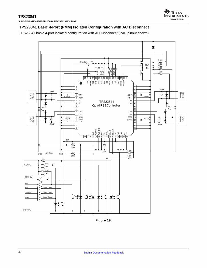
TPS23841 Basic 4-Port (PMM) Isolated Configuration with AC Disconnect
64 62
1
2
3
4
5
6
7
8
9
10
11
12
17 18 19 20
13
14
15
16
21 22 23 24 25 26 27 28 29 30 31 32
61
48
34
33
PO
RB
V10
AG
2
V2.5
RG
Rbia
s
Ct
SY
N
AG
1
V48
P1
N1
RET1
CINT1
P2
N2
RET2CINT
2
P4
N4
CINT4
P3
N3
RET3
CINT3
MS
RET4
V3
DG
SC
L
SD
A_I
SD
A_O
A2
A3
A4
A5
A1
V6.3
ALT
A/B
WD
_D
IS
TPS23841
Quad PSEController
INT
AC
_LO
AC
_H
I
63 60 58 5759 56 54 5355 52 50 4951
47
46
45
44
43
42
41
40
39
38
37
35
36
RJ45-5
Xfo
rmer
0.1
uF
0.1
uF
0.1
uF
124K
220pF
0.027uF
0.027uF
220nF
0.1uF48V BUS
POS NEG
RJ45-5
Xfo
rmer
220nF RJ45-5
Xfo
rmer
RJ45-5
Xfo
rmer
7.5K
7.5K
7.5K
7.5K
68uF
0.027uF
0.027uF
220nF
270
270V
DDCPU
GND CPU
SDA_IN
POR
9.1K
270
SDA_OU
T
INT
SCL
3.9K
3.9K
3.9K
9.1K3.9K
3.9K
0.1
uF
+-
0.5W
0.5W
Open Drain
Open Drain
Open Drain
220nF
AutoFunction
TPS23841SLUS745A–NOVEMBER 2006–REVISED MAY 2007
TPS23841 basic 4-port isolated configuration with AC Disconnect (PAP pinout shown).
Figure 19.
40 Submit Documentation Feedback

TAPE AND REEL INFORMATION
*All dimensions are nominal
Device PackageType
PackageDrawing
Pins SPQ ReelDiameter
(mm)
ReelWidth
W1 (mm)
A0(mm)
B0(mm)
K0(mm)
P1(mm)
W(mm)
Pin1Quadrant
TPS23841PAPR HTQFP PAP 64 1000 330.0 24.4 13.0 13.0 1.5 16.0 24.0 Q2
PACKAGE MATERIALS INFORMATION
www.ti.com 18-Aug-2014
Pack Materials-Page 1
*All dimensions are nominal
Device Package Type Package Drawing Pins SPQ Length (mm) Width (mm) Height (mm)
TPS23841PAPR HTQFP PAP 64 1000 367.0 367.0 45.0
PACKAGE MATERIALS INFORMATION
www.ti.com 18-Aug-2014
Pack Materials-Page 2


IMPORTANT NOTICE
Texas Instruments Incorporated and its subsidiaries (TI) reserve the right to make corrections, enhancements, improvements and otherchanges to its semiconductor products and services per JESD46, latest issue, and to discontinue any product or service per JESD48, latestissue. Buyers should obtain the latest relevant information before placing orders and should verify that such information is current andcomplete. All semiconductor products (also referred to herein as “components”) are sold subject to TI’s terms and conditions of salesupplied at the time of order acknowledgment.TI warrants performance of its components to the specifications applicable at the time of sale, in accordance with the warranty in TI’s termsand conditions of sale of semiconductor products. Testing and other quality control techniques are used to the extent TI deems necessaryto support this warranty. Except where mandated by applicable law, testing of all parameters of each component is not necessarilyperformed.TI assumes no liability for applications assistance or the design of Buyers’ products. Buyers are responsible for their products andapplications using TI components. To minimize the risks associated with Buyers’ products and applications, Buyers should provideadequate design and operating safeguards.TI does not warrant or represent that any license, either express or implied, is granted under any patent right, copyright, mask work right, orother intellectual property right relating to any combination, machine, or process in which TI components or services are used. Informationpublished by TI regarding third-party products or services does not constitute a license to use such products or services or a warranty orendorsement thereof. Use of such information may require a license from a third party under the patents or other intellectual property of thethird party, or a license from TI under the patents or other intellectual property of TI.Reproduction of significant portions of TI information in TI data books or data sheets is permissible only if reproduction is without alterationand is accompanied by all associated warranties, conditions, limitations, and notices. TI is not responsible or liable for such altereddocumentation. Information of third parties may be subject to additional restrictions.Resale of TI components or services with statements different from or beyond the parameters stated by TI for that component or servicevoids all express and any implied warranties for the associated TI component or service and is an unfair and deceptive business practice.TI is not responsible or liable for any such statements.Buyer acknowledges and agrees that it is solely responsible for compliance with all legal, regulatory and safety-related requirementsconcerning its products, and any use of TI components in its applications, notwithstanding any applications-related information or supportthat may be provided by TI. Buyer represents and agrees that it has all the necessary expertise to create and implement safeguards whichanticipate dangerous consequences of failures, monitor failures and their consequences, lessen the likelihood of failures that might causeharm and take appropriate remedial actions. Buyer will fully indemnify TI and its representatives against any damages arising out of the useof any TI components in safety-critical applications.In some cases, TI components may be promoted specifically to facilitate safety-related applications. With such components, TI’s goal is tohelp enable customers to design and create their own end-product solutions that meet applicable functional safety standards andrequirements. Nonetheless, such components are subject to these terms.No TI components are authorized for use in FDA Class III (or similar life-critical medical equipment) unless authorized officers of the partieshave executed a special agreement specifically governing such use.Only those TI components which TI has specifically designated as military grade or “enhanced plastic” are designed and intended for use inmilitary/aerospace applications or environments. Buyer acknowledges and agrees that any military or aerospace use of TI componentswhich have not been so designated is solely at the Buyer's risk, and that Buyer is solely responsible for compliance with all legal andregulatory requirements in connection with such use.TI has specifically designated certain components as meeting ISO/TS16949 requirements, mainly for automotive use. In any case of use ofnon-designated products, TI will not be responsible for any failure to meet ISO/TS16949.
Products ApplicationsAudio www.ti.com/audio Automotive and Transportation www.ti.com/automotiveAmplifiers amplifier.ti.com Communications and Telecom www.ti.com/communicationsData Converters dataconverter.ti.com Computers and Peripherals www.ti.com/computersDLP® Products www.dlp.com Consumer Electronics www.ti.com/consumer-appsDSP dsp.ti.com Energy and Lighting www.ti.com/energyClocks and Timers www.ti.com/clocks Industrial www.ti.com/industrialInterface interface.ti.com Medical www.ti.com/medicalLogic logic.ti.com Security www.ti.com/securityPower Mgmt power.ti.com Space, Avionics and Defense www.ti.com/space-avionics-defenseMicrocontrollers microcontroller.ti.com Video and Imaging www.ti.com/videoRFID www.ti-rfid.comOMAP Applications Processors www.ti.com/omap TI E2E Community e2e.ti.comWireless Connectivity www.ti.com/wirelessconnectivity
Mailing Address: Texas Instruments, Post Office Box 655303, Dallas, Texas 75265Copyright © 2016, Texas Instruments Incorporated