high-performance networking processors for automotive
TRANSCRIPT

Company External – NXP, the NXP logo, and NXP secure connections for a smarter world are trademarks of
NXP B.V. All other product or service names are the property of their respective owners. © 2018 NXP B.V.
Network Systems Engineer
Geoff Waters
High-Performance Networking Processors for Automotive Applications
October 2018 | AMF-AUT-T3168

PUBLIC 11PUBLIC
• Layerscape Product Family
• Network Processing
• ADAS Processing
• Suitability
Agenda

PUBLIC 2
NXP DN (Digital Networking) Business
Digital Networking high
performance networking
and computing processors
offer server class
performance for real time
control and high touch
data services in wireless &
wireline infrastructure
Data/Cloud
Enterprise
Service
Provider
Cloud Edge
Industrial
Intelligent Transportation

PUBLIC 3
DN Processors in Mission Critical Applications
Fuel Management, Main Flight Control, Secondary Flight Control, Aircraft Engine
Management, Cockpit Display
Rocket navigation, Artillery Control Computer, IFF
IFF, UAV Flight Computer, Defense Airborne Computer, Weapon
Navigation System, Ground Control System
Robotics Controllers, Motion Controllers, Multi-Axis Motor Controllers, Safety PLCs
Traction Control, Railway Signaling Controller, Railway Communications, Brake
Controller
Power Distribution Relays, Smart Grid Communications
Aerospace Military and Defense
Factory Automation Railway Power Grid

PUBLIC 4
Multicore for Avionics Working Group F2F
The Multicore for Avionics Working Group conference is a two-day, deep dive into technical training that targets skills development for engineers
across a broad range of embedded technology solutions. In addition to live-demonstrations of the latest innovations from NXP and its partners, the
event offers workshops and lectures over multiple markets allowing attendees to customize a schedule that is most relevant to their training needs.
Objectives
Format2 day eventCities throughout America
20 hours of technical training sessionsFrom NXP and sponsors
General sessions, specialty tracks, sponsor demos,
evening networking event
“Meet the Experts” opportunities
City/State Date
Austin | Texas October 23-24

PUBLIC 5
NXP Auto’s View of Domains and Functions
Bo
dy &
Com
fort
Driver
Exp
erie
nce
Con
ne
ctivity
Dri
ve
r
Rep
lace
me
nt
Po
we
rtra
in &
Ve
hic
le
Dyn
am
ics
SENSE THINK ACT
V2X
Broadcast Radio
Cellular
NFC
Smart Car Access
Radar
Camera
Lidar
Motion & Pressure
Speed
Ultrasonic
Smart Light
Access, Door Ctrl
eCockpit
Amplifiers
Powertrain &
Vehicle DynamicsEngine
Transmission
Brake
Battery Cell Management
Steering
Airbag
Suspension
Infotainment
Fusion
WiFi, BT, GNSS,
TPMS
Powertrain
Domain Controller
Connectivity
Domain Controller
Body
Domain Controller 4
5
1
2
3

PUBLIC 6
Conceptual Vehicle Architecture
Switch
Central Gateway
Actuator
Actuator
Actuator
Actuator
Actuator
Actuator
Actuator
Actuator
Domain
Controller
Sensor
Sensor
Sensor
Sensor
Sensor Processor(Vision)
Switch
Sensor
Sensor
Sensor
Sensor
Sensor Processor (Radar)
Switch DSRC
V2X
Actuator
Actuator
Actuator
Actuator
Domain
Controller
Domain
Controller
Sensor
Sensor
Sensor
Sensor
Sensor Processor(LiDAR)
Switch
Infotainment/
eCockpit
Telematics
Control Unit /
Wireless
Gateway
Cellular
Modem
Wi-Fi
/ BT
CPU
AD Central Fusion
CPU
Massive
Parallel
Acceleratio
n
SafetySafety
Packet Acceleration
C-
V2X
S32V S32P/S S32D
GPS
Security
Ethernet
Router
Layerscape
options

PUBLIC 7
LS1012A• Cortex-A53
• 800MHz
• 2Gbps Packet
• 1Gbps Crypto
• 1-2W
• Lowest power
64-bit ARM
LS1021A• Cortex-A7
• 2 cores
• 1GHz
• 2Gbps Pkt
• 1Gbps Crypto
• 2W
LS1043A• Cortex-A53
• 2-4 cores
• 10Gbps Pkt
• 5Gbps Crypto
• 4-8W
• 1st 64-bit ARM
processor
LS1084A• Cortex-A53
• 4-8 cores
• 1.5GHz
• DPAA2
• 20Gbps Pkt
• 10Gbps Crypto
• 15-20W
• 1st 8x A53 ARM
Next gen
programmable
offload
LS1046A• Cortex-A72
• 4 cores
• DPAA1
• 10Gbps Pkt
• 10Gbps Crypto
• 8-15W
• 1st Value Tier A72
ARM
LS2084A• Cortex-A72
• 4-8 cores
• DPAA2
• 40G Pkt
• 20G Crypto
• 20-35W
• 1st 8x A72 ARM
Next gen
programmable
offload
LX2160A• Cortex-A72
• 16 cores
• 100Gbps Pkt
• 100Gbps Crypto
• 40W
• 1st 16nm product
LS1028A• Cortex-A72
• 2 cores
• 5Gbps Pkt
• 5Gbps Crypto
• 4-9W
• 1st with TSN switch
• Integrated GPU
In Development
Pin Compatible
Auto Qual Plan*
* Additional products can be auto
qualified with business justification
Layerscape Portfolio

PUBLIC 8
NXP ARM Processor Networking & High Speed IO
Ethernet MAC
(capable, not aggregate)PCIe USB
Product 10G 2.5G 1G Controllers Max lanes 2.0 3.0
S32V234 0 1 2 2x 3.0 2 1 0
i.MX 8DualMax 0 0 1 2x 3.0 1 2 1
i.MX 8Quad* 0 0 2 2x 3.0 1 2 1
LS1012A 0 2 2 1x 2.0 2 1 1
LS1043A 1 2 5 3x 2.0 4 0 3
LS1046A 2 2 5 3x 3.0 8 0 3
LS1084A 2 0 8 3x 2.0 8 0 3
LS2084A 8 8 8 3x 3.0 16 0 2
LX2160A 10 10 16 6x 4.0 24 0 2
Refer to product specific documents for exact features and performance

PUBLIC 9
Layerscape for Vehicle Network
Processing

PUBLIC 10
NXP Vehicle Network Processing Module Roadmap
2015 2016 2017
2Q 3Q 4Q1Q2Q 3Q 4Q1Q2Q 3Q 4Q 2Q 3Q 4Q1Q
2018
2Q 3Q 4Q1Q 2Q1Q
2019
High-end ENET
Secure Routing
Gateway
ENET Secure
Gateway /
Domain
Controller
Traditional
CAN/LIN
Gateway / Body
Controller
2020
MPC5748G6MB, 160MHz, 2 x Z4 & 1 x Z2
FlexRay, Ethernet, ISO CAN FD,
USB, SDHC, MLB
MPC5746C3MB, 160MHz, 1 x Z4 & 1 x Z2
FlexRay, Ethernet, ISO CAN FD
MPC5746B2MB, 160MHz, 1 x Z4
FlexRay, Ethernet, ISO CAN FD
ProductionConcept Execution
Real-time (AUTOSAR) MCU
Linux-capable, multicore platform
Subject to change without notice.
3Q 4Q
2021
2Q 3Q 4Q1Q
LS1043A
4x A53, 1.6GHz
MultiGbps Ethernet
MPC5748G6MB, 160MHz, 2 x Z4 & 1 x Z2
FlexRay, Ethernet, ISO CAN FD,
USB, SDHC, MLB
Vehicle Network
Processing Module Vehicle Network
Processing Module Next-Gen
S32 Family SoC
Secure Gateway
MPC5748G-LCEVB

PUBLIC 11
SP
I-to-C
AN
SP
I-to-C
AN
…
Vehicle Network Processing Module Features
CA
N P
HY
Dig
ita
l IN
Dig
ita
l O
UT NAND
(Managed)
32/64-bit
DDR3(L)
Ethernet Switch:
SJA1105/P
SafetyWDOG SBC
MPC5748G(AUTOSAR)
CA
N P
HY
x8CH
TJA1102
OABR PHY
1-L
ane
PC
Ie
…
PMIC
CAN100
BASE-T
OBD
x1CH 1-Port
TJA1102
OABR PHYPHY
LS1043A(Linux/QNX)
Ethernet IPC
8x CAN-FD
Ethernet
PHY + Switch
C6M
Power Reg
LS1043
Power Reg
External Memories
& Expansion
SPI-to-CAN2.0OBD
• Enables Next-gen CAN-Ethernet Gateways
− Automotive Gateway + Network Processing
(Gigabit Ethernet Packet Routing) + Applications
− MPC5748G (MCU) + LS1043A (MPU)
− Available today
• Feature Set
− CAN Signal Gateway (ASIL B)
− 4x Arm Cortex-A53 (LS1043A) for Applications
− Packet Forwarding Engine
• OS Support
− AUTOSAR: Real-time CAN gateway
− Linux / QNX: Ethernet routing, applications processing

PUBLIC 12
Vehicle Network Processing Module Features
VNPM (MPC5748G + LS1043A)
Microcontroller + Microprocessor
Six processor cores:
(2) PowerPC z4 + (1) PowerPC z2
(4) ARM Cortex-A53 @ 1.6 GHz
Up to 20K DMIPS processing
Ethernet Packet Acceleration
768 KB SRAM, 6MB embedded flash, DDR3L/DDR4 support
(2) 10/100 Ethernet (MPC5748G)
(4) Up to 10G Ethernet (LS1043A)
(8) CAN FD / (18) LIN
(1) USB 2.0, (3) USB 3.0, (3) Gen2 PCIe
Security: Secure Boot, HiPerf Crypto, HSM Security
ASIL B functional safety
Production: Now

PUBLIC 13
Vehicle Network Processing Module: Key Functions

PUBLIC 14
Demo ApplicationsDual Chip Module Demo Applications Software

PUBLIC 15
Vehicle Network Processing Demo Apps
Calypso 6M IPC
Ethernet
Packet
Acceleration
Black box – Automotive
Cloud Based Data Logger
& Visualizer
SDN
Intrusion Detection

PUBLIC 16
Network Processing Acceleration
Web based Application in ASK (Application Solution Kit) with below functionalities
Demonstrating packet acceleration during network load
Enabling and disabling of HW acceleration (Slow Path/Fast path with load on primary cores)
Realtime CPU Load monitoring
Router setup/configuration connecting two PCs
PC1
PC2
Note: App GUI shown is for illustration purpose. Actual one may differ.
ASK
VNPM
CalypsoLayerscape
CPU Monitoring
Value
Propositions:
Ethernet
Packet
Acceleration
vs. SW based
competitor

PUBLIC 17
VNPM 1.0
CalypsoLayerscape
Software Defined Networking (SDN) in Vehicular Networks
Full functional SDN Stack showcased on one Arm Cortex-A53 core in Layerscape
A demo app (functionality proposed by DN) demonstrating OpenFlow switch with a Control Agent
Realtime CPU Load monitoring demonstrating three Cores near idle
Core1 Core2
Core 3 Core 4
ASK
IPC
Value Propositions:
Cloud controlled
firewall: Connectivity,
Ethernet, Apps
Processing.

PUBLIC 18
VNPM 1.0
CalypsoLayerscape
Automotive Data Logger
Vehicle Health Parameters recorder - "relevant" data from Vehicle logged into a mass storage.
Calypso receiving the CAN data from an external CAN traffic generator.
Data transmitted via IPC to Layerscape for logging.
Logged Data shared over cloud
Data fetched from cloud for monitoring.
CAN Traffic Generator
Data Logging
Data Cloud
IPCData Visualization
Data shared over Cloud
Value
Propositions:
• Cloud
connectivity
(Apps
Processing)
• PCIe memory
• MCU to MPU
(CAN-Eth)
• Security (CAN,
Eth & Cloud)
PUBLIC 19
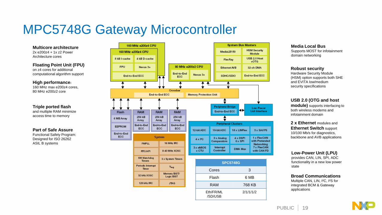
MPC5748G Gateway MicrocontrollerMulticore architecture2x e200z4 + 1x z2 Power
Architecture cores
Floating Point Unit (FPU) on z4 cores for additional
computational algorithm support
High performance:
160 MHz max e200z4 cores,
80 MHz e200z2 core
Media Local Bus Supports MOST for infotainment
domain networking
USB 2.0 (OTG and host
module) supports interfacing to
both wireless modems and
infotainment domain
2 x Ethernet modules and
Ethernet Switch support
10/100 Mb/s for diagnostics,
backbone and AVB applications
Part of Safe Assure Functional Safety Program:
Designed for ISO 26262
ASIL B systems
Low-Power Unit (LPU) provides CAN, LIN, SPI, ADC
functionality in a new low power
state
Broad Communications Multiple CAN, LIN, I²C, I²S for
integrated BCM & Gateway
applications
Triple ported flash and multiple RAM minimize
access time to memory
Robust security Hardware Security Module
(HSM) option supports both SHE
and EVITA low/medium
security specifications
SPC5748G
Cores 3
Flash 6 MB
RAM 768 KB
Eth/FR/ML
/SD/USB
2/1/1/1/2

PUBLIC 20
QorIQ Layerscape LS1043ACE (Grade 3)
Performance• ARM A53 x 4 @ up to 1.6GHz (LS1023A: 2 cores)
– 19.5K DMIPS
– SpecInt2k6 – 5.95, Rate -15
– Neon SIMD in all CPUs
• 1x36b (including ECC) DDR3L/4 up to 1.6GT/s– 6.4GB/s memory BW
• High Speed IO– Multiple PCIe Gen2 controllers
– Multiple Ethernet MACs (up to 10G)
Auto Quality• AEC Q100 Grade 3 (105 Tj)
• 15 years product longevity
• ZD-like approach to reduce risk of DPPM
or Life failures
• Expected Operating Life fail rate <10 FIT
• Mission Profile: 10 years, 90C Tj-effective
Security• 5Gbps Crypto Acceleration
• IPsec, SSL
• Trust Architecture– Secure Boot
– Secure Debug
– Secure Storage
– Tamper Detection
– HW Enforced Partitioning
– ARM Trust Zone
Functional Safety• Target ASIL-B*
• ECC protected memories
• Fault localization, containment and
recovery
• Soft lockstep with determinism
• Excellent support for virtualization,
containerization
Process & Package• 28HPM, ~4-8W Thermal
Max @ 105C
• 23x23mm, Unlidded
FCBGA, .8mm pitch (780
pins)
32-bit
DDR3L/4
Memory Controller
Interconnect
SA
TA
3
Ge
n2
PE
X
Ge
n2
PE
X
Ge
n2
PE
X
Queue Manager
Buffer ManagerSEC – 5G
Secure Boot
Trust Zone
Power Mgt
SD/eMMC
2x DUART, 6x
LPUART
4x I2C
SPI, GPIO, JTAG
3x USB3.0 + PHYSERDES 4 lanes @ up to 10GHz
Frame Manager
1MB Banked L2
ARM
A53
ARM
A53
ARM
A53
ARM
A53
Parse, Classify,Distribute, Autorespond
10/1G
1G 1G
Flash Ctl, QSPI
uQE
SMMU
2.5/1G
1G2.5/1G
1G
Major Milestone Schedule
Engineering Samples Rev 1.1 Completed / October 4, 2016
Networking/Telecom Qualification Completed / January 25, 2017
AECQ100 grade 3 Qual on Rev 1.1 Complete / Sept 12, 2017
PPAP Completion June 2018

PUBLIC 21
QorIQ Layerscape LS1043ABE (Grade 2)
Performance• ARM A53 x 4 @ up to 1.4GHz (LS1023A: 2 cores)
– SpecInt2k6 – 5.2, Rate -13.1– SpecInt2k6 – 5.95, Rate -15
– Neon SIMD in all CPUs
• 1x36b (including ECC) DDR3L/4 up to 1.6GT/s– 6.4GB/s memory BW
• High Speed IO– Multiple PCIe Gen2 controllers
– Multiple Ethernet MACs (up to 2.5G)
Auto Quality• AEC Q100 Grade 2 (125 Tj)
• 15 years product longevity
• ZD-like approach to reduce risk of DPPM
or Life failures
• Expected Operating Life fail rate <10 FIT
• Mission Profile: 10 years, 90C Tj-effective
Security• 5Gbps Crypto Acceleration
• IPsec, SSL
• Trust Architecture– Secure Boot
– Secure Debug
– Secure Storage
– Tamper Detection
– HW Enforced Partitioning
– ARM Trust Zone
Functional Safety• Target ASIL-B*
• ECC protected memories
• Fault localization, containment and
recovery
• Soft lockstep with determinism
• Excellent support for virtualization,
containerization
Process & Package• 28HPM, up to 9W Thermal
Max @ 125C
• 23x23mm, Unlidded
FCBGA, .8mm pitch (780
pins)
32-bit
DDR3L/4
Memory Controller
Interconnect
SA
TA
3
Ge
n2
PE
X
Ge
n2
PE
X
Ge
n2
PE
X
Queue Manager
Buffer ManagerSEC – 5G
Secure Boot
Trust Zone
Power Mgt
SD/eMMC
2x DUART, 6x
LPUART
4x I2C
SPI, GPIO, JTAG
3x USB3.0 + PHYSERDES 4 lanes @ up to 5GHz
Frame Manager
1MB Banked L2
ARM
A53
ARM
A53
ARM
A53
ARM
A53
Parse, Classify,Distribute, Autorespond
10/1G
1G 1G
Flash Ctl, QSPI
uQE
SMMU
2.5/1G
1G2.5/1G
1G
Major Milestone Schedule
Engineering Samples Completed / May 2018
AECQ100 grade 2 Qual On schedule / Oct, 2018
Grade 2 PPAP Completion On schedule / December 2018

PUBLIC 22
LS1043 SERDES Options
Grade 3 Grade 2
Serdes 1
0 1 2 3
SERDES Prot A B C D
0000 unused unused unused unused
1555 XFI PCIe 1 PCIe 2 PCIe 3
2555 SGMII 2.5G PCIe 1 PCIe 2 PCIe 3
4555 QSGMII PCIe 1 PCIe 2 PCIe 3
4558 QSGMII PCIe 1 PCIe 2 SATA
1355 XFI SGMII 1G PCIe 2 PCIe 3
2355 SGMII 2.5G SGMII 1G PCIe 2 PCIe 3
3335 SGMII 1G SGMII 1G SGMII 1G PCIe 3
3355 SGMII 1G SGMII 1G PCIe 2 PCIe 3
3358 SGMII 1G SGMII 1G PCIe 2 SATA
3558 SGMII 1G PCIe 1 PCIe 2 SATA
3555 SGMII 1G PCIe 1 PCIe 2 PCIe 3
7000 PCIe 1
9998 PCIe 1 PCIe 2 PCIe 3 SATA
6058 PCIe 1 PCIe 2 SATA
1455 XFI QSGMII PCIe 2 PCIe 3
2455 SGMII 2.5G QSGMII PCIe 2 PCIe 3
2255 SGMII 2.5G SGMII 2.5G PCIe 2 PCIe 3
3333 SGMII 1G SGMII 1G SGMII 1G SGMII 1G
1460 XFI QSGMII PCIe 3
2460 SGMII 2.5G QSGMII PCIe 3
3460 SGMII 1G QSGMII PCIe 3
3455 SGMII 1G QSGMII PCIe 2 PCIe 3
9960 PCIe 1 PCIe 2 PCIe 3
2233 SGMII 2.5G SGMII 2.5G SGMII 1G SGMII 1G
2533 SGMII 2.5G PCIe 1 SGMII 1G SGMII 1G
LS1043 SERDES (4 lanes)
• Rows with green right edge are
supported on grade 2 version.
• Rows with black right edge are only
supported on grade 3 version.

PUBLIC 23
LS1043 Network Benchmarks

PUBLIC 24
Board LS1043ARDB (Rev 1.1 silicon)
Kernel/User space SMP Linux 4.1.30 64bit LE kernel / 64bit LE user space
Core 4 x ARMv8 A53 cores each running @ 1.6 GHz
Operations frequency Core/platform/DDR/FMan: 1600/400/1600/500
Cache L1 : 32 Kbytes Dcache and Icache
L2 : 1 Mbytes
Memory Single DDR controller with 2GB DDR4 at 1600 MT/s
U-Boot U-boot 2016.09
SEC Sec 5.4(2 DECOs)
FMan Fman v3
rcw RR_FQPP_1455/rcw_1600.bin
2 x RGMII, 4 x QSGMII, 1 x XFI(copper)
Filesystem Ramdisk file system
Compiler gcc-4.9.2, glibc-2.15, binutils-2.23.2
https://www.nxp.com/support/developer-resources/software-development-
tools/qoriq-developer-resources/qoriq-ls1043a-reference-design-
board:LS1043A-RDB?
LS1043ARDB System Description

PUBLIC 25
Autonomous Packet Forwarding
• Fman classifies frame, determines it matches a rule for autonomous forwarding.
• Frame is buffered to main memory during the Rx process (Fman isn’t a switch)
• Fman determines Tx port, reads frame from memory, performs encapsulations/manipulation, transmits
• A53 cores are only involved in new flow set-ups, not in forwarding of flows already in the Fman’s forwarding table
32-bit
DDR3L/4
Memory Controller
Interconnect
US
B
Gen2 P
EX
Gen2 P
EX
Gen2 P
EX
Queue Manager
Buffer ManagerSEC – 5G
Frame Manager
1MB Banked L2
ARM
A53
ARM
A53
ARM
A53
ARM
A53
Parse, Classify,Distribute, Autorespond
10/1G
1G 1G
uQE
SMMU
2.5/1G
1G2.5/1G
1G
DDR

PUBLIC 26
LS1043A Autonomous Ethernet Forwarding(Broadband Router Application Solutions Kit)
Release Interface Protocol Traffic Type Measured Throughput (Gbps)CPU Load
%
ASK 0.7 Ethernet
IPv4/v6 128B Packets with 128 flows 6.2 0.2
IPv4/v6 256B Packets with 128 flows 10.0 0.2
NAPT 128B Packets with 128 flows 5.1 0.2
NAPT 256B Packets with 128 flows 10.0 0.2
L2-Bridging 128B Packets with 128 flows 10.0 0.2
NAT-PT 128B Packets with 128 flows 3.9 0.2
NAT-PT 256B Packets with 128 flows 7.7 0.2
Note: test setup limited to 10Gbps line rate

PUBLIC 27
Apps Processor Packet Forwarding
• Fman classifies frame, determines which A53 software queue it belongs to.
• Frame is buffered to main memory during the Rx process
• A53 software reads the frame from main memory (most likely only the header), determines Tx port, performs
encapsulations/manipulation, writes frame updates back to main memory. Software enqueues frame descriptor to Fman
• Fman reads frame from main memory, transmits
• Fman can perform some in-line offloads, but A53 software required due to the complexity of the classification or
manipulation.
32-bit
DDR3L/4
Memory Controller
Interconnect
US
B
Ge
n2
PE
X
Ge
n2
PE
X
Ge
n2
PE
X
Queue Manager
Buffer ManagerSEC – 5G
Frame Manager
1MB Banked L2
ARM
A53
ARM
A53
ARM
A53
ARM
A53
Parse, Classify,Distribute, Autorespond
10/1G
1G 1G
uQE
SMMU
2.5/1G
1G2.5/1G
1G
DDR

PUBLIC 28
Apps Processor Packet Forwarding
Platform Core#Through
put
Frame Size (bytes)
64 128 256 390 512 1024 1280 1518
LS1043ARDB
(1600/400/1600/
500)
1Kpps 357 361 363 362 363 361 361 360
Mbps 240 427 802 1188 1545 3015 3758 4431
2Kpps 723 731 742 750 750 718 577 488
Mbps 486 866 1639 2459 3190 6000 6000 6000
4Kpps 1690 1686 1673 1649 1410 718 577 488
Mbps 1136 1996 3694 5409 6000 6000 6000 6000
Green color means line rate traffic
Optimized User Space IP Forwarding (USDPAA)
Plain Vanilla Linux IPv4 Forwarding
CoresThrough
put
Frame Size (bytes)
64 128 256 390 512 1024 1280 1518
LS1043ARDB
(1600/400/1600/
500)
1Kpps 3304 3296 3296 2792 2522 1426 1154 975
Mbps 2220 3902 7278 9158 10735 11907 12000 12000
2Kpps 6497 5785 4048 2824 2533 1424 1154 975
Mbps 4366 6849 8937 9262 10782 11896 12000 12000
4Kpps 7222 5785 4048 2820 2528 1421 1154 975
Mbps 4853 6849 8937 9250 10759 11872 12000 12000

PUBLIC 29
Apps Processor Packet Forwarding (Higher Complexity)
Platform Num of cores
L2 frame size (bytes)
82 408 1442
L2 frame size after encryption (bytes)
154 474 1514
Aggregate Plaintext (Kpps)
Aggregate Plaintext (Mbps)
Aggregate Plaintext (Kpps)
Aggregate Plaintext (Mbps)
Aggregate Plaintext (Kpps)
Aggregate Plaintext (Mbps)
LS1043ARDB
(1600/400/1600/500)
1 core 115 94 116 398 110 1300
2 cores 229 187 227 777 214 2505
4 cores 440 359 426 1463 325 3809
Plain Vanilla Linux IPSec Forwarding (Crypto is HW accelerated)
Platform Num of cores
L2 frame size (bytes)
82 408 1442
L2 frame size after encryption (bytes)
154 474 1514
Aggregate
Plaintext (Kpps)
Aggregate Plaintext
(Mbps)
Aggregate Plaintext
(Kpps)
Aggregate Plaintext
(Mbps)
Aggregate Plaintext
(Kpps)
Aggregate Plaintext
(Mbps)
LS1043ARDB
(1600/400/1600/500)
1 core 792 646 758 2598 464 5426
2 cores 1467 1197 1166 3993 465 5437
4 cores 2277 1858 1276 4370 465 5432
Optimized User Space IPsec Forwarding (USDPAA)

PUBLIC 30
Apps Processor Packet Forwarding (Protocol Interworking)
• Modem connected via USB writes frame to an address in main memory. Address is based on descriptor ring
managed by the modem and the modem’s driver running on the A53s. Modem driver will determine whether
software polls or is notified of new frame via interrupt.
• A53 software reads the frame from main memory (most likely only the header), determines Tx port, performs
encapsulations/manipulation, writes frame updates back to main memory. Software enqueues frame
descriptor to Fman
• Fman reads frame from main memory, transmits
32-bit
DDR3L/4
Memory Controller
Interconnect
US
B
Gen2 P
EX
Gen2 P
EX
Gen2 P
EX
Queue Manager
Buffer ManagerSEC – 5G
Frame Manager
1MB Banked L2
ARM
A53
ARM
A53
ARM
A53
ARM
A53
Parse, Classify,Distribute, Autorespond
10/1G
1G 1G
uQE
SMMU
2.5/1G
1G2.5/1G
1G
DDR
Modem
PUBLIC 31
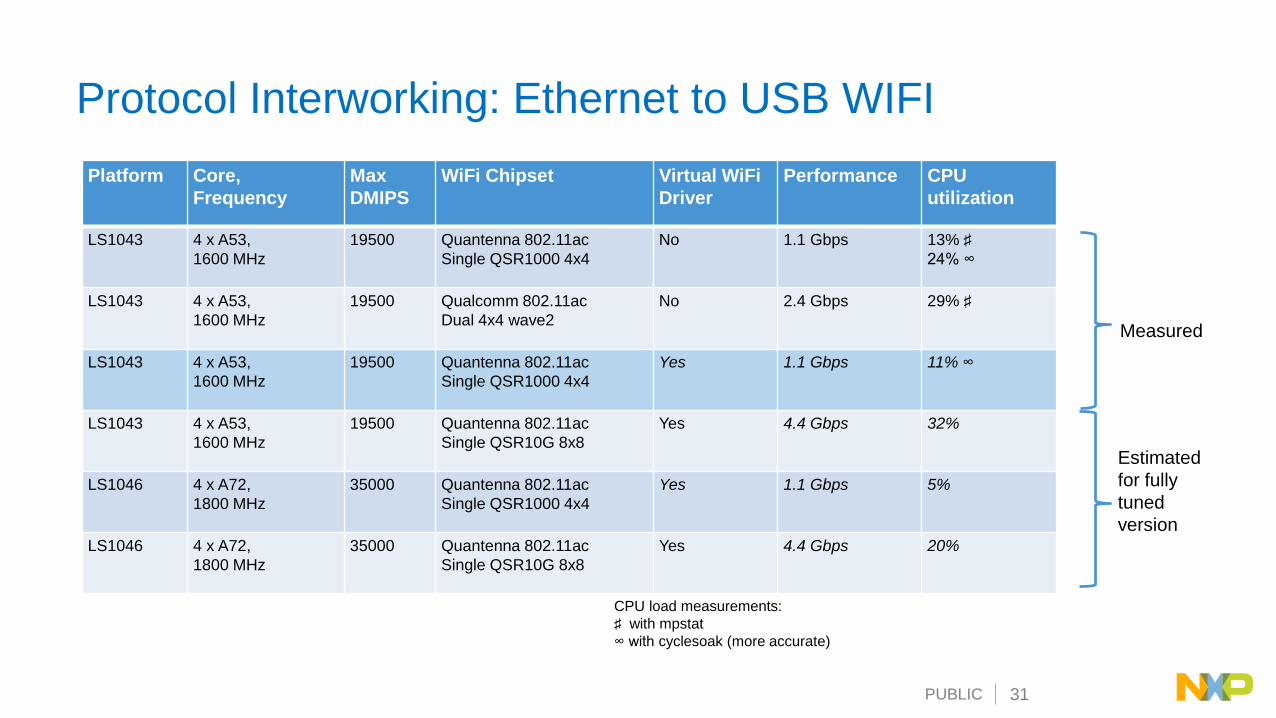
Protocol Interworking: Ethernet to USB WIFI
Platform Core,
Frequency
Max
DMIPS
WiFi Chipset Virtual WiFi
Driver
Performance CPU
utilization
LS1043 4 x A53,
1600 MHz
19500 Quantenna 802.11ac
Single QSR1000 4x4
No 1.1 Gbps 13% ♯
24% ∞
LS1043 4 x A53,
1600 MHz
19500 Qualcomm 802.11ac
Dual 4x4 wave2
No 2.4 Gbps 29% ♯
LS1043 4 x A53,
1600 MHz
19500 Quantenna 802.11ac
Single QSR1000 4x4
Yes 1.1 Gbps 11% ∞
LS1043 4 x A53,
1600 MHz
19500 Quantenna 802.11ac
Single QSR10G 8x8
Yes 4.4 Gbps 32%
LS1046 4 x A72,
1800 MHz
35000 Quantenna 802.11ac
Single QSR1000 4x4
Yes 1.1 Gbps 5%
LS1046 4 x A72,
1800 MHz
35000 Quantenna 802.11ac
Single QSR10G 8x8
Yes 4.4 Gbps 20%
CPU load measurements:
♯ with mpstat
∞ with cyclesoak (more accurate)
Estimated
for fully
tuned
version
Measured

PUBLIC 32
Vehicle Server/Gateway Scalability
Eth
ern
et
PC
Ie
Au
to IF
s
S32 S32
Apps Proc
S32 S32 S32
1x 1
0G
2x 2
.5G
3x P
CIe
4x 1
G
LS1043A
2x 1
0G
1x 2
.5G
3x P
CIe
4x 1
GLS1046A
8x 1
0G
8x 1
/2.5
G
4x P
CIe
LS2084A
8x 1
0G
8x 1
/2.5
G
6x P
CIe
LX2160
Calypso
2x 2
.5G
4x 1
G
LS1043A
Au
to IF
s
Calypso
Au
to IF
s
2x 1
0G
1x 2
.5G
3x P
CIe
4x 1
G
LS1046A
1x 1
0G
Calypso
1x 2
.5G
4x 1
G T
SN
LS1028
Au
to IF
s
Eth
ern
et
PC
Ie
Au
to IF
s
Eth
ern
et
PC
Ie
Au
to IF
s
Eth
ern
et
PC
Ie
Au
to IF
s
Eth
ern
et
PC
Ie
Au
to IF
s
3x P
CIe
2x P
CIe
Pin
compatible

PUBLIC 33
QorIQ Layerscape LS1046AStatus: In Production (Networking/Telecom)
Full Auto qual: If requested, ~6mos after MOU
Auto Production: Immediately upon qual completion
Performance• ARM A72 x 4 @ 1.8 GHz
– 42.9K DMIPS
– SpecInt2k6 – 13.3, Rate -37.4
– Neon SIMD in all CPUs
• 1x36/72b (including ECC) DDR4 up to 2.1GT/s
– 16.8GB/s memory BW
• High Speed IO
– Multiple PCIe Gen3 controllers
– Multiple Ethernet MACs (up to 10G)
Auto quality
• AEC Q100 Grade 3 (105 Tj) - achievable, qual plan with MOU
• 15 years product longevity
• ZD-like approach to reduce risk of DPPM or Life failures
• Expected Operating Life fail rate <10 FIT
• Mission Profile: 10 years, 90C Tj-effective
Security• 10Gbps Crypto Acceleration
• IPsec, SSL
• Trust Architecture– Secure Boot
– Secure Debug
– Secure Storage
– Tamper Detection
– HW Enforced Partitioning
– ARM Trust Zone
Functional Safety• Target ASIL-B*
• ECC protected memories
• Fault localization, containment and recovery
• Soft lockstep with determinism
• Excellent support for virtualization, containerization
Process & Package• 28HPM, ~8-15W Thermal Max @ 105C
• 23x23mm, Lidded FCBGA, .8mm pitch (780 pins)
36/72-bit DDR4
Memory Controller
Interconnect
SA
TA
3
Ge
n3
PE
X
Ge
n3
PE
X
Ge
n3
PE
X
Queue Manager
Buffer ManagerSEC – 10G
Secure Boot
Trust Zone
Power Mgt
2x SD/eMMC
4x UART
4x I2C
SPI, GPIO, JTAG
3x USB3.0 + PHYSERDES 8 lanes @ up to 10GHz
Frame Manager
2MB Banked L2
ARM
A72
ARM
A72
ARM
A72
ARM
A72
Parse, Classify,Distribute, Autorespond
1G 1G10G
10G
1G 1G2.5G
Flash Ctl, QSPI
PUBLIC 34
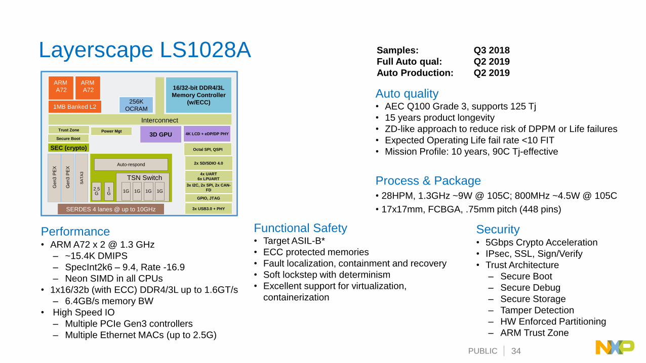
Layerscape LS1028A Samples: Q3 2018
Full Auto qual: Q2 2019
Auto Production: Q2 2019
Performance• ARM A72 x 2 @ 1.3 GHz
– ~15.4K DMIPS
– SpecInt2k6 – 9.4, Rate -16.9
– Neon SIMD in all CPUs
• 1x16/32b (with ECC) DDR4/3L up to 1.6GT/s
– 6.4GB/s memory BW
• High Speed IO
– Multiple PCIe Gen3 controllers
– Multiple Ethernet MACs (up to 2.5G)
Auto quality• AEC Q100 Grade 3, supports 125 Tj
• 15 years product longevity
• ZD-like approach to reduce risk of DPPM or Life failures
• Expected Operating Life fail rate <10 FIT
• Mission Profile: 10 years, 90C Tj-effective
Security• 5Gbps Crypto Acceleration
• IPsec, SSL, Sign/Verify
• Trust Architecture
– Secure Boot
– Secure Debug
– Secure Storage
– Tamper Detection
– HW Enforced Partitioning
– ARM Trust Zone
Functional Safety• Target ASIL-B*
• ECC protected memories
• Fault localization, containment and recovery
• Soft lockstep with determinism
• Excellent support for virtualization,
containerization
Process & Package• 28HPM, 1.3GHz ~9W @ 105C; 800MHz ~4.5W @ 105C
• 17x17mm, FCBGA, .75mm pitch (448 pins)
16/32-bit DDR4/3L
Memory Controller
(w/ECC)
Interconnect
SA
TA
3
Gen3 P
EX
Gen3 P
EX
SEC (crypto)
Secure Boot
Trust Zone Power Mgt
2x SD/SDIO 4.0
4x UART
6x LPUART
3x USB3.0 + PHYSERDES 4 lanes @ up to 10GHz
1MB Banked L2
ARM
A72
ARM
A72
Auto-respond
2.5G
1G
Octal SPI, QSPI
256K
OCRAM
3x I2C, 2x SPI, 2x CAN-
FD
GPIO, JTAG
1G 1G 1G 1G
TSN Switch
4K LCD + eDP/DP PHY3D GPU
PUBLIC 35
Layerscape for ADAS

PUBLIC 36
Level 2/3 Autonomy Market
Introduction

PUBLIC 37
ADAS and Driving Functions
L0
L3
L4
L1
L2
Highway Driving up to 140km/h with
construction sites
Cruising Chauffeur
Highway Driving <60-80 kmh No
const sites
Driver initiated lane changed
Automated Lane change
Automated Valet parking
Traffic Jam Chauffeur
Traffic Jam assist
Lane keep/change
assist
Intersection assist (steer &
brake)
Overtaking Assist (steer and acc)
ACC with Steering
Lane centring & keeping
Cross traffic (break only)
Rear collision mitigation
Aut. parallel parking (steer
only)
ACC
(braking only)
Lane Changing Assist
EBAStability control
Cross traffic alert
Navigation
Blind spot monitoring
Ped/Cycl
detection
Parking aid
Traffic sign recognition
Lane departure warning
Forward collision warning
Surroundrear view
Brake control
Steering control
Propulsion control
Radar CamerasDriver
monitoringLidar
Ultrasonic sensors
Interior sensors
GPSHDMAPS
(Cloud)V2X
Aut. Brake City/Urban/VRUs
Free Drive
L5
Robo Taxi
Aut. Shuttle
Driving Functions drives the real Value of Automated Driving
Sensor
Actuator
Autonomy
Level

PUBLIC 38
The Race to Self-Driving As Per the SAE Classification
ADAS
Responsibility for safe operation Control of complete vehicle Control of steering Control of vehicle speed
Self-Driving
LEVEL 1
Driver Assistance
LEVEL 2
Partial Automation
LEVEL 3
Conditional Automation
• Adaptive cruise control
• Automatic braking
• Lane keeping
• Partial automated parking
• Traffic jam assistance
• Emergency brake with steer
• Semi autonomous:
− Highway chauffeur
− Self parking
• Human driver can regain
control
Driver
Vehicle or
Driver
Vehicle
Driver
Vehicle
LEVEL 4
High Automation
• Autonomous driving in
some driving modes
• Human driver may not
respond to request to
intervene
Driver
Vehicle
LEVEL 5
Full Automation
• Fully autonomous under all
driving modes
• Human driver not expected
to respond to request to
intervene
Driver
Vehicle
NXP Automated Drive Kit Focus

PUBLIC 39
NXP Offerings for L2/3 Vehicles

PUBLIC 40
• Histogram/Particle Filters
• Kalman Filters
• Deep Learning (ex: CNNs)
• Optimal Routing
• Collision Avoidance
• Control Algorithms
• Plausibility Analysis and Recovery
Localization & Object Detection
Motion Planning
Control Laws
Functional Safety
Massive Parallel Acceleration
Single threaded control,
Sequential
Multi-Tasking(x86, ARMv8)
Lockstep
Checkpoint, Voting
(GPGPU, VSPA, APEX…)
High Autonomous Vehicle Computing Types

PUBLIC 41
Central Fusion Architectures
Level 2/3 Level 3-5
Sensor Sensor
Sensor Sensor
Sensor Sensor
Sensor Sensor
Sensor Sensor
Sensor Sensor
Brain/Central Fusion
Segmentation
C
Level 2-5
Safety
Companion
Sensor Sensor
Sensor Sensor
Sensor
Domain
Processor
Segmentation
Sensor Sensor
Sensor Sensor
Sensor
Domain
Processor
Segmentation
Sensor Sensor
Sensor Sensor
Sensor
Domain
Processor
Segmentation
Brain/Central Fusion
B
Classification
Perception
Classification
Sensor Fusion
Feature Fusion
Behavioral Modelling
Motion Control
Sensor Sensor
Sensor Sensor
Sensor
Domain
Processor
Segmentation
Central Fusion +
Sensor Domain
Processor
Segmentation
Sensor Sensor
Sensor Sensor
A
Perception
Classification
Sensor Fusion
Feature Fusion
Behavioral Modelling
Motion Control
Safety
Companion
Perception
Classification
Sensor Fusion
Feature Fusion
Behavioral Modelling
Motion Control
Segmentation Segmentation
Functional Apps
Functional Apps
Functional Apps

PUBLIC 42
Switch
Data Conversion
Gateway
CPU
Central Fusion Unit
SafetyCPU
Switch
Big Brain
CPU Accelerator
Big Brain
Switch
Data Conversion
Gateway/Little Brain
CPU
Central Fusion Unit
SafetyCPU
Switch
Big Brain
CPU Accelerator
Little Brain
or
Redundant Brains
Accelerator
Accelerator

PUBLIC 43
SoCs + Basic Software
BlueBox Hardware Reference
Designs & Linux SDK
NXP
NXP
AutonomouStuff Autonomous Drive Kit,
built on BlueBox
hardware
OfferingsWhose product?

PUBLIC 44

PUBLIC 45
Custom Case Styles
• In-vehicle tests may require
custom cases for the BlueBox 2
PCB
• Custom case designs are
possible
−NXP provides a sheet metal
enclosure

PUBLIC 46
Why the BlueBox?
• NXP BlueBox: A development platform for Automated Drive and
Sensor Fusion applications, with functional safety, vision acceleration
and automotive interfaces
• PC to Embedded: Deploy PC developed algorithms to an embedded
target suitable for deployment in test vehicles
• Expansion: BlueBox 2.0, baseline configuration suited to L3 use
cases with expansion capability to support higher autonomy level use
cases/applications
PUBLIC 47
What’s Provided When You Order a BlueBox 2.0 from NXP?Power
• Power supply (100-240V, 50-60Hz AC to 12V 16A DC)
− Provided with Universal power adapter
• Separate wire-end external power cable for connection to batteries, etc
Front and Rear I/O supplies (incl. storage)
• UART Cable: 3x RS232 to single 10-pin header for front port serial access to S32V, S32R and LS2
• RS232-to-USB multiport adapter
• Rear Auto Ethernet: Auto-breakout cable (34-pin to twisted wire-end)
• Rear CAN/FlexRay/Power Controls: Auto-breakout cable (26-pin to twisted wire-end)
• Front panel HDMI (from S32V): 1x HDMI to Mini HDMI cable
• 2x Cat 6 ethernet cables
• SFP+ optical transceiver module + optical patch cord (2 meters long)
• 16GB MicroSD card (boot and mass storage for S32V234)
• LiteOn Automotive SSD, 256GB SATA 2.5 Inch (internal, connected to LS2 SATA, preprogrammed with Linux root file system)
• Maxim GMSL to MIPI CSI-2 Deserializer card (Internal, adds maxim compatible coax camera inputs on rear panel)
Debug
• JTAG adapter board for 20pin to 10pin debug (Needed for low level S32V, LS2 debug)
− Cable for JTAG adapter board (from 10pin on adapter board to 10pin on BlueBox board)
• Cable for CPLD programming (Controls LS2 start-up, usually not necessary)

PUBLIC 48
Where is the BlueBox Being Used?
Baidu Apollo: ported on BB2.0, Road
simulation on-going, gathering dataAutonomouStuff: Highway Pilot full
system based on BlueBox2.0 ready
to be distributed by AS
Truck Platooning: system safety
concept validation, live testing of
CPU load depending on driving
functions, fixed point acceleration
analysis

PUBLIC 49
Automated Drive Kit
from AutonomouStuff

PUBLIC 50
NXP Automated Drive Kit – AutonomouStuff
AutonomouStuff:
• Value added reseller
• Accelerates development by building automated research platforms
• Prepares, maintains, supports and re-sells the NXP Automated Drive Kit
• Offers perception positioning software based on NXP Automated Drive Kit
• System integration and ROS enablement for sensors and other hardware plus reference applications
• First line system support

PUBLIC 51
Research Vehicle Platform Example – AutonomouStuff

PUBLIC 52
What is the NXP Automated Drive Kit (Release 1)?
The Phase 1 kit will contain the following:
• Computing: NXP BlueBox 2.0, BLBX2-DB
• Vision: Neusoft Front Camera SW running on S32V234 (inside BLBX2-DB) with Truly MIPI CSI2 Camera
• LiDAR: Selection of Lidars supported
• Long Range Front Facing RADAR
• IMU & Integrated GPS
• O/S: Auto SDK Linux + Ubuntu RFS + VethSW
• Middleware: ROS (Robot Operating System)

PUBLIC 53
Autonomous Drive Kit Software Architecture
BlueBox 2.0 Hardware Platform
LS2084A
AutonomouStuff ARMv8-based sensor fusion nodes
SMP Linux +
Ubuntu root file system +
HAL support packages
ROS Kinetic
USB
Ethern
et P0
Ethern
et P2
Ethern
et P3
PCIe Host
S32VPCIe End Point seen
as a network interface
Single
Camera
MIPI
Virtual Ethernet
Interface (PCIe0)
Ubuntu Linux
User-Space
Ubuntu Linux kernel-space
MIPI
Driver
AutonomouStuff
ADAS software
ROS Kinetic
Neusoft ARMv8-based camera nodeVirtual Ethernet
Interface (PCIe0)
NovaTel
ProPak
6
USB
Hub
Kvaser USB
to CAN
Drive by
wire
RADAR
3rd Party ADAS APIs accessed
by AutonomouStuff nodes for
lane and vehicle detection
ROS multi-machine messaging is
used to share camera node
results
vEthernet provides
standard API

PUBLIC 54
Summary – NXP Automated Drive Kit
• Full System [HW + SW] Development Platform with pathway to production silicon solutions!− Easily move from PC environment to NXP Automated Drive Kit to test vehicle with
minimal effort
− Allows customer resources to focus on value added software
• Address levels of autonomy up to Level 3− Flexible set of ADAS sensors to fit customer requirements
• NXP Automated Drive Kit purchased through AutonomouStuff− https://autonomoustuff.com/product/nxp-automated-drive-kit/

PUBLIC 55
BB 1.0
• ASIL B
• 72K DMIPS
• Autosar
• Vision Processing
BB 2.0
• ASIL D
• 90K DMIPS
• Autosar
• Vision interfaces
• Vision Processing
• Expandability (add’l PCIe slot)
BB 3.0
• ASIL D
• 160K DMIPS
• Autosar
• Vision interfaces
• Vision Processing
LS2084A
S32V234
LS2084A
S32V234
S32R274
LX2160A
S32V3
Now
Q1 17
Q4 18
Q2 17
BlueBox Roadmap

PUBLIC 56
Layerscape LS2084A
Performance• ARM A72 x 8 @ 2.0 GHz
• 95.3K DMIPS
• SpecInt2k6 – 14.5, Rate -83.4
• Neon SIMD in all CPUs
• 2x72b (including ECC) DDR4 up to 2.1GT/s
• 33.6GB/s memory BW
• High Speed IO
• Multiple PCIe Gen3 controllers
• Multiple Ethernet MACs (up to 10G)
Auto Quality
• AEC Q100 Grade 3 (105C Tj)
• 15 years product longevity
• ZD-like approach to reduce risk of DPPM or Life failures
• Expected Operating Life fail rate <10 FIT
• Mission Profile: 10 years, 90C Tj-effective
Security• 20Gbps Crypto Acceleration
• MACSEC, IPsec, SSL
• Trust Architecture
• Secure Boot
• Secure Debug
• Secure Storage
• Tamper Detection
• HW Enforced Partitioning
• ARM Trust Zone
Functional Safety• Target ASIL-B*
• ECC protected memories
• Fault localization, containment and recovery
• Soft lockstep with determinism
• Excellent support for virtualization, containerization
Process & Package
• 28HPM, ~40W Thermal Max @ 105C
• 37.5 x 37.5 mm, lidded FCBGA, 1mm pitch, 1292 pins
72
-bit D
DR
4
Me
mo
ry
Co
ntr
olle
r
1 M
B
Pla
tform
Cache
1MB Banked L2
ARM
A72
ARM
A72
Interconnect
72
-bit D
DR
4
Me
mo
ry
Co
ntr
olle
r
SA
TA
3S
AT
A3
x8 G
en3 P
EX
x4 G
en3 P
EX
x4 G
en3 P
EX
x8 G
en3 P
EX
Queue Manager
Buffer Manager
SEC – 20G
DCE – 20G
Secure Boot
Trust Zone
Power Mgt
SD/eMMC
2x DUART
4x I2C
SPI, GPIO, JTAG
2x USB3.0 + PHY
SERDES 16 lanes @ up to 10GHz
Wire Rate IO Processor
2MB Packet Buffer
8x1/10 + 8x1 Ethernet MACs
L2 Switching
1MB Banked L2
ARM
A72
ARM
A72
1MB Banked L2
ARM
A72
ARM
A72
1MB Banked L2
ARM
A72
ARM
A72
PME – 10G
Major Milestone Schedule
Samples (Production Rev) Dec 2017
Networking/Telecom Qualification March 2018
AECQ100 grade 3 Qual on production rev Nov 2018
PPAP Completion Dec 2018

PUBLIC 57
Layerscape LX2160A72-b
it D
DR
4
Me
mo
ry
Co
ntr
oll
er
4 M
B
Pla
tfo
rm
Ca
ch
e
Samples: March 2018
Full Auto qual: Q1 2020
Production: Q1 2020
Performance
• ARM A72 x 16 @ 2.2 GHz
– ~210K DMIPS
– SpecInt2k6 – 16, Rate -183
– Neon SIMD in all CPUs
• 2x72b (including ECC) DDR4 up to 3.2GT/s
– 51GB/s memory BW
• High Speed IO
• Multiple PCIe Gen4 controllers
• Multiple Ethernet MACs (up to 100G)
Auto quality
• AEC Q100 Grade 3 (105 Tj)
• 15 years product longevity
• ZD-like approach to reduce risk of
DPPM or Life failures
• Expected Operating Life fail rate <10
FIT
• Mission Profile: 10 years, 90C Tj-
effective
Security
• 50Gbps Crypto Acceleration
• MACSEC, IPsec, SSL
• Trust Architecture
– Secure Boot
– Secure Debug
– Secure Storage
– Tamper Detection
– HW Enforced Partitioning
– ARM Trust Zone
Functional Safety
• Target ASIL-B*
• ECC protected memories
• Fault localization, containment and recovery
• Soft lockstep with determinism
• Excellent support for virtualization, containerization
2MB Banked L2
ARM
A72
ARM
A72
ARM
A72
ARM
A72
2MB Banked L2
ARM
A72
ARM
A72
ARM
A72
ARM
A72
Interconnect
72-b
it D
DR
4
Me
mo
ry
Co
ntr
oll
er
SA
TA
3S
AT
A3
x8
Ge
n4
PE
Xx4
Ge
n4
PE
Xx4
Ge
n4
PE
X
x8
Ge
n4
PE
X
x4
Ge
n4
PE
X
x4
Ge
n4
PE
X
SA
TA
3S
AT
A3
Queue Manager
Buffer Manager
SEC – 50G
DCE – 50G
Secure Boot
Trust Zone
Power Mgt
SD/eMMC
2x DUART4x I2C / 2x CAN-
FDSPI, GPIO, JTAG
2x USB3.0 + PHY
Wire Rate IO Processor
2MB Packet Buffer
SERDES 24 lanes @ up to 25GHz
10/25/40/50/100 Ethernet MACs
L2 Switching
Process & Package• 16nm FinFET Compact, ~40W Thermal Max @ 105C
• 40x40mm, Lidded FCBGA, 1mm pitch (1517 pins)
2MB Banked L2
ARM
A72
ARM
A72
ARM
A72
ARM
A72
2MB Banked L2
ARM
A72
ARM
A72
ARM
A72
ARM
A72

PUBLIC 58
LX2 Family Portrait
LX2080A
LX2120A
Interconnect
WRIOP
2MB PEB
8MB Platform Cache
IO MMU IO MMUIO MMU
24 lanes @ up to 25GHz
72-bit
DDR4
with
ECC
72-bit
DDR4
with
ECC
A72
A72
IO MMU
1MB L2
QB-
Man
SEC – 50G
DCE – 100G
130Gbps 1/ 2.5 / 10 / 25 / 40 / 50 /
100 Ethernet
SA
TA
3S
AT
A3
x8 G
en4 P
CIe
x4 G
en4 P
CIe
x4 G
en4 P
CIe
x8 G
en4 P
CIe
x4 G
en4 P
CIe
x4 G
en4 P
CIe
SA
TA
3S
AT
A3
Secure Boot
Trust Zone
Power Management
SD/eMMC
2x DUART
6x I2C
SPI, GPIO, JTAG
2x USB3.0 + PHY
2x CAN-FD
A72
A72
1MB L2
A72
A72
1MB L2
A72
A72
1MB L2
A72
A72
1MB L2
A72
A72
1MB L2
A72
A72
1MB L2
A72
A72
1MB L2
LX2160A

PUBLIC 59
LX2 Schedule
Milestone Date
Product Launch October 2017
Tapeout February 2018
Alpha samples May 2018
SDK EAR June 2018
Beta Samples June 2018
Reference Design Boards (RDBs) available for purchase August 2018
Rev 2.0 Tapeout Feb 2019
Production Candidate Samples June 2019
Production Tested Units Aug 2019
Networking/Telecom Qualification Nov. 2019
Auto AECQ100 grade 3 Qualification Feb. 2020

PUBLIC 60
LX2160 SerDes Table – Choose Each Bank Independently
SERDES1 (x8)
0 1 2 3 4 5 6 7
H G F E D C B A
1 PCIe.1 x4 PCIe.2 x4
2 SGMII.3 SGMII.4 SGMII.5 SGMII.6 PCIe.2 x4
3USXGMII /
XFI.3
USXGMII /
XFI.4
USXGMII /
XFI.5
USXGMII /
XFI.6PCIe.2 x4
4 SGMII.3 SGMII.4 SGMII.5 SGMII.6 SGMII.7 SGMII.8 SGMII.9 SGMII.10
5 PCIe.1 x4USXGMII /
XFI.7
USXGMII /
XFI.8
USXGMII /
XFI.9
USXGMII /
XFI.10
6USXGMII /
XFI.3
USXGMII /
XFI.4SGMII.5 SGMII.6 SGMII.7 SGMII.8 SGMII.9 SGMII.10
7USXGMII /
XFI.3
USXGMII /
XFI.4
USXGMII /
XFI.5
USXGMII /
XFI.6SGMII.7 SGMII.8 SGMII.9 SGMII.10
8USXGMII /
XFI.3
USXGMII /
XFI.4
USXGMII /
XFI.5
USXGMII /
XFI.6
USXGMII /
XFI.7
USXGMII /
XFI.8
USXGMII /
XFI.9
USXGMII /
XFI.10
9 PCIe.1 x1 SGMII.4 SGMII.5 SGMII.6 PCIe.2 x1 SGMII.8 SGMII.9 SGMII.10
10PCIe.1 x1
(gen 1,2)
USXGMII /
XFI.4
USXGMII /
XFI.5
USXGMII /
XFI.6
PCIe.2 x1
(gen 1,2)
USXGMII /
XFI.8
USXGMII /
XFI.9
USXGMII /
XFI.10
11 PCIe.1 x2 SGMII.5 SGMII.6 PCIe.2 x2 SGMII.9 SGMII.10
12 PCIe.1 x4 PCIe.2 x2 SGMII.9 SGMII.10
13 100GE.1 100GE.2
14 100GE.1 PCIe.2 x4
15 50GE.1 50GE.2 PCIe.2 x4
16 50GE.1 25GE.5 25GE.6 PCIe.2 x4
17 25GE.3 25GE.4 25GE.5 25GE.6 PCIe.2 x4
18USXGMII /
XFI.3
USXGMII /
XFI.425GE.5 25GE.6
USXGMII /
XFI.7
USXGMII /
XFI.8
USXGMII /
XFI.9
USXGMII /
XFI.10
19USXGMII /
XFI.3
USXGMII /
XFI.425GE.5 25GE.6 40GE.2
20 40GE.1 40GE.2
21 25GE.3 25GE.4 25GE.5 25GE.6 PCIe.2 x2 25GE.9 25GE.10
22USXGMII /
XFI.3USXGMII /
XFI.4USXGMII /
XFI.5USXGMII /
XFI.6PCIe.2 x2
USXGMII / XFI.9
USXGMII / XFI.10
SERDES2 (X8)
0 1 2 3 4 5 6 7
A b C D E F G H
1PCIE.3 X2 (GEN1,
GEN2)SATA.1 SATA.2 PCIe.4 x4 (gen 1,2)
2 PCIE.3 X8
3 PCIE.3 X4 PCIe.4 x4
4 PCIE.3 X4 (GEN 1,2) PCIe.4 x2 (gen 1,2) SATA.1 SATA.2
5 PCIE.3 X4 SATA.3 SATA.4 SATA.1 SATA.2
6 PCIE.3 X4 (GEN 1,2) SGMII.15 SGMII.16USXGMII /
XFI.13
USXGMII /
XFI.14
7PCIe.3 x1
(gen1, 2)sgmii.12 SGMII.17 SGMII.18
PCIe.4 x1
(gen 1,2)SGMII.16
USXGMII /
XFI.13
USXGMI /
XFI.14
8 X x SATA.1 SATA.2 SATA.3 SATA.4USXGMII /
XFI.13
USXGMII /
XFI.14
9 SGMII.11 sgmii.12 SGMII.17 SGMII.18 SGMII.15 SGMII.16 SGMII.13 SGMII.14
10 SGMII.11 sgmii.12 SGMII.17 SGMII.18 PCIe.4 x4
11 PCIe.3 x1 sgmii.12 SGMII.17 SGMII.18 PCIe.4 x1 SGMII.16 SGMII.13 SGMII.14
12 SGMII.11 sgmii.12 SGMII.17 SGMII.18 PCIe.4 x2 (gen 1,2) SATA1 SATA2
13 PCIE.3 X4 PCIe.4 x2 SGMII.13 SGMII.14
14 PCIE.3 X2 SGMII.17 SGMII.18 PCIe.4 x2 SGMII.13 SGMII.14
SERDES3 (x8)
0 1 2 3 4 5 6 7
A B C D E F G H
2 PCIe.5 x8
3 PCIe.5 x4 PCIe.6 x4
PUBLIC 61
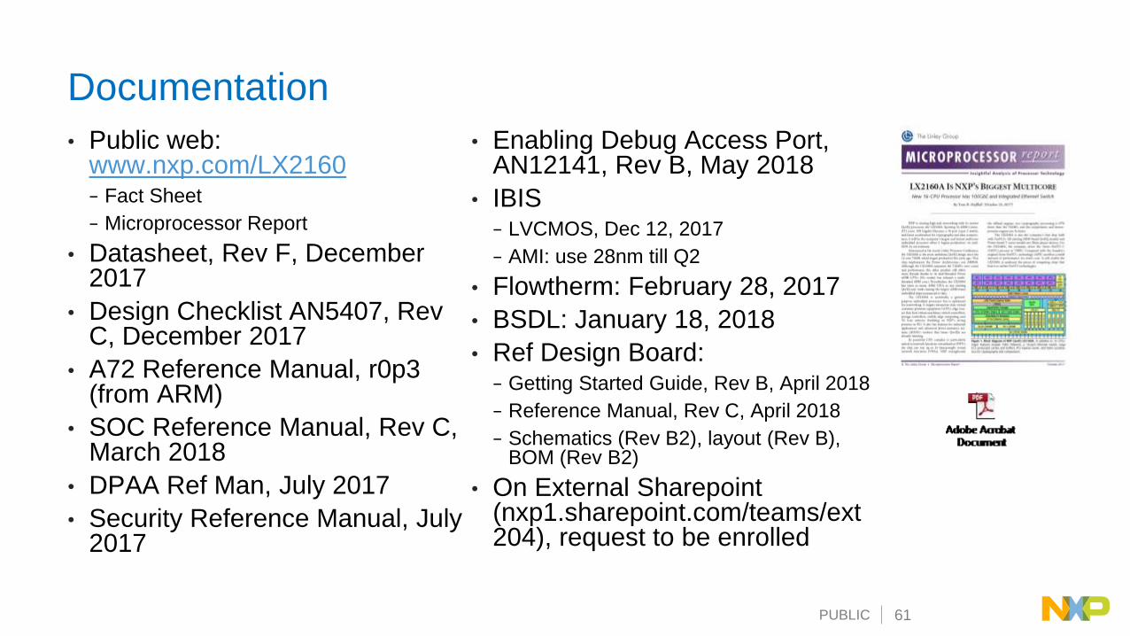
Documentation
• Public web: www.nxp.com/LX2160− Fact Sheet
− Microprocessor Report
• Datasheet, Rev F, December 2017
• Design Checklist AN5407, Rev C, December 2017
• A72 Reference Manual, r0p3 (from ARM)
• SOC Reference Manual, Rev C, March 2018
• DPAA Ref Man, July 2017
• Security Reference Manual, July 2017
• Enabling Debug Access Port, AN12141, Rev B, May 2018
• IBIS − LVCMOS, Dec 12, 2017
− AMI: use 28nm till Q2
• Flowtherm: February 28, 2017
• BSDL: January 18, 2018
• Ref Design Board:− Getting Started Guide, Rev B, April 2018
− Reference Manual, Rev C, April 2018
− Schematics (Rev B2), layout (Rev B), BOM (Rev B2)
• On External Sharepoint(nxp1.sharepoint.com/teams/ext204), request to be enrolled

PUBLIC 62
Other Important Stuff

PUBLIC 63
Layerscape Longevity
NXP Application Processors
• 10 and 15 year supply longevity options
• Formal program with products listed at
www.nxp.com/productlongevity
Industrial & Automotive applications
require product longevity
• Long product lifecycles
• Special product certification required
Digital Networking is still selling the (Motorola) 68302, a processor which was introduced in 1989. Many other products are
still shipping after >20 years.
Any Layerscape product selected for a production vehicle will be guaranteed 10yrs supply, regardless of official start date of
10-15 year guarantee in longevity program.

PUBLIC 64
Layerscape Mission Profiles
Standard Networking Mission Profile
• DN has certified the 28nm technology for 187k
power-on hours with an average of 105C Tj.
• Digital Networking’s standard qualification is for 87k
power-on hours, with an average of ~90C Tj.
Standard Automotive Mission Profile • NXP’s generic automotive mission profile has less power-on hours and a lower average temperature.
• Networking mission profile at 105c/5% Time on Temperature (3/7 completion) equates to 125c/1% Time on Temperature Automotive profile.
• Layerscape products can qualify and meet both profiles.
• Any potential differences the customer has can be evaluated.
Calculated Ta max-eff: 69C
Calculated Tj max-eff: 83C
Calculated Ta max-eff: 71C
Calculated Tj max-eff: 91C

PUBLIC 65
Layerscape Reliability Data
• NXP Digital Networking uses ZD-like approach to reduce risk of DPPM or Life failures.
− DN total product portfolio <0.6PPM.
− 28nm Process Technology Driver (T4240) has customer return rate of 0PPM
− T4240 has demonstrated operating life to 20 years.
• LS2 passed all Industrial Qualification requirements.
− Mission Profile: 10 years, 85C Tj-effective
− Operating Life: 10 year lifetime 28HPM failure rate of 13 FIT, 60% CL
− Early life: PPM 130 PPM, 60% Confidence level
• 28nm Layerscape devices expected to have Operating Life fail rate <10 FIT
− Mission Profile: 10 years, 90C Tj-effective

PUBLIC 66
Layerscape Safety Positioning
• Layerscape SoCs were not designed specifically for the automotive market
and do not offer certain features such as a Fault Collection and Control
Unit (FCCU) that are normally provided in NXP purpose-built automotive
products. However, Layerscape SoCs contain numerous reliability and
security functions that can be leveraged as safety mechanisms.
• Also, careful systems engineering at the board, software, and system level
can compensate for some of the missing automotive-specific hardware
features. Using this sort of holistic design approach, the high performance
computing and network switching capabilities of Layerscape SoCs can be
leveraged in a manner consistent with ISO 26262 ASIL B requirements.

PUBLIC 67
Metric Permanent Transient Combination of
Permanent and
Transient
Single-Point Fault
Metric (SPFM)
89.73% 99.63% 99.60%
Latent Fault Metric
(LFM)
95.14% 99.52% 99.50%
Probablistic Metric
of Hardware
Failure (PMHF)
11.85 FITs 132.97 FITs 144.83 FITs*
• In range for permanent failures…based on multiple system level requirements
• Transient will require close cooperation with the system customer
Layerscape Functional Safety Analysis (LS2)
Meets ASIL-B
Meets ASIL-A

PUBLIC 68
Layerscape in Automotive
• Highest CPU and IO performance SoCs in NXP
• Scalability – 1-16 ARM core SoCs
• Quality & Longevity – Best quality available in high
performance processing. Many devices already on 15
year longevity program.
• Safety – We’ve demonstrated safety for mil/aero and
other critical infrastructure applications. Working to prove
ASIL-B equivalence with auto-centric collateral (FMEDA,
Safety Manual).
• Security – Secure Boot, Secure Debug, Hardware
Enforced Partitioning & Virtualization
• Software – SDKs with a very PC-like look & feel. Broad
support in Linux, history of working with WindRiver, GHS,
and QNX.

PUBLIC 69
Questions

NXP, the NXP logo, and NXP secure connections for a smarter world are trademarks of NXP B.V. All other product or service names are the property of their respective owners. © 2018 NXP B.V.
www.nxp.com