high performance high-k + metal gate strain enhanced
TRANSCRIPT

IEDM 2008
High Performance High-K + Metal Gate Strain Enhanced Transistors on
(110) Silicon
Paul Packan, S. Cea*, H. Deshpande, T. Ghani, M. Giles*, O. Golonzka, M. Hattendorf, R. Kotlyar*, K. Kuhn, A. Murthy, P. Ranade, L. Shifren*,
C. Weber* and K. Zawadzki
Logic Technology Development, *Process Technology Modeling
Intel Corporation

IEDM 2008 2
Outline
Transistor Scaling
Stress Effects on Mobility
Comparison of (100) and (110) Silicon Substrates
Device Performance
Summary

IEDM 2008 3
Key Messages
Record PMOS drive current of 1.2mA/um is presented for devices on (110) silicon substrates
For short gate lengths, NMOS drive currents on (110) substrates are not degraded as much as believed by many in literature
The fundamental physics behind these behaviors is understood

IEDM 2008 4
Outline
Transistor Scaling
Stress Effects on Mobility
Comparison of (100) and (110) Silicon Substrates
Device Performance
Summary

IEDM 2008 5
Traditional Scaling
Traditional device scaling requires all dimensions to scale to maintain performance and leakage
Scaling junction depths and S/D areas is causing Rext
increase
0.0
0.05
0.10
0.15
0.20
0.25
90
100
110
120
130
140
0 50 100 150 200 250Junction Depth (nm)
REXT
Gate Length
REXT
Lmet
@ 1
nA
/um
Ioff
0.0
0.05
0.10
0.15
0.20
0.25
90
100
110
120
130
140
0 50 100 150 200 250Junction Depth (nm)
REXT
Gate Length
REXT
Lmet
@ 1
nA
/um
Ioff
DrainSource
Gate
DrainSourceGate
DrainSource
Gate
DrainSourceGate
Voltage Potential Contours
Id=Cox/Le(Vg-Vt)

IEDM 2008 6
Constant Leakage Scaling
Junction scaling is slowing due to unacceptable resistance increases
Scaling gate lengths at constant leakage requires increasing Vt which results in drive current reduction
Traditional device scaling is losing steam
Id=Cox/Le(Vg-Vt)
0.20.30.40.50.60.70.80.9
11.1
0.015 0.025 0.035 0.045 0.055
Gate Length
Nor
mal
ized
Val
ue IDLIN
IDSAT
VT0.0E+00
5.0E+19
1.0E+20
1.5E+20
2.0E+20
2.5E+20
1992 1994 1996 1998 2000 2002 2004
Year
Dop
ing
Con
cent
ratio
n
0
200
400
600
800
1000
1200
1400
Junc
tion
Dep
th
DepthDoping
Solid Solubility

IEDM 2008 7
Mobility Scaling
Increasing mobility increases device performance without increasing leakage
Reducing scattering mechanisms, applying stress and surface orientation all affect mobility
15
25
35
90nm 65nm 45nmTechnology node
Ge
Con
c. (%
)
0
10
20
30
40
Gat
e-to
-SiG
e S/
D (n
m) 65 nm
45 nm
Id=Cox/Le(Vg-Vt)

IEDM 2008 8
Outline
Transistor Scaling
Stress Effects on Mobility
Comparison of (100) and (110) Silicon Substrates
Device Performance
Summary
IEDM 2008 9
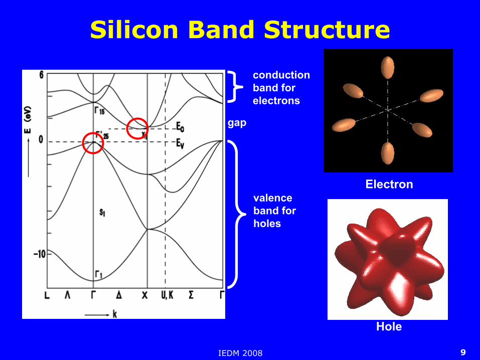
Silicon Band Structure
gap
conductionband forelectrons
valenceband forholes
Electron
hhhh
Hole
IEDM 2008 10
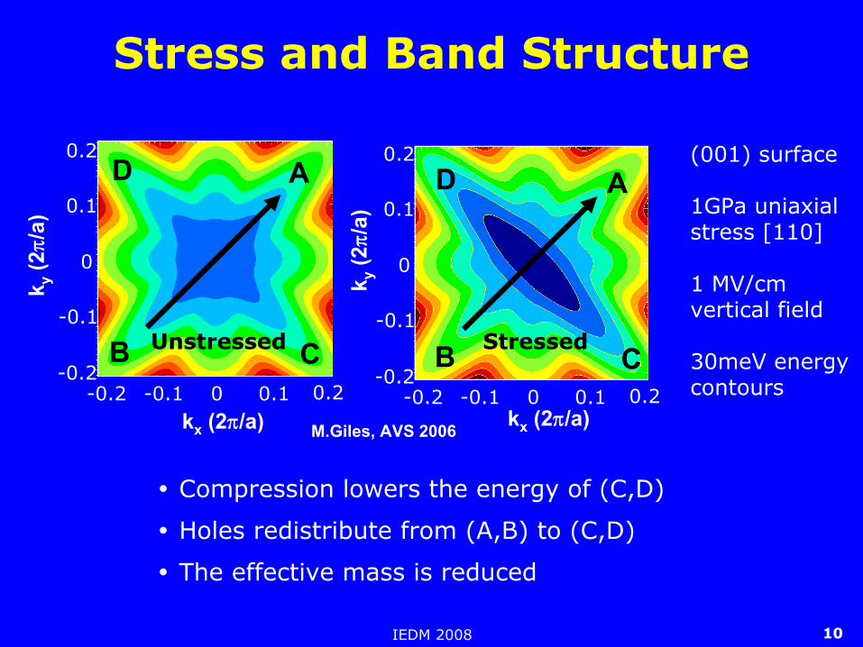
Stress and Band Structure
Compression lowers the energy of (C,D)
Holes redistribute from (A,B) to (C,D)
The effective mass is reduced
M.Giles, AVS 2006
(001) surface
1GPa uniaxial
stress [110]
1 MV/cm vertical field
30meV energy contours
CB
D A
kx
(2/a)
k y(2/
a)
0.2
0.1
0
-0.1
-0.20.20.10-0.1-0.2
C
D
B
kx
(2/a)
k y(2/
a)
A0.2
0.1
0
-0.1
-0.20.20.10-0.1-0.2
Unstressed Stressed
IEDM 2008 11
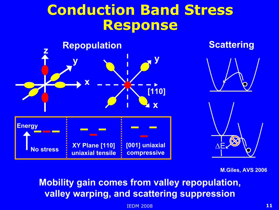
Conduction Band Stress Response
z
x
y
Mobility gain comes from valley repopulation, valley warping, and scattering suppression
[110]
x
y
No stress XY Plane [110]uniaxial tensile
Energy
[001] uniaxialcompressive
E
Repopulation Scattering
M.Giles, AVS 2006

IEDM 2008 12
Stress Effects on Mobility
Longitudinal tension and vertical compression increases electron
mobility
Longitudinal compression and vertical tension increases hole mobility
Transverse tension increases both electron and hole mobility
Hole mobility shows a greater sensitivity to stress for (100)
0.0
1.0
2.0
3.0
4.0
5.0
6.0
-3000 -1000 1000 3000Stress MPa
longitudinal stresstransverse stressvertical stress
0.0
0.5
1.0
1.5
2.0
2.5
-3000 -1000 1000 3000Stress MPa
Mob
ility
Rat
iolongitudinal stress
transverse stress
vertical stress
Electrons Holes0.0
1.0
2.0
3.0
4.0
5.0
6.0
-3000 -1000 1000 3000Stress MPa
longitudinal stresstransverse stressvertical stress
0.0
0.5
1.0
1.5
2.0
2.5
-3000 -1000 1000 3000Stress MPa
Mob
ility
Rat
iolongitudinal stress
transverse stress
vertical stress
Electrons Holes
1 1 MV/cm
1 1 MV/cm
IEDM 2008 13
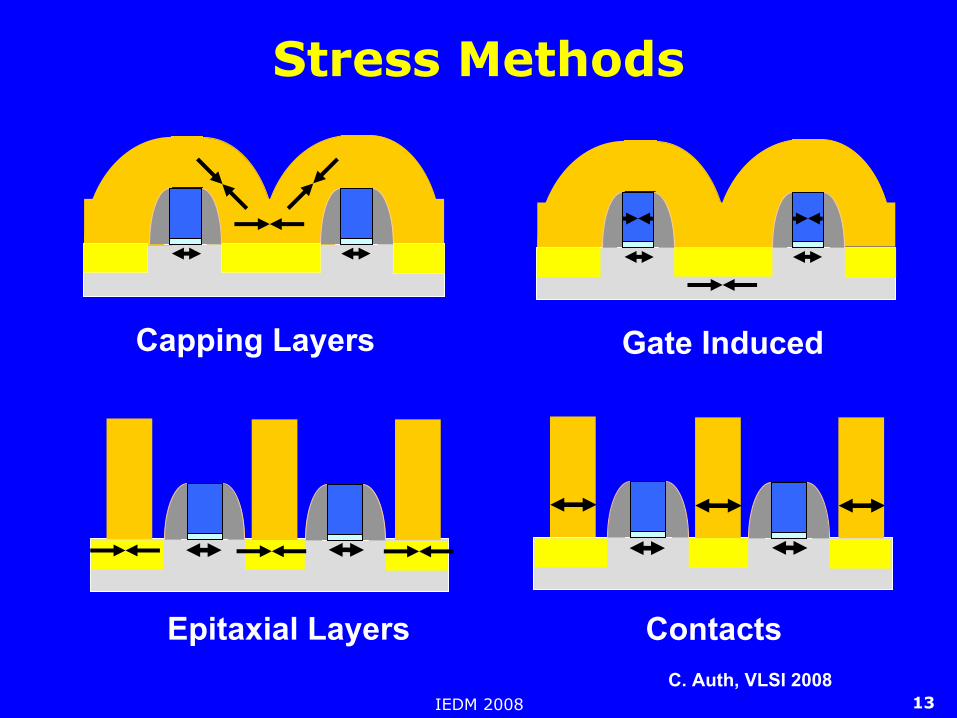
Capping Layers Gate Induced
Contacts
Stress Methods
Epitaxial LayersC. Auth, VLSI 2008
IEDM 2008 14
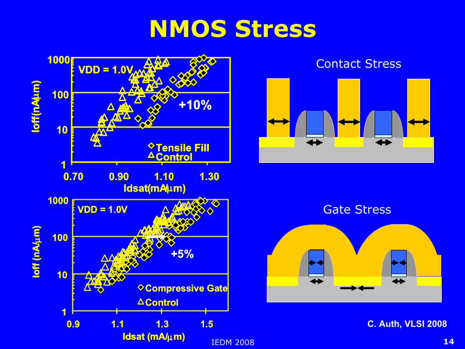
NMOS Stress
C. Auth, VLSI 2008
+10%
1
10
100
1000
0.70 0.90 1.10 1.30Idsat(mA/m)
Ioff
( nA/ m
)
Tensile FillControl
VDD = 1.0V
+10%
1
10
100
1000
0.70 0.90 1.10 1.30Idsat(mA/m)Idsat(mA/m)
Ioff
(nA / m
)Io
ff(n
A / m
)
Tensile FillControlTensile FillControl
VDD = 1.0V
+5%
1
10
100
1000
0.9 1.1 1.3 1.5Idsat (mA/m)
Ioff
(nA
/ m
)
Compressive GateControl
VDD = 1.0V
+5%
1
10
100
1000
0.9 1.1 1.3 1.5Idsat (mA/m)Idsat (mA/m)
Ioff
(nA
/ m
) Io
ff(n
A/
m)
Compressive GateControl
VDD = 1.0V
Contact Stress
Gate Stress

IEDM 2008 15
K.Mistry, 2004 VLSIK.Mistry, 2004 VLSI
PMOS Stress
SiGe Stress

IEDM 2008 16
Outline
Transistor Scaling
Stress Effects on Mobility
Comparison of (100) and (110) Silicon Substrates
Device Performance
Summary

IEDM 2008 17
Substrate Orientation
(100) (110)
calculated
using MASTAR
(http://www.itrs.net/models.html)
[010] [001]
[100]
[010] [001]
[100]

IEDM 2008 18
PMOS Hole Occupation and Band Structure
More dense contour lines show lower effective mass for (110)
PMOS hole occupation of band structure shows a larger difference between unstressed and stressed devices for (100)
kx <110>
ky<-
110>
kx <110>ky
<001
>
(100) (110)
kx <110>
ky<-
110>
kx <110>
ky<-
110>
kx <110>ky
<001
>kx <110>
ky<0
01>
(100) (110)
constant energycontours
stressedunstressed

IEDM 2008 19
Stress Response of Electron Mobility
Longitudinal tension improves (100) and (110) mobility
Vertical and transverse stress show opposite dependencies
Stress sensitivity is larger for (110) substrate orientation
0.0
1.0
2.0
3.0
4.0
5.0
6.0
-3000 -1000 1000 3000Stress MPa
longitudinal stresstransverse stressvertical stress
0.0
0.5
1.0
1.5
2.0
2.5
-3000 -1000 1000 3000Stress MPa
Mob
ility
Rat
io
longitudinal stress
transverse stress
vertical stress
Electrons Holes0.0
1.0
2.0
3.0
4.0
5.0
6.0
-3000 -1000 1000 3000Stress MPa
longitudinal stresstransverse stressvertical stress
0.0
0.5
1.0
1.5
2.0
2.5
-3000 -1000 1000 3000Stress MPa
Mob
ility
Rat
io
longitudinal stress
transverse stress
vertical stress
Electrons Holes(100)
(100)
Mob
ility
Rat
io
0.0
0.5
1.0
1.5
2.0
2.5
3.0
3.5
4.0
-3000 -1000 1000 3000Stress MPa
longitudinal stresstransverse stressvertical stress
Electrons
Mob
ility
Rat
io
0.0
0.5
1.0
1.5
2.0
2.5
3.0
3.5
4.0
-3000 -1000 1000 3000Stress MPa
longitudinal stresstransverse stressvertical stress
Electrons(110)
longitudinal stresstransverse stressvertical stress
longitudinal stresstransverse stressvertical stress
Stress MPa Stress MPa
longitudinal stresstransverse stressvertical stress
longitudinal stresstransverse stressvertical stress
IEDM 2008 20
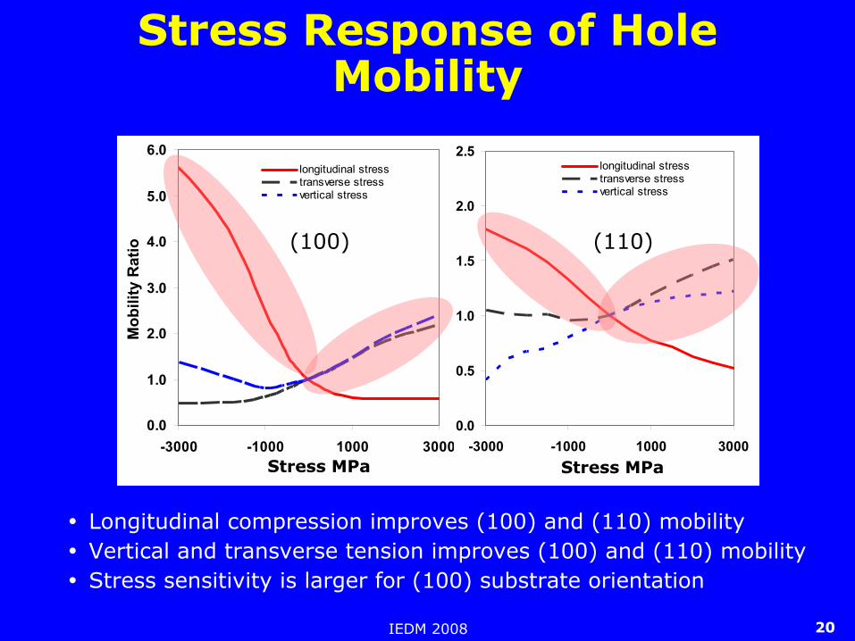
Stress Response of Hole Mobility
0.0
0.5
1.0
1.5
2.0
2.5
-3000 -1000 1000 3000Stress MPa
Mob
ility
Rat
io
longitudinal stresstransverse stressvertical stress
Holes0.0
0.5
1.0
1.5
2.0
2.5
3.0
3.5
4.0
-3000 -1000 1000 3000Stress MPa
Mob
ility
Rat
io
longitudinal stresstransverse stressvertical stress
Electrons0.0
0.5
1.0
1.5
2.0
2.5
-3000 -1000 1000 3000Stress MPa
Mob
ility
Rat
io
longitudinal stresstransverse stressvertical stress
Holes0.0
0.5
1.0
1.5
2.0
2.5
3.0
3.5
4.0
-3000 -1000 1000 3000Stress MPa
Mob
ility
Rat
io
longitudinal stresstransverse stressvertical stress
Electrons0.0
1.0
2.0
3.0
4.0
5.0
6.0
-3000 -1000 1000 3000Stress MPa
longitudinal stresstransverse stressvertical stress
Holes0.0
1.0
2.0
3.0
4.0
5.0
6.0
-3000 -1000 1000 3000Stress MPa
longitudinal stresstransverse stressvertical stress
Holes
(100) (110)
longitudinal stresstransverse stressvertical stress
longitudinal stresstransverse stressvertical stress
Stress MPa Stress MPa
Longitudinal compression improves (100) and (110) mobility
Vertical and transverse tension improves (100) and (110) mobility
Stress sensitivity is larger for (100) substrate orientation
IEDM 2008 21
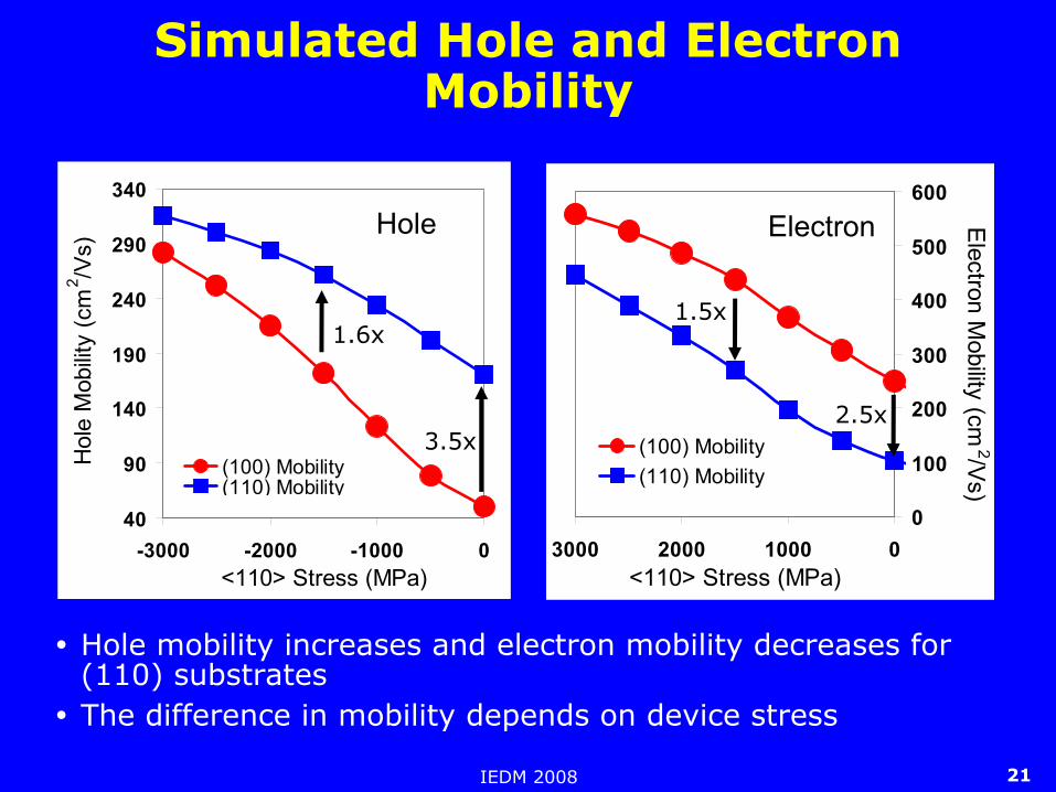
Simulated Hole and Electron Mobility
Hole mobility increases and electron mobility decreases for (110) substrates
The difference in mobility depends on device stress
40
90
140
190
240
290
340
-3000 -2000 -1000 0<110> Stress (MPa)
Hol
e M
obilit
y (c
m2 /V
s)
(100) Mobility(110) Mobility
0
100
200
300
400
500
600
0100020003000<110> Stress (MPa)
Electron M
obility (cm2/V
s)
(100) Mobility(110) Mobility
ElectronHole
3.5x
1.6x
2.5x
1.5x

IEDM 2008 22
Outline
Transistor Scaling
Stress Effects on Mobility
Comparison of (100) and (110) Silicon Substrates
Device Performance
Summary

IEDM 2008 23
45 nm Hi-K+Metal
Gate Technology
Based on Intel’s 45 nm process technology
High-k first, metal gate last process architecture
35nm gate length
160 nm contacted gate pitch
1.0 nm EOT High-k
Dual workfunction
metal gate electrodes
3RD
generation strained silicon
K.Mistry
IEDM 2007

IEDM 2008 24
(110) and (100) PMOS Idsat
Record PMOS drive currents of 1.2 mA/um at 1.0V and 100nA/um Ioff are reported for (110) substrates
The performance improvement is 15% for (110) substrates compared to (100) substrates
1E-9
1E-8
1E-7
1E-6
1E-5
0.7 0.9 1.1 1.3|IDSAT| (mA/um)
IOFF
(A/u
m)
(110)(100)
Ioff
(A
/u
m)
Idsat (mA/um)
15%
1.2

IEDM 2008 25
PMOS (110)/(100) Idsat Improvement versus Stress
Under stress, the relative hole mobility between (110) and (100) substrates decreases due to the larger stress sensitivity of mobility on the (100) substrate
Even under high stress, substantial performance improvement is seen
PMOS
0%
10%
20%
30%
40%
50%
0% 10% 20% 30% 40%Ge Fraction
% ID
SAT
impr
ovem
ent
(110)/(100)
0%
10%
20%
30%
40%
50%
0% 10% 20% 30% 40%Ge Fraction
% ID
SAT
impr
ovem
ent
(110)/(100)experimental data

IEDM 2008 26
(110) and (100) NMOS Idsat
As channel lengths are decreased, NMOS performance loss on (110) substrates is reduced
Why is the degradation reduced?
1E-9
1E-8
1E-7
1E-6
1E-5
0.8 1 1.2 1.4 1.6|IDSAT| (mA/um)
IOFF
(A/u
m)
(110)(100)
1E-5
Ioff
(A
/u
m)
Idsat (mA/um)
1E-6
1E-7
1E-8
1E-9
35nm Lgate
0.2 0.4 0.6IDSAT (mA/um)
(110)(100)
1E-7
1E-8
1E-9
1E-10
1E-11
Ioff
(A
/u
m)
Idsat (mA/um)
160nm Lgate
40%13%

IEDM 2008 27
Surface Confinement Effect
[110] [110]
(100) surface confinement
Ground state
(110) surface confinement
m[110]
=0.19mem[110]
=0.55me
[110]m[110]
=0.43me
Bulk conduction
Surface confinement changes ground state transport mass
Separation depends on confinement field
IEDM 2008 28
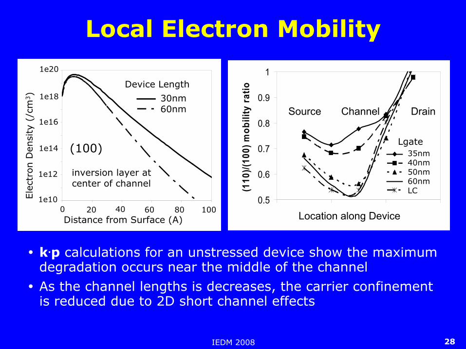
Local Electron Mobility
k.p
calculations for an unstressed device show the maximum degradation occurs near the middle of the channel
As the channel lengths is decreases, the carrier confinement is reduced due to 2D short channel effects
0.5
0.6
0.7
0.8
0.9
1
Slice Location along the Lgate
(110
)/(10
0) m
obili
ty ra
tio
0.0360.040.050.06LC
source tip/channel drain
tip/channel
mid- channel
(a)
Location along Device
Source Channel Drain0.03 um0.06 um
1e20
1e18
1e16
1e14
1e12
1e100 20 40 60 80 100
Ele
ctro
n D
ensi
ty (
/cm
3)
Distance from Surface (A)
Device Length
30nm60nm
35nm40nm50nm60nmLC
Lgate
inversion layer atcenter of channel
(100)

IEDM 2008 29
2D Effects on Valley Splitting
Reduced carrier confinement in short channel devices due to 2D effects reduce the valley splitting
This reduction results in reduced NMOS performance loss for (110) substrates
Valley splitting due to Confinement
field in Long Channel
Eo E1
E2
E1-E2 =large
Valley splitting reduced in Short
Channel
Eo E1
E2 E1-E2 =reduced due to 2D short-channel effects
Valley Splitting due to ConfinementField for Long Channel Device
Valley Splitting Reduction due to2D SCE for Short Channel Device

IEDM 2008 30
Simulated 2D Effects
Simulated NMOS and PMOS performance both with and without 2D effects
The NMOS devices shows a large reduction in short channel degradation when 2D effects are included
Due to high stress effects in the PMOS device, little change is seen by including the 2D effects.

IEDM 2008 31
Narrow Width Stress Effects
STI causes compressive transverse stress in the channel which increases at narrower device widths
Transverse compression improves (110) and degrades (100) electron mobility
NMOS performance for typical devices is only degraded by 5-8%
STI
Channel
GateExpand
Compress
-14%
-12%
-10%
-8%
-6%
-4%
-2%
0%
0 0.25 0.5 0.75 1Device Width (um)
% ID
SAT
Loss
(110)/(100)
-14%
-12%
-10%
-8%
-6%
-4%
-2%
0%
0 0.25 0.5 0.75 1Device Width (um)
% ID
SAT
Loss
(110)/(100)NMOS
IEDM 2008 32
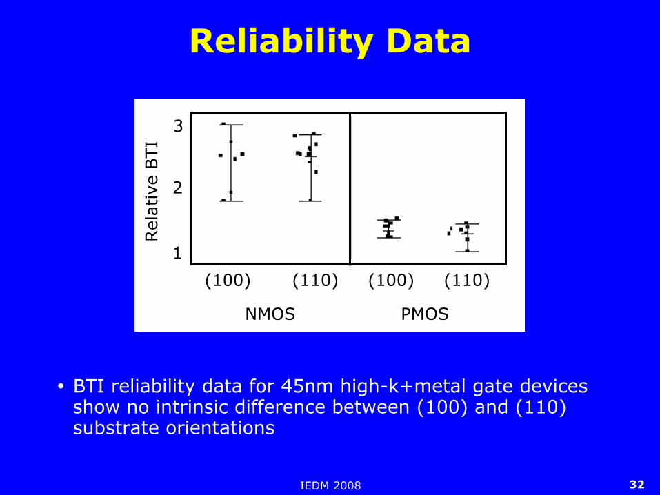
Reliability Data
BTI reliability data for 45nm high-k+metal
gate devices show no intrinsic difference between (100) and (110) substrate orientations
3
2
1
(100) (110) (100) (110)
NMOS PMOS
Rel
ativ
e BTI
IEDM 2008 33
Outline
Transistor Scaling
Stress Effects on Mobility
Comparison of (100) and (110) Silicon Substrates
Device Performance
Summary

IEDM 2008 34
Summary
Record PMOS drive current of 1.2mA/um are shown
PMOS drive currents on (110) substrates show a 15% performance improvement
NMOS drive currents on (110) substrates for typical device widths are only degraded 5-8%
The fundamental physical reason behind these behaviors is understood
The use of (110) silicon substrates is a promising technology option

IEDM 2008 35
For further information on Intel's silicon technology, please visit our Technology & Research page at
www.intel.com/technology