high performance computer systems 300 series …
TRANSCRIPT

HIGH PERFORMANCE COMPUTER SYSTEMS
300 SERIES
SERVICE MANUAL
COMPONENT LEVEL SUPPLEMENT
Part Number 0476,145 Issue 1October 1988

Service Manual Supplement Archimedes 300 series
© Copyright Acorn Computers Limited 1988
Neither the whole nor any part of the information contained in, or the product described in, this manual may be adapted or reproduced in any material form except with the prior written approval of Acorn Computers Limited (Acorn Computers).
The product described in this manual and products for use with it are subject to continuous development and improvement. All information of a technical nature and particulars of the product and its use (including the information and particulars in this manual) are given by Acorn Computers in good faith. However, it is acknowledged that there may be errors or omissions in this manual or in the products it describes. Acorn Computers welcome comments and suggestions relating to the product and this manual. A list of details of any amendments or revisions to this manual can be obtained upon request from Acorn Computers Technical Enquiries or via the Acorn Support Information Database (SID)*.
All correspondence should be adressed to:-
Technical Enquiries
Acorn Computers Limited Fulbourn RoadCherry HintonCambridge CB1 4JN
All maintenance and service on the product must be carried out by Acorn Computers' authorised dealers. Acorn Computers can accept no liability whatsoever for any loss or damage caused by service, maintenance or repair by unauthorised personnel. This manual is intended only to assit the reader in the use of this product, and therefore Acorn Computers shall not be liable for any loss or damage whatsoever arising from the use of any information or particulars in, or any error or omission in, this manual, or any incorrect use of the product.
This manual is for the sole use of Acorn Computers' authorised dealers and must only be used by them in connection with the product described within.
Within this publication the term 'BBC' is used as an abbreviation for 'British Broadcasting Corporation'. Acorn,
Archimedes, ARM and Econet are trademarks of Acorn Computers Limited.
First published 1988
Published by Acorn Computers Limited
Produced by DAW Publications, Cambridge
Part No. 0476,145
*SID is a direct dial viewdata system available to registered SID users. You can gain access to SID on (0223) 243642, this will allow you to inspect the system and use a response frame for registration.

Contents1. Introduction 5.....................................................................................................................................
1.1.Nature and purpose of this manual 5...........................................................................................
2. System Description 6.........................................................................................................................
3. Upgrades 25........................................................................................................................................
4. Fault-finding information 28..............................................................................................................
4.1 Basic Checks 29..........................................................................................................................
4.2 Run Main PCB Functional Test 32.............................................................................................
4.3 Main PCB Faults 32....................................................................................................................
4.3.1 Video failure 32..................................................................................................................
4.3.2 System Failure 32................................................................................................................
4.3.3 Unstable or scrolling display 33..........................................................................................
4.3.4 Corrupted Display 33..........................................................................................................
4.3.5 Colours incorrect or missing 33..........................................................................................
4.4 Peripheral Area Faults 34............................................................................................................
4.4.1 Keyboard and Mouse 34.....................................................................................................
4.4.2 Floppy Disc Drive 34..........................................................................................................
4.4.3 Printer 34.............................................................................................................................
4.4.4 Serial Port 34.......................................................................................................................
4.4.5 Audio 34..............................................................................................................................
4.4.6 Configuration, Non-volatile RAM and Real Time Clock 34..............................................
4.5 Hard Disc 35................................................................................................................................
4.6 Podules 35...................................................................................................................................
4.7 Keyboard 35................................................................................................................................
4.8 Audio 35......................................................................................................................................
4.9 Test ROMs 35.............................................................................................................................
4.9.1 Main Memory Test 36......................................................................................................
4.9.2 Repetitive Reset Test 37.......................................................................................................
5. Appendices 39....................................................................................................................................
5.1 Parts Lists 41..............................................................................................................................
5.2 Production and Field Changes 45...............................................................................................
5.3 Hard Disc Podule Circuit Diagram 49........................................................................................
5.4 MIDI Podule Circuit Diagram 51...............................................................................................
5.5 Econet Module Circuit Diagram 53............................................................................................
5.6 2-way Backplane Circuit Diagram 55.........................................................................................

Service Manual Supplement Archimedes 300 series
WARNING: THIS COMPUTER MUST BE EARTHED
Important: The wires in the mains lead for the computer are coloured in accordance with the following code:
Green and yellow Earth
Blue Neutral
Brown Live
For United Kingdom users
The moulded plug must be used with the fuse and fuse carrier firmly in place. The fuse carrier is of the same basic colour (though not necessarily the same shade of that colour) as the coloured insert in the base of the plug. Different manufacturers' plugs and fuse carriers are not interchangeable. In the event of loss of the fuse carrier, the moulded plug MUST NOT be used. Either replace the moulded plug with another conventional plug wired as described below, or obtain a replacement fuse carrier from an Acorn Computers' authorised dealer. In the event of the fuse blowing it should be replaced, after dearing any faults, with a 5-amp fuse that is ASTA approved to BS1362.
For all users
If the socket outlet available is not suitable for the plug supplied, either a different lead should be obtained or the plug should be cut off and the appropriate plug fitted and wired as noted below. The moulded plug which was cut off must be disposed of as it would be a potential shock hazard if it were to be plugged in with the cut off end of the mains cord exposed.
As the colours of the wires may not correspond with the coloured markings identifying the terminals in your plug, proceed as follows:
The wire which is coloured green and yellow must be connected to the terminal in the plug which is marked by one of the following: the letter E, the safety earth symbol, the colour green, or the colour green and yellow.
The wire which is coloured blue must be connected to the terminal which is marked with the letter N, or coloured black. The wire
which is coloured brown must be connected to the terminal which is marked with the letter L, or coloured red.
GUIDELINES FOR SAFE OPERATION
The equipment described in this guide is designed and manufactured to comply with International safety standards IEC65 (BS415) and IEC380 (BS5850), and is intended for use only as a desktop microcomputer. It should not be used for other purposes. It is most important that unpacking and installation is carried out in accordance with the instructions given in the Welcome Guide.
The equipment is robustly constructed but in the interests of continued safe and reliable operation, careful handling and the following guidelines should be observed.
- DO keep the machine within a room temperature of 5 to 35 degrees C (41 to 95 degrees Fahrenheit) and a relative humidity of 15% to 95% (non-condensing).
- DO avoid sudden extremes in temperature, exposure to direct sunlight, heat sources (such as an electric fan heater) and rain.
- DO make sure that the equipment is standing on a suitable horizontal flat surface, allowing enough space for air to circulate when the equipment is in use.
- DO ensure that wires and cables are routed sensibly so that they cannot be snagged or tripped over. Don't tug or twist any wires or cables, or use them to hang or lift any of the units.
- DO switch off and unplug the equipment and any accessories before opening any unit, to install an upgrade, for example. The main computer unit should normally be operated with the cover attached, but it can safely be switched on with the cover removed, provided that care is taken not to short circuit any connections or to allow any fingers or objects in the area of the fan or disc drives when these are running. Be especially careful with jewellery. Do not attempt to open any display or monitor unit, whether supplied with this equipment or not.
- DO make sure you have read and understood any installation instructions supplied with upgrade kits before attempting to fit them. If you have any doubts, contact your supplier.
- DON'T spill liquids on the machine. If liquid does spill, turn the machine off immediately and take it to your dealer for assessment.
- DON'T drop the equipment or subject it to excessive bumping and jarring. This is particularly important if you have a hard disc installed.
- DON'T poke objects through the ventilation openings in the computer casing, and don't let items such as necklaces or bracelets drop into the openings.
- DON'T exceed a maximum power consumption of 20 watts from the Podule backplane supply.
- DON'T balance any objects or stand other equipment not designed for the purpose, on top of this equipment.

Archimedes 300 series Service Manual Supplement
1. Introduction1.1. Nature and purpose of this manual
This manual is a supplement to, and should be read in conjunction with, the Archimedes 300 Series Module Level Service Manual, Acorn Part Number 0476,140.
It is intended to provide the information required to diagnose and rectify faults in the Archimedes 300 series high performance computer system at module level and, unless the module is non-serviceable, at component level.
The information contained in this manual is aimed at service engineers and Acorn dealers who will be servicing the Archimedes 300 series high performance computer system on behalf of Acorn Computers Limited.
Details of service policy are as specified by Acorn Computers Limited in the Service and Support Strategy document.
For the following information, see the 300 Series Module Level Service Manual: Technical
Specification
Packaging and Installation
Disassembly and Assembly
Upgrading (upgrade kit fitting instructions)
Connectors, Interfaces, Links and Test Points
Appendix:
Archimedes Serial Port - Application Note
Acorn Dealer Test Software Test Instructions
Sample Service Report
Main PCB Layout Drawings
Main PCB Circuit Diagram
Assembly Drawings
Reference should be made to the Appendix for the latest Production and Field Change information, prior to servicing.
Service Manual Supplement Archimedes 300 series
2. System Description
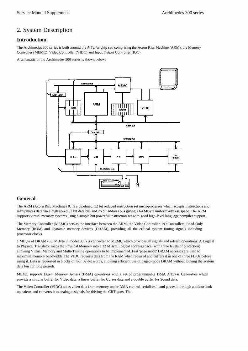
IntroductionThe Archimedes 300 series is built around the A Series chip set, comprising the Acorn Risc Machine (ARM), the Memory Controller (MEMC), Video Controller (VIDC) and Input Output Controller (IOC).
A schematic of the Archimedes 300 series is shown below:
GeneralThe ARM (Acorn Risc Machine) IC is a pipelined, 32 bit reduced instruction set microprocessor which accepts instructions and manipulates data via a high speed 32 bit data bus and 26 bit address bus giving a 64 MByte uniform address space. The ARM supports virtual memory systems using a simple but powerful instruction set with good high-level language compiler support.
The Memory Controller (MEMC) acts as the interface between the ARM, the Video Controller, I/O Controllers, Read-Only Memory (ROM) and Dynamic memory devices (DRAM), providing all the critical system timing signals including processor clocks.
1 MByte of DRAM (0.5 MByte in model 305) is connected to MEMC which provides all signals and refresh operations. A Logical to Physical Translator maps the Physical Memory into a 32 MByte Logical address space (with three levels of protection) allowing Virtual Memory and Multi-Tasking operations to be implemented. Fast 'page mode' DRAM accesses are used to maximise memory bandwidth. The VIDC requests data from the RAM when required and buffers it in one of three FIFOs before using it. Data is requested in blocks of four 32-bit words, allowing efficient use of paged-mode DRAM without locking the system data bus for long periods.
MEMC supports Direct Memory Access (DMA) operations with a set of programmable DMA Address Generators which provide a circular buffer for Video data, a linear buffer for Cursor data and a double buffer for Sound data.
The Video Controller (VIDC) takes video data from memory under DMA control, serialises it and passes it through a colour look-up palette and converts it to analogue signals for driving the CRT guns. The

Archimedes 300 series Service Manual Supplement
VIDC also controls all the display timing parameters and controls the position and pattern of the cursor sprite. In addition, it incorporates an exponential Digital to Analogue Converter (DAC) and stereo image table for the generation of high quality sound from data in the DRAM.
The VIDC is a highly programmable device, offering a very wide choice of display formats. The colour look-up palette which drives the three on-chip DACs is 13 bits wide, offering a choice from 4096 colours or an external video source.
The cursor sprite is 32 pixels wide and any number of rasters high. Three simultaneous colours (again from a choice of 4096) are supported and any pixel can be defined as transparent, making possible cursors of many shapes. It can be positioned anywhere on the screen. The sound system implemented on the device can support up to 8 channels, each with a separate stereo position.
The Input Output Controller (IOC) controls the I/O bus, expansion Podules and provides basic functions such as the keyboard interface, system timers, interrupt masks and control registers. It supports a number of different peripheral cycles and all I/O accesses are memory mapped.
The I/O systemThe I/O system is controlled by the I/O Controller IOC and the Memory Controller MEMC. The I/O Bus supports all the internal peripherals and the PODULE expansions. Details of the expansion bus can be found elsewhere in this manual.This section presents details of the I/O system for particular versions of the Archimedes series. It is intended to give the reader an understanding of Archimedes computers and should not be used to program the I/O system directly. The implementation details are liable to change at any time and only the published software interfaces should be used to manipulate the I/O system. It is important to realise that future systems may have a different implementation of the I/O system, and in particular the addresses (and number) of Podule locations may move. For this reason, and to ensure that any device may be plugged into any slot, all driver code for Podules must be relocatable. References to the direct Podule addresses should never be used. It is up to the machine operating system, in conjunction with the Podule ID to determine the address at which a Podule should be accessed. To this extent, some of the following sections are for background information only.
System Architecture
The I/O system (which includes podule devices) consists of a 16 bit data bus (BD[0:151) a buffered address bus (LA[2:21]) and various control and timing signals. The I/O data bus is independent from the main 32-bit system data bus, being separated from it by bidirectional latches and buffers. In this way the I/O data bus can run at much slower speeds than the main system bus to cater for slower peripheral devices. The latches between the 2 buses and hence the I/O bus timing are controlled by the I/O controller, IOC. The IOC caters for 4 different cycle speeds (slow, medium, fast and synchronous).A typical 300 series I/O system with 'simple' Podules fitted is shown in the diagram on page 8. The Podules are controlled by IOC. For clarity, the data and address buses are omitted from this diagram.
SYSTEM MEMORY MAPThe system memory map is defined by the MEMC, and is shown on page 9. Note that all system components, including I/O devices, are memory mapped.I/O SPACE MEMORY MAP
This IOC-controlled space has allocation for Simple Podules and External Podules.
DATA BUS MAPPING
The I/O data bus is 16 bits wide. Bytewide accesses are used for 8-bit peripherals. The I/O data bus (BD[0:15]) connects to the main system data bus (D[0:31]) via a set of bidirectional data latches.
The mapping of the BD[0:15] bus onto theD[0:31] bus is as follows:
During a WRITE (ie ARM to peripheral)BD[0:15] is mapped toD[16:31]
. During a READ (ie peripheral to ARM)BD[0:15] is mapped toD[0:15]

BYTE ACCESSES
To access bytewide podules, byte instructions are used. A byte store instruction will place the written byte on all four bytes of the word, and will therefore correctly place the desired value on the lowest byte of the I/O bus. A byte or word load may be used to read a bytewide podule into the lowest byte of an ARM register.HALF-WORD ACCESSES
To access a 16-bit wide podule, half-word instructions are used. When storing, the half-word is placed on the upper 16 bits,D[16:31]. To maintain upwards compatibility with future machines, half-word stores replicate the written data on the lower half-word,D[0:15]. When reading, the upper 16 bits are undefined.
PODULE IDENTIFICATION
It is important that the system is able to identify what podules (if any) are present, and where they are. This is done by reading the Podule Identification (PI) byte, or bytes, from the Podule Identification Field.
I/O ADDRESS MEMORY MAPPING
All I/O accesses are memory mapped. The IOC is connected as detailed in the table below:
IOC ARM
[OE] = [LA[21]]
[TM] = [LA[20]][T[0]] = [LA[19]][B[2]] = [LA[18]][B[1]] = [LA[17]][B[0]] = [LA[16]]
IOC address mapping

System memory map
9

Internal Register Memory Map
Programming DetailsEXTERNAL LATCH AThe External Latch A is a write only latch used to control parts of the floppy disc sub-system.

Peripheral address
Bit [0:3] US [0:3]
These bits select the floppy disc unit 0 through 3 when written LOW. Only one bit should be LOW at any one time.
Bit 4 Side Select
This controls the side select line of the floppy disc interface.
0 = Side 1 (upper)
1 = Side 0 (lower)
Bit 5 Floppy Motor ON/OFF Control
This bit control the floppy disc motor line. Its exact use depends on the type of drive.
Bit 6 In Use
This bit controls the INUSE line of the floppy disc. Its exact use depends on the type of drive.
Bit 7 Disc Eject
This controls the DISC EJECT or DISC CHANGED RESET line of the floppy disc drive.

Service Manual Supplement Archimedes 300 series
EXTERNAL LATCH BThe External Latch B is a write only register shared between several users who must maintain a consistent RAM copy. Updates must be made with IRQ disabled.
Bit [0:2] CD [0:2]CD[0:2] should be programmed LOW for future compatibility. CD [1] controls the floppy disc data separator format.
CD[1] = 0 Double Density CD[1] = 1 Single Density
Bit 3 FDCRThis controls the floppy disc controler reset line. When programmed LOW, the controller is RESET.
Bit 4 Printer StrobeThis used to indicate valid data on the printer outputs. It should be set HIGH when valid data has been written to the printer port and LOW after typically 5 µsec.
Bit [5:6] AUX [1:2]These bits allow the auxiliary I/O connector AUX [1:2] pins to be programmed.
Bit 7 HS3This bit controls the HS3 line of the hard disc interface. It allows extension of the ST506 interface to support up to 16 heads. It may be link selected to implement the standard ST506 "Reduced Write Current" function.
INTERRUPTSThe I/O system generates two independent interrupt requests, IRQ and FIQ. Interrupt requests can be caused by events internal to IOC or by external events on the interrupt or control port input pins.
The interrupts are controlled by four types of register, status, mask, request and clear. The status registers reflect the current state of the various interrupt sources. The mask registers determine which sources may generate an interrupt. The request registers are the logical AND of the status and mask registers and indicate which sources are generating interrupt requests to the processor. The clear register allows clearing of interrupt requests where appropriate. The mask registers are undefined after power up.
The IRQ events are split into two sets of registers A and B. There is no priority encoding of the sources.
Archimedes 300 series Service Manual Supplement
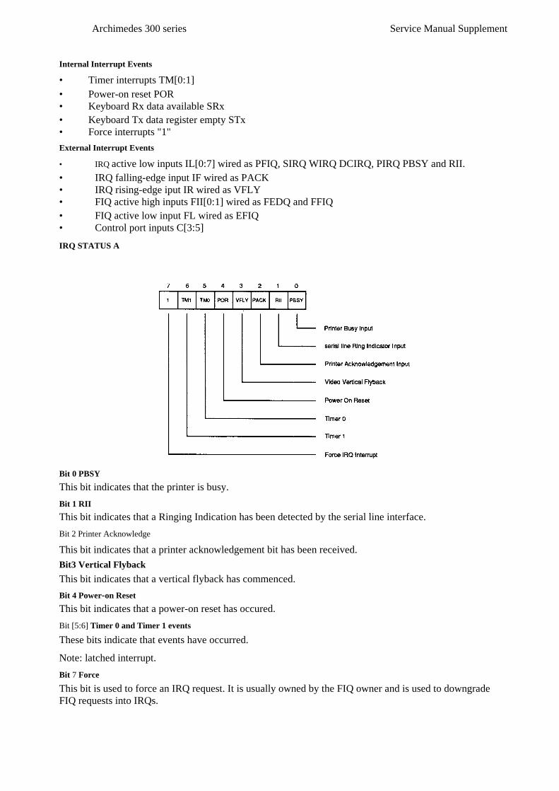
Internal Interrupt Events
• Timer interrupts TM[0:1]• Power-on reset POR• Keyboard Rx data available SRx• Keyboard Tx data register empty STx• Force interrupts "1"
External Interrupt Events
• IRQ active low inputs IL[0:7] wired as PFIQ, SIRQ WIRQ DCIRQ, PIRQ PBSY and RII.• IRQ falling-edge input IF wired as PACK• IRQ rising-edge iput IR wired as VFLY• FIQ active high inputs FII[0:1] wired as FEDQ and FFIQ• FIQ active low input FL wired as EFIQ• Control port inputs C[3:5]
IRQ STATUS A
Bit 0 PBSY
This bit indicates that the printer is busy.
Bit 1 RII
This bit indicates that a Ringing Indication has been detected by the serial line interface.
Bit 2 Printer Acknowledge
This bit indicates that a printer acknowledgement bit has been received.
Bit3 Vertical Flyback
This bit indicates that a vertical flyback has commenced.
Bit 4 Power-on Reset
This bit indicates that a power-on reset has occured.
Bit [5:6] Timer 0 and Timer 1 events
These bits indicate that events have occurred.
Note: latched interrupt.
Bit 7 Force
This bit is used to force an IRQ request. It is usually owned by the FIQ owner and is used to downgrade FIQ requests into IRQs.

Service Manual Supplement Archimedes 300 series
IRQ STATUS B
Bit 0 Podule FIQ request (PFIQ)
This bit indicates that a Podule FIQ request has been received. It should usually be masked OFF.
Bit 1 Sound buffer swap (SIRQ)
This bit indicates that the MEMC sound buffer pointer has been relocated.
Bit 2 Serial line controller (SLCI)
This bit indicates that 65C51 serial line controller interrupt has occurred.
Bit 3 Winchester interrupt
This bit indicates that a Winchester (Hard disc) interrupt has occurred.
Bit 4 Disc Changed Interrupt (DCIRQ)
This bit indicates that the floppy disc has been removed.
Bit 5 Podule interrupt request (PIRQ)
This bit indicates that a Podule IRQ request has occurred.
Bit 6 Keyboard transmission event
This bit indicates that the keyboard transmit register is empty and may be reloaded.
Bit 7 Keyboard reception event
This bit indicates that the keyboard reception register is full and may be read.

Archimedes 300 series Service Manual Supplement
INTERRUPT STATUS FIQ
Bit 0 Floppy disc data request (FFDR)This bit indicates that a Floppy Disc Data Request has occurred.
Bit 1 Floppy disc interrupt request (FFTIQ)This bit indicates that a Floppy Disc Interrupt Request has occurred:
Bit 2 Econet Interrupt request (EFIQ)This bit indicates that an Econet Interrupt Request has occurred.
Bit [3:5] C[3:5]See IOC data sheet for details.
Bit 6 Podule FIQ request (PFIQ)This bit indicates that a Podule FIQ Request has occurred.
Bit 7 ForceThis bit allows an FIQ interrupt request to be generated.
CONTROL PORT
The control register allows the external control pins C[0:5] to be read and written and the status of the PACK and VFLY inputs to
be inspected. The C[0:5] bits manipulate the C[0:5] I/O port. When read, they reflect the current state of these pins. When written
LOW the output pin is driven LOW. These outputs are open-drain, and if programmed HIGH the pin is undriven and may be
treated as an input.
On reset all bits in the control register are set to "1".

Service Manual Supplement Archimedes 300 series
C[7] (VFLYBK) and Test Mode
C[7] allows the state of the (VFLYBK) signal to be inspected. This bit will be read HIGH during vertical flyback and LOW during display. See VIDC datasheet for details. This bit MUST be programmed HIGH to select normal operation of the chip.
C[6] (PACK) and Test Mode
C[6] allows the state of the parallel printer acknowledge input to be inspected. This bit MUST be programmed HIGH to select normal operation of the the chip.
C[5] (SMUTE)This controls the muting of the internal speaker. It is programmed HIGH to mute the speaker and LOW to enable it. The speaker is muted on reset.
C[4] (C4)C[4] is available on the Auxiliary I/O connector.
C[3]C[3] is reserved and should be programmed HIGH.
C[2] (READY)C[2] is used as the floppy disc (READY) input and must be programmed HIGH.
C[1:0] SDA, SCL The VC Bus
The C[0:1] pins are used to implement the bi-directional serial I2C bus to which the Real Time Clock and battery RAM are connected.
The Sound SystemThe sound system is based on the VIDC stereo sound hardware. External analogue anti-alias filters are used which are optimised for a 20 kHz sample rate. The high quality sound output is available at a 3.5mm stereo jack socket at the rear of the machine which will directly drive personal stereo headphones or alternatively an amplifier and speakers. A mono mix of the sound output is sent to the internal loudspeaker. In addition, an unfiltered stereo signal is available at the Auxiliary Audio connector on the main board.
THE VIDEO CONTROLLER SOUND SYSTEM HARDWARE
VIDC contains an independent sound channel consisting of the following components: A four-word FIFO buffers sixteen 8-bit sound samples with a DMA request issued whenever the last byte is consumed from the FIFO. The sample bytes are read out at a constant sample rate programmed into the 8-bit Audio Frequency Register; which may be programmed to allow samples to be output synchronously at any integer value between 3 and 255 microsecond intervals .
The sample data bytes are treated as sine plus seven-bit logarithmic magnitude and after exponential digital to analogue conversion, de-glitching and sign-bit steering, are output as a current at one of the audio output pins to be integrated and filtered externally.
VIDC also contains a bank of eight stereo image position registers each of 3 bits. These 8 registers are sequenced through at the sample rate with the first register synchronised to the first byte clocked out of the FIFO. Every sample time is divided into eight time slots and the three bit image value programmed for each register is used to pulse width modulate the output amplitude between the LEFT and RIGHT audio current outputs in multiples of time slot subdivisions. This allows the signal to be spatially positioned in one of seven stereo image positions.
THE MEMORY CONTROLLER SOUND SYSTEM HARDWARE
MEMC provides three internal DMA address registers to support Sound buffer output; these control the DMA operations performed following Sound DMA requests from VIDC. The registers allow the physical addresses for the START, PNTR (incremental) and END buffer pointers to a block of data sample in the lowest half Megabyte of physical RAM to be accessed. These operate as follows: programming a 19-bit address into the PNTR register sets the physical address from which sequential DMA reads will occur (in multiples of 4 words) and programming the END pointer sets the last physical address of the buffer. Whenever the PNTR register increments up to this END value the address programmed into the START
16

Archimedes 300 series Service Manual Supplement
register is automatically written into the PNTR register for the DMA to continue with a new sample buffer in memory. A Sound Buffer Interrupt (SIRQ) signal is generated when the reload operation occurs which is processed by IOC as a maskable interrupt (IRQ) source.
The Memory Controller also includes a sound channel enable/disable signal. Because this enable/disable control signal is not synchronised to the sound sampling requests will normally be disabled after the waveforms which are being synthesised have been programmed to decay to zero amplitude; the last value loaded into the Audio data latch in the VIDC will be output to each of the Stereo image positions at the current Audio Sample rate.
THE I/O CONTROLLER SOUND SYSTEM HARDWAREIOC provides a programmed output control signal which is used to turn the internal speaker on or off, as well as an interrupt enable/status/reset register interface for the Sound Start Buffer reload signal generated by the Memory Controller.
The internal speaker may be muted by the control line SMUTE which is driven from the IOC output C5. On reset this signal will be taken high and the internal speaker will be muted.
The stereo output to the Hi-Fi stereo output is not muted by SMUTE and will always reflect the current output of the DAC channels.
The Keyboard
The ARM to keyboard connection is essentially a half duplex connection with handshaking by the ARM, plus a small amount of command protocol by the ARM. When the keyboard has sent a byte, in normal operation, it will not send again until it has received an Ack from the ARM. The only exception to this is during the reset protocol used to synchronise the handshaking, where each side is expecting specific responses from the other, and will not respond further until it has those.
In addition to this simple handshaking system, the keyboard will not send mouse data unless specifically allowed to, as indicated by Ack Mouse, which allows the transmission of one set of accumulated mouse coordinate changes, or the next move made by the mouse. While it is not allowed to send mouse changes the keyboard will buffer mouse changes.
A similar handshake exists on key changes, transmitted as key up and key down, and enabled by Ack Scan. At the end of a keyboard packet (two bytes) ARM should always perform an Ack Scan as there is no protocol for re-enabling later. With the mouse, the ARM may request mouse data some time later by means of Request Mouse Position (RQMP).
KEY CODESThe keyboard identifies each key by its row and column address in the keyboard matrix. Row and column codes are appended to the key up or down prefix to form the complete key code.
e.g. 'Q' key down, the complete row code is 11000010 (C2 hex) and the column code is 11000111 (C7 hex).
Note: Eight keys have N key roll over. The ARM is responsible for implementing two-key rollover, therefore the keyboard transmits all key changes (when enabled). The keyboard does not operate any auto-repeat, only one down code is sent, at the start of the key down period.
Operating voltage range (measured at the cable plug) is 5 V ±0.5 V. Maximum current consumption of the of the keyboard is 60 mA (note that the mouse may use up to an additional 100 mA).
A maximum delay of 100ms is permissible from release of the reset switch to the first keyboard transmission of HRST.
SERIAL INTERFACEInformation on the keyboard status is sent to the ARM via a serial data link using NRZ encoding. Command and acknowledge codes are similarly sent from the computer to the keyboard along a serial data link. The two links form a full duplex system which operates at 31.25 k baud. Each data byte (eight data bits) is preceded by a single start bit (Logic 1). The least significant data bit (DO) is sent first. The last data bit (D7) is followed by two stop bits (Logic 0). Note that data is sent in inverted form, that is a logic 1 data bit will appear on the serial line as a logic 0 and vice versa.
When idle the line is held at a logic 0 level.
17

Service Manual Supplement Archimedes 300 series
Serial INPUT/OUTPUT characteristics
Serial line signals are CMOS compatible. The data line logic input has a nominal switching threshold of 50% of the supply voltage, to minimise skew between rising and falling edges. Signal hysteresis is provided on input lines, to minimise noise susceptibility.
SERIAL DATA PROTOCOL
Serial data transmissions from the keyboard are either one or two bytes in length. Each byte sent is individually acknowledged by the ARM. The keyboard will not transmit a byte until the previous byte has been acknowledged, unless it is the HRST code indicating that a power on or user reset occurred or that a protocol error occurred; see below.
Reset ProtocolThe keyboard restarts when it receives a HardReSeT (HRST) code from the ARM. To initiate a restart the keyboard sends a HRST code to the ARM, which will then send back FIRST to command a restart. The keyboard sends HRST to the ARM if :
A power on reset occurs A
User reset occurs
A protocol error is detected
After sending FIRST, the keyboard waits for a HRST code. Any non HRST code received causes the keyboard to resend HRST. The pseudo program below illustrates the reset sequence or protocol.
Note, the on/off state of the LED's does not change across a reset event, hence the LED state is not defined at power on. The ARM is always responsible for selecting the LED status. After the reset sequence, Key scanning will only be enabled if a scan enable acknowledge (SACK or SMAK) was received from the ARM.

Archimedes 300 series Service Manual Supplement
Data Transmission
When enabled for scanning, the keyboard informs the ARM of any new key down or new key up by sending a two byte code incorporating the key row and column addresses. The first byte gives the row and is acknowledged by a byte acknowledge (BACK) code from the ARM. If BACK was not the acknowledge code then the error process (ONerror) is entered. If the BACK code was received the keyboard sends the column information and waits for an acknowledge. If either a NACK,SACK, MACK or SMAK acknowledge code is received, the keyboard continues by processing the ack. type and selecting the mouse and scan modes implied. If the character received as the second byte acknowledge was not one of NACK/MACK/SACK/SMAK then the error process is entered.
Mouse DataMouse data is sent by the keyboard if requested by a RQMP request from the ARM or if a SMAK or MACK have enabled transmission of non-zero values. Two bytes are used for mouse position data. Byte one encodes the accumulated movement along the X axis while byte two gives Y axis movement.
Both X and Y counts must be transferred to temporary registers when data transmission is triggered, so that accumulation of further mouse movement can occur. The X and Y counters are cleared upon each transfer to the transmit holding registers. Therefore, the count values are relative to the last values sent. The ARM acknowledges the first byte (Xcount) with a BACK code and the second byte (Ycount) with any of NACK/MACK/SACK/SMAK. A protocol failure causes the keyboard to enter the error process (ONerror).
When transmission of non-zero mouse data is enabled, the keyboard gives Key data transmission priority over mouse data except when the mouse counter over/underflows.
Acknowledge Codes
There are seven acknowledge codes which may be sent by the ARM. RAK1 and RAK2 are used during the reset sequence. BACK is the acknowledge to the first byte of a two byte keyboard data set. The four remaining types, NACK/MACK/SACK and SMAK, acknowledge the final byte of a data set. NACK disables key scanning and therefore key up/down data transmission as well as setting the mouse mode to send data only on RQMP request. SACK enables key scanning and key data transmission but disables unsolicited mouse data. MACK disables key scanning and keydata transmission and enables the transmission of mouse count values if either X or Y counts are non-zero. SMAK enables key scanning and both key and mouse data transmission. It combines the enable function of SACK and MACK.
While key scanning is suspended (after NACK or MACK) any new key depression is ignored and will not result in a key down transmission unless the key remains down after scanning resumes following a SACK or SMAK. Similarly a key release is ignored while scanning is off.
Command may be received at any time. Therefore, commands can be interleaved with acknowledge replies from the ARM, eg keyboard sends KDDA (1st byte), keyboard receives command, keyboard receives BACK, keyboard sends KDDA (2nd byte), keyboard receives command, keyboard receives SMACK. If the HRST command is received the keyboard immediately enters the restart sequence, see (ONrestart). The LEDS and PRST commands may be acted on immediately. Commands which require a response are held pending until the current data protocol is complete. Repeated commands only require a single response from the keyboard.

Service Manual Supplement Archimedes 300 series
ARM COMMANDS
Code values
x is a data bit in the Code e.g. xxxx is a four bit data field
INTERCONNECTION CABLE
The interconnection cable has stranded conductors, suitable for operation at 5 V, 200 mA per conductor.

Archimedes 300 series Service Manual Supplement
MOUSE INTERFACEThe mouse interface has three switch sense inputs and two quadrature encoded movement signals for each of the X axis and Y axis directions. Mouse key operations are debounced and then reported to the ARM using the Acorn key up / key down protocol. The mouse keys are allocated unused row and column codes within the main key matrix.
Switch 1 (left) Row code - 7 Column code - 0
Switch 2 (middle) Row code - 7 Column code - 1
Switch 3 (right) Row code - 7 Column code - 2
e.g. Switch 1 release would give 11010111 (D7 hex) as the complete row code, followed by 11010000 (DO hex) for the column code.
Note: Mouse keys are disabled by NACK and MACK acknowledge codes, and are only enabled by SACK and SMAK codes, ie they behave in the same way as the keyboard keys.
The mouse is powered from the keyboard 5 V supply and may consume up to 100 mA. The keyboard design ensures that the power supply volatge at the mouse connecr=tor is within ±150 mV of the voltage supplied at the keyboard cable plug. Sufficient power supply decoupling is provided to ensure that connection and disconnection of the mouse from the keyboard does not affect normal keyboard operation.
Movement Signals
Each axis of movement is independently encoded in two quadrature signals. The two signals are labelled REFerence and DIRection (e.g. X REF and X DIR). The table below defines the absolute direction of movement. Circuitry in the keyboard decodes the quadrature signals and maintains a signed 7 bit count for each axis of mouse movement.
Initial NextState State
REF DIR REF DIR
1 1 1 0 }1 0 0 0 } Increase count by one0 0 0 1 } for each change of state.0 1 1 1 }
1 1 0 1 }0 1 0 0 } Decrease count by one0 0 1 0 } for each change of state.1 0 1 1 }
When count overflow or underflow occurs on either axis both X and Y axis counts lock and ignore further mouse movement until the current data has been sent to the ARM.
Overflow occurs when a counter holds its maximum positive count (0111111 binary). Underflow occurs when a counter holds its maximum negative count (1000000 binary).

Service Manual Supplement Archimedes 300 series
KEY SWITCH MAPPING
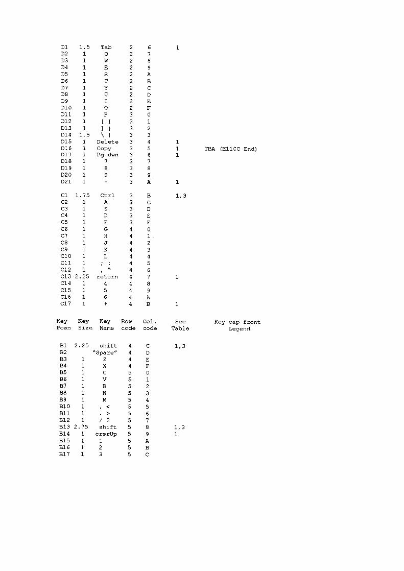

Row and column codes are in Hexadecimal Key positions are as shown on page 22. Key position with N key rollover.Green light emitting diode under key cap.
Archimedes 300 series Service Manual Supplement
3. UpgradesDetails of upgrades available for Archimedes 300 series computers are given in the Module Level Service Manual, as follows:
Backplane and Fan
Econet ModulePodule Installation Leaflet0.5Mbyte RAM Upgrade Instructions Second Floppy Disc Upgrade Instructions Hard Disc Upgrade InstructionsHard Disc Upgrade Installation Leaflet MIDI Module Installation LeafletArthur ROM Fitting Instructions
3.1 Hard Disc Drive Interface
The following describes the Hard disc interface circuitry incorporated onto the Archimedes model 440 main PCB. It applies equally to the Hard disc Podule fitted as an upgrade to Archimedes 300 series units, with the exception of the IC component reference numbers and the Archimedes standard Podule ID circuitry which is fitted to the Podule version only.
CIRCUIT DESCRIPTION
All functions of the Hard disc drive are controlled by the Hitachi HD63463 Hard disc Controller chip (IC22).
Host ConnectionThis device is connected to the system CPU by means of the 16 bit I/O bus. It is memory-mapped from address &032D0000 to &032D0028 (nb: these addresses are different for the Hard disc Podule, which are slot-dependant). The only unusual feature of this circuit is the use of an address line for the HD63463 read/write line. This is necessary to allow the host CPU to simulate DMA cycles, during which this line reverses its function.
Reset is provided by the host system, as is the 8 MHz clock (CLK8) from which all host communication signal timing is derived.
ST506 Hard Disc IntefaceThe connection to the Hard disc drive is an implementation of the standard ST506 interface. Drive control signals are provided on a 34-way bus which may be daisy-chained for up to four Hard disc drive units, and data is transferred on a separate 20-way cable for each drive in the system.
Before any data transfer can take place between the Hard disc drive and the HD63463, the correct drive and correct read/write head in that drive must be selected. This is achieved by two drive select lines and three head select lines, all buffered by a 7406 (IC33). Having selected the drive, the HDC (Hard Disc Controller) will check the READY line before proceeding with the required function. A failure of this signal (or the SEEK COMPLETE signal, see below) may result in a polling action (ie repeated attempts to select) by the HDC. All control signals on the 34-way bus from a Hard disc unit will only be active when the drive is selected.
If a seek is required before selecting the read/write head then the direction signal DIR will be set high or low to indicate movement in or out and the requisite number of step pulses transmitted on the STEP

Service Manual Supplement Archimedes 300 series
control line. The HDC must then wait for the SEEK COMPLETE (SC) signal to be returned from the drive unit. As previously mentioned, the HDC may go into a polling action while waiting for this signal.
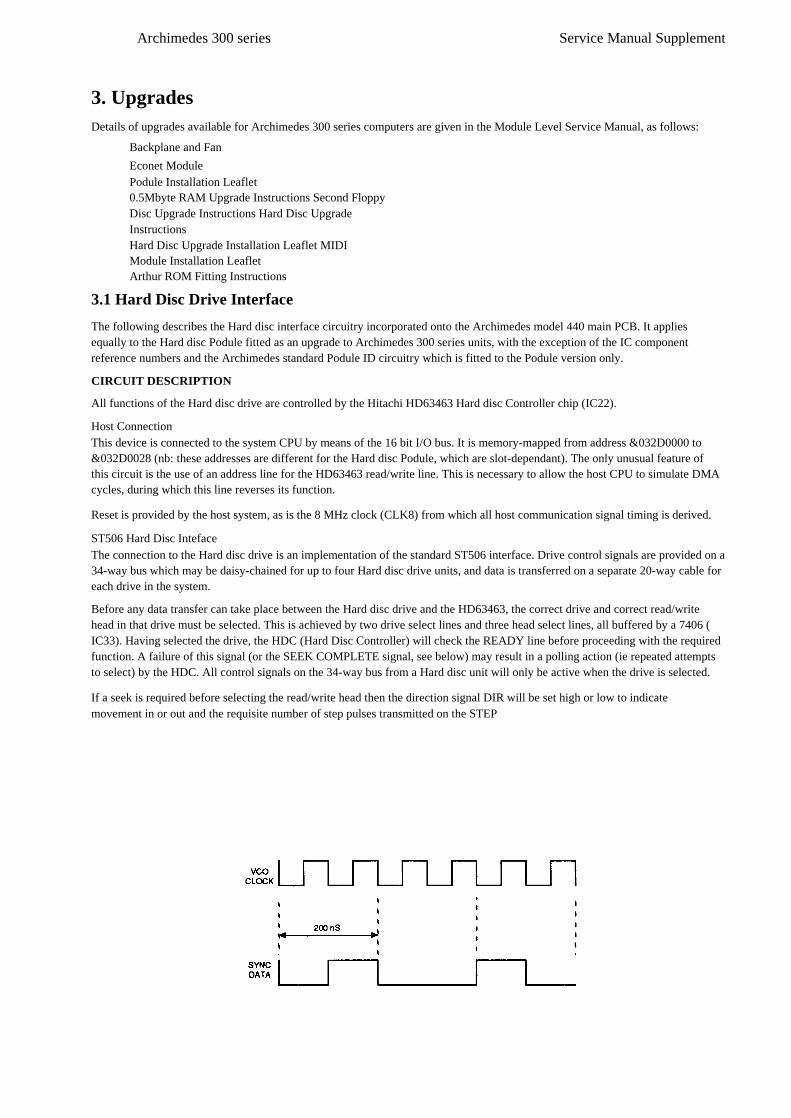
All control signals to the drive are buffered by the 7406 (IC33) and all signals from the drive are buffered by a 74HCT14 (inverting Schmitt trigger), IC32. Demultiplexing and buffering of the direction (DIR), step and reduced write current (RE+WC) signals is achieved by a 7438 (IC34).Read Data PathRead data is received from the drive as a differential signal and applied to the differential receiver 26LS32 (IC39). From here it passes through a multiplexer (this circuit can control two Hard disc drives) and onto the data separator circuit.Data SeparatorThe data from the Hard disc drive takes the form of a stream of pulses whose position with respect to a clock signal defines their meaning, binary 1 or 0. The nominal frequency of this clock is 10 MHz although it may have to vary slightly to compensate for variations in disc speed and/or disk wobble. Since this clock signal is not provided by the Hard disc drive it has to be generated by the interface circuitry. The Data-Separator contains a voltage controller oscillator NCO), some filter components and an input for a crystal controlled 10 MHz clock. When the HDC is not trying to read data from the Hard disc drive, the VCO is locked onto the 10 MHz crystal clock.To read data the HDC first asserts the read-gate signal (RGATE), this causes the data-separator DP8455 (IC50) to attempt to adjust the VCO frequency and phase until the VCO cycles are in quadrature with the data pulses when they are present.
When the data separator has detected valid preamble (a special pattern of Os and 1s) it asserts lock-detect (LD) which enables the now synchronised data stream to the HDC. In turn, when the HDC sees a special data pattern called an address mark it asserts SYNC. This signal is linked back to the data separator and used to slow down the tracking action of the VCO during the actual read process.
Write DataWrite data timing is synchronised to the 10 MHz crystal oscillator. The data emerges from the bi-directional data pin RWDATA on the HDC and is fed to a delay line (IC42) which is a 50 nS 5-tap device. This gives three identical versions of the write data stream separated in time by 10 nS. These three signals are fed to a multiplexer 74HCT153 (IC41) which selects the appropriate version of the write data stream when manipulated by the write-precompensation control lines EARLY and LATE. Finally, the data is passed through a differential driver 26LS31 (IC40) before going on to the Hard disc drive itself.FormatData is stored in the form of sectors. There are 32 sectors on each track and 4 tracks in each cylinder.A sector has an ID (identity) field and a DATA field. The ID field contains the sector's number and the DATA field contains the data stored in that sector.
Before data can be written to the data field of a sector, the correct sector must be located by repeated reading of ID fields on the track until the required sector is found.
3.2 MIDI PoduleThe MIDI Podule is a single Eurocard sized plug-in card for the Archimedes range of computers. The Podule offers users access to the wide range of synthesisers, keyboards and other instruments which use the MIDI standard for communication between system units.
The following circuit description of the MIDI Podule does not cover operating software or MIDI protocols. For operational details, see the Acorn MIDI User Guide.
The Podule connects to the Archimedes computer via the computer's internal backplane. Conection is via a DIN standard PCB mounted plug fitted with 64 contacts in a 96 way housing. Connector rows a and c are populated. Refer to the circuit diagram for pinout details.
CIRCUIT DESCRIPTIONOn the PCB are eight ICs. The principle device is IC5, an SCC 2619 UART. The UART, under control of software running on the Archimedes computer, sends and receives MIDI serial data at the required 32.5 K Baud rate. Input serial data is optically isolated by IC6, a 6N138. Diode Dl protects against reverse
26

Archimedes 300 series Service Manual Supplement
polarity of the normally unipolar signal. Resistor R6 sets the working current for the opto LED, in conjunction with the source impedance of the external MIDI driver.
IC7, an open drain collector TTL Hex inverter, is used for signal buffering and to drive the MIDI 'out' and 'through' sockets.
Buffered MIDI data feeds directly to the Receive data pin of the UART IC5 and, via a separate open collector gate IC7, to the 'through' output socket.
MIDI 'out' data is buffered (IC7) onto two output sockets SK3 and SK4, the data is the serial stream output from the UART IC5.
To conform to the Archimedes Podule specification, the MIDI Podule is equipped with a Byte wide EPROM IC2. IC2 contains the Podule ID and low level driver code (which is down-loaded into the main computer memory for execution). Optional large EPROMs are supported by a paging system, using IC3, a 273 octal latch. Links 1, 2 and 3 are preset (cuttable tracks) for a 27128 EPROM. See the table below for alternative options. Note that the PCB is tracked for a 32 pin EPROM but normally assembled with a 28 pin socket so a 27512 is the largest EPROM easily fitted.
Example type Size LK1 LK2 LK3
27128 16kByte 5 V 5 V 5 V
27256 32 kByte 5 V 5 V PA327152 64 kByte PA4 5 V PA327C101 128 kByte PA4 N.C. PA3
256 kByte PA4 PA6 PA3512 kByte PA4 PA6 PA3
The 74HCT32 (IC8) and 74HCT138 (IC4) decode the address space occupied by the EPROM, the page patch (IC3) and the UART (IC5). Finally, the 74HCT245 (ICI) buffers data to and from the backplane data lines BDO through BD7.
The Archimedes computer hardware reset is used on the Podule to clear the page latch IC3 to a known state, ie zero, as well as resetting the UART. For full details of the effect of reset on the UART, refer to the Signetics SCC2619 data sheet.
The UART is clocked continuously at 2 MHz, internal programmable dividers derive the serial data (baud) rate from the 2 MHz clock.
Any access made to the Podule slot (notPS at logic zero) occupied by the MIDI Podule will enable the data bus buffer IC1, data direction being set by the logic level of the PR/notW line. The internal device access is then selected by IC4 decoding LAl2 with LA13 high and notPS low, or by part of IC8 if LA13 is low.
LA13 low selects the EPROM for read access. Note that there is no protection from bus conflicts if an attempt to write to the EPROM occurs.
LA13 high selects the UART is LAl2 is low, or the Page latch IC3 if LAl2 is high, IC8 gates in notPWE to ensure the page latch is write only.
3.3 I/O Podule
For details of the I/O podule and the optional MIDI module, see the information supplied in the manual accompanying the Podule upgrade kit.
3.4 Econet Module
Econet systems can only be serviced properly by Econet service centres, who will have the necessary test equipment to check the system thoroughly. However, there are some simple checks which can be made without the test equipment. See the Econet board circuit diagram in the Appendix.
Check that the module is installed and fitted correctly. Check that the two connectors on the Econet module are correctly inserted. The longer connector has two spare pins on the left of the PCB socket. If the module is displaced and plugged into one or both of these pins, it will not work.
27

Service Manual Supplement Archimedes 300 series
4. Fault-finding informationSee the 300 Series Module Level Service Manual for :
Dealer Test Software test instructions (section 7.4) Main PCB circuit diagram (pages 80/81)Main PCB test point and layout diagrams (pages 76 and 77).
The purpose of this fault-finding information is to enable the engineer to trace faults to module level and, unless the module is non- serviceable, to component level. The modules are defined as the:
Main PCB,
PSU*Floppy disc drive(s)+
Hard disc drive (where fitted)+ Podule(s), as fittedPodule backplaneKeyboard**Mouse*Monitor+
* These are available as service-replacement only items and are non-serviceable. ** These are part-serviceable but include service-replacement only items.
+ These items are third party units, for which service information is available separately.
It is important to determine as closely as possible the nature and location of the fault in order to identify the faulty module.
Basic test equipment required:
100 MHz oscilloscope DC VoltmeterContinuity tester
In all instances, follow through the checks until the fault is located and identified, then change or repair the appropriate module. For information on module replacement procedures, etc., see the Acorn Service and Support Strategy document.
IMPORTANT NOTE
WHEN REFITTING OR FITTING A REPLACEMENT ASSEMBLY, CHECKS SHOULD BEMADE FOR EARTH CONTINUITY BETWEEN THE EARTH PIN OF THE MAINS PLUG
AND THE FOLLOWING:
THE BASE METALWORK
THE REAR PANELS (INCLUDING BLANKING PANELS)
THE TOP COVER
USE AN EARTH CONTINUITY TESTER SET TO 25 AMPS.
CAUTIONREPAIRS TO MULTI-LAYER PCBs
The main PCB is a four-layer board. Components should only be removed from the board using equipment specifically designed for this purpose. For details of suitable equipment available, contact Acorn Computers Ltd.

Archimedes 300 series Service Manual Supplement
4.1 Basic checks
4.1.1 FIRST, CHECK THE OBVIOUS:With both the monitor and the computer switched on, check for POWER ON indications (computer and monitor ON LEDs). If neither have power, check the main fuse in the wall plug.
If the computer is powered but not the monitor, check for power on the AC outlet socket at the rear of the computer main unit by plugging in a known good monitor. Should this also fail, replace the computer power supply.
If the monitor is powered but not the computer, an internal power supply fuse may have blown. Replace the PSU.
If both have power, check by substitution that the monitor and the interconnection cable are serviceable. Check for the correct
power supply output voltages on the main PCB:
PL5 = +12 V; PL6 = 0 V; PL7 = 5 V and PL8 =-5 V
If the power supply is emitting a clicking sound, this indicates either a short between two of its outputs or a faulty power supply.
Make sure all of the ROMs are inserted correctly and that the relevant links (LK2, LK6 and LK12) are correct for the type of ROMs used. The options and settings of these links are detailed in section 5, "Connectors, interfaces, links and test points", in the Module Level Service Manual.
The keyboard CAPS LOCK light should toggle on and off when pressed and assuming a disc is present, the disc drive light will glow after a *CAT command. If so, this indicates that the system is alive and that the failure is confined to the video circuitry. See section 4.3.1.
If there is no response, substitute a known good keyboard and repeat the check. If there is still no response, there is a system failure - see section 4.3.2. If the substitute keyboard restores normal working, change the original keyboard PCB.

Service Manual Supplement Archimedes 300 series
4.1.2 FLOW CHARTSThe following flow charts will be useful aids to basic checks:
NO DISPLAY
* See Appendix 7.4 in the Module Level Service Manual
30

Archimedes 300 series Service Manual Supplement
NO SOUND
*TEST PROGRAM:
10 REM > Check all channels20 VOICES 830 FOR channel=1 TO 840 OSCLI("Channelvoice "+STR$(channel)+" "+STR$(2))50 NEXT60 FOR channel = 1 to 870 SOUND channel, -15, 100,2480 PRINTchannel90 k=GET100 NEXT
RUN PROGRAM.PRESS A KEY AND REPEAT 8 TIMES.PRINTS CHANNEL NUMBER ON SCREEN AND PLAYS VOICE 2 FOR EACH CHANNEL.

Service Manual Supplement Archimedes 300 series
4.2 Run main PCB Functional TestAction resulting from test failure
The following notes refer to the test procedures on the PCB functional test disc, and the action that should be taken as the result of a test failure.Type/Model: Memory area fault -
Perform memory tests, section 4.9, and repair as necessary.
Memory: Repair as above.
Battery-
backed RAM: Perform "NVM and RTC' tests, section 4.4.6, and repair as necessary.
Loudspeaker: If no sound, check speaker connections. Substitute a known good speaker and re-test. If OK, replace speaker. If test still fails,perform "AUDIO" tests, section 4.4.5, and repair as necessary.
Headphones: If no sound or poor/faulty sound on known good headphones, perform AUDIO tests and repair as necessary. See also Production and Field Changes, Appendix section 5.2.
Monitor Screen: If display rolls or is unstable, perform 'R' reset until correct default value obtained. If no improvement, perform "Unstable or Scrolling Display" tests, section 4.3.3, and repair as necessary.
If the display breaks up around its edges and spurious characters appear suspect the system oscillator. See "Corrupted Display", section 4.3.4.Colours incorrect or missing -With a full white screen, VIDC IC 17 pins 39, 40 and 41 should all have the same signal on them. If not, change the VIDC IC17.
Floppy Disc: See "Floppy disc drive", section 4.4.2.
Serial port If test fails,see "Serial Port, section 4.4.4". If a fault is reported but the test is passed, see the Serial Port Application Note in the Appendix for possible explanations.
Printer: See "Printer", section 4.4.3.
4.3. Main PCB faults
4.3.1 VIDEO FAILURECheck for +5 V on both ends of L1, if open circuit then check C14 for short circuit. Also check for 3.5 Volts (approx.) on IC 17 pin 43. Should this not be present then check R67.
Check for a 24 MHz clock on IC 17 pin 19. If missing then check continuity to and through P13a and its shunt.
Check for video data on IC 17 pins 39, 40 and 41. If not present, check power supply to IC 17 before finally changing IC 17.Check for short circuits on signals VIDRQ and VIDAK.
Check connection of all data lines to VIDC.
6.3.2 SYSTEM FAILUREIn order to eliminate the major devices first, change in turn the ARM IC 43, MEMC IC 45, IOC21 and VIDC IC17. If the system still appears to be dead, proceed as follows:
Check for main system clock of 24 MHz on LK1 position c or d. If absent, check again on IC 15 pins 2 or 3 and change IC15 if required. Finally, change the crystal XL2.
Check for clocks on IC45 pion 67 and IC17 pin 19.
Check that the signal RST driving IC 45 pin 44 and IC 43 pin 9 is not stuck high.
32

Archimedes 300 series Service Manual Supplement
Check for the presence and validity of the processor addresses and PHI 1 clock. This can be done by examining the signals on IC 36 pins 12 to 19, IC 35 pins 12 to 19 and IC 28 pins 16 to 19, whilst holding down the RESET button on the keyboard. In this situation the processor continuously increments its address bus. Should any of the signals not toggle, suspect either a short or open circuit on that line. Should none of the signals toggle, check for the PHI 1 clock on the appropriate IC and at its source on Q15 emitter and IC 45 pin 66. Also check to see that addresses are being presented to the inputs of the above devices. Change ICs 36, 35 or 28 as appropriate, or if no addresses are present, change the ARM IC 43.
The data bus can be inspected by probing on resistors R141 to 172. By their nature, it is difficult to interpret the signals seen, so just check for the ability of the signals to move between logic states. None of these lines should be stuck permanently high, low or in a midrail state. Any of these resistors may be removed in order to isolate the DRAM bank from the CPU, thus easing the tracing of shorts, etc. Also check for short or open circuits on the BDATA bus, IC 11 pins 12 to 19 and IC 19 pins 12 to 19.
Check for shorts on DRAM address bus, either on the DRAMS themselves or on IC 45 pins 28 to 36.
Check for Data and Address signals on all four of the ROMs. This is especially important if an ARTHUR ROM upgrade has been carried out, as misuse of a screwdriver during ROM removal may have damaged or broken PCB tracks.
Check for all address lines on MC, again with RESET held down.
Check the processor interrupt lines FIQ and IRG pins 8 and 7 on ARM IC 43. Neither of these should be stuck low. IRQ can be expected to pulse low, FIQ should be high. These interrupts should also be checked at their source on IOC IC 21 pins 50 and 51. Should these also be low, the interrupt source can be traced by examining all interrupt inputs to IOC IC 21 on pins 30 to 42 (note that pins 30, 31 and 42 are active high logic).
Check for short or open circuits on the latched 1O data bus, IC11 pins 12 to 19 and IC19 pins 12 to 19. This may well cause a false interrupt condition to occur.
Check corner pins of IOC IC21 for short circuits. Check for a
RAS signal on pin 5 of all the DRAMS.
4.3.3 UNSTABLE OR SCROLLING DISPLAYThe computer may have lost its configuration value for SYNC. Type at the keyboard:
*CON. SYNC 1 (RETURN)
press reset RESET and see if if any change occurs. Investigate configuration failure as detailed in section 4.4.6.
Check for CSYNC signal on SK2 pin 4. If not present, trace back through LK10, R7 and IC4, finally changing VIDC IC17.
4.3.4 CORRUPTED DISPLAYIf the display breaks up around its edges and spurious characters appear then investigate the system oscillator. Replace XL2.
Check DRAM using the main memory test routines, section 4.9.
4.3.5.COLOURS INCORRECT OR MISSINGWith a full white screen, VIDC IC17 pins 39, 40 and 41 should all have the same signal on them. If not, change the VIDC IC17.
Trace each signal through the periphery circuitry and out to SK2 until the fault is found. Check that IC4 pin
2 is responding to its input on pin 1 (pulls low only).
Make sure that the configuration items "BAUD" and "DATA" are set to sensible values. Check for -5 V on IC7 pin 8 and R12 to R15. Check for the clock on IC9 pins 6 and 7, change XL1 if faulty. Change ICs 7 and 6.

Service Manual Supplement Archimedes 300 series
4.4 Peripheral area faults
4.4.1 KEYBOARD AND MOUSE
Make sure that the configuration items "DELAY" and "REPEAT" are set to sensible values - see the Archimedes Welcome Guide.
Check computer interface by swapping to a known good keyboard and mouse. If failure still present, check continuity of keyboard connector SK 12 and ensure that +5 V can be found on pin 4 and 0 v on pin 3.
Check functionality of inverting buffers in IC 20, check continuity through R 176 and R 180. Replace IOC IC 21.
4.4.2 FLOPPY DISC DRIVEMake sure that the configuration items "STEP" and "FLOPPIES" are correctly set. Check that the disc drive ID selection switch is in the required position (usually 0). Swap the disc drive for a known good drive and cable. If this also fails, check the power supply connection for +12 V, +5 V and 0 V (see section 5 in the Module Level Service Manual).
4.4.3 PRINTER
Make sure that the configuration items for "IGNORE" and "PRINT" are set to sensible values. Swap the printer for a known good printer and cable.
If the printer fails completely, check for a STROBE signal on SK 3 pin 1, trace back through R 33, Q 5 and R 51 to IC 30. Also check for shorts or open circuits on PACK and PBSY.
If the data printed is incorrect, check the continuity of the data lines into and out of IC 3, though R 25 to R 32 and onto SK 3.
If both the printer and the floppy disc drive fail, change IC 30.
4.4.4 SERIAL PORTMake sure that the configuration items "BAUD" and "DATA" are set to sensible values. Check for -5 V on IC 7 pin 8 and R 12 to R 15. Check for the clock on IC 9 pins 6 and 7; change XL 1 if faulty. If OK, change ICs 6 and 7.
4.4.5 AUDIO
Test the audio with both headphones and internal speaker. Do not forget to issue *SPEAKER ON and *VOLUME 127 commands.
If only the speaker fails, check connections to the main PCB via PL9 and check IC68 pin 5 for a signal of 3 V amplitude. If no signal is present on pin 5 but can be found on pin 3, change IC68. Check continuity through R173 and check that IC4 pin 10 is not stuck low.
If there is no audio at all, first check for +5 V on both ends of L3. If this is open circuit, check the condition of C36 before replacement. Check for –5 Von IC13 pin 11 and R40 and R42. Check for about 3 V on VIDC IC17 pin 12.
A low amplitude signal should be found on VIDC IC17 pins 13, 14, 15 and 16. If not, change VIDC. These signals can be traced through the perpheral circuitry and out to Q9 and Q11. Th signal amplitude at these points should be about 1.5 V pk-to-pk.
Check for short or open circuit on signals "SNDAK" and "SNDRQ" on VIDC IC17 pins 9 and 24. See also Appendix
section 5.2, "Production and Field changes".
4.4.6 CONFIGURATION, NON-VOLATILE MEMORY & REAL TIME CLOCK
If the NVM suffers data retention problems and the RTC fails, then, with the computer power off, check for about 2.8 V on IC16 pin 8. If this voltage is not present, inspect PL11, D3 and the charge state of the batteries (>1.4 V per cell).
If the NVM IC16 consistently fails on the same data bits, change the device.
If the clock fails to run or runs inaccurately, check and if necessary replace XL3. TP1 allows access to the clock signal.
34

Archimedes 300 series Service Manual Supplement
4.5 Hard Disc
Carry out the hard disc and Podule interface tests. IMPORTANT
THE HARD DISC AND PODULE INTERFACE TESTS WILL DESTROY ANY DATA ALREADYSTORED ON THE DISC.
Check that the configuration settings are correct.
If drive is faulty, replace it using the Hard Disc Upgrade instructions as a guide. Replace a Podule
using the Podule installation leaflet as a guide.
4.6 PodulesRun basic checks first - see section 4.1.
Run the relevant Podule test; if it fails, substitute a known good Podule. If the test still fails, check through "System failure ", section 4.3.2, tracing all signals through to Podule backplane. If necessary, replace the Podule backplane.
4.7 Keyboard
Make sure that the configuration items 'DELAY' and 'REPEAT' are set to sensible values - eg DELAY 32, REPEAT 4.
Perform the basic checks first - see section 4.1. Run the keyboard functional test. If the keyboard is
replaced, re-run the keyboard functional test.
4.8 Audio
Run the main PCB Functional test - see section 4.2. for details.
4.9 Test ROMs
The Archimedes series Test ROMs are designed to assist in the repair of all Archimedes systems where 'Failure to Initialise' faults are present - ie the machine appears to be 'dead' on power-up.
The ROMs contain software which can be catagorised in two sections:
1. Main memory test routines.
2. Test routines for use under repetitive reset.
To install the test ROMs, carefully remove the ARTHUR ROM set, ICs 24, 25, 26 and 27 and replace them with the test ROMs, 0, 1, 2 and 3 respectively - see diagram below.
Fitting the test ROMs in place of the ARTHUR ROMs
35

Service Manual Supplement Archimedes 300 series
Use the bare minimum of hardware to run the system - remove/disconnect all peripherals not needed for the tests.
4.9.1 MAIN MEMORY TESTProviding that the ARM, memory controller and video controller are functioning, the test ROMs will auto-boot into the menu-driven display below. At any point in the operation of the test ROMs, pressing the RESET key or re-powering the machine will re-start the program and re-display the menu.
The memory test checks memory according to memory size selected.
It is possible that faulty memory may lie in the region designated as 'screen memory'. If this occurs, the video display may become unreadable. For this reason, the sequence 0123456789 is repeated across the top line of the display. Every 4 digits represents a 32 bit word. Watch for missing or corrupted display.
As the start of the screen memory is known to be at physical address &2000000, it should be possible to determine the exact device that is faulty by examining the corruption pattern on the display.
The default 'memory size' is &100000 bytes (1 Mbyte), however this may be cycled through 0.5, 1, 2 and 4 Mbyte memory sizes by pressing the 'M' key.
When using the ROMs on a machine having memory content other than 1 Mbyte, the video display may at first appear out of line or incorrect. In this instance press the 'M' key repeatedly until the required memory size has been selected.
The memory test is cyclic and on completion of each full memory test a full stop ('.') will be displayed. The 0.5 Mbyte test takes between 3 and 4 seconds to complete whilst the 4 Mbyte test takes about 29 seconds.
If for some reason the video display is completely blank or unreadable (eg because of a video fault), a printed output may be obtained by selecting option 1, the output being produced at the printer port as well as on the VDU.
If an error is found in the memory, the display will show:
AT ADDRESS &nnnnnnnn WROTE &pppppppp READ xxxxxxxxxxxxxxxxxxxxxxxxxxxxxxxx
where 'nnnn' is the faulty address, 'pppp' is the data written to that address and 'xxxxxxxx' is the data read back from that address in binary form.
The memory tests do not terminate unless an error is found, in which case after reporting 8 or 9 errors, the test will terminate.
36

Archimedes 300 series Service Manual Supplement
An additional check is now made on the state of CMOS RAM control lines CO and Cl. If either of these lines are short-circuit to 0 Volts, the Test ROMs will indicate this on power-up.
Physical Address IC Numbers
&2000000 - &200003F )&2000080 - &20000BF )&2000100 - &200013F ) 70, 72, 74, 76)&2000180 - &200001BF ) 79, 81, 83, 85)etc. up to.. )
&207FF80 - &207FFBF )
&2000040 - &200007F )&20000C0 - &20000FF ) 69, 71, 73, 75)etc. up to.. ) 78, 80, 82, 84)
&207FFC0 - &207FFFF )
&2080000 - &208003F )&2080080 - &20800BF ) 52, 54, 56, 58etc. up to.. ) 61, 63, 65, 67 &20FFF80 - &20FFFBF )
&2080040 - &208007F )&20800C0 - &20800FF ) 51, 53, 55, 57etc. up to.. ) 60, 62, 64, 66 &20FFFC0 - &20FFFFF )
Memory map for A305/A310
4.9.2 REPETITIVE RESET TESTThis section of test code is intended for use when the main memory test menu fails to initialise.
To make use of this section of the ROMs the following test equipment is required: Oscilloscope
Signal or pulse generator
The purpose of the code is to produce certain signals around specific areas of the PCB. These signals may then be monitored using the oscilloscope to assess the operation of that area of the circuit.
The code is written in a loop which should execute three times before proceeding to the main memory test. For this reason the machine must be reset repeatedly.
A suitable square wave or, preferably, a negative-going pulse generator output at 10 kHz should be connected to the reset line via a component connected to IOC IC21 pin 29.
After setting the border colour to white, the signals should be observable in the following order:

Service Manual Supplement Archimedes 300 series

Archimedes 300 series Service Manual Supplement
5. Appendices
5.1 Parts Lists................................................................................................................................. 40
5.2 Production and Field Changes................................................................................................. 45
5.3 Hard Disc Podule Circuit Diagram.......................................................................................... 495.4 MIDI Podule Circuit Diagram................................................................................................. 515.5 Econet Module Circuit Diagram.............................................................................................. 535.6 Backplane Circuit Diagram (2-way)........................................................................................ 55

Service Manual Supplement Archimedes 300 series
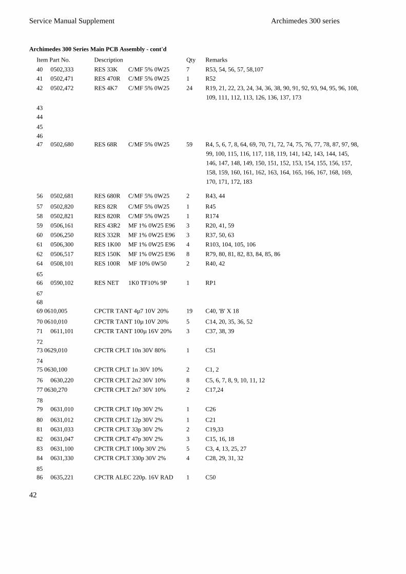
5.1 Parts Lists
Items identified by a * are normally available as spare parts. For details of service and spares policy, see the Acorn Service and Support Strategy document.
Items denoted *+ are available only in sets - see 'Component Sets' at the end of the parts lists.
Archimedes 300Series Packaging Assembly4 0176,003 * Mouse 19 0276,019 * Carton 110 0277,020 * Welcome Disc 111 0276,029 *+ Packaging, Top 112 0276,030*+ Packaging, Bottom 114 0476,000 * Welcome Guide 115 0476,002 * User Guide 116 0476,003 * BASIC/Sprite Editor Keycard 119 0870,353 * Power Lead, 2M Long, c/w 13A Plug 1
Archimedes 300 Series Final Assembly
Item Part No. Description Qty Remarks1 0176,006 * Speaker and LED Assy. 12 0176/008/A Case LowerAssy. 14 0276,002 *+ Front Moulding 15 0276,003 *+ Front Sub-Moulding 16 0276,006 *+ Case Metalwork, Upper 17 0276,015 *+ Front Label, 305 1
0276,315 *+ Front Label, 310 18 0276,017 *+ Base Label 111 0817,005 * Battery, Alkaline 1V5 2AH `AA' 213 0882,655 Screw No. 6 x 1/2" Pan Hd. Pozi AB 2 Item 4 to 214 0882,121 Screw M3 x 6 Pan Hd Pozi 5 Item 6 to 215 0882,654 Screw No. 6 x 3/8" Pan Hd Pozi AB 5 Item 4 to 2/516 0882,949 * Spire Clip No. 6 5 For item 4
Archimedes 300 Series Case Lower Assembly1 0376,340 PCB Assembly (305) 1 Ex ROMS2 0176,002 * 55W 240V PSU 13 0176,004 * 3.5" 1 MB Floppy Disc Drive 14 0176,005 * Single Drive Cable Assy 15 0176,009 * Battery Holder Assy 18 0276,004 *+ Rear Moulding 110 0999,462 *+ Case Metalwork, Lower 111 0276,010 * L.H. Busbar 112 0276,011 * R.H. Busbar 113 0276,012 * Blanking Panel 214 0276,013 *+ Drive Saddle 115 0276,014 * Drive Bracket 116 0276,037 * PCB Side Slide Guide 2 See page 4637 0884,065 * Spacer, Nylon 8mm PCB 1 See page 46
0884,063 * PCB Support Pillar S ee page 4640 0890,009 * Foot Pop-Fit 4mm High 4
40

Archimedes 300 series Service Manual Supplement
Archimedes 300 Series Keyboard Assembly
1 0276,101*+ Keyboard Case Upper 1
2 0276,102 *+ Keyboard Case Lower 1
3 0276,106 *+ Name Case Label 1
4 0276,107 *+ Logo Case Label 1
5 0176,100 * Keyboard PCB Assy. 1 C/W Curly Cable
6 0276,103 * Leg Moulding 1
7 0276,104 * Window Moulding 1
8 0276,105 * Friction Pad 1 For item 7
9 0276,108 * Reset Switch Cap Moulding 1
10 0890,011 * Rubber Foot 4
11 0999,438 * Curly Cable 1 For Keytronics board only
Archimedes 300 Series Main PCB Assembly
ItemPart No. Description Qty Remarks7 0277,022 * 1M Arthur ROM 1 V1.2 1 IC248 0277,023 * 1M Arthur ROM 2 V1.2 1 IC259 0277,024 * 1M Arthur ROM 3 V 1.2 1 IC2610 0277,025 * 1M Arthur ROM 4 V 1.2 1 IC271112 0276,032 * Programmed PAL 16L8A 1 IC44131415 2201,365 * IC ARM 2µm PLSTC 1 IC4316 2201,366 * IC MEMC PLSTC 1 IC4517 2201,367 * IC VIDC 1A PLSTC 1 IC1718 2201,368 * IC IOC PLSTC 1 IC2119202122 0502,100 RES 10R C/MF 5% 0W25 1 R17523 0502,101 RES 100R C/MF 5% 0W25 2 R176,17724 0502,102 RES 1K C/MF 5% 0W25 3 R51,65,6625 0502,103 RES 10K C/MF 5% 0W25 11 R2, 12, 13, 14, 15, 16, 17, 61, 67, 178, 1792627 0502,104 RES 100K C/MF 5% 0W25 2 R73,882829 0502,122 RES 1K2 C/MF 5% 0W25 5 R89, 114, 120, 122, 1383031 0502,181 RES 180R C/MF 5% 0W25 1 R353233 0502,220 RES 22R C/MF 5% 0W25 9 R25-3334 0502,221 RES 220R C/MF 5% 0W25 6 R1, 3, 9, 18, 180, L23536 0502,272 RES 2K7 C/MF 5% 0W25 1 R493738 0502,330 RES 33R C/MF 5% 0W25 2 R181,18239 0502,331 RES 330R C/MF 5% 0W25 3 R60, 123, 129
41
Service Manual Supplement Archimedes 300 series
Archimedes 300 Series Main PCB Assembly - cont'd
Item Part No. Description Qty Remarks
40 0502,333 RES 33K C/MF 5% 0W25 7 R53, 54, 56, 57, 58,107
41 0502,471 RES 470R C/MF 5% 0W25 1 R52
42 0502,472 RES 4K7 C/MF 5% 0W25 24 R19, 21, 22, 23, 24, 34, 36, 38, 90, 91, 92, 93, 94, 95, 96, 108,
109, 111, 112, 113, 126, 136, 137, 173
43
44
45
4647 0502,680 RES 68R C/MF 5% 0W25 59 R4, 5, 6, 7, 8, 64, 69, 70, 71, 72, 74, 75, 76, 77, 78, 87, 97, 98,
99, 100, 115, 116, 117, 118, 119, 141, 142, 143, 144, 145,
146, 147, 148, 149, 150, 151, 152, 153, 154, 155, 156, 157,
158, 159, 160, 161, 162, 163, 164, 165, 166, 167, 168, 169,
170, 171, 172, 183
56 0502,681 RES 680R C/MF 5% 0W25 2 R43, 44
57 0502,820 RES 82R C/MF 5% 0W25 1 R45
58 0502,821 RES 820R C/MF 5% 0W25 1 R174
59 0506,161 RES 43R2 MF 1% 0W25 E96 3 R20, 41, 59
60 0506,250 RES 332R MF 1% 0W25 E96 3 R37, 50, 63
61 0506,300 RES 1K00 MF 1% 0W25 E96 4 R103, 104, 105, 106
62 0506,517 RES 150K MF 1% 0W25 E96 8 R79, 80, 81, 82, 83, 84, 85, 86
64 0508,101 RES 100R MF 10% 0W50 2 R40, 42
65
66 0590,102 RES NET 1K0 TF10% 9P 1 RP1
67
68
69 0610,005 CPCTR TANT 4µ7 10V 20% 19 C40, 'B' X 18
70 0610,010 CPCTR TANT 10µ 10V 20% 5 C14, 20, 35, 36, 52
71 0611,101 CPCTR TANT 100µ 16V 20% 3 C37, 38, 39
7273 0629,010 CPCTR CPLT 10n 30V 80% 1 C51
7475 0630,100 CPCTR CPLT 1n 30V 10% 2 C1, 2
76 0630,220 CPCTR CPLT 2n2 30V 10% 8 C5, 6, 7, 8, 9, 10, 11, 12
77 0630,270 CPCTR CPLT 2n7 30V 10% 2 C17,24
78
79 0631,010 CPCTR CPLT 10p 30V 2% 1 C26
80 0631,012 CPCTR CPLT 12p 30V 2% 1 C21
81 0631,033 CPCTR CPLT 33p 30V 2% 2 C19,33
82 0631,047 CPCTR CPLT 47p 30V 2% 3 C15, 16, 18
83 0631,100 CPCTR CPLT 100p 30V 2% 5 C3, 4, 13, 25, 27
84 0631,330 CPCTR CPLT 330p 30V 2% 4 C28, 29, 31, 32
8586 0635,221 CPCTR ALEC 220p. 16V RAD 1 C50
42

Archimedes 300 series Service Manual Supplement
Archimedes 300 Series Main PCB Assembly - coned
Item Part No. Description Qty Remarks8788 0640,473 CPCTR CER 47n 30V 80% 1 C4989 0650,223 CPCTR MPSTR 22n 50V 20% 2 C22, 239091 0680,002 CPCTR DCPLR 33/47n 0.2" 18 'Z'92 0680,100 CPCTR DCPLR 33/47n AX 12V 39 'A'
96 0701,772 * IC 1772 FDC 28/0.6" 1 IC4798 0704,105 * IC 4464 DRAM 120nS 64Kx4 16 IC69, 70, 71, 72, 73, 74, 75, 76, 78, 79, 80, 81, 82, 83, 84,
85101 0706,552 * IC 65C51 1 IC9102 0708,583 * IC PCF8583 1 IC16103104 0732,630 * IC 26LS30 RS422/423 DRVE 1 IC7105 0732,632 * IC 26LS32 1 IC6106107 0742,005 * IC 74LS05 TTL 14/0.3" 2 IC4, 38108 0742,374 * IC 74LS374 TTL 20/0.3" 1 IC3109110 0744,138 * IC 74ALS138 TTL 16/0.3" 1 IC59111112 0747,000 * IC 74HC00 CMOS 14/0.3" 1 IC46113 0747,004 * IC 74HC04 CMOS 14/0.3" 1 IC15114 0747,014 * IC 74HC14 CMOS 14/0.3" 1 IC20115 0747,075 * IC 74HC75 CMOS 1 IC77116 0747,138 * IC 74HC138 CMOS 16/0.3" 1 IC31117 0747,573 * IC 74HC573 CMOS 20/0.3" 5 IC11, 19, 28, 35, 36118 0747,574 * IC 74HC574 CMOS 2 IC29,30119120 0749,573 * IC 74HCT573 CMOS 20/0.3" 2 IC10,18121122 0770,324 * IC LM423 QUAD OP AMP 1 IC13123 0770,386 * IC LM386 AUDIO AMP 1 IC68
126 0780,239 * TRANS BC239 NPN 2 Q2, 5127 0780,510 * TRANS ZTX510 PNP TO92 1 Q15128 0783,906 * TRANS 2N3906 NP 9 Ql, 3, 4, 6, 7, 8, 10, 12, 13129 0783,904 * TRANS 2N3904 NPN TO92 CBE 2 Q9, 11130 0794,001 * DIODE SI 1N4001 50V 1A 2 D2, 3131 0794,148 * DIODE SI 1N4148 2 Dl, 4
135 0800,004 * CONR 5W SKT DIN RA PCB 1 SK4 (ECONET)136137 0800,050 * CONR 2W WAFR 0.1" ST PCB 2 PL3A138 0800,051 * CONR 3W WAFR 0.1" ST PCB 2 LK2, 6 (NF)139 0800,052 * CONR 5W WAFR 0.1" ST PCB 2 PL2140 0800,070 * CONR 2W SHUNT 0.1" 4 PL3A, LK2, 6
43

Service Manual Supplement Archimedes 300 series
Archimedes 300 Series Main PCB Assembly - cont'd
Item Part No. Description Qty Remarks
141
142 0800,118 * SKT IC 18/0.3" NORM 16 IC51-58 & 60-67
143 0800,120 * SKT IC 20/0.3" NORM 1 IC44
144 0800,131 * SKT IC 32/0.6" NORM 4 IC24, 25, 26, 27
145 0800,169 * SKT IC 68P PLCC 3 IC17, 21, 45
146 0800,185 * SKT IC 84P PLCC 1 IC43
147
148 0800,203 * FSTN TAB 6.3MM X 0.8 ST PCB 4 PL5, 6, 7, 8 (POWER)
153 0800,400 * CONR 64W SKT ST AC PCB SH 1 SK7 (EXPANSION)]
154 0800,458 * CONR 2W WAFR 0,1" ST LK 1 PL11 (BATTERY)
155 0800,459 * CONR WAFR 0.1" ST LK 1 PL9 (FRONT PANEL)
156 0800,481 * CONR 5W HSNG 0.1" PCB 1 SK6 (NET MODULE)
157 0800,484 * CONR 17W SKT HSNG 0.1" PCB 1 SK5 (NET MODULE)
158 0800,611 * CONR PHONO SKT RA PCB 1 SK13
159 0800,642 * CONR 3W 3,5MM RA PCB JSKT 1 SK1 (AUDIO)
160 0800,853 * CONR 2W WAFR 0.156" ST LK 1 PL12 (FAN)
161 0800,919 * SKT 6W MINDIN RA PCB RFI 1 SK12 (KEYBOARD)
163 0803,102 * CONR 34W BOX IDC LP ST 1 SK11 (DISC DATA)168 0820,019 * XTAL 1.8432MHz HC18/U 1 XL1
169 0820,240 * XTAL 24.00 MHz HC18/U 1 XL2
170 0821,327 * XTAL 32.768 kHz CC 0.05" 1 XL3
172 0860,005 * COIL RF 33µH AX Q=45 2 L1, 3
186 0800,291 CONRD 9W PLG RA PCBLK+LK 1 PL1 (SERIAL)
0800,271* CONRD 9W PLG RA PCB+RFI+L OPTION
190 0800,292 CONRD 9W SKT RA PCBLK+LK 1 SK2 (VIDEO)
0800,272* CONRD 9W SKT RA PCB+RFI+L OPTION
194 0800,293 CONRD 25W SKT RA PCBLK+LK 1 SK3 (PRINTER)
0800,273* CONRD 25W SKT RA PCB+RFIL OPTION
0884,044 Rivet, Pop, 3,2D 2 For OPTION items 186, 190, 194
COMPONENT SETS
The following items are available only as sets:
300 SERIES MAIN UNIT 310 Label Set, comprising:Case Metalwork, comprising: 0276,315 310 Case Front Label0276,006 Case Metalwork Upper 0276,017 310 Case Base Label0999,462 Case Metalwork, Lower Packaging Set, comprising:0276,013 Drive Saddle 0276,029 Poly Case Lower0176,009 Battery Holder Assy. 0276,030 Poly Case Upper Case Moulding Set, comprising:0276,002 Front Moulding 300 SERIES KEYBOARD0276,003 Front Sub-Moulding Keyboard Case, comprising:0276,004 Rear Moulding 0276,101 Keyboard Case, Upper305 Label Set, comprising: 0276,102 Keyboard Case, Lower0276,015 305 Case Front Label Keyboard Label Set, comprising:0276,017 305 Case Base Label 0276,106 Name Case Label
0276,107 Logo Case Label
44

Archimedes 300 series Service Manual Supplement
5.2 Production and Field Changes
The following information gives changes and deviations made to the Archimedes 300 series during production and is the latest available when this manual was compiled. It will be updated accordingly as information becomes available.
Main PCBMONO VIDEO OUTPUT
Some issue 2 boards may have a mono video output fault. If other checks do not reveal the cause, check for the presence of insulation tape beneath the RGB video connector SK2 mounting bracket. If no tape is fitted, suspect a short circuit on the mono video track; check for a short circuit to earth (NOT 0v) and, if found, drill out the rivet securing the bracket and place insulation tape underneath the bracket leg toinsulate the track.SOUND OUTPUT FAILUREInsertion of the jack plug into the audio output socket SKT1 causes a temporary short of both audio output devices Q9 and Q11 to OV. If the audio output is not working, check for BC239s fitted at Q9 and Q11. If so, replace them with 2N3904s, Acorn Part Number 0783,904. Note that the 2N3904s have a different pinout to BC239s and have to be fitted in a reversed position - see diagram below. Later boards are fitted with 2N3904s. As these will tolerate the momentary short, they are unlikely to be the cause of audio output failure.
VIEW OF ALTERNATIVE TYPES Q9, Q11 AS SEEN FROM ABOVE.
SERIAL PORT
On issue 1 boards only, two wire links are fitted around ICs 7 and 15, as follows:
IC7 pin 3 and IC15 pin 10 are not inserted into their IC sockets and are connected by a wire link across the top side of the PCB.
The second wire link is fitted between IC7 pins 1 and 4 on the underside of the PCB.
EXCESSIVE BACKGROUND NOISE ON SPEAKER (Acorn FCO E008 refers)
Later boards have a modification to reduce hum from the internal loudspeaker caused by acoustic pick-up.
The modification comprises a 10 V or higher 10 p.F capacitor fitted between pins 7 (+ve) and 4 (-ve) of IC68. The capacitor should be fitted as close as possible to the IC and should be secured to the PCB using glue or hot wax. RS part number 104-449 or 103-957 are suitable capacitors.
Machines in the original serial number range 27-AKB10-1000001 to 27-AKB10-1001277 and 27-AKB15- 1000001 to 27-AKB15-1001752 were not fitted with this modification in production. However, machines outside this range may, on subsequent repair, have been fitted with circuit boards which are not modified.
Note that the noise on earlier computers when BREAK or ESCAPE is pressed is due to a software problem with earlier versions of Arthur, and will be cured when Arthur 1.20 is fitted.
45

Service Manual Supplement Archimedes 300 series
RGB OUTPUT VOLTAGE LEVELS (ACORN FCO E009 REFERS)
The RGB output voltage levels have been raised in production to improve compatibility with certain types of multi-sync monitors. In addition, sync on green is no longer provided. Where problems are experienced with RGB levels being too low for a given monitor, change the values of 0.25W 1% resistors R20, R41 and R59 to 43.20 and remove R39. If 43.20 resistors are not available, 430 1% 0.25W, Farrell part number MRS2543R or RS part number 148-168 may be used as an alternative.
Note: There are problems inherent with removing components from four-layer boards. Components should only be desoldered from the board using vacuum desoldering equipment. An acceptable alternative would be to cut the wires to the components concerned, leaving enough of the wire on the board to allow the new resistor wires to be soldered to them. The new wires should be cropped close to the resistor, but allowing the new solder joint to be effected. On removing R39, which is no longer required, crop the wires back to the board.
VIDEO NOISE (ACORN FCO E011 REFERS)
Breakthrough of system noise occurs onto the screen. This shows as rippling on screen and is particularly noticeable with colour monitors. This seems to be particularly prevalent when running 'Arcwriter'.
If this occurs, solder a 1N4148 diode in parallel with R67 (adjacent to VIDC IC17) with the cathode (dark stripe) at the end nearest Q13. Remove the decoupling capacitor 'A' nearest to 1C17, between it and Q12 either by using desoldering equipment or by cutting the capacitor out, leaving wires long enough to attach a new component. Replace this capacitor with a 22µF 6.3 V or higher axial lead electrolytic capacitor, eg Farnell part number 030 34229. Observe polarity - positive end furthest away from Q12.
PCB MOUNTINGThere have been several methods employed of mounting the main PCB in the case. These include:
i. 8 support pillars, part number 0884,063, fixed to the case. The board rests on these pillars, and is attached to the rear panel.
ii. Later boards are supported by finger grips in the front moulding, with 3 support pillars 0884,063 under the PCB, plus the rear panel. On some units, the 3 support pillars are attached to the board.
iii. The PCB is supported by finger grips in the front moulding and attached to the rear panel. Two PCB slide guides support the board along each side of the case, plus one central nylon spacer, part number 0884,065, attached to the board.
In all instances, exercise extreme care when removing the board from the case, so as not to snag supports or damage the board.
Link 12Link 12 enables selection of ROM device types. The default setting is for EPROMs up to 0.5Mbit, 1Mbit ROMs and 1Mbit non-JEDEC EPROMs. Changing link 12 would allow the use of 1Mbit JEDEC EPROMs.
Issue 1 boards do not have the link fitted.
Issue 2 boards have a link consisting of either four pads or pins and shunts. The tracking is as for an issue 1 board. If the shunts are reversed, this may stop the machine functioning. Tracks need to be cut to change the link.
Phono socket (mono video)Issue 1 boards have a mono video phono connector fitted to the PCB rear panel, with flying leads from the PCB.
Issue 2 boards have a board-mounted socket.
Battery holder
The battery holder is riveted to the base metalwork. If the battery holder is replaced, care must be taken to ensure that the fixing rivets are fitted to the two holes originally used. Only two of the four possible holes hold the battery holder assembly rigid.

Archimedes 300 series Service Manual Supplement
SaddleThe disc drive support 'saddle' is fixed to the base metalwork by either screws or, on later units, rivets. All replacement base metalwork will have a saddle riveted in position.
PSUPower Supply Units manufactured by Sanken have a screw head in the case which may foul the rear panel busbar. If fitting a Sanken PSU as a replacement, it may be necesssary to modify the busbar by filing a piece out of it to clear the screwhead.

Service Manual Supplement Archimedes 300 series

Archimedes 300 series
5.3 HARD DISC PODULE CIRCUIT DIAGRAM

Service Manual Supplement

Archimedes 300 series
5.4 MIDI PODULE CIRCUIT DIAGRAM

Service Manual Supplement

Archimedes 300 series
5.5 ECONET MODULE CIRCUIT DIAGRAM
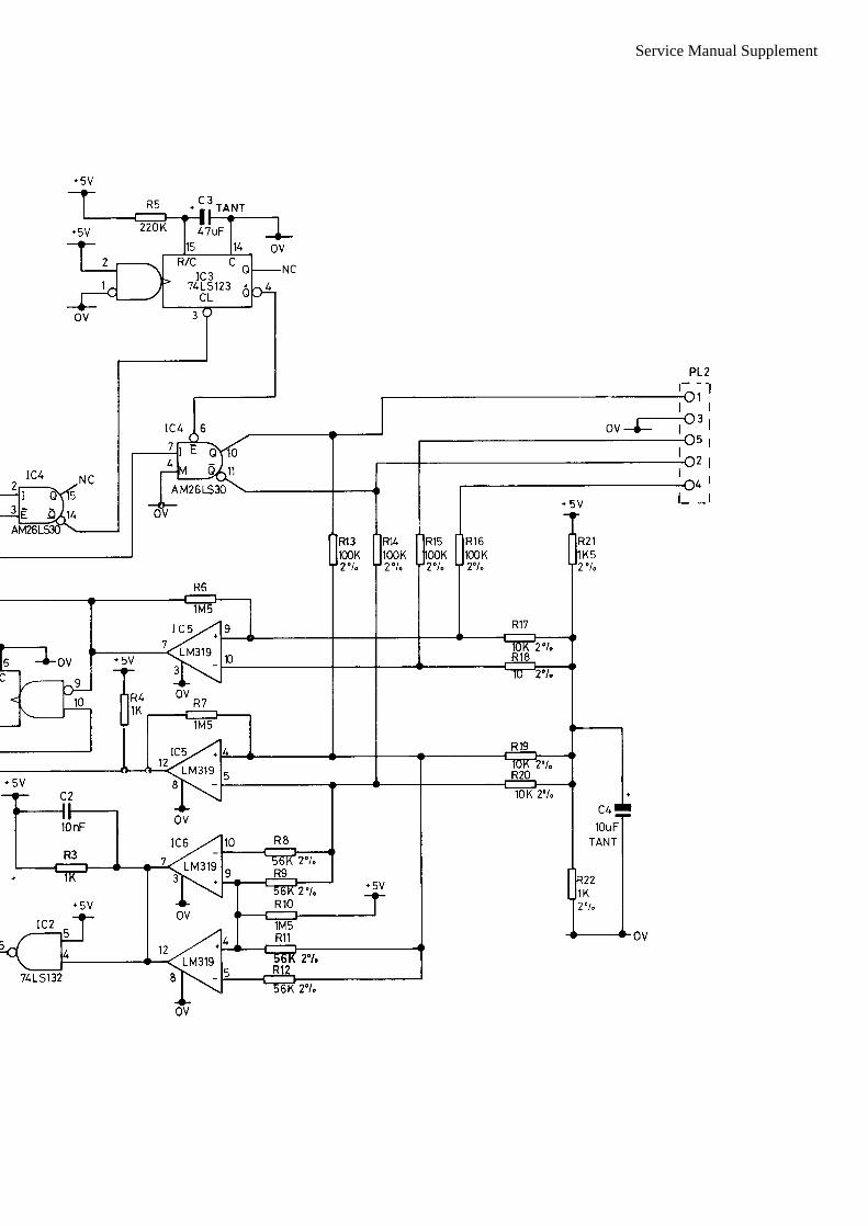
Service Manual Supplement

Archimedes 300 series Service Manual Supplement
5.6 2-WAY BACKPLANE CIRCUIT DIAGRAM