high-level synthesis framework for crosstalk minimization
TRANSCRIPT

University of South FloridaScholar Commons
Graduate Theses and Dissertations Graduate School
10-31-2008
High-Level Synthesis Framework for CrosstalkMinimization in VLSI ASICsHariharan SankaranUniversity of South Florida
Follow this and additional works at: https://scholarcommons.usf.edu/etd
Part of the American Studies Commons
This Dissertation is brought to you for free and open access by the Graduate School at Scholar Commons. It has been accepted for inclusion inGraduate Theses and Dissertations by an authorized administrator of Scholar Commons. For more information, please [email protected].
Scholar Commons CitationSankaran, Hariharan, "High-Level Synthesis Framework for Crosstalk Minimization in VLSI ASICs" (2008). Graduate Theses andDissertations.https://scholarcommons.usf.edu/etd/487
High-Level Synthesis Framework for Crosstalk Minimization in VLSI ASICs
by
Hariharan Sankaran
A dissertation submitted in partial fulfillment
of the requirements for the degree of
Doctor of Philosophy
Department of Computer Science and Engineering
College of Engineering
University of South Florida
Major Professor: Srinivas Katkoori, Ph.D.
Nagarajan Ranganathan, Ph.D.
Hao Zheng, Ph.D.
Sanjukta Bhanja, Ph.D.
Stephen Suen, Ph.D.
Date of Approval:
October 31, 2008
Keywords: Crosstalk noise, Simulated Annealing, Floorplan driven high-level synthesis,
Bus-based design, Macro-cell based design, Coupling parasitics
© Copyright 2008, Hariharan Sankaran

DEDICATION
To the Supreme Providence

ACKNOWLEDGEMENTS
I would like to thank Dr. Katkoori immensely for his guidance, encouragement, and patience
during the entire course of this research. I would like to thank Dr. Ranganathan, Dr. Zheng,
Dr. Bhanja, and Dr. Suen for being on my committee. Acknowledgments to Cadence design
systems, and Dr. James Stine‟s research group in Oklahoma State University for providing 180nm
standard cell library and EDA tools. I take this opportunity to acknowledge the intellectual and
moral support provided by current and past members of the VCAPP group, especially Pradeep and
Vyas. I would also like to acknowledge the help provided by the Computer Science Tech Support
team led by Daniel Prieto. Most importantly, I would like to thank my loving parents Sankaran and
Latha for supporting me right throughout my studies. Finally, a big thank you to my sister Priya,
Hema, Shiva, and rest of my friends and relatives here and back home for supporting me during
different stages of my life to achieve this goal.

NOTE TO READER
The original of this document contains color that is necessary for understanding the data. The
original dissertation is on file with the USF library in Tampa, Florida.
i
TABLE OF CONTENTS
LIST OF TABLES iii
LIST OF FIGURES iv
ABSTRACT viii
CHAPTER 1 INTRODUCTION 1
1.1 On-chip signal crosstalk 2
1.2 ASIC design flow in DSM regime 6
1.3 Need for high-level crosstalk optimization 11
1.4 High-level framework for worst-case crosstalk pattern minimization during
high-level synthesis 15
1.5 Floorplan driven high-level synthesis framework for crosstalk noise
minimization in macro-cell based designs 16
1.6 On-chip dynamic crosstalk pattern detection and elimination technique 17
1.7 Organization of this dissertation 18
CHAPTER 2 BACKGROUND AND RELATED WORK 20
2.1 Crosstalk related terminology and definitions 20
2.2 Effects of crosstalk on reliability of digital circuits 23
2.3 Crosstalk noise estimation models 25
2.3.1 Low level crosstalk noise estimation 25
2.3.2 High-level crosstalk noise estimation 28
2.4 Crosstalk optimization 30
2.4.1 Post-layout crosstalk optimization techniques 30
2.4.2 Routing-level crosstalk optimization techniques 31
2.4.3 Encoding techniques 32
2.4.4 Profile based worst-case crosstalk pattern optimization techniques 37
2.4.5 Unified high-level and physical design synthesis framework 39
2.5 Summary 40
CHAPTER 3 SIMULTANEOUS SCHEDULING, ALLOCATION, BINDING,
RE-ORDERING, AND ENCODING FOR CROSSTALK PATTERN
MINIMIZATION DURING HIGH-LEVEL SYNTHESIS 42
3.1 Motivation 44
3.2 Bus-based interconnect architecture for macro-cell designs 45
3.3 Problem formulation 47
3.3.1 HLS related definitions and terminology 48
3.3.2 Crosstalk optimization 48

ii
3.3.3 Cost function under latency constraints 50
3.3.4 Cost function under resource constraints 50
3.3.5 Cost function under no constraints 51
3.4 Simulated Annealing based crosstalk pattern minimization 51
3.4.1 Simulated Annealing moves 52
3.4.2 Signal generation, DFG profiling, and cost function evaluation 54
3.4.3 Cooling schedule parameters 56
3.5 Experimental results 58
3.5.1 Class I experiments (Bus binding, Re-ordering, and Encoding) 60
3.5.2 Class II and III experiments (Simultaneous exploration of Scheduling,
Allocation, Binding, Re-ordering, and Encoding Subspaces) 61
3.5.3 Comparison with other approaches 69
3.6 Conclusions 71
CHAPTER 4 FLOORPLAN DRIVEN HIGH-LEVEL SYNTHESIS FOR
CROSSTALK NOISE MINIMIZATION IN MACRO-CELL BASED
DESIGNS 74
4.1 Technology characterization for critical bus length calculation 76
4.2 Motivational example 79
4.3 SA framework for floorplan driven HLS to minimize crosstalk violations 82
4.4 Experimental results 85
4.4.1 Experimental setup and flow 85
4.4.2 Results and discussions 88
4.5 Summary 95
CHAPTER 5 ON-CHIP DYNAMIC WORST-CASE CROSSTALK PATTERN
DETECTION AND ELIMINATION FOR BUS-BASED DESIGNS 101
5.1 An illustrative example 102
5.2 Proposed on-chip worst-case crosstalk pattern detection and elimination
technique 105
5.2.1 AUDI design framework 106
5.2.2 Modified RTL design model implementing proposed technique 108
5.3 Experimental results 113
5.4 Conclusions 125
CHAPTER 6 CONCLUSIONS AND FUTURE WORK 126
REFERENCES 129
ABOUT THE AUTHOR End Page

iii
LIST OF TABLES
Table 2.1 Effects of signal transition patterns on coupling capacitances of a victim net
[18] 23
Table 3.1 Experimental setup and purpose of experiments 57
Table 3.2 Data environments 59
Table 3.3 Percentage savings in single data environment 62
Table 3.4 Best case savings under latency constraints (x= multiplier, + = adder,
- = subtractor, B = no. of additional buses, R. P = resource penalty,
S. P = speed penalty) 66
Table 3.5 Best case savings under resource constraints (x= multiplier, + = adder,
- = subtractor, B = no. of additional buses, R. P = resource penalty,
S. P = speed penalty) 67
Table 3.6 Best case savings under no constraints (x= multiplier, + = adder,
- = subtractor, B = no. of additional buses, R. P = resource penalty,
S. P = speed penalty) 68
Table 4.1 Benchmark details 89
Table 4.2 Crosstalk noise violations in proposed framework versus designs synthesized
through traditional HLS flow 91
Table 5.1 Characteristics of different data transmission methods [18] 114
Table 5.2 Bus cycle time calculation based on worst-case propagation delay 116
Table 5.3 Normalized bus cycle time to transmit different coupling signal transition
pattern in DYN and proposed transmission method 119
Table 5.4 Characteristics of designs implementing different crosstalk delay optimization 121
techniques
Table 5.5 Logic overhead 124

iv
LIST OF FIGURES
Figure 1.1 Capacitive and inductive noise peak voltage normalized by Vdd [98] 2
Figure 1.2 Contribution of coupling capacitance in nanometer technology [99] 3
Figure 1.3 First order capacitance model [2] 3
Figure 1.4 Impact of driver sizing (A) Circuit depicting a victim net and aggressor nets (B)
Crosstalk noise effects on a victim net due to driver sizing [5] 5
Figure 1.5 Crosstalk noise computation based on signal timing characteristics [8] 7
Figure 1.6 ASIC design flow [2] 8
Figure 1.7 Proposed high-level frameworks to reduce crosstalk noise violations 14
Figure 1.8 Example of worst-case crosstalk pattern on a 4-bit bus due to temporal
correlation 15
Figure 2.1 Crosstalk noise effects in a two aggressor model 21
Figure 2.2 Crosstalk delay effects on a victim net due to worst-case signal transitions on
victim and aggressor nets 24
Figure 2.3 Crosstalk noise induced functional failure 25
Figure 2.4 Crosstalk noise computation in a charge sharing model [2] 26
Figure 2.5 Circuit modeling an aggressor and victim net to compute crosstalk noise
amplitude [27] 28
Figure 2.6 An example of a victim net coupled to multiple aggressors along its path [27] 29
Figure 2.7 An example of wire perturbation technique to minimize coupling capacitance
between adjacent nets [33] 31
Figure 2.8 Communication model for crosstalk prevention coding technique 33
Figure 2.9 Examples of valid and invalid codeword transitions 34
v
Figure 2.10 Overhead in terms of number of additional bit lines required for encoding
derived based on asymptotic bounds [59] 35
Figure 2.11 Overhead comparison between memoryless encoding and memory based
encoding techniques in terms of number of additional wire requirements [59] 35
Figure 2.12 Implementation details of crosstalk aware variable cycle transmission
method [18] 36
Figure 3.1 Hardware architecture synthesized by AUDI HLS system 46
Figure 3.2 An example floorplan with bus-based interconnect architecture for
macro-cell based EWF design synthesized through Cadence-SOC
Encounter 47
Figure 3.3 Scheduled DFG, a possible bus-based datapath, and an execution trace
for profiling the DFG 55
Figure 3.4 Worst-case crosstalk savings for individual SA moves under Class-I
experimental setup (Experiment 1) 62
Figure 3.5 Average crosstalk savings comparison between Class-I and Class-II
experiments for SIG-1 data environment 64
Figure 3.6 Comparison of percentage of crosstalk free nets for original cost function
versus modified cost function under resource constraints 71
Figure 3.7 Comparison of percentage of crosstalk free nets for original cost function
versus modified cost function under no constraints 72
Figure 3.8 Comparison of percentage of crosstalk free nets for original cost function
versus modified cost function under latency constraints 73
Figure 4.1 Characterization circuit to determine the critical length for crosstalk
noise in 180nm technology node 76
Figure 4.2-A Characterization plot for critical length determination with
inter wire separation = 3 lambda, Vdd=1.8V, technology node = 180nm 77
Figure 4.2-B Characterization plot for critical length determination with inter
wire separation = 6 lambda, Vdd=1.8V, technology node = 180nm 77
Figure 4.2-C Characterization plot for critical length determination with
inter wire separation = 9 lambda, Vdd=1.8V, technology node = 180nm 78
Figure 4.3 Motivational example (A) Scheduled DFG (B) A possible resource and
interconnect binding information for DFG (C) One possible floorplan
for the DFG 80

vi
Figure 4.4 An example of physical synthesis driven HLS to optimize crosstalk
noise in bus-based macro-cell design 81
Figure 4.5 Flow diagram for SA based floorplan driven HLS for crosstalk optimization 83
Figure 4.6 Illustration of bus synthesis and floorplanning step 85
Figure 4.7 Experimental flow 86
Figure 4.8 Crosstalk noise amplitude distributions for multiplexer based point to point
interconnects (Seq. HLS flow) versus bus-based interconnects synthesized
through proposed framework for (A) DCT benchmark and (B) EWF
benchmark 92
Figure 4.9 Crosstalk noise amplitude distributions for multiplexer based point to point
interconnects (Seq. HLS flow) versus bus-based interconnects synthesized
through proposed framework for (A) FFT benchmark and (B) mpeg
benchmark 93
Figure 4.10 Crosstalk noise amplitude distributions for multiplexer based point to point
interconnects (Seq. HLS flow) versus bus-based interconnects synthesized
through proposed framework for ARF benchmark 94
Figure 4.11 Crosstalk optimized bus-based floorplan generated by proposed
floorplan driven HLS for DCT benchmark 96
Figure 4.12 Crosstalk optimized bus-based floorplan generated by proposed
floorplan driven HLS for EWF benchmark 97
Figure 4.13 Crosstalk optimized bus-based floorplan generated by proposed
floorplan driven HLS for FFT benchmark 98
Figure 4.14 Crosstalk optimized bus-based floorplan generated by proposed
floorplan driven HLS for mpeg benchmark 99
Figure 4.15 Crosstalk optimized bus-based floorplan generated by proposed
floorplan driven HLS for ARF benchmark 100
Figure 5.1 (A) Scheduled DFG, (B) A sample execution trace, and (C) A possible
bus-based datapath 103
Figure 5.2 Execution trace on bus B2 for original design versus proposed scheme 104
Figure 5.3 Gate-level circuits for worst-case crosstalk pattern detection 106
Figure 5.4 Proposed crosstalk detection and elimination scheme implementation
on a 4-bit bus 107

vii
Figure 5.5 Typical bus-based interconnect structure generated by AUDI 108
Figure 5.6 Modified architecture implementing proposed crosstalk detection and
elimination technique 109
Figure 5.7 Block diagram for crosstalk detection and crosstalk elimination circuit in
bus-based macro-cell designs 111
Figure 5.8 Crosstalk elimination circuit 112
Figure 5.9 AUDI controller (A) Mealy model based state diagram for DFG shown
in Figure 5.1 (B) Block diagram depicting the RTL model synthesized
by AUDI with proposed crosstalk detection scheme 113
Figure 5.10 Simulation results for IIR filter design implementing the on-chip
crosstalk elimination technique 114
Figure 5.11 Distribution of coupling signal transition pattern for SPEC2000
benchmark suite [18] 117
Figure 5.12 Performance comparison of proposed approach versus other transmission
methods implemented in [18] 118
Figure 5.13 Performance comparisons between DYN and proposed approach to
negate 4Cc and 3Cc signal transition pattern induced delay 120
Figure 5.14 Data pattern distribution based on MCF for HLS benchmarks 122
Figure 5.15 Performance comparison of proposed approach versus other crosstalk delay
reduction techniques 123
Figure 5.16 Percentage of worst-case crosstalk pattern minimized for HLS
benchmarks by proposed SA based framework 125

viii
HIGH-LEVEL SYNTHESIS FRAMEWORK FOR CROSSTALK MINIMIZATION IN
VLSI ASICS
Hariharan Sankaran
ABSTRACT
Capacitive crosstalk noise can affect the delay of a switching signal or induce a glitch on a
static signal causing timing violations or chip failure. Crosstalk noise depends on coupling
parasitics, driver strength, signal timing characteristics, and signal transition patterns. Layout
level crosstalk analysis techniques are generally pessimistic and computationally expensive for
large designs due to lack of design flexibility at lower-levels of design hierarchy. The architectural
decisions such as type of interconnect architecture, number of storage and execution units, network
of communicating units, data bus width, etc., have a major impact on the quality of design
attributes such as area, speed, power, and noise. To address all these concerns, we propose a high-
level synthesis framework to optimize for worst-case crosstalk patterns on coupled nets, a
floorplan driven high-level synthesis framework to minimize coupling capacitance, and an on-chip
technique to dynamically detect and eliminate worst-case crosstalk pattern on bus-based macro-cell
designs.
Due to Miller coupling effect, the switching activity pattern on adjacent nets may increase the
effective capacitance seen by a victim net and thereby it may cause a worst-case signal delay on
the victim net. However, signal activity pattern on coupled nets are dependent on data
correlations which in turn depend on resource sharing. The resource sharing in turn depends on
scheduling, allocation, and binding during high-level synthesis flow. Therefore, we propose a

ix
Simulated Annealing (SA) based design space exploration of HLS design subspace, bus line re-
ordering, and encoding subspaces to optimize for worst-case crosstalk pattern in bus-based macro-
cell designs. We demonstrate that the proposed framework will aid layout level techniques in
eliminating false positive violations. We also propose an SA based algorithm to explore floorplan
and HLS subspaces to optimize coupling capacitances in bus-based macro-cell designs. We have
integrated an RTL floorplanner in HLS flow to estimate coupling capacitances between bus lines.
Crosstalk analysis using Cadence Celtic shows that the designs generated by the proposed
framework results in less number of crosstalk violations compared to designs generated through
traditional ASIC design flow. We also propose an on-chip crosstalk detection and elimination
technique that dynamically detects and eliminates worst-case crosstalk pattern with minimum area
penalty compared to other layout level techniques reported in the literature.

1
CHAPTER 1
INTRODUCTION
Advances in the field of very large scale integrated circuit (VLSI) technology have enabled
integration of circuit components such as transistors, resistors, capacitors, and wires on a very
small scale. According to ITRS07 (International Roadmap for Semiconductors) the projected
feature size of a transistor by 2015 is 10nm [1]. As technology shrinks interconnects which serve
as arteries (or veins) in a digital system are also scaled along lateral dimensions i.e., the wires are
becoming thicker and narrower to reduce the resistance and in turn reduce propagation delay. The
wire spacing also decreases as the technology leaps into ultra deep submicron (UDSM) regimes.
Above 180nm technology nodes circuit parameters such as area, power, and delay used to be
the de facto metrics designers used to focus on while designing VLSI ASICs. For technology
nodes of 180nm or below the designers are forced to consider signal integrity issues during early
stages of the design cycle. Coupling induced crosstalk is considered as the first-order signal
integrity problem in deep submicron (DSM) chips. In DSM regime, the contribution of on-chip
coupling capacitances (or parasitic capacitances) between tall and thin wires in close proximity
account for more than 50% of total wire capacitance [2]. Due to the large on-chip capacitance
between the wires the interconnect delay has become the dominating metric in determining the
performance of a system. Even though the technology is scaled down, the chip area remains the
same (100 mm2 for a standard large chip), and more and more circuit components are packed into
the fixed area, thereby, increasing the interconnect density and associated coupling capacitances
between the closely spaced wires.

2
Figure 1.1. Capacitive and inductive noise peak voltage normalized by Vdd [98]
In this work, we consider only capacitive coupling and ignore inductive coupling. Inductive
crosstalk effects will be more severe for high frequency designs and is difficult to account for at
higher levels of design abstraction. This is so, because the inductance depends on return path of a
current loop which in turn depends on power or ground network which is available only during the
power planning stage of physical design synthesis phase. Figure 1.1 shows the crosstalk noise
effects due to capacitance and inductance for the current technology nodes [98]. As it can be seen,
for advanced technology nodes the impact of capacitive crosstalk effects are more pronounced than
inductive crosstalk. This is due to the fact that as technology shrinks the interconnect spacing is
also reduced which in turn increases the ratio of coupling capacitance to total capacitance as
shown in Figure 1.2.
1.1 On-chip signal crosstalk
On-chip signal crosstalk may cause violation of timing constraints by hastening or delaying the
signal transition or logic failure by inducing a glitch or spurious signal transition on the victim
wire. On-chip crosstalk induced noise is dependent on following parameters:

3
Figure 1.2. Contribution of coupling capacitance in nanometer technology [99]
Figure 1.3. First order capacitance model [2]
Coupling capacitance: In Figure 1.3 the capacitances Ctop and Cbot represent wire-to-
substrate capacitances and Cadj denotes the coupling capacitances between the middle (M)
wire with the wires to its left (L) and right (R). The above configuration is called a first
order coupling capacitance model because coupling capacitances due to immediate
adjacent nets alone are considered. The signal transitions on net L or R or both may
induce a voltage change on net M through charging or discharging of coupling
L M R

4
capacitances (Cadj) between them and thereby, inducing noise on wire M leading to timing
or functional violation on circuits driven by net M. Even though the wires will have some
coupling capacitance with wires that are farther away the effect of these coupling
capacitances are generally minimal. This is so, because coupling capacitances between the
wires decrease with separation distance and thereby reducing their [2].
Driver strength: The signal strength on a net depends on the size of the driver. If a signal
is driven by a large gate then the actively driven net will strongly oppose the signal
transitions from its neighbors thereby, minimizing the impact of coupling capacitance
induced noise. For example, Figure 1.4-A shows the circuit where the victim net (v) is
driven by an inverter and shares coupling capacitance with its immediate neighbors.
Figure 1.4-B shows the crosstalk noise effects on net v driven by inverters inv_4 (i.e.
inv_x represents the minimum width of the transistor multiplied by factor x) and inv_12. It
can be seen that the crosstalk noise at both the receiver input and output of net v is
significantly less for inv_12 compared to that for inv_4. However, sizing up the driver of
victim net may in turn interfere and induce crosstalk noise on its neighbors a_1 and a_2
[4, 5, 6, 96].
Signal transition patterns among the coupled nets: Crosstalk violations depend on data
patterns. In other words, crosstalk depends on temporal correlation between the coupled
signal nets. For example, in Figure 1.3, if the signal on the middle line (M) switches in a
direction opposite to signal transitions on the left (L) and right (R) wires then due to
Miller coupling effect the signal transition on the middle line (M) will be delayed [7].
Miller coupling effect or factor (MCF) describes the effect of signal transition pattern on
coupling capacitances seen by a net. In other words, it describes the multiplicative factor

5
Figure 1.4. Impact of driver sizing (A) Circuit depicting a victim net and aggressor nets
(B) Crosstalk noise effects on a victim net due to driver sizing [5]
(A)
(B)
a_2

6
for coupling capacitances. In the first order coupling capacitance model, the MCF can
vary from 4 to 0 based on the signal transition pattern on coupled nets. For example, in
Figure 1.1 the effect of coupling capacitance seen by M could be as high as 4.Cadj to as
low as zero.
Signal timing characteristics (i.e. slew rate, skew, signal switching time window): Slew
rate is a measure of rate of change of a signal from high to low or low to high. The
difference in switching time between a net and its neighbors is defined as a skew. Signal
timing window represents the duration between the earliest and the latest possible arrival
time of a signal computed during static timing analysis. The signal timing characteristics
such as slew rate and skew determine the amount of delay/speedup is induced on a net
when the adjacent nets are switching in the opposite direction and vice versa [8, 97].
Figure 1.5 shows the signal timing window for both victim (V) and aggressor nets (A1 and
A2). In Case 1, the sweep line intersects A2 and victim (V) timing window. If the sweep
line is pulled from left to right then the sweep line will intersect nets A1 and V timing
windows. However, the sweep line will never intersect both the aggressors (A1 and A2)
and victim (V) timing window. Therefore in Case 1 the impact of crosstalk noise on
victim net will be due to one of the aggressor nets (A1 or A2) and not both. In Case 2, the
sweep line intersects the timing window of all three nets and in this scenario the victim net
will suffer from noise contribution from both the aggressor nets.
1.2 ASIC design flow in DSM regime
Rapid progress in VLSI technology is forcing the designers to constantly evolve the design
flow to meet the power and performance requirements as well as to ensure circuit reliability in

7
Figure 1.5. Crosstalk noise computation based on signal timing characteristics [8]
modern VLSI systems. It also forces the electronic design automation (EDA) community to
develop automated tools to analyze and fix signal integrity issues without any manual intervention.
Figure 1.6 shows the sequence of steps to be followed for designing ASICs in deep submicron
regime [2]. The first step in the design flow is to specify the functional requirements as a
behavioral model. Generally, designers prefer to use Hardware Description Languages (HDL) such
as VHDL or Verilog to capture the behavior of the system followed by functional verification of
the behavioral specification. A commonly employed strategy is to partition a complex system into
modular blocks. Such a strategy allows for logic reuse which in turn helps verification efforts
because it reduces the number of modules that needs to be validated. Design time is also reduced
by allowing multiple groups to work on different modules simultaneously. A good partitioning is
also critical because the quality of design optimization that can be done during high-level synthesis
(HLS) depends on such a partition. High-Level Synthesis (HLS) is the process of automatically
translating a behavioral specification represented as a CDFG (Control Data Flow Graph) into a
A1
V
A2
A1
V
A2
timing window
sweep line

8
Figure 1.6. ASIC design flow [2]
TWF and
Slews
Behavioral
Synthesis
RTL
Logic Synthesis
Gate level
netlist
SPEF
netlist
Static Timing
Analysis
LVS/DRC/ERC
Tapeout
ECOs
System behavior
in HDL
Floorplan
Place & Route
RC Extraction
Crosstalk
Analysis
layout
HDL: Hardware description
language
RTL: Register-transfer level
RC: Resistance and
capacitance
SPEF: Standard parasitic
exchange format
LVS: Layout versus
schematic
DRC: Design rule check
ERC: Electrical rule check
TWF: Timing window file
ECO: Engineering change
order
9
register-transfer level data path (RTL) and a behavioral controller [10]. To accomplish this task a
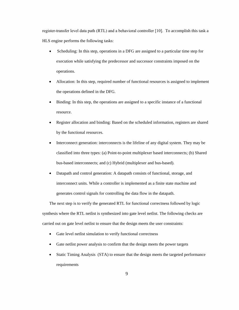
HLS engine performs the following tasks:
Scheduling: In this step, operations in a DFG are assigned to a particular time step for
execution while satisfying the predecessor and successor constraints imposed on the
operations.
Allocation: In this step, required number of functional resources is assigned to implement
the operations defined in the DFG.
Binding: In this step, the operations are assigned to a specific instance of a functional
resource.
Register allocation and binding: Based on the scheduled information, registers are shared
by the functional resources.
Interconnect generation: interconnects is the lifeline of any digital system. They may be
classified into three types: (a) Point-to-point multiplexer based interconnects; (b) Shared
bus-based interconnects; and (c) Hybrid (multiplexer and bus-based).
Datapath and control generation: A datapath consists of functional, storage, and
interconnect units. While a controller is implemented as a finite state machine and
generates control signals for controlling the data flow in the datapath.
The next step is to verify the generated RTL for functional correctness followed by logic
synthesis where the RTL netlist is synthesized into gate level netlist. The following checks are
carried out on gate level netlist to ensure that the design meets the user constraints:
Gate level netlist simulation to verify functional correctness
Gate netlist power analysis to confirm that the design meets the power targets
Static Timing Analysis (STA) to ensure that the design meets the targeted performance
requirements

10
The logic synthesis is followed by floorplanning which determines the relative positions of the
modules based on the connectivity, creation of pad-ring, placement of I/O pads with area
minimization as the primary objective function. Based on the floorplan information packaging
feasibility study is conducted to ensure that the ASIC will confirm to packaging requirements. In
the placement stage, the actual positions for the modules are determined based on the timing/area
requirements followed by power grid construction to meet the power demands of the ASIC.
Routing is carried out next and is generally carried out as a two-step process: (a) Global routing;
and (b) Detailed routing. Global routing determines the regions through which the nets might be
routed. On the other hand, detailed routing determines the exact route between pins of various
communicating modules [11]. After routing, RC extraction is carried out to obtain the SPEF
(Standard Parasitic Extraction Format) netlist containing the extracted coupling capacitances, wire-
to-substrate capacitances, and resistance information for interconnects in the design.
In prior technologies (0.25μm or above) the wire-to-substrate capacitances are more dominant
and coupling capacitances are generally ignored. Therefore, in the design flow only power and
delay analysis were carried out. For technology nodes of 180nm or below, the design engineers
and EDA tool developers are forced to evolve the design flow to incorporate crosstalk analysis to
ensure signal integrity. The next step in the design flow involves running static timing analysis
with extracted SPEF netlist to generate signal timing windows and slew information required for
crosstalk aware delay analysis. Crosstalk induced glitch and delay analysis are carried out to
identify problem noise nets. A problem noise net is a net which may cause functional or timing
violation in a design. Most of the existing techniques and EDA tools attempt to eliminate crosstalk
violations by employing techniques such as wire segment re-arrangement [12], wire re-ordering
[13], wire spacing [14], buffer insertion [15], and shield line insertion [16] to minimize coupling
parasitcs among the interconnects. Once the design passes the crosstalk violation check a series of

11
design checks are performed:
LVS (Layout versus schematic) – LVS check is done to verify whether all the
interconnections in the schematic are exactly replicated in the layout. It also performs
checks to establish physical equivalence such as transistor W/L, and capacitor or resistor
value in the schematic and layout netlist.
DRC (Design rule check) – DRC check is done to verify that a given layout conforms to
the fabrication rules recommended by the vendor for the particular technology node.
Typically DRC checks for geometric and connectivity rules such as width, spacing, layer
connectivity, etc., are carried out.
ERC – Electrical rule check is done to ensure proper electrical connections (i.e., power
and ground connections) by checking for proper contacts in well and substrate to prevent
latch-up effect and electromigration. It also detects electrical faults such as open and short
circuits in the layout.
1.3 Need for high-level crosstalk optimization
Experts both in academia and industry are unanimous in their opinion that crosstalk induced
signal integrity issue is a major design challenge in DSM regime. The current set of EDA tools are
generally built on pessimistic assumptions, thereby, causing them to report too many violations
including significant percentage of false positives. Fixing all such violations is expensive in terms
of design time and chip real estate. From Figure 1.4 it is also clear that the state-of-the-art EDA
tools target eliminating crosstalk violations only during or after routing phase in the design flow.
Such layout level optimization techniques target minimizing coupling capacitance as the only
metric to eliminate crosstalk violations. However as discussed in Section 1.1 crosstalk is a function
12
of not only the coupling capacitance but also driver strength, signal timing characteristics, and
signal transition patterns.
Most of the layout level techniques generally ignore data dependent nature of crosstalk
violations. For example, if two neighboring nets are strongly coupled and are always going to
switch simultaneously in the same direction then the effect of coupling between them will be zero
due to Miller coupling effect. However, layout level analysis and optimization techniques
generally ignore such data dependent nature of crosstalk violations and may flag such nets as
problem noise nets. In addition, layout level crosstalk repair techniques are expensive in terms of
computational time for large designs due to lack of design flexibility at lower levels of design
hierarchy. Design flexibility means the ability to easily modify or explore different solutions in a
short period of time. For example, to insert a shield line on a routed design may require rip and re-
route of several nets. A major disadvantage of layout level crosstalk optimization techniques is that
the majority of design decisions which determine the chip area, interconnections between the
modules, number of interconnects, resource sharing, type of communication architecture, etc., are
taken at higher levels of design abstraction. All these high-level design decisions have a major
impact on the quality of the final layout and by ignoring decisions taken at these levels and
focusing on optimizing crosstalk at the lowest level drastically increases the complexity of
problem. The works proposed in [17] and [18] have shown the impact of these parameters on
meeting the performance constraints in a design. Therefore, we are motivated to explore
techniques at higher levels of design abstraction to eliminate crosstalk violations.
Crosstalk optimization at the higher level of design abstraction has the inherent advantage of
fast design space exploration i.e., it is easier to evaluate the cost of a solution and implement
actions to modify one solution to another. For example, to add an extra functional resource during
allocation phase requires just updating the count for number of instances of that particular resource

13
and evaluating some analytical expression to determine the cost of such a move. On the other
hand, to implement such a move and to evaluate its effect at layout level will be costly because
there might not be enough area to accommodate additional resource without major modifications
to fixed layout. Therefore, we are motivated to explore ways to eliminate crosstalk by developing a
high-level framework that will optimize two primary crosstalk metrics: signal transition patterns,
and coupling capacitance.
A key challenge for crosstalk estimation or optimization at higher level of abstraction is the
non-availability of neighborhood details for interconnects until the routing stage in the design
flow. Therefore, it limits the level at which the crosstalk issues can be handled as evidenced by
multitude of research works during physical design stage of design flow. This scenario is evident
in a point-to-point interconnect architecture where the neighborhood details are known only after
detailed routing. Therefore, crosstalk analysis and repairs can be done only at layout level.
Alternatively, in a bus-based interconnect architecture the neighborhood is partially defined even
before the physical design stage of ASIC design flow. Buses are interconnects shared by various
communicating units thereby reducing the number of connections in a design compared to point-
to-point interconnect architecture. In a bus-based design, key design decisions such as number of
buses, number of bus drivers, type of bus drivers (i.e., multipliers, adders, registers, etc.), and bus
width are made during high-level synthesis. These design decisions have a direct impact on
interconnect structure in final layout. In addition, signal transition pattern on coupled nets are
dependent on data correlations which in turn depend on resource sharing. The resource sharing in
turn depends on scheduling, allocation, and binding during high-level synthesis flow. Therefore,
we propose a high-level framework for reducing the impact of Miller coupling effect (MCF) on
coupled signal nets and a unified high-level and physical synthesis framework for minimizing
coupling capacitance in bus-based macro-cell designs. We also propose an on-chip crosstalk
14
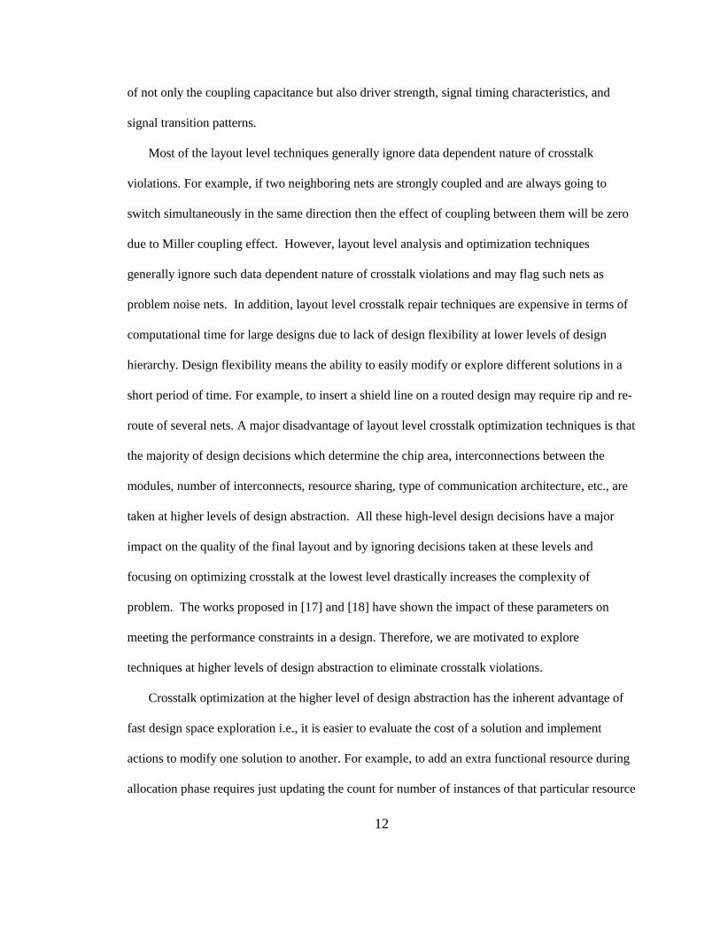
Figure 1.7. Proposed high-level frameworks to reduce crosstalk noise violations
detection and elimination technique to dynamically detect and eliminate the impact of worst-case
crosstalk patterns in bus-based macro-cell designs. Figure 1.7 shows the proposed high-level
framework and on-chip technique to reduce the impact of coupled signal transition patterns and
unified framework to minimize coupling capacitance on bus-based macro-cell designs.
High-level framework
to minimize worst-
case crosstalk pattern
Unified high-level and physical
synthesis framework to minimize
coupling capacitance

15
1.4 High-level framework for worst-case crosstalk pattern minimization during high-level
synthesis
Crosstalk estimation based on pessimistic analysis might report significant number of false
violations. On the other hand, an over optimistic estimator may lead to chip failure. Low level
estimation and optimization techniques are inherently pessimistic in nature because they ignore
data pattern dependent nature of crosstalk violations. Therefore, we propose a high-level synthesis
framework to optimize worst-case signal transition pattern in coupled signal nets. Worst-case
signal transition pattern is also commonly referred to as worst-case crosstalk pattern. Figure 1.8
shows an example of worst-case crosstalk pattern on a 4-bit bus due to temporal correlation. In
Figure 1.8-A the value on bus at time tn-1 is “1101” and “1010” at time tn. Due to temporal
correlation, bit b1 switches in a direction opposite to that of its neighbors thereby inducing a worst-
case delay on b1 due to Miller coupling effect. Similarly, bit b2 in Figure 1.8-B also suffers worst-
case delay.
Figure 1.8. Examples of worst-case crosstalk pattern on a 4-bit bus due to temporal correlation
The proposed approach is as follows: We profile the data flow graph (DFG) for a design by a
typical input sequence and synthesize it to an RTL netlist through our HLS system. We formulate
the problem as simulated annealing based design space exploration problem. We define low
1 1 0 1
1 0 1 0
0 1 0 1
1 0 1 1
b3 b2 b1 b0 b3 b2 b1 b0
tn-1
tn
tn-1
tn
(A) (B)

16
temperature and high temperature moves for each of the HLS tasks (schedule, allocate, and bind)
and a set of crosstalk aware moves implementing bus line re-ordering and data transfer invert
encoding moves. The primary objective is to minimize the number of worst-case crosstalk patterns
with latency (schedule length), and number of functional, storage, and interconnect resource
minimization as secondary goals. Experiments were conducted on DSP benchmarks under latency
constraint, resource constraint, and no constraint environments. The results also show a significant
number of nets (>50%) to be crosstalk free (i.e., nets with zero worst-case coupling transition).
The proposed framework aids the layout level analysis techniques in filtering out false positive
violations. This is so, because layout level analysis tools may flag many of the nets to be noise
nets due to large coupling capacitance between the bus lines under default worst-case scenario
(i.e., the adjacent nets will simultaneously switch in opposite direction). Experimental results show
that upto 75% of nets under resource constraints, 70% of nets under latency constraints, and on
average 55% of nets under resource and latency constraints were found to be crosstalk free i.e.,
they do not require any repairs at layout level even if they are reported as noise nets by pessimistic
crosstalk estimation tool, thereby, eliminating a significant percentage of false positive violations.
Results also show that on average 50% of worst-case signal transitions were optimized over all the
buses in a design under resource and latency constraints.
1.5 Floorplan driven high-level synthesis framework for crosstalk noise minimization in
macro-cell based designs
We have also developed a floorplan driven high-level synthesis tool to produce crosstalk-
immune designs. We formulate the problem as a Simulated Annealing based design space
exploration of HLS and floorplan subspaces to eliminate crosstalk noise violations by optimizing
coupling parasitics in bus-based interconnects. The motivation behind the proposed approach is in
a bus-based communication architecture in which the interconnect resources (buses) are shared by

17
functional (FU) and storage units. A bus is a group of signal wires that run adjacent to each other
connecting various communicating units. The coupling parasitics between the neighboring wires
is proportional to its overlap length. By reducing the length of interconnects (or buses) the
coupling capacitances between the neighboring nets are also reduced, which in turn, reduces
coupling noise on victim nets. The bus length is dependent on the relative locations of
communicating modules in a floorplan and module interconnections from HLS binding phase. It
is also well known that scheduling and allocation have direct impact on HLS binding decisions.
Therefore, we have proposed a framework to simultaneously explore HLS design subspace and
floorplan subspace to optimize crosstalk noise. To validate the proposed approach, the synthesized
RTL designs (with an associated floorplan) are placed and routed by Cadence-SOC Encounter.
Cadence Fire & Ice, a parasitic extraction tool, is used to extract the coupling parasitics and the
crosstalk analysis is performed with Cadence Celtic, a layout level coupling noise analysis tool
employing static noise analysis technique. Experimental results for five benchmarks (DCT, EWF,
FFT, mpeg-motion vector function, and ARF) demonstrate that the proposed approach can reduce
crosstalk violations by as much as 96% (in 180 nm technology node) with an average reduction of
89% over the designs synthesized with traditional sequential flow with 10% area penalty.
1.6 On-chip dynamic crosstalk pattern detection and elimination technique
We present an on-chip crosstalk pattern detection and elimination circuit to eliminate worst-
case coupling transition pattern. ASIC designs are generally synchronous systems. So, in a bus-
based interconnect architecture the bus cycle time has to be set based on the propagation delay of
worst-case crosstalk pattern. However, designs based on such pessimistic estimate are not
desirable because not all the signal transitions might result in worst-case propagation delay and
will adversely impact the performance of the system. We propose an on-chip worst-case crosstalk

18
pattern detection and elimination circuit which dynamically detects and eliminates the worst-case
crosstalk pattern. A worst-case crosstalk happens due to temporal correlation between the data
transmitted on a bus in the previous clock cycle and the data to be transmitted in the current cycle.
The proposed technique eliminates worst-case crosstalk by postponing the transmission of data
pattern which might cause worst-case delay by one clock cycle and instead transmits a logic zero
value on the bus during the current clock cycle. This allows the design to operate at higher clock
frequency and suffers a penalty of one clock cycle only when a worst-case crosstalk pattern occurs.
The proposed technique and SA based worst-case crosstalk pattern minimization framework
complement each other very well. Because SA based HLS framework generates an RTL netlist
optimized for worst-case crosstalk pattern. By implementing the dynamic on-chip technique on
such designs significantly reduces the speed penalty (i.e., one clock cycle per detection) incurred to
eliminate worst-case crosstalk pattern. Similarly, the proposed technique enhances the robustness
of SA based framework as the proposed high-level framework optimizes designs based on input
data profiles. In real time, if the input data trace has different characteristics compared to the input
data profile then it may cause crosstalk violations on buses. In such a case, the proposed technique
provides an additional layer of security by dynamically filtering out such violations.
1.7 Organization of this dissertation
The rest of the dissertation is organized as follows:
Chapter 2 defines basic crosstalk related terminology and notations used in this
dissertation. It also presents a literature survey on crosstalk estimation and optimization at
different levels of design abstraction.
Chapter 3 proposes the high-level synthesis framework for worst-case crosstalk pattern
minimization in VLSI ASICs. A hardware architecture model generated by the framework

19
is presented. We present details on Simulated Annealing based design space exploration
of high-level synthesis, re-ordering and encoding subspace to minimize worst-case
crosstalk pattern.
Chapter 4 presents floorplan driven high-level synthesis framework for minimizing
crosstalk noise by optimizing coupling parasitics. This chapter discusses the need for tight
integration between high-level synthesis and physical design synthesis. We show the
impact of high-level and low level decisions on crosstalk noise metric for bus-based
macro-cell designs. This chapter discusses physical design procedure for generating a bus-
based macro-cell designs using commercial Place & Route tool. We present an
experimental flow for crosstalk analysis using Cadence Celtic crosstalk analyzer. The flow
helps to demonstrate that the designs synthesized by the proposed framework have less
crosstalk violations than that of the designs by the traditional ASIC design flow.
Chapter 5 proposes a dynamic on-chip crosstalk detection and elimination scheme to
eliminate worst-case crosstalk pattern. We present results to show how the proposed
scheme and SA based framework for crosstalk pattern minimization complements each
other well. This chapter demonstrates the effectiveness of proposed scheme over shielding,
double spacing, and encoding approaches.
Chapter 6 draws conclusions and provides directions for the future work.

20
CHAPTER 2
BACKGROUND AND RELATED WORK
Aggressive scaling and dense packing of interconnects in modern VLSI integrated circuits
have exacerbated signal integrity problems. Such problems arising due to on-chip crosstalk
between neighboring wires become more pronounced at deep sub-micron regime. Recently, on-
chip signal crosstalk due to coupling capacitances have become the focus of the research for nano-
scale designs. In Section 2.1, we first present the crosstalk related terminology that will be used
throughout this dissertation. Section 2.2 discusses the effects of crosstalk on circuit reliability.
Section 2.3 surveys the works proposed for crosstalk estimation. Section 2.4 discusses the
techniques proposed to optimize crosstalk at various levels of design hierarchy. Section 2.5
outlines the Simulated Annealing based optimization algorithm and its applications to solve CAD
related problems.
2.1 Crosstalk related terminology and definitions
We first define crosstalk related terminology that is widely used in the literature as well as in
this dissertation.
Victim net and aggressor net: A victim net is a net whose signal can be influenced by the
neighboring nets. A net which influences the signal transitions of its neighbors is an
aggressor net. Technically speaking, every net acts as an aggressor and/or victim.

21
Figure 2.1. Crosstalk noise effects in a two aggressor model
Two aggressor model: A model in which a victim net has two aggressor nets (one on each
side) as shown in Figure 2.1. Each net is driven by and drives a standard inverter load. Vp
is the noise voltage induced due to coupling capacitances as measured on the victim
signal.
Crosstalk pattern and Miller coupling factor: A set of signal transitions on victim and
aggressor(s) that will affect the timing or induce glitch on victim net is generally referred
to as crosstalk pattern. In a two aggressor model, the aggressors and a victim are
represented as (A2, V, A1). The effective capacitance of victim net (V) according to
Miller coupling factor (MCF) is represented as [2, 74, 75]:
E
A2Vc
E
A1Vcgeff
ΔΔCΔΔCCC (2.1)
where ΔV is the voltage change on victim wire and ΔA1 and ΔA2 are voltage changes
on aggressor nets. E represents the supply voltage. Cc and Cg denotes the coupling
capacitances between the victim and aggressor nets and wire to substrate capacitance.
Miller coupling factor describes the factor by which the coupling capacitances will be
multiplied based on signal transition pattern on coupled nets. Table 2.1 shows Miller
coupling effect due to different switching patterns in a two aggressor model. The terms
A
1
A
2
V d
d
Cg
Cg
Cg
Cg
Cc
Cc
Cc
Cc
in Vp
L

22
signal transition pattern and coupled signal transition pattern are also used frequently to
refer to crosstalk patterns.
Example 1: Consider both the aggressors in Figure 2.1 are switching from 0 to 1and
the victim net is switching from 1 to 0. The effective capacitance seen by the victim
net (V) for the supply voltage E = 5V is:
ΔV = 5 – 0 = 5V
ΔA1 = 0 – 5 = -5V
ΔA2 = 0 – 5 = -5V
substituting values of E, ΔV, ΔA1,and ΔA2 in Equation 2.1 we get,
c g5
c5
cgeff 4CC)5(5
C)5(5
CCC
Example 2: Consider only one aggressor A1 in Figure 2.1 is switching from
0 to 1 and the other aggressor net A2 is idle at logic „0‟ (i.e., there is no
switching). The victim net is switching from 1 to 0. In this scenario, the effective
capacitance seen by the victim net for the supply voltage E = 5V is:
ΔV = 5 – 0 = 5V
ΔA1 = 0 – 5 = -5V
ΔA2 = 0 – 0 = 0V
substituting values of E, ΔV, ΔA1,and ΔA2 in Equation 2.1 we get,
c g5
c5
cgeff 3CC)0(5
C)5(5
CCC
Worst-case Crosstalk Pattern: In a two aggressor model, a worst-case crosstalk pattern
refers to the signal transition pattern that causes a worst-case propagation delay on a net.
This happens when the signals on both the aggressor nets switch in a direction opposite to
that of the victim net as shown in Table 2.1 for which the Miller coupling factor is 4 [7],

23
18] . Therefore, the effective capacitance (Ceff) of a victim net will be equal to Cg + 4Cc
and this will lead to worst-case propagation delay on victim net. The signal transitions „↑‟,
„↓‟, and „-„ represents signal transition from logic „0‟ to logic „1‟, logic „1‟ to logic „0‟,
and no transition.
Table 2.1. Effects of signal transition patterns on coupling capacitances of a victim net [18]
2.2 Effects of crosstalk on reliability of digital circuits
The on-chip signal crosstalk may cause two types of failure based on the signal transition
pattern:
Timing Failure (Setup or Hold time violations)
Functional Failure
The propagation delay of a signal is dependent on the resistance and capacitances of the wire
in addition to gate delay. For a circuit shown in Figure 2.1 the total load capacitance seen by the
driving gate is sum of vertical capacitances (Cg) and lateral or coupling capacitances (Cc). The
coupling capacitance (Cc) is determined based on parameters such as wire length (L), layer type,
wire spacing (d), and thickness. Due to Miller coupling effect, the propagation delay is also
dependent on signal transition patterns on these wires.
Figure 2.2 shows the impact of worst-case crosstalk pattern induced delay on a victim net (V).
In Figure 2.2, Vv1(t) is the voltage waveform on the victim net in the absence of coupling
capacitance and Vv2(t) waveform represents the delay induced due to worst-case crosstalk pattern.
Miller Coupling
Factor
Coupling Transition Patterns
(A2,V,A1)
Referred to as
0 (↑,↑,↑) (↓,↓,↓) No Coupling
1 (-,↑,↑) (-,↓,↓) (↑,↑,-) (↓,↓,-) Cc
2 (-,↑,-) (-,↓,-) (↑,↑,↓) (↑,↓,↓)
(↓,↑,↑)(↓,↓,↑)
2Cc
3 (-,↑,↓) (-,↓,↑)(↑,↓,-)(↓,↑,-) 3 Cc
4 (↑,↓,↑)(↓,↑,↓) 4 Cc

24
Figure 2.2. Crosstalk delay effects on a victim net due to worst-case signal transitions on victim
and aggressor nets
In other words, when both the aggressors switch in the same direction as victim net the total
capacitance is Ceff = Cg i.e., coupling capacitance (Cc = 0) will have no effect on delay. If both the
aggressors switch in the opposite direction to that of victim wire (V) then the worst-case delay is
shown by waveform Vv2. This increase in delay due to aggressors (A1 and A2) can cause a signal
to arrive too late at a flip-flop causing setup time violation.
Figure 2.3 shows an example circuit illustrating the effects of crosstalk induced glitch on a
victim net (V) leading to functionality failures. In the example circuit a victim net is driving a reset
input of a flip-flop. As shown in Figure 2.3 the victim net is static (i.e. remains constant at logic
„0‟ or „1‟) and aggressor nets are switching in the same direction. This might induce a glitch on the
reset line (or victim net) based on the coupling capacitances between the neighboring nets. A
glitch on the reset line is fatal as it can reset the output of the flip-flop leading to functional
failures. Therefore, to tackle the crosstalk induced delay and functional failures requires efficient
crosstalk estimation and optimization techniques.
Delay without
coupling
Impact of noise on
delay in
Vv2(t)
Vv1(t)

25
Figure 2.3. Crosstalk noise induced functional failure
2.3 Crosstalk noise estimation models
Circuit attributes such as power, area, delay, switching activity, and coupling noise can be
estimated and optimized at different levels of design hierarchy. Estimation models at lower levels
of design hierarchy are more accurate but are computationally expensive. On the other hand, high-
level estimation techniques are less accurate but enable the designer to fix any violations at the
earliest possible design stage with more degrees of freedom still available for exploration. Based
on the abstraction level the crosstalk estimation models can be broadly classified into two groups:
Low level crosstalk estimation
High-level crosstalk estimation
2.3.1 Low level crosstalk noise estimation
A very straight-forward and an accurate noise estimation technique is to simulate the entire
circuit using circuit level simulation tools such as SPICE [32]. Such techniques are
computationally expensive and not feasible for designs with millions of transistors. Researchers
have proposed several model reduction techniques to estimate coupling noise [19, 20, 21]. In such
techniques, the circuit is modeled as a noise graph. Then, coupling noise waveform is calculated at
each node in the graph. The calculated noise is then propagated through the graph network and
tests are performed to check for noise stability and sensitivity at every node in the design. The
Q
L
A
1
A
2
V
d
d Rs
t
26
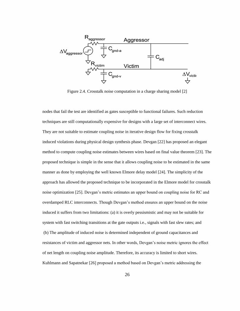
Figure 2.4. Crosstalk noise computation in a charge sharing model [2]
nodes that fail the test are identified as gates susceptible to functional failures. Such reduction
techniques are still computationally expensive for designs with a large set of interconnect wires.
They are not suitable to estimate coupling noise in iterative design flow for fixing crosstalk
induced violations during physical design synthesis phase. Devgan [22] has proposed an elegant
method to compute coupling noise estimates between wires based on final value theorem [23]. The
proposed technique is simple in the sense that it allows coupling noise to be estimated in the same
manner as done by employing the well known Elmore delay model [24]. The simplicity of the
approach has allowed the proposed technique to be incorporated in the Elmore model for crosstalk
noise optimization [25]. Devgan‟s metric estimates an upper bound on coupling noise for RC and
overdamped RLC interconnects. Though Devgan‟s method ensures an upper bound on the noise
induced it suffers from two limitations: (a) it is overly pessismistic and may not be suitable for
system with fast switching transitions at the gate outputs i.e., signals with fast slew rates; and
(b) The amplitude of induced noise is determined independent of ground capacitances and
resistances of victim and aggressor nets. In other words, Devgan‟s noise metric ignores the effect
of net length on coupling noise amplitude. Therefore, its accuracy is limited to short wires.
Kuhlmann and Sapatnekar [26] proposed a method based on Devgan‟s metric addressing the

27
above mentioned limitations. The crosstalk noise is estimated based on a closed form expression
considering the sink capacitances and conductance of victim and aggressor nets.
Another commonly used model to compute the peak noise on a victim net is the charge
sharing model [2]. In this model a circuit is modeled as a capacitive voltage divider to compute the
noise on a victim net. Figure 2.4 shows an example of charge sharing model where the victim net
is actively driven and the driver of the victim net supplies current to oppose the transition or noise
induced by the aggressor net. In such a scenario, the peak noise is dependent on the time constant
ratio k of the aggressor to the victim net. The voltage change on victim net is computed according
to Equation 2.2.
)(
)(k
ΔV k 1
1ΔV aggressor
victim
adjvgndvictim
adjagndaggressor
victim
aggressor
adjvgnd
adj
CCR
CCR
CC
C
(2.2)
Vittal et al. [3, 27] have derived analytical expressions to compute the crosstalk noise
amplitude and noise pulse width based on modifications to charge sharing model. Vittal‟s model
also addresses the combined impact of pulse width and noise amplitude to determine coupling
noise induced violations. It also accounts for drive strengths of victim and aggressor nets.
Equation 2.3 provides the bound on noise pulse amplitude for the circuit shown in the Figure 2.6.
(2.3)
In Figure 2.5, Node O refers to a victim net and node M denotes neighboring aggressor.
Resistance R1 is the driver resistance of aggressor and R2 is the output resistance of victim net.
While C1 and C2 represent wire-to-ground capacitances of aggressor and victim nets respectively
x x C
C
R
R
C
C V p
1
2
1 2 1 1
1
28
Figure 2.5. Circuit modeling an aggressor and victim net to compute crosstalk noise amplitude
[27]
and Cx is the coupling capacitance between the aggressor and victim nets. Vittal‟s model has been
utilized by routers [27] to eliminate the coupling noise induced effects.
The coupling noise introduced by an aggressor net on a victim is calculated using
Equation 2.2. A victim net may have many aggressors along its path as shown in Figure 2.6. Here
the victim net (V) has four aggressor nets and every aggressor may induce crosstalk noise on the
victim net and it may not be possible to evaluate all possible switching combinations to determine
the total coupled noise voltage on a victim. Therefore, superposition theorem is widely used to
calculate the total noise voltage on a victim net. In superposition theorem, the coupling noise due
to each individual aggressor is computed separately assuming all the other aggressor nets are
driven to ground and the total coupling noise is calculated as sum of coupling noise due to
individual aggressors [22, 28, 29].
2.3.2 High-level crosstalk noise estimation
In [30], Gupta and Katkoori have proposed two high-level techniques to estimate the
probability of crosstalk events on the signal lines in a system bus. Due to non-availability of
parameters such as resistance, capacitance, and signal timing characteristics at higher levels of

29
Figure 2.6. An example of a victim net coupled to multiple aggressors along its path [27]
design abstraction, the authors have proposed statistical techniques to estimate crosstalk
probability based on transition patterns on signal nets. In proposed statistical enumerative
approach, they analytically estimate the bit-level crosstalk probability based on word-level
statistical parameters such as mean, standard deviation, and lag-1 temporal correlation. The word
level statistical parameters reflect signal transition pattern on the nets in a design. The time
complexity of statistical enumerative approach is determined to be exponential with respect to bus
width. Therefore, they have proposed an improved statistical non-enumerative approach with
linear time complexity. Experimental results for the statistical estimators have shown that the
proposed high-level estimation technique is reasonably accurate with average errors in the range of
7%-12% when compared against HSPICE simulations for buses ranging from 8 to 32 bits.
Gupta et al. have also proposed a floorplan based crosstalk estimation technique for macro-
cell based designs [31]. In this technique a floorplanner and a global router is integrated with the
statistical estimation flow [30]. The floorplanner determines the relative locations of the modules
and global router provides approximate routes for each net in the design. This information is
utilized by the word-level statistical estimators to estimate the crosstalk probability of a net with
respect to its neighboring aggressor nets. The crosstalk susceptibility information generated by the
statistical engine may then be used to fix crosstalk violations. In [32], Gupta and Katkoori have

30
proposed an optimization technique during behavioral synthesis that searches for crosstalk aware
binding solutions based on the results of high-level statistical estimation models.
2.4 Crosstalk optimization
Over the years, researchers have proposed many crosstalk optimization techniques during the
physical design synthesis phase. Generally, crosstalk optimization is considered to be more
effective at post detailed routing phase. This is so, because coupling parasitics extraction after
detailed routing is more accurate, due to the availability of complete neighborhood details and
dependence on statistical models for coupling capacitance extraction is completely eliminated [34,
35].
2.4.1 Post-layout crosstalk optimization techniques
Some of the most widely implemented post-processing techniques are: changing the wire
spacing between crosstalk sensitive nets, wire re-ordering techniques which attempts to change the
adjacencies among the wires, wire perturbation techniques which attempt to re-arrange wire
segments to influence coupling noise characteristics and gate or transistor sizing techniques.
Figure 2.7 shows an example of impact of wire perturbation in reducing coupling capacitances
between the adjacent wires. Hanchate and Ranganathan [34] have proposed a game-theory based
multimetric optimization approach to optmize crosstalk delay, power, and noise during post
detailed routing phase by determining optimal wire size for the nets. Majority of the above
mentioned postprocessing techniques are geared towards optimizing crosstalk by minimizing
coupling capacitances between the adjacent wires. A major drawback of such post-processing
techniques is it may have very little freedom to explore for new solutions. This is so, because most

31
Figure 2.7. An example of wire perturbation technique to minimize coupling capacitance between
adjacent nets [33]
of the layout is fixed and to rip and re-arrange even few noise sensitive nets may be time
consuming because it may have an adverse impact on its neighbors.
Hanchate and Ranganathan have also proposed a game-theory based post layout gate sizing
technique to simultaneously optimize crosstalk delay and noise [4]. In this work, the authors
attempt to minimize crosstalk by determining optimal drive strength for every net in the design. As
crosstalk noise on a net depends on size of the gates driving the victim net and aggressor net. If the
victim net is driven by a large gate then the current supplied by the gate will be strong enough to
oppose the transitions induced by the aggressors. But the victim net itself will become a dominant
aggressor for its neighbor thereby causing crosstalk violations on the neighbors. The techniques
proposed in [4, 36, 37] attempt to solve the cyclical dependency by determining ideal gate size for
crosstalk sensitive nets.
2.4.2 Routing-level crosstalk optimization techniques
The next high level of design abstraction at which crosstalk optimization is attempted is during
routing phase of physical design synthesis. Generally routing is done as a two step process: Global
routing followed by detailed routing. Crosstalk optimization during detailed routing has more
freedom compared to post layout optimization techniques. Typically the crosstalk-aware routers
start with an initial routing solution and iteratively improve the routing based on the crosstalk

32
constraints. Techniques employed during iterative improvement includes wire segment re-ordering
[33], wire re-arrangement [37, 39], changing track and layer assignments [40, 41], and in some
cases shield insertion [16, 17]. The proponents of optimization during global routing have
pointed out that the routing flexibility to fix violations is limited during detailed routing phase.
This is because during detailed routing the routes of a net are adjusted locally i.e., within a small
routing region thereby the effectiveness of optimization partially depends on global routing
solutions. In global routing, a set of regions in which the wire will go through is determined but
the actual route of the wires and its neighbors are available only during detailed routing phase. So,
optimization during global routing utilizes approximated coupling extraction information to
determine crosstalk sensitive nets [43, 44, 45, 46]. Therefore, considering crosstalk noise
optimization at higher levels comes at the cost of reduced accuracy in estimating coupling
parasitics and noise nets. However, it enhances the range of solutions that can be explored for
crosstalk noise optimization [30, 32]. Researchers have also proposed optimization methods during
the placement stage of physical design synthesis [47, 48].
2.4.3. Encoding techniques
In Section 2.1 we discussed the importance of signal transition patterns and its impact on
crosstalk induced delay and noise due to Miller coupling effect. Research works targeting worst-
case crosstalk pattern elimination implement encoding schemes to prevent coupling transitions on
a victim and aggressor nets that induces maximum delay on a victim net [49, 50]. The motivation
for employing encoding techniques to prevent worst-case coupling transitions is based on the
successful implementation of encoding techniques to optimize dynamic power [51, 52, 53]. There
is a close similarity between optimizing for power and crosstalk in terms of switching activity i.e.,

33
Figure 2.8. Communication model for crosstalk prevention coding technique
to optimize dynamic power, self transition activity on a net has to be reduced and to optimize
crosstalk, coupling transition activity has to be minimized. There are several research works which
try to minimize both self and coupling transitions to achieve low power and crosstalk delay
elimination [54, 55, 56, 57].
The works proposed in the literature that target optimizing worst-case signal transition patterns
can be broadly classified into two types:
Preventive techniques
Reactive techniques
A preventive technique completely eliminates the occurrence of worst-case crosstalk pattern
i.e., the signal on a victim net never switches in a direction opposite to that of its aggressor nets.
Bus encoding techniques [49, 50, 51, 52, 53, 54, 55, 56, 57, 58, 59] proposed in the literature are
examples of preventive techniques. Figure 2.8 shows the communication protocol for encoding
techniques. At the sender side of the bus is an encoder which maps the actual data words to
encoded data generally referred to as codewords before they are transmitted over the bus (or
channel). A codebook defines the mapping between data words to codewords. A fundamental
requirement for all crosstalk prevention coding technique is no two successive codewords can
cause adjacent nets to make transition in opposite direction. Figure 2.9 shows a set of valid and
invalid transitions. A codeword is said to be connected to another codeword if it results in a valid
transition from one to other or viceversa. A neighborset of a codeword is defined as a set of
channel

34
Figure 2.9. Examples of valid and invalid codeword transitions
codewords to which it is connected to and its degree is the size of neighbor set. The authors in [59]
have derived asymptotic bounds on number of additional wires required for different types of
encoding techniques such as memory based encoding (unpruned and pruned) and memoryless
coding techniques.
In unpruned code with memory based encoding technique there is no restriction on codewords
that are allowed in the codebook i.e., all possible n-bit values could be a codeword. The authors in
[59] have proved that the codebook size is at its minimum for class 1 codewords. A class 1
codeword is a codeword with alternating sequence of 0 and 1 bits. For example, 0101 and 1010
are 4-bit class 1 codewords. Figure 2.10 shows the additional bit overhead for unpruned memory
based encoding technique From the figure it is clear that the number of additional bit lines
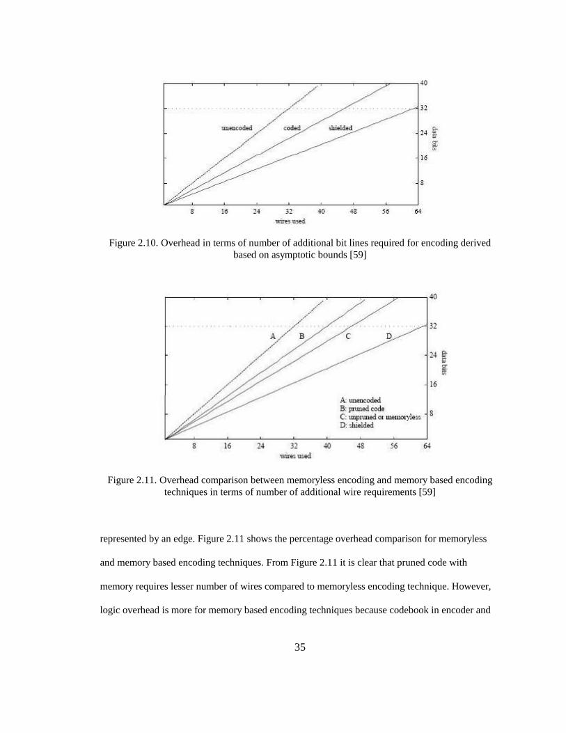
required to encode a 32-bit bus is about 44%. The authors in [59] have also presented a pruning
algorithm to eliminate class 1 codewords from the codebook. Analysis of pruned code with
memory has shown that the wiring overhead could be reduced to 25%.
A memoryless encoding techniques uses a single unchanged codebook i.e., every codeword in
the codebook should be able make a transition to every other codeword defined in the codebook.
The problem of finding largest such codebook is similar to finding the largest clique in a graph,
where each node in a graph represents a codeword and every valid transition between codewords is
Codeword at time (tn-1)
0010
0000
0100
0100
Codeword at time (tn)
0110
1111
0001
0010
valid
valid
valid
invalid
35
Figure 2.10. Overhead in terms of number of additional bit lines required for encoding derived
based on asymptotic bounds [59]
Figure 2.11. Overhead comparison between memoryless encoding and memory based encoding
techniques in terms of number of additional wire requirements [59]
represented by an edge. Figure 2.11 shows the percentage overhead comparison for memoryless
and memory based encoding techniques. From Figure 2.11 it is clear that pruned code with
memory requires lesser number of wires compared to memoryless encoding technique. However,
logic overhead is more for memory based encoding techniques because codebook in encoder and

36
Figure 2.12. Implementation details of crosstalk aware variable cycle transmission method [18]
decoder circuits is dependent on previous value transmitted on the bus. On the other hand,
memoryless encoding has single unchanged codebook.
In a reactive technique, a corrective or counteractive action is taken to nullify the effect of
worst-case crosstalk pattern. Lin, Vijaykrishnan, Kandemir, and Irwin [18] have proposed a
crosstalk aware interconnect technique where data is transmitted at different rates depending on
the data pattern. In their work, a crosstalk analyzer circuit at the sender side of the bus compares
the data to be transmitted in the current cycle with the data transmitted in the previous cycle.
Depending on the type of crosstalk pattern classified according to Miller coupling effect (types of
crosstalk pattern, refer Table 2.1) the number of cycles required to transmit the data is dynamically
determined. Figure 2.12 shows the implementation details of crosstalk aware variable cycle
transmission approach [18].
Generally in a bus-based design the clock cycle time is determined based on worst-case
propagation delay on bus lines, which will be due to worst-case coupled signal transitions (i.e.,

37
MCF =4). However, a major drawback of designing clocks to account for worst-case scenario is it
may drastically affect the performance of the system. In other words, in a design not all signal
transitions will lead to worst-case coupled signal transition and therefore designs with a slower
clock may not provide a performance efficient solution. According to the variable cycle
transmission work, if the current data value causes a worst-case coupled signal transition on a bus
with respect to previous data value, then the data to be transmitted on the bus is kept valid for four
clock cycles to compensate for propagation delay due to crosstalk noise. Similarly, for coupled
signal transitions which causes 3Cc crosstalk patterns and 2Cc crosstalk patterns the data is kept
valid for three and two clock cycles respectively. In addition, the crosstalk analyzer circuit incurs a
latency of one clock cycle to identify the signal transition pattern. The proposed technique incurs
an area overhead of 32% for interconnects of length 2mm and is found to be more attractive for
long interconnects for which the area overhead reduces significantly.
2.4.4 Profile based worst-case crosstalk pattern optimization techniques
Research works that target crosstalk estimation or minimization at higher levels of abstraction
has the advantage of quick design exploration compared to works at lower levels of design
abstraction. The popularity of research works at higher level is quite evident in the case of area,
delay, and power optimization in CMOS circuits [60, 61, 62, 63, 64, 65]. Due to non-availability
of physical level information research works at higher level of design abstraction focus on
minimizing worst-case coupling transition among coupled nets. Lyuh, Kim, et al. [67] have
proposed a bus synthesis algorithm to simultaneously optimize self-transition activity and cross-
talk activity for power minimization given in Equation 2.4 during behavioral synthesis.
Pdyn = (XT. Cs + YT. Cc).Vdd2
(2.4)

38
where Cs and Cc are self and coupling capacitance and Vdd is the supply voltage. XT and YT
represents number of self and coupling transitions for T clock steps. The self transition activity
(XT) is calculated based on number of rising or falling transitions on individual bus lines. On the
other hand coupling transition activity (YT) is calculated based on miller coupling factor between
adjacent lines. The synthesis problem addressed in this work is, given a scheduled DFG and
execution profile for the data transfers; find an optimal assignment of data transfers to buses and
best possible bus-line order to minimize Pdyn defined in Equation 2.4.
The bus synthesis algorithm proposed in [67] has two parts: (a) bus binding algorithm; and (b)
bus line re-ordering algorithm. Lyuh‟s work focuses on minimizing power by incrementally
determining optimal bus binding and bus-line ordering solution at each time step. The authors
have formulated the bus binding problem as a bipartite weighted matching problem (BWMP)
which is optimally solved at each time step through Hungarian method. To determine bus-line
order the authors have formulated the problem as minimum weighted path cover problem
(MPWC). However, MPWC is a NP-complete problem and authors have used a heuristic
algorithm called C-Order to determine bus-line order to minimize coupling transition activity
among neighboring nets. It is well-known that HLS problems are NP-complete and solving for
optimal solution incrementally at each time step may not produce global optimal solution.
E. Naroska, S-J. Ruan et al. [76] have proposed genetic algorithm based multi-level encoding
and wire re-ordering technique to minimize power and crosstalk noise on instruction buses.
According to this approach wires are grouped into pairs and each pair is then encoded through
encoding blocks. The wires could be paired and encoded at multiple levels to further optimize
dynamic power. However, each level of encoding logic introduces additional delay to the datapath.
In order to optimize coupling transition activity an optimal set of wire ordering has to be found.
Since, number of coupling transition also depends on finding optimal set of wire pairing with

39
similar temporal characteristics the authors have proposed genetic algorithm based design
exploration of wire pairing and bus-line re-ordering subspace.
2.4.5 Unified high-level and physical design synthesis framework
Researchers in the past have proposed high-level synthesis framework which takes into
account the cost of interconnects to optimize for area/delay [100, 101, 102, 103]. However,
majority of these works donot consider physical layout information to estimate the cost of
interconnects, instead use simple estimates such as number of interconnects/ multiplexers to
determine the interconnect cost. The popularity of floorplan driven high-level synthesis is quite
evident from number of research works that have been proposed to optimize for area/delay/power
metrics [104, 105, 106, 107, 108]. However, much of the earlier works ignored effects of coupling
transition activity and to the best of author‟s knowledge the unified framework proposed by Zhong
and Jha [66] was the first work to consider cross-coupled capacitance for interconnect power
optimization.
The framework proposed by Zhong and Jha [66] utilizes profiling based technique to
minimize switching activity among interconnects and uses floorplan information to estimate the
wire length and determine effective switched capacitance for every net in the design. From
Equation 2.1 it is clear that the effective capacitance of a net is dependent on both coupling
capacitance and switching patterns among the neighboring nets. Therefore, the authors have
defined two power models: (a) a global power model; and (b) a local power model; to determine
the total power consumption in wires. A global power model is used to determine the wire length
based on RTL floorplan information and a local power model to determine switching capacitance
of a wire based on switching activity of the neighbors. The framework employs an iterative
improvement algorithm which explores HLS and floorplan subspaces to minimize dynamic power

40
consumption in a design. In addition, the framework also includes techniques such as signal gating
with filler values and selection of optimal network topology (i.e., fully dedicated, minimum
spanning tree, trunk-based etc.) to reduce interconnect power due to spurious signal transition on
the datapath units and nets in a design.
2.5 Summary
In this chapter we have presented the following:
Crosstalk related terminology and definitions that will be used in this dissertation
Impact of crosstalk on signal integrity and circuit reliability
Crosstalk estimation models at different levels of design abstraction
Existing research works on optimizing parameters that have direct impact on coupling
noise during different stages of design abstraction.
It is evident from this survey that crosstalk optimization is a complex problem and depends on
multiple parameters such as coupling capacitance, driver strength, signal transition patterns (or
temporal correlation), and signal timing characteristics (i.e. slew rate, skew, and signal switching
time). It also clear that maintaining signal integrity is of paramount importance to ensure circuit
reliability and to meet targeted performance requirements. Existing research works have firmly
established that crosstalk is the biggest signal integrity challenge facing the VLSI designers in the
design of reliable high speed nano-scale VLSI circuits. We also observe that most of the layout
level techniques optimize crosstalk by minimizing coupling capacitance while ignoring the impact
of Miller coupling effect. To address this defect, researchers have proposed several encoding
techniques to eliminate worst-case switching pattern among coupled nets. Recently, researchers
have proposed bus binding techniques to determine optimal bus binding solutions to eliminate
worst-case crosstalk patterns on coupled nets. However, there are very few research works that

41
attempt to optimize crosstalk during behavioral synthesis. The reasons being, lack of enough
physical details to estimate crosstalk noise at higher levels of design abstraction. However, in bus-
based interconnects the interconnect neighborhood is partially defined even before physical design
synthesis phase. In addition, many key architectural decisions that have a direct impact on
interconnects are taken during architecture synthesis phase and high-level optimization also has the
advantage of fast design space exploration compared to layout level techniques. Moreover, a
unified high-level and physical design framework offers the advantage of considering final layout
level effects in high-level decision making process resulting in better optimization of
area/delay/power metrics. Therefore, we are motivated to develop a high-level framework for
crosstalk noise optimization during behavioral synthesis by reducing coupling capacitance and
worst-case switching activity pattern among adjacent nets. To estimate coupling capacitance
requires physical layout level details and switching activity pattern depends on data correlations
which in turn depends on resource sharing. Therefore, we are motivated to explore unified high-
level and physical design synthesis approach to estimate and optimize coupling capacitance. To
influence data correlations on buses we are motivated to explore HLS, encoding, and bus re-
ordering design subspace and also explore the possibility of dynamic crosstalk detection and
elimination schemes to optimize for worst-case coupling transition patterns on on-chip buses.

42
CHAPTER 3
SIMULTANEOUS SCHEDULING, ALLOCATION, BINDING, RE-ORDERING, AND
ENCODING FOR CROSSTALK PATTERN MINIMIZATION DURING HIGH-LEVEL
SYNTHESIS
Crosstalk patterns are dependent on data correlations which in turn depend on resource
sharing. The resource sharing in turn depends on scheduling, allocation, and binding during high-
level synthesis flow. Therefore, we propose simultaneous scheduling, allocation, binding, re-
ordering, and data transfer invert encoding to influence data correlations and generate crosstalk
optimized designs. Compared to a sequential HLS flow, it is well known that simultaneous
exploration of scheduling, allocation, and binding subspaces can produce high quality designs [68,
69, 70, 71, 72, 73].
A key challenge encountered by researchers for tackling crosstalk estimation or optimization at
higher levels of abstraction is the non-availability of physical details (such as track and layer
assignment, wire length, and wire spacing details for all the nets) to estimate coupling parasitics.
The physical details required to estimate coupling parasitics are available only after routing phase.
A bus-based interconnect architecture offers a platform where the adjacent neighbors are clearly
defined even before physical design synthesis. A bus-based interconnect architecture is an ideal
architecture for techniques (such as encoding, reordering, etc.) that target optimizing worst-case
crosstalk pattern and as well as for layout level techniques (such as wire perturbation, wire sizing,
wire separation, layer assignment, shielding etc.) which target minimizing coupling parasitics.
The proposed approach targets worst-case crosstalk pattern minimization in bus-based macro-
cell designs. The proposed technique may not completely eliminate crosstalk in all the buses;

43
however it generates solutions in which several buses are free of crosstalk. Further it identifies bus
lines prone to crosstalk. These details can be utilized by layout level crosstalk optimization tools to
eliminate crosstalk through shield insertion, increased wire spacing, wire perturbation, buffer
insertion, wire sizing etc., on nets identified as crosstalk prone by proposed HLS technique.
The proposed approach is as follows: we profile the data flow graph (DFG) for a design by a
typical input sequence and synthesize it to a RTL netlist through our HLS system. We formulate
the problem as simulated annealing based design space exploration problem. We have defined low
temperature and high temperature moves for each of the HLS tasks (schedule, allocate, and bind)
and a set of crosstalk aware moves implementing bus line re-ordering, and data transfer invert
encoding moves. Experiments were conducted on nine DSP benchmarks under latency constraint,
resource constraint, and no constraint environments. The proposed approach resulted in
minimizing worst-case crosstalk patterns in the range of 29-82% and up to 75% of buses were
found to be immune to crosstalk. The results also show a significant number of nets (>50%) to be
crosstalk free (i.e., nets with zero worst-case coupling transitions).
The main contributions of this work is we propose a SA based simultaneous exploration of
scheduling, allocation, binding, reordering, and data transfer invert encoding design subspaces to
minimize worst-case crosstalk patterns. The proposed framework is best suited for filtering out
false positive violations reported by pessimistic layout level crosstalk analysis tool which ignores
the effects of signal switching pattern and thereby flagging significant number of false violations.
The rest of the chapter is organized as follows: Section 3.1 presents the motivation for the
proposed work. Section 3.2 elaborates on bus-based interconnect architecture for macro-cell
designs. Section 3.3 defines the problem that is to be tackled. Section 3.4 discusses different types
of simulated annealing moves and the proposed worst-case crosstalk pattern optimization

44
framework. Section 3.5 presents and discusses the results for nine DSP benchmark circuits.
Section 3.6 summarizes the proposed approach.
3.1 Motivation
During high-level synthesis, since the physical layout details are not yet defined, it will be
difficult to control the coupling parasitics. However, we can effectively control the crosstalk
patterns. The impact of crosstalk pattern induced delay and techniques for optimizing worst-case
crosstalk transitions have been a hot research topic among the research community [18, 30, 49, 50,
66, 67, 76]. Therefore, we are motivated to explore HLS subtasks such as scheduling, allocation,
and binding to minimize worst-case crosstalk patterns. In addition, we also explore bus line re-
ordering and encoding techniques that affect crosstalk producing switching activity directly. The
data transfer invert encoding move is a simple move with minimum area overhead and is different
from the traditional bus invert encoding proposed by Stan and Burleson [77]. The data transfer
invert encoding inverts the entire data sequence associated with the data transfer. Therefore, the
associated area overhead is for only those data transfers selected for encoding by SA (for each bit-
line of the data transfer, one source inverter, and one inverter for every sink).
During the architecture exploration phase, we can explore different bus binding solutions for
the data transfers. The reasoning behind such an approach is that the data transfers bound to a bus
influences data correlations in bus lines. The data correlations on bus lines can cause worst-case
coupling transitions due to Miller coupling effect. Therefore, exploring for best bus binding
solution can eliminate worst-case coupling transitions on bus lines and prevent crosstalk induced
noise or delay in those bus lines. Simultaneous exploration of scheduling, allocation, and binding
subspaces can vastly increase the range of bus binding solution subspace. In addition to HLS
design space exploration, ordering among bus lines are explored because they directly influence

45
the data correlations which in turn influence worst-case coupling transitions on signal nets (or bus
lines). The motivating factor behind implementing data transfer invert encoding scheme is to
manipulate data correlations among data transfers with minimal area overhead. It is well known
that simulated annealing is a simple and efficient meta-heuristic algorithm capable of finding
global optimal solution in combinatorial optimization problems. It has been widely used in HLS
related problems to minimize power, delay, and area [68, 69, 70, 71, 72, 73, 78].
3.2 Bus-based interconnect architecture for macro-cell designs
For macro-cell designs, the most commonly used interconnect architectures are: (a)
multiplexer based point to point interconnects, and (b) bus-based interconnects. For multiplexer
based designs the net locality details are available only after routing phase. Therefore, for
multiplexer based interconnect designs routing driven or post layout crosstalk optimization
techniques are generally very effective. Most widely employed crosstalk optimization techniques
for multiplexer based point to point interconnects are wire perturbation, layer and track
assignment, wire sizing, and crosstalk driven routing techniques.
In bus-based designs, the adjacent neighbors (left and right neighbors) for each net are clearly
defined. Bus-based interconnects has this inherent advantage of clarity in neighborhood even
before routing phase. Therefore, techniques such as bus-reordering, encoding, bus binding during
HLS, and our proposed work can be employed effectively to control worst-case coupling
transitions which in turn help in minimizing or eliminating crosstalk completely before physical
design synthesis. There are many HLS systems such as Midas [79], CATHEDRAL-II [80], AUDI
(a behavioral synthesis system developed by our research group in USF) [32, 109] etc. that can
generate bus-based interconnect architecture for multi-processor and macro-cell based designs.

46
Figure 3.1. Hardware architecture synthesized by AUDI HLS system
Figure 3.1 shows an example of bus-based interconnect architecture for macro-cell based
designs generated by AUDI HLS system. A synthesized design consists of a datapath and
controller subsystem. A datapath subsystem consists of execution units, storage units, and
interconnects. For bus-based interconnects the bus arbitration logic include sets of tri-state buffers.
Researchers have proposed many bus driven floorplan techniques [81, 82, 83] to generate layouts
for macro-cell designs with bus-based interconnect architecture. Figure 3.2 shows a floorplan for
macro-cell based DCT design with bus-based interconnect architecture generated through
Cadence-SoC Encounter. In macro-cell designs, the hard macros (execution units and storage
units) are routed using lower level metal layers and top two metal layers are generally reserved for
generating bus macros. For example in Figure 3.2 we used layers (metal1-metal3) for routing
C
O
N
T
R
O
L
L
E
R
EXECUTION UNITS
MUL MUL ADD SUB
REG REG REG REG
STORAGE UNITS
DATAPATH
ctrl_signals

47
Figure 3.2. An example floorplan with bus-based interconnect architecture for macro-cell based
EWF design synthesized through Cadence-SOC Encounter
inside the macro-cells (such as execution units and storage units). Metal Layers 4 and 5 were used
for buses. From this discussion, we can conclude that in a bus-based interconnect architecture the
crosstalk related issues such as noise and delay can be addressed effectively by minimizing or
eliminating worst-case crosstalk pattern even before physical design synthesis.
3.3 Problem formulation
We first define few relevant HLS and crosstalk terminology and then formulate the problem
solved in this chapter.

48
3.3.1 HLS related definitions and terminology
Data Flow Graph (DFG) is a graph, G(V, E), such that every vi V, represents a high-level
operation and eij=(vi, vj) E, represents a data transfer from the operation represented by vi to that
of vj.
Timestamp of vi, T(vi) is the time step in which the operation represented by vi is
scheduled to be performed.
Execution Trace of data transfer eij: TR(eij) is the sequence of word values transferred by
eij.
Lifetime of a data transfer eij: T(eij) = [startTije
,endTije
], where startTije
(endTije
) is the time step in
which the data transfer has started (ended). In other words, startTije
= T(vi) and endTije
= T(vj)
where eij=(vi, vj).
Two data transfers eij and epq are compatible if and only if their lifetimes do not overlap
(i.e., they can be bound to same bus) i.e., T(eij) T(epq) = NULL.
Crosstalk event type, Ci, is one of the eight types of worst-case event for the two-aggressor
model.
Crosstalk switching activity of type Ck, X(eij, epq, Ck), due to two data transfers eij and epq is
defined as the total number of Ck events when execution traces of eij and epq i.e., TR(eij)
and TR(epq) are interleaved.
3.3.2 Crosstalk optimization
Given a data flow graph, G, the problem at hand is to perform operation scheduling, resource
allocation, operation and data transfer binding, bus line re-ordering, and data transfer invert
encoding such that the following cost function (О) is minimized:

49
(3.1)
where Ε accounts for crosstalk, Γ for resource utilization, and Δ for speed. Crosstalk event (Ε) is
defined as:
j
jEpqemne kkpqmnWk
,
2
1
)C ,e ,X(e. (3.2)
Wk is the relative weight for the crosstalk events. In this work, Ck is one of the two worst-case
events (↓,↑,↓) and (↑,↓,↑). In other words, we consider crosstalk patterns for which the Miller
coupling factor is 4. The inner summation computes the total cross talk producing activity of type
Ck between the adjacent data transfers emn and epq i.e., emn data transfer occurs before epq data
transfer. The next summation iterates over all data transfers in partition Ej which can be bound to a
single bus. The outermost summation iterates over all partitions (buses).
Γ gives the summation of each type of resource allocated multiplied by relative weight for
each resource type and is defined as:
t
RW tt. (3.3)
t
WW tr (3.4)
Wt is the relative weight for resource type „t‟ and Rt specifies the number of resources allocated for
each resource type „t‟. The relative weight Wt is set proportional to the complexity of the resource
module. For example, an n-bit multiplier carries more weight compared to an n-bit adder or
subtractor module. Δ accounts for performance and is defined as:
ll SW . (3.5)
where Wl is the relative weight for latency and Sl is the length of the schedule.

50
3.3.3 Cost function under latency constraints
The cost function (Оlat) under latency constraints reduces to
normnormlat (3.6)
The crosstalk events (Εnorm), resources (Γnorm) are normalized so that they are in the same scale.
Normalization function is defined as:
maxmaxmax )( *)/( RREEEnorm (3.7)
initEE *2max (3.8)
max/ Rnorm (3.9)
Einit is the cumulative sum of crosstalk events for the initial solution to SA and Rmax is the
maximum number of FU resources needed to implement all the operations and is determined from
ASAP scheduling. The constant factor 2 is determined empirically. E/Emax and Γ/Rmax scales down
the number of crosstalk events (Ε) and resources (Γ) to a real number between 0 and 1. Since the
number of crosstalk events will be in thousands and number of resources will be in tens, a small
increase in number of resources (Γ/Rmax) might dwarf significant decrease in crosstalk events
(E/Emax) in the cost function. So, we scale the crosstalk events to nullify the effect by multiplying
with Rmax in Equation 3.7.
3.3.4 Cost function under resource constraints
The cost function (Оres) under resource constraint environment reduces to
normnormres (3.10)
Similarly normalized crosstalk events (Enorm) and latency (Δnorm) are defined as:
maxmax /*))*2/(( )( initnorm EEE (3.11)
max/norm (3.12)

51
init*5.1max (3.13)
Δinit is the latency of the initial solution. The constant factor 1.5 is determined empirically. We
apply the same reasoning described in the above sub-section (Section 3.2.3) to calculate Enorm
value.
3.3.5 Cost function under no constraints
The cost function (Оnocon) under no constraints reduces to Ε alone. This is accomplished by
setting the weights Wr and Wl to zero and kW to one.
Enocon (3.14)
0;0;1 lrk WWW (3.15)
3.4 Simulated Annealing based crosstalk pattern minimization
Simulated annealing (SA) is a general meta-heuristic for combinatorial optimization capable of
finding global optima and has been explored in the past for HLS [68, 69, 70, 71]. Our main goal
is to simultaneously explore design sub-spaces with scheduling, allocation, binding, and crosstalk
aware moves to synthesize crosstalk optimized design. For large design spaces, SA can be
computationally expensive. In case of HLS problems, even complex DFGs have limited number of
operations constrained by the predecessor/successor relationships. Thus, it is justified to employ
SA for crosstalk activity optimization.
Theoretically speaking, initial solution to SA engine has no bearing on the final solution [84].
Therefore, the initial solution is generated using sequential design flow. All three HLS sub-tasks
combined with re-ordering and invert encoding introduce data correlations. The proposed SA
searches for a solution with correlations that result in less crosstalk.

52
Data Correlations Example: Consider the DFG shown in Figure 3.3 with 4 add and 2
multiply operations. All data transfers are 4 bits wide. Bus B2 carries the output (f) of
operation a2 (at T=2) and is shared by g (at T=3) and out (at T=4). This binding results in
a worst-case crosstalk pattern (on 3 LSBs) because of temporal data correlation on bus B2
during T=2 and T=3. If g is bound to bus B1 then there will be no crosstalk event.
3.4.1 Simulated Annealing moves
Four classes of moves (α, β, γ, and χ) are defined:
Scheduling Moves: explore the temporal space by migrating operations to other valid time
steps.
α1: An operation (say O) and a time step (say T) are selected randomly. O is
migrated to T if and only if O can be executed in T (eg., a3 in Figure 3.3 can be
moved to T=3 resulting in the possibility of e sharing B1 with h provided e and h
are compatible).
Allocation Moves: allocate additional functional resources such as multipliers, adders, etc.,
and busses.
β1: Bus allocate and rebind: A new bus is allocated and a random set of
compatible data transfers are selected and bound to the new bus (eg., In Figure
3.3, add a new bus B4 and bind n and g to B4).
β2: Functional unit allocate and reschedule/rebind: An operation is selected
randomly. Based on the type of selected operation, additional resource is allocated
and bound to the operation (eg., In Figure 3.3, allocate a new adder and move the
operation a1 from time step 1 to 2). Allocate moves directly help scheduling

53
moves (α), and binding moves (γ). Because availability of additional functional
unit allow operations to be re-scheduled at different time steps which in turn
changes the lifetimes of the data transfers resulting in better bus binding
solutions. Similarly, by adding more bus resources results in more freedom for bus
binding moves to explore new solutions.
Binding Moves: help explore the binding solution space.
γ1: Data transfer exchange: two data buses are chosen randomly. For these two
buses, we will determine pairs of swappable data transfers. Then, we randomly
choose a pair and swap them (eg., swap e and f bound to bus B1 and B2 in Figure
3.3.)
γ2: Data transfer migration: We randomly select a bus and then randomly choose
a data transfer. Then, we enumerate all candidate buses to which this data transfer
can be migrated. A random candidate is chosen and the data transfer is migrated.
(eg., In Figure 3.3, migrate g to B1).
Crosstalk Aware Moves: directly affect the crosstalk activity of a bus.
χ1: Bus line reordering: is an effective technique to improve the crosstalk activity,
because the neighboring aggressors for a victim line can be directly influenced.
(In Figure 3.3, eg., re-order the bit lines of B2 ).
χ2: Invert encoding of a data transfer: can effectively reduce the switching
activity at the cost of area/speed overheads. In the context of high-level synthesis,
we explore invert encoding scheme. (For example, invert the data-transfer f. In
Figure 3.3 this move is shown by the redundant pair of inverters (in dashed
boxes). Note that when this move is implemented, the net effect is that bus B2

54
will be shared by the data transfers { f , g}. In other words, the word values
appearing on the bus will be cycled in the order: f and g.)
Note that the invert encoding move that we explore as χ2 move is different from the traditional
bus-invert encoding as proposed by Stan and Burleson [77]. The key difference is that the bus-
invert encoding scheme works on a word value basis i.e., the new word (say y) is compared with
the previous word (say x) on the bus and then y or y is transmitted (which ever results in least
activity). Bus invert encoding incurs area overhead i.e., logic to compute the activity savings
between the new and old values. On the other hand, the χ2 move inverts the entire data sequence
associated with the data transfer. The associated area overhead is as follows: for each bit-line of
the data transfer, one source inverter and one inverter for every sink.
3.4.2 Signal generation, DFG profiling, and cost function evaluation
Auto Regressive Moving Average (ARMA) model was used to generate correlated data
stream. ARMA models are widely used in speech [85] and video coding applications [86]. ARMA
models were also used as statistical signal generation models in the work proposed by Ramprasad,
Shanbag, and Hajj [87]. Gupta and Katkoori [30] have used ARMA statistical model in their intra-
bus crosstalk estimation using word level statistics work. ARMA models are commonly employed
to represent stationary signals and also to represent signals obtained from sources such as speech,
audio, and video [87]. In the proposed work, we use ARMA models to generate correlated data
streams for DSP applications. The DFG is simulated with the input data stream obtained from
ARMA model to generate the execution traces for each data transfer in the DFG. At each
temperature, after the moves have been implemented the cost function Equation 3.1 is evaluated
for the entire data path. For each data bus, the resultant data stream is constructed by using the bus

55
Figure 3.3. Scheduled DFG, a possible bus-based datapath, and an execution trace for profiling the DFG
+
b
e
a
a1
+
c d
f *
g
m2
T=1
T=2
T=3
T=0
a2
*
h
k
+
a3
j
n
m
1
ADD1
B1 B2
B3
MULT1
a
c
b
d
e
f
e f
g
j k
ADD2
n n
h
d
Execution Trace:
a = 0001, b = 0001, c = 0011, d = 0010
e = a + b = 0010
f = c + d = 0101
g = e * f = 1010
Bus Binding:
B1: {e}
B2: {f, g, out}
B3: {n, h}
FU Res Binding:
MULT-1: {m1, m2}
ADD-1: {a1, a2,
a3, a4}
+ T=4
out
a4

56
binding information as well as the execution traces associated with the data transfers. The
following example illustrates the crosstalk activity computation for a bus.
Example: Bus B2 in Figure 3.3 is bound with three data transfers, namely, f, g, and out
and the respective sources are add operation a2, multiply operation m2, and a4. The
sequence of bus writes is: a2 → m2 → a4 → a2, which follows from the scheduled time
stamps of the source operations. If f0, f1, f2,… is the data stream of f, g0, g1, g2,… is that
of g, and out0, out1, out2 … of out then the resulting data sequence on B2 is f0, g0, out0,
f1, g1, out1, f2, g2, out2…□
3.4.3 Cooling schedule parameters
Initial temperature (T0): of SA cooling schedule is a temperature where exp(-ΔCij/T0) ≈ 1
(in other words virtually all the transitions are accepted), where ΔCij is the cost change
from move i to move j. Researchers have proposed many ways to empirically determine
the initial temperature [84]. We used the following equation to determine the initial
temperature:
)( 1
00
ln
CT (3.16)
where ΔC+ is the average cost of uphill move and X0 is the acceptance ratio. From
Equation 3.16 T0 is determined to be 1000 for FIR and FFT benchmarks and for DCT and
EWF benchmarks, T0 is found to be 2000.
Stop criterion: The stop criterion is specified by the number of consecutive SA moves for
which the solution remains the same (in other words, the solution has converged). In this
work, we empirically set the limit to 60.

57
Cooling rate: The annealing schedule is given by:
Tn = λn T0 0.0 < λ < 1.0 (3.17)
Where λ is known as the “cooling rate” and is set to 0.95, Tn is the temperature in the nth
iteration.
Table 3.1. Experimental setup and purpose of experiments
Experimental Setup
Type of experiments
Purpose of
experiments
CLASS I
Bus binding (γ) and
Crosstalk aware moves (χ)
to minimize frequency of
worst-case coupling
transitions
(Original cost function)
Experiment 1
(only one set of move is
enabled)
Effectiveness of
individual SA
moves
(bus binding (γ) and
crosstalk aware
moves (χ))
Experiment 2
(simultaneous
exploration of γ and χ )
Best case savings
for bus binding (γ)
and crosstalk aware
moves (χ)
CLASS II
Scheduling (α), Allocation
(β), Binding (γ), and
Crosstalk aware moves (χ)
to minimize frequency of
worst-case coupling
transitions
(Original cost function)
Experiment 3
(simultaneous
exploration of HLS, re-
ordering, and encoding)
Best case savings
under latency
constraints
Experiment 4
(simultaneous
exploration of HLS, re-
ordering, and encoding)
Best case savings
under resource
constraints
CLASS III
Scheduling (α), Allocation
(β), Binding (γ), and
Crosstalk aware moves (χ)
to maximize number of
crosstalk free nets
(Modified cost function)
Experiment 5
(simultaneous
exploration of HLS, re-
ordering, and encoding)
Best case savings
under no constraints
(resource or latency)
Experiment 6
(simultaneous
exploration of HLS, re-
ordering, and encoding)
To test the
effectiveness of cost
function to
minimize frequency
of worst-case
transitions and
maximize number of
crosstalk free nets
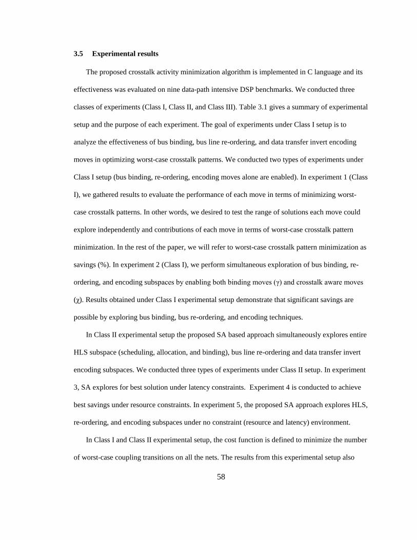
58
3.5 Experimental results
The proposed crosstalk activity minimization algorithm is implemented in C language and its
effectiveness was evaluated on nine data-path intensive DSP benchmarks. We conducted three
classes of experiments (Class I, Class II, and Class III). Table 3.1 gives a summary of experimental
setup and the purpose of each experiment. The goal of experiments under Class I setup is to
analyze the effectiveness of bus binding, bus line re-ordering, and data transfer invert encoding
moves in optimizing worst-case crosstalk patterns. We conducted two types of experiments under
Class I setup (bus binding, re-ordering, encoding moves alone are enabled). In experiment 1 (Class
I), we gathered results to evaluate the performance of each move in terms of minimizing worst-
case crosstalk patterns. In other words, we desired to test the range of solutions each move could
explore independently and contributions of each move in terms of worst-case crosstalk pattern
minimization. In the rest of the paper, we will refer to worst-case crosstalk pattern minimization as
savings (%). In experiment 2 (Class I), we perform simultaneous exploration of bus binding, re-
ordering, and encoding subspaces by enabling both binding moves (γ) and crosstalk aware moves
(χ). Results obtained under Class I experimental setup demonstrate that significant savings are
possible by exploring bus binding, bus re-ordering, and encoding techniques.
In Class II experimental setup the proposed SA based approach simultaneously explores entire
HLS subspace (scheduling, allocation, and binding), bus line re-ordering and data transfer invert
encoding subspaces. We conducted three types of experiments under Class II setup. In experiment
3, SA explores for best solution under latency constraints. Experiment 4 is conducted to achieve
best savings under resource constraints. In experiment 5, the proposed SA approach explores HLS,
re-ordering, and encoding subspaces under no constraint (resource and latency) environment.
In Class I and Class II experimental setup, the cost function is defined to minimize the number
of worst-case coupling transitions on all the nets. The results from this experimental setup also

59
show that a significant number of nets are crosstalk free. In other words, a crosstalk free net is
defined as a net with zero worst-case coupling transitions. This raise a question about our cost
function definition, i.e., is it better to define a cost function to maximize number of crosstalk free
nets instead of minimizing the frequency of worst-case patterns. Thus, in Class III experimental
setup we modified the cost function to account for number of crosstalk free nets and collected
results under no constraint, latency constraint, and resource constraint environment.
The input signals for the experiments are generated based on the ARMA equation.
x(n) = µx γ(n) + σx + ρx x(n − 1) (3.18)
where μx, σx, and ρx are the word-level statistical parameters, namely, mean, standard
deviation, and temporal correlation coefficient. Equation 3.18 is a first order ARMA model as the
value of signal x(n) is dependent only on its prior value. This temporal dependence is modeled as
temporal correlation coefficient (ρx). The noise term γ(n) is discrete and has a standard normal
distribution. By varying these parameters, different data streams can be generated. Temporal
dependence of the signal x(n) on its previous value can be varied by temporal correlation
coefficient (ρx). Table 3.2 lists the correlated signals generated using first order ARMA equation.
The generated signal values are represented in 16-bit or 32-bit binary 2‟s complement
representation.
Table 3.2. Data environments
Signal Environment ARMA Equation
SIG-1 2γ(n) + 40 + 0.35 x(n − 1)
SIG-2 γ(n) + 29 + 0.27 x(n − 1)
SIG-3 1.3γ(n) + 18 + 0.6 x(n − 1)
The experiments were conducted on five different test sets generated from the same signal
environment as the profile data set. We generated 6 correlated data streams of length 1000 vectors
for every data environment (refer Table 3.2). One data stream is used to profile the DFG and five

60
data streams are used as test sequences. The DFG is scheduled using force directed scheduling
algorithm. For every operation type minimum number of resources are allocated and bound by
employing greedy allocation and binding algorithm that minimizes the functional unit area. Based
on the lifetime of the data transfers they are partitioned and bound to buses using left edge
algorithm. The solution thus obtained is used as an initial solution by simulated annealing
algorithm. The savings reported for each experiment is obtained by comparing crosstalk optimized
final solution with the initial solution.
3.5.1 Class I experiments (Bus binding, Re-ordering, and Encoding)
The number of worst-case crosstalk patterns in a bus is dependent on data correlations which
in turn is dependent on bus binding solutions. Therefore, we first conducted experiments to
ascertain the individual impact of bus binding, re-ordering, and data transfer invert encoding
moves. Figure 3.4 shows the results obtained for individual SA moves on different benchmarks.
Figure 3.4 compares the contributions on nine benchmarks to evaluate the effectiveness of binding
moves (γ), individual crosstalk aware moves such as bus line reordering and invert encoding of
data transfer, and combination of crosstalk aware moves (χ). From Figure 3.4 we can make the
following observations: (a) reordering move is the most effective move; (b) re-ordering combined
with inversion is even better; (c) the binding moves and inversion moves by themselves are less
effective in the case of FIR filter. This can be explained by the fact that FIR filter has limited
concurrency; therefore, limited opportunities for bus binding space exploration; (d) In the case of
DCT, FFT, and EWF the binding move is reasonably effective.
We conducted another set of experiment to analyze the effectiveness of simultaneous exploration
of bus binding, re-ordering, and data transfer invert encoding moves and its impact on savings (% of
worst-case crosstalk pattern reduction). Table 3.3 shows the results obtained for nine benchmarks for a

61
single data environment (SIG-1). ARMA signal generation model was used to generate six different
data streams from the same signal model. From Table 3.3, we can observe that in general the
simultaneous exploration of binding, re-ordering, and encoding can yield greater savings.
3.5.2 Class II and III experiments (Simultaneous exploration of Scheduling, Allocation,
Binding, Re-ordering, and Encoding Subspaces)
In Class II experimental setup we perform simultaneous exploration of scheduling, allocation,
binding, re-ordering, and encoding subspaces. Since number of time steps required to execute a
task and number of available functional resources are critical factors in determining the
concurrency, simultaneous exploration of HLS subspace may produce optimal bus binding
solution and a superior design compared to that produced by a sequential flow. We conducted
three experiments to evaluate the proposed approach.
Experiment 3 analyzes the crosstalk minimization under latency constraints.
Experiment 4 measures the savings under resource constraint.
Experiment 5 measures crosstalk minimization in an unconstrained environment.
The experiments were conducted on 16-tap FIR (low-pass, high-pass, and band-pass), 32-tap
FIR (low-pass, high-pass, and band-pass), 8-point DCT, 8-point FFT, and 5th order elliptic wave
filter benchmarks. FIR filters were designed in MATLAB according to required filter
specifications (low-pass, high-pass, and band-pass). The filter coefficients generated for specific
filter specification along with the correlated data stream generated by ARMA model were used to
profile the DFG. In case of DCT and FFT benchmarks constants, twiddle factors, and correlated
data were used to profile the DFG. We selected 8-point DCT and FFT benchmarks because they
are widely used in multimedia applications. The proposed approach is implemented as a part of,
AUDI, our behavioral synthesis system. The HLS benchmarks are synthesized on 2048MB Sun
Ultra dual processor workstation with processor speed of 450MHz.

62
Figure 3.4. Worst-case crosstalk savings for individual SA moves under Class-I experimental setup
(Experiment 1)
Table 3.3. Percentage savings in single data environment
Benchmarks
Savings (%)
Test1 Test2 Test3 Test4 Test5
FIR-16 (LP) 45.83 43.59 44.11 43.10 43.49
FIR-32 (LP) 38.22 39.62 39.98 39.04 38.51
FIR-16 (HP) 51.08 48.94 48.06 50.24 48.63
FIR-32 (HP) 46.11 47.07 47.56 46.33 46.28
FIR-16 (BP) 54.97 55.01 53.03 54.40 55.24
FIR-32 (BP) 52.03 51.23 50.35 50.40 52.51
DCT 36.20 36.66 36.39 36.31 35.16
FFT 59.34 62.17 61.31 61.89 61.50
EWF 32.01 30.86 30.23 31.22 31.35

63
Tables 3.4, 3.5, and 3.6 tabulate the results obtained. The description of columns in each table
is as follows. Column 1 reports the design and the complexity (number of taps and filter order).
Column 2 lists the data environments. Columns 3-7 report the crosstalk savings. Columns 8-9
report the additional number of resources and control time steps utilized by final crosstalk
optimized design compared to initial solution generated through traditional HLS flow. Column 10
reports the percentage of buses on which the worst-case coupling transitions are eliminated
completely. While column 11 reports the number of nets (%) in a design with zero worst-case
transitions. Column 12 reports the number of inverters required for implementing data transfer
invert encoding scheme.
Experiment 3 under latency constraints: Table 3.4 shows the results for experiment 3
under latency constraints. The objective of this experiment is to determine the best case
savings achievable under user defined latency constraint with minimum resource penalty.
We can make the following observations: (a) the crosstalk reduction is in the range of
37%-73% (FFT benchmark provides as high as 73%); (b) the percentage of buses for
which no ground shielding is required ranges from 12-60%; (c) FIR and EWF benchmarks
do not result in any bus that is entirely crosstalk free. But, a significant number of lines (or
nets) within a bus are found to be crosstalk free (i.e., zero worst-case coupling
transitions) as shown in column 11; (d) For all the benchmarks a significant number of
nets (> 50%) are found to be crosstalk free thereby reducing the number of shield line
requirements by more than half; and (e) Column 12 reports the number of inverters
required to accomplish the data transfer invert encoding scheme.
Experiment 4 under resource constraints: Table 3.5 shows the results obtained under
resource constraints for the nine DSP benchmarks. The following observations could be
made from Table 3.5: (a) for FFT design, comparing with Table 3.4 it can be that

64
observed for S2 and S3 the savings under resource constraints is 2-7% more than the
savings under latency constraints; (b) DCT under latency constraints produces marginally
better savings compared to savings under resource constraints; (c) for FIR filter savings
under resource constraints and latency constraints are approximately same except for
FIR-16 High pass filter, savings as high as 65% are obtained compared to 58% under
latency constraints; (d) FFT benchmark under latency constraints gave better results for
percentage of buses with zero crosstalk producing events. While for DCT benchmark the
difference is minimal; and (e) it is clearly evident that a significant number of nets are
crosstalk free under both latency and resource constraint environment.
0
10
20
30
40
50
60
70
80
90
FIR-16 LP
FIR-32 LP
FIR-16 HP
FIR-32 HP
FIR-16 BP
FIR-32 BP
DCT FFT EWF
Cros
stal
k Sa
ving
s (%
)
Benchmarks
Exp-2
Exp-3
Exp-4
Exp-5
Figure 3.5. Average crosstalk savings comparison between Class-I and Class-II experiments for
SIG-1 data environment

65
Experiment 5 under no constraints: This experiment is conducted to evaluate the savings
under no latency and resource constraint environment. The SA approach is given full
freedom to explore complete HLS solution subspace. From Table 3.6 we make the
following observations: (a) FFT benchmark produced savings as high as 84% compared to
73% achieved under resource and latency constrained environment; (b) percentage of
buses without any crosstalk producing events is better for FFT benchmark under no
constraints compared to results with constraints; (c) as expected the savings under no
constraint are better compared to those with resource or latency constraints; (d) savings as
high as 86% of crosstalk free nets is obtained under no constraint environment; and (e)
comparing the results for experiments 3 and 4 versus experiment 5 clearly demonstrates
that significant savings could be obtained under resource or latency constraints.
Figure 3.5 compares the average worst-case crosstalk savings of Class-I and Class-II
experiments for SIG-1 data environment. It is clearly evident from Figure 3.5 that Class II (i.e.,
Exp-3, Exp-4, and Exp-5) experiments results in better savings than Class-I experiment (Exp-2).
Because under Class-I experimental setup, SA explores bus-binding, re-ordering, and inversion
design subspace. While in Class-II experiments, SA also explores scheduling and allocation sub-
spaces to produce crosstalk optimized designs. The average execution time for each of the
benchmark is under 12 minutes (this includes profiling, SA run, and crosstalk computation for 5
test cases).
Experiment 6 - Comparison with Modified Cost Function: We modified the cost function
described in Section 3.2.2 to target number of crosstalk free nets rather than reducing the
frequency of worst-case coupling transitions in all the nets in a design. In other words, SA
explores design space to produce a design in which majority of nets are crosstalk free i.e.,
the number of worst-case transitions in those nets will be zero.

66
Table 3.4. Best case savings under latency constraints (x= multiplier, + = adder, - = subtractor, B = no. of additional buses, R. P = resource
penalty, S. P = speed penalty)
Benchmarks
Data
Env
Savings (%) Worst-case alone Res.Usage
Details
x,+,-,B
%
Speed
Penalty
% Buses with no
crosstalk
producing events
% nets with no
crosstalk
producing events
No. of
inverters
Test1 Test2 Test3 Test4 Test5
FIR-16
(LP)
SIG-1
SIG-2
SIG-3
50.29
39.28
49.88
49.15
38.77
49.34
48.71
38.26
51.87
48.68
38.01
50.54
49.00
38.57
51.56
2,1,0,1
1,2,0,1
2,1,0,1
0
0
0
0
0
0
51.8
49.4
54.1
255
306
340
FIR-32
(LP)
SIG-1
SIG-2
SIG-3
42.23
48.56
55.06
42.16
48.38
55.42
41.60
48.90
58.63
42.46
49.50
55.23
41.02
49.51
57.63
2,0,0,1
2,0,0,1
1,1,0,1
0
0
0
0
0
0
49.4
50.6
56.5
391
442
476
FIR-16
(HP)
SIG-1
SIG-2
SIG-3
52.81
47.29
57.14
52.79
45.20
56.90
51.74
43.79
58.32
53.30
43.44
57.05
52.49
43.13
58.20
1,1,0,1
1,1,0,1
2,1,0,1
0
0
0
0
0
0
56.4
54.1
57.6
340
289
221
FIR-32
(HP)
SIG-1
SIG-2
SIG-3
56.27
48.54
49.02
56.75
49.02
50.65
55.03
47.45
49.97
56.91
47.86
49.14
56.55
49.41
50.83
2,1,0,1
1,3,0,1
2,3,0,1
0
0
0
0
0
0
50.6
51.8
51.8
425
442
391
FIR-16
(BP)
SIG-1
SIG-2
SIG-3
57.82
45.34
44.93
58.17
44.09
47.82
59.62
41.75
46.83
58.13
43.91
44.92
57.02
43.26
43.29
2,2,0,1
2,1,0,1
1,1,0,1
0
0
0
0
0
0
54.1
50.6
55.3
391
340
442
FIR-32
(BP)
SIG-1
SIG-2
SIG-3
55.17
41.12
47.15
53.28
42.35
49.98
53.97
42.65
49.03
53.39
42.47
47.38
54.18
43.37
50.11
1,1,0,1
2,2,0,1
2,4,0,1
0
0
0
0
0
0
49.1
49.1
50.6
442
408
493
DCT
SIG-1
SIG-2
SIG-3
40.55
32.53
41.14
41.40
35.07
37.60
40.17
34.66
36.90
39.96
35.25
37.80
38.48
33.12
35.79
1,0,2,4
2,0,1,4
1,0,1,4
0
0
0
33.33
12.50
16.7
52.7
48.0
55.3
352
240
264
FFT
SIG-1
SIG-2
SIG-3
72.30
64.67
69.15
73.52
65.37
68.31
72.68
65.07
66.36
73.28
65.30
66.61
72.66
65.96
67.86
0,0,1,4
1,3,4,4
1,1,1,3
0
0
0
60.0
45.0
52.63
69.3
63.2
70.9
288
208
176
EWF
SIG-1
SIG-2
SIG-3
37.51
36.18
42.07
36.87
35.44
41.44
36.87
35.76
41.93
36.82
37.67
40.80
37.68
35.78
41.69
0,2,0,4
1,2,0,4
2,1,0,4
0
0
0
0
0
0
47.5
48.1
53.8
432
312
384

67
Table 3.5. Best case savings under resource constraints (x= multiplier, + = adder, - = subtractor, B = no. of additional buses, R. P = resource
penalty, S. P = speed penalty)
Benchmarks
Data
Env
Savings (%) Worst-case alone Res.Usage
Details
x,+,-, L
%
Speed
penalty
% Buses with no
crosstalk
producing events
% nets with no
crosstalk
producing events
No. of
inverters
Test1 Test2 Test3 Test4 Test5
FIR-16
(LP)
SIG-1
SIG-2
SIG-3
47.87
39.98
48.43
47.03
37.62
49.67
46.51
38.01
49.29
47.39
37.86
50.01
48.14
37.73
50.17
0,0,0,5
0,0,0,3
0,0,0,4
29.4
17.6
23.5
0
0
0
52.9
51.8
51.8
272
306
306
FIR-32
(LP)
SIG-1
SIG-2
SIG-3
42.11
45.31
51.13
41.59
45.93
51.42
40.07
44.68
48.94
39.54
45.00
52.42
39.19
45.85
53.27
0,0,0,6
0,0,0,6
0,0,0,5
17.6
17.6
14.7
0
0
0
50.6
54.1
54.1
340
425
442
FIR-16
(HP)
SIG-1
SIG-2
SIG-3
59.28
51.62
64.38
56.57
51.63
64.13
56.01
51.03
65.24
59.38
50.45
63.99
57.54
50.19
65.07
0,0,0,6
0,0,0,2
0,0,0,4
35.2
11.8
23.5
0
0
0
58.8
50.6
60.0
374
306
272
FIR-32
(HP)
SIG-1
SIG-2
SIG-3
54.09
49.15
50.32
54.31
49.73
50.06
53.76
48.31
49.83
54.62
49.97
48.61
54.91
49.92
50.85
0,0,0,4
0,0,0,6
0,0,0,5
11.7
17.6
14.7
0
0
0
50.6
57.6
55.3
391
425
391
FIR-16
(BP)
SIG-1
SIG-2
SIG-3
55.81
44.25
44.42
56.26
44.41
44.53
57.55
43.86
44.72
56.89
43.19
43.27
56.13
44.52
43.11
0,0,0,4
0,0,0,4
0,0,0,5
23.5
23.5
29.4
0
0
0
54.1
50.6
51.8
357
323
408
FIR-32
(BP)
SIG-1
SIG-2
SIG-3
57.30
43.19
50.12
57.92
45.34
49.74
56.66
43.72
49.87
56.17
43.98
49.92
56.81
43.61
49.04
0,0,0,5
0,0,0,5
0,0,0,6
14.7
14.7
17.6
0
0
0
48.2
51.8
50.6
408
425
442
DCT
SIG-1
SIG-2
SIG-3
39.71
31.71
39.97
37.66
32.97
39.77
35.49
29.26
38.60
37.13
32.52
37.11
34.39
31.57
37.98
0,0,0,4
0,0,0,6
0,0,0,4
23.5
35.2
23.5
25
16.7
12.5
51.2
53.8
50.6
376
216
312
FFT
SIG-1
SIG-2
SIG-3
72.20
72.60
70.71
73.38
73.24
69.16
72.94
72.71
67.77
73.49
72.29
68.14
72.19
73.02
68.67
0,0,0,2
0,0,0,2
0,0,0,4
13.33
13.33
26.66
42.1
40.0
52.63
68.1
69.7
76.3
272
256
192
EWF
SIG-1
SIG-2
SIG-3
38.72
34.25
42.05
37.32
33.65
43.09
37.82
34.59
41.38
38.36
35.89
43.36
38.78
33.81
41.62
0,0,0,1
0,0,0,2
0,0,0,2
6.2
12.4
12.4
0
0
0
47.1
49.2
53.2
360
336
336

68
Table 3.6. Best case savings under no constraints (x= multiplier, + = adder, - = subtractor, B = no. of additional buses, R. P = resource
penalty, S. P = speed penalty)
Benchmarks
Data
Env
Savings (%) Worst-case alone Res.Usage
Details
x,+,-,B,L
%
Speed
penalty
% Buses with no
crosstalk
producing events
% nets with no
crosstalk
producing events
No. of
inverters
Test1 Test2 Test3 Test4 Test5
FIR-16
(LP)
SIG-1
SIG-2
SIG-3
55.63
45.32
58.55
53.91
44.01
58.14
53.45
42.77
57.69
54.79
43.83
58.93
56.12
45.17
59.10
2,1,0,1,3
2,2,0,1,3
3,1,0,1,3
17.6
17.6
17.6
0
0
0
54.1
52.9
52.9
221
323
323
FIR-32
(LP)
SIG-1
SIG-2
SIG-3
46.80
49.18
62.52
44.78
48.88
61.31
44.63
50.56
62.90
46.43
49.40
61.73
45.28
49.06
62.58
2,1,0,1,4
3,1,0,1,2
2,1,0,1,1
11.7
5.8
2.9
0
0
0
50.6
51.8
55.3
442
496
510
FIR-16
(HP)
SIG-1
SIG-2
SIG-3
63.43
54.77
59.21
60.18
51.43
57.70
62.10
51.79
58.91
61.79
51.30
57.26
60.66
51.99
59.72
3,1,0,1,4
2,1,0,1,2
2,1,0,1,3
23.5
11.7
17.6
0
0
0
61.3
57.5
58.8
306
323
221
FIR-32
(HP)
SIG-1
SIG-2
SIG-3
67.05
52.52
51.65
66.43
53.46
51.54
65.05
53.10
52.03
66.71
54.25
49.72
65.58
52.24
52.76
2,1,0,1,2
2,1,0,1,2
2,1,0,1,4
11.7
5.8
11.7
0
0
0
56.5
57.6
60.0
425
442
391
FIR-16
(BP)
SIG-1
SIG-2
SIG-3
68.36
53.28
57.84
67.07
52.80
57.08
65.06
53.26
58.64
64.77
53.26
55.60
66.79
52.79
56.59
1,2,0,1,3
2,1,0,1,2
2,1,0,1,3
23.4
11.7
17.6
0
0
0
60.0
58.8
55.3
408
357
425
FIR-32
(BP)
SIG-1
SIG-2
SIG-3
64.01
52.64
55.35
63.78
53.17
53.52
61.71
52.65
53.48
63.20
54.23
56.30
63.37
53.70
53.04
2,1,0,1,4
2,2,0,1,3
2,2,0,1,3
11.7
8.8
8.8
0
0
0
49.1
52.9
52.9
442
476
527
DCT
SIG-1
SIG-2
SIG-3
42.53
33.91
43.21
41.69
32.51
41.43
44.73
36.25
45.12
43.26
34.72
43.93
41.25
35.35
42.56
2,3,3,4,3
1,3,4,4,3
1,2,3,4 ,3
17.6
17.6
17.6
8.3
16.7
16.7
57.2
58.0
64.0
352
272
288
FFT
SIG-1
SIG-2
SIG-3
84.05
75.41
75.44
84.46
75.77
74.07
84.31
75.21
73.17
84.02
75.29
72.90
84.09
75.82
74.54
1,1,0,4,3
2,3,4,4,2
2,1,0,4 ,2
20
13.3
13.3
75.0
50.0
57.14
81.3
79.5
86.3
256
208
192
EWF
SIG-1
SIG-2
SIG-3
41.73
37.03
44.58
40.54
36.85
43.74
40.45
36.77
44.25
41.17
38.76
43.46
40.58
37.50
44.19
1,2,0,3,2
1,1,0,3,1
2,1,0,4,1
12.4
6.2
6.2
0
0
0
48.4
51.1
56.4
312
384
432

69
A possible by-product of exploration with modified cost function is it may increase the
frequency of worst-case transitions in other nets. The problem at hand is to minimize the
cost function (Оmod):
mod (3.19)
where η accounts for number of crosstalk sensitive nets, Γ for resource utilization, and Δ
for latency measured in terms of control steps. Figure 3.7 shows the percentage of
crosstalk nets for designs generated using original cost function (O) and modified cost
function (Omod) under no constraint (resource or latency) environment. It is very interesting
to see that the percentage of crosstalk free nets for original and modified cost function are
approximately the same. In some cases the original cost function produces marginally
better results in terms of percentage of crosstalk free nets compared to modified cost
function. This clearly shows that the cost function to minimize the frequency of worst-case
coupling transitions (original cost function) in all the nets also generates designs in which
a significant percentage of nets are entirely crosstalk free. This experiment clearly justifies
the effectiveness of our original cost function defined to minimize the frequency of
number of worst-case coupling transitions. Figure 3.6 and 3.8 also shows the percentage
of crosstalk free nets between original versus modified cost function under latency and
resource constraints are approximately equal.
3.5.3 Comparison with other approaches
To the best of author‟s knowledge the work proposed by Lyuh, Kim, and Kim [67] is the only
approach that tries to minimize crosstalk activity during high-level synthesis. The primary goal of
their approach is to simultaneously minimize self transition and coupled transition activities to
optimize power. They have proposed a bus binding and bus line reordering algorithm to minimize

70
worst-case transitions. They have formulated the bus binding problem as a bipartite weighted
matching problem which is solved optimally at each time step through Hungarian method. The bus
line re-ordering problem is solved through a heuristic algorithm (C-Order).
We could not quantitatively compare our results with that of work proposed in [67] due to the
fact the authors did not report resource/latency details for the benchmarks, and as well as
percentage of savings for worst-case coupling transitions alone through their proposed bus
synthesis algorithm. While qualitative comparison between the two approaches suggests solving
or finding optimal bus binding solution at each time step might result in sub-optimal solution
which is the case with the work in [67]. On the other hand, we have formulated the problem as SA
based design space exploration where we simultaneously explore HLS subspace (scheduling,
allocation, and binding), bus line re-ordering, and encoding subspaces. As it is well known
simulated annealing based exploration has a better probability of finding global optimal solution
compared to heuristic approaches. Another qualitative difference between the two approaches is
the number of resources is fixed in [67] but our proposed approach explores allocation subspace to
find optimal resource requirements.
Shin and Sakurai have proposed a coupling driven bus design for low power [88]. In their
work, they have proposed a heuristic bus line ordering scheme to minimize coupling transitions.
The authors in [88] have compared their heuristic approach with SA based bus line ordering
scheme. The results show SA based bus line ordering produces marginally better results compared
to the proposed heuristic approach in [88]. From Figure 3.4 and Table 3.3 we can see our
proposed SA based bus binding, re-ordering, and encoding scheme clearly results in better savings
compared to SA scheme exploring only bus line ordering subspace. From this discussion, we can
conclude that the proposed approach will clearly result in better savings compared to the heuristic
approach in [88].

71
Figure 3.6. Comparison of percentage of crosstalk free nets for original cost function versus
modified cost function under resource constraints
3.6 Conclusions
In this work, we demonstrate the feasibility of optimizing crosstalk early in the design flow.
Crosstalk is a function of data correlations and physical characteristics. Since we do not have
physical details, we focus on the data correlations. The proposed simultaneous algorithm attempts
to optimize correlations during HLS flow that result in reduced crosstalk for bus-based
interconnect architecture for macro-cell designs. We have also demonstrated that the proposed
algorithm yields significant crosstalk reduction under both resource and latency constraints.
0102030405060708090
100
FIR
-16
(LP
)
FIR
-32
(LP
)
FIR
-16
(H
P)
FIR
-32
(H
P)
FIR
-16
(B
P)
FIR
-32
(B
P)
DC
T
FF
T
EW
F
FIR
-16
(LP
)
FIR
-32
(LP
)
FIR
-16
(H
P)
FIR
-32
(H
P)
FIR
-16
(B
P)
FIR
-32
(B
P)
DC
T
FF
T
EW
F
FIR
-16
(LP
)
FIR
-32
(LP
)
FIR
-16
(H
P)
FIR
-32
(H
P)
FIR
-16
(B
P)
FIR
-32
(B
P)
DC
T
FF
T
EW
F
% o
f C
ross
talk
fre
e n
ets
Benchmarks
Original Cost Function
Modified Cost Function

72
Figure 3.7. Comparison of percentage of crosstalk free nets for original cost function versus modified cost function under no constraints
0
10
20
30
40
50
60
70
80
FIR
-16
(LP
)
FIR
-32
(LP
)
FIR
-16
(HP
)
FIR
-32
(HP
)
FIR
-16
(BP
)
FIR
-32
(BP
)
DC
T
FFT
EWF
FIR
-16
(LP
)
FIR
-32
(LP
)
FIR
-16
(HP
)
FIR
-32
(HP
)
FIR
-16
(BP
)
FIR
-32
(BP
)
DC
T
FFT
EWF
FIR
-16
(LP
)
FIR
-32
(LP
)
FIR
-16
(HP
)
FIR
-32
(HP
)
FIR
-16
(BP
)
FIR
-32
(BP
)
DC
T
FFT
EWF
% o
f cr
oss
talk
fre
e n
ets
Benchmarks
Original Cost Function
Modified Cost Function

73
Figure 3.8. Comparison of percentage of crosstalk free nets for original cost function versus modified cost function under latency
constraints
0
10
20
30
40
50
60
70
80
90
FIR
-16
(L
P)
FIR
-32
(L
P)
FIR
-16
(H
P)
FIR
-32
(H
P)
FIR
-16
(B
P)
FIR
-32
(B
P)
DC
T
FF
T
EW
F
FIR
-16
(L
P)
FIR
-32
(L
P)
FIR
-16
(H
P)
FIR
-32
(H
P)
FIR
-16
(B
P)
FIR
-32
(B
P)
DC
T
FF
T
EW
F
FIR
-16
(L
P)
FIR
-32
(L
P)
FIR
-16
(H
P)
FIR
-32
(H
P)
FIR
-16
(B
P)
FIR
-32
(B
P)
DC
T
FF
T
EW
F
% o
f cr
oss
talk
fre
e n
ets
Benchmarks
Original Cost Function
Modified Cost Function

74
CHAPTER 4
FLOORPLAN DRIVEN HIGH-LEVEL SYNTHESIS FOR CROSSTALK NOISE
MINIMIZATION IN MACRO-CELL BASED DESIGNS
To optimize coupling noise induced delay or glitch during high-level synthesis is challenging
due to lack of enough low-level layout details. Researchers have successfully implemented unified
behavioral and physical design synthesis techniques to minimize interconnect delay and power
[89, 90, 91, 92, 93, 94] in VLSI designs. Pasricha, Dutt, Bozorgzadeh, et al. [17] have proposed
floorplan-aware bus architecture synthesis (FABSYN) to synthesize cost-effective bus-based
communication architectures that satisfy performance constraints in a SOC design. To the best of
our knowledge, the proposed work is the first significant work to employ unified approach to
optimize for crosstalk violations in an ASIC. We also validate the design using industrial crosstalk
analysis tool (Cadence Celtic). In the proposed approach we integrate a high-level synthesis (HLS)
engine and a RTL floorplanner that aids in estimating low-level physical details. Such a floorplan
driven approach can take into account the effect of high-level design (i.e., scheduling, allocation,
and binding) decisions and floorplan decisions to optimize coupling noise and use this information
to synthesize crosstalk optimized RTL design with an associated floorplan. The computational
complexity of such an integrated approach is very less when compared to that of the physical
design tasks (placement, global/detailed routing).
In the proposed approach, we have developed a floorplan driven high-level synthesis tool to
produce crosstalk-immune designs. We formulate the problem as a Simulated Annealing based
design space exploration of HLS and floorplan subspaces. To estimate the coupling noise on

75
signal nets requires neighborhood information for each victim net. This is the case with the bus-
based interconnect architecture for which the neighborhood is clearly defined even before the
global/detailed routing phase. The motivation behind the proposed approach is in a bus-based
communication architecture the interconnect resources (buses) are shared by functional (FU) and
storage units. A bus is a group of signal wires that run adjacent to each other connecting various
communicating units. The coupling parasitics between the neighboring wires is proportional to its
overlap length. On reducing the length of interconnects (or buses) the coupling capacitances
between the neighboring nets are reduced which in turn reduces coupling noise on victim nets.
The bus length is dependent on the relative locations of communicating modules in a floorplan and
module interconnections from HLS binding phase. It is also well known that scheduling and
allocation have direct impact on HLS binding decisions. Therefore, in this work we have
proposed a framework to simultaneously explore HLS design subspace and floorplan subspace to
optimize crosstalk noise. The problem at hand is to optimize the cost function which is a weighted
sum of estimated floorplan area, latency (schedule length), and the number of crosstalk prone
buses. The number of crosstalk prone buses are determined by characterizing the technology node
a priori to determine the critical net length (denoted by Lcrit), which is the minimum bus length
above which the bus may suffer crosstalk noise. The effect of a high-level decision is evaluated by
updating the floorplan and identifying crosstalk prone buses (i.e., those buses exceeding Lcrit).
Based on the computed cost, SA moves are employed to reduce the number of crosstalk prone
buses, while trying to optimize latency and floorplan area as secondary goals. To validate the
proposed approach, the synthesized RTL designs (with an associated floorplan) are placed and
routed by Cadence-SOC Encounter. Cadence Fire & Ice, an industry standard parasitic extraction
tool, is used to extract the coupling parasitics. The crosstalk analysis is performed with Cadence
Celtic, a layout level coupling noise analysis tool employing static noise analysis technique.

76
Experimental results for five DSP benchmarks indicate that the proposed approach helps in up to
96% reduction in crosstalk violations (as reported by Celtic) with an average overhead of 10% of
chip area. We compared our approach with the traditional sequential HLS flow followed by
floorplanning phase.
The rest of the chapter is organized as follows: Section 4.1 describes the technology
characterization to determine critical bus length (Lcrit). Section 4.2 presents a motivational
example. Section 4.3 describes in detail the proposed floorplan driven HLS for crosstalk
minimization. Section 4.4 reports the experimental results. Section 4.5 summarizes the proposed
framework for crosstalk noise optimization.
4.1 Technology characterization for critical bus length calculation
Due to lack of complete physical information, at the behavioral level it is not feasible to
calculate the peak noise amplitude accurately. However, we can estimate the crosstalk indirectly
by estimating the amount of coupling between the victim and the aggressor nets. This is in turn a
function of the bus length to which the data transfers are bound. For each metal layer, we
conducted characterization experiments to determine the critical bus length (Lcrit) which is defined
as the minimum bus length above which the bus will be subject to cross talk noise.
Figure 4.1. Characterization circuit to determine the critical length for crosstalk noise in 180nm
technology node
L
A1
A
2
V Vp d
d

77
Figure 4.2-A. Characterization plot for critical length determination
with inter wire separation = 3 lambda, Vdd=1.8V, technology node = 180nm
Figure 4.2-B. Characterization plot for critical length determination
with inter wire separation = 6 lambda, Vdd=1.8V, technology node = 180nm
Lcrit ≈ 1500um
Lcrit ≈ 3000um

78
Figure 4.2-C. Characterization plot for critical length determination
with inter wire separation = 9 lambda, Vdd=1.8V, technology node = 180nm
The characterization circuit consists of three nets i.e., two aggressors (A1 and A2) and one
victim as shown in Figure 4.1. The two circuit parameters that can be varied are the net length (L)
and the net separation (d). Each net is driven by and drives a standard inverter load. Vp is the
noise voltage as measured on the victim signal. Figure 4.2-A to 4.2-C show the characterization
plots for three separation distances of d = dmin, 2dmin, and 3dmin for 180nm technology node. Each
plot shows two curves one each for VL and VH noise voltages. The supply voltage is Vdd = 1.8V.
For a threshold noise of Vp = 0.4Vdd = 0.72V, the critical lengths are marked off in the plots.
Specifically, for d = dmin =3λ, Lcrit ≈ 1500um, for d = 2dmin =6λ, Lcrit ≈ 3000um, and for d = 3dmin =
9λ, Lcrit ≈ 6000um where λ is the feature size.
Lcrit ≈ 6000um

79
4.2 Motivational example
Figure 4.3-A and 4.3-B shows an example of a scheduled DFG with corresponding resource
and interconnect binding information. The floorplan for the scheduled, allocated, and bounded
DFG is shown in Figure 4.3-C. In Figure 4.3-C the bus B1 acts as a communication channel
between multiplier (M1) and register (R1). B2 is shared by subtractor (S1), multiplier (M1), and
register (R2) blocks. While bus B3 is shared by a subtractor (S2) and register (R3) module, and B4
connects adder (A1) to register (R4). As it can be seen in Figure 4.3-C, B2 is the longest bus and
its length may be greater than the critical bus length determined in the previous subsection (refer
section 4.1). Therefore, Bus B2 has a high probability of being susceptible to coupling noise
induced glitch due to large coupling parasitics between the bus lines. Most of the research works
proposed in the literature focuses on minimizing the overall floorplan area and total bus area [81,
82, 83], while ignoring the signal integrity problem that may arise in nano-scale bus-based
designs. To the best of author‟s knowledge, the proposed approach is the first work to address
crosstalk noise optimization in a bus-based communication scheme by integrating HLS and
floorplanner. The floorplanner determines the relative positions of functional, storage, and
interconnect resources based on binding information from HLS phase. It is also well known that
the floorplan area also depends on number of resources used which is determined during allocation
phase or based on scheduled DFG and wire length is partially dependent on binding information.
From the above discussion it is clear that the HLS subtasks and physical design tasks are
interdependent. Thus, we are proposing a floorplan driven high-level synthesis approach which
has an inherent advantage of fast design space exploration to optimize crosstalk noise by reducing
coupling parasitics and to optimize crosstalk noise at higher levels of abstraction requires
estimating coupling parasitics which is possible only during physical synthesis.

80
Figure 4.3. Motivational example (A) Scheduled DFG (B) A possible resource and interconnect binding information for DFG (C) One
possible floorplan for the DFG
(B)
S2
M1
R1
R2
R4
A1
R3
BUF
S1
m2
T=1
T=2
T=3
T=0
-
*
s2 m1 *
1
b a c d
-
k
-
+ *
j
s1
s3
a1 m3
l m n
o p
r s
*
5
q
FU Res Binding
M1 – m1, m2, m3
S1 – s1
S2 – s2, s3
A1 – a1, a2
Register Binding
R1- l, s
R2 – m, p
R3 – n, o
R4 – q, r
Key Bus Binding
B1 – M1 R1
B2 – M1 S1 R2
B3 – S2 R3
B4 – A1 R4
(A) (C)
B1
B2
B3
B4
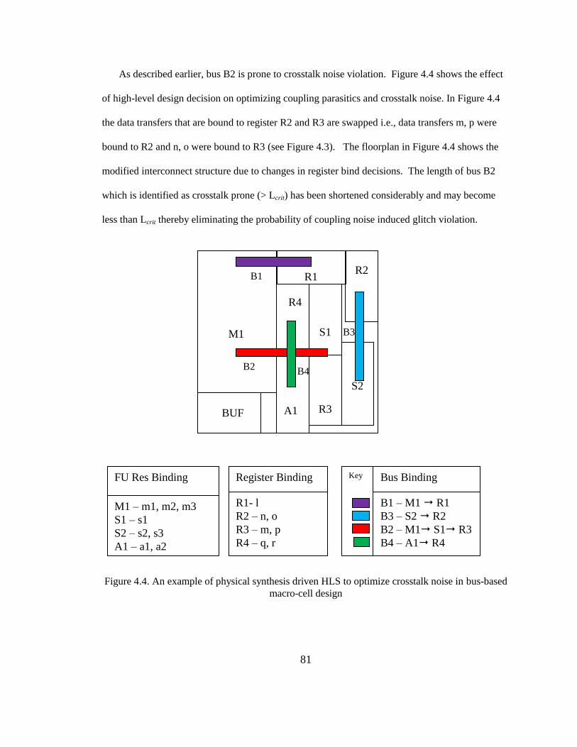
81
As described earlier, bus B2 is prone to crosstalk noise violation. Figure 4.4 shows the effect
of high-level design decision on optimizing coupling parasitics and crosstalk noise. In Figure 4.4
the data transfers that are bound to register R2 and R3 are swapped i.e., data transfers m, p were
bound to R2 and n, o were bound to R3 (see Figure 4.3). The floorplan in Figure 4.4 shows the
modified interconnect structure due to changes in register bind decisions. The length of bus B2
which is identified as crosstalk prone (> Lcrit) has been shortened considerably and may become
less than Lcrit thereby eliminating the probability of coupling noise induced glitch violation.
Figure 4.4. An example of physical synthesis driven HLS to optimize crosstalk noise in bus-based
macro-cell design
S2
M1
R1
R2
R4
A1
R3
BUF
S1
Key Bus Binding
B1 – M1 R1
B3 – S2 R2
B2 – M1 S1 R3
B4 – A1 R4
Register Binding
R1- l
R2 – n, o
R3 – m, p
R4 – q, r
FU Res Binding
M1 – m1, m2, m3
S1 – s1
S2 – s2, s3
A1 – a1, a2
B1
B2
B3
B4

82
This example clearly illustrates the fact that by integrating HLS and floorplan decisions it is
possible to optimize crosstalk noise violations at higher levels of design abstraction.
4.3 SA framework for floorplan driven HLS to minimize crosstalk violations
The main objective of the proposed floorplan driven HLS is to synthesize RTL netlist with
associated floorplan so that the resulting layout has minimum crosstalk violations. Simulated
annealing is extensively used to solve wide variety of intractable problems including HLS problem
[68, 69, 70, 71]. We justify applying SA framework to minimize crosstalk violations because: (a)
of its successful application to HLS domain; (b) simultaneous HLS-floorplanning problem can be
easily formulated; (c) the nature of SA is such that it refines the initial solution; i.e., a floorplan is
incrementally built taking into account the effect of HLS decision(s); and (d) for HLS problems, as
the DFG sizes are reasonable (few hundred nodes), the execution times are reasonable.
Given an input DFG the goal is to minimize number of crosstalk prone buses while optimizing
the latency and floorplan area as secondary goals. The cost function (C) is defined as:
normnormnorm XtalkbusWFPareaWlatWC *** 321 (4.1)
Where latnorm is the normalized latency (number of control steps), FParea is the normalized
floorplan area, and Xtalkbusnorm is the estimated number of crosstalk prone buses. W1, W2, and W3
are the relative weights. In this work, we set W1=0.25 W2=0.05 and W3=0.70 which are
determined empirically. Latency is normalized with respect to the ASAP schedule length. FParea
is normalized with respect to the area of the datapath for a parallel schedule. Xtalkbus is
normalized with respect to the total number of edge bits in the DFG.
Figure 4.5 shows the flow chart of the SA framework. The input is a DFG, resource
constraints, technology related data (Lcrit), and RTL library information. In the framework, the

83
# of moves per
temp < count
Technology
related data
(Lcrit)
Initial solution
(generated randomly)
DFG, User Specs, and
RTLIB dimensions
Perturb solution by
HLS/Floorplan moves
Update floorplan
Estimate bus length
based on topology
Calculate # of
crosstalk prone
buses
Evaluate cost function
Is solution better or
accept up-hill move
based on probability
Accept new solution
Yes
Decrement Temp (λ)
curr temp >
stop temp
No
Yes
Yes
No
No
Output
Crosstalk
Optimized RTL
netlist
and floorplan
Figure 4.5. Flow diagram for SA based floorplan driven HLS for crosstalk optimization

84
floorplan is represented as a sequence pair [95]. Two sets of moves are defined: (a) HLS moves;
and (b) Floorplan moves.
The following are the HLS-related moves:
Scheduling move alters the priority of operations in a list schedule. We employ list
scheduling algorithm.
Allocation move allocates or de-allocates FU resources such as adders, subtractors,
multipliers, etc.
Binding moves re-assigns module binding i.e., assigning an operation to a different
module instance or swap module bindings of compatible modules.
The following are the floorplanning related moves which alter the sequence pair representation to
explore floorplan solution space.
changing module orientation
swap module positions and
re-locate a module instance.
Given a bus with a set of bound data-transfers, the bus synthesis and floorplanning problem is
to determine the bus length as well as its location. This problem is solved by drawing a largest
rectangle such that the centers of all the modules involved are contained by the rectangle. We
illustrate this by an example. Consider five modules (A, B, C, D, and E) whose placements are as
shown in Figure 4.6. The encompassing rectangle is shown with a dotted line. The synthesized
bus is shown by a thick line and bisects the rectangle length wise. The length of the bus is equal to
the length of the encompassing rectangle. The framework could be easily extended to
accommodate bus-based floorplanning techniques proposed in [81, 83]. We reserve two layers for
bus routing and those two metal layers are not used for routing inside the macro-cells. In other
words, buses can run freely over any macro-cell blocks.

85
Figure 4.6. Illustration of bus synthesis and floorplanning step
4.4 Experimental results
The proposed SA based framework for crosstalk noise minimization has been implemented in
C and run on a SUN UltraSPARC 2. To validate the effectiveness of the proposed approach we
tested it on five data flow intensive DSP benchmarks. The synthesized RTL netlist generated by
the framework is then placed (adhering to the floorplan) and routed using Cadence-SOC
encounter. Cadence Fire & Ice parasitic extractor is used to extract parasitics from the routed
design. Finally, the Cadence Celtic crosstalk noise analysis is employed to determine number of
crosstalk violations.
4.4.1 Experimental setup and flow
Figure 4.7 shows the detailed experimental flow to determine the number of crosstalk
violations in a design. The commercial tools used are Cadence-SOC Encounter, Cadence Fire &
Ice parasitic extractor, Cadence Library generator (LibGen), and Cadence Celtic Crosstalk noise
analyzer. A digital macro-cell is a predefined module that implements a simple or complex digital
A
E
B
D
C
Largest
rectangle
containing
all module
centers
Synthesized
bus

86
Figure 4.7 Experimental flow
function that will be used frequently in a design. The complexity of a macro-cell block may vary
from few hundred gates to few thousand gates. The macro-cell based design technique offers the
designer the advantage of dividing the system into small independent blocks so as to reduce the
overall complexity of a design. The macro-cell blocks aids in design reuse i.e., implementing a
Proposed SA
framework
Cadence-SOC
encounter
Fire & Ice parasitic extraction
Routed design
(def file)
Macro-cell
layouts
LEF
Files
SPEF netlist with
coupling parasitics
Synthesized
RTL netlist
(verilog)
Floorplan
(placement
commands)
Inputs: DFG, user
constraints, and RT
Library dimensions
180nm technology
standard cell
library
# of noise nets
Technology
file (.tch)
LibGen
(Cadence cell
library)
Cadence Celtic
Crosstalk
Analyzer
Characterized noise
library for macro-
cells (UDN, cdB,
or ECHO)
Timing window
file and timing
constraints
87
digital function that will used frequently in a design such as multipliers, adders, filters etc. A soft
macro block doesnot have a fixed physical layout structure. It represents just a netlist of logic
gates. A hard macro block has fixed physical dimensions such as width and height. A hard macro
block is generated from a synthesized gate-level netlist implementing the required functionality
and the macro-cell layout is generated using standard cell place and route methodology. In our
proposed experimental flow, the synthesized gate-level netlist for each macro is generated by
AUDI HLS system. We employed OSU 180nm technology standard cell library [110], NCSU
design Kit, and Cadence-SOC Encounter to generate macro-cell layouts. Cadence LibGen was
used to create a binary view of all the macro-cell layouts. This step is necessary and it enables fast
extraction of parasitic information, since the macro-cells are used as building blocks for more
complex systems. For every macro-cell layout we run Cadence Fire & Ice Parasitic extractor and
Cadence Celtic crosstalk analysis and any crosstalk violations are fixed before the macro-cell is
used for building larger designs.
The inputs to the proposed SA based floorplan driven HLS framework are CDFG, user
constraints such as latency (in terms of control time steps), maximum number of resources to be
used, etc., and physical dimensions ie., height and width of hard macros representing the RTL
modules. The proposed framework generates a crosstalk noise optimized floorplan and
corresponding synthesized RTL netlist. Cadence-SOC Encounter is used to route the synthesized
netlist based on the generated crosstalk optimized floorplan information. Cadence Fire & Ice
Parasitic extractor is used to extract the coupling parasitics for the entire design as SPEF netlist
(Standard Parasitic Extraction Format).
Cadence Celtic crosstalk analysis tool requires SPEF netlist, characterized noise library model
(UDN model) for the macro-cells in a design, and routed design (DEF netlist). The user defined
noise model (or UDN) allows the user to specify the noise tolerance limit at each input pin of a

88
macro-cell. Celtic employs static noise analysis to propagate noise from inputs to outputs for each
macro-cell instance in a design. This analysis is based on calculating the worst-case noise
waveforms on each input and output nodes of the cell instance. Celtic assumes all possible worst-
case scenarios i.e., all the neighboring signal nets switch at the same time unless it is prohibited by
logic or timing constraints. If the worst-case noise waveform of a net driving an input pin of a
macro-cell is greater than the user defined noise threshold (UDN) then Celtic marks the
corresponding net as crosstalk prone net. In our experimental setup, we set the threshold to be
40% of VDD for combinatorial cells and 25% of VDD for sequential cells. In other words, if the
worst-case peak noise amplitude of a net that is driving a combinatorial block such as adder,
multiplier etc., is greater than 40% of VDD then the corresponding net is detected as a noise net.
Similarly, if the worst-case peak noise amplitude of a net driving a sequential block is greater than
30% of VDD then the corresponding net is considered to be a noise net. We have selected these
values based on the recommendations found in the Celtic User Manual [8].
4.4.2 Results and discussions
To validate the effectiveness of proposed approach we compared the number of noise nets
reported by Celtic for designs optimized through proposed framework versus multiplexer-based
designs generated through traditional HLS flow followed by floorplanning, placement, and
routing. The traditional HLS flow involves running scheduling, allocation, and binding
sequentially, followed by multiplexer-based interconnect, datapath, and control generation.
Cadence-SOC Encounter is then used to place and route the synthesized RTL netlist. We
conducted experiments under latency constrained environment. Latency is defined in terms of number
of control time steps.

89
Table 4.1 shows the benchmark details for five HLS benchmarks they are: 8-point DCT, 5th
order elliptic wave filter, FFT, mpeg for motion vector decoding, and auto regression filter (ARF)
[113]. DCT, FFT, and filters (EWF, ARF) benchmarks are selected because they are utilized in
majority of DSP applications. mpeg for motion vector decoding has highest level of parallelism
and moderate size. Column 2 lists the number of operations for each benchmark. Column 3-4
shows the number of data transfers and minimum latency. Column 5 lists the extent of parallelism
available in benchmarks.
Table 4.1 Benchmark details
BMs # of
nodes
# of
edges
Critical
path length
Parallelism
DCT
EWF
FFT
mpeg
ARF
43
34
36
32
28
35
47
28
29
30
7
14
6
6
8
6.14
2.43
6.00
5.33
3.5
Table 4.2 tabulates the results for the benchmarks synthesized by our proposed framework and
traditional sequential HLS flow. Column 2-3 reports the area for traditional and proposed flow.
Column 4-5 reports the average number of nets and macros in synthesized design. Column 6 lists
the number of buses in the design synthesized through proposed framework. Column 7-8 tabulates
the number of noise nets reported from Celtic crosstalk noise analysis. Column 8 reports the
percentage reduction in number of crosstalk violations. Column 9 reports the latency constraint
under which the benchmarks are synthesized by the proposed flow and traditional flow. Column
10 lists the area penalty for the proposed framework versus traditional HLS flow. Column 10
reports the SA execution time. For DCT, the floorplan driven approach provides the best result by
minimizing 96% of noise nets. For EWF, the crosstalk violations are reduced by 75% while for
FFT it is 96%. The proposed framework reduces crosstalk violation by 84% and 94% for mpeg
benchmark used for motion vector decoding and auto regression filter benchmark.

90
On average the proposed framework reduces the number of noise nets by 89%. These results
demonstrate convincingly that crosstalk noise can be optimized during early stages of design cycle.
The results also clearly demonstrate the superiority of the proposed approach. Figures 4.8-4.10
compares the coupling noise distribution of nets in the proposed framework and traditional
sequential flow. Cadence Celtic crosstalk analyzer was used to measure the crosstalk noise
amplitude of nets in a design. The crosstalk noise amplitude distribution is divided into four
regions. Region 1 shows the percentage of nets with peak noise amplitude greater than 0.8V (>
0.8V). Region 2 shows the percentage of nets with crosstalk noise amplitude between 0.6V and
0.8V. Region 3 shows nets between 0.4V and 0.6V and Region 4 shows the net distribution
between 0.2V and 0.4V. As stated earlier, peak noise amplitude greater than 0.54V (30% of Vdd)
on nets that drive the sequential block and greater than 0.72V (40% of Vdd) on nets that drive the
combinatorial block are considered as noise nets.
In Figure 4.8-A, 4.9-B, and 4.10, for DCT, mpeg, and ARF benchmarks the percentage of
nets in Region 2 (0.6V-0.8V) for proposed framework is less compared to traditional flow. While,
for FFT and EWF benchmarks the traditional flow results in lesser number of nets in Region 2
(0.6V-0.8V) compared to proposed work. Even though the proposed framework results in higher
percentage of nets in Region 2 the number of noise nets for proposed SA framework is very low
(refer Table 4.2) compared to sequential HLS flow. In other words, a majority of nets falling in
Region 2 (0.6v-0.8V) are nets driving combinatorial blocks and the noise amplitude in those nets
and is less than 0.72V (40% of Vdd). Since, the proposed SA driven framework simultaneously
explores both floorplan and HLS decisions it could explore for solutions for which the buses
driving the sequential block are of smaller length compared to buses driving combinatorial blocks.

91
Table 4.2. Crosstalk noise violations in proposed framework versus designs synthesized through traditional HLS flow
BMs Area (mm2) # of
nets
# of
Buses
# of
Macros
# of noise
nets
Savings
(%)
Latency
(csteps)
Area
Penalty
(%)
SA exec.
Time
(min) Seq SA Seq SA
DCT 14.55 14.55 3909 36 18 54 2 96.3 14 0 17
EWF 10.15 10.15 2632 25 18 56 14 75 16 0 15
FFT 34.81 41.76 8648 30 23 69 3 95.6 9 16.6 14
mpeg 10.91 12.96 4154 34 28 19 3 84.2 9 18.33 14
ARF 10.08 11.33 4219 32 26 18 1 94.4 10 12.35 13
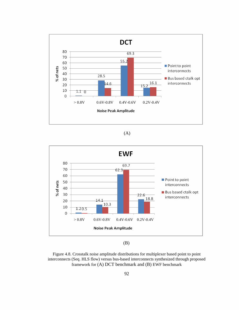
92
Figure 4.8. Crosstalk noise amplitude distributions for multiplexer based point to point
interconnects (Seq. HLS flow) versus bus-based interconnects synthesized through proposed
framework for (A) DCT benchmark and (B) EWF benchmark
(A)
(B)
> 0.8V 0.6V-0.8V 0.4V-0.6V 0.2V-0.4V
> 0.8V 0.6V-0.8V 0.4V-0.6V 0.2V-0.4V

93
Figure 4.9. Crosstalk noise amplitude distributions for multiplexer based point to point
interconnects (Seq. HLS flow) versus bus-based interconnects synthesized through proposed
framework for (A) FFT benchmark and (B) mpeg benchmark
(A)
(B)
> 0.8V 0.6V-0.8V 0.4V-0.6V 0.2V-0.4V
> 0.8V 0.6V-0.8V 0.4V-0.6V 0.2V-0.4V

94
Figure 4.10. Crosstalk noise amplitude distributions for multiplexer based point to point
interconnects (Seq. HLS flow) versus bus-based interconnects synthesized through proposed
framework for ARF benchmark
Figures 4.11-4.15 shows the crosstalk optimized bus-based floorplan for DCT, EWF, FFT,
mpeg –motion vector decoding function, and ARF benchmarks. The long and narrow vertical and
horizontal blocks are bus macros. The bus macros are a set of wires running in parallel connecting
the communicating modules. We have reserved two metal layers for bus routing; metal4 serves as
a vertical interconnect and metal5 as a horizontal interconnect. In other words, the routing inside
the macro-cells utilizes only three metal layers. This allows the buses to run freely over the macro-
cells constituting execution and storage units.
> 0.8V 0.6V-0.8V 0.4V-0.6V 0.2V-0.4V

95
4.5 Summary
In the proposed framework work, we demonstrate the feasibility of optimizing coupling
parasitics during high-level synthesis. The proposed approach simultaneously explores both HLS
and floorplan subspaces to synthesize bus-based designs with minimum crosstalk violations.
Coupling capacitance estimation is made possible by integrating an RTL floorplanner with HLS
engine. Experimental results from commercial tools show the proposed approach generates better
crosstalk immune designs than traditional ASIC design flow.

96
Figure 4.11. Crosstalk optimized bus-based floorplan generated by proposed floorplan driven HLS
for DCT benchmark

97
Figure 4.12. Crosstalk optimized bus-based floorplan generated by proposed floorplan driven HLS
for EWF benchmark

98
Figure 4.13. Crosstalk optimized bus-based floorplan generated by proposed floorplan driven HLS
for FFT benchmark

99
Figure 4.14. Crosstalk optimized bus-based floorplan generated by proposed floorplan driven HLS
for mpeg benchmark

100
Figure 4.15. Crosstalk optimized bus-based floorplan generated by proposed floorplan driven HLS
for ARF benchmark

101
CHAPTER 5
ON-CHIP DYNAMIC WORST-CASE CROSSTALK PATTERN DETECTION AND
ELIMINATION FOR BUS-BASED DESIGNS
In this chapter, we present an on-chip crosstalk pattern detection and elimination circuit to
eliminate worst-case coupling transition pattern. In high speed nanometer designs the coupling
capacitances between the adjacent wires on same metal layer dominate the total wire capacitance
causing large delay variations and also compromise the noise immunity of the signal. The effect of
coupling capacitances on signal propagation delay is further influenced by signal transition
patterns on the victim and neighboring aggressor nets. As described in chapter two, a worst-case
coupling transition pattern in a two aggressor model occurs when the signals on both the aggressor
nets switches in a direction opposite to that of a victim net. In a two aggressor model such a worst-
case coupling transition pattern is generally referred to as 4Cc crosstalk pattern.
The 4Cc crosstalk pattern causes the maximum increase in the propagation delay of a signal
and may lead to setup time violation if the signal drives an input of a flip-flop or latch. In a bus-
based interconnect architecture this effect is more acute because the bus cycle time has to be
designed based on the propagation delay of worst-case crosstalk pattern. Design based on such
pessimistic estimate is not desirable because not all signal transitions might result in worst-case
propagation delay and thus will adversely impact the performance of the system. Therefore, we
propose an on-chip worst-case crosstalk pattern detection and elimination circuit which
dynamically detects the worst-case crosstalk pattern (or 4 .Cc crosstalk patterns) and eliminates it
by postponing the transmission of data pattern for one clock cycle and instead transmit logic zero

102
value on the bus during the current cycle. The proposed technique incurs a penalty of one clock
cycle per detection and elimination of worst-case pattern. The area overhead of the proposed
technique is also minimal when compared to other crosstalk optimization techniques such as
shielding, double spacing, and encoding techniques.
The rest of the chapter is organized as follows: Section 5.1 presents a motivational example.
Section 5.2 describes in detail the proposed dynamic crosstalk pattern detection and elimination
scheme. Section 5.3 reports the experimental results. Section 5.4 draws conclusions.
5.1 An illustrative example
Figure 5.1 shows a scheduled DFG, a corresponding functional resource and bus binding
solution, and a sample execution trace. As it can be seen in Figure 5.1 the DFG has 4 add and 2
multiply operations. All data transfers are 4 bits wide (i.e., bus width is 4 bits). Data transfer e is
bound to Bus B1. Bus B2 is shared by data transfers f, g, and out and B3 is shared by n and h. The
buses are shared based on the lifetime of the data transfers. In other words, two data transfers can
share a bus if and only if their lifetimes do not overlap. For the sample execution trace shown in
Figure 5.1 the bus B2 will transmit f = “0101” at T=2 and g = “1010” at T=3 on bus B2. This will
lead to worst-case crosstalk pattern on three LSBs of bus B2 i.e., in bus B2 bit b1 is flanked by bits
b0 and b2 on either side. Due to temporal correlation between f and g, the bit b1 transitions from 1
(at T=2) to 0 (T=3) and the neighbors b0 and b2 transitions from 0 to 1. This causes a worst-case
coupled signal transitions between b2, b1, and b0 and will increase the propagation delay on bus B2
due to Miller coupling effect. The most straight forward approach is to perform static timing
analysis to calculate the worst-case delay for a bus. Based on this conservative estimate, the bus
cycle time is fixed to avoid crosstalk noise induced delay failures.

103
Figure 5.1. (A) Scheduled DFG, (B) A sample execution trace, and (C) A possible bus-based
datapath
+
b
e
a
a1
+
c d
f *
g
m2
T=1
T=2
T=3
T=0
a2
*
h
k
+
a3
j
n
m
1
ADD1
B1 B2 B3
MULT1
a
c
b
d
e f
e f
g
j k
ADD2
n n
h
d
Partial Execution Trace:
a = 0001, b = 0001, c = 0011, d = 0010
e = a + b = 0010
f = c + d = 0101
g = e * f = 1010
Bus Binding:
B1: {e}
B2: {f, g, out}
B3: {n, h}
FU Res Binding:
MULT-1: {m1, m2}
ADD-1: {a1, a2,
a3, a4}
+ T=4
out
a4
(A) (B)
(C)

104
Timestep Original design With proposed scheme
Operation Data
transfer
Data Operatio
n
Data
transfer
Data
1 - - - - - -
2 a2 f 0101 a2 f 1010
3 m2 g 1010 - all zero 0000
4 a4 out 1100 m2 g 1010
5 a4 out 1100
Figure 5.2. Execution trace on bus B2 for original design versus proposed scheme
As an alternative to this pessimistic scheme, we propose a more efficient dynamic crosstalk
detection and elimination scheme to automatically detect and eliminate worst-case crosstalk noise
induced delay with minimum speed penalty. In the proposed approach the worst-case crosstalk
pattern is eliminated by manipulating the temporal correlation between adjacent data transfers
bound to a bus. For example, considering the same execution trace as discussed above at T=2 the
bus B2 will transmit f = “0101”. At T=3, the data transfer g = “1010” will be forbidden for
transmission on bus B2. Instead an all zero data pattern (“0000”) will be transmitted on B2 at T=3
and all the operations at T=4 (a4, adder operation) and later will be postponed by one clock cycle.
At T=4, the data transfer g = “1010” will be transmitted on bus B2 thereby eliminating worst-case
crosstalk induced delay due to data patterns of f and g.
Figure 5.2 shows the execution trace on bus B2 for the design with and without proposed
dynamic detection and elimination circuit. For the example shown in Figure 5.2 the proposed
approach incurs a penalty of one clock cycle when a worst-case crosstalk pattern is detected. The
output of operation m2 (g) which causes a worst-case coupling transition with output of a2 (f) is
delayed for one clock cycle and the design takes five clock cycles to complete its execution. The
advantage of proposed approach is it can result in higher clock frequency, because the worst-case
crosstalk induced propagation delay never happens thereby enhancing the performance of designs.

105
5.2 Proposed on-chip worst-case crosstalk pattern detection and elimination technique
The proposed technique operates in two stages: (a) Stage 1- crosstalk detection; and (b) Stage
2 - worst-case coupling transition pattern elimination. In the first stage the crosstalk detection unit
checks for the occurrence of worst-case crosstalk pattern. This is accomplished by comparing the
data transmitted on a bus in the previous cycle with the data that will be transmitted in the current
clock cycle. In other words, every word is checked for violation before it is transmitted on the bus.
Figure 5.3 shows a gate-level circuit implementing the proposed crosstalk detection technique for
one bus line (b1). The bit sequence {p0, p1, p2} represents the data transmitted in the previous
clock cycle and {c0, c1, c2} denotes the data to be transmitted in the current cycle. Figure 5.3
shows a scenario where a signal in bit b1 is transitioning from logic „1‟ to logic „0‟ (i.e.,
p1=1c1=0), while, its neighboring bits b0 and b2 are switching in opposite direction (p0=0c0=1,
p2=0c2=1) and vice versa. Because of Miller coupling effect such opposite transitions will lead
to worst-case propagation delay on b1.
Technically speaking, each and every bus line acts as an aggressor or victim net. Therefore, a
4-bit bus requires an array of four such gate-level circuits to detect the occurrence of “010” and
“101” pattern in previous and current data transmitted on a bus. Similarly, a second array of four
gate-level circuits is required to detect “101” and “010” pattern in previous and current data.
Figure 5.4 shows an example of crosstalk detection unit for a 4-bit bus. In Figure 5.4, a 4-input
OR-gate ensures that each and every wire in a bus is free from worst-case coupling transition. In a
bus-based interconnect architecture as the buses are synchronized with respect to a clock, it is
required that all the individual lines comprising a bus must be crosstalk free. The output of 4-
input OR- gate will be 1 if there is a violation in at least one bus line. Therefore, when there is a
violation in the current data it will be postponed for one clock cycle. Instead bus will be reset

106
Figure 5.3. Gate-level circuits for worst-case crosstalk pattern detection
implying logic „0‟ will be transmitted on the bus during current cycle. In the following cycle, the
original data will be transmitted on the bus i.e., after a delay of one clock cycle.
5.2.1 AUDI design framework
Given a CDFG, we first synthesize the design through AUDI behavioral synthesis system
[109]. The output of AUDI is a RT-Level datapath and a behavioral controller. A behavioral
controller implements a state machine and generates required control signals for the datapath units.
It also responds to the status or feedback signals from the datapath. The controller operates during
p0
p1
p2
c0
c1
c2
Data
transmitted
in previous
clock cycle
Data to be
transmitted
in current
clock cycle
c0
c1
c2
p0
p1
p2
Data
transmitted
in previous
clock cycle
Data to be
transmitted
in current
clock cycle
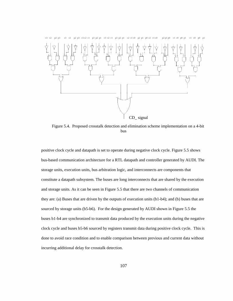
107
Figure 5.4. Proposed crosstalk detection and elimination scheme implementation on a 4-bit
bus
positive clock cycle and datapath is set to operate during negative clock cycle. Figure 5.5 shows
bus-based communication architecture for a RTL datapath and controller generated by AUDI. The
storage units, execution units, bus arbitration logic, and interconnects are components that
constitute a datapath subsystem. The buses are long interconnects that are shared by the execution
and storage units. As it can be seen in Figure 5.5 that there are two channels of communication
they are: (a) Buses that are driven by the outputs of execution units (b1-b4); and (b) buses that are
sourced by storage units (b5-b6). For the design generated by AUDI shown in Figure 5.5 the
buses b1-b4 are synchronized to transmit data produced by the execution units during the negative
clock cycle and buses b5-b6 sourced by registers transmit data during positive clock cycle. This is
done to avoid race condition and to enable comparison between previous and current data without
incurring additional delay for crosstalk detection.
c3 c2 p2 p3 c3 c2 p2 p3 c3 c2 c1 p3 p2 p1 c3 c2 c1 p3 p2 p1 c2 c1 c0 p2 p1 p0 c2 c1 c0 p2 p1 p0 c1 c0 p0 p1 c1 c0 p0 p1
CD_ signal

108
Figure 5.5 Typical bus-based interconnect structure generated by AUDI
5.2.2 Modified RTL design model implementing proposed technique
Figure 5.6 shows the modified RTL datapath and controller design implementing the proposed
approach. Each execution and storage unit is fitted with individual crosstalk detection units (CD)
and buffers. The buffer holds the data transmitted on a bus during the previous cycle. Figure 5.6
also shows multiple instances of crosstalk detection units and buffers within each execution and
storage modules. This is due to the fact the execution and storage modules are sourcing more than
one bus and the total number of instances per module depends on the number of buses driven by
each module. For example in Figure 5.6, the output of multiplier is driving two buses b1 and b2.
Therefore, there are two instances of buffers and crosstalk detection units (Figure 5.4 shows the
crosstalk detection unit for a 4-bit bus). The multiplier and adder module in Figure 5.6 share the
b3
b6 b5 b4
b2 b1
C
O
N
T
R
O
L
L
E
R
EXECUTION UNITS
MULT MULT ADD SUB
REG REG REG REG
STORAGE UNITS
ctrl_signals

109
Figure 5.6. Modified architecture implementing proposed crosstalk detection and elimination
technique
bus b1 implying at any time step only one of the module will be allowed to transmit the data on
bus b1. However, one could argue that instead of having an instance of crosstalk detection unit in
each execution unit driving the bus it would be better to have just one global crosstalk detection
unit for each bus and thereby incurring less area penalty. On the other hand, an equally effective
counter argument is by having a local instance of crosstalk detection unit and buffer for each bus
will ensure shorter interconnects between the execution unit and the crosstalk detection unit. The
b1
C
O
N
T
R
O
L
L
E
R
b3
b6 b5 b4
b2
REG
Buf
1
Buf
1
CD CD
REG
Buf
1
Buf
1
CD CD
STORAGE
UNITS
MUL
Buf
1
Buf
1
CD CD
ADD
CD CD
Buf
1
Buf
1
EXECUTION
UNITS
CD signal
ctrl_signals

110
shorter interconnects are unlikely to suffer crosstalk noise effects. This is similar to cache and main
memory trade-off to optimize the performance of a system. This is just an implementation issue
and designers are free to choose any implementation style to suit their requirements.
Figure 5.7-A to C shows the implementation details of proposed scheme on a bus-based
macro-cell design synthesized through HLS engine shown in Figure 5.6. For the sake of clarity
Figure 5.7-A shows only the crosstalk detection and elimination circuit for bus b1. Bus b1 is
shared by multiplier and adder blocks. A crosstalk detection unit (CD) (refer Figure 5.3) compares
the output of an execution unit (i.e., current data from multiplier or adder) with the data
transmitted on the bus in the previous clock cycle stored in a buffer. Figure 5.7-B shows the buffer
synchronized with respect to a clock. Since the buses driven by execution units are synchronized to
transmit data only during negative cycle, the buffer also remains enabled during negative clock
cycle. Figure 5.8 shows the circuit implementation of proposed crosstalk elimination scheme. The
clk signal to the crosstalk elimination (CE) block ensures the data is transmitted only during the
negative clock cycle. The wr_mult/wr_add signal from the controller ensures that only one of the
blocks is sourcing the bus at any time step. For the example circuit shown in Figure 5.8, the
output of the MULT block (i.e., current data) will be transmitted on bus b1 only if wr_mult is 1
and CD_signal is 0. In case of detection of worst-case crosstalk pattern, CD_signal will be 1 and if
wr_mult is also 1 then the transmission of actual data from the multiplier will be postponed for one
clock cycle, instead the crosstalk elimination unit will transmit a logic „0‟ data value on the bus.
As already explained in Section 2 that the transmission of logic „0‟ value eliminates the occurrence
3Cc and 4Cc crosstalk patterns on buses.
Figure 5.9-A shows the finite state machine implementation of behavioral controller for
scheduled, allocated, and bound DFG in Figure 5.1 and Figure 5.9-B shows the block diagram for
the AUDI generated RTL model. The controller is synthesized such that each time step is mapped

111
Figure 5.7. Block diagram for crosstalk detection and crosstalk elimination circuit in bus-based
macro-cell designs
wr_mult
BUF
clk clk
clk clk
wr_add
previous
data current
data
CD_signal
(A)
Bus
(B1)
CD
MULT ADD
CD BUF
CE CE
clk‟ clk
previous
data
From
bus
Buffer
(B)

112
Figure 5.8. Crosstalk elimination circuit
to one clock cycle. The duration of clock cycle is determined by the worst-case propagation delay
of a bus. By eliminating the worst-case propagation delay which occurs due to worst-case coupling
transitions, the designs can employ faster clocks and thereby enhance the performance of the
design. The first state is an idle state and at the assertion of start signal the primary inputs are
latched on to the registers. The state machine implemented is a mealy model i.e., the outputs are
function of both inputs and present state. The inputs to the controller are feedback signals (or
flags) from the datapath units and the crosstalk detect signal (CD_signal) from crosstalk detect
unit. The controller generates signals to control the operations of datapath units. Figure 5.9-A
shows the state transitions and the corresponding outputs (i.e. the control signals) generated at
each control step (or time step). The state transitions occur only in the absence of worst-case
crosstalk violation (i.e., CD_signal = „0‟). If there is a crosstalk violation (CD_signal = „1‟) then
the state machine loops in the same state and the output of the controller (i.e., control signals) will
remain the same. The controller maintains the same set of control signals until the actual data is
transmitted on the bus and latched on to the register thereby ensuring functional correctness of a
design.
CD_signal
GND
current data
from MULT
CD_signal
wr_mult
clk
wr_mult
Crosstalk Elimination
Circuit (CE) Block
Bus
(B1)

113
Figure 5.9. AUDI controller (A) Mealy model based state diagram for DFG shown in Figure 5.1
(B) Block diagram depicting the RTL model synthesized by AUDI with proposed crosstalk
detection scheme
5.3 Experimental results
We first synthesize the behavioral specification of a design using AUDI behavioral synthesis
tool. The synthesized VHDL netlist is modified to incorporate the proposed technique and is
simulated using Cadence NCSim simulator. Experiments were conducted to verify the functional
correctness of the modified RTL design with crosstalk detection unit. Figure 5.10 shows a
snapshot of simulation results for IIR filter design. The first instance of worst-case crosstalk
start
0 /ctr_s0
1 /ctr_s0
1 /ctr_s1
1/ctr_s2
1/ctr_s3
1/ctr_s4
0/ctr_s1
0/ctr_s2
0/ctr_s3
0/ctr_s4
finish
Datapath
Primary
Inputs
Primary
Outputs
Flags
Control
Signals
CD_signal
Combinational logic
Memory
Controller
State
outputs State
Inputs
CD_signal control signals
start finish
clock
clock
reset
reset
(A) (B)

114
Figure 5.10. Simulation results for IIR filter design implementing the on-chip crosstalk elimination
technique
pattern occurs on Bus1 (i.e. Bus1_out). As shown in Figure 5.10 the data transmitted on the bus
when the state machine is in state S4 is “0010” and the data to be transmitted when the current
state is S5 is “0101”. However, this will lead to a worst-case crosstalk pattern on Bus1. Therefore,
instead of transmitting current data “0101” on Bus1 the bus is reset to zero thereby eliminating
Table 5.1. Characteristics of different data transmission methods [18]
Bus
Transmission
methods
Cg
(fF/mm)
Cc
(fF/mm)
Number
of wires
Normalized
cycle time
ORI 36.3 115.1 32 3.28
CPC 36.3 115.1 53 2.76
DBS 53.1 60.4 32 1.95
SHD 36.3 115.1 63 1.76
DYN 36.3 115.1 33 1.00
CD flag = „1‟
Previous
data Current
data
Worst-case
crosstalk
elimination
pattern

115
worst-case crosstalk pattern induced delay on the bus. Then in the next control step (i.e. at S6) the
data “0101” which should have been transmitted during S5 gets transmitted after a delay of one
clock cycle. Similarly, another instance of crosstalk violation on Bus0 (i.e. Bus0_out) is
eliminated by the proposed technique. The proposed approach can also be implemented easily
across various bus-based designs such as on-chip memory buses, on-chip buses of a
microprocessor, bus-based macro-cell designs, etc.
Table 5.1 is reproduced from crosstalk aware variable cycle transmission work in [18]. The
authors in [18] have compared the effectiveness of their proposed technique (DYN) versus other
transmission techniques such as Original (ORI), Crosstalk prevention codes (CPC), Double
spacing (DBS), and Shielding (SHD). In the original transmission method (ORI) the bus cycle
time is fixed based on the pessimistic estimate of worst-case propagation delay i.e. Tclk = (Cg +
4Cc)Rtotal. CPC transmission technique implements encoding scheme to eliminate worst-case
crosstalk pattern (4Cc). Therefore, the bus cycle time is Tclk = (Cg + 3Cc)Rtotal. DBS implies double
spacing method where the spacing between adjacent bus lines is set to two times the minimum
wire separation for a given target technology. For this experiment, the authors in [18] considered
0.25μm technology and the wire separation are set to 0.64μm. Since coupling capacitance is
inversely proportional to extent of wire separation increasing the separation will result in reduced
Cc as shown in Table 5.1 (refer row 3, column 2). SHD refers to shielding where Vdd or Ground
lines are inserted between every pair of wires. By having shield wires on either side prevents
simultaneous switching in opposite direction on adjacent wires thereby eliminating 4Cc and 3Cc
crosstalk patterns. Therefore, the bus cycle time is set based on propagation delay for 2Cc
crosstalk pattern i.e. Tclk = (Cg + 2Cc)Rtotal.
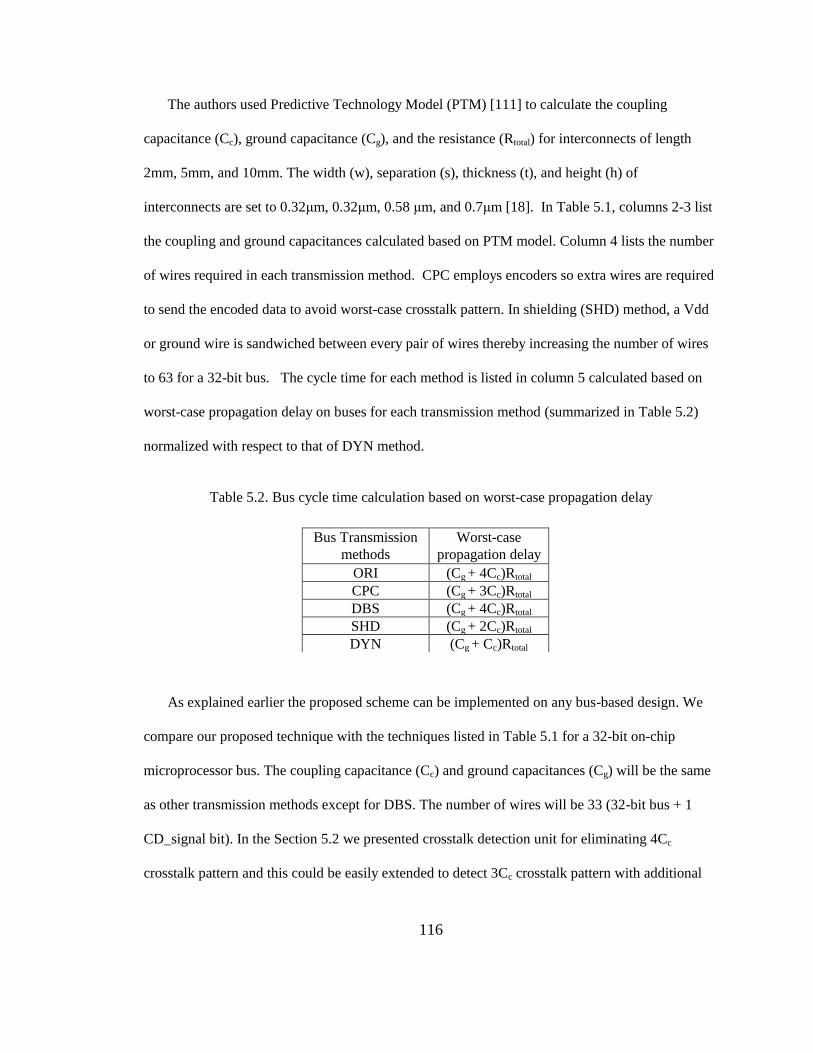
116
The authors used Predictive Technology Model (PTM) [111] to calculate the coupling
capacitance (Cc), ground capacitance (Cg), and the resistance (Rtotal) for interconnects of length
2mm, 5mm, and 10mm. The width (w), separation (s), thickness (t), and height (h) of
interconnects are set to 0.32μm, 0.32μm, 0.58 μm, and 0.7μm [18]. In Table 5.1, columns 2-3 list
the coupling and ground capacitances calculated based on PTM model. Column 4 lists the number
of wires required in each transmission method. CPC employs encoders so extra wires are required
to send the encoded data to avoid worst-case crosstalk pattern. In shielding (SHD) method, a Vdd
or ground wire is sandwiched between every pair of wires thereby increasing the number of wires
to 63 for a 32-bit bus. The cycle time for each method is listed in column 5 calculated based on
worst-case propagation delay on buses for each transmission method (summarized in Table 5.2)
normalized with respect to that of DYN method.
Table 5.2. Bus cycle time calculation based on worst-case propagation delay
As explained earlier the proposed scheme can be implemented on any bus-based design. We
compare our proposed technique with the techniques listed in Table 5.1 for a 32-bit on-chip
microprocessor bus. The coupling capacitance (Cc) and ground capacitances (Cg) will be the same
as other transmission methods except for DBS. The number of wires will be 33 (32-bit bus + 1
CD_signal bit). In the Section 5.2 we presented crosstalk detection unit for eliminating 4Cc
crosstalk pattern and this could be easily extended to detect 3Cc crosstalk pattern with additional
Bus Transmission
methods
Worst-case
propagation delay
ORI (Cg + 4Cc)Rtotal
CPC (Cg + 3Cc)Rtotal
DBS (Cg + 4Cc)Rtotal
SHD (Cg + 2Cc)Rtotal
DYN (Cg + Cc)Rtotal

117
Figure 5.11. Distribution of coupling signal transition pattern for SPEC2000 benchmark suite [18]
circuitry similar to the one shown in Figure 5.3. The bus cycle time is set to the propagation delay
for 2Cc crosstalk pattern and the normalized cycle time is 1.76 with respect to DYN transmission
method.
The authors in [18] have used Simplescalar 3.0 tool-set and SPEC2000 CINT [112]
benchmark suite to simulate the performance of the data bus connecting the processor datapath and
L1 D-cache. Figure 5.11 shows the data distribution based on the coupling signal transition
pattern for SPEC2000 benchmark suite reproduced from [18]. Figure 5.12 shows the performance
of transmission methods in terms of number of bus cycles used for transmission normalized with
respect to bus cycle time shown in Table 5.1.

118
Figure 5.12. Performance comparison of proposed approach versus other transmission methods
implemented in [18]
In Figure 5.12 we compare the performance of the proposed approach versus all the other
transmission methods implemented in [18]. It can be seen that SHD is the best and DBS results
comes second for all the benchmarks except for mcf. SHD and DBS yield good performance at
the expense of large area overhead. In case of SHD, the total bus area will be two times greater
than that of ORI, DYN, and proposed transmission methods. In case of DBS, the increased wire
separation between each pair of adjacent wires will lead to a large area penalty. The proposed
approach and DYN transmission method are really competitive across all benchmarks except for
mcf benchmark. On average, the proposed approach incurs a penalty of 18 more clock cycles than
DYN transmission method. From Figure 5.11 we can see that for mcf benchmark 65% of
transitions belong to Cc signal transition patterns and having a faster clock will clearly enhance the

119
performance. Which is the case with DYN method whose normalized clock time is 1.0 compared
to 1.76 for the proposed approach. In other words, the total cycle time to transmit 65% of Cc
pattern is 65.0 for DYN and 65 * 1.76 = 114.4 for proposed approach. However, the proposed
approach incurs less area penalty compared to DYN, because DYN method requires additional
circuitry to detect 2Cc signal transition pattern. Another interesting observation is that the
proposed methodology is efficient in handling 4Cc and 2Cc crosstalk patterns. While, DYN
method will work well for 3Cc and Cc crosstalk patterns. Table 5.3 shows the normalized cycle
time for transmitting different signal patterns using DYN and the proposed method. For example,
the proposed technique takes two clock cycles to transmit 4Cc transition pattern i.e., Tclk(4Cc) =
1.76 * 2 = 3.52 normalized cycle time. While DYN takes four clock cycles or Tclk(4Cc) = 1 * 4 =
4.00 normalized cycle time.
Table 5.3. Normalized bus cycle time to transmit different coupling signal transition pattern in
DYN and proposed transmission method
Bus Transmission
methods
Norm. bus transmission time for
different transition patterns
4.Cc 3.Cc 2.Cc Cc
DYN 4.0 3.0 2.0 1.0
Proposed 3.52 3.52 1.76 1.76
Figure 5.13 shows the performance comparison in terms of number of bus cycles for DYN and
proposed approach for negating the impact of 4.Cc and 3.Cc crosstalk patterns on propagation
delay. The bus cycle time will be set to propagation delay for 2.Cc crosstalk pattern. From Figure
5.13 it is clear that the proposed approach is better than the DYN transmission method for all the
benchmarks in SPEC2000 benchmark suite. On average, DYN approach takes 152 clock cycles
compared to 138 clock cycles for the proposed approach. This is due to the fact the proposed
approach takes two clock cycles to transmit 4Cc or 3Cc signal transition patterns. On the other

120
Figure 5.13. Performance comparisons between DYN and proposed approach to negate 4Cc and
3Cc signal transition pattern induced delay
hand, the DYN approach will take 4 and 3 clock cycles respectively to transmit 4Cc and 3Cc signal
transition patterns. Hence, we could conclude that for benchmarks with significant percentage of
4Cc signal transition patterns the proposed approach ensures better performance than DYN
method with same area penalty.
We also conducted experimental analysis on four HLS benchmarks synthesized by AUDI HLS
framework. Table 5.4 shows the characteristics of different techniques for synthesized designs.
Synthesized DCT netlist has 32 buses each 32 bit wide (32*32=1024). EWF, FFT, and IIR
benchmarks have 15, 8, and 3 buses respectively. Columns 2-5 report the number of wires
required to implement the buses for different benchmarks. Column 6 reports the normalized bus
cycle time calculated based on equations in Table 5.2 and RC values in Table 5.1. Column 7

121
reports the bus area overhead. SHD results in highest bus area overhead followed by ENC and
DBS compared to ORI. On the other hand, the proposed approach incurs a small penalty of 3%
compared to ORI.
Table 5.4. Characteristics of designs implementing different crosstalk delay optimization
techniques
No. of wires Norm.
cycle time
Norm.
bus area DCT EWF FFT IIR
ORI 1024 480 576 96 1.86 1.00
CPC 1696 795 954 159 1.43 1.66
DBS 1024 480 576 96 1.10 1.50
SHD 2048 960 1152 192 1.00 2.00
Proposed 1056 495 594 99 1.00 1.03
Figure 5.14 shows the data distribution for four HLS benchmarks obtained by profiling the
designs for three different signal environments (S1, S2, and S3). The data patterns are classified
based on the Miller coupling factor (MCF). The input signals for the experiments are generated
based on the ARMA equation [30, 87]:
x(n) = µx γ(n) + σx + ρx x(n − 1) (5.1)
where μx, σx, and ρx are the word-level statistical parameters, namely, mean, standard
deviation, and temporal correlation coefficient. The ARMA equation in (1) is a first order ARMA
model as the value of signal x(n) is dependent only on its prior value. This temporal dependence is
modeled as temporal correlation coefficient (ρx). The noise term γ(n) is discrete and has a standard
normal distribution. By varying these parameters, different data streams can be generated.
Temporal dependence of the signal x(n) on its previous value can be varied by temporal
correlation coefficient (ρx).

122
Figure 5.14. Data pattern distribution based on MCF for HLS benchmarks
Figure 5.15 shows the performance of different techniques normalized in terms of number of
clock cycles required to transmit the data patterns shown in Figure 5.14. It can be seen that
designs with SHD technique results in best performance. On average it improves performance by
60% compared to Orig (or ORI) design. This is due to the fact that the inserted shield wires
eliminate worst-case propagation delay due to 4Cc and 3Cc crosstalk patterns. Therefore, it takes
only one clock cycle to transmit any type of data pattern. A major drawback of SHD is it incurs
~100% area overhead and is impractical for very large designs. DBS comes second best with
average performance improvement of 53% and also incurs a significant area penalty (~50%)
compared to ORI (or Orig) design. On the other hand, the proposed technique provides 23%
performance improvement over ORI with a bus area penalty of just 3%. While ENC is marginally

123
Figure 5.15. Performance comparison of proposed approach versus other crosstalk delay reduction
techniques
better for benchmarks with high percentage of 4Cc crosstalk patterns compared to proposed
technique. On average, ENC enhances performance by 30% with an area penalty of 66%. In
addition, ENC requires CODECs and our technique requires CD and CE units to eliminate worst-
case crosstalk patterns. Table 5.5 shows the logic overhead for the proposed technique in terms of
percentage of additional gates required to implement CD and CE blocks compared to ORI design.
Even though the proposed technique incurs an additional logic overhead compared to techniques
with no logic overhead such as SHD and DBS, this overhead is very small compared to bus area
overhead of SHD and DBS schemes. In other words, for interconnects of any length the logic
overhead of proposed technique will remain constant. On the other hand, for SHD and DBS

124
techniques due to additional wires and spacing requirements the bus area will increase with
increase in interconnect length.
Table 5.5. Logic overhead
Benchamrks Logic Overhead
DCT 38%
EWF 20%
FFT 25.6%
IIR 24%
The proposed on-chip crosstalk detection and elimination circuit will improve performance
further for designs synthesized using our proposed SA based worst-case crosstalk pattern
minimization framework described in Section 3.1. Figure 5.16 shows the percentage of worst-case
crosstalk pattern minimized for HLS benchmarks synthesized through our proposed SA based
framework. It reports the average worst-case savings presented in Table 3.5. We observed that
the proposed on-chip crosstalk technique incurs a speed penalty of one clock cycle per worst-case
crosstalk violation. By reducing the frequency of worst-case signal transitions the speed penalty
will decrease further thereby enhancing the overall performance of the design. Implementation of
proposed dynamic on-chip technique on such designs resulted in an average performance
improvement of 28% compared to ORI. The on-chip technique also enhances the robustness of
designs synthesized by SA framework, as the SA based framework optimizes designs based on a
given data environment. A general limitation of all profile driven optimization techniques is what
will happen if the real-time input traces have different characteristics such as mean, standard
deviation, and temporal correlation from that of input data profile. In such a scenario, the proposed
on-chip elimination technique provides an extra layer of security by ensuring crosstalk violations
are filtered out completely and thereby ensuring signal reliability. From the above discussion, we

125
Figure 5.16. Percentage of worst-case crosstalk pattern minimized for HLS benchmarks by
proposed SA based framework
can conclude that the proposed technique and proposed SA based framework works well in unison
enhancing the performance and robustness of designs.
5.4 Conclusions
We have presented an on-chip crosstalk detection and elimination circuit to dynamically
eliminate worst-case crosstalk patterns with minimum speed penalty. This is accomplished by
transmitting a worst-case crosstalk elimination pattern (logic „0‟) per worst-case crosstalk
detection. The technique can be easily incorporated in the HLS flow or could be added separately
as a macro block to a synthesized RTL or gate netlist. The proposed approach also requires less
chip area compared to shielding, double spacing, and encoding techniques.

126
CHAPTER 6
CONCLUSIONS AND FUTURE WORK
Crosstalk noise is a function of metrics such as coupling parasitics, driver strength, signal
timing characteristics, and coupled signal transition patterns. Experts have pointed out that one in
five chips fail due to crosstalk induced signal integrity issue. Due to the criticality of problem and
the tight schedule generally associated with a project to maintain the competitiveness in market it
is critical to optimize for crosstalk at all stages of design cycle. Therefore, we have proposed a
high-level synthesis framework to optimize for coupled signal transition pattern in bus-based
macro-cell designs. The partial neighborhood definition available in bus-based designs is explored
judiciously during high-level synthesis process to minimize number of crosstalk violations. In
addition, optimization at higher levels of design abstraction offers the advantage of fast design
space exploration which is exploited by the proposed Simulated Annealing based framework to
minimize worst-case transition pattern thereby eliminating worst-case noise delay on buses. We
have shown that a worst-case crosstalk pattern is dependent on data correlations which in turn
depend on resource sharing which in turn is dependent on high-level synthesis tasks. So, the
proposed framework simultaneously explores the HLS, re-ordering, and encoding subspaces to
minimize worst-case crosstalk patterns. Results have shown that the proposed high-level
framework benefits the low level crosstalk analysis and repair tools by eliminating false positive
violations thereby reducing the number of noise nets and the time required to repair and fix
crosstalk violations.

127
We have also proposed another high-level framework based on Simulated Annealing based
design space exploration for eliminating problematic noise nets by optimizing another critical
crosstalk metric, the coupling capacitance. Estimation of coupling capacitances requires physical
level details such as neighborhood information, length of overlap, and wire spacing details for
every net in the design. In bus-based macro-cell designs the neighborhood is predefined and wire
spacing between the bus lines are constant. So, to estimate overlap length we integrated a
floorplanner with the high-level synthesis engine. We have characterized the technology node to
determine the critical bus length, which is the minimum bus length above which the bus may
suffer crosstalk noise. The framework explored high-level and low level design decisions and
generated designs with minimum number of crosstalk prone nets. The optimized design was then
placed and routed using Cadence-SOC Encounter. Cadence Celtic tool was then employed to do
layout level crosstalk analysis. Experimental results from Cadence Celtic have validated the
effectiveness the proposed floorplan driven high-level synthesis framework.
Finally, we proposed a dynamic on-chip crosstalk detection and elimination technique to
eliminate worst-case crosstalk patterns with minimum performance penalty. The proposed
technique eliminated worst-case crosstalk pattern by delaying the transmission of actual data and
instead transmitting a logic zero data value per detection of worst-case event on buses. It was also
shown that the proposed technique complements the SA based framework and the results have
validated the claim.
The directions for future work to optimize crosstalk at higher levels of design abstraction are
listed here:
In the floorplan driven high-level synthesis framework we have presented a simple
procedure to determine the bus length and its location. A drawback of this simplified
procedure is it will not find optimal location for buses. Therefore, a better solution to this

128
problem is to perform bus driven floorplanning [81], [83].
Combination of proposed SA frameworks will allow simultaneous optimization of
coupling capacitance and signal transition pattern.
Inclusion of static timing analysis might enhance the accuracy of our proposed high-level
optimization framework.
The run time of SA based work to optimize worst-case crosstalk pattern could be
drastically improved by employing a high-level estimation technique such as intra-bus
crosstalk estimation technique proposed by Gupta and Katkoori [30] instead of input
profiling employed in this work.

129
REFERENCES
[1] ITRS. International Roadmap for Semiconductors. http://public.itrs.net, 2007.
[2] N. H. E. Weste and D. Harris, “CMOS VLSI”. Pearson Addison Wesley,
ISBN 0-321-14901-7, 2005.
[3] A. Vittal, L. H. Chen, M. Marek-Sadowska, W. Kai-Ping, and S. Yang, “Crosstalk in
VLSI interconnections,” IEEE Trans. Computer-Aided Design of Integrated Circuits and
Systems, vol. 18, pp. 1817-1824, Dec. 1999.
[4] N. Hanchate and N. Ranganathan, "Simultaneous interconnect delay and crosstalk noise
optimization through gate sizing using game theory," IEEE Trans. Computers, vol. 55,
pp. 1011-1023, Aug. 2006.
[5] M. R. Becer, D. Blauuw, I. Algor, R. Panda, C. Oh, V. Zolotov, and I. N. Hajj, “Postroute
Gate Sizing for Crosstalk Noise Reduction,” IEEE Trans. Computer-Aided Design of
Integrated Circuits and Systems, pp. 1670-1677, 2004.
[6] T. Xiao, and M. Sadowska, “Gate sizing to eliminate crosstalk induced timing violation,”
in proc. Intl. Conference on Computer Design, pp. 186-191, 2001.
[7] P. P. Sotidiaris and A. Chandrakasan, " Reducing bus delay in submicron technology
using coding," in proc. Asia South Pacific Design Automation Conf., pp. 109-114 2001.
[8] Cadence Celtic User Manual, http://www.cadence.com
[9] CommsDesign, http://www.commsdesign.com
[10] G. De Micheli, “Synthesis and Optimization of Digital Circuits,” McGraw Hill Inc., 1994
[11] N. Sherwani, “Algorithms for VLSI Physical Design automation: Third Edition,” Kluwer
Academic Publishers, 1999.
[12] K-S. Jhang, S. Ha, and C. S. Jhon, “COP: a Crosstalk OPtimizer for gridded channel
routing,” IEEE Trans. Computer-Aided Design of Integrated Circuits and Systems, vol.
15, pp. 424-429, 1996.
[13] T. Gao and C. L. Liu, “Minimum crosstalk channel routing,” IEEE Trans. Computer-
Aided Design of Integrated Circuits and Systems, vol. 19, pp. 465-474, 1996.

130
[14] H-P. Tseng, L. Scheffer, and C. Sechen, “Timing and crosstalk driven area routing,” in
proc. Design Automation conf., 1998, pp. 378-381.
[15] T. Zhang and S. S. Sapatnekar, “Simultaneous Shield and Buffer Insertion for Crosstalk
Noise Reduction in Global Routing,” IEEE Trans. Very Large Scale Integration (VLSI)
Systems, vol. 15, pp. 624-636, 2007.
[16] H. Kaul, D. Sylvester, and D. Blaauw, “Performance optimization of critical nets through
active shielding,” IEEE Trans. Circuits and Systems, vol. 51, pp. 2417-2435, 2004.
[17] S. Pasricha, N. D. Dutt, E. Bozorgzadeh, and M. A. B.-R. M. Ben-Romdhane, "FABSYN:
floorplan-aware bus architecture synthesis," IEEE Trans. Very Large Scale Integration
(VLSI) Systems, vol. 14, pp. 241-253, 2006.
[18] L. Lin, N. Vijaykrishnan, M. Kandemir, and M. J. Irwin, "A crosstalk aware interconnect
with variable cycle transmission," in proc. Design, Automation and Test in Europe
Conference and Exhibition, vol. 1, pp. 102-107, 2004.
[19] K. L. Shepard and V. Narayanan, “Noise in deep submicron digital design,” in proc.
International conf. on Computer Aided Design, pp. 524-531, 1996.
[20] L.T. Pillage and R. A. Rohrer, “Asymptotic waveform evaluation for timing analysis,”
IEEE Trans. Circuits and Systems, vol. 4, pp. 352-366, 1990.
[21] P. Feldmann and R. W. Freund, “Reduced-order modeling of large linear subcircuits via a
block Lanczos algorithm,” in proc. Design Automation conf., pp. 474-479, 1995.
[22] A. Devgan, “Efficient coupled-noise estimation for on-chip interconnects,” in proc. of
International Conf. on Computer-Aided Design, pages 147-153, 1997.
[23] C. L. Phillips, “Signals, Systems and Transform: Second Edition,” Prentice-Hall, 1999.
[24] J. Rubinstein, P. Penfield, and M. A. Horowitz, “Signal delay in RC tree networks,” IEEE
Trans. Computer-Aided Design, vol. CAD-2, pp. 202-211, 1983.
[25] C. J. Alpert, A. Devgan, and S. T. Quay, “Buffer insertion for noise and delay
optimization,” in proc. ACM/IEEE Design Automation Conf., pp. 362-367, 1998.
[26] M. Kuhlmann and S. Sapatnekar. “Exact and Efficient Crosstalk Estimation”. IEEE
Trans. on Computer-Aided Design of Circuits and Systems, vol. 20, pp. 858-866, 2001.
[27] A. Vittal and M. Marek-Sadowska, “Crosstalk reduction for VLSI,” IEEE Trans.
Computer-Aided Design of Integrated Circuits and Systems, vol. 16, pp. 290-298, 1997.
[28] S. Muddu, A. B. Kahng, and D. Vidhani. “Noise and delay uncertainty studies for coupled
RC interconnects”. in proc. of 12th Annual IEEE Intl. ASIC/SOC Conference, pp. 3-8,
1999.

131
[29] W. Chen, S. K. Gupta, and M. A. Breuer. “Analytic models for crosstalk delay and
pulse analysis under non-ideal inputs,” in proc. of IEEE Intl. Test Conference,
pp. 809-818, 1997.
[30] S. Gupta, and S. Katkoori, “Intrabus crosstalk estimation using word-level statistics,”
IEEE Trans. Computer-Aided Design of Integrated Circuits and Systems, vol. 19, pp.
469-478, 2005.
[31] S. Gupta, S. Katkoori, and H. Sankaran, "Floorplan-based crosstalk estimation for macro-
cell-based designs," in proc. 18th Intl. Conf. VLSI Design, pp. 463-468, 2005.
[32] S. Gupta, “Behavioral and RT-Level Estimation and Optimization of Crosstalk in VLSI
ASICs,” Ph.D. Dissertation, University of South Florida, 2004.
[33] P. Saxena and C. L. Liu, "A postprocessing algorithm for crosstalk-driven wire
perturbation," IEEE Trans. Computer-Aided Design of Integrated Circuits and Systems,
vol. 19, pp. 691-702, 2000.
[34] N. Hanchate and N. Ranganathan, “A linear time algorithm for wire sizing with
simultaneous optimization of interconnect delay and crosstalk noise,” in proc. Intl. Conf.
on VLSI Design, 2006.
[35] P-Y. Hung, T-S. Lou, and Y-L. Li, “Minimum Shield Insertion on Full-Chip RLC
Crosstalk Budgeting Routing,” in proc. ISQED, pp. 514-519, 2008.
[36] I. H-R. Jiang and Y-W. Chang, " Crosstalk-driven interconnect optimization by
simultaneous gate and wire sizing," IEEE Trans. Computer-Aided Design of Integrated
Circuits and Systems, vol. 19, pp. 999-1010, 2000.
[37] M. R. Becker, D. Blaauw, I. Algor, R. Panda, Oh Chanhee, V. Zolotov, and I. N. Hajj,
“Timing and crosstalk driven area routing,” in proc. Design Automation conf. , pp. 954-
957, 2003.
[38] A. Raghunathan and N. K. Jha, "SCALP: an iterative-improvement-based low-power data
path synthesis system," IEEE Trans. Computer-Aided Design of Integrated Circuits and
Systems, vol. 16, pp. 1260-1277, 1997.
[39] Shih-Hsu Huang and Yi-Siang Hsu, “A timing driven approach for crosstalk minimization
in gridded channel routing,” in proc. APCCAS, pp. 263-266, 2002.
[40] Di Wu, Hu Jiang, R. Mahapatra, and M. Zhao, “Layer assignment for crosstalk risk
minimization,” in proc. ASPDAC, pp. 159-162, 2004.
[41] S. Thakur, Chao Kai-Yuan, and D. F. Wong, " An optimal layer assignment algorithm for
minimizing crosstalk for three layer VHV channel routing," in proc. ISCAS, vol. 1,
pp. 207-210, 1995.

132
[42] L. Bin, C. Yici, Z. Qiang, and H. Xianlong, “Layer assignment algorithm for RLC
crosstalk minimization,” in proc. ISCAS, vol. 5, pp. V-85-V-88, 2005.
[43] H. Zhou and D. F. Wong, "Global routing with crosstalk constraints," IEEE Trans.
Computer-Aided Design of Integrated Circuits and Systems, vol. 18, pp. 1683-1688,
1999.
[44] T. Miyoshi, S. Wakabayashi, T. Koide, and N. Yoshida, “An MCM routing algorithm
considering crosstalk,” in proc. ISCAS, vol. 1, pp. 211-214, 1995.
[45] H. Zhou and D. F. Wong, "Global routing with crosstalk constraints," IEEE Trans.
Computer-Aided Design of Integrated Circuits and Systems, vol. 18, pp. 1683-1688,
1999.
[46] T. Xue, E. S. Kuh, and D. Wang, "Post global routing crosstalk synthesis," IEEE Trans.
Computer-Aided Design of Integrated Circuits and Systems, vol. 16, pp. 1418-1430,
1997.
[47] A. Mehdizadah and M. S. Zamani, “Proposing an efficient method to estimate and reduce
crosstalk after placement in VLSI circuits,” in proc. International Conf. on Computers
and Systems, pp. 61-68, 2008.
[48] R. Haoxing, D. Z. Pan, and P. G. Villarubia, “True crosstalk aware incremental placement
with noise map,” in proc. International Conf. on Computer Aided Design, pp. 402-409,
2004.
[49] C. Duan, A. Tirumala, and S. Khatri, “Analysis and avoidance of cross-talk in on-chip
buses," in proc. Hot Interconnects, pp. 133-138, 2001.
[50] C.Duan and S. Khatri, “Exploiting crosstalk to speed up on-chip buses," in proc. Design,
Automation and Test in Europe Conference and Exhibition, vol. 1, pp. 102-107, 2004.
[51] L. Benini, G. De Micheli, E. Macii, M. Poncino, and S. Quer, “Power optimization of
core-based systems by address bus encoding,” IEEE Trans. Very Large Scale Integration
(VLSI) Systems, vol. 6, pp. 554-562, 1998.
[52] Y. Shin, Soo-Ik Chae, and K. Choi, “Partial bus-invert coding for power optimization of
application-specific systems,” IEEE Trans. Very Large Scale Integration (VLSI) Systems,
vol. 9, pp. 377-383, 2001.
[53] S. Thakur, Chao Kai-Yuan, and D. F. Wong, " State encoding of finite state machines for
low power design," in proc. ISCAS, vol. 3, pp. 2309-2312, 1995.
[54] C. Meeyoung, C. Lyuh, and K. Taewhan, "Resource-constrained low-power bus encoding
with crosstalk delay elimination," in proc. Asia South Pacific Design Automation Conf.,
2004, pp. 835-838.

133
[55] P. Subrahmanya, R. Manimegalai, V. Kamakoti, and M. Mutyam, "A bus encoding
technique for power and cross-talk minimization," in proc. 17th Intl. conference on VLSI
Design, pp. 443-448, 2004.
[56] B. Victor and K. Keutzer, “Low-Power Crosstalk Avoidance Encoding for On-Chip Data
Buses," in proc. Asia Pacific Conf. on Circuits and Systems, pp. 1611-1614, 2006.
[57] C. J. Alpert, A. Devgan, and S. T. Quay, “Transition Skew Coding: A Power and Area
Efficient Encoding Technique for Global On-Chip Interconnects,” in proc. Asia South
Pacific Design Automation Conf., pp. 696-701, 2007.
[58] K. S. Sainarayanan, C. Raghunandan, and M. B. Srinivas, “Delay and Power
Minimization in VLSI Interconnects with Spatio-Temporal Bus-Encoding Scheme,” in
proc. ISVLSI, pp. 401-408, 2007.
[59] B. Victor and K. Keutzer, " Bus encoding to prevent crosstalk delay," in proc.
International Conf on Computer Aided Design, pp. 57-63, 2001.
[60] Chih-Tung Chen and K. Kucukcakar, “An architectural power optimization case study
using high-level synthesis,” in proc. International conf. Computer Design, pp. 562-570,
1997.
[61] Z. Liu, J. Bian, Q. Zhou, and H. Dai, “Interconnect Delay and Power Optimization by
Module Duplication for Integration of High-level Synthesis and Floorplan,” in proc.
International symp. on VLSI, pp. 279-284, 2007.
[62] S. Katkoori, N. Kumar, and R. Vemuri, “High-level profiling based low power synthesis
technique,” in proc. International conf. Computer Design, pp. 446-453, 1995.
[63] N. Kumar, S. Katkoori, L. Rader, and R. Vemuri, “Profile-Driven Behavioral Synthesis
for Low Power VLSI Systems,” IEEE Design & Test of Computers, pp. 70-84, 1995.
[64] N. Ranganathan, S. P. Mohanty, and S. K. Chappidi, “ILP models for energy and transient
power minimization during behavioral synthesis,” in proc. 17th International Conference
on VLSI Design, pp. 745-748, 2004.
[65] M. Pontkonjak and J. Rabaey, “Area-time high-level synthesis laws: theory and practice,”
in proc. VLSI signal processing workshop, pp. 53-62, 1994.
[66] L. Zhong and N. K. Jha, "Interconnect-aware high-level synthesis for low power," IEEE
Trans. Computer-Aided Design of Integrated Circuits and Systems, vol. 24, pp. 336-351,
2005.
[67] L. Chun-Gi, K. Taewhan, and K. Ki-Wook, "Coupling-aware high-level interconnect
synthesis [IC layout]," IEEE Trans. Computer-Aided Design of Integrated Circuits and
Systems, vol. 23, pp. 157-164, 2004.

134
[68] S. Devadas and A. R. Newton, "Algorithms for hardware allocation in data path
synthesis," IEEE Trans. Computer-Aided Design of Integrated Circuits and Systems, vol.
8, pp. 768-781, 1989.
[69] P. Kollig and B. M. Al-Hashimi, "Simultaneous scheduling, allocation and binding in
high-level synthesis," Electronics Letters, vol. 33, pp. 1516-1518, 1997.
[70] A. A. Duncan and D. C. Hendry, "High-level synthesis of DSP datapaths by global
optimization of variable lifetimes," in proc. Computers and Digital Techniques, IEE, vol.
142, pp. 215-224, 1995.
[71] R. J. Cloutier, and D. E. Thomas, " The combination of scheduling, allocation, and
mapping in a singlealgorithm," in proc. Design Automation conf., pp. 71-76, 1990.
[72] M. Rim, R. Jain, and R. De Leone, "Optimal allocation and binding in high-level
synthesis," in proc. Design Automation conf., pp. 120-123, 1992.
[73] A. Safir, and B. Zavidovique, "Towards a global solution to high-level synthesis
problems," in proc. Design Automation conf., pp. 283-288, 1990.
[74] R. Ayoub and A. Orailoglu, “A unified transformational approach for reductions in fault
vulnerability, power, and crosstalk noise and delay on processor buses,” in proc.
ASPDAC, pp. 729-734, 2005.
[75] C. Pinhong, D. A. Kirkpatrick, and K. Keutzer, “Miller factor for gate-level coupling
delay calculation,” in proc. International conf. on Computer Aided Design, pp. 68-74,
2000.
[76] E. Naroska, S-J. Ruan, and U. Schwiegelshohn, "Simultaneously optimizing crosstalk and
power for instruction bus coupling capacitance using wire pairing”, IEEE Trans. VLSI
Systems, vol. 14, pp. 421-425, 2006.
[77] M. R. Stan and W. P. Burleson, "Bus-invert coding for low-power I/O," IEEE Trans. Very
Large Scale Integration (VLSI) Systems, vol. 3, pp. 49-58, 1995.
[78] V. Krishnan, and S. Katkoori, “A genetic algorithm for the design space exploration of
datapaths during high-level synthesis,” IEEE Trans. Evolutionary Computation, pp.213-
229, 2006
[79] S. Tarafdar and M. Leeser, "A data-centric approach to high-level synthesis," IEEE Trans.
Computer-Aided Design of Integrated Circuits and Systems, vol. 19, pp. 1251-1267,
2000.
[80] J. Decaluwe, J. M. Rabaey, J. L. Van Meerbergen, and H. J. De Man, “Interprocessor
communication in synchronous multiprocessor digital signal processing chips,” IEEE
Trans. Acoustics, Speech and Signal Processing, vol. 37, pp. 1816-1828, 1989.

135
[81] X. Hua, T. Xiaoping, and M. D. F. Wong, "Bus-Driven Floorplanning," in proc.
Computer Aided Design, pp. 66-73, 2003.
[82] M. Tilen and E. F. Y. Young, "TCG-based multi-bend bus driven floorplanning," in proc.
Asia and South Pacific Design Automation Conference, pp. 192-197, 2008.
[83] H. Y. L. Jill and F. Y. Y. Evangeline, "Multi-bend bus driven floorplanning," in proc.
International symp. on Physical design, ACM, pp. 113-120, 2005.
[84] P. J. M. V. Laarhoven, Simulated Annealing: Theory and Applications: D. Reidel
Publishing Company, 1987.
[85] B. Atal and M. Schroeder, “Predictive coding of speech signals and subjective error
criteria,” in proc. International Conf. on Acoustics, Speech, and Signal Processing, pp.
573-576, 1978.
[86] N. S. Jayant and P. Noll, Digital Coding of Waveforms Englewood cliffs, NJ: Prentice
Hall, 1984.
[87] S. Ramprasad, N. R. Shanbhag, and I. N. Hajj, "Analytical estimation of signal transition
activity from word-level statistics," IEEE Trans. Computer-Aided Design of Integrated
Circuits and Systems, vol. 16, pp. 718-733, 1997.
[88] Y. Shin and T. Sakurai, “Coupling-driven bus design for low-power application-specific
systems,” in proc. Design Automation conf., pp. 750-753, 2001.
[89] A. Stammermann, D. Helms, M. Schulte, A. A. S. A. Schulz, and W. A. N. W. Nebel,
"Binding allocation and floorplanning in low power high-level synthesis," in proc.
ICCAD, pp. 544-550, 2003.
[90] Z. Gu, J. Wang, R.P. Dick and H. Zhou, "Unified incremental physical-level and high-
level synthesis," IEEE Trans. Computer-Aided Design of Integrated Circuits and Systems,
vol. 26, pp. 1576-1588, 2007.
[91] V. Krishnan and S. Katkoori, “Minimizing wire delays by net-topology aware binding
during floorplan- driven high-level synthesis,” in proc. International conf. on VLSI-SOC,
pp. 99-104, 2007.
[92] Z. Gu, and R. P. Dick, “Unified Incremental Physical-Level and High-Level Synthesis,”
IEEE Trans. Computer-Aided Design of Integrated Circuits and Systems, pp. 1576-1588,
2007.
[93] R. Kastner, Wenrui Gong, Xin Hao, F. Brewer, A. Kaplan, P. Brisk, and M. Sarrafzadeh,
“Layout Driven Data Communication Optimization for High-level Synthesis,” in proc.
Design, Automation and Test in Europe, pp. 1-6, 2006.
[94] V. Krishnan and S. Katkoori, “A 3D-Layout Aware Binding Algorithm for High-Level
Synthesis of Three-Dimensional Integrated Circuits,” in proc. ISQED, pp. 885-892, 2007.

136
[95] X. Tang, R. Tian, and D. F. Wong, “Fast Evaluation of sequence pair in block placement
by longest common subsequence computation,” in proc. Design, Automation and Test in
Europe, pp. 106-111, 2000.
[96] H. Jiang, J. Jou, and Y. Chang, “Noise-constrained performance optimization by
simultaneous gate and wire sizing based on Lagrangian relaxation,” in proc. Design
Automation conf., pp. 90-95, 1999.
[97] B. Franzini, C. Forzan, D. Pandini, P. Scandolara, and A. Dal Fabbro, “Crosstalk aware
static timing analysis: a two step approach,” in proc. International Symposium on quality
Electronic Design, pp. 499-504, 2000.
[98] Y. Ogasahara, M. Hashimoto, and T. Onoye, " Quantitative Prediction of On-chip
Capacitive and Inductive Crosstalk Noise and Discussion on Wire Cross-Sectional Area
Toward Inductive Crosstalk Free Interconnects," in proc. ICCD, pp. 70-75, 2006.
[99] K-W. Kim, S-O. Jung, U. Narayanan, C. L. Liu, and S-M. Kang, “Noise-Aware
Interconnect Power Optimization in Domino Logic Synthesis,” IEEE Trans. Very Large
Integration Systems, pp. 79-89, 2003.
[100] P. G. Paulin and J. P. Knight, “Scheduling and binding algorithms for high-level
synthesis,” in proc. Design Automation Conf., pp. 1-6, 1989.
[101] T. A. Ly, W. L. Elwood, and E. F. Girczyc, “A generalized interconnect model for data
path synthesis,” in proc. Design Automation Conf., pp. 168-173, 1990.
[102] C. Jego, E. Casseau, and E. Martin, “Interconnect cost control during high-level
synthesis,” in proc. Design Circuits Integr. Syst. Conf., pp. 507-512, 2000.
[103] S. Tarafdar and M. Leeser, “The DT-model: High-level synthesis using data transfers,” in
proc. Design Automation Conf., pp. 114-117, 1998.
[104] M. C. McFarland and T. J. Kowalski, “Incorporating bottom-up design into hardware
synthesis,” IEEE Trans. Computer-Aided Design., vol. 9, pp. 938-950, 1990.
[105] J-P. Weng and A. C. Parker, “3D scheduling: High-level synthesis with floorplanning,” in
proc. Design Automation Conf., pp. 668-673, 1992.
[106] Y.-M. Fang and D. F. Wong, “Simultaneous functional-unit binding and floorplanning,”
in proc. International Conf. Computer-Aided Design, pp. 317-321, 1994.
[107] P. Prabhakaran and P. Banerjee, “Simultaneous scheduling, binding and floorplanning in
high-level synthesis,” in proc. International Conf. VLSI Design, pp. 428–434, 1998.
[108] W. E. Dougherty and D. E. Thomas, “Unifying behavioral synthesis and physical design,”
in proc. Design Automation Conf., pp. 756-761, 2000.
137
[109] C. Gopalakrishnan, “High Level Techniques for Leakage Power Estimation and
Optimization in VLSI ASICs,” Ph.D. Dissertation, University of South Florida, 2003.
[110] Oklahoma State University standard cell library,
http://avatar.ecen.okstate.edu/projects/scells/
[111] Predictive Technology Model, http://www.eas.asu.edu/~ptm/
[112] SPEC CPU2000 Benchmark, http://www.spec.org/
[113] HLS Benchmarks, http://express.ece.ucsb.edu/benchmark/

ABOUT THE AUTHOR
Hariharan Sankaran received the Bachelor of Engineering (B.E.) degree in Computer Science
and Engineering from University of Madras, Chennai, India in 2001. He then joined the graduate
program in the department of Computer Science and Engineering at the University of South
Florida, Tampa, USA. He obtained his Masters degree in Computer Engineering in 2005 and
continued for a PhD. During the course of his graduate studies, he has published several peer
reviewed conference papers. Besides research, he also taught courses at the undergraduate level in
the university. His research interests include design automation, high-level synthesis, signal
reliability issues in VLSI design, low-power VLSI design, and physical-level synthesis. He is a
member of ACM and IEEE.