high-level circuit design - university of torontohehner/hlcd.pdf · 18 high-level circuit design...
TRANSCRIPT

18
High-level circuit design
Eric C.R. Hehner, Theodore S. Norvell,Richard F. Paige
DedicationThis paper is dedicated to the memory of Jan van de Snepscheut,
1953-1994.
AbstractWe present two new ways to implement ordinary programs with
logic gates. One, like imperative programs, has an associated memory to store state; the other, like functional programs, passes the state from one component to the next. Application-specific circuit design can be done more effectively by using a standard programming language to describe the function that a circuit is intended to perform, rather than by describing a circuit that is intended to perform that function. The resulting circuits are produced automatically; they behave according to the programs, and have the same structure as the programs. For timing, we use local delays, rather than a global clock or local handshaking. We give a formal semantics for both programs and circuits in order to prove our circuits correct. By simulation, we also demonstrate that the circuits perform favorably compared to others.
18.1 Introduction
The design methods for digital circuits that are commonly found in current textbooks resemble the low-level machine-language programming methods of forty years ago. Manually selecting individual logic gates in a circuit is something like selecting individual machine instructions in a program. These methods may have been adequate for small circuit design when they were introduced, and they may still be adequate for large circuits that are simply repetitions of a small circuit (such as a memory), but they are not adequate for application-specific circuits that perform complicated custom algorithms.

The usual alternative to building application-specific circuits is to use a general-purpose processor, and customize it for an application by writing a program. That we can do so was a fundamental insight, due to Turing, upon which computer science is based. But for some applications, particularly where speed of execution or security is important, a custom-built circuit has some advantages over the usual processor-and-software combination. The speed is improved by the absence of the “machine-language” layer of circuitry with its “fetch-execute” cycle of interpretation, and by the ease with which we can introduce parallelism. Security is improved by the impossibility of reprogramming. In addition, unless the application requires a lengthy algorithm, there are space savings compared to the combination of software and processor.
The VHDL [8] and Verilog [14] languages are presently being used by industry. These languages allow circuit designers to describe circuits more conveniently. There are interactive synthesis tools to aid in the construction of circuits from subsets of these languages. The circuits are then “verified” by simulation.
We do not present a new language for circuit design. Instead, we advocate using a standard programming language (for example, C), not to describe circuits, but to describe algorithms. The resulting circuits are produced automatically; they behave according to the programs, and have the same structure as the programs. For timing we use local delays, rather than a global clock (synchronous) or local handshaking (asynchronous). We give a formal semantics for both programs and circuits in order to prove our circuits correct, using a theory presented in [5]. By simulation, we also demonstrate that the circuits perform favorably compared to others.
There are other high-level circuit design techniques being developed and reported in the literature. Early work includes [12], [13], and [4]. In [3, 7], a circuit is specified in a subset of CSP as a set of communicating processes, and is transformed into circuits via an intermediate mapping to production rules. A similar approach (and a similar circuit design language) is used in [1, 2], except that specifications are mapped into connections of small components for which standard transistor implementations exist. In [15] circuits are modeled as networks of finite state machines, and their formalism is used to assist in proving the correctness of their compiled circuits. The work of [6, 10] is most similar to ours, but their designs have a global clock; ours do not.
The success of high-level circuit design will probably be judged the same way high-level programming was judged: on whether the circuits produced are competitive with low-level designs, and on whether we are able to design complex circuits more easily and more reliably. The outcome will probably be the same for circuits as for programming.
This paper is intended to be self-contained, showing how circuits are built from the gate level up. Consequently we must ask for the patience of knowledgeable readers whenever we cover familiar ground. Sometimes we cover familiar ground in an unfamiliar way.
382 Hehner, Norvell, Paige

18.2 Diagrams
Circuits are often expressed as diagrams constructed from “and”, “or”, and “not” gates. We can give a diagram to any other operator by the expedient method of placing its symbol in a box. Here is the if then else (also called multiplexer). On the right we show an implementation using negation, conjunction, and disjunction.
thenelse
if x then y else z
x
y
z
if
x
z
yif x then y else z
By this pair of diagrams, we do not intend to suggest that if then else is best implemented as shown, but only to show one way it can be implemented, and to show how we obtained our performance estimates by counting gate delays.
It is also convenient to define the switch (or demultiplexer), and to give it a diagram.
if x then y else ƒ
if
thenelse
x
y if x then ƒ else y y
x
if x then y else ƒ
if x then ƒ else y
The symbol ƒ is for “low voltage” or “ground” or “false”. We use † for “high voltage” or “power” or “true”.
The if then else and switch also come in a more general form in which the selection is made by an integer rather than a boolean. For a 2-bit integer selection the diagrams are
0123
y
x
yy
case
x
yy
x
0
12
3
y0
y1
y2
y3
yx
18. High-level circuit design 383

0123
x
case
x
y
y
if x=0 then y else ƒ
if x=1 then y else ƒif x=2 then y else ƒif x=3 then y else ƒ
if x=0 then y else ƒ
if x=1 then y else ƒ
if x=2 then y else ƒ
if x=3 then y else ƒ
A thin line indicates a single wire, and a thick line indicates any number of wires. Crossing wires are not connected.
Circuit diagrams are helpful when planning the layout of a circuit, but for designing the logic we prefer to use algebraic notation for its ease of manipulation. We give both diagrams and algebraic descriptions, but we do not intend the diagrams to indicate layout.
18.3 Time
Ideally, we might suppose that circuit components act instantly, with no gate delays, and are represented accurately by timeless boolean expressions. Realistically, there are gate delays, and sometimes there are transient signals (glitches) while a circuit settles into a stable state. We must introduce a timing discipline to ensure that we do not require, and are not affected by, a result before it is ready. We can consider time to be continuous or discrete; nothing in this paper will depend on that choice.
To talk about time, we find it convenient to introduce the operator 4 , pronounced “delay” or “previous”. It gives the value that its operand had previously, a short time ago. Its diagram looks like this:
4x x
Whenever we need to say formally what constraints a delay time must satisfy, we write it to the left of the delay operator, and inside its circuit graphic:
δ4x δ x
Delay time is dependent on context and technology, it is usually determined by experiment, and can be known only approximately, say with an upper and lower bound. Sometimes we want the delay to be as short as possible; when that is
384 Hehner, Norvell, Paige

the case, signal propagation time through the wire and surrounding gates is sufficient, and no extra circuitry is required. When more delay is needed, it can be implemented as an even number of negations, or by a suitable choice of layout; these implementations are not subject to glitches, and so do not raise again the problem they are solving. In addition to its logical use, the delay sometimes has the electrical job of reshaping a pulse, both height and width, to compensate for degradation. But that is a level of detail below our concern in this paper.
As a formal requirement, for proof of correctness, we need to define the output of a delay to be initially ƒ for the delay time, and thereafter it is the same as the input but delayed. This initial ƒ is the only initialization in our circuits; we don't consider initialization circuitry in this paper.
18.4 Flip-flops
A flip-flop has inputs C (clock) and D (data), and output Q (the letter Q is like the letter O for output, but distinguishable from the digit 0 ). A flip-flop behaves as follows:If the clock is † , then the output is the data input, otherwise the output remains as it was.This behavior can be formalized directly as follows.
if C=† then Q=D else Q=4QWe can simplify this boolean expression in two ways. Equating to † is always superfluous, just as adding zero or multiplying by one are superfluous. And we can factor out the “ Q= ”, obtaining
Q = if C then D else 4Qwhich we might well have written in the first place. We now have a definitional equation, which is the form suitable for automatic circuit fabrication. An equation is “definitional” if one side is the output. Here are the black box and implementation diagrams.
thenelse
if
C
DQQD
C
For the circuit to operate correctly, the delay must be small enough that no change to D occurs during the delay preceding the fall of the clock. For the circuit to be as fast as possible, the delay must be as small as possible. There will be a constraint on the minimum delay for electrical reasons, which we do not consider here. With no delay, this circuit is logically equivalent to a standard textbook flip-flop.
18. High-level circuit design 385

We generalize the flip-flop to allow any number of pairs of clock and data inputs. If exactly one of the clock lines is † , then the output is the corresponding data input; if none of the clocks are † , then the output remains as it was. Let the clock lines be C0 , C1 , ... and let the corresponding data lines be D0 , D1 , ... . Then the formal specification is
(∃1i· Ci) ⇒ Q=(∃i· Ci ∧ Di)(¬∃i· Ci) ⇒ Q=4Q
Actually, the formal specification is the conjunction of the two formulas. As is customary in mathematics, we sometimes write a list of boolean expressions when we mean their conjunction. The specification is nondeterministic, or in circuit terminology, it has “don't cares”, when more than one clock input is † (because we don't intend to make more than one clock input † at the same time). We can strengthen the specification if we wish (resolving nondeterminism, deciding “don't cares”) because all behavior satisfying a stronger specification will also satisfy the original specification. The circuit designer's job is to find an equivalent or stronger specification in the form of a definitional equation. Here's one:
Q = ((∃i· Ci ∧ Di) ∨ (¬∃i· Ci) ∧ 4Q)We will find it convenient later to provide a clock output C that is † when any of the clock inputs are † .
C = ∃i· Ci
Here are the more general flip-flop diagrams.
C2
D2
C1
D1
C0
D0
C
Q
C 2D
2
C 1D
1
C 0D
0
QC
386 Hehner, Norvell, Paige

18.5 Edge-triggering
The flip-flops we have just described remain sensitive to the data input as long as the clock is † . Sometimes we want a flip-flop that is sensitive to its data input only at the rising or falling edge of the clock input. For example, a falling-edge-triggered flip-flop can be defined as
Q = if ¬C ∧ γ4C then 4D else 4Qγ ≥ (edge time) + (negation delay)
The expression ¬C ∧ 4C says that the clock is down but was just previously up, so it is a falling edge. The C-delay γ should be just large enough to allow C to fall and to allow that falling edge to be negated. The D-delay determines what data is latched; for example, we might want the data from before the falling edge, or at its start, or at its end (this delay could be omitted). As always, the Q-delay should be as small as possible. The diagrams (note the down-arrow in the black-box diagram to indicate falling-edge-triggering):
C
D QQD
C
↓
γ
A logically equivalent, slightly larger, slightly faster circuit is obtained fromQ = ¬C ∧ 4C ∧ 4D ∨ ¬4C ∧ 4Q ∨ C ∧ 4Q
Aside The standard way to obtain an edge-triggered flip-flop is with a master-slave pair of flip-flops. For example, we obtain a falling-edge-triggered flip-flop as follows (since we use a triangle for delay, we use just a circle for negation):
QPD
C
Algebraically, this isP = if C then D else 4PQ = if ¬C then P else 4Q
We now prove that this master-slave pair is equivalent to our single flip-flop. Apply a delay to the P equation and to the Q equation to obtain
4P = if 4C then 4D else 44P4Q = if ¬4C then 4P else 44Q
From the P , Q , and 4P equations we find¬C ∧ 4C ⇒ P=4P ∧ Q=P ∧ 4P=4D
and so, by transitivity,(*) ¬C ∧ 4C ⇒ Q=4DFrom the P , Q , and 4Q equations we find
¬C ∧ ¬4C ⇒ P=4P ∧ Q=P ∧ 4Q=4Pand so, by transitivity,
18. High-level circuit design 387

¬C ∧ ¬4C ⇒ Q=4QAlso, from the Q equation alone,
C ⇒ Q=4QPutting these last two implications together we find
¬C ∧ ¬4C ∨ C ⇒ Q=4QThe antecedent can be rewritten(**) ¬(¬C ∧4C) ⇒ Q=4QPutting (*) and (**) together we have
if ¬C ∧ 4C then Q=4D else Q=4Qwhich can be rewritten
Q = if ¬C ∧ 4C then 4D else 4QSo the master-slave combination is logically equivalent, but more complicated. End of Aside
Edge-triggering is applicable to more than just flip-flops. For example, to create a switch (demultiplexer) that triggers its output on the rising edge of the y input, and then holds its output for the duration of † on y (ignoring fluctuations on x ),
t = if y ∧ ¬4y then x else if y then 4t else ƒe = if y ∧ ¬4y then ¬x else if y then 4e else ƒ
These equations can be simplified, and delay times can be added, to gett = y ∧ if ψ4y then τ4t else xe = y ∧ if ψ4y then τ4e else ¬xψ > (edge time) ∧ τ < ψ
By induction over significant instants of time (induction hypothesis: it's true up to some time; induction step: it's still true after the next time that something changes), we can prove
t = (¬e ∧ y) e = (¬t ∧ y)and further simplify our circuit. The diagrams (note the up-arrow in the black-box diagram to indicate rising-edge-triggering):
x
>y t
e
ifthenelse↑
ψ
τ
x
yt
e
∨
>
>
>>
388 Hehner, Norvell, Paige

18.6 Memory
We can aggregate flip-flops into a larger amount of memory called a “word”, suitable for storing an int or real value. We use the same diagram as for a flip-flop but with a thick D input and Q output to indicate many data lines.
QD
C
QD
C
00
QD1
1
QD2
2
QD3
3
All bits in the word are written at the same time, and read at the same time. Algebraically we describe the word by
∀i· Qi = if C then Di else 4Qi
More conveniently, we writeQ = if C then D else 4Q
as before, even when Q and D are several bits each.A RAM (random access memory) is an independent way to aggregate flip-flops
into a larger amount of memory. One bit is written at a time, and one bit is read at a time. A bit to be written is selected by the writing address W , and a bit to be read is selected by the reading address R .
Q
W C
Q
D
C
0
1
2
3
case0
1
2
3
case
W
D
R
R
! ?
18. High-level circuit design 389
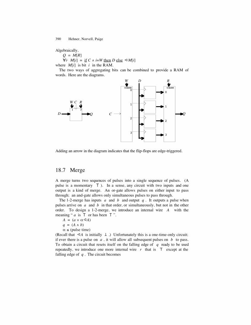
Algebraically,Q = M[R]∀i· M[i] = if C ∧ i=W then D else 4M[i]
where M[i] is bit i in the RAM.The two ways of aggregating bits can be combined to provide a RAM of
words. Here are the diagrams.
Q
W C
QC
0
1
2
3
case0
1
2
3
case
D
R
! ?
DW R
Adding an arrow in the diagram indicates that the flip-flops are edge-triggered.
18.7 Merge
A merge turns two sequences of pulses into a single sequence of pulses. (A pulse is a momentary † ). In a sense, any circuit with two inputs and one output is a kind of merge. An or-gate allows pulses on either input to pass through; an and-gate allows only simultaneous pulses to pass through.
The 1-2-merge has inputs a and b and output q . It outputs a pulse when pulses arrive on a and b in that order, or simultaneously, but not in the other order. To design a 1-2-merge, we introduce an internal wire A with the meaning “ a is † or has been † ”.
A = (a ∨ α4A)q = (A ∧ b)α ≤ (pulse time)
(Recall that 4A is initially ƒ .) Unfortunately this is a one-time-only circuit; if ever there is a pulse on a , it will allow all subsequent pulses on b to pass. To obtain a circuit that resets itself on the falling edge of q ready to be used repeatedly, we introduce one more internal wire r that is † except at the falling edge of q . The circuit becomes
390 Hehner, Norvell, Paige

r = (q ∨ ¬γ4q)A = (r ∧ (a ∨ α4A))q = (A ∧ b)α ≤ (pulse time) ∧ α ≤ γ
a
bq
q
a
b
A
r
a
g
1
2
Internal wires can be left exposed, as in the above specification of 1-2-merge and the right-hand diagram, or they can be hidden as in the left-hand diagram and the following specification:
∃r, A· r = (q ∨ ¬γ4q)∧ A = (r ∧ (a ∨ α4A))∧ q = (A ∧ b)
If a pulse on a follows a pulse on b , there must be a delay of at least γ after the end of b before the start of a to avoid truncating the output pulse. No circuit can constrain its inputs; its context of use must constrain its inputs, so a constraint is expressed formally as an antecedent rather than a conjunct. The circuit specification is therefore
¬(a ∧ ¬γ4a ∧ b)⇒ ∃r, A· r = (q ∨ ¬γ4q) ∧ A = (r ∧ (a ∨ α4A)) ∧ q = (A ∧ b)
A merge that outputs a pulse when the second of the two input pulses arrives, regardless of their order, and resets itself for reuse, is as follows. The inputs are a and b and the output is q . Internal wire A means “ a is † or has been † ”; internal wire B means “ b is † or has been † ”; internal wire r is † except at the falling edge of q . The circuit is
r = (q ∨ ¬γ4q)A = (r ∧ (a ∨ α4A))B = (r ∧ (b ∨ β4B))q = (A ∧ B ∧ (a ∨ b))α ≤ (pulse time) ∧ α ≤ γ ∧ β ≤ (pulse time) ∧ β ≤ γ
a
a
bq q
a
bB
A
r
b
g
18. High-level circuit design 391

18.8 Imperative circuits
The first of our two translations from programs to circuits produces “imperative” circuits (as in “imperative programming”). An imperative circuit has two components, an imperative control I , and a memory M , connected like this.
CσRσ Wσ
sI
M
s′
σ Dσ
!
!?
?
↓
The memory consists of a word for each global variable and a RAM for each global array in the program. (We present local variables later. By making variables as local as possible, we minimize the need for the global memory.) Suppose the variables are x and y , and the arrays are A and B . Then there are four clock wires, called Cx , Cy , CA , and CB , and collectively called Cσ . With one clock wire for each variable and each array, the variables and arrays can be independently and asynchronously changed. The data inputs are Dx , Dy , DA , and DB , collectively called Dσ . The address wires are W A , W B , RA , and RB , collectively called Wσ and Rσ . The memory outputs are x , y , A[RA] and B[RB] , collectively called σ , the state of memory. Altogether, memory is
M = ( x = (if ¬Cx ∧ 4Cx then 4Dx else 4x)∧ y = (if ¬Cy ∧ 4Cy then 4Dy else 4y)∧ (∀i· A[i] = if ¬CA ∧ 4CA ∧ i=WA then 4DA else 4A[i])∧ (∀i· B[i] = if ¬CB ∧ 4CB ∧ i=WB then 4DB else 4B[i]) )
We mention again that we are depicting logic, not layout; the best place for a bit of memory may be with a part of the control that uses it.
The state is input to the control, along with an initiator wire s . A pulse on s starts the computation. As the computation progresses, the control changes the state of memory, thus providing itself with further input. To change the value of variable x in memory, the control must send a pulse on clock wire Cx and the desired new value on wire Dx . If the computation is finite, then when it is complete, the control indicates termination by a pulse on the completion wire s′ . It is the responsibility of the context to ensure that the control is not restarted before it has completed an execution.
A program is sometimes composed of smaller programs. (In other terminology, a statement is sometimes composed of smaller statements; we do not distinguish between “program” and “statement”.) When a program is composed of parts, the control will be composed of the controls for the parts. To make the composition easy, we require of each part that its output Dx be ƒ at any instant when it is not changing variable x . Then we can disjoin the Dx wires on their way to memory. Other variables and arrays are similar. Here
392 Hehner, Norvell, Paige

is the diagram:
IQ
M
IP
!
!
!
?
?
?↓
Each disjunction is really many disjunctions, one for each bit in its operands.It is not our intention to present a new programming language for circuit
design; we advocate using a standard programming language. We next describe the control for a sampling of programming constructs from typical imperative languages.
Construct: empty
We begin with the simplest program: ok (sometimes called skip ). It is the “empty” program, whose execution does nothing, taking no time. Program ok yields the control
s′=s ∧ ¬Rσ ∧ ¬Cσ ∧ ¬Wσ ∧ ¬DσIts diagram is
ƒ
s s′σ Dσ
CσWσRσ
We have shown all its inputs and outputs. But since the σ input is not connected to anything, there is no point in bringing those wires from memory. And since the Rσ , Cσ , Wσ , and Dσ outputs are ƒ , there is no point in taking them into a disjunction. So the circuit reduces to nothing, which is appropriate for a circuit that does nothing.
Construct: delay
The next simplest program is tick , which also does nothing, but takes time δ to do it.
s′=δ4s ∧ ¬Rσ ∧ ¬Cσ ∧ ¬Wσ ∧ ¬Dσ
18. High-level circuit design 393
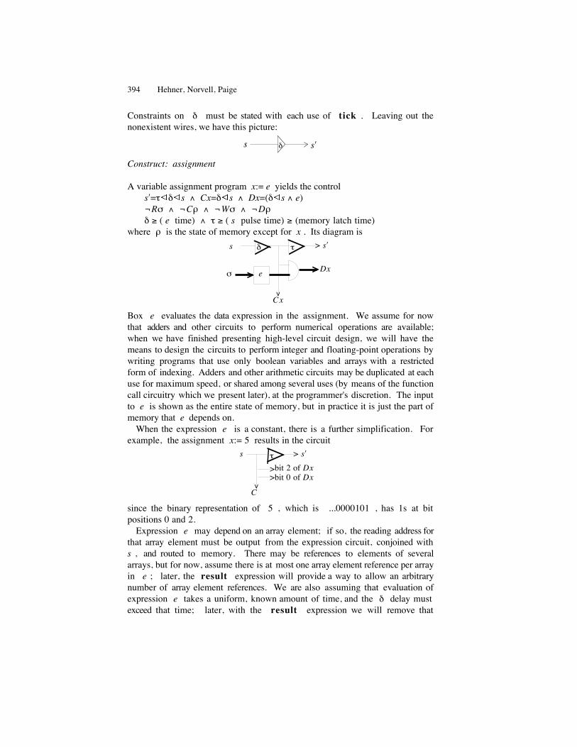
Constraints on δ must be stated with each use of tick . Leaving out the nonexistent wires, we have this picture:
s′δs
Construct: assignment
A variable assignment program x:= e yields the controls′=τ4δ4s ∧ Cx=δ4s ∧ Dx=(δ4s ∧ e)¬Rσ ∧ ¬Cρ ∧ ¬Wσ ∧ ¬Dρδ ≥ ( e time) ∧ τ ≥ ( s pulse time) ≥ (memory latch time)
where ρ is the state of memory except for x . Its diagram is
s′τδs
e
Cx
Dxσ
∨
> >
>
Box e evaluates the data expression in the assignment. We assume for now that adders and other circuits to perform numerical operations are available; when we have finished presenting high-level circuit design, we will have the means to design the circuits to perform integer and floating-point operations by writing programs that use only boolean variables and arrays with a restricted form of indexing. Adders and other arithmetic circuits may be duplicated at each use for maximum speed, or shared among several uses (by means of the function call circuitry which we present later), at the programmer's discretion. The input to e is shown as the entire state of memory, but in practice it is just the part of memory that e depends on.
When the expression e is a constant, there is a further simplification. For example, the assignment x:= 5 results in the circuit
τ s′s
C
bit 0 of Dxbit 2 of Dx
∨
>
>>
since the binary representation of 5 , which is ...0000101 , has 1s at bit positions 0 and 2.
Expression e may depend on an array element; if so, the reading address for that array element must be output from the expression circuit, conjoined with s , and routed to memory. There may be references to elements of several arrays, but for now, assume there is at most one array element reference per array in e ; later, the result expression will provide a way to allow an arbitrary number of array element references. We are also assuming that evaluation of expression e takes a uniform, known amount of time, and the δ delay must exceed that time; later, with the result expression we will remove that
394 Hehner, Norvell, Paige

assumption.An array element assignment program A[i]:= e yields the control
s′=τ4δ4sCA=δ4s ∧ DA=(δ4s ∧ e) ∧ WA=(δ4s ∧ i)¬Rσ ∧ ¬Cρ ∧ ¬Wρ ∧ ¬Dρδ ≥ (e time) ∧ δ ≥ (i time) ∧ τ ≥ (s pulse time) ≥ (memory latch time)
where ρ is the state of memory except for A . Its diagram is
e
CA
DA
i
WA
σ
τδ s′s >
>
>
>
∨ ∨∨∨∨
Construct: sequential composition
To implement sequential composition P;Q we suppose that we already have the controls IP and IQ for programs P and Q . To avoid name clashes we systematically rename the inputs and outputs of IP by adding the subscript P , and similarly for IQ . Then the control for P;Q is
IP ∧ IQs=sP ∧ s′P=sQ ∧ s′Q=s′σP=σQ=σ
Rσ=(RσP∨RσQ) ∧ Cσ=(CσP∨CσQ) ∧ Wσ=(WσP∨WσQ) ∧ Dσ=(DσP∨DσQ)Diagrammatically, ignoring the connections between the controls and memory, we have
IP IQs ′s
Construct: parallel composition
To implement parallel composition P||Q we need to start both programs (operands of || are often called “processes”), and then merge the completion pulses. We suppose that we already have the controls IP and IQ for programs P and Q . To avoid name clashes we systematically rename the inputs and outputs of IP by adding the subscript P , and similarly for IQ . Then the control for P||Q is
IP ∧ IQ ∧ merges=sP=sQ ∧ a=s′P ∧ b=s′Q ∧ s′=qσP=σQ=σ
Rσ=(RσP∨RσQ) ∧ Cσ=(CσP∨CσQ) ∧ Wσ=(WσP∨WσQ) ∧ Dσ=(DσP∨DσQ)
18. High-level circuit design 395

Diagrammatically, ignoring the connections to memory, we have
IP
IQ
s′s
This implementation of parallel composition allows P and Q to access memory simultaneously. For the memory we have described, simultaneous access to different variables or arrays poses no problem. Even for the same variable, simultaneous reads are no problem. But simultaneously reading and writing the same variable, or two simultaneous writes to the same variable, have unpredictable results. Below we will introduce communication channels to allow programs to share information without memory contention.
Construct: conditional composition
To implement conditional composition if b then P else Q we suppose that we already have the controls IP and IQ for programs P and Q . To avoid name clashes we systematically rename the inputs and outputs of IP by adding the subscript P , and similarly for IQ . Then the control for if b then P else Q is
IP ∧ IQsP=(δ4s∧b) ∧ sQ=(δ4s∧¬b) ∧ s′=(s′P∨s′Q)σP=σQ=σRσ=(RσP∨RσQ) ∧ Cσ=(CσP∨CσQ) ∧ Wσ=(WσP∨WσQ) ∧
Dσ=(DσP∨DσQ)δ ≥ ( b time)
Diagrammatically, ignoring the connections between the controls and memory, we have
IP
IQ
s ′
s
bσ
thenelse
if
δ
The assumptions about b are the same as those about the expression in an assignment.
A one-tailed if b then P is just if b then P else ok . To make a circuit for a case program, the if circuit is generalized in the obvious way.
Construct: loop
To implement while b do P we suppose that we already have the control IP
396 Hehner, Norvell, Paige

for program P . To avoid name clashes we systematically rename the inputs and outputs of IP by adding the subscript P . The control for while b do P is
IPsP=(δ4(s∨s′P) ∧ b) ∧ s′=(δ4(s∨s′P) ∧ ¬b)σP=σ ∧ Rσ=RσP ∧ Cσ=CσP ∧ Wσ=WσP ∧ Dσ=DσPδ ≥ ( b time)
Diagrammatically, ignoring the connections between IP and memory, we have
IP
s′s
bσ
thenelse
if
δ
Again, the assumptions about expression b are the same as those about the expression in an assignment.
To implement repeat P until b we suppose that we already have the control IP for program P . To avoid name clashes we systematically rename the inputs and outputs of IP by adding the subscript P . Then the control for repeat P until b is
IPsP=(s ∨ δ4s′P ∧ ¬b) ∧ s′=(δ4s′P ∧ b)σP=σ ∧ Rσ=RσP ∧ Cσ=CσP ∧ Wσ=WσP ∧ Dσ=DσPδ ≥ ( b time)
Diagrammatically, ignoring the connections between IP and memory, we have
IP
s′s
bσ
thenelse
if
δ
Again, the assumptions about expression b are the same as those about the expression in an assignment.
Some programming languages include a loop with intermediate exits. Unlike the previous constructs, loop P and exit cannot be implemented in isolation, but must be implemented together. Ignoring the connections between IP and memory, the control for loop P is
IP
sfrom exits s′
and that for an exit is
s ′s to end of loop ƒ
The exit wire to s′ is shown only so that the circuit has the right inputs and
18. High-level circuit design 397

outputs, but in practice it is unnecessary. To see how this works, consider the following example.
loop (P ; if b then exit; Q ; if c then exit; R)Its circuit is
ƒ
s ′bσ
thenelse
if
IP
s ƒ
cσ
thenelse
if
IQ IR
Each exit consists of a wire leading from a “then” to the final disjunction, and a ƒ leading into a disjunction. These ƒ inputs and the disjunctions they lead into can be eliminated.
Now that we have loop and exit , we could have defined while and repeat as special cases.
Construct: local variable
To declare local variable z of type T with scope P we write var z: T· P . It simply adds another word of memory, which is used only within P . Formally, its control is
∃z, Cz, Dz· IPwhere IP is the control for P . Local declaration helps to locate the words of memory near the control circuitry that uses them. The diagram follows:
IP
s
σ
Cσ
s′
Rσ Wσ
DσDz
Czz
!?
↓
To declare local array A of size s and type T with scope P we write var A[s]: T· P . The size must be a compile-time constant. It simply adds another RAM, which is used only within P . There is another way to implement array declarations that is preferable in some circumstances. We can treat the declaration of array A[3] as syntactic sugar for the declaration of three variables A0 , A1 , A2 . We treat the data expression A[i] as sugar for case i of A0 | A1 | A2 , and the assignment A[i]:= e as sugar for case i of A0:= e | A1:= e | A2:= e . This implementation allows parallel access and update of array elements.
398 Hehner, Norvell, Paige
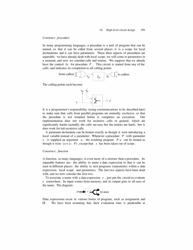
Construct: procedure
In many programming languages, a procedure is a unit of program that can be named, so that it can be called from several places; it is a scope for local declarations; and it can have parameters. These three aspects of procedures are separable; we have already dealt with local scope, we will come to parameters in a moment, and now we consider calls and returns. We suppose that we already have the control IP for procedure P . This circuit is started from any of the calls, and indicates its completion to all calling points.
P IP
from callers to callerss′Ps
The calling points each become
s′P
s′s
Ps
1
2
It is a programmer's responsibility (using communications to be described later) to make sure that calls from parallel programs are mutually exclusive, so that the procedure is not restarted before it completes an execution. Our implementation does not work for recursive calls in general, which are significantly harder (actually, the calls are easy but the returns are hard), but it does work for tail-recursive calls.
A parameter declaration can be treated exactly as though it were introducing a local variable instead of a parameter. Whenever a procedure P with parameter x is supplied an argument a , the resulting program P a can be treated as though it were (x:= a ; P) , except that x has been taken out of scope.
Construct: function
A function, in many languages, is even more of a mixture than a procedure. Its separable features are: the ability to name a data expression so that it can be used in different places; the ability to nest programs (statements) within a data expression; local scope; and parameters. The last two aspects have been dealt with, and we now consider the first two.
To associate a name with a data expression e , just put the circuit to evaluate e somewhere. Its input comes from memory, and its output goes to all uses of the name. The diagram:
eσ to uses
Data expressions occur in various forms of program, such as assignment and i f . We have been assuming that their evaluation time is predictable at
18. High-level circuit design 399

compile-time, but to be general, we allow circuits for data expressions to have a control line ( s input and s′ output). The data expression P result e requires execution of program P in order to create the correct state for evaluation of e . Its circuit inserts the appropriate delay in the control line. The delay may depend on the initial state, varying from one evaluation to another; it is not a worst-case delay. Its diagram is
IP
s
σ
s′
e P result e
CσRσ Wσ
Dσ? !
δ
where IP is the control for program P and δ ≥ ( e time) . If P changes only local variables, so that there are no side-effects, then the outputs Cσ, Wσ, Dσ to memory are unnecessary. Expression e should be evaluated in the local scope, so the input to e should include local variables as necessary. A result expression is often used as the body of a function. Another use is to help us out of an earlier difficulty: we were not allowed to have references to different elements of the same array within one basic data expression. But a compiler can transform an expression like A[i]+A[j] into
(var t: int· t:= A[i] result t+A[j])and so we now lift the earlier restriction.
Construct: communication
To declare local channel c of type T with scope P we write chan c: T· P . For one writing program and one reading program it is defined as follows.
(chan c: T· P) = (var c: T· var √c: bool· √c:= ƒ; P)It introduces two variables, called the buffer and the probe. The buffer c (same name as the channel) holds the value being communicated, and the probe √c (pronounced “check c ”) tells whether there is an unread message in the buffer. We define output of expression e and input to variable x on this channel as follows.
c! e = (while √c do tick; c:= e; √c:= †)c? x = (while ¬√c do tick; x:= c; √c:= ƒ)
Since we have already implemented all constructs on the right sides of these definitions, we therefore have implementations of channel declaration, input, and output. But there are two points that need attention. The tick delay must be longer than the control pulse (the pulse on s ) so the control pulse is not lost. And the while must use an edge-triggered switch so the control pulse will not be truncated, split, or otherwise damaged by a change in √c due to a parallel program. Although the buffer may also be shared by parallel programs that both read and write it, the discipline of use imposed by input and output ensures noninterference.
400 Hehner, Norvell, Paige

It may also be useful to introduce signals, which are messages without content. To declare local signal s with scope P we write sig s· P . For one sending program and one receiving program it is defined as follows:
(sig s· P) = (var √s: bool· √s:= ƒ; P)It introduces only the probe. We define sending and receiving this signal as follows.
s! = (while √s do tick; √s:= †)s? = (while ¬√s do tick; √s:= ƒ)
As before, the tick delay must be longer than the control pulse, and the while must use an edge-triggered switch. As examples of their use, we offer a second implementation of parallel programs. For each parallel composition P||Q we introduce a signal endP and the circuit is
IP
IQ
s′
sendP!
endP?
We can also use a signal to reimplement procedures. For each procedure P introduce signal endP and the circuit is
I P
from callers endP!
A call to P can be implemented as follows.
s′sendP?
to declaration
18.9 Functional circuits
The second of our two translations from programs to circuits produces “functional” circuits (as in “functional programming”). Functional circuits are not composed of a control and a memory; instead, each functional circuit computes its output σ′ from its input σ without the benefit of a separate memory (although some constructs will require internal memory). There is still a start signal s to initiate the computation and a stop signal s′ to indicate completion. Here's the diagram:
Fs′
σ′σ
s
The data input σ includes all variables and array elements. To use the circuit
18. High-level circuit design 401

we must provide the desired data input σ and a pulse (momentary † ) on the start wire s , and we must hold σ constant ever after (until the circuit is restarted). The functional circuit F must provide a correct data output σ′ and a pulse on the stop wire s′ , and it must hold σ′ constant ever after (until the circuit is restarted).
Construct: empty
For program ok the functional circuit is trivial, as it should be.
s ′σ′σ
s
Construct: assignment
A variable assignment x:= e looks like this:
σ
s′s
x′e
ρ′
where ρ′ is all variables and arrays other than x′ .Array element assignment A[i]:= e looks like this:
case
†
thenelse
if
A′[0]A [0]
thenelse
if
A′[1]A [1]
thenelse
if
A′[2]A [2]
thenelse
if
A′[3]A [3]
0
1
2
3
e
i
s′sρ′
σA
402 Hehner, Norvell, Paige

where ρ′ is all variables and arrays other than A′ .
Construct: sequential composition
Sequential execution is easy.
Fσ
sF
s′
σ′P Q
Construct: parallel composition
For parallel execution, we make the simplifying assumption that the parallel programs do not communicate via shared memory, but only via the communication constructs provided. The variables and array elements changed by one program are disjoint from those changed by a parallel program, and the changes made by one program are not seen by a parallel program.
F
σ
s
F
s′
σ′
P
Q
The entire input can go to both programs, but each program produces only part of the output. These outputs together form the entire output.
Construct: conditional composition
Here is the functional circuit for if b then P else Q .
FP
FQ
s′
σ
σ′
s
b
thenelse
if
The data output could, alternatively, be selected using the b output without memory.
The if circuit is easily generalized to a case circuit.
18. High-level circuit design 403

Construct: loop
Here is the functional circuit for loop P with exits in it:
FP s ′
σ
σ′
s
from exits
↓
↓
If there is only a single exit, the exit memory is unnecessary.Since while b do P is just loop (if b then P else exit) , its circuit is
σs FP
s′σ′
b
thenelse
if↓
↓
Similarly repeat P until b is just loop (P; if b then exit else ok).
Construct: local variable
The functional circuit for local variable declaration var z: T · P is particularly easy.
z
Fs s′
σ′Pσz′
Into the functional circuit for P we must feed data lines for z , with any desired initial value. The diagram shows the final value z′ coming from FP , but it is not wanted so its wires are not needed. A local array declaration is just like a local variable declaration; there is no extra circuitry needed here for access to elements.
Construct: procedure
Program declaration and calling work the same way in functional circuits as in imperative circuits, except that the data input must also come from the calling point, and the data output must be delivered back to the calling point. Like the imperative version, our functional implementation of procedures does not work for general recursion. Because the functional parallelism is disjoint, procedures cannot be called from parallel programs. For a procedure declaration we have the circuit
404 Hehner, Norvell, Paige

FP to callersfrom callers
and for each call we have the circuit
1
2
s
to declaration from declaration
σ′σ
s ′
Construct: function
Function declaration is similar to procedure declaration.
from callerse
to callers
Function call and return are identical to procedure call and return. The programmer must ensure that calls from parallel programs are mutually exclusive.
The data expression P result e is almost identical to the imperative circuit.
FP
s
σ
s ′
e P result e
The communication constructs are not given functional implementations for lack of truly shared memory in the parallel composition. For these constructs, we use hybrid circuits, described next.
18.10 Hybrid circuits
In general, functional circuits are faster than imperative circuits, but imperative circuits occupy less space. Each approach has merit. We can obtain almost the speed of a functional circuit with almost the compactness of an imperative circuit by combining the two kinds within one hybrid circuit. For example, we might make most of a circuit imperative, but make inner loops functional.
Hybrid circuits also allow us to use our imperative implementation of communication within a larger functional circuit.
To place a functional circuit within an imperative one, we must make the
18. High-level circuit design 405
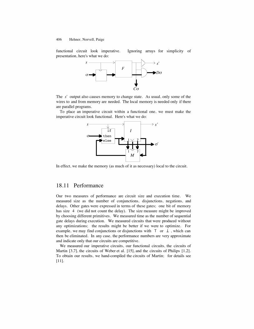
functional circuit look imperative. Ignoring arrays for simplicity of presentation, here's what we do:
F
s
σ
s′
Dσ
Cσ
The s′ output also causes memory to change state. As usual, only some of the wires to and from memory are needed. The local memory is needed only if there are parallel programs.
To place an imperative circuit within a functional one, we must make the imperative circuit look functional. Here's what we do:
s
I
M
s ′
σ′
σ thenelse
if
! ?
?!
In effect, we make the memory (as much of it as necessary) local to the circuit.
18.11 Performance
Our two measures of performance are circuit size and execution time. We measured size as the number of conjunctions, disjunctions, negations, and delays. Other gates were expressed in terms of these gates; one bit of memory has size 4 (we did not count the delay). The size measure might be improved by choosing different primitives. We measured time as the number of sequential gate delays during execution. We measured circuits that were produced without any optimizations; the results might be better if we were to optimize. For example, we may find conjunctions or disjunctions with † or ƒ , which can then be eliminated. In any case, the performance numbers are very approximate and indicate only that our circuits are competitive.
We measured our imperative circuits, our functional circuits, the circuits of Martin [3,7], the circuits of Weber et al. [15], and the circuits of Philips [1,2]. To obtain our results, we hand-compiled the circuits of Martin; for details see [11].
406 Hehner, Norvell, Paige

Our six test programs were chosen to use as many language features as possible. They are:
Parity: computes and verifies a parity bit for 3 bits of dataParallel: uses the parallelism and interprogram communication featuresArbiter: arbitration between two parallel programsCounter: a 4-bit binary countdown timer and test-and-set functionTriple: a program to compute three times its inputRing: mutually-exclusive execution of 7 parallel programs in a ring
using Peterson's algorithmA detailed description of the test programs and a similar analysis can be found in [11].
The results are listed in the following table.
TIME Parity Parallel Arbiter Counter Triple Ringimperative 16 31 165 1091 127 2321functional 16 25 113 799 90 3792Martin 18 23 209 1243 148 2044
SIZE Parity Parallel Arbiter Counter Triple Ringimperative 73 210 52 407 400 427functional 94 413 81 886 1240 1835Martin 98 123 76 431 385 357Weber et al. 259 145 95 1156 657 715Philips 96 196 79 810 597 940
18.12 Correctness
To prove that our circuits are correct, we must have a formal semantics for our source programs and circuits. Here is the source semantics.
Let t and t′ be the initial and final execution times, the times at which execution starts and ends. If the execution time is infinite, t′=∞ . Let the state variables x , y , ... be functions of time. The value of x at time t is x t . An expression such as x+y is also a function of time; its argument is distributed to its variable operands as follows: (x+y)t = x t + y t . Let
wait = (t′≥t ∧ ∀t′′: t≤t′′≤t′· xt′′=xt ∧ yt′′=yt ∧ ...)so that wait takes an arbitrary time during which the variables are unchanging.
The programming notations are defined as follows.ok = (t′=t)tick = (t′=t+δ ∧ wait)(x:= e) = (t′=t+δ+τ ∧ xt′=et ∧ waity,z...)
where δ ≥ ( e time) ∧ τ ≥ (memory time) .(P;Q) = ∃t′′· (substitute t′′ for t′ in P ) ∧ (substitute t′′ for t in Q )(Pα || Qβ) = (Pα ∧ (Q; wait)β ∨ (P; wait)α ∧ Qβ)
18. High-level circuit design 407

(if b then P else Q) = (if bt then P else Q) = (bt ∧ P ∨ ¬bt ∧ Q)
(while b do P) ⇒ if b then (P; while b do P) else ok(∀x, x′, y, y′, ..., t, t′· W ⇒ if b then (P; W ) else ok)
⇒ (∀x, x′, y, y′, ..., t, t′· W ⇒ while b do P)var z: T· P = ∃z: time→T· P
where time→T is the functions from time values (including ∞ ) to T values.Here is a simple example, in variables x and y . In this example we use
discrete time and take δ to be 0 and τ to be 1 .x:= x+3; x:= x+4
= (t′=t+1 ∧ xt′=xt+3 ∧ yt′=yt); (t′=t+1 ∧ xt′=xt+4 ∧ yt′=yt)= ∃t′′· (t′′=t +1 ∧ xt′′=xt+3 ∧ yt′′=yt) ∧ (t′=t′′+1 ∧ xt′=xt′′+4 ∧ yt′=yt′′)= t′=t+2 ∧ x(t+1)=xt+3 ∧ x(t+2)=xt+7 ∧ yt=y(t+1)=y(t+2)
In the parallel composition, α consists of those variables that appear on the left of assignments within P , and β consists of those variables that appear on the left of assignments within Q ; α and β must be disjoint. The use of wait is just to make the faster side of the parallel composition wait until the slower side is finished. To illustrate the semantics, here is an example in variables x and y , and discrete time with δ=0 and τ=1 . In the left-hand program, only x is assigned, so only x is treated as a state variable. In the right-hand program, only y is assigned, so only y is treated as a state variable.
(x:= 2; x:= x+y; x:= x+y) || (y:= 3; y:= x+y)= (t′ = t +1 ∧ xt′=2; t′ = t+1 ∧ xt′ = xt+yt; t′ = t+1 ∧ xt′ = xt+yt)
∧ (t′ = t +1 ∧ yt′=3; t′=t+1 ∧ yt′ = xt+yt; t′≥t ∧ ∀t′′: t≤t′′≤t′· yt′′=yt)
∨ (t′ = t +1 ∧ xt′=2; t′ = t+1 ∧ xt′ = xt+yt; t′ = t+1 ∧ xt′ = xt+yt; t′≥t ∧ ∀t′′: t≤t′′≤t′· xt′′=xt)
∧ (t′ = t +1 ∧ yt′=3; t′=t+1 ∧ yt′ = xt+yt)= t′=t+3 ∧ x(t+1)=2 ∧ x(t+2)=x(t+1)+y(t+1) ∧ x(t+3)=x(t+2)+y(t+2)
∧ t′≥t+2 ∧ y(t+1)=3 ∧ y(t+2)=x(t+1)+y(t+1)∧ ∀t′′: t+2≤t′′≤t′· yt′′=y(t+2))
∨ t′ ≥ t+3 ∧ (other conjuncts)∧ t′ = t+2 ∧ (other conjuncts)
= t′=t+3 ∧ x(t+1)=2 ∧ y(t+1)=3 ∧ x(t+2)=5 ∧ y(t+2)=5∧ x(t+3)=10 ∧ y(t+3)=5
The example has the appearance of lock-step parallelism, as though there were a global clock, only because, for the sake of simplicity, we used discrete time with constants δ=0 and τ=1 for all assignments.
The first formula concerning the while loop says that it refines its first unrolling. Stated differently, while b do P is a pre-fixed-point of
W ⇒ if b then (P; W ) else o kThe second formula says that it is as weak as any pre-fixed-point, so it is the weakest pre-fixed-point.
408 Hehner, Norvell, Paige

The other programming constructs (channel declaration, input, output, signal declaration, sending, receiving, parameter declaration, argumentation) are defined in terms of the ones we have already defined, so we do not need to give them a separate semantics. And that completes the source semantics.
The imperative circuit semantics was given with each circuit. For example, the control for ok was
s′=s ∧ ¬Rσ ∧ ¬Cσ ∧ ¬Wσ ∧ ¬Dσand the control for while b do P was
IPsP=(δ4(s∨s′P) ∧ b) ∧ s′=(δ4(s∨s′P) ∧ ¬b)σP=σ ∧ Rσ=RσP ∧ Cσ=CσP ∧ Wσ=WσP ∧ Dσ=DσPδ ≥ ( b time)
where IP is the control for P .Before we can prove correctness, we need one more idea, adapted from [9].
Roughly speaking, a circuit is “busy” if it has been started and has not yet stopped. Formally, define B as
B = ((s ∨ δ4B) ∧ ¬s′)δ ≤ (pulse time)
The delay here must be shorter than the pulse length used on the control lines ( s and s′ ). If time is discrete and δ=1 , then for any A
(4A) 0 = ƒ(4A) (t+1) = At
and so for busy BB0 = ƒB(t+1) = ((s(t+1) ∨ Bt) ∧ ¬s′(t+1))
To prove that a circuit is correct, we must prove IP ∧ M ∧ st ∧ (∀t′′· Bt′′∧4Bt′′ ⇒ ¬st′′) ∧ t′=(min t′′· t′′≥t· ∧ s′t′′) ⇒ P
Suppose we have the control IP (for program P ), and we have the memory M , and we put a pulse on the start wire s at time t , and we don't try to restart the circuit while it's busy, and we give the name t′ to the first time at or after t when s′ becomes † ; then we expect the circuit to satisfy the semantics of program P . We do not have to prove correct each circuit that we design; instead, we prove that our circuit generation scheme is correct. The proof is long, and we omit it, stating only two lemmas that are useful steps on the way to the proof:
I ∧ ¬4B ∧ ¬s ⇒ ¬s′which says that a circuit does not spontaneously generate s′ , and
I ∧ ¬B ⇒ ¬Rσ ∧ ¬Cσ ∧ ¬Wσ ∧ ¬Dσwhich says that if a circuit is not busy, its Rσ , Cσ , Wσ , and Dσ outputs are all ƒ .
18. High-level circuit design 409

18.13 Synchronous and asynchronous circuits
There are two ways to control the timing in circuits. One is by using delays calculated, or experimentally determined, to be long enough to ensure that all data values have settled properly. The other way, called “delay-insensitive”, is to use handshaking signals that allow a data transfer to occur just when both sender and receiver are ready. These solutions can be applied locally, or globally, or at any level in between. The word “synchronous” is usually used to describe a global delay, or clock; the word “asynchronous” is sometimes used to describe local handshaking.
The circuits resulting from the methods we have presented use local delays. But as a special case, it is possible to write a program in the form of a single loop, whose body is a parallel composition of assignments.
loop (x:= ex || y:= ey || z:= ez || ...)This program structure forces a single, common delay for all state changes; that delay is in effect a global clock. We can thus program a synchronous circuit when we want one. When designing a circuit, there is little point in aiming for the synchronous structure, and equally little point in aiming to avoid it. One chooses a program structure that is appropriate for the task, and one gets a circuit that accomplishes that task. In principle, local delays should be faster than a single global delay. That is because a global delay must be the maximum of all the local delays. In a synchronous circuit, each state change takes as long as the slowest state change requires.
If we choose to make each assignment into a little procedure, the 1-2-merges at the calling points are an implementation of local handshaking. We can thus program local handshaking when we want it. In principle, local delays should be faster than local handshaking. That is because the handshaking takes time. A local delay is just long enough for the data to be ready, not long enough for the data to be ready and to indicate its readiness.
18.14 Conclusions
Circuit design can be done more effectively by describing the function that a circuit is intended to perform than by describing a circuit that is intended to perform that function. A programming language is more convenient for that purpose than a gate-level language. It seems quite obvious that complex circuits can be designed this way more easily and reliably than by low-level gate descriptions. And the resulting circuits seem, from a preliminary investigation, to show the promise of competing successfully with hand-crafted circuits. They should be smaller and faster than synchronous circuits due to the absence of a global clock. They should also be smaller and faster than delay-insensitive circuits due to the absence of handshaking. These gains come at a price: the language implementer must provide local delays. We do not suppose it is easy
410 Hehner, Norvell, Paige

to provide local delays, but this price is paid only once; circuit designers who use the high-level language do not need to be concerned with them.
We have compiled a sampling of programming constructs that are representative of many high-level languages. Some obviously desirable constructs, such as modules, are missing only because they do not present any circuit generation problems (modules restrict the use of identifiers). For programs that we compiled and simulated, and for the text of the simulators, see [11].
We have shown two ways to implement ordinary programs with logic gates. The logic gates can, of course, be implemented with electronic transistors, resistors, and diodes. We could therefore bypass the logic gates, implementing the programs directly with transistors, resistors, and diodes. Doing so makes more optimizations and more efficient circuits possible. Ultimately, perhaps logic gates will have no remaining role in circuit design.
Acknowledgments
This paper was written in 1994 and circulated privately. We received useful feedback from IFIP WG2.3, and a lot of help from Jan van de Snepscheut.
References
[1] C.H.vanBerkel, J.Kessels, M.Roncken, R.W.J.J.Saeijs, F.Schalij. The VLSI programming language Tangram and its translation into handshake circuits. In Proceedings of the European Design Automation Conference, 1991.
[2] C.H.vanBerkel. Handshake circuits – an asynchronous architecture for VLSI programming. Cambridge University Press, 1993.
[3] S.M.Burns, A.J.Martin. Performance analysis and optimization of asynchronous circuits. In Proceedings of the 1991 UC Santa Cruz Conference on VLSI, MIT Press, 1991.
[4] C.DelgadoKloos. Semantics of Digital Circuits, Lecture Notes in Computer Science volume 285, Springer, 1987.
[5] E.C.R.Hehner. Abstractions of Time. In A Classical Mind: Essays in Honour of C.A.R.Hoare, A.W. Roscoe (ed.), Prentice-Hall, 1994.
18. High-level circuit design 411

[6] W.Luk, D.Ferguson, I.Page. Structured Hardware Compilation of Parallel Programs. In More Field-Programmable Gate Arrays, W.Moore and W.Luk (eds.), Abingdon EE&CS Books, 1994.
[7] A.J.Martin. Programming in VLSI: from communicating processes to delay-insensitive circuits. In Developments in Concurrency and Communication, C.A.R.Hoare (ed.), University of Texas at Austin Year of Programming Series, Addison-Wesley, 1990.
[8] S.Mazor, P.Langstraat. a Guide to VHDL, Kluwer, 1992.
[9] T.S.Norvell. a Predicative Theory of Machine Languages and its Application to Compiler Correctness. PhD thesis, University of Toronto, 1994.
[10] I.Page, W.Luk. Compiling occam into field-programmable gate arrays. In Field-Programmable Gate Arrays, W.Moore and W.Luk (eds.), p.271-283, Abingdon EE&CS Books, 1991.
[11] R.F.Paige. Correctness and Performance Analysis of Imperative and Functional Circuits. MSc thesis, University of Toronto, 1994.www.cs.yorku.ca/~paige/Writing/MSc.dvi
[12] M.Rem. Partially Ordered Computations with Applications to VLSI Design, Technical Report MR83/3, Eindhoven University of Technology, 1982
[13] J.L.A.van de Snepscheut. Trace Theory and VLSI Design, Lecture Notes in Computer Science volume 200, Springer, 1985.
[14] D.E.Thomas, P.Moorby. the Verilog Hardware Description Language, Kluwer, 1991.
[15] S.Weber, B.Bloom, G.Brown. Compiling Joy into Silicon. In Advanced Research in VLSI and Parallel Systems, T. Knight and J. Savage (eds.), MIT Press, 1992.
412 Hehner, Norvell, Paige