high frequency secondary rectifier - home - … frequency secondary rectifier datasheet - production...
TRANSCRIPT
June 2015 DocID5377 Rev 11 1/17
This is information on a product in full production. www.st.com
STTH2003
High frequency secondary rectifier
Datasheet - production data
Features Combines highest recovery and reverse
voltage performance
Ultra-fast, soft and noise-free recovery
Insulated package: TO-220FPAB
Insulating voltage = 2000 VRMS sine
ECOPACK®2 compliant component for D²PAK on demand
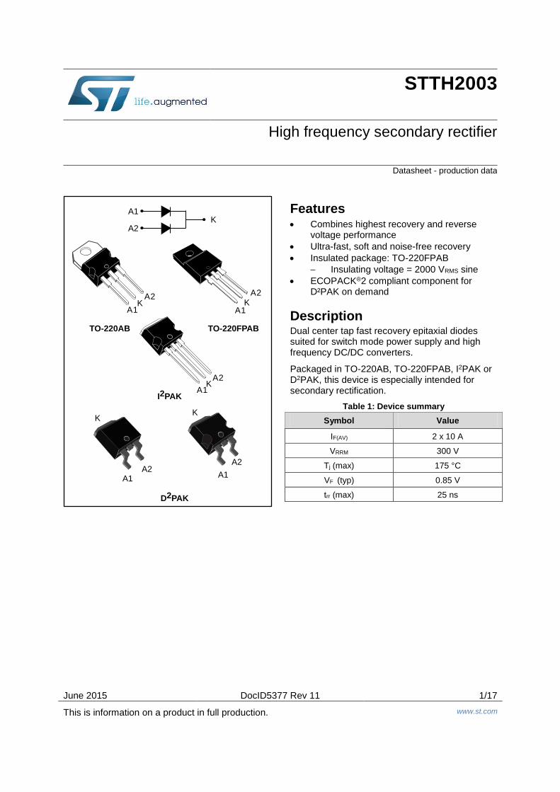
Description Dual center tap fast recovery epitaxial diodes suited for switch mode power supply and high frequency DC/DC converters.
Packaged in TO-220AB, TO-220FPAB, I2PAK or D2PAK, this device is especially intended for secondary rectification.
Table 1: Device summary
Symbol Value
IF(AV) 2 x 10 A
VRRM 300 V
Tj (max) 175 °C
VF (typ) 0.85 V
trr (max) 25 ns
KK
A1 A1A2
A2
D2PAK
A1K
A2
A1K
A2
TO-220AB
A1K
A2
TO-220FPAB
A1K
A2
I2PAK
Characteristics STTH2003
2/17 DocID5377 Rev 11
1 Characteristics Table 2: Absolute ratings (limiting values, per diode, at 25 °C, unless otherwise specified)
Symbol Parameter Value Unit
VRRM Repetitive peak reverse voltage 300 V
IF(RMS) Forward rms current 30 A
IF(AV)
Average forward
current δ = 0.5,
square wave
TO-220AB, D2PAK,
I2PAK TC = 140 °C Per
diode 10
A TO-220FPAB TC = 115 °C
All types Per device 20
IFSM
Surge non
repetitive forward
current
tp = 10 ms sinusoidal 110 A
Tstg Storage temperature range -65 to + 175 °C
Tj Maximum operating junction temperature (1) + 175 °C
Notes:
(1)(dPtot/dTj) < (1/Rth(j-a)) condition to avoid thermal runaway for a diode on its own heatsink.
Table 3: Thermal parameter
Symbol Parameter Value Unit
Rth(j-c) Junction to case
TO-220AB, D2PAK, I2PAK Per diode
2.5
°C/W TO-220FPAB 4.6
TO-220AB, D2PAK, I2PAK Total
1.3
TO-220FPAB 4
Rth(c) Coupling TO-220AB, D2PAK, I2PAK
- 0.1
°C/W TO-220FPAB 3.5
When the diodes 1 and 2 are used simultaneously:
ΔTj (diode1) = P(diode1) x Rth(j-c) (per diode) + P(diode2) x Rth(c)
Table 4: Static electrical characteristics (per diode)
Symbol Parameter Test conditions Min. Typ. Max. Unit
IR(1) Reverse leakage current Tj = 25 °C
VR = 300 V -
20
µA Tj = 125 °C - 30 300
VF(2) Forward voltage drop
Tj = 25 °C IF = 10 A
-
1.25 V
Tj = 125 °C - 0.85 1
Notes:
(1)Pulse test: tp = 5 ms, δ < 2% (2)Pulse test: tp = 380 µs, δ < 2%

STTH2003 Characteristics
DocID5377 Rev 11 3/17
To evaluate the conduction losses use the following equation:
P = 0.75 x IF(AV) + 0.025 IF2(RMS)
Table 5: Recovery characteristics (per diode)
Symbol Parameter Test conditions Min. Typ. Max. Unit
trr Reverse recovery time
Tj= 25 °C
IF= 0.5 A, Irr= 0.25 A, IR= 1 A -
25
ns IF= 1 A, VR= 30 V,dIF/dt= -50 A/µs
-
35
tfr Forward recovery time
Tj= 25 °C
IF= 10 A, VFR= 1.1 x VFmax, dIF/dt= 100 A/µs
-
230 ns
VFP Peak forward voltage
Tj= 25 °C
IF= 10 A, dIF/dt= 100 A/µs -
3.5 V
IRM Reverse recovery
current Tj= 125 °C
IF= 10 A, VCC= 200 V, dIF/dt= 200 A/µs
-
8 A
S factor Softness factor - 0.3
-
1.1 Characteristics (curves)
Figure 1: Conduction losses versus average forward current (per diode)
Figure 2: Forward voltage drop versus forward current (maximum values, per diode)
Figure 3: Relative variation of thermal impedance junction to case versus pulse duration (TO-220AB,
D²PAK, I²PAK)
Figure 4: Relative variation of thermal impedance junction to case versus pulse duration (TO-
220FPAB)
0 2 4 6 8 10 12
0
2
4
6
8
10
12
14
P1(W)
T
δ=tp/T tp
δ = 0.05
δ = 1
I (A)F(AV)
δ = 0.1 δ = 0.2 δ = 0.5
1E-3 1E-2 1E-1 1E+0
0.0
0.2
0.4
0.6
0.8
1.0
Z /Rth(j-c ) th(j-c)
t (s)p
Single pulse
1E-2 1E-1 1E+0 1E+1
0.0
0.2
0.4
0.6
0.8
1.0
Z /Rth(j-c ) th(j-c)
t (s)p
Single pulse

Characteristics STTH2003
4/17 DocID5377 Rev 11
Figure 5: Peak reverse recovery current versus dIF/dt (typical values, per diode)
Figure 6: Reverse recovery time versus dIF/dt (typical values, per diode)
Figure 7: Softness factor versus dIF/dt (typical values, per diode)
Figure 8: Relative variation of dynamic parameters versus junction temperature (reference: Tj = 125
°C)
Figure 9: Transient peak forward voltage versus dIF/dt (typical values, per diode) (TO-220AB)
Figure 10: Forward recovery time versus dIF/dt (typical values, per diode)
0 50 100 150 200 250 300 350 400 450 500
0
2
4
6
8
10
12
14
16I (A)RM
dI /dt(A/µs)F
I =2 x IF F(AV)
I =IF F(AV)
I =0.5 x IF F(AV)
V =200V
T =125°CR
j
0 50 100 150 200 250 300 350 400 450 500
0
20
40
60
80
100
t (ns)rr
dI /dt(A/µs)F
I =2 x IF F(AV)
I =IF F(AV)
I =0.5 x IF F(AV)
V =200V
T =125°CR
j
0 50 100 150 200 250 300 350 400 450 500
0.00
0.10
0.20
0.30
0.40
0.50
0.60
S factor
dI /dt(A/µs)F
V =200V
T =125°CR
j
0 50 100 150 200 250 300 350 400 450 500
0
2
4
6
8
10
V (V)FP
dI /dt(A/µs)F
I =I
T =125°CF F(AV)
j
0 50 100 150 200 250 300 350 400 450 500
0
100
200
300
400
500t (ns)fr
dI /dt(A/µs)F
I =I
T =125°C
F F(AV)
j
V =1.1 x V max.FR F

STTH2003 Characteristics
DocID5377 Rev 11 5/17
Figure 11: Thermal resistance, junction to ambient, versus copper surface under tab (epoxy printed
board FR4, eCu =35µm) (D²PAK)
Figure 12: Average forward current versus ambient temperature (δ = 0.5, per diode)
0
10
20
30
40
50
60
70
80
0 5 10 15 20 25 30 35 40
Rth
(j-a
)(°C
/W)
SCu(cm²)
0
1
2
3
4
5
6
7
8
9
10
11
12
0 25 50 75 100 125 150 175
I (A)F(AV)
T (°C)amb
R = Rth(j-a) th(j-c)
TO-220AB / I PAK / D PAK2 2
TO-220FPAB

Package information STTH2003
6/17 DocID5377 Rev 11
2 Package information
In order to meet environmental requirements, ST offers these devices in different grades of ECOPACK® packages, depending on their level of environmental compliance. ECOPACK® specifications, grade definitions and product status are available at: www.st.com. ECOPACK® is an ST trademark.
Cooling method: by conduction (C)
Epoxy meets UL 94,V0
Recommended torque value: 0.55 N·m (for TO-220AB and TO-220FPAB)
Maximum torque value: 0.7 N·m (for TO-220AB and TO-220FPAB)

STTH2003 Package information
DocID5377 Rev 11 7/17
2.1 D²PAK package information
Figure 13: D²PAK package outline
This package drawing may slightly differ from the physical package. However, all the specified dimensions are guaranteed.
Package information STTH2003
8/17 DocID5377 Rev 11
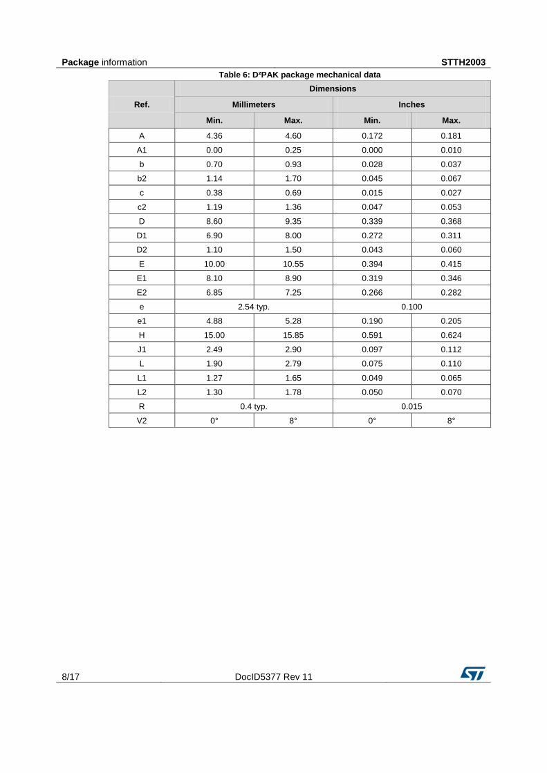
Table 6: D²PAK package mechanical data
Ref.
Dimensions
Millimeters Inches
Min. Max. Min. Max.
A 4.36 4.60 0.172 0.181
A1 0.00 0.25 0.000 0.010
b 0.70 0.93 0.028 0.037
b2 1.14 1.70 0.045 0.067
c 0.38 0.69 0.015 0.027
c2 1.19 1.36 0.047 0.053
D 8.60 9.35 0.339 0.368
D1 6.90 8.00 0.272 0.311
D2 1.10 1.50 0.043 0.060
E 10.00 10.55 0.394 0.415
E1 8.10 8.90 0.319 0.346
E2 6.85 7.25 0.266 0.282
e 2.54 typ. 0.100
e1 4.88 5.28 0.190 0.205
H 15.00 15.85 0.591 0.624
J1 2.49 2.90 0.097 0.112
L 1.90 2.79 0.075 0.110
L1 1.27 1.65 0.049 0.065
L2 1.30 1.78 0.050 0.070
R 0.4 typ. 0.015
V2 0° 8° 0° 8°

STTH2003 Package information
DocID5377 Rev 11 9/17
Figure 14: D²PAK recommended footprint (dimensions in mm)

Package information STTH2003
10/17 DocID5377 Rev 11
2.2 I²PAK package information
Figure 15: I²PAK package outline

STTH2003 Package information
DocID5377 Rev 11 11/17
Table 7: I²PAK package mechanical data
Ref.
Dimensions
Millimeters Inches
Min. Max. Min. Max.
A 4.40 4.60 0.173 0.181
A1 2.40 2.72 0.094 0.107
b 0.61 0.88 0.024 0.035
b1 1.14 1.70 0.044 0.067
F 0.75 1.0 0.03 0.039
F1 1.15 1.70 0.045 0.067
F2 1.15 1.70 0.045 0.067
G 4.95 5.20 0.195 0.205
G1 2.40 2.70 0.094 0.106
H 10.00 10.40 0.393 0.409
L2 16.00 typ. 0.63 typ.
L3 28.60 30.60 1.126 1.205
L4 9.80 10.6 0.386 0.417
L5 2.90 3.60 0.114 0.142
L6 15.90 16.40 0.626 0.646
L7 9.00 9.30 0.354 0.366
Dia 3.0 3.20 0.118 0.126
Mounting (soldering) the I2PAK metal slug (heatsink) with alloy, like a surface mount device, IS NOT PERMITTED. A standard through-hole mounting is mandatory.

Package information STTH2003
12/17 DocID5377 Rev 11
2.3 TO-220AB package information
Figure 16: TO-220AB package outline
A
C
D
L7
Dia
L5
L6
L9
L4
F
H2
G
G1
L2
F2
F1
EM

STTH2003 Package information
DocID5377 Rev 11 13/17
Table 8: TO-220AB package mechanical data
Ref.
Dimensions
Millimeters Inches
Min. Max. Min. Max.
A 4.40 4.60 0.173 0.181
C 1.23 1.32 0.048 0.051
D 2.40 2.72 0.094 0.107
E 0.49 0.70 0.019 0.027
F 0.61 0.88 0.024 0.034
F1 1.14 1.70 0.044 0.066
F2 1.14 1.70 0.044 0.066
G 4.95 5.15 0.194 0.202
G1 2.40 2.70 0.094 0.106
H2 10.00 10.40 0.393 0.409
L2 16.40 typ. 0.645 typ.
L4 13.00 14.00 0.511 0.551
L5 2.65 2.95 0.104 0.116
L6 15.25 15.75 0.600 0.620
L7 6.20 6.60 0.244 0.259
L9 3.50 3.93 0.137 0.154
M 2.6 typ. 0.102 typ.
Diam 3.75 3.85 0.147 0.151

Package information STTH2003
14/17 DocID5377 Rev 11
2.4 TO-220FPAB package information
Figure 17: TO-220FPAB package outline
H
A
B
Dia
L7
L6
L5
F1
F2
F
D
E
L4
G1
G
L2
L3

STTH2003 Package information
DocID5377 Rev 11 15/17
Table 9: TO-220FPAB package mechanical data
Ref.
Dimensions
Millimeters Inches
Min. Max. Min. Max.
A 4.40 4.60 0.173 0.181
B 2.5 2.7 0.098 0.106
D 2.50 2.75 0.098 0.108
E 0.45 0.70 0.018 0.027
F 0.75 1.0 0.03 0.039
F1 1.15 1.70 0.045 0.067
F2 1.15 1.70 0.045 0.067
G 4.95 5.20 0.195 0.205
G1 2.40 2.70 0.094 0.106
H 10.00 10.40 0.393 0.409
L2 16.00 typ. 0.63 typ.
L3 28.60 30.60 1.126 1.205
L4 9.80 10.6 0.386 0.417
L5 2.90 3.60 0.114 0.142
L6 15.90 16.40 0.626 0.646
L7 9.00 9.30 0.354 0.366
Dia 3.0 3.20 0.118 0.126

Ordering information STTH2003
16/17 DocID5377 Rev 11
3 Ordering information Table 10: Ordering information
Order code Marking Package Weight Base qty Delivery mode
STTH2003CT STTH2003CT TO-220AB 1.95g 50 Tube
STTH2003CG STTH2003CG D2PAK 1.38g 50 Tube
STTH2003CG-TR STTH2003CG D2PAK 1.38g 1000 Tape and reel
STTH2003CFP STTH2003CFP TO-220FPAB 1.9g 50 Tube
STTH2003CR STTH2003CR I2PAK 1.5g 50 Tube
4 Revision history Table 11: Document revision history
Date Revision Changes
Aug-2003 7G Previuous release
26-Mar-2007 8 Removed ISOWATT package
11-Feb-2011 9
Updatd base quantity for tape and reel delivery.
Corrected temperature in Table 1. Added warning paragraph above
Table 7.
06-Sep-2011 10 Updated Table 2. Added Figure 12
28-May-2015 11
Updated features, Table 1: "Device summary" and packages
silhouette in cover page.
Updated Section 1: "Characteristics".
Updated Section 2.2: "D²PAK package information".

STTH2003
DocID5377 Rev 11 17/17
IMPORTANT NOTICE – PLEASE READ CAREFULLY
STMicroelectronics NV and its subsidiaries (“ST”) reserve the right to make changes, corrections, enhancements, modifications , and improvements to ST products and/or to this document at any time without notice. Purchasers should obtain the latest relevant information on ST products before placing orders. ST products are sold pursuant to ST’s terms and conditions of sale in place at the time of order acknowledgement.
Purchasers are solely responsible for the choice, selection, and use of ST products and ST assumes no liability for application assistance or the design of Purchasers’ products.
No license, express or implied, to any intellectual property right is granted by ST herein.
Resale of ST products with provisions different from the information set forth herein shall void any warranty granted by ST for such product.
ST and the ST logo are trademarks of ST. All other product or service names are the property of their respective owners.
Information in this document supersedes and replaces information previously supplied in any prior versions of this document.
© 2015 STMicroelectronics – All rights reserved