high frequency dc-dc ac-led driver based on zcs-qrcs · however, there is no factual evidence on...
TRANSCRIPT

High frequency dc-dc AC-LED driver based on ZCS-QRCs
Ignacio Castro, Sergio Lopez, Kevin Martin, Manuel Arias, Diego G. Lamar and Javier Sebastian Departamento de Ingeniería Eléctrica, Electrónica, de Computadores y Sistemas
University of Oviedo Gijón 33204, Spain
e-mail: [email protected]
Abstract— A boost dc-dc dimmable AC-LED driver is
presented in this paper based on Zero Current Switching Quasi-Resonant Converters (ZCS-QRCs). The proposed driver is based on replacing the diode in conventional converter topologies (i.e. buck, boost or buck-boost) by a string of High-Brightness Light-Emitting Diodes (HB-LED). Hence, the HB-LED string will be working as the rectifier of the converter switching at the same frequency of the main switch. In this case, the output current, which is experimentally validated, shows a negative current peak due to the reverse recovery effect of the HB-LEDs. In order to reduce said effect on the HB-LEDs, the main switch of the proposed topologies is replaced with a full-wave resonant switch, which makes possible to reduce the di/dt during the turn-off of the HB-LED string, therefore the reverse recovery effect is minimized. Moreover, the dimming of the HB-LEDs is done by means of changing the switching frequency of the converter by varying the turn-off, while keeping a constant turn-on time. The proposed driver is suggested to be used in a post-regulator stage of an ac-dc converter or as the interface between the low voltage bus and the HB-LED string in a dc nanogrid. In order to validate the analysis, the proposed topologies have been experimentally tested on a dc-dc, AC-LED, ZCS-QRC, boost converter with an output power of 7.5 W constructed prototype, that is able to achieve a luminous efficacy of 110 lm/W at full load
Keywords—LED driver, AC-LED, ZCS-QRC, boost.
I. INTRODUCTION High-Brightness Light-Emitting Diodes (HB-LED) are
increasingly becoming our main source of artificial light in our homes, offices or streets due to their reliability, long lifetime, energy efficiency and low maintenance requirements. However, HB-LEDs are diodes, which means that the current is able to go through them in only one direction. This feature has made the driving of HB-LEDs from the mains an important research topic for a wide range of power [1]. For this reason, it is required the use of an ac-dc converter, specifically for output powers higher than 25 W it needs to be able to achieve Power Factor Correction (PFC), that feeds the string of HB-LEDs with either a constant [2] or a low-frequency pulsed current in the range of hundreds to thousands of kHz [3]. Traditionally, an ac-dc HB-LED driver, when cost is not the main concern and reliability and efficiency are of more importance, uses a two-stage [4] or three-stage [5] approach. In fact, the last stage of the driver (i.e. second or third stage) is normally used for the sole purpose of dimming the HB-LEDs, which is traditionally achieved by lowering the mean value of the output current. In this case, the last stage is also referred as a post-regulator. This post-regulator stage needs to
be cheap and achieve both high efficiency and high power density [6].
The idea presented in this work is based on using the basic dc-dc converter topologies (i.e. buck, boost and buck-boost), which are depicted in Fig. 1 (a), (d) and (g) and replace their diode D1 with the string of HB-LEDs while short-circuiting their output. As a result, two different converters can be obtained: LED paralleled with Switch (DL//S, i.e. Fig. 1 (e)) and LED paralleled with Inductor (DL//L, i.e. Fig. 1 (b) and (h)). It should be noted, that while in conventional buck, boost and buck-boost converters, the HB-LEDs are supplied with a constant current, in DL//S and DL//L, the HB-LED string is supplied with a pulsed current, pulsing at the same frequency at which the main switch (i.e. S1) is operating. The operation of HB-LEDs at high frequencies (i.e. > 100 kHz) acting as the regular diodes of a power converter, also referred in literature as high-frequency AC-LED driving, has been studied by means of resonant dual half bridges applying a sinusoidal high frequency current waveform to the HB-LEDs [7]-[9]. However, there is no factual evidence on how will the HB-LEDs perform under a high frequency sinusoid current waveform in terms of light quality, reliability or Correlated Color Temperature (CCT).
Following the same concept, some studies have been dedicated to the driving of white HB-LEDs (i.e. PWM dimming) under different current waveforms (i.e. sinusoidal, square and triangular) at 50 Hz [10] or up to 300 kHz with square waveforms [11]. Some important conclusions can be drawn from this works. First, the increase of frequency in a square current waveform from 100 Hz to 300 kHz does not have a negative impact on either the junction temperature or the light efficiency. Second, pulsed current is actually better for white HB-LEDs in terms of degradation over time. Third, the pulsed current technique is also regarded as a better driving technique than constant current in terms of chromaticity shifts [12]. And fourth, the switching of HB-LEDs at higher frequencies than 3 kHz presents no visible flicker or harmful effects to the viewers [13].
Regarding the previous facts, it is necessary to understand how well would an HB-LED operate as a diode due to the lack of dynamic characterization of white HB-LEDs in the manufacturer datasheets. In previous literature, some studies have characterized the frequency response of white HB-LEDs for Visible Light Communications (VLC) [14], showing a bandwidth of up to 3 MHz. However, this study does not add any information on how fast can the LED truly switch. Therefore, a study to characterize the HB-LED string under high
This work has been supported by the Spanish Government under Project MINECO-13-DPI2013-47176-C2-2-R and the Principality of Asturias under the grants “Severo Ochoa” BP14-140 and BP14-85 and by the Project FC-15-GRUPIN14-143 and by European Regional Development Fund (ERDF) grants.

frequency switching operation in power converters needs to be performed to observe, whether the well-known phenomena of reverse recovery [15] could occur in the proposed topologies. Considering the reverse-recovery effect could occur on the HB-LEDs, the di/dt during the turn-off of the HB-LED needs to be lowered to eliminate it. The di/dt reduction can be performed by either increasing the count of switches [16], which is not desirable, or by means of a Zero-Current-Switched Quasi-Resonant Converter (ZCS-QRC). The ZCS-QRC will be obtained by replacing the main switch of DL//L and DL//S with the full wave resonant switch [17]-[20]. This renders two converters: DL//L ZCS-QRC (i.e. Fig. 1 (c) and (i)) and DL//S ZCS-QRC (i.e. Fig. 1 (f)).
The proposal of this work is for these converters to be used as a post-regulator when driving HB-LEDs from the mains or as the required interface between the low voltage bus and one of the several strings of HB-LEDs that can be present in a dc nanogrid [21]. Moreover, the dimming of the HB-LEDs is done by means of changing the switching frequency of the converter, by varying the turn-off and keeping a constant turn-on time in the main switch.
Summarizing, this work analyses the working principle, from a static point of view, for ZCS-QRC DL//S is carried out in Section II. In order to validate the analysis a prototype has been constructed an experimentally validated with its results summarized in Section III. In this section, the results of a reliability test that has been carried out for 700 h comparing a conventional boost, a DL//S and a DL//S ZCS-QRC are also summarized. Finally, some conclusions are drawn in Section IV from the experimental results.
II. WORKING PRINCIPLE The concept of the dc-dc HB-LED drivers presented in this
work is based on using the HB-LEDs as the output diode of a dc-dc converter with a full-wave resonant switch. The main reason for using a full-wave resonant switch instead of a half-
wave resonant switch, is based on one of the key characteristics that this driver needs to have, which is the ability to achieve full dimming. It is a well-known fact, that the input/output relationship of a half-wave ZCS-QRC varies greatly with the load. In a driver in which the output current will be varying from zero to maximum current to meet the driving requirements, this fact will complicate unnecessarily its control. Hence, this analysis is only going to be considered for full-wave resonant switches which show next to no variation with its load.
In the forthcoming analysis the HB-LEDs are considered to be an ideal diode in series with their dynamic resistance (rLED) and their forward voltage (Vγ_LED).
It is also important to note that the main inductor (L1) is going to be considered much larger than the resonant inductor (Lr) in order for L1 not to affect the resonant frequency between Lr and the resonant capacitor (Cr), which is a well-known fact in ZCS-QRCs [17]. Moreover, in the case of the proposed topology, L1 needs to be large enough to satisfy that the current ripple is also as small as possible. Hence, being able to consider the output current as constant during the conduction of the HB-LEDs. This reason makes the increase of the switching frequency an attractive solution to diminish the size of L1, which will be the most limiting factor in terms of size in the proposed driver.
The resonant tank comprised by Lr and Cr, will resonate at,
𝜔𝜔𝑛𝑛 =1
�𝐿𝐿𝑟𝑟𝐶𝐶𝑟𝑟 , (1)
and the characteristic impedance is defined by,
𝑍𝑍𝑛𝑛 = �𝐿𝐿𝑟𝑟𝐶𝐶𝑟𝑟
. (2)
The operation of the HB-LED driver is summarized in Fig. 2, where the four equivalent circuits that the DL//S ZCS-QRC
Fig. 1. Basic converters. (a) Buck converter. (b) DL//L converter. (c) DL//L ZCS-QRC. (d) Boost converter. (e) DL//S converter. (f) DL//S ZCS-QRC. (g) Buck-
Boost converter. (h) DL//L converter. (i) DL//L ZCS-QRC.
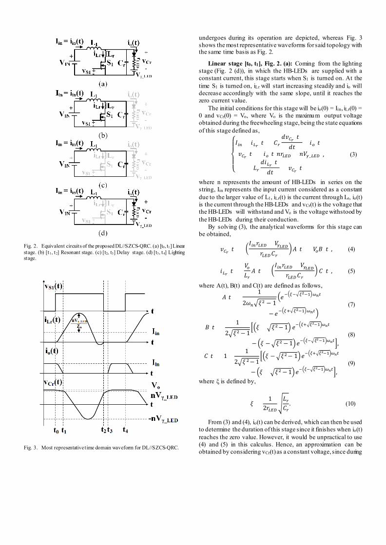
undergoes during its operation are depicted, whereas Fig. 3 shows the most representative waveforms for said topology with the same time basis as Fig. 2.
Linear stage [t0, t1], Fig. 2. (a): Coming from the lighting stage (Fig. 2 (d)), in which the HB-LEDs are supplied with a constant current, this stage starts when S1 is turned on. At the time S1 is turned on, iLr will start increasing steadily and io will decrease accordingly with the same slope, until it reaches the zero current value.
The initial conditions for this stage will be io(0) = Iin, iLr(0) = 0 and vCr(0) = Vo, where Vo is the maximum output voltage obtained during the freewheeling stage, being the state equations of this stage defined as,
⎩⎪⎨
⎪⎧𝐼𝐼𝑖𝑖𝑛𝑛 = 𝑖𝑖𝐿𝐿𝑟𝑟(𝑡𝑡) + 𝐶𝐶𝑟𝑟
𝑑𝑑𝑣𝑣𝐶𝐶𝑟𝑟(𝑡𝑡)𝑑𝑑𝑡𝑡
+ 𝑖𝑖𝑜𝑜(𝑡𝑡)
𝑣𝑣𝐶𝐶𝑟𝑟(𝑡𝑡) = 𝑖𝑖𝑜𝑜(𝑡𝑡)𝑛𝑛𝑟𝑟𝐿𝐿𝐿𝐿𝐿𝐿 + 𝑛𝑛𝑉𝑉𝛾𝛾_𝐿𝐿𝐿𝐿𝐿𝐿
𝐿𝐿𝑟𝑟𝑑𝑑𝑖𝑖𝐿𝐿𝑟𝑟(𝑡𝑡)𝑑𝑑𝑡𝑡
= 𝑣𝑣𝐶𝐶𝑟𝑟(𝑡𝑡)
, (3)
where n represents the amount of HB-LEDs in series on the string, Iin represents the input current considered as a constant due to the larger value of L1, iLr(t) is the current through Lr, io(t) is the current through the HB-LEDs and vCr(t) is the voltage that the HB-LEDs will withstand and Vo is the voltage withstood by the HB-LEDs during their conduction.
By solving (3), the analytical waveforms for this stage can be obtained,
𝑣𝑣𝐶𝐶𝑟𝑟(𝑡𝑡) = �𝐼𝐼𝑖𝑖𝑛𝑛𝑟𝑟𝐿𝐿𝐿𝐿𝐿𝐿 + 𝑉𝑉𝛾𝛾𝐿𝐿𝐿𝐿𝐿𝐿
𝑟𝑟𝐿𝐿𝐿𝐿𝐿𝐿𝐶𝐶𝑟𝑟�𝐴𝐴(𝑡𝑡) + 𝑉𝑉𝑜𝑜𝐵𝐵(𝑡𝑡), (4)
𝑖𝑖𝐿𝐿𝑟𝑟(𝑡𝑡) =𝑉𝑉𝑜𝑜𝐿𝐿𝑟𝑟𝐴𝐴(𝑡𝑡) + �
𝐼𝐼𝑖𝑖𝑛𝑛𝑟𝑟𝐿𝐿𝐿𝐿𝐿𝐿 + 𝑉𝑉𝛾𝛾𝐿𝐿𝐿𝐿𝐿𝐿𝑟𝑟𝐿𝐿𝐿𝐿𝐿𝐿𝐶𝐶𝑟𝑟
� 𝐶𝐶(𝑡𝑡), (5)
where A(t), B(t) and C(t) are defined as follows,
𝐴𝐴(𝑡𝑡) =1
2𝜔𝜔𝑛𝑛�𝜉𝜉2 − 1�𝑒𝑒−�𝜉𝜉−�𝜉𝜉
2−1�𝜔𝜔𝑛𝑛𝑡𝑡
− 𝑒𝑒−�𝜉𝜉+�𝜉𝜉2−1�𝜔𝜔𝑛𝑛𝑡𝑡�
(7)
𝐵𝐵(𝑡𝑡) =1
2�𝜉𝜉2 − 1��𝜉𝜉+ �𝜉𝜉2− 1� 𝑒𝑒−�𝜉𝜉+�𝜉𝜉
2−1�𝜔𝜔𝑛𝑛𝑡𝑡
− �𝜉𝜉 −�𝜉𝜉2 − 1�𝑒𝑒−�𝜉𝜉−�𝜉𝜉2−1�𝜔𝜔𝑛𝑛𝑡𝑡�,
(8)
𝐶𝐶(𝑡𝑡) = 1 +1
2�𝜉𝜉2− 1��𝜉𝜉 −�𝜉𝜉2− 1�𝑒𝑒−�𝜉𝜉+�𝜉𝜉
2−1�𝜔𝜔𝑛𝑛𝑡𝑡
− �𝜉𝜉 +�𝜉𝜉2 − 1�𝑒𝑒−�𝜉𝜉−�𝜉𝜉2−1�𝜔𝜔𝑛𝑛𝑡𝑡�,
(9)
where ξ is defined by,
𝜉𝜉 = 1
2𝑟𝑟𝐿𝐿𝐿𝐿𝐿𝐿�𝐿𝐿𝑟𝑟𝐶𝐶𝑟𝑟
. (10)
From (3) and (4), io(t) can be derived, which can then be used to determine the duration of this stage since it finishes when io(t) reaches the zero value. However, it would be unpractical to use (4) and (5) in this calculus. Hence, an approximation can be obtained by considering vCr(t) as a constant voltage, since during
Fig. 3. Most representative time domain waveform for DL//S ZCS-QRC.
Fig. 2. Equivalent circuits of the proposed DL//S ZCS-QRC. (a) [t0, t1] Linear stage. (b) [t1, t2] Resonant stage. (c) [t2, t3] Delay stage. (d) [t3, t4] Lighting stage.

this stage the voltage on the HB-LEDs diminishes until it reaches n∙Vγ_LED, as show in Fig. 3.
By using the approximation, (3) can be simplified to,
𝐿𝐿𝑟𝑟𝑑𝑑𝑖𝑖𝐿𝐿𝑟𝑟(𝑡𝑡)𝑑𝑑𝑡𝑡
= 𝑉𝑉𝑜𝑜, (11)
𝑖𝑖𝑜𝑜(𝑡𝑡) = 𝐼𝐼𝑖𝑖𝑛𝑛 − 𝑖𝑖𝐿𝐿𝑟𝑟(𝑡𝑡), (12)
From (11) and (12), the duration of this stage can be yield,
𝑡𝑡1 − 𝑡𝑡0 =𝐿𝐿𝑟𝑟𝐼𝐼𝑖𝑖𝑛𝑛𝑉𝑉𝑜𝑜
. (13)
As can be seen the value of Lr controls the duration of this stage, hence controlling the di/dt of io. Therefore, with an adequate selection of the value for Lr, the effects of the reverse-recovery caused by the HB-LEDs due to their operation as rectifiers in the proposed topology can be diminished or even eliminated. Hence, this stage being key for the correct operation of the proposed driver and (13) marks the first design criteria for the current driver, which will define the minimum the value of Lr.
Resonant stage [t1, t2], Fig. 2. (b): This stage starts when the HB-LEDs are turned off and finishes in a resonant period when S1 is turned off. The state equations are similar to the boost ZCS-QRC [17], and are defined by,
�𝐿𝐿𝑟𝑟𝑑𝑑𝑖𝑖𝐿𝐿𝑟𝑟(𝑡𝑡)𝑑𝑑𝑡𝑡
= 𝑣𝑣𝐶𝐶𝑟𝑟(𝑡𝑡)
𝐶𝐶𝑟𝑟𝑑𝑑𝑣𝑣𝐶𝐶𝑟𝑟(𝑡𝑡)𝑑𝑑𝑡𝑡
= 𝐼𝐼𝑖𝑖𝑛𝑛 − 𝑖𝑖𝐿𝐿𝑟𝑟(𝑡𝑡), (14)
with the next initial conditions: vCr(t1) = n∙Vγ_LED and iLr(t1) derived from (5) at the end of the last stage.
From (14), the waveforms of the most important variables can be derived,
𝑖𝑖𝐿𝐿𝑟𝑟(𝑡𝑡) = 𝐼𝐼𝑖𝑖𝑛𝑛 +𝑛𝑛𝑉𝑉𝛾𝛾𝐿𝐿𝐿𝐿𝐿𝐿𝑍𝑍𝑛𝑛
𝑠𝑠𝑖𝑖𝑛𝑛(𝜔𝜔𝑛𝑛𝑡𝑡)
+ �𝑖𝑖𝐿𝐿𝑟𝑟(𝑡𝑡1)− 𝐼𝐼𝑖𝑖𝑛𝑛�𝑐𝑐𝑐𝑐𝑠𝑠(𝜔𝜔𝑛𝑛𝑡𝑡), (15)
𝑣𝑣𝐶𝐶𝑟𝑟(𝑡𝑡) = 𝑛𝑛𝑉𝑉𝛾𝛾𝐿𝐿𝐿𝐿𝐿𝐿 𝑐𝑐𝑐𝑐𝑠𝑠(𝜔𝜔𝑛𝑛𝑡𝑡)− 𝑍𝑍𝑛𝑛�𝑖𝑖𝐿𝐿𝑟𝑟(𝑡𝑡1)− 𝐼𝐼𝑖𝑖𝑛𝑛�𝑠𝑠𝑖𝑖𝑛𝑛(𝜔𝜔𝑛𝑛𝑡𝑡). (16)
The duration of this stage can be approximated by,
𝑡𝑡2 − 𝑡𝑡1 =𝛼𝛼𝜔𝜔𝑛𝑛
, (17)
considering that �𝑖𝑖𝐿𝐿𝑟𝑟(𝑡𝑡1)− 𝐼𝐼𝑖𝑖𝑛𝑛� is negligible when compared to the other terms in (15) and where α can be defined by,
𝛼𝛼 = 𝑎𝑎𝑟𝑟𝑐𝑐𝑠𝑠𝑖𝑖𝑛𝑛 �−𝐼𝐼𝑖𝑖𝑛𝑛𝑍𝑍𝑛𝑛𝑛𝑛𝑉𝑉𝛾𝛾𝐿𝐿𝐿𝐿𝐿𝐿
� ,3𝜋𝜋2
< 𝛼𝛼 < 2𝜋𝜋 . (18)
Delay stage [t2, t3], Fig. 2. (c): During this stage vCr(t) keeps being charged until it reaches nVγ_LED, which marks the end of this stage. The initial conditions for vCr(t) is set by the previous stage as vCr(t2). This stage can be defined by,
𝐶𝐶𝑟𝑟𝑑𝑑𝑣𝑣𝐶𝐶𝑟𝑟(𝑡𝑡)𝑑𝑑𝑡𝑡
= 𝐼𝐼𝑖𝑖𝑛𝑛 . (19)
Hence, Cr gets charger following the next expression,
𝑣𝑣𝐶𝐶𝑟𝑟(𝑡𝑡) =𝐼𝐼𝑖𝑖𝑛𝑛𝐶𝐶𝑟𝑟𝑡𝑡 + 𝑣𝑣𝐶𝐶𝑟𝑟(𝑡𝑡2). (20)
Cr is being charged lineally, and the time this stage lasts can be yield from (20), as follows,
𝑡𝑡3 − 𝑡𝑡2 =𝐶𝐶𝑟𝑟 �𝑛𝑛𝑉𝑉𝛾𝛾𝐿𝐿𝐿𝐿𝐿𝐿 − 𝑣𝑣𝐶𝐶𝑟𝑟(𝑡𝑡2)�
𝐼𝐼𝑖𝑖𝑛𝑛, (21)
which means that the higher the value of Cr the longer it will take the HB-LEDs to start illuminating. Therefore, (21) marks another key equation in the design of the driver under study.
Lighting stage [t3, t4], Fig. 2. (d): Having reached vCr(t3) = nVγ_LED, at the end of the delay stage, the HB-LEDs start turning on during this stage as their current increases. The state equations for this stage,
� 𝐼𝐼𝑖𝑖𝑛𝑛 = 𝑖𝑖𝑜𝑜(𝑡𝑡) + 𝐶𝐶𝑟𝑟𝑑𝑑𝑣𝑣𝐶𝐶𝑟𝑟(𝑡𝑡)𝑑𝑑𝑡𝑡
𝑣𝑣𝐶𝐶𝑟𝑟(𝑡𝑡) = 𝑖𝑖𝑜𝑜(𝑡𝑡)𝑛𝑛𝑟𝑟𝐿𝐿𝐿𝐿𝐿𝐿 + 𝑛𝑛𝑉𝑉𝛾𝛾_𝐿𝐿𝐿𝐿𝐿𝐿
. (22)
From (22), the next expressions can be derived,
𝑣𝑣𝐶𝐶𝑟𝑟(𝑡𝑡) = 𝐼𝐼𝑖𝑖𝑛𝑛𝑛𝑛𝑟𝑟𝐿𝐿𝐿𝐿𝐿𝐿 �1 − 𝑒𝑒− 1𝑛𝑛𝑟𝑟𝐿𝐿𝐿𝐿𝐿𝐿𝐶𝐶𝑟𝑟
𝑡𝑡�+ 𝑛𝑛𝑉𝑉𝛾𝛾_𝐿𝐿𝐿𝐿𝐿𝐿, (23)
𝑖𝑖𝑜𝑜(𝑡𝑡) = 𝐼𝐼𝑖𝑖𝑛𝑛 �1 − 𝑒𝑒− 1𝑛𝑛𝑟𝑟𝐿𝐿𝐿𝐿𝐿𝐿𝐶𝐶𝑟𝑟
𝑡𝑡�, (24)
where it can be seen that io(t) increases exponentially until it reaches Iin. The time it takes to reach Iin can be approximated by,
𝑡𝑡𝑑𝑑 − 𝑡𝑡3 = 5𝑛𝑛𝑟𝑟𝐿𝐿𝐿𝐿𝐿𝐿𝐶𝐶𝑟𝑟 , (25)
considering that it will take 5 times the time constant to reach said value, which is completely dependent of Cr. Here, (25) is a key equation in the selection of Cr, and the designer needs to use the most restrictive of (21) and (25) in the design. This stage will end when the switch S1 is turned on again, hence, entering again in the linear stage.
After the throughout analysis carried out of the four stages that comprise the full operation of the DL//S ZCS-QRC, a relationship needs to be made between the input, and the output current, to understand how this driver is controlled. For that reason, the average value of io(t) is going to be calculated by integrating io(t) in the whole switching period, considering for practical reasons that the linear and the delay stage are negligible, when compared to the duration of the resonant and the lighting stages. Hence,
𝐼𝐼𝑜𝑜 =1𝑇𝑇𝑠𝑠� 𝑖𝑖𝑜𝑜(𝑡𝑡)𝑑𝑑𝑡𝑡 =𝑇𝑇𝑠𝑠−𝑇𝑇𝑛𝑛
0𝐼𝐼𝑖𝑖𝑛𝑛 �
𝑇𝑇𝑠𝑠 − 𝑇𝑇𝑛𝑛𝑇𝑇𝑠𝑠
−𝑛𝑛𝑟𝑟𝐿𝐿𝐿𝐿𝐿𝐿𝐶𝐶𝑟𝑟𝑇𝑇𝑠𝑠
� (26)
where Io is the average value of the output current, Ts is the switching period and Tn is the resonant period. In (26), the nrLEDCr is the constant time of the circuit of the lightning stage, see Fig. 2 (c), whose time can be considered negligible. Therefore,
𝐼𝐼𝑜𝑜 = 𝐼𝐼𝑖𝑖𝑛𝑛(1 −𝜇𝜇) (27)
where µ is the control variable of the driver defined by,

𝜇𝜇 =𝑇𝑇𝑛𝑛𝑇𝑇𝑠𝑠
=𝑓𝑓𝑠𝑠𝑓𝑓𝑛𝑛
, (28)
where fs is the switching frequency and fn is the resonant frequency. From this analysis, it can be seen that the driver can control Io by varying the switching frequency while keeping a constant on-time (ton), similarly to a dc-dc boost ZCS-QRC. Fig. 4, shows a comparison between of the dc-dc boost ZCS-QRC and the DL//S ZCS-QRC, in terms of the relationship between Io and Iin, versus µ. As can be seen, the behaviour of proposed the driver is similar to the dc-dc boost ZCS-QRC until it reaches a certain value of µ at which the driver is not able to enter in the lightning stage due to the inability of vCr(t) to reach nVγ_LED, hence not being able to turn on the HB-LED string. A real scenario is used for this comparison, with the minimum µ at which the driver is not able to supply current to the HB-LEDs being dependent of the nVγ_LED of the selected string and the design specifications of the driver.
The last part of this analysis is to study the condition that guarantees the ZCS of the proposed driver, so that the switch can be turned off during this time. For that reason, (18) needs to be studied to obtain the values that make the arcsine valid in the range under study to achieve that the current is zero on iLr(t) at instant t2. Hence, yielding,
𝑛𝑛𝑉𝑉𝛾𝛾𝐿𝐿𝐿𝐿𝐿𝐿𝑍𝑍𝑛𝑛
≥ 𝐼𝐼𝑖𝑖𝑛𝑛 . (29)
III. EXPERIMENTAL RESULTS Before tackling the actual design of the drivers, it is
necessary to observe whether the HB-LEDs working as a rectifier in a dc-dc driver, will have a representative reverse recovery effect. For that reason, a DL//S driver has been used. The most important waveforms of that driver are shown in Fig. 4 with a DL//S switching at 500kHz. As can be seen in Fig. 4 (a), the output current (io(t)) presents an undesirable ringing towards the turn-off. If a zoom is made in that area, see Fig. 4. (b), it can be seen that the ringing is caused by the huge reverse recovery of the HB-LED string. In order to see the impact of the reverse-recovery on the output light of the driver, the light was measured with a high bandwidth photodiode (S5972) used in conjunction with a transimpedance amplifier [14]. The green signal, represents the voltage measured by the transimpedance amplifier (vlight), which coincides with the light the HB-LED string is supplying. The ringing causes an activation of the HB-LEDs, which makes them to turn-off slower. Since, the HB-LEDs are not able to replicate io, which rings at 24 MHz, due to their bandwidth limitation, causing a minimized effect in terms of light output. However, even if this effect is not critical in terms of light, it causes the HB-LED string to undergo an increase of more than 15ºC when compared with the conventional continuous current scenario. The temperature increase is the reason why their QRC-ZCS counterparts are proposed.
Hence, this section summarizes the most important experimental results for both drivers under study, which have been designed and experimentally tested for a maximum power of 7.5 W, feeding 8 HB-LEDs (LXML-PWC2). Fig. 5, shows a
picture of one of the drivers with its size measured in centimeters and one of the HB-LED strings. It should be noted, that the size of all the prototypes discussed in this section will coincide with that showed in Fig. 5.
Furthermore, the analysis will be extended for the DL//S ZCS-QRC, as it will be compared to a dc-dc boost, see Fig. 1 (d), and the DL//S, see Fig. 1 (e), in terms of reliability to correctly observe whether the effect of the reverse recovery observed in the DL//S has an actual impact in terms of the degradation of the HB-LED. This comparison requires for the drivers to be working for several hundred hours, which means that in order to assure that Io is kept constant, a control loop will be required and designed as similar as possible for all the drivers. For the sake of the comparison, all the drivers under test will be using the same analog controller (MC33023) to diminish the uncertainty that will cause the usage of different controllers,
(a)
(b)
Fig. 4. Most representative waveforms of DL//S. (a) Switching operation (b) Zoom during the reverse recovery.
Fig. 5. Comparison of fs versus Po, for three different commercial HB-LEDs as a load of the DL//S ZCS-QRC.

which in the case of the DL//S ZCS-QRC and DL//L ZCS-QRC requires some extra circuitry.
A. Experimental results for DL//S ZCS-QRC The DL//S ZCS-QRC has been designed for an input voltage
of 12 V feeding a string of 8 HB-LEDs, which are equivalent to an output voltage of 24 V at 0.3 mA. The selected components, which are summarized in Table II, have been selected to completely eliminate the reverse recovery and to achieve the ZCS condition.
The switching frequency of the HB-LED driver varies from 235 kHz at full dimming to 265 kHz at full load, being HB-LED1 from Table I the one used as the load of the driver.
Depicted in Fig. 6 (a), are the waveforms of the DL//S ZCS-QRC converter which show no reverse recovery by adjusting the turn-off di/dt of io(t) with the adequate value of Lr. Moreover, the converter achieves the ZCS condition as shown in Fig. 6 (b). It should be noted that some ringing appears during the turn-on of the HB-LED string due to the conduction of the parasitic diode of S1 at the end of the resonant stage.
B. Control strategy Before jumping into the reliability testing, the control of the
DL//S ZCS-QRC needs to be discussed. In order to reduce the cost of the proposed converter to make it suitable for an application, a commercial analog Integrated Circuitry (IC) capable of switching up to 1 MHz is going to be used. The DL//S ZCS-QRC requires for its frequency to be controlled in order to regulate the output current or the light output [23]. Previous works have tackled this topic, by adding a simple external circuit to commercial ICs in order to only control the off time [24][25].
Fig. 7, shows the proposed circuitry to control the driver. The idea is based on using a PNP Bipolar Junction Transistor (BJT) in conjunction with the analog multiplexer to generate a precision controlled current source that is able to regulate the charge of CT, which can be faster or slower by changing the output voltage of the compensator (vc). The BJT will be working in the linear region taking into consideration its current source capabilities. Hence, changing its current source value depending on the voltage supplied by the control loop.
In order to keep a constant on-time, the BJT needs to work as a current source only during the off time. Hence, a multiplexer
Fig. 7. External circuitry proposed for the control the off-time.
Fig. 8. Open loop gain of the DL//S ZCS-QRC for different dimming conditions.
(a)
(b)
Fig. 6. Most representative waveforms for the DL//S ZCS-QRC. (a) Output current and reference waveforms (b) Resonant current and reference waveforms.
TABLE I. COMPONENTS OF THE EXPERIMENTAL DL//S ZCS-QRC
Fig. 1 (f) reference VALUE
L1 220 µH Lr 10 µH Cr 10 nF
S1 FDMS86105

is used to switch off the bipolar transistor during ton of S1 and switch it on during toff of S1.
This circuitry has been validated in open loop by controlling the driver switching frequency with an external power supply assuring that Iin and Io follow (27) for the whole range of operation. In order to study how to design the compensator, the open loop gain of the DL//S ZCS-QRC has been measured by means of a Venable® 6320. The results of this measurements are summarized in Fig. 8 for four different operating points, where it can be observed that the most restrictive condition is set at full load. Hence, a compensator has been designed to assure stability for all the range of operation with a crossover frequency of 10 kHz, a gain margin of 22.5 dB and a phase margin of 62º.
C. Comparison and reliability testing As it was previously introduced in this subsection the DL//S
ZCS-QRC is going to be compared with a dc-dc boost converter, which requires an additional power diode and an output capacitor of 10µF to diminish the current ripple, and a DL//S. The comparison will be done in terms of luminous efficacy, which will be measured in lm/W considering the losses of the control circuitry, and Correlated Color Temperature (CCT). The measurements are done with the help of an integrating sphere used in conjuction with an spectrophotocolorimeter from LabSphere Inc.
Fig. 9, shows a comparison between the three drivers for both luminous efficacy and CCT in terms of the output current for different dimming conditions. The measurements are normalized at the value of maximum output current to fairly compare how the drivers behave. As can be seen the DL//S ZCS-QRC presents less variation in luminous efficacy, whereas the dc-dc boost converter presents less variation in terms of CCT in the conditions under test.
For the reliability testing, twelve prototypes have been designed, four for each driver under test with two working at 150 mA and the other two working at 300 mA of average io. All the prototypes have been working for 700 h uninterruptedly and measured in the spectrophotocolorimeter every 175h to exemplify the degradation behaviour of each driver.
The experimental results in terms of luminous efficacy for the three drivers are summarized in Fig. 10 (a) for 150 mA and (b) for 300 mA of average output current. As can be seen, the DL//S degrades at a higher rate than the other drivers in both scenarios due to the reverse recovery effect. The dc-dc boost degrades at a higher rate than the DL//S ZCS-QRC in both scenarios. However, the difference is not as high for the DL//S. At higher currents the drivers degrade a bit quicker but it does not seem to be noticeable over the period of time that was studied.
Finally, Fig. 11, shows that there is no relevant variation in terms of CCT over time for the three drivers under study.
IV. CONCLUSIONS A boost dc-dc, ZCS-QRC, converters to drive HB-LEDs at
high frequency has been presented in this work, which has been designed and experimentally tested.
The experimental results obtained for the DL//S ZCS-QRC correctly matched the theoretical analysis. Moreover, in order to fully understand how well does the DL//S ZCS-QRC stand in comparison to a conventional solution and the DL//S, several
prototypes have been designed and constructed with closed loop operation, to assure the non-variation of the average value of the output current. After a preliminary comparison that showed that the DL//S ZCS-QRC does have lesser fluctuations in terms of luminous efficacy for different dimming conditions, all the prototypes were left working for 700h with its HB-LEDs replaced with newer ones that had not being operated before. This last test showed that, even though the DL//S ZCS-QRC initial luminous efficacy was the lowest its degradation over time in terms of this parameter was the least, being able to match that of the DL//S in a period of 500h and arguably being able to do the same with the dc-dc boost over longer periods of time, if the tendency is kept the same for both drivers. This better performance over time and the ability to remove the rectifier and diminishing the size of the output capacitor of the dc-dc boost, make the DL//S a possible solution for high frequency HB-LED driving in post-regulators or as the interface between the HB-LEDs and the nanogrid.
(a) (b)
Fig. 11. Measurements for the three drivers under test. (a) CCT at 150 mA vs time. (b) CCT at 300 mA vs time.
(a) (b)
Fig. 9. Measurements for the three drivers under test. (a) Normalized luminous efficacy vs io. (b) Normalized CCT vs io.
(a) (b)
Fig. 10. Measurements for the three drivers under test. (a) Luminous efficacy at 150 mA vs time. (b) Luminous efficacy at 300 mA vs time.

REFERENCES [1] M. Arias, A. Vazquez, and J. Sebastian, "An overview of the AC-DC and
DC-DC converters for LED lighting applications," Automatika—J. Control, Measure., Electr., Comput. Commun., vol. 53, pp. 156–172, 2012.
[2] Y. Chen, C. Chang and P. Yang, "A novel constant current control circuit for a primary-side controlled AC-DC LED driver," 2014 11th International Conference on Electronics, Computer and Computation (ICECCO), Abuja, 2014, pp. 1-4.
[3] J. Yang, et al. "A universal-input high-power-factor LLC resonant driver without electrolytic capacitor for PWM dimming LED lighting application," 2014 International Power Electronics and Application Conference and Exposition, Shanghai, 2014, pp. 1473-1478.
[4] Q. Hu and R. Zane, "Off-line LED driver with bidirectional second stage for reducing energy storage," 2011 IEEE Energy Conversion Congress and Exposition, Phoenix, AZ, 2011, pp. 2302-2309.
[5] C. Spini, “48 V-130 W high-efficiency converter with PFC for LED street lighting applications,” STMicroelectronics, Appl. Note AN3106, pp. 1-34, 2012.
[6] M. Arias, D. G. Lamar, J. Sebastian, D. Balocco and A. A. Diallo, "High-Efficiency LED Driver Without Electrolytic Capacitor for Street Lighting," in IEEE Transactions on Industry Applications, vol. 49, no. 1, pp. 127-137, Jan.-Feb. 2013.
[7] B. G. Kang, Y. Choi and S. K. Chung, "High frequency AC-LED driving for street light," 2015 9th International Conference on Power Electronics and ECCE Asia (ICPE-ECCE Asia), Seoul, 2015, pp. 1246-1251.
[8] C. L. Kuo, T . J. Liang, K. H. Chen and J. F. Chen, "Design and implementation of high frequency AC-LED driver with digital dimming," Proceedings of 2010 IEEE International Symposium on Circuits and Systems, Paris, 2010, pp. 3713-3716.
[9] K. H. Loo, Y. M. Lai and C. K. Tse, "Design and Analysis of LCC Resonant Network for Quasi-Lossless Current Balancing in Multistring AC-LED Array," in IEEE Transactions on Power Electronics, vol. 28, no. 2, pp. 1047-1059, Feb. 2013.
[10] W. Feng, Y. He and F. G. Shi, "Investigation of LED Light Output Performance Characteristics Under Different Alternating Current Regulation Modes," in IEEE Journal of Selected Topics in Quantum Electronics, vol. 17, no. 3, pp. 720-723, May-June 2011.
[11] J. Zhou and W. Yan, "Experimental investigation on the performance characteristics of white LEDs used in illumination application," 2007
IEEE Power Electronics Specialists Conference, Orlando, FL, 2007, pp. 1436-1440.
[12] J. P. You, et al. "Phosphor-concentration-dependent characteristics of white LEDs in different current regulation modes." Journal of electronic materials, vol. 38, no. 6, 2009, pp. 761-766.
[13] IEEE Recommended Practices for Modulating Current in High-Brightness LEDs for Mitigating Health Risks to Viewers," in IEEE Std 1789-2015 , vol., no., pp.1-80, June 5 2015
[14] J. Sebastian, D. G. Aller, J. Rodríguez, D. G. Lamar and P. F. Miaja, "On the role of the power electronics on visible light communication," 2017 IEEE Applied Power Electronics Conference and Exposition (APEC), Tampa, FL, 2017, pp. 2420-2427.
[15] P. Haaf, and J. Harper. "Understanding diode reverse recovery and its effect on switching losses.", 2007.
[16] M. M. Jovanovic, "A technique for reducing rectifier reverse-recovery-related losses in high-power boost converters," in IEEE Transactions on Power Electronics, vol. 13, no. 5, pp. 932-941, Sep 1998.
[17] F. C. Lee, "High-frequency quasi-resonant converter technologies," in Proceedings of the IEEE, vol. 76, no. 4, pp. 377-390, Apr 1988.
[18] S. Freeland and R. D. Middlebrook, "A unified analysis of converters with resonant switches," 1987 IEEE Power Electronics Specialists Conference, Blacksburg, VA, USA, 1987, pp. 20-30.
[19] F. C. Lee, "High-frequency quasi-resonant converter technologies," in Proceedings of the IEEE, vol. 76, no. 4, pp. 377-390, Apr 1988.
[20] A. F. Witulski and R. W. Erickson, "Extension of state-space averaging to resonant switches and beyond," in IEEE Transactions on Power Electronics, vol. 5, no. 1, pp. 98-109, Jan 1990.
[21] D. Boroyevich, I. Cvetković, D. Dong, R. Burgos, F. Wang and F. Lee, "Future electronic power distribution systems a contemplative view," 2010 12th International Conference on Optimization of Electrical and Electronic Equipment, Basov, 2010, pp. 1369-1380.
[22] "Cree® XLamp® LED Electrical Overstress," Appl. Note CLD-AP29 REV 1E, Cree, Inc., Durham, NC, USA, 2016.
[23] X. Zhan, H. Chung and R. Zhang, "Investigation Into the Use of Single Inductor for Driving Multiple Series-Connected LED Channels," in IEEE Transactions on Power Electronics, vol. 32, no. 4, pp. 3034-3050, April 2017.
[24] J. Sebastian, et al. "Aspectos tecnológicos en el diseño de convertidores cc/cc resonantes: circuitos de mando." Mundo Electrónico, no. 196, pp. 92-98, 1989.
[25] M. A. Perez, et al. "Design of a power supply system based in two quasi-resonant converters," European Space Power Conference, vol. 294, 1989.