hf-stm 1 · hf-stm 1 dc to 1ghz broadband cryogenic buffer amplifier - datasheet - version 1.0 /...
TRANSCRIPT
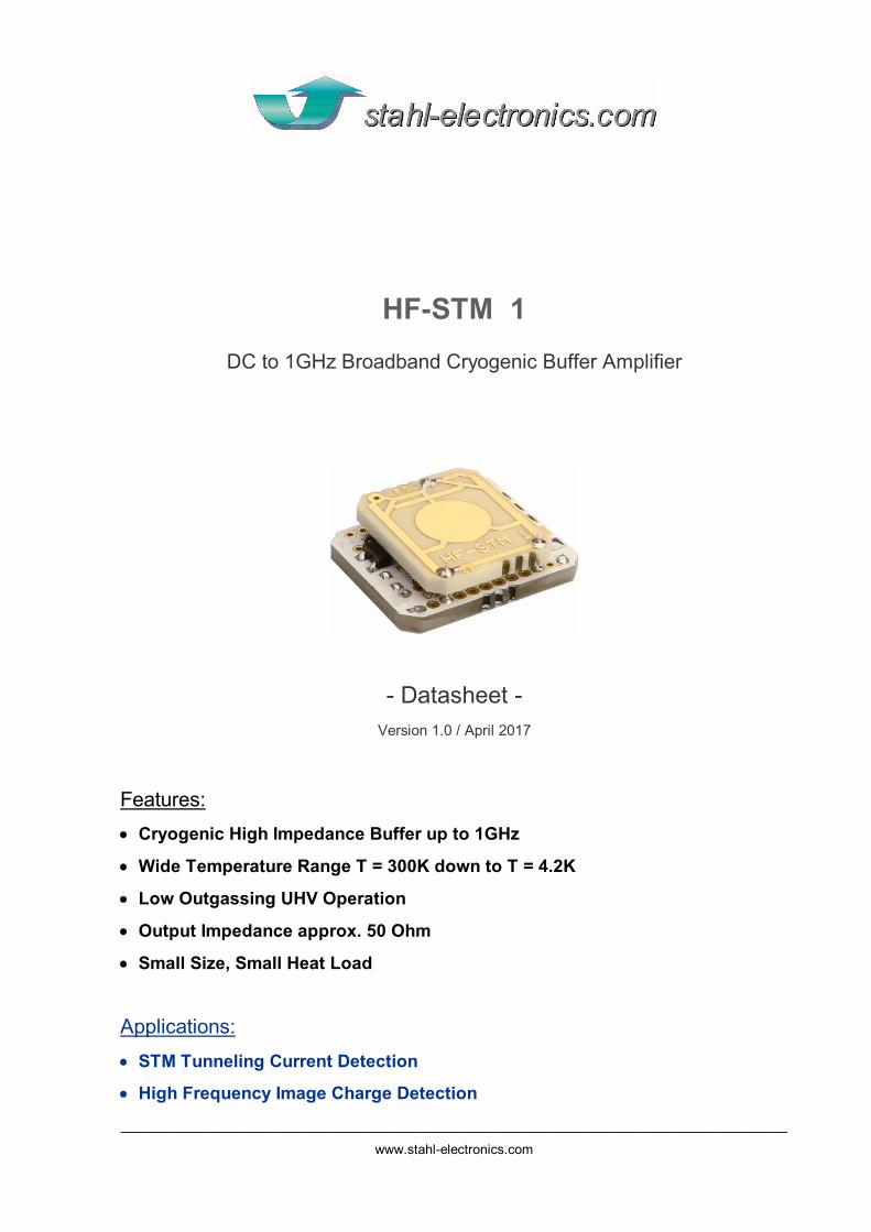
HF-STM 1
DC to 1GHz Broadband Cryogenic Buffer Amplifier
- Datasheet -
Version 1.0 / April 2017
Features:
Cryogenic High Impedance Buffer up to 1GHz
Wide Temperature Range T = 300K down to T = 4.2K
Low Outgassing UHV Operation
Output Impedance approx. 50 Ohm
Small Size, Small Heat Load
Applications:
STM Tunneling Current Detection
High Frequency Image Charge Detection
_________________________________________________________________________
www.stahl-electronics.com
Manual & Datasheet HF-STM 1, April 2017
2
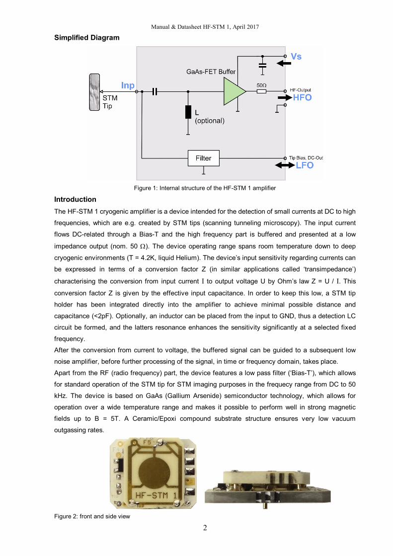
Simplified Diagram
Figure 1: Internal structure of the HF-STM 1 amplifier
Introduction
The HF-STM 1 cryogenic amplifier is a device intended for the detection of small currents at DC to high
frequencies, which are e.g. created by STM tips (scanning tunneling microscopy). The input current
flows DC-related through a Bias-T and the high frequency part is buffered and presented at a low
impedance output (nom. 50 ). The device operating range spans room temperature down to deep
cryogenic environments (T = 4.2K, liquid Helium). The device’s input sensitivity regarding currents can
be expressed in terms of a conversion factor Z (in similar applications called ‘transimpedance’)
characterising the conversion from input current I to output voltage U by Ohm’s law Z = U / I. This
conversion factor Z is given by the effective input capacitance. In order to keep this low, a STM tip
holder has been integrated directly into the amplifier to achieve minimal possible distance and
capacitance (<2pF). Optionally, an inductor can be placed from the input to GND, thus a detection LC
circuit be formed, and the latters resonance enhances the sensitivity significantly at a selected fixed
frequency.
After the conversion from current to voltage, the buffered signal can be guided to a subsequent low
noise amplifier, before further processing of the signal, in time or frequency domain, takes place.
Apart from the RF (radio frequency) part, the device features a low pass filter (‘Bias-T’), which allows
for standard operation of the STM tip for STM imaging purposes in the frequecy range from DC to 50
kHz. The device is based on GaAs (Gallium Arsenide) semiconductor technology, which allows for
operation over a wide temperature range and makes it possible to perform well in strong magnetic
fields up to B = 5T. A Ceramic/Epoxi compound substrate structure ensures very low vacuum
outgassing rates.
Figure 2: front and side view
Manual & Datasheet HF-STM 1, April 2017
3
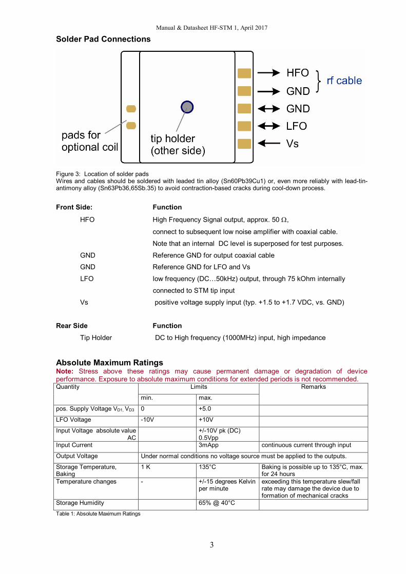
Solder Pad Connections
Figure 3: Location of solder padsWires and cables should be soldered with leaded tin alloy (Sn60Pb39Cu1) or, even more reliably with lead-tin-antimony alloy (Sn63Pb36,65Sb.35) to avoid contraction-based cracks during cool-down process.
Front Side: Function
HFO High Frequency Signal output, approx. 50 ,
connect to subsequent low noise amplifier with coaxial cable.
Note that an internal DC level is superposed for test purposes.
GND Reference GND for output coaxial cable
GND Reference GND for LFO and Vs
LFO low frequency (DC…50kHz) output, through 75 kOhm internally
connected to STM tip input
Vs positive voltage supply input (typ. +1.5 to +1.7 VDC, vs. GND)
Rear Side Function
Tip Holder DC to High frequency (1000MHz) input, high impedance
Absolute Maximum RatingsNote: Stress above these ratings may cause permanent damage or degradation of deviceperformance. Exposure to absolute maximum conditions for extended periods is not recommended.
LimitsQuantity
min. max.
Remarks
pos. Supply Voltage VD1, VD3 0 +5.0
LFO Voltage -10V +10V
Input Voltage absolute valueAC
+/-10V pk (DC)0.5Vpp
Input Current 3mApp continuous current through input
Output Voltage Under normal conditions no voltage source must be applied to the outputs.
Storage Temperature,Baking
1 K 135°C Baking is possible up to 135°C, max.for 24 hours
Temperature changes - +/-15 degrees Kelvinper minute
exceeding this temperature slew/fallrate may damage the device due toformation of mechanical cracks
Storage Humidity 65% @ 40°C
Table 1: Absolute Maximum Ratings
Manual & Datasheet HF-STM 1, April 2017
4
Characteristic Data and Operating Parameters
Parameter typical Value Remarks/Conditions
Freq. Rangehigh frequency buffer
.approx. 1MHz to 1GHz details see fig. 4
Voltage gain, T = 4 to 300K0.66 V/V ,0.31 V/V
corresponding to 9.4dBinsertion loss (50)
Biasing: Vs = 1.75V, f = 5MHzhigh impedance load,
50 output load
Output Impedancetyp. 50
Vs = 1.75V
Input Impedance vs. GNDDC: > 100M
AC: 1.85pF ±0.2pF// 70k
LFO left open (unbiased)DC to approx. 50kHz
Bias-TResistance between input and
LFO terminalFrequency range
75 k
DC to approx. 50kHz
The LFO terminal can be regarded asaccess to the DC path in a Bias-T
Useful Resonance Inductancerange in resonant mode 40nH … 10µH Note that coil should be 4K suited
AC Output Power< 7mW
Input Voltage Noise Densityf = 10 to 300MHz
Input Current Noise Density
0.4nV/Hz
approx. 150 fA/Hz @ 100MHz
@ T = 4.2K
@ T = 4.2K
Operating voltages
Vs, positive supply voltage +1.5 to +3.3 V T = 300K down to 4.2K1.75V recommended
Supply Currentsupply current Pin Vs 1.8 mA @1.5V =Vs
2.0 mA @1.75V =Vs T< 10KPower Consumption
2.7 to 3.5mW Supply 1.5V to 1.75VGeneral Operating Temperature
T = 4.2 K … 300 KExternal magnetic field
B = 0 … 5TGeometrical Size 18.1mm x 14.6mm x 6 mmOutgassing (to be determined)
Remark: This table represents typical values at low magnetic fields B < 1T. Parametersmay vary at higher B-fields.
Table 2: Characteristic Data
Caution: Electrostatic Sensitivity
Practical Hint:In case the device is picked up by hand, ensure that the ground pin or gold plated case istouched first before touching any other pin. Touching any other pin than ground first, maydestroy this device. Similar precaution has to be applied when changing the place of thedevice: Most important the destinations ground has to be on the same potential as thedevices ground. Therefore connect both grounds first before making any other connection orchanging the device position. Please follow also the commonly known ESD rules in literatureor internet.
This device can be damaged by ESD (Electrostatic Discharge), especially the inputand output lines. It is strongly recommended to handle the device with appropriateprecaution. Failure to observe proper handling and installation procedures can causeserious damage. This ESD damage can range from subtle performance degradation tocomplete device failure.
Manual & Datasheet HF-STM 1, April 2017
5
Voltage Supplies and Basic Operation
To bring the device into basic operation, a positive and stabilized supply voltage (connected to pin ‘Vs’)
is required (connect the current return path to one of the GND pads). The recommended value for Vs
equals 1.75V, even though it is not critical. Higher values (e.g. 3.3V) may slightly improve the signal to
noise ratio, but also increase the tendency for unwanted self-oscillations, depending on the geometry
surrounding the device and also inreases heat load. Any signal in the frequency range between 1MHz
and 1GHz appears as buffered voltage at the output. For further signal processing a terminated
(coaxial) cable should connect to subsequent signal processing stages.
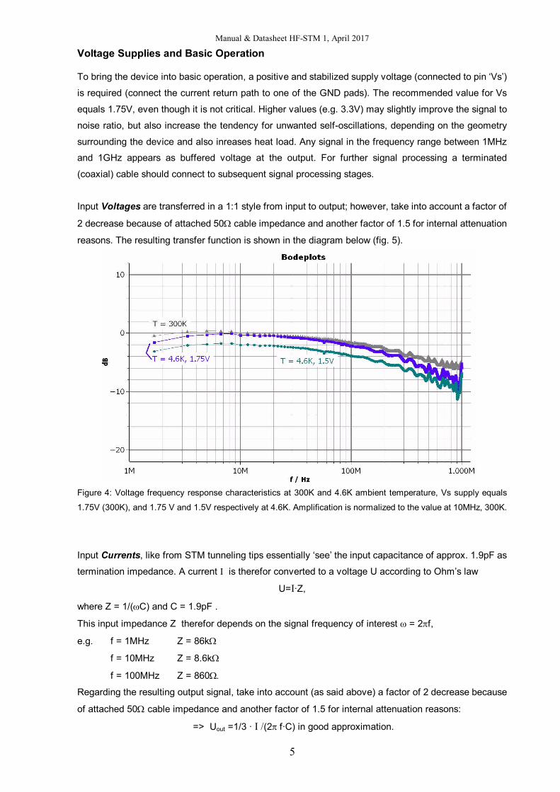
Input Voltages are transferred in a 1:1 style from input to output; however, take into account a factor of
2 decrease because of attached 50 cable impedance and another factor of 1.5 for internal attenuation
reasons. The resulting transfer function is shown in the diagram below (fig. 5).
Figure 4: Voltage frequency response characteristics at 300K and 4.6K ambient temperature, Vs supply equals
1.75V (300K), and 1.75 V and 1.5V respectively at 4.6K. Amplification is normalized to the value at 10MHz, 300K.
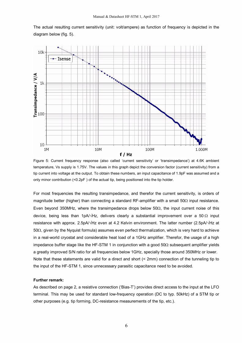
Input Currents, like from STM tunneling tips essentially ‘see’ the input capacitance of approx. 1.9pF as
termination impedance. A current I is therefor converted to a voltage U according to Ohm’s law
U=I·Z,
where Z = 1/(C) and C = 1.9pF .
This input impedance Z therefor depends on the signal frequency of interest = 2f,
e.g. f = 1MHz Z = 86k
f = 10MHz Z = 8.6k
f = 100MHz Z = 860
Regarding the resulting output signal, take into account (as said above) a factor of 2 decrease because
of attached 50 cable impedance and another factor of 1.5 for internal attenuation reasons:
=> Uout =1/3 · I /(2f·C) in good approximation.
Manual & Datasheet HF-STM 1, April 2017
6
The actual resulting current sensitivity (unit: volt/ampere) as function of frequency is depicted in the
diagram below (fig. 5).
Figure 5: Current frequency response (also called ‘current sensitivity’ or ‘transimpedance’) at 4.6K ambient
temperature, Vs supply is 1.75V. The values in this graph depict the conversion factor (current sensitivity) from a
tip current into voltage at the output. To obtain these numbers, an input capacitance of 1.9pF was assumed and a
only minor contribution (<0.2pF ) of the actual tip, being positioned into the tip holder.
For most frequencies the resulting transimpedance, and therefor the current sensitivity, is orders of
magnitude better (higher) than connecting a standard RF-amplifier with a small 50 input resistance.
Even beyond 350MHz, where the transimpedance drops below 50, the input current noise of this
device, being less than 1pA/√Hz, delivers clearly a substantial improvement over a 50 input
resistance with approx. 2.5pA/√Hz even at 4.2 Kelvin environment. The latter number (2.5pA/√Hz at
50, given by the Nyquist formula) assumes even perfect thermalization, which is very hard to achieve
in a real-world cryostat and considerable heat load of a 1GHz amplifier. Therefor, the usage of a high
impedance buffer stage like the HF-STM 1 in conjunction with a good 50 subsequent amplifier yields
a greatly improved S/N ratio for all frequencies below 1GHz, specially those around 350MHz or lower.
Note that these statements are valid for a direct and short (< 2mm) connection of the tunneling tip to
the input of the HF-STM 1, since unnecessary parasitic capacitance need to be avoided.
Further remark:
As described on page 2, a resistive connection (‘Bias-T’) provides direct access to the input at the LFO
terminal. This may be used for standard low-frequency operation (DC to typ. 50kHz) of a STM tip or
other purposes (e.g. tip forming, DC-resistance measurements of the tip, etc.).
Manual & Datasheet HF-STM 1, April 2017
7
Bias Filtering and Shielding
Grounding and Shielding at the input and output side are important issues of concern. A proper
grounding and shielding is essential to maintain good device performance and low noise
characteristics, and to avoid the creation of parasitic oscillations, which is a common problem to high-
frequency amplifiers with a high-impedance input. To ensure a “clean” electrical environment, provide
good ground connections especially around the amplifier input and STM tip. The signal output should
be connected through a coaxial line to the subsequent amplifier.
In case of self-oscillations, these uncontrollable oscillations appear typically at frequencies of about 50
to 500 MHz and are mostly an indication of insufficient shielding or grounding. In case this occurs, a
tight metal shield (Faraday cage), completely enclosing both signal source and amplifier input will
normally remove that problem. This shield should be connected to one of the ground pads of the
device.
For optimum noise performance the supply line (Vs) should be filtered well and be supplied from a well-
stabilized power supply. Standard blocking capacitors of 100nF from the biasing supply line to ground
may support power supply stabilization at the point of electrical feedthroughs leading into the vacuum
vessel.
HFO Cabling
The cabling from the RF output (‘HFO’-Pad) to the room temperature section (or subsequent amplifier)
requires special attention. A coaxial cable should be used with a well-defined characteristic impedance
along the whole distance between the cryo- and roomtemperature amplifier (or subsequent stage). This
is important since the signals of interest reside in a region in which an interrupted cable impedance
along the line distance can lead to severe signal reflections. The latter results in significant loss of
signal (S/N drops) and furthermore increases the risk of unwanted self-oscillations of the buffer
amplifier. A suitable cryo-compatible coaxial cable is for instance the GVLZ 081 (distributor: GVL
Cryoengeneering) or e.g. Lakeshore Type C cable. Note that despite the fact that the amplifiers output
has nominally 50 Ohm impedance, the attachement of a cable of different impedance (GVLZ 081: 75
Ohm) usually poses no problem as long as the cable end is well-terminated with an appropriate
termination resistor and therefore no (or only little) signal reflections are created. The occurrence of
unwanted self-oscillations of the device is an indication of a possible missing (or faulty) termination
resistor, cable interruption or discontinuity of impedance after the output connection. Note that the latter
(discontinuity of impedance) can normally not be detected with a standard multimeter, but with RF
(radio frequency) equipment.
Geometrically the coaxial cable should be connected in a direct and very close kind to the pins HFO
and GND, such that a defined (RF) impedance starts no more than 1mm away from the solder pads.
Manual & Datasheet HF-STM 1, April 2017
8
Thermal Anchoring
In a vacuum cryostat a good thermal coupling to the cold reservoir (cold finger, or Helium cryostat cold
plate) is required to ensure proper operation and low noise. Thermal connection should be established
using the round pad in the base plate of the amplifier, e.g. by pressing to a mating cooling plate or
permanent connection (soldering, glueing with conductive epoxi). Note that a thermally conducting
agent like “Apiezon N” grease between the metal pieces of different temperatures also greatly
increases the thermal heat flow.
Commissioning in a Vacuum or Cryogenic Setup
After wiring the device and mounting into a cryogenic dewar or vacuum chamber (always connect
ground lines first for ESD reasons), the device may be checked and eventually powered up with
appropriate supply voltages.
However, before power is applied to the device, one should carefully check the cable connections in
order to avoid damage or malfunction or cooling down in vain. With a standard multimeter (DMM) one
can perform a quick check of resistances. The following table lists typical values of connection lines
versus GND.
Line designator Resistance vs. GND Remark
Vs approx. 620 value differs in the order of 20% over 4K to 300K range
HFO 10.5 k value only slightly differs over 4K-300K range
LFO > 200 M input STM tip not mechanically connected to substrate yet
Table 3: typical resistance values versus GND, measured with a standard multimeter.
Cool-Down Procedure
Once mounted inside a cryostat setup, it is recommended to re-check the cabling (using a DMM in -
Mode, table above) as mentioned before. In case the latter is correct, one may power-up the device. A
typical consumption current of 2mA at room temperature will be drawn from Vs as positive supply
current. A DC-output voltage of approx. 50% of the supply voltage (applied to Vs) is measured on the
output line in case of proper operation.
During cool down in a cryostat or during the pumping process in a vacuum vessel one may from time to
time recheck the resistance of lines (as described above), or, once the device is powered up the DC
output value, since the latter represent an important check of the device functionality.
In general the device is operational over the complete range from 300K to 4.2K.
During cool-down/warm-up procedures always maintain a temperature rise or decrease of no more
than +/-15 degrees Kelvin per minute. Note that exceeding this temperature slew/fall rate may damage
the device due to formation of mechanical cracks. Never apply thermal shocks to the device, like
sudden dipping into a cryogenic liquid !
Manual & Datasheet HF-STM 1, April 2017
9
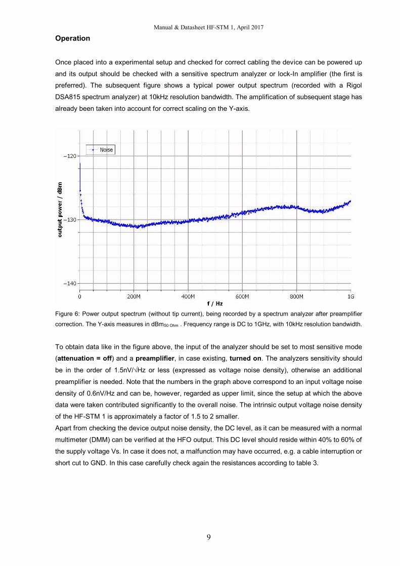
Operation
Once placed into a experimental setup and checked for correct cabling the device can be powered up
and its output should be checked with a sensitive spectrum analyzer or lock-In amplifier (the first is
preferred). The subsequent figure shows a typical power output spectrum (recorded with a Rigol
DSA815 spectrum analyzer) at 10kHz resolution bandwidth. The amplification of subsequent stage has
already been taken into account for correct scaling on the Y-axis.
Figure 6: Power output spectrum (without tip current), being recorded by a spectrum analyzer after preamplifier
correction. The Y-axis measures in dBm50 Ohm . Frequency range is DC to 1GHz, with 10kHz resolution bandwidth.
To obtain data like in the figure above, the input of the analyzer should be set to most sensitive mode
(attenuation = off) and a preamplifier, in case existing, turned on. The analyzers sensitivity should
be in the order of 1.5nV/√Hz or less (expressed as voltage noise density), otherwise an additional
preamplifier is needed. Note that the numbers in the graph above correspond to an input voltage noise
density of 0.6nV/Hz and can be, however, regarded as upper limit, since the setup at which the above
data were taken contributed significantly to the overall noise. The intrinsic output voltage noise density
of the HF-STM 1 is approximately a factor of 1.5 to 2 smaller.
Apart from checking the device output noise density, the DC level, as it can be measured with a normal
multimeter (DMM) can be verified at the HFO output. This DC level should reside within 40% to 60% of
the supply voltage Vs. In case it does not, a malfunction may have occurred, e.g. a cable interruption or
short cut to GND. In this case carefully check again the resistances according to table 3.
Manual & Datasheet HF-STM 1, April 2017
10
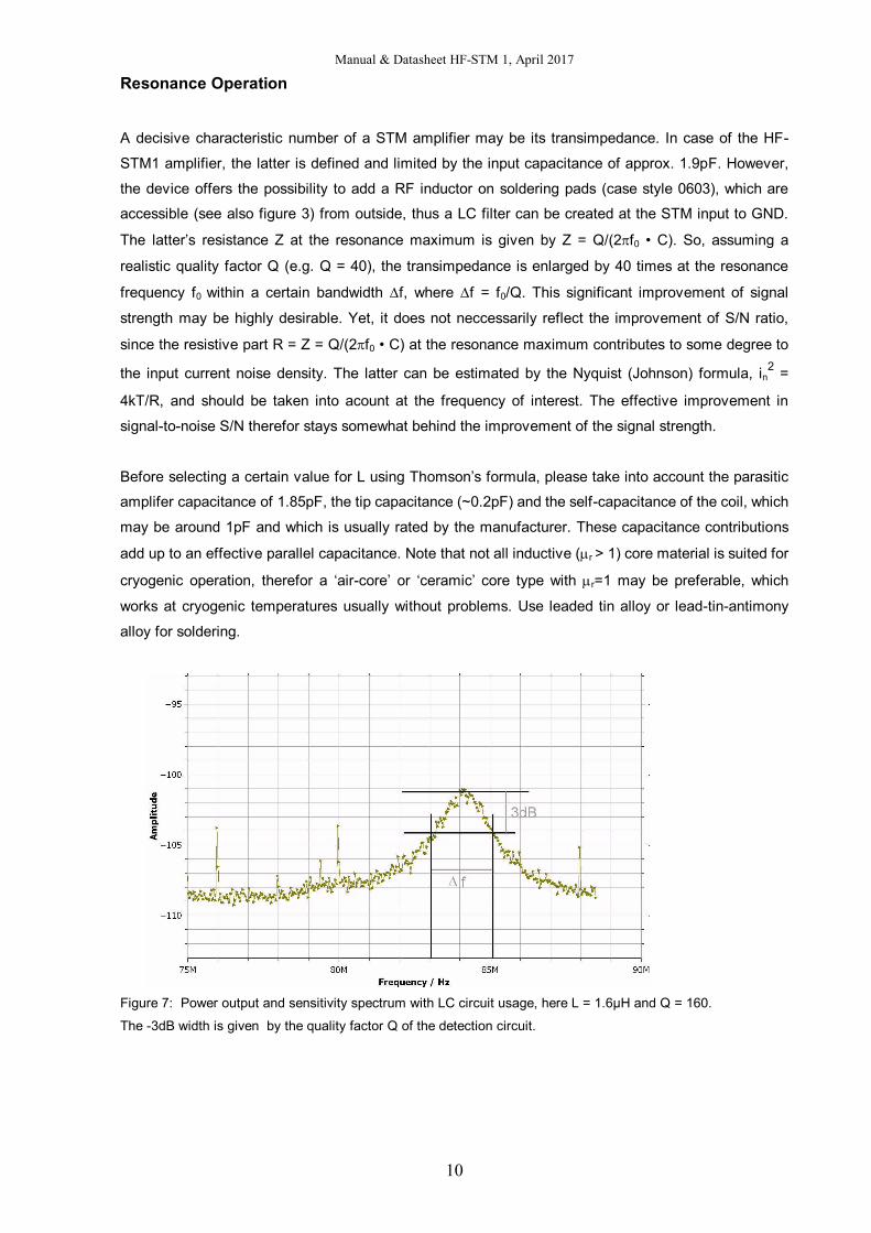
Resonance Operation
A decisive characteristic number of a STM amplifier may be its transimpedance. In case of the HF-
STM1 amplifier, the latter is defined and limited by the input capacitance of approx. 1.9pF. However,
the device offers the possibility to add a RF inductor on soldering pads (case style 0603), which are
accessible (see also figure 3) from outside, thus a LC filter can be created at the STM input to GND.
The latter’s resistance Z at the resonance maximum is given by Z = Q/(2f0 • C). So, assuming a
realistic quality factor Q (e.g. Q = 40), the transimpedance is enlarged by 40 times at the resonance
frequency f0 within a certain bandwidth f, where f = f0/Q. This significant improvement of signal
strength may be highly desirable. Yet, it does not neccessarily reflect the improvement of S/N ratio,
since the resistive part R = Z = Q/(2f0 • C) at the resonance maximum contributes to some degree to
the input current noise density. The latter can be estimated by the Nyquist (Johnson) formula, in2
=
4kT/R, and should be taken into acount at the frequency of interest. The effective improvement in
signal-to-noise S/N therefor stays somewhat behind the improvement of the signal strength.
Before selecting a certain value for L using Thomson’s formula, please take into account the parasitic
amplifer capacitance of 1.85pF, the tip capacitance (~0.2pF) and the self-capacitance of the coil, which
may be around 1pF and which is usually rated by the manufacturer. These capacitance contributions
add up to an effective parallel capacitance. Note that not all inductive (r > 1) core material is suited for
cryogenic operation, therefor a ‘air-core’ or ‘ceramic’ core type with r=1 may be preferable, which
works at cryogenic temperatures usually without problems. Use leaded tin alloy or lead-tin-antimony
alloy for soldering.
Figure 7: Power output and sensitivity spectrum with LC circuit usage, here L = 1.6µH and Q = 160.
The -3dB width is given by the quality factor Q of the detection circuit.
Manual & Datasheet HF-STM 1, April 2017
11
Appendix:
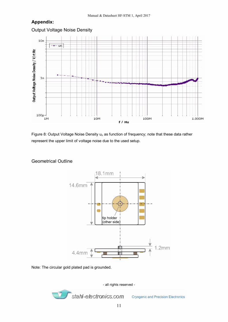
Output Voltage Noise Density
Figure 8: Output Voltage Noise Density un as function of frequency; note that these data rather
represent the upper limit of voltage noise due to the used setup.
Geometrical Outline
Note: The circular gold plated pad is grounded.
- all rights reserved -