helix single board computer - diamond systems user manual... · helix user manual revision a.02...
TRANSCRIPT

Helix User Manual Revision A.02 www.diamondsystems.com Page 1
Helix Single Board Computer PC/104 SBC with DMP Vortex86DX3 SoC
Copyright 2016 FOR TECHNICAL SUPPORT Diamond Systems Corporation PLEASE CONTACT: 158 Commercial Street Sunnyvale, CA 94086 USA [email protected] Tel 1-650-810-2500 Fax 1-650-810-2525 www.diamondsystems.com
Revision Date Comment
A.00 5/24/2016 Initial Release
A.01 6/16/2016 Data Acquisition section expanded
A.02 7/6/16 Additional information added
A.03 3/27/17 Boot Device Option note added
A.04 4/24/17 AC Adapter information updated
A.05 8/02/17 Quick Setup information updated

Helix User Manual Revision A.02 www.diamondsystems.com Page 2
CONTENTS
1. Important Safe Handling Information .............................................................................................................5 2. Introduction .......................................................................................................................................................7
2.1 Available Models............................................................................................................................................7 2.2 Features .........................................................................................................................................................7 2.3 Operating System Support ............................................................................................................................8 2.4 Mechanical, Electrical, Environmental ...........................................................................................................8 2.5 Customization Options ..................................................................................................................................8
3. Functional Block Diagram ...............................................................................................................................9 3.1 Feature Descriptions .................................................................................................................................. 10
3.1.1 Processor and Memory ...................................................................................................................... 10 3.1.2 Ethernet.............................................................................................................................................. 10 3.1.3 Video .................................................................................................................................................. 10 3.1.4 SATA .................................................................................................................................................. 10 3.1.5 USB .................................................................................................................................................... 10 3.1.6 PS/2 Keyboard and Mouse ................................................................................................................ 11 3.1.7 Serial Ports ........................................................................................................................................ 12 3.1.8 Audio .................................................................................................................................................. 12 3.1.9 Data Acquisition (DAQ) ...................................................................................................................... 12 3.1.10 Backup Battery ................................................................................................................................... 12 3.1.11 PCIe MiniCard / mSATA Socket ........................................................................................................ 12 3.1.12 PC/104 Expansion ............................................................................................................................. 12 3.1.13 PCIe Link Routing .............................................................................................................................. 12 3.1.14 Watchdog Timer ................................................................................................................................. 13 3.1.15 LED Indicators ................................................................................................................................... 14 3.1.16 BIOS Features ................................................................................................................................... 14 3.1.17 Power Supply ..................................................................................................................................... 15
4. Mechanical Board Drawing ........................................................................................................................... 16 5. Board Layout .................................................................................................................................................. 17
5.1 I/O Connectors, Jumpers and LED Summary ............................................................................................ 18 6. I/O Connectors ............................................................................................................................................... 19
6.1 Connector Pinout and Signal Description ................................................................................................... 19 6.1.1 PC/104 (J1, J2) .................................................................................................................................. 19 6.1.2 Audio (J3) ........................................................................................................................................... 20 6.1.3 USB 2.0 Ports (J4, J5, J6) ................................................................................................................. 20 6.1.4 Serial Ports (J7, J8) ........................................................................................................................... 20 6.1.5 LCD Backlight (J9) ............................................................................................................................. 21 6.1.6 Power In (J10) .................................................................................................................................... 21 6.1.7 External Battery (J11) ........................................................................................................................ 21 6.1.8 PS/2 Keyboard and Mouse (J12) ....................................................................................................... 22 6.1.9 VGA (J13) .......................................................................................................................................... 22 6.1.10 Ethernet (J14, J15) ............................................................................................................................ 22 6.1.11 Utility (J16) ......................................................................................................................................... 23 6.1.12 Digital I/O (J17) .................................................................................................................................. 23 6.1.13 Analog I/O (J18) ................................................................................................................................. 24 6.1.14 SATA (J19) ........................................................................................................................................ 25 6.1.15 CAN (J20) .......................................................................................................................................... 25 6.1.16 LVDS LCD (J21) ................................................................................................................................ 25 6.1.17 PCIe MiniCard / mSATA Socket (J24) ............................................................................................... 26
6.2 List Of Connectors ...................................................................................................................................... 27 7. I/O CableS ....................................................................................................................................................... 28 8. Jumper Description ....................................................................................................................................... 29
8.1 Digital IO (JP1) ........................................................................................................................................... 30 8.2 CAN Termination (JP2) .............................................................................................................................. 30 8.3 Miscellaneous (JP3) ................................................................................................................................... 31 8.4 RS-422/485 Termination (JP4) ................................................................................................................... 32 8.5 LVDS Backlight and LVDS VDD (JP5) ....................................................................................................... 33 8.6 IRQ Selection (JP6) .................................................................................................................................... 33
9. BIOS Key Features......................................................................................................................................... 34 9.1 Entering the BIOS ....................................................................................................................................... 34 9.2 Restoring Default BIOS Settings ................................................................................................................ 34

Helix User Manual Revision A.02 www.diamondsystems.com Page 3
9.3 Upgrading BIOS using DOS Utility ............................................................................................................. 34 9.4 Setting the Date and Time .......................................................................................................................... 34 9.5 Boot Priority ................................................................................................................................................ 34 9.6 LED ............................................................................................................................................................. 35 9.7 Watchdog Timer ......................................................................................................................................... 35 9.8 Quiet / Quick Boot / Splash Screen ............................................................................................................ 35 9.9 Serial Port Configuration ............................................................................................................................ 35
10. Getting Started ............................................................................................................................................... 36 10.1 Development Kit Contents .......................................................................................................................... 36 10.2 Quick Setup ................................................................................................................................................ 36 10.3 Boot Device Options ................................................................................................................................... 36 10.4 Installing OS and Booting ........................................................................................................................... 37
11. Video Features ............................................................................................................................................... 38 11.1 VGA ............................................................................................................................................................ 38 11.2 LCD ............................................................................................................................................................. 38
11.2.1 Backlight............................................................................................................................................. 38 11.3 Dual Display ................................................................................................................................................ 38 11.4 Changing LCD Resolution .......................................................................................................................... 39
11.4.1 Step 1: Modify the VBIOS file ............................................................................................................ 39 11.4.2 Step 2: Integrate the VBIOS with the BIOS file ................................................................................. 41
12. Serial Ports and System Console ................................................................................................................ 43 12.1 Overview ..................................................................................................................................................... 43 12.2 Configuration .............................................................................................................................................. 43 12.3 Console redirection ..................................................................................................................................... 43
13. MASS STORAGE ............................................................................................................................................ 44 13.1 Flashdisk Models and Capacities ............................................................................................................... 44 13.2 Installation and Configuration ..................................................................................................................... 44
14. Utility Connector Features ............................................................................................................................ 45 14.1 I2C .............................................................................................................................................................. 45 14.2 Reset .......................................................................................................................................................... 45 14.3 Gigabit Ethernet LED Signals ..................................................................................................................... 45 14.4 Power and Ground ..................................................................................................................................... 45
15. A Model Data Acquisition Circuit ................................................................................................................. 46 15.1 Features ...................................................................................................................................................... 46 15.2 Block Diagram ............................................................................................................................................ 47 15.3 Analog-to-Digital Circuit .............................................................................................................................. 47
15.3.1 A/D Circuit Overview .......................................................................................................................... 47 15.3.2 A/D Channel Selection, Sampling, and Timing .................................................................................. 48 15.3.3 A/D FIFO and High Speed Sampling ................................................................................................. 48 15.3.4 A/D Operation .................................................................................................................................... 49 15.3.5 A/D Resolution ................................................................................................................................... 49 15.3.6 Input Range Selection ........................................................................................................................ 50 15.3.7 Converting A/D Readings to Volts or Engineering Units ................................................................... 50 15.3.8 Measurement Accuracy and Calibration ............................................................................................ 51 15.3.9 Input Impedance ................................................................................................................................ 51
15.4 Digital-to-Analog Circuit .............................................................................................................................. 52 15.4.1 Overview ............................................................................................................................................ 52 15.4.2 D/A Resolution ................................................................................................................................... 52 15.4.3 Output Range Selection ..................................................................................................................... 52 15.4.4 D/A Conversion Formula .................................................................................................................... 53 15.4.5 Output Accuracy and Calibration ....................................................................................................... 53
15.5 Digital I/O Features ..................................................................................................................................... 54 15.5.1 Overview ............................................................................................................................................ 54 15.5.2 Edge Detection Circuit ....................................................................................................................... 54 15.5.3 Support for Special Functions ............................................................................................................ 55 15.5.4 Power Pins ......................................................................................................................................... 55
15.6 Counter/Timer Features ............................................................................................................................. 55 15.6.1 Overview ............................................................................................................................................ 55 15.6.2 Counter Commands ........................................................................................................................... 56 15.6.3 Counter I/O Signals ............................................................................................................................ 56 15.6.4 Counter Advanced Features .............................................................................................................. 56
15.7 Pulse Width Modulator Features ................................................................................................................ 57

Helix User Manual Revision A.02 www.diamondsystems.com Page 4
15.7.1 Overview ............................................................................................................................................ 57 15.7.2 PWM Commands ............................................................................................................................... 57 15.7.3 PWM Output Signals .......................................................................................................................... 57
15.8 Interrupt Operation ..................................................................................................................................... 58 15.8.1 Overview ............................................................................................................................................ 58 15.8.2 Interrupt Sources ............................................................................................................................... 58
16. “D” Model Digital I/O Circuit ......................................................................................................................... 59 16.1 Features ...................................................................................................................................................... 59 16.2 Block Diagram ............................................................................................................................................ 59 16.3 Configuration and Programming................................................................................................................. 60
16.3.1 Register Map ...................................................................................................................................... 60 16.3.2 Programming Instructions .................................................................................................................. 61
17. PC/104 I/O Expansion .................................................................................................................................... 61 17.1 Address Ranges Available ......................................................................................................................... 61 17.2 IRQs Available ............................................................................................................................................ 61
18. Software Driver Overview ............................................................................................................................. 62 19. Specifications ................................................................................................................................................. 63

Helix User Manual Revision A.02 www.diamondsystems.com Page 5
1. IMPORTANT SAFE HANDLING INFORMATION
WARNING!
ESD-Sensitive Electronic Equipment
Observe ESD-safe handling procedures when working with this product.
Always use this product in a properly grounded work area and wear appropriate ESD-preventive clothing and/or accessories.
Always store this product in ESD-protective packaging when not in use.
Safe Handling Precautions
The Helix SBC contains a high number of I/O connectors with connection to sensitive electronic components. This creates many opportunities for accidental damage during handling, installation and connection to other equipment. The list here describes common causes of failure found on boards returned to Diamond Systems for repair. This information is provided as a source of advice to help you prevent damaging your Diamond (or any vendor’s) embedded computer boards.
ESD damage – This type of damage is usually almost impossible to detect, because there is no visual sign of failure or damage. The symptom is that the board eventually simply stops working, because some component becomes defective. Usually the failure can be identified and the chip can be replaced.
To prevent ESD damage, always follow proper ESD-prevention practices when handling computer boards.
Damage during handling or storage – On some boards we have noticed physical damage from mishandling. A common observation is that a screwdriver slipped while installing the board, causing a gouge in the PCB surface and cutting signal traces or damaging components.
Another common observation is damaged board corners, indicating the board was dropped. This may or may not cause damage to the circuitry, depending on what is near the corner. Most of our boards are designed with at least 25 mils clearance between the board edge and any component pad, and ground / power planes are at least 20 mils from the edge to avoid possible shorting from this type of damage. However these design rules are not sufficient to prevent damage in all situations.
A third cause of failure is when a metal screwdriver tip slips, or a screw drops onto the board while it is powered on, causing a short between a power pin and a signal pin on a component. This can cause overvoltage / power supply problems described below. To avoid this type of failure, only perform assembly operations when the system is powered off.
Sometimes boards are stored in racks with slots that grip the edge of the board. This is a common practice for board manufacturers. However our boards are generally very dense, and if the board has components very close to the board edge, they can be damaged or even knocked off the board when the board tilts back in the rack. Diamond recommends that all our boards be stored only in individual ESD-safe packaging. If multiple boards are stored together, they should be contained in bins with dividers between boards. Do not pile boards on top of each other or cram too many boards into a small location. This can cause damage to connector pins or fragile components.
Power supply wired backwards – Our power supplies and boards are not designed to withstand a reverse power supply connection. This will destroy each IC that is connected to the power supply (i.e. almost all ICs). In this case the board will most likely will be unrepairable and must be replaced. A chip destroyed by reverse power or by excessive power will often have a visible hole on the top or show some deformation on the top surface due to vaporization inside the package. Check twice before applying power!
Board not installed properly in PC/104 stack – A common error is to install a PC/104 board accidentally shifted by 1 row or 1 column. If the board is installed incorrectly, it is possible for power and ground signals on the bus to make contact with the wrong pins on the board, which can damage the board. For example, this can damage
components attached to the data bus, because it puts the 12V power supply lines directly on data bus lines.

Helix User Manual Revision A.02 www.diamondsystems.com Page 6
Overvoltage on analog input – If a voltage applied to an analog input exceeds the design specification of the board, the input multiplexor and/or parts behind it can be damaged. Most of our boards will withstand an
erroneous connection of up to 35V on the analog inputs, even when the board is powered off, but not all boards, and not in all conditions.
Overvoltage on analog output – If an analog output is accidentally connected to another output signal or a power supply voltage, the output can be damaged. On most of our boards, a short circuit to ground on an analog output will not cause trouble.
Overvoltage on digital I/O line – If a digital I/O signal is connected to a voltage above the maximum specified voltage, the digital circuitry can be damaged. On most of our boards the acceptable range of voltages connected to digital I/O signals is 0-5V, and they can withstand about 0.5V beyond that (-0.5 to 5.5V) before being damaged. However logic signals at 12V and even 24V are common, and if one of these is connected to a 5V logic chip, the chip will be damaged, and the damage could even extend past that chip to others in the circuit.
Bent connector pins – This type of problem is often only a cosmetic issue and is easily fixed by bending the pins back to their proper shape one at a time with needle-nose pliers. The most common cause of bent connector pins is when a PC/104 board is pulled off the stack by rocking it back and forth left to right, from one end of the connector to the other. As the board is rocked back and forth it pulls out suddenly, and the pins at the end get bent significantly. The same situation can occur when pulling a ribbon cable off of a pin header. If the pins are bent too severely, bending them back can cause them to weaken unacceptably or even break, and the connector must be replaced.

Helix User Manual Revision A.02 www.diamondsystems.com Page 7
2. INTRODUCTION
Helix is a compact, rugged single board computer that features the DMP Vortex86DX3 System on Chip (SoC) processor in an extended PC/104 form factor. The full rectangular shape provides more coastline for I/O connectors than other boards of its size. In this compact form factor, Helix includes a wide range of I/O plus data acquisition functionality, meeting the majority of today’s connectivity requirements in a single board.
2.1 Available Models
Model
Processor/ Speed
Memory
Analog I/O
Digital I/O
10/100 Ethernet
Port
Gigabit Ethernet
Port
USB2.0
HLX1000-2GA 1GHz 2GB Yes 27 1 1 6
HLX1000-1GD 1GHz 1GB No 16 1 1 3
HLX1000-2GD * 1GHz 2GB No 16 1 1 3
* Custom version, minimum order quantities apply
2.2 Features
1GHz DMP Vortex86DX3 dual core CPU
Up to 2GB DDR3 SDRAM soldered on board
I/O Support:
- 3 or 6 USB2.0 ports (model dependent)
- 2 RS-232/422/485 & 2 RS-232 ports
- 1 10/100Mbps Ethernet port
- 1 Gigabit Ethernet port
- 1 SATA port for disk-on-module or external drive
- 24-bit dual channel LVDS LCD display
- VGA CRT
- HD audio
- PCIe MiniCard socket shared with mSATA
- 16 digital I/O lines with programmable direction
Data Acquisition:
- 16 16-bit analog inputs
- 100KHz max sample rate
- 4 16-bit analog outputs
- 11 additional digital I/O lines with programmable direction
- 8 32-bit counter/timers
- 4 24-bit pulse width modulators
PC/104 stackable I/O expansion capability

Helix User Manual Revision A.02 www.diamondsystems.com Page 8
2.3 Operating System Support
Linux, Windows Embedded Standard 7
Both Linux and Windows Embedded 7 Software Development Kits are available with bootable images and drivers
2.4 Mechanical, Electrical, Environmental
PC/104 extended form factor (4.0” x 4.0”)
Extremely rugged with soldered RAM and -40°C to +85°C (-40°F to +185°F) operating temperature
Power input: +5VDC +/- 5% or optional +9 to 36VDC
2.5 Customization Options
The following customization options are available for the Helix single board computer. Minimum order quantities may apply for customization. Contact Diamond Systems sales or support for further information
2GB on-board DDR3 RAM instead of 1GB
1 CANbus 2.0 port
+9 to +36V 50W DC/DC wide voltage power input
Latching connectors instead of pin headers
Extended life backup battery
Replace configuration jumpers with 0 ohm resistors
Low profile heatsink
Conformal coating
Custom BIOS
Custom FPGA code

Helix User Manual Revision A.02 www.diamondsystems.com Page 9
3. FUNCTIONAL BLOCK DIAGRAM
Figure 1: Functional Block Diagram

Helix User Manual Revision A.02 www.diamondsystems.com Page 10
3.1 Feature Descriptions
This section describes the key subsystems of the Helix SBC.
3.1.1 Processor and Memory
Helix SBCs use the Vortex86DX3 SoC from DMP Electronics. It is a 32-bit x86 architecture dual-core 1GHz microprocessor designed for ultra-low power consumption, combining both the North and South bridges with a rich set of integrated features including a 32KB write through 8-way L1 cache, 512KB write through/write back 4-way L2 cache, PCIe bus at 2.5 GHz, DDR3 controller, ISA, I2C, SPI, IPC (includes Internal Peripheral Controllers with DMA and interrupt timer/counter), Fast Ethernet, FIFO UART, USB2.0 Host, and an IDE/SATA controller.
The SBC supports up to 2GB of DDR3 memory soldered on-board.
3.1.2 Ethernet
The Helix SBC provides two Ethernet ports. One is a 10/100 Ethernet port provisioned directly from the Vortex SoC (System on Chip). The second is a 10/100/1000 Ethernet port realized using an Intel I210IT PCIe Gigabit Ethernet Controller (MAC + PHY). The board also includes the necessary magnetics. Ethernet connections are via a pin header.
On-board LEDs are provided for Link, Activity, and Speed. The LEDs are located along the board edge near the Ethernet connector. The connector does not provide access to the LED signals.
3.1.3 Video
The SBC offers two display outputs: one VGA and one LVDS. The VGA interface comes directly from the processor and is made available on a 2x5 header. The LVDS interface is realized from the 24-bit DVO of the processor using a DS90C187LF chip.
The maximum display resolution is 1920 x 1080 at 60Hz. The SBC supports dual display mode. In dual display mode, the maximum resolution supported is 1280 x 1024 at 60Hz.
The LCD backlight control is provided by a PWM circuit. LCD backlight power and control signals are terminated on a separate latching connector.
3.1.4 SATA
The Helix SBC has one industry-standard vertical SATA connector that accepts cables with latching connectors. The SATA port is derived directly from the processor. It is connected to a connector placed on the board in a position that allows a miniature SATA disk-on-module (DOM) to be installed in it and attached with a mounting spacer and screw.
The board offers an additional SATA port derived from a x1 PCIe lane. This SATA port is available over the shared mSATA / PCIe MiniCard socket.
3.1.5 USB
The board provides seven user accessible USB 2.0 ports. Three of these comes directly from the processor, and are available on a 2x5 header.
The fourth port from the processor is connected to a 4-port USB hub from SMSC (USB2514). Three of the four downstream ports from the USB hub are connected to a 2x5 header and the fourth port is connected to the PCIe MiniCard socket. The USB configurations possible are depicted in the following images. The Helix A model offers all six USB ports. The D model offers only the three driven directly from the SoC.

Helix User Manual Revision A.02 www.diamondsystems.com Page 11
Option 1 : Six USB2.0 ports available on USB2.0 header (Helix A model)
Option 2: Three USB2.0 ports available on USB2.0 header (Helix D model)
3.1.6 PS/2 Keyboard and Mouse
Helix supports PS/2 keyboard and mouse driven directly from the Vortex SoC.

Helix User Manual Revision A.02 www.diamondsystems.com Page 12
3.1.7 Serial Ports
The SBC provides four serial ports: two with fixed RS-232 capability using SP211EHEA-L, and a second two having RS-232/422/485 capability using a SP336. The built-in UARTs from the VortexDX3 are used. In RS-232 mode, only the signals TX, RX, RTS, and CTS are provided. Protocol selection for serial ports 3-4 is controlled using GPIO pins from the SoC and is configurable via BIOS configuration screens as well as via application software. Jumpers are used to enable termination resistors (121 Ohm) for RS-422 and RS-485 protocols.
Console redirection, using a serial port for keyboard input and terminal display via a link to a second computer, is provided via the BIOS on serial port 1.
3.1.8 Audio
The SBC supports HD audio with an ALC892. Audio I/O signals include stereo line in, stereo line out and mic in.
3.1.9 Data Acquisition (DAQ)
The SBC provides an optional data acquisition circuit containing analog input, analog output, and additional digital I/O features. This circuit is controlled by an FPGA interfaced to the processor via SPI.
The data acquisition features include 16 single-ended / 8 differential analog inputs with 16-bit resolution, programmable input ranges, and a 100KHz maximum sample rate; 4 analog outputs with 16-bit resolution and programmable output ranges; and 11 additional digital I/O lines with selectable 3.3V logic levels, selectable pull-up/down resistors, programmable direction, buffered I/O, and capability for use as counter/timer and PWM circuits.
In models with DAQ support (A models), 27 total digital I/O lines are available on the DAQ Digital I/O and Analog I/O connectors. In models without DAQ (D models), 16 digital I/O lines from the VortexDX3 are made available on the Digital I/O connector.
3.1.10 Backup Battery
The SBC contains an on-board RTC backup battery. On models with fixed +5VDC input, a battery is mounted on the top side of the board. On custom models with wide voltage input, an extended life RTC battery is mounted on the bottom side of the board.
On all models, a connector is provided to enable the use of an external battery.
The SBC can boot and function properly without a backup battery installed. A jumper is provided to disconnect the battery during long term storage.
3.1.11 PCIe MiniCard / mSATA Socket
The Helix SBC has one full size (51mm length) shared PCIe MiniCard and mSATA socket. The socket supports both PCIe MiniCard and mSATA modules, one module at a time. It has a PCIe/mSATA switch controlled by a pin on the socket to select which interface is active.
A PCIe x1 lane is available on this connector directly from the Vortex86DX3 SoC. A USB port from the USB hub (SMSC USB2514) is also connected to the socket.
The SATA lane is realized from the same PCIex1 lane that connects to the PCIe MiniCard connector. A PCIe to SATA bridge chip ASM1061 is used as well as a mux to avoid stub on PCIe and SATA signals.
3.1.12 PC/104 Expansion
Helix provides stackable I/O expansion options over the PC/104 ISA bus. The ISA bus comes directly from the Vortex86DX3 SoC and supports DMA access. Refer to Section18 for details on the ISA addresses and IRQs available for the Windows 7 operating system.
3.1.13 PCIe Link Routing
Two PCIe lanes from the SoC are used to provide Gigabit Ethernet functionality and expansion card options. The lane configurations are as listed below.
Lane 1 (from SoC): Gigabit Ethernet
Lane 2 (from SoC): PCIe MiniCard / PCIe to SATA bridge

Helix User Manual Revision A.02 www.diamondsystems.com Page 13
3.1.14 Watchdog Timer
The Helix SBC has one watchdog timer (WDT) generated from the Vortex86DX3 SOC, WDT1. The WDT can be enabled/ disabled from BIOS or software. The timer can be triggered only from software. If the watchdog timer times out before it is retriggered, it will cause a system reset. The watchdog timer uses a 32.768KHz clock to count a 24-bit register. The timeout period is programmable from 30.5us to 512 seconds with a resolution of 30.5us.
Following are the registers associated with the watchdog timer, WDT1.
IO port Address (Hex) Register
A8 Watchdog Timer 1 control register
AA Watchdog Timer 1 Counter 0 register
AB Watchdog Timer 1 Counter 1 register
AC Watchdog Timer 1 Counter 2 register
AD Watchdog Timer 1 Status register
AE Watchdog Timer 1 Reload register
Watchdog Timer 1 Control Register (A8h)
Bit Name Attribute Description
7 RSVD - Reserved
6 WE RW WDT1 Enable control (Write bit = 1 to reload the WDT1 counter)
0: WDT1 disabled (default)
1: WDT1 enabled
5-0 RSVD - Reserved
Watchdog Timer 1 Counter Registers (AAh - ACh)
Bit Name Attribute Description
7-0 CNT0 RW Watchdog Timer 1 Counter 0 (Resolution is 30.5us)
15-8 CNT1 RW Watchdog Timer 1 Counter 1 (Resolution is 30.5us)
23-16 CNT2 RW Watchdog Timer 1 Counter 2 (Resolution is 30.5us)
Watchdog Timer 1 Status Register (ADh)
Bit Name Attribute Description
7 WDTF RW Watchdog timer 1Flag
0: WDT1 has not timed out
1: WDT1 has timed out. Write 1 to clear this flag. Writing 0 will have no effect.
6-0 RSVD - Reserved

Helix User Manual Revision A.02 www.diamondsystems.com Page 14
Watchdog Timer 1 Reload Register (AEh)
Bit Name Attribute Description
7-0 WDTRL W Write this register to reload WDT1 internal counter
Follow the below steps to setup the Watchdog timer:
1. Set Bit 6 (WE) of register A8h = 0 to disable the watchdog timer
2. Write the desired counter value (30.5us to 512 sec) to registers AAh-ACh
3. Set Bit 6 (WE) of register A8h = 1 to enable the watchdog timer
4. As the counter reaches the set value, system will reset
5. Any write to Reload register (AEh) before the counter times out will restart the counter
3.1.15 LED Indicators
The SBC provides the following LED indicators. All LEDs are located near a board edge or their respective features. The blue LED is located along the lower edge of the board. All LEDs are labeled in silkscreen with their function.
Power input: Green LED when input power is applied
Power on: Green LED when board is powered on
BIOS LED: Green LED connected to a GPIO line on the processor. This LED is off during power-up and is turned on by the BIOS to indicate a successful system BIOS startup.
Ethernet 10/100: Green LED for duplex and speed
GBE: Green LED for link, speed and activity
DAQ: Blue LED driven with reverse logic from +5V and controlled by the FPGA
DONE: Green LED driven by the FPGA. The LED comes on once the FPGA code is downloaded successfully
PCIe MiniCard socket: 3 Green LEDs to support WWAN, WPAN, WLAN signals from the connector
3.1.16 BIOS Features
In addition to supporting all the interfaces specified in the block diagram, the BIOS provides the following key features:
Boot from LAN (PXE only on 10/100 port) as well as USB and SATA ports
Free boot sequence configuration to allow different boot sequences as first, second and third boot devices
Support dual display mode, VGA and LVDS can be active simultaneously
Support for various LCD configurations
LCD backlight control using PWM; LCD VDD Enable using GPIO
Console redirection to one or more COM ports
ISA_IRQ 5 or ISA_IRQ_7 can be reserved for FPGA
Quiet boot option
POST message displays “Diamond Systems Corporation” and also displays the board name and BIOS version
FPGA ID readback in BIOS menu
Enable/disable for individual COM ports
Protocol selection for COM ports 3 and 4, default for all ports is RS-232
Enable/ disable digital I/O ports A and B (GPIO_P0 and GPIO_P1) from SoC
Direction control (Input/ Output) for digital I/O ports A and B
Ethernet MAC address read back on boot-up and in BIOS screens

Helix User Manual Revision A.02 www.diamondsystems.com Page 15
Single BIOS to support both 1GB and 2GB DDR3 memory configurations
BIOS LED to indicate successful BIOS initialization
Supports standard BIOS hotkey including DEL key to enter BIOS menu and END key to load BIOS default settings
Password protection
Field upgradeable via a DOS utility
WDT can be configured from BIOS setup menu -- timeout and action are screen-configurable and programmable
3.1.17 Power Supply
The Helix SBC is powered from a +5VDC input. As an optional custom feature, a 50W DC/DC wide voltage input circuit of +9V to +36V is also available.
All required supply voltages other than +12V are derived from the input supply. The power supplies are able to support the highest capacity on-board memory plus have enough reserve capacity to support the following add-on features:
5V 3.3V Feature
2.0A PC/104 add-on modules
1.5A PCIe MiniCard add-on modules
0.25A SATA disk module
1.4A 0.7A LCD power
0.9A LCD backlight
0.05A DAQ connector
0.05A Utility connector
3A USB 2.0 ports

Helix User Manual Revision A.02 www.diamondsystems.com Page 16
4. MECHANICAL BOARD DRAWING
Figure 2: Mechanical Board Drawing

Helix User Manual Revision A.02 www.diamondsystems.com Page 17
5. BOARD LAYOUT
Figure 3: Board Layout
J2
J1
LED Block 1
LED Block 2
LED Block 3
LED Block 4 J19
J3
J4
J5
J6
J7
JP4
J8
J9 JP5 J10 J11
J12
J13
J14
J15
J16
J18
JP3
J17
J20 J21 J24 J22 JP1 JP2
JP6
J25
Helix User Manual Revision A.02 www.diamondsystems.com Page 18
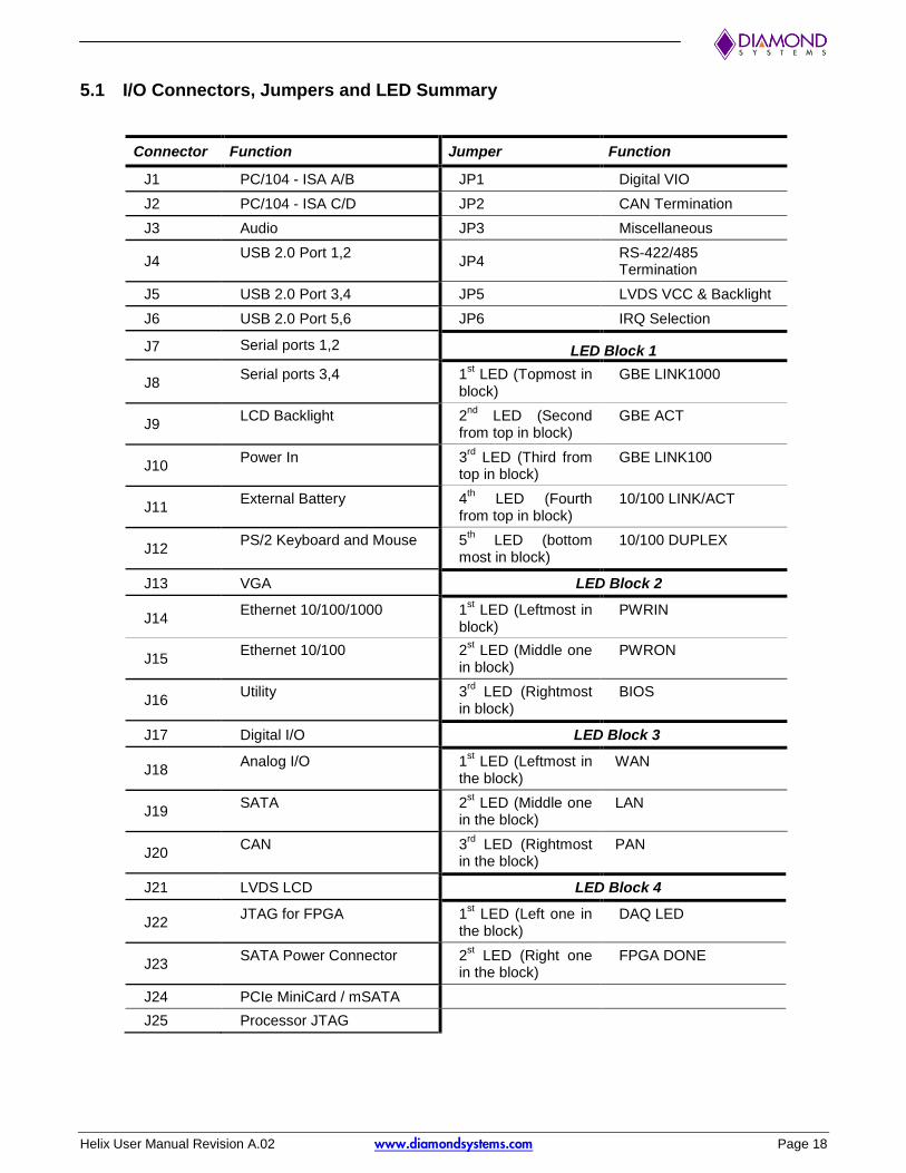
5.1 I/O Connectors, Jumpers and LED Summary
Connector Function Jumper Function
J1 PC/104 - ISA A/B JP1 Digital VIO
J2 PC/104 - ISA C/D JP2 CAN Termination
J3 Audio JP3 Miscellaneous
J4 USB 2.0 Port 1,2
JP4 RS-422/485 Termination
J5 USB 2.0 Port 3,4 JP5 LVDS VCC & Backlight
J6 USB 2.0 Port 5,6 JP6 IRQ Selection
J7 Serial ports 1,2 LED Block 1
J8 Serial ports 3,4 1
st LED (Topmost in
block) GBE LINK1000
J9 LCD Backlight 2
nd LED (Second
from top in block) GBE ACT
J10 Power In 3
rd LED (Third from
top in block) GBE LINK100
J11 External Battery 4
th LED (Fourth
from top in block) 10/100 LINK/ACT
J12 PS/2 Keyboard and Mouse 5
th LED (bottom
most in block) 10/100 DUPLEX
J13 VGA LED Block 2
J14 Ethernet 10/100/1000 1
st LED (Leftmost in
block) PWRIN
J15 Ethernet 10/100 2
st LED (Middle one
in block) PWRON
J16 Utility 3
rd LED (Rightmost
in block) BIOS
J17 Digital I/O LED Block 3
J18 Analog I/O 1
st LED (Leftmost in
the block) WAN
J19 SATA 2
st LED (Middle one
in the block) LAN
J20 CAN 3
rd LED (Rightmost
in the block) PAN
J21 LVDS LCD LED Block 4
J22 JTAG for FPGA 1
st LED (Left one in
the block) DAQ LED
J23 SATA Power Connector 2
st LED (Right one
in the block) FPGA DONE
J24 PCIe MiniCard / mSATA
J25 Processor JTAG
Helix User Manual Revision A.02 www.diamondsystems.com Page 19
6. I/O CONNECTORS
6.1 Connector Pinout and Signal Description
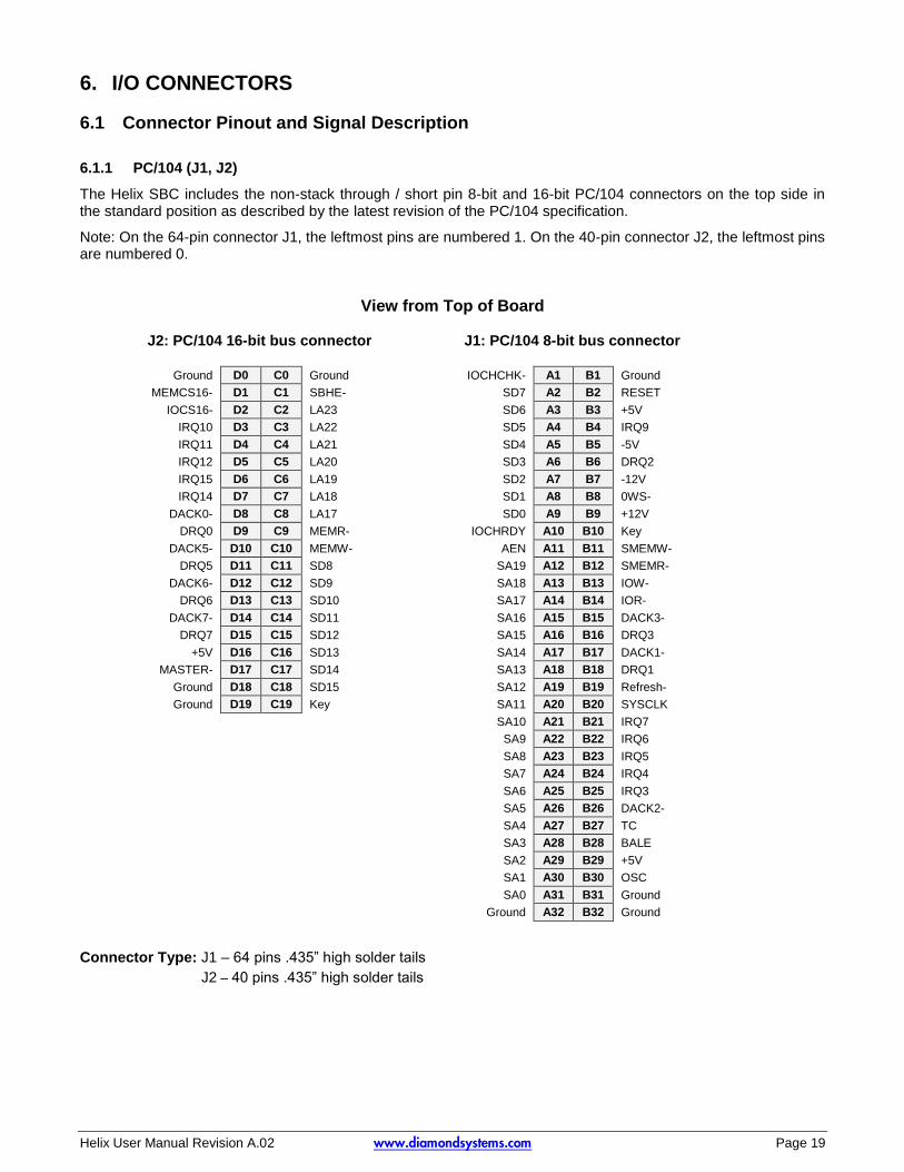
6.1.1 PC/104 (J1, J2)
The Helix SBC includes the non-stack through / short pin 8-bit and 16-bit PC/104 connectors on the top side in the standard position as described by the latest revision of the PC/104 specification.
Note: On the 64-pin connector J1, the leftmost pins are numbered 1. On the 40-pin connector J2, the leftmost pins are numbered 0.
View from Top of Board
J2: PC/104 16-bit bus connector J1: PC/104 8-bit bus connector
Ground D0 C0 Ground IOCHCHK- A1 B1 Ground
MEMCS16- D1 C1 SBHE- SD7 A2 B2 RESET
IOCS16- D2 C2 LA23 SD6 A3 B3 +5V
IRQ10 D3 C3 LA22 SD5 A4 B4 IRQ9
IRQ11 D4 C4 LA21 SD4 A5 B5 -5V
IRQ12 D5 C5 LA20 SD3 A6 B6 DRQ2
IRQ15 D6 C6 LA19 SD2 A7 B7 -12V
IRQ14 D7 C7 LA18 SD1 A8 B8 0WS-
DACK0- D8 C8 LA17 SD0 A9 B9 +12V
DRQ0 D9 C9 MEMR- IOCHRDY A10 B10 Key
DACK5- D10 C10 MEMW- AEN A11 B11 SMEMW-
DRQ5 D11 C11 SD8 SA19 A12 B12 SMEMR-
DACK6- D12 C12 SD9 SA18 A13 B13 IOW-
DRQ6 D13 C13 SD10 SA17 A14 B14 IOR-
DACK7- D14 C14 SD11 SA16 A15 B15 DACK3-
DRQ7 D15 C15 SD12 SA15 A16 B16 DRQ3
+5V D16 C16 SD13 SA14 A17 B17 DACK1-
MASTER- D17 C17 SD14 SA13 A18 B18 DRQ1
Ground D18 C18 SD15 SA12 A19 B19 Refresh-
Ground D19 C19 Key SA11 A20 B20 SYSCLK
SA10 A21 B21 IRQ7
SA9 A22 B22 IRQ6
SA8 A23 B23 IRQ5
SA7 A24 B24 IRQ4
SA6 A25 B25 IRQ3
SA5 A26 B26 DACK2-
SA4 A27 B27 TC
SA3 A28 B28 BALE
SA2 A29 B29 +5V
SA1 A30 B30 OSC
SA0 A31 B31 Ground
Ground A32 B32 Ground
Connector Type: J1 – 64 pins .435” high solder tails
J2 – 40 pins .435” high solder tails

Helix User Manual Revision A.02 www.diamondsystems.com Page 20
6.1.2 Audio (J3)
Audio signals are provided on connector J3 with following pinout.
LineOut-L 1 2 LineOut-R
GND_Audio 3 4 GND_Audio
LineIn-L 5 6 LineIn-R
GND_Audio 7 8 GND_Audio
MIC_L 9 10 MIC_R
Connector Type: Standard 2mm dual row straight pin header.
6.1.3 USB 2.0 Ports (J4, J5, J6) There are three USB 2.0 connectors with identical pinouts, J4, J5 and J6. Each connector provides access to two USB 2.0 ports for a total of six USB 2.0 ports.
Key 1 2 Shield
USB1 Pwr- 3 4 USB0 Pwr-
USB1 Data+ 5 6 USB0 Data+
USB1 Data- 7 8 USB0 Data-
USB1 Pwr+ 9 10 USB0 Pwr+
Connector Type: Standard 2mm dual row straight pin header.
6.1.4 Serial Ports (J7, J8)
There are two serial port connectors J7 and J8, supporting two ports per connector. Serial ports 1-2 support only RS-232 mode. Serial ports 3-4 support RS-232/485/422 modes.
RS-232
RS-422
TX1 1 2 RTS1
RX1 3 4 CTS1
GND 5 6 GND
TX2 7 8 RTS2
RX2 9 10 CTS2
TX1+ 1 2 TX1-
RX1+ 3 4 RX1-
GND 5 6 GND
TX2+ 7 8 TX2-
RX2+ 9 10 RX2-

Helix User Manual Revision A.02 www.diamondsystems.com Page 21
RS-485
Connector Type: Standard 2mm dual row straight pin header.
6.1.5 LCD Backlight (J9)
Connector J9 is used for the LCD backlight control. The input power source is user selectable using jumpers in jumper block JP5 to select +5V or +12V. Brightness is controlled over PWM (pin 6) on this connector. Options available are to set the PWM voltage level to 3.3V or 5V using jumper.
1 Power +5V/+12V, jumper selectable
2 Power (same as pin 1)
3 Ground
4 Ground
5 Enable (GPIO output), 0 = off, open circuit = on
6 PWM, 5V/ 3.3V level jumper selectable
Connector Type: 6 pin RA 1.25mm pitch SMD header (053261-0671 from Molex).
Mating Housing: 51021-0600
Crimp terminal: 50058-8000
6.1.6 Power In (J10)
Input power is supplied through connector J10.
Ground 1 2 +12V
Ground 3 4 +5V / VIN
Ground 5 6 +5V / VIN
Ground 7 8 +5V / VIN
+VIN = +9V to +36V for boards with the optional wide voltage input circuit.
Connector Type: Connector used is IPL1-104-01-L-D-RA-K.
6.1.7 External Battery (J11)
Connector J11 is available for use with an external battery.
1 VBAT
2 Ground
VBAT = +3.3V
Connector Type: Hirose DF13A-2P-1.25H right-angle friction lock pin header.
TX1/RX1+ 1 2 TX1/RX1-
NC 3 4 NC
GND 5 6 GND
TX2/RX2+ 7 8 TX2/RX2-
NC 9 10 NC
Helix User Manual Revision A.02 www.diamondsystems.com Page 22
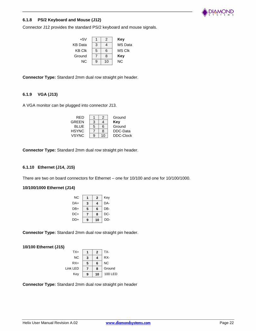
6.1.8 PS/2 Keyboard and Mouse (J12)
Connector J12 provides the standard PS/2 keyboard and mouse signals.
+5V 1 2 Key
KB Data 3 4 MS Data
KB Clk 5 6 MS Clk
Ground 7 8 Key
NC 9 10 NC
Connector Type: Standard 2mm dual row straight pin header.
6.1.9 VGA (J13)
A VGA monitor can be plugged into connector J13.
RED 1 2 Ground
GREEN 3 4 Key
BLUE 5 6 Ground
HSYNC 7 8 DDC-Data
VSYNC 9 10 DDC-Clock
Connector Type: Standard 2mm dual row straight pin header.
6.1.10 Ethernet (J14, J15)
There are two on board connectors for Ethernet – one for 10/100 and one for 10/100/1000.
10/100/1000 Ethernet (J14)
NC 1 2 Key
DA+ 3 4 DA-
DB+ 5 6 DB-
DC+ 7 8 DC-
DD+ 9 10 DD-
Connector Type: Standard 2mm dual row straight pin header. 10/100 Ethernet (J15)
TX+ 1 2 TX-
NC 3 4 RX-
RX+ 5 6 NC
Link LED 7 8 Ground
Key 9 10 100 LED
Connector Type: Standard 2mm dual row straight pin header

Helix User Manual Revision A.02 www.diamondsystems.com Page 23
6.1.11 Utility (J16) Utility connector J16 provides access to a variety of signals. The 3.3V pin is connected to the system 3.3V rail through a poly-switch resettable fuse. The fuse is rated for ~50mA maximum sustained current.
RESET BUTTON 1 2 PWM
GND 3 4 ETH2 ACT
I2C DATA 5 6 ETH2 LNK100
I2C CLOCK 7 8 ETH2 LINK1000
GND 9 10 3.3V (fused)
Connector type: Standard 2mm dual row straight pin header.
6.1.12 Digital I/O (J17) The DIO pins on the digital I/O connector provide access to jumper-selectable 3.3V / 5V system voltage rail through a polyswitch resettable fuse. The fuse is rated for ~100mA maximum sustained current.
The pinout definition for the DIO connector in Helix SBCs with the full data acquisition circuit (A model) is given below.
DIO A0 1 2 DIO A1
DIO A2 3 4 DIO A3
DIO A4 5 6 DIO A5
DIO A6 7 8 DIO A7
DIO B0 9 10 DIO B1
DIO B2 11 12 DIO B3
DIO B4 13 14 DIO B5
DIO B6 15 16 DIO B7
DIO C0 17 18 DIO C1
DIO C2 19 20 DIO C3
DIO C4 21 22 DIO C5
DIO C6 23 24 DIO C7
+5V/3.3V fused 25 26 Dground
The pinout definition for the DIO connector in Helix SBCs without the full data acquisition circuit (D model) is given below.
DIO A0 1 2 DIO A1
DIO A2 3 4 DIO A3
DIO A4 5 6 DIO A5
DIO A6 7 8 DIO A7
DIO B0 9 10 DIO B1
DIO B2 11 12 DIO B3
DIO B4 13 14 DIO B5
DIO B6 15 16 DIO B7
DX3 WDT 17 18 -
- 19 20 -
- 21 22 -
- 23 24 -
VIO(+5V/3.3V fused) 25 26 Dground

Helix User Manual Revision A.02 www.diamondsystems.com Page 24
Signal Name Definition
DIO A7-A0 Digital I/O port A; programmable direction
DIO B7-B0 Digital I/O port B; programmable direction
DIO C7-C0 Digital I/O port C; programmable direction; may be configured for counter/timer and PWM functions
+5V/3.3V Out Connected to switched +5V/3.3V supply via resettable fuse
Dground Digital ground; used for digital circuitry only
Connector type: Standard 2mm dual row straight pin header.
6.1.13 Analog I/O (J18)
Vout 0 1 2 Vout 1
Vout 2 3 4 Vout 3
Aground (Vout) 5 6 Aground (Vin)
Vin 0 / 0+ 7 8 Vin 8 / 0-
Vin 1 / 1+ 9 10 Vin 9 / 1-
Vin 2 / 2+ 11 12 Vin 10 / 2-
Vin 3 / 3+ 13 14 Vin 11 / 3-
Vin 4 / 4+ 15 16 Vin 12 / 4-
Vin 5 / 5+ 17 18 Vin 13 / 5-
Vin 6 / 6+ 19 20 Vin 14 / 6-
Vin 7 / 7+ 21 22 Vin 15 / 7-
DIO D0 23 24 DIO D1
DIO D2 25 26 Dground
Signal Name Definition
Vin 7/7+ ~ Vin 0/0+ Analog input channels 7 – 0 in single-ended mode; High side of input channels 7 – 0 in differential mode; high impedance inputs
Vin 15/7- ~ Vin 8/0- Analog input channels 15 – 8 in both single-ended mode; Low side of input channels 7 – 0 in differential mode;
Vout 3-0 Analog output channels 0 – 3
Aground (Vout), (Vin) Analog ground; used for analog circuitry only; Vout pin is optimized for the analog outputs; Vin pin is optimized for the analog
inputs
Dground Digital ground; used for digital circuitry only DIO D2-D0 Digital I/O port D; programmable direction
Connector type: Standard 2mm dual row straight pin header.

Helix User Manual Revision A.02 www.diamondsystems.com Page 25
6.1.14 SATA (J19) J19 can be used to connect to an external SATA hard drive or to mount an on-board SATA-DOM. Pin 7 is connected to a jumper that selects either Ground or 5VDC system voltage rail. Ground is used for an external storage device, and 5V is used for a board-mounted SATA-DOM flash-disk module. The 5V is connected via a resettable fuse.
1 Ground
2 SATA 1 TX+
3 SATA 1 TX-
4 Ground
5 SATA 1 RX-
6 SATA 1 RX+
7 Ground / 5V
Connector Type: 7-pin SATA connector, vertical.
6.1.15 CAN (J20) The CAN connector, J20, pinout is as shown below.
GND 1
CAN L 2
CAN H 3
GND 4
Connector type: SM04B-GHS-TB from JST
6.1.16 LVDS LCD (J21) J21 is the LCD connector. The pinout is shown below:
VDD 5V 1 2 VDD 5V
VDD 3.3V 3 4 VDD 3.3V
CLK+ Odd 5 6 CLK+ Even
CLK- Odd 7 8 CLK-Even
Ground 9 10 Ground
D0+ Odd 11 12 D0+ Even
D0- Odd 13 14 D0- Even
D1+ Odd 15 16 D1+ Even
D1- Odd 17 18 D1- Even
D2+ Odd 19 20 D2+ Even
D2- Odd 21 22 D2- Even
D3+ Odd 23 24 D3+ Even
D3- Odd 25 26 D3- Even
Ground 27 28 Ground
DDC CLK 29 30 DDC DATA
Connector Type: 30-pin connector from Hirose, DF13A-30DP-1.25V

Helix User Manual Revision A.02 www.diamondsystems.com Page 26
6.1.17 PCIe MiniCard / mSATA Socket (J24)
All TX/RX signals are with respect to the host. TX on the socket drives RX on the installed module, and RX on the socket is driven by TX on the installed module.
The two mounting standoffs at the far end of the module installation site are not connected to ground.
PCIe MiniCard mSATA mSATA / PCIe MiniCard
1 2 +3.3V
3 4 Gnd
5 6 +1.5V
Clkreq- 7 8
Gnd Gnd 9 10
PCIe 1 Clk- PCIe 1 Clk- * 11 12
PCIe 1 Clk+ PCIe 1 Clk+ * 13 14
Gnd Gnd 15 16
KEY
17 18 Gnd
19 20 Disable-
Gnd Gnd 21 22 PCIe Reset-
PCIe 1 RX- SATA 0 RX+ 23 24 +3.3V
PCIe 1 RX+ SATA 0 RX- 25 26 Gnd
Gnd Gnd 27 28 +1.5V
Gnd Gnd 29 30 SMB Clk
PCIe 1 TX- SATA 0 TX- 31 32 SMB Data
PCIe 1 TX+ SATA 0 TX+ 33 34 Gnd
Gnd Gnd 35 36
Gnd Gnd 37 38
+3.3V +3.3V 39 40 Gnd
+3.3V +3.3V 41 42 WWAN LED-
Ground Ground 43 44 WLAN LED-
45 46 WPAN LED-
47 48 +1.5V
Pull-up to +3.3V Pull-up to +3.3V 49 50 Gnd
51 52 +3.3V
Connector Type: 52-pin MiniCard, full size, with PCB mount threaded spacers

Helix User Manual Revision A.02 www.diamondsystems.com Page 27
6.2 List Of Connectors
The following table provides a summary of all I/O connectors on the Helix SBC.
Function Manufacturer Part Number Description Latching Connector Mating Cable
Power in Samtec IPL1-104-01-L-D-RA-K 2x4 box header T/H Right angle .1” pitch
- 6980512
External battery
Molex DF13A-2P-1.25H 2 pos. 1.27mm pitch, SMT
- 6980511
USB 2.0
Qty = 3 Pinnrex 222-9205GB01
2x5, 2mm pitch, SMT Header
98424-G52-10ALF 6981082
PS/2 Pinnrex 222-9205GB01 2x5, 2mm pitch, SMT Header
- 6981083
Serial ports
Qty = 2 Pinnrex 222-9205GB01
2x5, 2mm pitch, SMT Header
98424-G52-10ALF 6981075
Gigabit Ethernet
Pinnrex 222-9205GB01 2x5, 2mm pitch, SMT Header
98424-G52-10ALF 6981080
10/100 Ethernet
Pinnrex 222-9205GB01 2x5, 2mm pitch, SMT Header
98424-G52-10ALF 6981161
Audio Pinnrex 222-9205GB01 2x5, 2mm pitch, SMT Header
98424-G52-10ALF 6981076
Utility Pinnrex 222-9205GB01 2x5, 2mm pitch, SMT Header
98424-G52-10ALF 6981169
VGA Pinnrex 222-9205GB01 2x5, 2mm pitch, SMT Header
98424-G52-10ALF 6981084
Analog I/O Pinnrex 222-9213GB01 2x13, 2mm pitch, SMT Header
98424-G52-26ALF 6980515
Digital I/O Pinnrex 222-9213GB01 2x13, 2mm pitch, SMT Header
98424-G52-26ALF 6980515
CAN JST SM04B-GHS-TB 1x4, 1.25mm pitch, RA, SMT Header
- 6981182
SATA Molex 0678005025 7-pin SATA connector, SMT Vertical
- 6989101
SATA Power
Molex DF13A-2P-1.25H 2 pos. 1.27mm pitch, SMT
- Custom
LCD Hirose DF13A-30DP1.25V(55)
2x 15, 1.25MM SMT, Vertical
- Custom
LCD backlight
Molex 53261-0671 6 pos. 1.25mm pitch, SMT, RA
- Custom
PCIe MiniCard
JAE
MM60-52B1-E1-R650 +
NT4R1600 spacer
52-pin Minicard, full size, with PCB mount threaded spacers
- -
PC/104 – J1 Harwin* M20-6113245* 64 pins .435” high solder tails
- -
PC/104 – J2 Harwin* M20-6112045* 40 pins .435” high solder tails
- -
Helix User Manual Revision A.02 www.diamondsystems.com Page 28
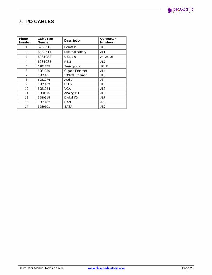
7. I/O CABLES
Photo Number
Cable Part Number
Description Connector Numbers
1 6980512 Power in J10
2 6980511 External battery J11
3 6981082 USB 2.0 J4, J5, J6
4 6981083 PS/2 J12
5 6981075 Serial ports J7, J8
6 6981080 Gigabit Ethernet J14
7 6981161 10/100 Ethernet J15
8 6981076 Audio J3
9 6981169 Utility J16
10 6981084 VGA J13
11 6980515 Analog I/O J18
12 6980515 Digital I/O J17
13 6981182 CAN J20
14 6989101 SATA J19

Helix User Manual Revision A.02 www.diamondsystems.com Page 29
8. JUMPER DESCRIPTION
Following drawing shows only the connectors and jumper blocks on the board. The default jumper positions are shown in red.
Figure 4: Default Jumper Locations
Jumper Description
JP1 Digital VIO
JP2 CAN Termination
JP3 Miscellaneous: SATA DOM, Boot Delay, Battery Disconnect, Single Channel LCD
JP4 RS-422/485 Termination
JP5 LVDS Backlight & LVDS VDD
JP6 IRQ Selection
JP1 JP3 JP2
JP5
JP6
JP4

Helix User Manual Revision A.02 www.diamondsystems.com Page 30
8.1 Digital IO (JP1)
The digital I/O can be pulled up to 5V/3.3V or pulled down to GND by configuring jumper block JP1. The jumper locations of this jumper block will also determine the input voltage to the DAQ circuit. By default the DIOs are pulled high to 3.3V. Figure 7 shows the default jumper locations of JP1.
Figure 5: Jumper Block JP1
The following table shows the different combinations of jumper block JP1. The row in bold and italics shows the default configuration of jumper block JP1.
L-P P-H 3-V V-5 DIO pull high/low
DIO Voltage
In Out In Out Low 3.3V
In Out Out In Low 5V
Out In In Out High 3.3V
Out In Out In High 5V
Note:
1. Jumpers should be installed in either positions 3-V or V-5 even if the jumper in position L-P is Out (DIO are pulled Low to GND) as this voltage is tied to the input voltage to the DAQ circuits.
8.2 CAN Termination (JP2)
Jumper block JP2 is used to enable 120 Ohm CAN termination.
Figure 6: Jumper Block JP3
B TL TH 120 Ohm Termination
In In In Enabled
Out Out Out Disabled

Helix User Manual Revision A.02 www.diamondsystems.com Page 31
8.3 Miscellaneous (JP3)
Figure 7: Jumper Block JP3
SATA
The 7th pin of the SATA connector, J19, can be configured for SATA DOM or for SATA cable. By default the 7
th
pin of J19 is connected to ground for the SATA cable. The default jumper location is shown in Figure 7.
The following table shows the valid combinations of jumper block JP3. The row in bold and italics shows the default configuration.
5V GND Description
Out In SATA_PIN7 = GND (SATA CABLE)
In Out SATA_PIN7 = 5.0V (SATA DOM)
Note: 5V and GND jumpers should never be inserted at the same time.
Boot Delay without RTC
Jumper block JP3 can also be used to delay the power good signal when the RTC battery is not installed. Boot up time is delayed by 5.7 sec when the RTC battery is not mounted. In models without a battery this jumper should be installed to assure proper boot-up.
DLY Description
Out No boot-up delay
In Boot up delay = 5.7 sec
Disconnect RTC battery
BAT Jumper in JP3 can be removed to prevent the RTC battery from draining during long term storage. The jumper should be inserted for normal operation.
BAT Description
Out Battery power is disconnected to avoid drainage
In RTC battery power is enabled

Helix User Manual Revision A.02 www.diamondsystems.com Page 32
Single channel LCD
By default, Helix supports dual channel LVDS displays. To support a single channel LVDS LCD, a jumper should be inserted in position LVDS.
8.4 RS-422/485 Termination (JP4)
Jumper JP4 is used to enable 120 Ohm termination for serial ports in RS-485 and RS-422 modes.
RS-485 Mode Termination Enabled RS-422 Mode Termination Enabled
Figure 8: Jumper Block JP4 Configurations
T3 R3 T4 R4 Mode
In Out In Out 120 Ohm Termination Enabled on pairs TX3 and RX3 (For RS-485 Mode)
In In In In 120 Ohm Termination Enabled on all four pairs (For RS-422 Mode)
Out Out Out Out Terminations Disabled (RS-232 Mode)
Note:
1. Do not install a jumper on 2-3, 4-5 and 6-7 positions.
LVDS Description
Out Dual channel LCD is used
In Single channel LCD is used

Helix User Manual Revision A.02 www.diamondsystems.com Page 33
8.5 LVDS Backlight and LVDS VDD (JP5)
Jumper block JP5 configures the voltage supply for the LCD backlight and for LVDS VDD. The orientation of the block in the diagrams matches the orientation of the jumper block when the board is rotated so that the PC/104 connector is on the lower edge.
Available options are +5V and +12V from the main power supply input. +12V is not used by any circuit on the Helix SBC. +12V is needed only for the LCD backlight, and the backlight is to be powered via the backlight power connector J9, hence +12V is supplied on the main power input connector along with +5V.
By default the LVDS backlight is provided with +12V and the LVDS VDD is provided with 3.3V. Figure 9 shows the default jumper locations.
Figure 9: Jumper Block JP5
The following table shows different combinations of jumper locations on JP5. The default configuration is the row in bold and italics.
12 5 5 3 LVDS Backlight
LVDS VDD
In Out In Out 12V 5V
In Out Out In 12V 3.3V
Out In In Out 5V 5V
Out In Out In 5V 3.3V
Note:
1. Voltage supply on LVDS backlight will not depend on or affect the voltage input of LVDS.
2. Do not install a jumper on 3-4 positions.
8.6 IRQ Selection (JP6)
JP6 is used for DAQ circuit IRQ selection. Based on the jumper position, either IRQ5 or IRQ7 will be used by the FPGA to interrupt the processor.
Figure 10: Jumper Block JP6
5 7 IRQ Selected
In Out IRQ5 is selected
Out In IRQ7 is selected

Helix User Manual Revision A.02 www.diamondsystems.com Page 34
9. BIOS KEY FEATURES
The Helix SBC BIOS provides access to many valuable features. These instructions show how to enter the BIOS and set up features.
9.1 Entering the BIOS
The BIOS may be entered during startup by pressing the DEL key on an attached keyboard. Press the key repeatedly soon after a power-on or reset until the BIOS screen appears. After a specific period of time during startup (generally a few seconds), the BIOS will ignore the DEL key. If the system does not respond as expected after pressing the DEL key, the user can simply reset the board (or power down) and try again.
9.2 Restoring Default BIOS Settings
While making changes to the BIOS settings, the new settings are stored in SPI flash internal in the Vortex86DX3 processor. If the user wants to restore the BIOS settings to the default state, follow the procedure listed below.
1. Connect a keyboard to the USB keyboard port or PS/2 keyboard port and connect a monitor.
2. Reboot the CPU (reset or power-down and power-up).
3. Hold down the END key while the CPU is booting.
4. The board will boot up normally. The BIOS settings will be reset to their defaults.
End key functionality also works in the BIOS menu. When the BIOS menu is displayed, press the end key.
9.3 Upgrading BIOS using DOS Utility
The BIOS resides in the internal flash of the DX3 and can be updated using a DOS utility (ANYBIOS.exe). The BIOS image and ANYBIOS utility should be present in the DOS bootable USB pen drive connected to the board.
Follow the below steps to re-flash/ upgrade the BIOS
1. Save the BIOS file and ANYBIOS utility in a DOS bootable pen drive.
2. Connect this pen drive to any one of the USB ports in Helix.
3. Power on the board and boot the board to DOS.
4. Open the folder containing the BIOS file and ANYBIOS utility using command: cd “folder name”
5. In DOS, for updating the BIOS, execute the command:
anybios w “BIOS FILE NAME”.rom skipmac OR
anybios w “BIOS FILE NAME”.bin skipmac
6. Upon flashing the BIOS successfully, restart the board to boot from the new BIOS.
Warring: Before flashing the BIOS, ensure that the pen drive has the correct BIOS image. If an incorrect/ corrupt BIOS image is flashed, the board may not boot again. Contact Diamond Systems for the latest BIOS image.
9.4 Setting the Date and Time
To set the date and time in the BIOS, select the Main menu, then enter the date and time at the top of the screen. This screen also displays the CPU speed and memory capacity of the board.
9.5 Boot Priority
To select Boot devices and priority, go to the Boot menu and select Boot Device Priority. The user can change the boot devices priority in this screen.

Helix User Manual Revision A.02 www.diamondsystems.com Page 35
9.6 LED
A green BIOS LED indicates that the SBC has been booted to the BIOS GUI. The location of the BIOS LED is shown in the Board Layout Section.
9.7 Watchdog Timer
The watchdog timer can be used to generate a system reset upon the expiration of a programmed time interval.
The watchdog timer can be enabled in BIOS. To enable it, go to the Advanced settings menu and then the Watchdog timer configuration. The user can enable the watchdog timer and select the function as reset. The timeout period can also be selected here. The watchdog timer circuit timeout period is programmable from 10 milliseconds to 512 seconds.
9.8 Quiet / Quick Boot / Splash Screen
Quiet boot replaces the system status and configuration screen that appears during startup with a blank screen or custom splash screen (if available). Quick boot turns off the memory test during startup to save time. To enable these features, go to the Boot menu, then select Boot Settings Configuration. Diamond Systems can provide custom splash screens upon request in the form of an image file.
9.9 Serial Port Configuration
The Helix SBC supports four serial ports. Ports 1 and 2 support RS-232 functionality. Ports 3 and 4 support RS-232/422/485 functionality. Ports 3 and 4 can be configured from the BIOS GUI. In the BIOS setup go to the Advanced menu and select the Serial/Parallel port configuration. Select the appropriate mode for Ports 3 and 4.

Helix User Manual Revision A.02 www.diamondsystems.com Page 36
10. GETTING STARTED
This section describes the steps needed to get your Helix SBC up and running and assumes that you also have a Helix Development Kit or Helix Cable Kit. The Cable Kit includes all cables needed for most I/O, except the LCD and backlight. The Development Kit includes the Cable Kit, and a pre-programmed mSATA DOM.
10.1 Development Kit Contents
Model Number Description
HLX1000-XXX Helix SBC
CK-HLX-01 Helix Cable Kit for most on board I/O
32GB MLC SATA-DOM flash-disk with bootable image
Helix Development kit user manual
10.2 Quick Setup
1. Attach the VGA cable 6981084, PS/2 keyboard / mouse cable 6981083, and USB cables 6981082 as needed.
2. Attach display, keyboard, and mouse (if needed) to the cables.
3. Check the jumpers as described in Section 7 for a default settings or change as desired.
4. Connect power to power input connector J10 using your own power supply with power cable 6980512. The input connector and cable are keyed to prevent incorrect connection.
WARNING: Attaching the power connector incorrectly will destroy the Helix SBC!
For a quick verification that the system is set up and working properly, if no boot device is attached, the system will boot to FreeDOS on the on-board virtual flash drive. In order for this to work, the on-board flash drive must be enabled.
10.3 Boot Device Options
Helix can boot from SATA or any of the available USB ports or PXE (10/100 Ethernet port only). Either a board powered SATA DOM or an externally powered SATA HDD can be connected to the SATA port. Diamond Systems’ software and hardware development kits include a SATA DOM with pre-loaded OS.
Helix can boot to a SATA device or a USB device. Helix can be booted from the flash-disk provided by Diamond Systems or from an external hard drive.
WARNING: It is possible to destroy the Helix SBC by connecting a SATA cable incorrectly (reverse orientation or offset from correct position). Always use keyed cables to avoid connection errors.
The Boot device selection and priority are configured in the BIOS Boot menu. Only devices which are connected to the SBC will appear in the list of options. Therefore if user wants to select a hard drive or USB device as the boot device, the SBC should be connected first, then boot up, enter the BIOS, and select the desired device as the boot device.
Note: Board does not support booting from mSATA port.

Helix User Manual Revision A.02 www.diamondsystems.com Page 37
The following are a few examples of boot scenarios.
Install an externally powered SATA hard drive directly on the SATA connector
Attach a SATA DOM on the SATA connector (the Helix SBC will provide power to the SATA DOM via Jumper block JP2, pins 1-2)
Attach an mSATA device on the shared mSATA / PCIe MiniCard socket
Attach a bootable USB device to one of the USB ports
PXE boot (supported by the 10/100 Ethernet port only)
10.4 Installing OS and Booting
The following steps describe how to install an operating system from an external SATA hard disk drive.
An external SATA HDD requires power and data cables to be connected to it. The data cable connects the Helix SBC to the HDD. Power to the HDD should be sourced from an external power supply.
Follow the below steps to install a 32-bit Windows 7 operating system on a SATA HDD.
Connect a USB pen drive to a USB port of (J4) Helix SBC having 32-bit Windows 7 installation image.
Power ON the board
Enter the BIOS menu by pressing DEL key. The SATA HDD and USB device should be detected in BIOS under boot devices.
Under boot priorities, set the highest priority for USB.
Save the BIOS settings and restart.
The Windows 7 installer will start running. Follow the instructions to complete the installation.
Upon successful installation, boot to Windows 7 and install the necessary drivers.
Upon restart, to boot from SATA HDD, go to BIOS menu and under boot priorities set highest priority to Hard disk.

Helix User Manual Revision A.02 www.diamondsystems.com Page 38
11. VIDEO FEATURES
The Helix SBC supports VGA and LVDS LCDs as display device options.
11.1 VGA
The VGA display can be set as primary or secondary display using the graphic utility in Windows 7 OS. If the VGA is set as primary display, the VGA display will be active in both the BIOS and OS. The maximum VGA resolution is 1920x1440 at 60Hz.
11.2 LCD
An LCD display is realized using the LVDS interface. A RGB to LVDS converter provides a dual-channel LVDS LCD output. The LCD can be used as the primary display by using the graphic utility in Windows 7 OS. If the LCD is set as primary display, the LCD display will be active in both the BIOS and OS. The maximum LCD resolution is 1920x1440 at 60Hz.
11.2.1 Backlight
The LCD backlight control is provided by a PWM circuit. LCD backlight power and control are on a separate latching connector. An option is provided to change the duty cycle and frequency from BIOS menu (Advanced menu - LCD Backlight Control).
From the BIOS menu, the frequency of the PWM signal can be set as 100Hz, 200Hz, 500Hz, 1KHz, 2KHz, 5KHz, 10KHz and 20KHz. Default is 1KHz.
On models without the full data acquisition circuit (D model), the BIOS menu allows the user to set the PWM duty cycle to 50% or 100%. On models with full data acquisition (A model), the PWM duty cycle can be varied from 30% to 100% in intervals of 10%. Once the operating system is loaded, the application can change the duty cycle from 1% to 100%.
A jumper is provided to set the PWM voltage to 3.3V or 5V. See Jumper Description section for more details.
11.3 Dual Display
The Helix SBC supports dual display operation, meaning the VGA and LCD displays are active at same time. To support this feature, a graphic utility driver developed by DMP Electronics has to be installed in Windows 7. The display can be either duplicated or extended to the second display device.
To set the LCD as the primary display, connect the LCD to the Helix SBC before power on. Do not connect the VGA cable. Boot the SBC to Windows 7 OS and check the graphics utility. The LCD should be enabled under the display devices menu. Now connect the VGA cable. The display will execute hot plug functionality and the VGA display will become active. Open the graphics utility and enable the LCD. The VGA and LCD display will become active.
To extend the display from the LCD to the VGA monitor, set the LCD as display option 1. Right click on the desktop and select screen resolution. Under display option, select Monitor option 2. Now the display will be extended to the VGA monitor.
To set the VGA as the primary display, connect the VGA cable to SBC and power on. The VGA display will be active in the BIOS as well as the OS. In the graphics utility tool, the CRT option will be enabled under the display devices menu. The display can be duplicated in the LCD by enabling the LCD option.
To extend the display from the VGA to the LCD, set the CRT as display option 1. Right click on the desktop and select screen resolution. Under display option, select option 2. Now the display will be extended to the LCD.
Helix User Manual Revision A.02 www.diamondsystems.com Page 39
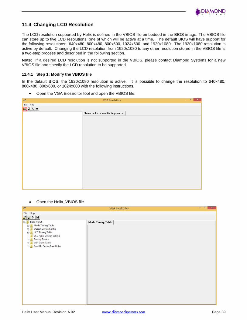
11.4 Changing LCD Resolution
The LCD resolution supported by Helix is defined in the VBIOS file embedded in the BIOS image. The VBIOS file can store up to five LCD resolutions, one of which will be active at a time. The default BIOS will have support for the following resolutions: 640x480, 800x480, 800x600, 1024x600, and 1920x1080. The 1920x1080 resolution is active by default. Changing the LCD resolution from 1920x1080 to any other resolution stored in the VBIOS file is a two-step process and described in the following section.
Note: If a desired LCD resolution is not supported in the VBIOS, please contact Diamond Systems for a new VBIOS file and specify the LCD resolution to be supported.
11.4.1 Step 1: Modify the VBIOS file
In the default BIOS, the 1920x1080 resolution is active. It is possible to change the resolution to 640x480, 800x480, 800x600, or 1024x600 with the following instructions.
Open the VGA BiosEditor tool and open the VBIOS file.
Open the Helix_VBIOS file.

Helix User Manual Revision A.02 www.diamondsystems.com Page 40
Expand LCD Timing Table. Resolutions 640x480, 800x480, 800x600, 1024x600, and 1920x1080 are listed under this menu. Note: If your LCD resolution is not in the list, please send the LCD datasheet to Diamond Systems for new VBIOS ROM.
Choose the desired LCD resolution from the menu LCD Panel Default Setting. By default 1920x1080 is the standard LCD setting set in the Helix BIOS.
Save the new VBIOS.

Helix User Manual Revision A.02 www.diamondsystems.com Page 41
11.4.2 Step 2: Integrate the VBIOS with the BIOS file
In order to take effect, the new VBIOS has to be integrated with the existing BIOS image. This is done using a utility called MMTOOL.EXE.
The following items are required to modify the BIOS image:
1. PC with MMTOOL software
2. Existing Helix BIOS image
3. Helios LCD VBIOS file
4. Bootable USB memory stick with DOS
5. ANYBIOS utility saved in DOS bootable USB memory stick.
Instructions for MMTOOL software:
1. Start the MMTOOL software on the Windows computer.
2. Click on the “Load ROM” button.
3. Select the latest BIOS image file from the table above and click on the “Open” button. The following screen will appear:

Helix User Manual Revision A.02 www.diamondsystems.com Page 42
4. Go to Replace, Load new VBIOS file to be integrated. Select the VBIOS module on 17F3:2015 indicated by arrow, and press “Replace.”
5. Save the new BIOS.
Refer to the section “Upgrading BIOS Using DOS Utility” for instructions on how to flash the new BIOS.

Helix User Manual Revision A.02 www.diamondsystems.com Page 43
12. SERIAL PORTS AND SYSTEM CONSOLE
12.1 Overview
Helix SBC supports total 4 serial ports. Port 1 and 2 supports RS-232 mode. Port 3 and 4 support RS-232/422/485 modes. The modes for Port 3 and 4 can be configured in BIOS. In RS-422 and RS-485 mode, 120 ohm line termination can be enabled using Jumper Block JP4.
12.2 Configuration
The serial port settings can be configured from the BIOS menu. Under the Advanced menu select Serial Port Configuration to modify the address, IRQ level, baud rate, and protocol. The default settings are shown below.
Port I/O Address IRQ Baud Rate Protocol
COM1 0x3F8 4 115200 RS-232
COM2 0x2F8 3 115200 RS-232
COM3 0x3E8 6 115200 RS-232
COM4 0x2E8 12 115200 RS-232
I/O Address and IRQ: Each serial port requires 8 bytes of address space starting with the base address selected. For example, an address of 3F8 means an address range of 3F8 – 3FF.
Always select a unique address and IRQ value for each port. Selecting the same value for more than one port will cause a conflict and lead to unpredictable behavior in the operating system.
Baud Rate: BIOS menu allows configuration of each port for baud rates (bps) of 2400, 4800, 9600, 19200, 38400, 57600, or 115200.
Protocol: Serial ports 3 and 4 can be configured for RS-232, RS-485 or RS-422 protocols. Serial ports 1 and 2 operate only in RS-232 mode.
12.3 Console redirection
In many applications without a local display and keyboard, it may be necessary to obtain remote keyboard and monitor access to the SBC for configuration, file transfer, or other operations. Helix supports this activity by enabling keyboard input and character output onto a serial port, referred to as console redirection. In the Helix default BIOS configuration, console redirection is disabled.
A serial port on the remote PC can be connected to the serial port on Helix with a null modem cable. A null modem cable has a DB9 female connector at each end and swaps the TX and RX signals from one end to the other, so that two DTE devices can communicate directly with each other. PC serial ports are normally configured for DTE pinout. A terminal emulation program, such as HyperTerminal, running on the other computer can be used to establish the connection and communicate with Helix. The serial port configuration on the remote PC should match the serial port configuration of Helix (protocol, baud rate, etc).
Console redirection can be enabled in the BIOS with the following steps:
Enter the BIOS menu during power-up or reset by pressing DEL key.
Select the Advanced menu with the left/right arrow keys.
In Remote access configuration tab select “enable”.
In Serial Port Number, select COM1, COM2, COM3, or COM4. Save and restart the SBC.
Upon pressing DEL key, the user should see the BIOS setup menu in the remote PC terminal emulation application.

Helix User Manual Revision A.02 www.diamondsystems.com Page 44
13. MASS STORAGE
The Helix SBC can use a wide variety of mass storage options, both on-board and off-board. These options include external SATA hard disk drives, a board-mounted SATA DOM or mSATA flashdisks, or external USB hard drives.
13.1 Flashdisk Models and Capacities
Diamond Systems offers the following extended temperature SATA DOM and mSATA flashdisks for use with Helix SBCs.
Model Number Description
FDSM-64G-XT 64GB SATA DOM MLC Flashdisk
FDSM-32G-XT 32GB SATA DOM MLC Flashdisk
FDSS-64G-XT 64GB SATA DOM SLC Flashdisk
FDSS-32G-XT 32GB SATA DOM SLC Flashdisk
FDMM-64G-XT 64GB mSATA MLC Flashdisk
FDMM-32G-XT 32GB mSATA MLC Flashdisk
FDMM-16G-XT 16GB mSATA MLC Flashdisk
FDMS-64G-XT 64GB mSATA SLC Flashdisk
FDMS-32G-XT 32GB mSATA SLC Flashdisk
FDMS-16G-XT 16GB mSATA SLC Flashdisk
FDMS-8G-XT 8GB mSATA SLC Flashdisk
13.2 Installation and Configuration
To install any of the above SATA flashdisk devices, locate the desired SATA DOM (J19) or mSATA (J24) ports on the Helix SBC. Plug the flashdisk module into the appropriate port. Remove the screw(s) from the mounting stand-off(s) before installing the flashdisk. Install the flashdisk and secure it to the Helix SBC with the screw(s) once the flashdisk is installed.

Helix User Manual Revision A.02 www.diamondsystems.com Page 45
14. UTILITY CONNECTOR FEATURES
A 2x5 pin header, J16, is provided on the SBC which gives access to I2C, PWM, reset and Gigabit Ethernet LED signals. The pinout of the utility connector is given below.
RESET - 1 2 PWM
GND 3 4 ETH2 ACT-
I2C DATA 5 6 ETH2 LNK100-
I2C CLOCK 7 8 ETH2 LINK1000-
GND 9 10 3.3V (fused)
Details for each of these interfaces are provided below.
14.1 I2C
The I2C interface from the Vortex SoC can be accessed over the utility connector. The I2C clock is connected to pin 7 and I2C data is connected to pin 9 of the utility connector. These signals are pulled up to 3.3V over a 10K resistor. There are no on-board devices connected to this I2C bus. Typical devices that can be connected to the I2C bus includes temperature sensor, EEPROM, I/O expanders etc.
14.2 Reset
The Helix SBC can be reset using the Reset- signal on pin 1 of the utility connector. Reset- is an active low signal and must be connected to Ground (Pin 3 or pin 9) to reset the device. The typical reset period is 10mS. Reset- has a weak pull up resistor (100K Ohm) to 3.3V on board. For normal functioning, the signal should be left floating.
Warning: It is not recommended to reset the board when the operating system is running as this may corrupt the hard disk.
14.3 Gigabit Ethernet LED Signals
LED signals for the Gigabit Ethernet (J14) are made available on the utility connector. The signals are used to indicate the status of the Gigabit Ethernet port. All the three signals are active LOW. Description for these signals are given below.
Activity
(ETH2 ACT-)
Link 100
(ETH2 LINK100-)
Link 1000
(ETH2 LINK1000-)
Description
Blink OFF OFF Port is active
Speed is 10 Mbps
Blink ON OFF Port is active
Speed is 100 Mbps
Blink ON ON Port is active
Speed is 1000Mbps
The Gigabit Ethernet LED signals are also connected to on-board LEDs, details are given in the LED section.
14.4 Power and Ground
Pin 10 of the utility connector is 3.3V power output and pins 3, 9 are digital ground. A PTC fuse is provided in series with the 3.3V output pin to limit the current draw to 100mA. The 3.3V power rail can be used to power an I2C device, to drive Gigabit Ethernet LEDs, or for any other requirement requiring less than 100mA current.

Helix User Manual Revision A.02 www.diamondsystems.com Page 46
15. A MODEL DATA ACQUISITION CIRCUIT
15.1 Features
Helix “A” models include a complete data acquisition circuit with a combination of analog and digital I/O features. The circuit controller is an FPGA that interfaces to the Vortex86DX3 processor via the SPI bus for data I/O and via the ISA bus for interrupt operation.
A/D Features
16 analog voltage inputs
16-bit resolution (1 part in 65536)
Programmable input ranges: 0-5V, 0-10V, +/-5v, +/-10V
Single-ended and differential input configuration options
Precision, low-drift 2.5V reference voltage
100KHz maximum total A/D sample rate (all active channels combined)
Integrated 2048-sample FIFO and interrupt service for efficient high-speed sampling
D/A Features
4 analog voltage outputs
16-bit resolution (1 part in 65536)
Single-channel and multi-channel simultaneous update modes
Programmable output range: 0-5V, 0-2.5V
30KHz update rate capability
Waveform generator on 1 to 4 outputs with user-defined waveforms and 2048-sample waveform buffer
Digital I/O features
27 digital I/O lines
User-selectable 3.3V / 5V logic levels
User-selectable 10K pull-up / pull-down resistors
Programmable direction in 8-bit and 1-bit groups
8-bit programmable edge detection circuit
Buffers for protection and higher current drive
8 32-bit counter/timers with up counting, down counting, pulse output, and interrupt features
4 24-bit pulse-width modulators with programmable duty cycle and output polarity
Interrupt support on ISA bus for A/D, digital I/O, and counter/timer circuits

Helix User Manual Revision A.02 www.diamondsystems.com Page 47
15.2 Block Diagram
Figure 11: Data Acquisition Circuit Block Diagram
15.3 Analog-to-Digital Circuit
15.3.1 A/D Circuit Overview
Helix “A” models include an analog input circuit based on the LTC1859 16-bit A/D converter, or ADC. The LTC1859 is capable of operating at up to 100,000 samples per second in total, either on a single channel or on any number of channels. The ADC supports programmable input ranges of 0-5V, 0-10V, +/-5V, and +/-10V. The input range can be changed on a sample by sample or channel by channel basis.
The LTC1859’s performance is improved by the addition of several external components. The LTC1859 includes a built-in channel multiplexor. However this multiplexor is bypassed in order to use an external circuit with increased channel count and higher input impedance. One pair of input channels is fed by two 8-channel multiplexors that can be configured for either 16 single-ended or 8 differential inputs. The ADC voltage reference is driven by an external precision 2.5V reference chip with higher initial accuracy and lower temperature drift than the LTC1859’s built-in reference. This helps to reduce gain errors in A/D measurements.
In single-ended mode, each channel is measured with respect to analog ground, i.e. the input signal must be connected between the input pin and the analog ground pin on the I/O connector. In differential mode, the voltage is measured as the difference between the two input pins, and the analog ground pin is not part of the measurement. When operating in single-ended mode, the two native input channels are expanded to 16 single-ended channels, and when operating in differential mode, the two channels are expanded to 8 differential channels.

Helix User Manual Revision A.02 www.diamondsystems.com Page 48
15.3.2 A/D Channel Selection, Sampling, and Timing
A/D conversions may be triggered by several sources, including a software command, a programmable clock in the circuit’s FPGA, and an external digital signal connected to one of the board’s digital I/O ports. These options provide maximum flexibility in tailoring the circuit’s performance to a wide variety of real-world applications. Software triggering is mostly used for low-speed sampling needs or where the exact elapsed time between samples is not critical. External triggering is used when the A/D sampling must be synchronized to some external activity such as a rotary or linear encoder. Clock timing is used for high speed sampling or where the time between samples must be precise.
A channel sequencer circuit in the FPGA controls which channels sampled by the ADC. The sequencer can be programmed to select any single channel repeatedly, or it can be programmed to select any consecutive group of channels. As described above, the A/D front end consists of two 8-channel multiplexors connected to two analog inputs of the ADC. In single-ended mode, the channel sequencer will treat the 16 inputs as channels 0-15 with reference to analog ground, and in differential mode the sequencer will treat them as 8 differential channels, with channels 0-7 forming the high side of the inputs (renamed as channels 0+ to 7+) and channels 8-15 forming the low side of the inputs (renamed as channels 0- to 7-).
The sequencer works in conjunction with two available sampling modes called sample and scan. In sample mode, each A/D clock or trigger event causes one A/D conversion to occur. If the sequencer is programmed for a single channel, each successive A/D conversion will sample the same channel. This method is useful for high speed sampling of an AC signal. If the sequencer is programmed for a range of channels, then each successive A/D clock will cause the next channel in the selected range to be sampled, with the result that all the selected input channels are sampled one at a time in round robin fashion.
In scan mode, each A/D clock generates one A/D conversion on all channels selected by the sequencer (called the scan range) in tight succession. This method is typically used with the programmable clock circuit to measure a group of channels all at once. The number of selected channels is called the scan size. The timing of scan mode differs significantly from sample mode in that all selected channels are sampled as closely together as possible in time instead of being spread out equally in time as is done in sample mode. The analog input circuit does not support simultaneous sampling mode, where all inputs are sampled at exactly the same time.
One very important fact to remember is that because scan sampling generates one A/D conversion for every channel in the scan range, the total sample rate of the circuit is equal to the clock rate times the scan size. This total sample rate must be kept at or below the hard 100KHz limit of the A/D converter.
A second very important fact is that the fastest possible sample rate for any channel is 100KHz divided by the scan size in scan mode or the number of selected channels in sample mode. Thus it is not possible to sample more than one channel at 100KHz. If two channels are selected, the maximum sample rate for each channel is 50KHz, and so on.
15.3.3 A/D FIFO and High Speed Sampling
The FPGA contains a 2048 sample FIFO which supports high-speed A/D sampling. The FIFO enables the CPU to avoid having to respond every time an A/D conversion occurs, which would consume too much processor time when high speed sampling is being executed. Instead, the A/D samples are stored in the FIFO, and when the number of samples reaches a user-defined threshold, an interrupt occurs on the ISA bus. The software can then respond to the interrupt and read out a large number of samples all at once. The Diamond Systems Universal Driver software provides full support for high speed A/D sampling with FIFO and interrupt support. Please refer to that user manual for operating details. When using Universal Driver software, the interrupt rate is equal to the total A/D sample rate divided by the programmed FIFO threshold, because each time the interrupt service routine runs, it will read out the number of samples equal to the threshold value. The threshold is programmable so that the application software can optimize the interrupt rate for its needs. In general the interrupt rate should not exceed 1KHz, and in most cases an interrupt rate of 100-200Hz is recommended.

Helix User Manual Revision A.02 www.diamondsystems.com Page 49
15.3.4 A/D Operation
In essence, an A/D converter converts an analog voltage to a number that indicates the ratio between that voltage and the full range of voltages that the A/D can measure. A 16-bit A/D converter means that all input voltages are represented by a 16-bit binary number ranging from 0 to 65535 (2
16-1), or binary 0000 0000 0000 0000 to 1111
1111 1111 1111. There are two groups of input ranges, unipolar and bipolar. Unipolar ranges consist of only positive voltages (0-5V, 0-10V), and bipolar ranges include both negative and positive voltages (+/-5V, +/-10V). For a unipolar input range, the A/D values are straight binary and will range from 0 (binary 0000 0000 0000 0000) for 0V to 65535 (binary 1111 1111 1111 1111) for the top end of the range. For a bipolar input range, the A/D values are 2s complement and will range from -32768 ( binary 1000 0000 0000 0000) to +32767 (binary 0111 1111 1111 1111).
The tables below summarize the relationship between input voltage and A/D values for the general case. Note that the nominal upper limit of the input range (5.0000V or 10.0000V) is not achievable, since this voltage would require a 17 bit number (2
16 or 1 0000 0000 0000 0000). VFS means the full-scale input voltage, either 5V or 10V.
Bipolar Input Ranges
A/D Code A/D code binary Formula +/-5V input range +/-10V input range
-32768 1000 0000 0000 0000 -VFS -5.0000V -10.0000V
-32767 1000 0000 0000 0001 -VFS + 1 LSB -4.9998V -9.9997V
-1 1111 1111 1111 1111 -1 LSB -0.153mV -0.305mV
0 0000 0000 0000 0000 0V 0.0000V 0.0000V
1 0000 0000 0000 0001 +1 LSB 0.153mV .305mV
32767 0111 1111 1111 1111 VFS - 1 LSB 4.9998V 9.9997V
Unipolar Input Ranges
A/D Code A/D code binary Formula 0-5V input range 0-10V input range
0 0000 0000 0000 0000 0V 0.0000V 0.0000V
1 0000 0000 0000 0001 1 LSB (VFS / 65536) 0.076mV 0.153mV
32767 0111 1111 1111 1111 VFS / 2 - 1 LSB 2.4999V 4.9998V
32768 1000 0000 0000 0000 VFS / 2 2.5000V 5.0000V
32769 1000 0000 0000 0001 VFS / 2 + 1 LSB 2.5001V 5.0002V
65535 1111 1111 1111 1111 VFS - 1 LSB 4.9999V 9.9998V
15.3.5 A/D Resolution
The smallest change in input voltage that can be detected is 1/(216
), or 1/65536, of the full-scale input range. This smallest change results in an increase or decrease of 1 in the A/D code, and is referred to as 1 LSB (1 Least Significant Bit). The resolution is always 16 bits, but the value of 1 LSB will vary with the input range.
Polarity Input Range Resolution (1LSB)
Bipolar ±10V 305µV
Bipolar ±5V 153µV
Unipolar 0 - 10V 153µV
Unipolar 0 - 5V 76µV

Helix User Manual Revision A.02 www.diamondsystems.com Page 50
15.3.6 Input Range Selection
The input range of the A/D circuit is programmable in software and can be selected from the 4 values shown in the table above. Refer to the Universal Driver software user manual A/D section for details. The input range can be changed anytime, so that you can use different ranges for different input signals based on the best match. In general, you should select the highest gain (smallest input range) that allows the A/D converter to read the full range of voltages over which the input signals will vary. For example, if you have a signal that ranges from 0V minimum to 3V maximum, use the 0-5V range for best resolution. An input range that is too small causes the A/D converter to clip at either the high end or low end, and you will not be able to read the full range of voltages on your input signals.
15.3.7 Converting A/D Readings to Volts or Engineering Units
The A/D always returns a 16-bit binary number that represents the value of the input voltage relative to the selected input range. This number needs to be converted to a meaningful value in order to be used in your application. The first step is to convert it back to the actual measured voltage. Afterwards, you may need to convert the voltage to some other engineering units such as temperature in degrees C or weight in grams.
Since there are many possible formulas for converting the input voltage to engineering values, this secondary step is not described here. Only conversion to input voltage is described. However, you can combine both voltage and engineering unit conversions into a single formula if desired.
To convert the A/D value to its corresponding input voltage, use the following formulas.
Conversion Formula for Bipolar Input Ranges
Input voltage = A/D value / 32768 * Full-scale input voltage
where the A/D value is a 2s complement number ranging from -32768 to 32767, and the full-scale voltage is the nominal maximum value, either 5V or 10V. Example:
For bipolar input range ±5V, full-scale input voltage = 5V
For an A/D value of 17761: Input voltage = 17761 / 32768 * 5V = 2.710V
For an A/D value of -12345: Input voltage = -12345 / 32768 * 5V = -1.884V
Conversion Formula for Unipolar Input Ranges
Input voltage = A/D value / 65536 * Full-scale input voltage
where the A/D value is a straight binary number ranging from 0 to 65535, and the full-scale voltage is the nominal maximum value, either 5V or 10V. Example:
For unipolar input range 0-5V, full-scale input voltage = 5V.
For an A/D value of 17761: Input voltage = 17761 / 65536 * 5V = 1.355V

Helix User Manual Revision A.02 www.diamondsystems.com Page 51
15.3.8 Measurement Accuracy and Calibration
Although the A/D circuit has 16-bit resolution (meaning it can resolve input voltages to within 1/216
or 1/65536 of its input range), The measurement accuracy is not necessarily the same. All A/D circuits exhibit two inherent errors known as offset and gain errors. In addition all A/D circuits will experience some minor drift as the ambient temperature changes, as well as lesser drift over long periods of time.
To minimize the size and cost of the A/D circuit while still providing reasonable performance, the A/D circuit on Helix does not provide calibration features to eliminate these errors. Instead the circuit was designed to minimize the inherent offset, gain, and drift characteristics. The specifications at the end of this manual indicate the worst case offset, gain, and temperature drift errors in the circuit. Most boards will exhibit errors much lower than these values (typically 25-50% of the published values), so the A/D measurements can typically be used satisfactorily in your application without concern.
If higher accuracy is required, a software or digital calibration technique can be implemented in your application. Measure two known voltages close to the lower and upper limits of the input range you are using. The ideal values are between 1% and 5% at the bottom end and 95% and 99% at the top end. Compare the actual A/D readings of these input voltages to the expected values, and then store the differences in a file. Then you can use these errors to apply an offset and gain factor to each A/D reading on that board forevermore. Although this technique does not eliminate temperature and drift errors, it will eliminate the largest portion of the total error and provide more accurate measurements and better overall product performance.
When considering accuracy, it is important to consider all the contributions to measurement error. In addition to the inherent A/D errors, the sensors connected to the A/D also have their own offset, gain, and temperature/time drift errors. Usually these errors will be published as a simple accuracy figure in a percentage form. One percent error on a 16-bit A/D is 655 LSBs, so if your sensor has a 1% error specification, that is already more than 10x the typical A/D reading error, and therefore software calibration of the A/D readings alone will not provide any material benefit. However the same technique described above can be applied with the sensor connected using known input conditions (for example empty scale and scale with a precision weight applied), so that you can eliminate total system error.
To include A/D error values into the input voltage calculation, use this formula:
Input voltage = ((ADC – Cmin) / (Cmax – Cmin)) * (Vmax – Vmin) + Vmin
ADC = A/D code Vmax = Test input voltage at top end of A/D scale used in calibration procedure Vmin = Test input voltage at bottom end of A/D scale used in calibration procedure Cmax = A/D code at Vmax input Cmin = A/D code at Vmin input
This formula works for both unipolar and bipolar input ranges.
15.3.9 Input Impedance
Another factor that can significantly affect A/D measurement accuracy is the ratio between the input impedance of the A/D circuit and the output impedance of the signal being measured. The voltage seen by the A/D converter is a simple resistor divider between the two impedances, with the input signal at the top of the divider and the A/D in the middle. The higher the output impedance of the input signal, the greater the error will be. Conversely, the higher the input impedance of the A/D circuit, the lower the error will be. Helix uses high impedance, ultra-low-offset buffer op amps to boost the input impedance to well over 10 GigOhms (the input impedance is calculated based on the specified input current of 75pA). This ensures that the source impedance of any expected input signal will not have any material effect on the A/D readings.

Helix User Manual Revision A.02 www.diamondsystems.com Page 52
15.4 Digital-to-Analog Circuit
15.4.1 Overview
The Helix data acquisition circuit uses a 16-bit D/A converter. This means that all output voltages are defined by a 16-bit binary number, or D/A code, ranging from 0 to 65535 (2
16-1), or binary 0000 0000 0000 0000 to 1111 1111
1111 1111. The Helix D/A circuit supports only unipolar output voltage ranges (positive voltages only). For a unipolar output range, the D/A codes are straight binary and will range from 0 (binary 0000 0000 0000 0000) for 0V to 65535 (binary 1111 1111 1111 1111) for the top end of the range.
The tables below summarize the relationship between D/A codes and output voltages. Note that the nominal upper limit of the output range (5.0000V or 2.5000V) is not achievable, since this voltage would require a 17 bit number (2
16 or 1 0000 0000 0000 0000). VFS means the full-scale output voltage, either 5V or 2.5V.
D/A Output Codes to Output Voltages
D/A Code D/A code binary Formula 0-5V output range 0-2.5V output range
0 0000 0000 0000 0000 0V 0.0000V 0.00000V
1 0000 0000 0000 0001 1 LSB (VFS / 65536) 0.0763mV 0.0381mV
32767 0111 1111 1111 1111 VFS / 2 - 1 LSB 2.4999V 1.24996V
32768 1000 0000 0000 0000 VFS / 2 2.5000V 1.25000V
32769 1000 0000 0000 0001 VFS / 2 + 1 LSB 2.5001V 1.25004V
65535 1111 1111 1111 1111 VFS - 1 LSB 4.9999V 2.49996V
15.4.2 D/A Resolution
The smallest change in output voltage that can be obtained is 1/(216
), or 1/65536, of the full-scale output range. This smallest change results from an increase or decrease of 1 in the D/A code and is therefore referred to as 1 LSB (1 Least Significant Bit). The D/A resolution is always 16 bits, but the value of 1 LSB will vary with the output range.
Polarity Output Range Resolution (1LSB)
Unipolar 0 - 5V 76.3µV
Unipolar 0 – 2.5V 38.1µV
15.4.3 Output Range Selection
The output range of the D/A circuit is programmable in software and can be selected from the 2 values shown in the table above. Refer to the Universal Driver user manual D/A functions for details. The output range can be changed anytime. However unlike the A/D circuit, changing the output range affects all output channels simultaneously. In general, you should select the smallest output range that allows the D/A converter to cover the full range of output voltages you need for your application. For example, if you need the output to vary from 0V minimum to 2V maximum, use the 0-2.5V output range for best resolution. Note that the Helix D/A circuit cannot output negative voltages.

Helix User Manual Revision A.02 www.diamondsystems.com Page 53
15.4.4 D/A Conversion Formula
The D/A code written to the D/A circuit is always a straight binary integer ranging between 0 and 65535 (216
-1). You may choose to round up or down to achieve the most accurate output value.
To calculate the required D/A code for the desired output voltage:
D/A code = (Desired output voltage / Full scale voltage) * 65536
where Full scale voltage is either 5V or 2.5V depending on the selected output range.
To determine the output voltage resulting from a given D/A code:
Output voltage = (D/A code / 65536) * Full scale voltage
Examples:
For unipolar output range 0-5V, full-scale voltage = 5.000V.
For a desired output voltage of 1.000V: D/A code = (1.000V / 5.000V) * 65536 = 13107
For unipolar output range 0-2.5V, full-scale voltage = 2.500V.
For a desired output voltage of 1.000V: D/A code = (1.000V / 2.500V) * 65536 = 26124
15.4.5 Output Accuracy and Calibration
Although the D/A circuit has 16-bit resolution (meaning it can resolve output voltages to within 1/216
or 1/65536 of its output range), The output accuracy is not necessarily the same. As with A/D circuits described earlier, all D/A circuits exhibit two inherent errors known as offset and gain errors. In addition all D/A circuits will experience some minor drift as the ambient temperature changes, as well as lesser drift over long periods of time.
To minimize the size and cost of the D/A circuit while still providing reasonable performance, the D/A circuit on Helix does not provide calibration features to eliminate these errors. Instead the circuit was designed to minimize the inherent offset, gain, and drift characteristics. The specifications at the end of this manual indicate the worst case offset, gain, and temperature drift errors in the circuit. Most boards will exhibit errors much lower than these values (typically 25-50% of the published values), so the D/A can typically be used satisfactorily in your application without concern.
If higher accuracy is required, a software or digital calibration technique can be implemented in your application. Write the bottom and top output codes (0 and 65535) to the D/A circuit and measure the actual output voltages. Compare the actual voltages to the expected values, and then store the differences in a file. Then you can use these errors to apply an offset and gain factor to the D/A conversion formula that board forevermore. Although this technique does not eliminate temperature and drift errors, it will eliminate the largest portion of the total error and provide more accurate measurements and better overall product performance.
When considering accuracy, it is important to consider the requirements of your application. In many applications, 16-bit resolution is better than the system requires for proper operation. For example if you are controlling the brightness of a lamp viewed by the human eye, a resolution of 8 bits (1/256) would probably be sufficient in most scenarios. D/A errors only need to be taken into account if they will have a material impact on the performance of your application.
To incorporate error measurements into the D/A code calculation, use this formula:
D/A code = max((Target voltage – Vmin) / (Vmax – Vmin) * 65535), 0)
Target voltage = the desired output voltage Vmin is the voltage measured with D/A code 0 Vmax is the actual output voltage with D/A code 65535

Helix User Manual Revision A.02 www.diamondsystems.com Page 54
Examples for 0-5V output range:
offset voltage = .003V, full-scale voltage = 5.012V, desired output voltage = 1.000V D/A code = (1V - .003V) / (5.012V - .003V) * 65535 = 13044
offset voltage = -.003V, full-scale voltage = 4.996V, desired output voltage = 1.000V D/A code = (1V + .003V) / (4.996V - .003V) * 65535 = 13149
Note: In this formula, the binary code scale value is 65535, not 65536. This is because the full scale voltage Vmax was measured with the actual output code of 65535.
Note: The output values are limited to voltages between the 0 code voltage and the 65535 code voltage. If the offset voltage is positive, you cannot output 0V.
Note: D/A codes are limited to positive values in the range 0-65535. Therefore, a positive offset voltage (output voltage is greater than zero when D/A code = 0) cannot be corrected, since correction would require a D/A code less than zero. This is why the formula above uses the max() function to force a minimum D/A code of zero.
15.5 Digital I/O Features
15.5.1 Overview
The 27 digital I/O lines are organized as 4 ports A, B, C, and D. Ports A, B, and C are 8 bits wide, and port D is 3 bits wide. All ports may be configured with a jumper for either 3.3V or 5V logic levels, and all ports may also be configured with a jumper for 10K ohm pull-up or pull-down resistors. These settings apply to all ports collectively; it is not possible to configure some ports for 3.3V and others for 5V at the same time, or to configure some ports for pull-up and other ports for pull-down simultaneously.
All digital I/O ports utilize logic buffers (transceivers) to provide enhanced output current capability and protect the FPGA from faulty connections. Ports A and B utilize 8-bit transceivers, and their directions are set for all 8 bits as a group. Ports C and D utilize 1-bit transceivers, and their directions are individually configurable for each bit. For safety and to prevent glitches, on power up or reset, all ports reset to input mode and all port data registers reset to all 0.
All DIO ports may operate in “normal” digital I/O mode where they are written and read directly with their data registers. In addition to normal mode, port B may be used for edge detection. If the input value of any bit on port B changes, that change can drive an interrupt, which will then cause user-specified code to run. Ports C and D may also be configured to support other features on the board, such as counter/timer I/O, PWM output, and analog circuit triggers.
“A” Model Digital I/O Summary
Port Size Direction control Special features
A 8 bits Bytewise N/A
B 8 bits Bytewise Edge detect capability
C 8 bits Bitwise Counter and PWM I/O
D 3 bits Bitwise A/D external clock
D/A waveform external clock
15.5.2 Edge Detection Circuit
On “A” models, an edge detection circuit is available on port B. The edge detection circuit can be used to notify the processor when a particular event occurs, such as a door opening, a switch being pressed, or a light curtain being penetrated.
The edge detection circuit on Helix contains an enable register, a polarity register, and a status register. The programmer can specify which bits will be active with the enable register and which transition to detect on each bit (0 to 1 or 1 to 0) with the polarity register. The status register indicates which bits have seen the specified change since the last time it was read. The programmer provides custom code to define the functionality to be performed whenever specified edges occur. When a qualifying edge occurs, the circuit will generate an interrupt on the ISA bus. If the Diamond Universal Driver software is being used, the driver will respond to the interrupt and pass

Helix User Manual Revision A.02 www.diamondsystems.com Page 55
control to the user’s custom code. After executing the application-specific functionality, the custom code must clear the interrupt request in order to be ready for the next event.
15.5.3 Support for Special Functions
On “A” models, port C and D bits may be defined as inputs or outputs for the 8 counter/timers as well as outputs for the 4 PWMs, as indicated below. Configuring these features is explained in the following sections and in the Diamond Universal Driver user manual.
DIO Bit Alternate Signal
C0 Counter 0 I/O
C1 Counter 1 I/O
C2 Counter 2 I/O
C3 Counter 3 I/O
C4 Counter 4 I/O, PWM 0 out
C5 Counter 5 I/O, PWM 0 out
C6 Counter 6 I/O, PWM 0 out
C7 Counter 7 I/O, PWM 0 out
D1 D/A waveform external trigger
D2 A/D external trigger
15.5.4 Power Pins
The digital I/O connector J17 contains a pin capable of supplying a digital power supply voltage for user convenience. The voltage is determined by the digital I/O logic level jumper and is either 3.3V or 5.0V. The pin is protected by a resettable PTC (positive temperature coefficient) fuse with a 100mA maximum steady state current rating. If the current on this pin exceeds ~100mA (typically due to a short or overcurrent condition), the fuse will heat up and turn into a high impedance, causing the output voltage and current to drop to a trickle level, which is just enough to maintain the fuse in the high temperature blocking mode. This blocking condition can persist indefinitely without causing damage to the component or the board. Once the short or overcurrent condition is removed, the fuse will cool down in approximately 1-2 seconds, and the pin will return to its normal voltage and current capacity.
The digital I/O connector also contains a digital ground pin, which should serve as the reference and current return paths for all digital I/O connections on J17. This pin does not have fuse protection, however its safe operating limit is 1.0A.
15.6 Counter/Timer Features
15.6.1 Overview
Helix “A” models include 8 32-bit counter/timers with a wide array of features and programmability. Both up and down counting are supported, and the clock for each counter can be selected from an internal 50MHz or 1MHz clock or an external digital signal. In down counting mode, an optional programmable-width output pulse may be enabled each time the counter reaches zero. Counters can also be used to generate programmable interrupts on the ISA bus, enabling custom code to be run at precise user-defined intervals.

Helix User Manual Revision A.02 www.diamondsystems.com Page 56
15.6.2 Counter Commands
The counters are configured and managed with a series of commands. These commands are implemented in the Diamond Systems Universal Driver software. Commands may operate on either a single counter or any combination of counters simultaneously using a user-defined selection mask.
Command Function
0 Clear one or more counters. If a counter is running at the time it is cleared, it will continue
1 Load counter with user-defined 32-bit value
2 Select count direction, up or down
4 Enable / disable counting
5 Latch counter; a counter must be latched before its count value can be read back. The latch is a snapshot of the counter value at one moment in time. The counter continues to run after latching.
6 Select clock source for one or more counters. Options include internal 50MHz clock, internal 10MHz clock, or the counter’s designated I/O pin on port C.
7 Enable / disable auto-reload
8 Enable counter output pulse on designated I/O pin on port C
9 Configure counter output pulse width; options include 1, 10, 100, or 1000 clock periods
10 Read counter value. A counter must be latched with command 5 before its contents can be read back.
15 Reset one more counters. When a counter is reset its configuration and contents are lost.
15.6.3 Counter I/O Signals
Counter clock and output signals may be made available on digital I/O port C pins as defined below. A counter can use its port C pin for either an external clock or its output signal, not both at the same time.
NOTE: The voltage levels of the counter I/O signals will match the configuration of the digital I/O circuit, either 3.3v or 5V depending on the DIO configuration jumper settings on jumper block JP1. DIO pin Input Output
C0 Counter 0 clock Counter 0 output
C1 Counter 1 clock Counter 1 output
C2 Counter 2 clock Counter 2 output
C3 Counter 3 clock Counter 3 output
C4 Counter 4 clock Counter 4 output
C5 Counter 5 clock Counter 5 output
C6 Counter 6 clock Counter 6 output
C7 Counter 7 clock Counter 7 output
15.6.4 Counter Advanced Features
The DAQ circuit uses counter/timers to control the A/D sample rate for high speed sampling as well as the D/A waveform generator data rate. These operations are managed by the Universal Driver software. Refer to the Universal Driver user manual for details on these advanced features.

Helix User Manual Revision A.02 www.diamondsystems.com Page 57
15.7 Pulse Width Modulator Features
15.7.1 Overview
Helix “A” models include 4 24-bit pulse width modulator circuits (PWMs). These circuits can be programmed to produce an output square wave up to 25MHz with a duty cycle anywhere from 0% to 100% (these limits are of course DC signals). The output polarity is programmable. PWM outputs are available on digital I/O port C pins.
PWM operation is as follows: Each PWM contains a period counter and a duty cycle counter which are programmed for the desired values. When the PWM starts, both counters start to count down simultaneously, and the output pulse is set to the desired active polarity. When the duty cycle counter reaches 0, it stops, and the output changes to the inactive polarity. When the period counter reaches zero, both counters reload, the output is made active again, and the cycle repeats.
The PWM duty cycle can be updated in real time without having to stop the circuit from running.
15.7.2 PWM Commands
The PWMs are configured and managed with a series of commands. These commands are implemented in the Diamond Systems Universal Driver software. Configuration commands operate on a single PWM at a time, however start, stop, and reset commands may operate on a single PWM or all PWMs at the same time.
Command Function
0 Stop one or all PWMs. When a PWM is stopped, its output returns to its inactive state, and the counters are reloaded with their initial values. If the PWM is subsequently restarted, it will start at the beginning of its waveform, i.e. the start of the active output pulse. Stopping a PWM is not the same as resetting it. See command 4 below.
1 Load the period or duty cycle counter with user-defined value
2 Select output pulse polarity
3 Enable / disable PWM output. This must be done in conjunction with command 5 below.
4 Reset one or all PWMs. When a PWM is reset, it stops running, and any DIO line assigned to that PWM for output is released to normal DIO operation. The direction of the DIO line will revert to its value prior to the PWM operation.
5 Enable / disable PWM output signal on designated Port C DIO pin.
6 Select clock source for period and duty cycle counters, either 50MHz or 1MHz. Both counters will use the same clock source.
7 Start one or all PWMs. All selected PWMs will start their active output pulses at the same time.
15.7.3 PWM Output Signals
When a PWM output is enabled with command 5, the corresponding DIO pin on port C is forced to output mode regardless of its current configuration. To make the pulse appear on the output pin, command 3 must also be executed, otherwise the output will be held in inactive mode (the opposite of the selected polarity for the PWM output). When a PWM is reset, the corresponding digital I/O line returns to its previous direction and data status.
PWM signals are available on digital I/O port C pins as defined below.
NOTE: The voltage levels of the PWM signals will match the configuration of the digital I/O circuit, either 3.3v or 5V depending on the DIO configuration jumper settings on jumper block JP1.
DIO Bit Alternate Signal
C4 PWM 0 output
C5 PWM 1 output
C6 PWM 2 output
C7 PWM 3 output

Helix User Manual Revision A.02 www.diamondsystems.com Page 58
15.8 Interrupt Operation
15.8.1 Overview
Interrupts provide a means for a circuit to request service from the processor autonomously without requiring the application software to continuously poll the circuit. When the circuit requires attention, it generates an interrupt request signal to the processor. The processor responds by passing program control to a dedicated software routine, which provides the functionality required by the circuit.
The maximum interrupt rate is not a fixed value but varies with the operating system and the duration that the interrupt service routine runs. The maximum rate must be determined by trial and error. However a general guideline is that for Linux and Windows the rate should not exceed 1KHz. Because all interrupts require some processing overhead, the lower the rate the better. However, in the case of A/D sampling, a slower interrupt rate also delays the availability of new data. The programmer must find the ideal balance between processor load and response time.
The primary host interface for the Helix “A” model data acquisition circuit is the SPI bus. However the SPI bus does not provide a means to support interrupt operation. Therefore Helix “A” models provide the ability to generate interrupts on the ISA bus.
The ISA interrupt level, or IRQ number, can be chosen from among IRQ 5 and 7. The chosen interrupt level is dedicated to the data acquisition circuit and cannot be shared with other add-on PC/104 boards. The Helix BIOS provides support for up to 4 other IRQs for PC/104 boards. These IRQs are configured in the BIOS setup screens.
15.8.2 Interrupt Sources
Interrupts can come from several sources in the data acquisition circuit. A status register is used to indicate which circuit or circuits are requesting interrupt service, so the application software can respond accordingly.
A/D converter: For high speed sampling, the data acquisition circuit supports the use of interrupts to pass data back to the processor in large blocks instead of one sample at a time. This greatly reduces the processor time required to handle the data flow. A programmable FIFO holds the A/D data and generates an interrupt request when the number of samples in the FIFO reaches a user-specified threshold. This is described more fully in the data acquisition section above.
Counter/timers: Counters 2 and 3 can be used to generate interrupts at programmable frequencies. Generally only one or the other counter is used for interrupts, however it is possible to use both simultaneously.
Edge detection circuit: As described above, digital I/O port B can be used to monitor the state of up to 8 digital inputs and generate an interrupt request when a specific transition is seen on any of its 8 inputs.

Helix User Manual Revision A.02 www.diamondsystems.com Page 59
16. “D” MODEL DIGITAL I/O CIRCUIT
16.1 Features
Helix “D” models provide digital I/O coming from the DX3 processor. The digital I/O consists of 16 I/O lines organized as two 8-bit ports A and B. These ports utilize the same I/O circuitry as the “A” model. They utilize 8-bit bidirectional buffers for enhanced current drive and protection from faulty connections. They may be configured with a jumper for either 3.3V or 5V logic levels, and they may also be configured with a jumper for 10K ohm pull-up or pull-down resistors. These jumper settings apply to both ports collectively; it is not possible to configure one port for 3.3V and the other for 5V at the same time, or to configure one port for pull-up and other for pull-down simultaneously. For safety and to prevent glitches, on power up or reset, all ports reset to input mode and all port data registers reset to all 0.
Source code and detailed instructions for “D” model DIO features are downloadable from the Diamond Systems website www.diamondsystems.com.
16 digital I/O lines
Programmable direction in 8-bit groups
User-selectable 3.3V / 5V logic levels
User-selectable 10K pull-up / pull-down resistors
Buffers for protection and higher current drive
16.2 Block Diagram

Helix User Manual Revision A.02 www.diamondsystems.com Page 60
16.3 Configuration and Programming
16.3.1 Register Map
The “D” model digital I/O lines are controlled through six registers in the DX3 processor. Two are used for data and four are used for configuration. Note that a two-step direction control method is needed, one control is for the internal circuit in the DX3, and one is for the external transceivers.
Address Type Description
0x78 R/W Port A data, 8 bits
0x79 R/W Port B data, 8 bits
0x7A R/W External transceiver configuration
0x98 R/W Register 0x78 internal direction control
0x99 R/W Register 0x79 internal direction control
0x9A R/W Register 0x7A direction control
Address 7 6 5 4 3 2 1 0
0x7A DIR PA EN PA DIR PB EN PB X X X X
DIR A Port A transceiver direction: 1 = output, 0 = input; reset/power-up to 0
EN A Port A transceiver enable: 1 = disabled, 0 = enabled; reset/power-up to 0; must be set to 0 for port A to be used
DIR B Port B transceiver direction: 1 = output, 0 = input; reset/power-up to 0
EN B Port B transceiver enable: 1 = disabled, 0 = enabled; reset/power-up to 0; must be set to 0 for port B to be used
X Don’t care, these bits are not used
Address 7 6 5 4 3 2 1 0
0x98 DIR A7 DIR A6 DIR A5 DIR A4 DIR A3 DIR A2 DIR A1 DIR A0
0x99 DIR B7 DIR B6 DIR B5 DIR B4 DIR B3 DIR B2 DIR B1 DIR B0
0x9A DIR DIR PA DIR EN PA DIR DIR PB DIR EN PB X X X X
DIR A7-0 Register 0x78 (DIO port A) direction: 1 = output, 0 = input; must be set to 0x00 or 0xFF
DIR B7-0 Register 0x79 (DIO port B) direction: 1 = output, 0 = input; must be set to 0x00 or 0xFF
DIR DIR PA Port A transceiver enable control bit direction; must be set to 1
DIR EN PA Port A transceiver direction control bit direction; must be set to 1
DIR DIR PB Port B transceiver enable control bit direction; must be set to 1
DIR EN PB Port B transceiver direction control bit direction; must be set to 1
X Don’t care, these bits are not used
For all bits, 1 = output, 0 = input. All bits reset / power-up to 0. The 4 upper bits in register 0x9A must be set to 1.

Helix User Manual Revision A.02 www.diamondsystems.com Page 61
16.3.2 Programming Instructions
To use the DX3 digital I/O, follow these steps:
1. Register 0x7A must be configured for output by writing 1 to the 4 upper bits in register 0x9A.
2. Configure the enable and direction controls of the port A and B external data transceivers using register 0x7A. Both enable bits must be set to 0 in order to use the DIO ports.
3. Registers 0x78-0x79 may be configured for input or output as required for your application by writing the appropriate direction control values to registers 0x98-0x99. All bits within each port must be set to the same direction, because each port is connected to an 8-bit external transceiver which drives all 8 bits in the same direction. The direction for each port must match the direction programmed in register 0x7A. The two ports do not need to be set to the same direction.
4. Read or write data to ports A and B as required by your application by accessing registers 0x78-0x79.
17. PC/104 I/O EXPANSION
Helix offers stackable I/O expansion over the 8/16-bit ISA bus. Since a provision is provided to mount SATA DOM on the top side of the board, PC/104 boards can be stacked on the bottom side of Helix. The ISA interface supports DMA. The address ranges and IRQs available with Windows 7 Operating systems are discussed below.
17.1 Address Ranges Available
Most of the IO address range from 100-3FF are available for use with the Windows 7 operating system. Addresses which are reserved and cannot be used in this range are specified in the below table:
Reserved IO addresses
3F8-3FF (Used by COM port 1)
3E8-3EF (Used by COM port 3)
2F8-2FF (Used by COM port 2)
2E8-2EF (Used by COM port 4)
170-177 (Used by ATA channel1)
17.2 IRQs Available
The following table lists the IRQs that are available for use with the Windows 7 operating system. The optional data acquisition circuit uses either IRQ5 or IRQ7, selectable by using jumper JP6. If the data acquisition circuit is not present, both IRQ 5 and IRQ 7 are available for use with ISA add-on cards.
IRQ
CONFLICT NO CONFLICT
IRQ 0 IRQ 3 IRQ 4 IRQ 8
IRQ 10 IRQ 11 IRQ 13 IRQ 14 IRQ 15
IRQ5 IRQ7 IRQ10 IRQ11

Helix User Manual Revision A.02 www.diamondsystems.com Page 62
18. SOFTWARE DRIVER OVERVIEW
The Helix SBC supports Windows Embedded Standard 7 and Linux operating systems. Software and Hardware Development kits contain a SATA DOM installed with either Windows Embedded 7 or Linux. All the necessary I/O drivers are also available as part of the Development Kit. Please contact Diamond Systems for more details.
Some of the drivers that are required with the Windows 7 operating system are given below. These drivers are available for download from Diamond Systems’ website.
1. VGA driver: Required for adjusting screen resolution and also to enable dual display.
2. Gigabit Ethernet Driver: I210 drivers have to be installed for Gigabit Ethernet to work. Latest versions of I210 driver can be downloaded from Intel website.
3. 10/100 Ethernet driver: The 10/100 Ethernet is directly from the Vortex DX3 SOC. A driver is required for the 10/100 Ethernet to function normally.

Helix User Manual Revision A.02 www.diamondsystems.com Page 63
19. SPECIFICATIONS
Mechanical / Environmental
Item HLX1000-2GA HLX1000-1GD
Processor Dual core DMP Vortex86DX3
Speed 1.0 GHZ 1.0 GHZ
DAQ 16 16-bit analog inputs -- 16 SE, 8 differential
4 16-bit analog outputs
27 digital I/O
16 digital I/O
DDR3 memory Up to 2GB onboard 32-bit DDR3 SDRAM
Display type 24-bit dual channel LVDS LCD
VGA CRT
Display type
USB ports 6 USB 2.0 3 USB 2.0
Serial ports 2 RS-232/422/485 & 2 RS-232 ports
Ethernet 1 10/100Base-T; 1 Gigabit Ethernet
Audio HD Audio ALC892 CODEC with stereo line out, line in and microphone
Mass storage 1 SATA 1.5Gbps port for external hard drive or SATA DOM
Optional mSATA
Expansion bus PC/104 (ISA) stackable I/O expansion
PCIe MiniCard socket
System input voltage +5VDC +/-5% (optional +9V to +36V DC/DC power supply)
Power consumption 7.0W idle (without DAQ) 9.5W idle (with DAQ)
Dimensions 4.0" x 4.0" (101.5mm x 101.5mm)
Weight 2.5oz (70.8g) with heat sink
Operating temperature -40°C to +85°C (-40°F to +185°F)
Shock MIL-STD-202G compatible
Vibration MIL-STD-202G compatible
RoHS Compliant
MTBF

Helix User Manual Revision A.02 www.diamondsystems.com Page 64
Data Acquisition Section
Analog Inputs
Number input channels 16 single-ended / 8 differential inputs
Resolution 16-bit
Input ranges ±10V, ±5V, 0-10V, 0-5V programmable
Maximum input voltage
Over-voltage protection ±25V
A/D conversion rate
Conversion trigger
A/D FIFO 2048 samples, programmable threshold
Analog Outputs
Number output channels 4
D/A resolution 16-bit
Output ranges 0-5V, 0-2.5V programmable
Digital I/O
Number of I/O lines 27 lines independently programmable
Compatibility
Input voltage
Input current
Output voltage +3.3V
Output current
PWMs 4 24-bit pulse width modulators, 0-100% duty cycle
Watchdog timer Programmable watchdog timer 0-255 seconds
Counter/Timers
A/D pacer clock 8 32-bit counter/timers