helical hole state in multiple conduction modes in ge/si...
TRANSCRIPT
Helical Hole State in Multiple Conduction Modes in Ge/Si Core/ShellNanowireJian Sun,*,†,‡ Russell S. Deacon,†,§ Rui Wang,† Jun Yao,∥,⊥ Charles M. Lieber,∥,#
and Koji Ishibashi†,§
†Advanced Device Laboratory, RIKEN, 2-1 Hirosawa,Wako, Saitama 351-0198, Japan‡School of Physical Science and Electronics, Central South University, Changsha 410083, China§Center for Emergent Matter Science, RIKEN, Wako, Saitama 351-0198, Japan∥Deparment of Chemistry and Chemical Biology, Harvard University, Cambridge, Massachusetts 02138, United States⊥Department of Electrical and Computer Engineering, Institute for Applied Life Sciences, University of Massachusetts, Amherst,Massachusetts 01003, United States#School of Engineering and Applied Sciences, Harvard University, Cambridge, Massachusetts 02138, United States
*S Supporting Information
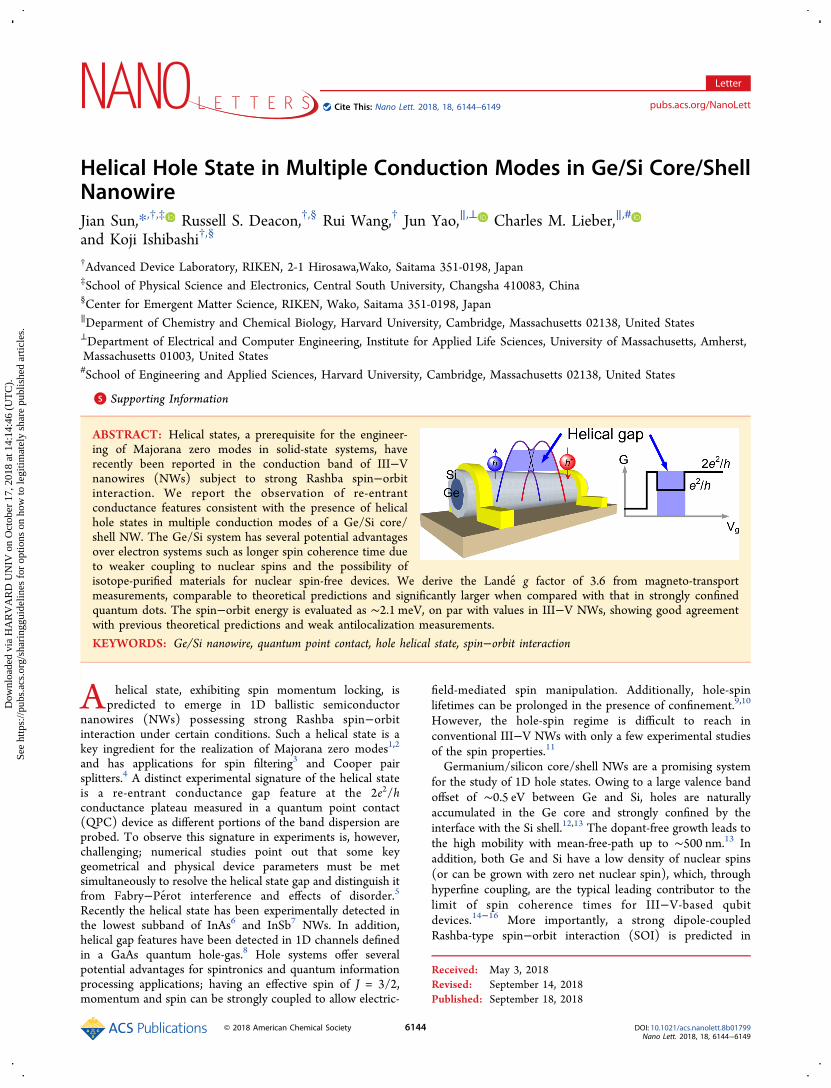
ABSTRACT: Helical states, a prerequisite for the engineer-ing of Majorana zero modes in solid-state systems, haverecently been reported in the conduction band of III−Vnanowires (NWs) subject to strong Rashba spin−orbitinteraction. We report the observation of re-entrantconductance features consistent with the presence of helicalhole states in multiple conduction modes of a Ge/Si core/shell NW. The Ge/Si system has several potential advantagesover electron systems such as longer spin coherence time dueto weaker coupling to nuclear spins and the possibility ofisotope-purified materials for nuclear spin-free devices. We derive the Lande g factor of 3.6 from magneto-transportmeasurements, comparable to theoretical predictions and significantly larger when compared with that in strongly confinedquantum dots. The spin−orbit energy is evaluated as ∼2.1 meV, on par with values in III−V NWs, showing good agreementwith previous theoretical predictions and weak antilocalization measurements.
KEYWORDS: Ge/Si nanowire, quantum point contact, hole helical state, spin−orbit interaction
A helical state, exhibiting spin momentum locking, ispredicted to emerge in 1D ballistic semiconductor
nanowires (NWs) possessing strong Rashba spin−orbitinteraction under certain conditions. Such a helical state is akey ingredient for the realization of Majorana zero modes1,2
and has applications for spin filtering3 and Cooper pairsplitters.4 A distinct experimental signature of the helical stateis a re-entrant conductance gap feature at the 2e2/hconductance plateau measured in a quantum point contact(QPC) device as different portions of the band dispersion areprobed. To observe this signature in experiments is, however,challenging; numerical studies point out that some keygeometrical and physical device parameters must be metsimultaneously to resolve the helical state gap and distinguish itfrom Fabry−Perot interference and effects of disorder.5
Recently the helical state has been experimentally detected inthe lowest subband of InAs6 and InSb7 NWs. In addition,helical gap features have been detected in 1D channels definedin a GaAs quantum hole-gas.8 Hole systems offer severalpotential advantages for spintronics and quantum informationprocessing applications; having an effective spin of J = 3/2,momentum and spin can be strongly coupled to allow electric-
field-mediated spin manipulation. Additionally, hole-spinlifetimes can be prolonged in the presence of confinement.9,10
However, the hole-spin regime is difficult to reach inconventional III−V NWs with only a few experimental studiesof the spin properties.11
Germanium/silicon core/shell NWs are a promising systemfor the study of 1D hole states. Owing to a large valence bandoffset of ∼0.5 eV between Ge and Si, holes are naturallyaccumulated in the Ge core and strongly confined by theinterface with the Si shell.12,13 The dopant-free growth leads tothe high mobility with mean-free-path up to ∼500 nm.13 Inaddition, both Ge and Si have a low density of nuclear spins(or can be grown with zero net nuclear spin), which, throughhyperfine coupling, are the typical leading contributor to thelimit of spin coherence times for III−V-based qubitdevices.14−16 More importantly, a strong dipole-coupledRashba-type spin−orbit interaction (SOI) is predicted in
Received: May 3, 2018Revised: September 14, 2018Published: September 18, 2018
Letter
pubs.acs.org/NanoLettCite This: Nano Lett. 2018, 18, 6144−6149
© 2018 American Chemical Society 6144 DOI: 10.1021/acs.nanolett.8b01799Nano Lett. 2018, 18, 6144−6149
Dow
nloa
ded
via
HA
RV
AR
D U
NIV
on
Oct
ober
17,
201
8 at
14:
14:4
6 (U
TC
).
See
http
s://p
ubs.
acs.
org/
shar
ingg
uide
lines
for
opt
ions
on
how
to le
gitim
atel
y sh
are
publ
ishe
d ar
ticle
s.
Ge/Si NWs as a result of the quasi-degeneracy in its low-energy valence bands;17 as such, Ge/Si core/shell NWs are apromising material system to investigate helical hole states.However, considering its relatively low Lande g factor, todetect the helical gap in Ge/Si NW is technically challenging.Here we report the evidence of helical hole states in a QPC
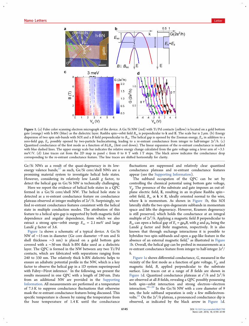
formed in a Ge/Si core/shell NW. The helical hole state isdetected as a re-entrant conductance feature on conductanceplateaus observed at integer multiples of 2e2/h. Surprisingly, wefind re-entrant conductance features consistent with the helicalstate in multiple conduction modes. The attribution of thisfeature to a helical spin-gap is supported by both magnetic fielddependence and angular dependence, from which we alsoextract a strong spin−orbit energy Eso = 2.1 meV and largeLande g factor of 3.6.Figure 1a shows a schematic of a typical device. A Ge/Si
NW of ∼15 nm in diameter (Ge core diameter ∼9 nm and Sishell thickness ∼3 nm) is placed on a gold bottom gatecovered with a ∼30 nm thick h-BN flake used as a dielectriclayer. The QPC is formed in the NW between any two Ti/Pdcontacts, which are fabricated with separations ranging from240 to 330 nm. The relatively thick h-BN dielectric helps toensure an adiabatic potential profile in the NW, which is a keyfactor to observe the helical gap in a 1D system superimposedwith Fabry−Perot inference.5 In the following, we present theresults measured in one QPC with a length of 280 nm. Datafrom an additional NW are provided in the SupportingInformation. All measurements are performed at a temperatureof 7.5 K to suppress conductance fluctuations that otherwisemask the re-entrant conductance features being discussed. Thisspecific temperature is chosen by raising the temperature fromthe base temperature of 1.4 K until the conductance
fluctuations are suppressed and relatively clear quantizedconductance plateaus and re-entrant conductance featuresappear (see the Supporting Information).The subband occupation of the QPC can be set by
controlling the chemical potential using bottom gate voltage,Vg. The presence of the substrate and gate imposes an out-of-plane electric field, E, resulting in an in-plane Rashba spin−orbit field, Bso ∝ k × E, ideally oriented normal to the wire,where k is momentum. As shown in Figure 1b, this SOIlaterally shifts the two spin-degenerate subbands in momentumspace and lifts the degeneracy. However, Kramers degeneracyis still preserved, which holds the conductance at an integralmultiple of 2e2/h. Applying a magnetic field B perpendicular toBso can open a helical gap of Ez = gμBB, with g and μB being theLande g factor and Bohr magneton, respectively. It is alsoknown that through exchange interactions it is possible tohybridize two spin subbands and open a gap-like feature in theabsence of an external magnetic field,6 as illustrated in Figure1b. Overall, the helical gap can be probed in measurements as are-entrant conductance feature from integer to half-integer 2e2/h.Figure 1c shows differential conductance, G, measured in the
vicinity of the first mode as a function of gate voltage, Vg, andmagnetic field, B, applied perpendicular to the substratesurface. Line traces cut at a range of B fields are shown inFigure 1d. Quantized conductance plateaus at e2/h and 2e2/hare observed at all B fields, revealing a QPC possibly possessingboth spin−orbit interaction and strong electron−electroninteraction.18−20 In the Ge/Si NW with a core diameter of 9nm, the hole subband separation is only a few millielectron-volts.21 On the 2e2/h plateau, a pronounced conductance dip isobserved, as indicated by the black arrow in Figure 1d.
Figure 1. (a) False color scanning electron micrograph of the device. A Ge/Si NW (red) with Ti/Pd contacts (yellow) is located on a gold bottomgate (orange) with h-BN (blue) as the dielectric layer. Rashba spin−orbit field Bso is perpendicular to k and E. The scale bar is 2 μm. (b) Energydispersion of two spin sub-bands with SOI and a B field perpendicular to Bso. The helical gap is opened by the Zeeman energy, Ez, in addition to azero-field gap, Es, possibly opened by two-particle backscattering, leading to a re-entrant conductance from integer to half-integer 2e2/h. (c)Quantized conductance of the first mode as a function of B⊥Bso (first cool down). The linear expansion of the re-entrant conductance is markedwith blue dashed lines. The upper energy scale bar indicates the relative energy change calculated from the gate voltage using a lever arm of ∼3.3meV/V. (d) Line traces cut from the 2D map in panel c from 0 to 8 T with 1 T steps. The black arrow indicates the conductance dropcorresponding to the re-entrant conductance feature. The line traces are shifted horizontally for clarity.
Nano Letters Letter
DOI: 10.1021/acs.nanolett.8b01799Nano Lett. 2018, 18, 6144−6149
6145

Importantly, it expands linearly with increasing magnetic field,as expected for the re-entrant conductance feature correspond-ing to the helical gap. Some weak conductance oscillations arenoticed. We identify them as Fabry−Perot oscillations or otherconductance fluctations, which can be distinguished from there-entrant conductance feature because they possess negligiblemagnetic response appearing as vertical “strip” features inFigure 1c. We note that the re-entrant conductance remains atB = 0 T, indicating a zero-field gap of Es. A similarphenomenon has been reported previously by Heedt et al.and Pedder et al.,6,22 in which the feature was referred to as a“pseudo-gap” introduced by the emergence of correlated two-particle backscattering and Rashba SOI. However, the featureremains under debate and can be similar in appearance to theresonance-type conductance dip induced by two-particleelectron scattering in a Rashba NW or even the presence ofan impurity state lying just below the band.23,24 Furthermore,the re-entrant conductance does not actually return to e2/h, as
may be expected if we consider a more realistic picture, withsuperimposed Fabry−Perot oscillations, inevitable disorder,possible tunneling through the gap regime, and the relativelyhigh temperature of the measurement.5
Quantized conductance plateaus and the re-entrant con-ductance can be observed in the voltage bias spectroscopy, asshown in Figure 2. Changing B field from 0 to 8 T enhancesthe energy of the helical gap from the zero-field gap of 1.51 to3.14 meV as a result of the increasing Ez, indicating a g factor of∼3.5. A diamond corresponding to the e2/h plateau is alsoobserved at zero field, which is consistent with the datapresented in Figure 1d. From Figure 2, we estimate the gatelever arm to be ∼3.3 meV/V; therefore, a comparable g factorof ∼3.6 and a zero-field gap Es ≈ 1.5 meV can also be evaluatedfrom the magneto-transport measurements plotted in Figure1c. Our evaluated g factor is larger than previously reportedvalues of g ≈ 2 found in strongly confined quantum dots25−27
Figure 2. Differential conductance, G, measured as a function of Vg and Vsd in perpendicular fields, B, of 0, 2, 4.5, and 8 T (from left to right, firstcool down). Dashed diamonds are a guide to the eye, indicating the conductance plateaus. The blue dashed lines indicate the perimeter of thehelical gap region. The red dashed lines indicate the perimeter of the e2/h plateau at zero field. Black arrows indicate the helical gap energy spacing.The horizontal dashes are provided to help to identify the development of helical gap.
Figure 3. (a) Energy dispersion of the second subband with SOI at a B field tilted by an angle θ to Bso. The helical gap size is given by Es + Ez·sin θ.The two subbands are Zeeman split by an additional energy of Ez·cos θ, resulting in the half-integer 2e2/h conductance. Note, as a simplifiedschematic, the more complex picture, for example, avoided level crossing due to the hybridization of subbands, is not presented. (b) Quantizedconductance in the second mode as a function of perpendicular B field (second cool down). Blue dashed lines highlight the linear expansion of there-entrant conductance feature. The upper energy scale bar indicates the relative energy change calculated with a lever arm of ∼1.4 meV/V. (c)Quantized conductance at B = 6 T as a function of tilt angle θ to Bso. The evolution of the re-entrant conductance feature is highlighted using theblue dashed lines. (d) Line traces cut from the 2D map in panel c at various angles. They are shifted horizontally for clarity. (e) Helical gap energy(gray dots) extracted from panel c. Red solid line is the fit using E = Es + Ez·|sin(θ + θ0)|.
Nano Letters Letter
DOI: 10.1021/acs.nanolett.8b01799Nano Lett. 2018, 18, 6144−6149
6146

but is in good agreement with the theoretical prediction for theGe/Si NW in weak electric field of ∼1 V/μm.28
The strength of the SOI Eso is roughly given by the energydifference between the bottom of the subband to the center ofthe helical gap at zero B field, as indicated in Figure 1b. Wecalculate its value as ∼2.1 meV, corresponding to a spin−orbitlength = ℏ * ≈l E m/ 2os so 7.9 nm with m* = 0.28m0. Theeffective mass of the heavy hole is used because it ispredominant in the low-energy regime in the Ge/Si NW.13
This result is consistent with an estimate of Eso = 1.5 to 3 meV,evaluated in our previous weak antilocalization measure-ments.29 The Rashba coefficient is, therefore, calculated as
α = ℏ *E m2 /so ≈ 0.34 eVÅ.An important test of the helical gap opened can be
performed by considering the angular B-field dependence.The Hamiltonian for the Rashba SOI is given as HR = (α/ℏ)(z× k)·σ, where z is a unit vector along electric field, E, and σ isthe vector of Pauli spin matrices.30 Accordingly, rotating B toBso (θ from 90 to 0°) closes the helical gap sinusoidally whilekeeping the zero-field gap, Es, untouched (Figure 3a).Magnetic-field-induced opening of the helical gap is governedonly by the B component perpendicular to Bso as Ez·sin θ.When B is aligned with Bso, the spin mixing vanishes, and weexpect a quenched helical gap. Additionally, when rotating B,two subbands are Zeeman split by an additional energy of Ez·cos θ.7 This angle dependency is a unique feature of the SOIand can be used to confirm its origin for the re-entrantconductance feature.Nevertheless, in reality, the NW inevitably hosts charged
impurities, resulting in local electric-field fluctuations com-parable to the gate-induced E, which could vary the orientationof Bso locally. In addition, to perform the angular dependencemeasurement, the fridge temperature is cycled and device isremounted. Unfortunately, after the thermal cycle, themeasurement at the first subband is found to be unstable,
with the observed gap size being inconsistent in repeated gatessweeps when in an applied magnetic field. This may be causedby the redistribution of charged impurities, resulting in thefluctuation of the orientation of Bso along the channel length.Some higher subbands, that is, second and fifth subbands,were, however, found to be stable, as the charged impurity ismostly screened, and so measurements are performed there.To verify the consistency between the helical gap predicted
by spin−orbit theory and the measured re-entrant conductancefeature, we investigate its θ dependence in the second mode.Here the device is remounted on a single axis rotator, withwhich the sample substrate can be rotated in the magnetic fieldwith the NW as the axis. Following this thermal cycle andremounting of the device, we reconfirm the presence of ahelical gap in the second mode with B-dependence measure-ments, which reveals a linear expansion of the re-entrantconductance gap with B, as indicated in Figure 3b. Using alever arm of ∼1.4 meV/V, we evaluate Ez
8T = 0.39 meV, Es =0.74 meV, and g = 0.9. Note that the enhanced carrier densityof the NW in the second mode results in a lower gate lever-armcompared with that in the first mode. Interestingly, this helicalgap is quite robust, as it is reproducible after a temperaturecycle from low to ambient temperature. Figure 3c,d indicatedthe θ dependence of quantized conductance at B of 6 Trotating from θ = 90 to 0°. As the external B field is rotatedinto the sample plane, the helical gap is decreased. We plot thehelical gap energy as a function of θ in Figure 3e. It can befitted well using the sinusoidal equation Es + Ez·|sin(θ + θ0)|,where θ0 denotes a nominal misalignment of Bso. The fittingindicates Ez
6T = 0.29 meV, Es = 0.76 meV, g = 0.9, and θ0 =6.4°, which are consistent with parameters determined fromthe B dependence in Figure 3b. Combining the results of bothB and θ dependence, we are convinced by the helical nature ofthe measured re-entrant conductance feature. The nonzero θ0implies that Bso slightly deviates from its ideal orientation (in-plane and normal to the NW axis), which can be ascribed to
Figure 4. (a) B dependence of the quantized conductance in the fifth mode measured with B oriented at various angles θ (second cool down). There-entrant conductance feature is marked with blue dashed lines. The upper energy scale bar indicates the relative energy change calculated usingthe lever arm of ∼0.6 meV/V. (b) θ dependence of the fifth mode measured at B = 5 T. The evolution of the re-entrant conductance feature isindicated by the blue dashed lines. Red dashed lines highlight the shoulder of 4.5 × 2e2/h caused by an additional Zeeman splitting of Ez·cos θ. (c)Line traces cut from panel b. They are shifted horizontally for clarity.
Nano Letters Letter
DOI: 10.1021/acs.nanolett.8b01799Nano Lett. 2018, 18, 6144−6149
6147

the geometric misalignment in sample mounting and a possiblestrong localized electric field due to defects. Considering thismisalignment and the existence of the zero-field gap, the helicalgap always persists and is never fully quenched.We now consider the device parameters, which facilitate the
clear visibility of the helical gap in our experiment. The re-entrant conductance feature associated with the helical gap canbe strongly masked by the superimposed Fabry−Perotresonances, and the helical gap may easily remain indistin-guishable in a realistic measurement. For instance, the Fabry−Perot oscillations can be observed on plateaus in Figure 1d. Toobserve the helical gap feature, the gate potential profile in theNW must be adiabatic, as discussed by Rainis and Loss.5 Theoptimal onset potential length, λ, is identified by the criticalZeeman length, λ* = 2ℏvF/(Ez + Es), with vF = α/ℏ being theFermi velocity at zero field. Then, we could calculate λ*ranging from 22 to 45 nm using these parameters extractedfrom the first mode, while the actual onset length λ isestimated as ∼33 nm using finite-element simulations(Supporting Information). We find our extracted andsimulated parameters are sufficiently close to ensure a goodvisibility of the helical gap in our measured QPC.Finally, we present measurements carried out for the fifth
conduction mode, which are consistent with the phenomenaobserved in the lower modes. Figure 4a presents B depend-ence, with B fixed at varied orientations. Figure 4b,c displaysthe θ dependence with B of 5 T and traces extracted from cutsat different θ, respectively. In both panels, the well-defined re-entrant conductance feature is observed and evolves asanticipated with B and θ. At high-index modes, electron−electron interaction strength is comparatively weaker due tothe larger hole density, leading to a vanishing zero-field gap Es.Thus the helical gap can be barely seen at θ = 0°. g factor isfound to be 0.6 from both B dependence and θ dependence,respectively. We observe a reduced g factor in higherconduction modes. This is possibly attributed to a largereffective mass in the higher modes or the enhanced electricfield, which is predicted to tune the g factor in Ge/Si NWs.28
By investigating the re-entrant conductance feature emerg-ing at quantized conductance plateaus, we detect the signatureof a helical gap for multiple conduction modes in a Ge/Si NWQPC. A Lande g factor of 3.6 and spin−orbit energy of 2.1meV are extracted for the first conduction mode, showing goodagreement with previous theoretical predictions.17,28 In view ofsuch a strong spin−orbit interaction, together with the absenceof nuclear spin, we envisage Ge/Si core/shell NWs as apromising material platform for the study of Majorana physics.Experimental Section. Device Fabrication. The Ge/Si core/
shell NW used in this work is epitaxially synthesized by a two-step vapor−liquid−solid method that has been describedelsewhere.31 First, a commercial available h-BN flake(Momentive, Polarthem grade PT11032) of ∼30 nm thicknesswas dry-transferred onto a predefined gold gate on a SiO2/Sisubstrate using a homemade mechanical manipulator with aviscoelastic membrane (Gelfilm, Gelpak).33 Then, the NW wastransferred onto the h-BN using a PMMA stamping techniquedescribed in detail elsewhere.34 Finally, electrical contacts weredefined from Ti/Pd (0.5 nm/80 nm) using e-beam lithographand evaporation. Before evaporation, a short dip in bufferedhydrofluoric acid was carried out to strip the surface oxide ofthe NW.Electrical Measurements. Measurements were performed in a
pumped He-4 refrigerator at 7.5 K. This relatively high
temperature ensures that the impact of Fabry−Perotinterference is lowered (see the Supporting Information).Two different sample inserts are used in this work. An insertwith fixed external B field aligned perpendicular to thesubstrate surface was utilized for the measurements presentedin Figures 1 and 2 (first cool down). Data presented in Figures3 and 4 were obtained with a second sample insert (secondcool down), on which the substrate can be manually rotated inthe range 0−90° from perpendicular to parallel to the externalB field. The NW was aligned by eye to the rotation axis with anaccuracy within 10°. The device experienced a temperaturecycle when we switched the insets, leading to some changes inthe transport features, most notably a change in gate voltagesat which plateaus and pinch-off were observed. The differentialconductance, G, was measured using standard lock-intechniques with an excitation voltage of <100 μV and afrequency f = 74.7 Hz. In all data presented in thisCommunication, a background resistance, arising from contactand lead regions, has been subtracted. This backgroundresistance is determined by aligning conductance plateaus tomultiples of 2e2/h (see the Supporting Information).
■ ASSOCIATED CONTENT*S Supporting InformationThe Supporting Information is available free of charge on theACS Publications website at DOI: 10.1021/acs.nano-lett.8b01799.
Quantized conductance traces, temperature dependenceof the quantized conductance measurements, simulationof the effective QPC length, additional measurements ofbias spectroscopy, and measurements of a second device(PDF)
■ AUTHOR INFORMATIONCorresponding Author*E-mail: [email protected]. Fax: +81-48-462-4659.ORCIDJian Sun: 0000-0002-7992-8092Jun Yao: 0000-0002-5269-3190Charles M. Lieber: 0000-0002-6660-2456NotesThe authors declare no competing financial interest.
■ ACKNOWLEDGMENTSWe thank Stefan Ludwig for useful discussion and HiroshiMizuta for his support on COMSOL. This work was supportedby RIKEN SPDR Fellowship, Grant-in-Aid for YoungScientists (No. 17K14076), Grant-in-Aid for ScientificResearch (Nos. 16H02204 and 15H02015), and Grants-in-Aid for Scientific Research on Innovative Areas “Science ofhybrid quantum systems” (No. 15H05867) from Japan Societyfor the Promotion of Science.
■ REFERENCES(1) Lutchyn, R. M.; Sau, J. D.; Das Sarma, S. Phys. Rev. Lett. 2010,105 (7), 77001.(2) Oreg, Y.; Refael, G.; von Oppen, F. Phys. Rev. Lett. 2010, 105(17), 177002.(3) Sato, K.; Loss, D.; Tserkovnyak, Y. Phys. Rev. Lett. 2010, 105(22), 226401.(4) Shekhter, R. I.; Entin-Wohlman, O.; Jonson, M.; Aharony, A.Phys. Rev. Lett. 2016, 116 (21), 217001.
Nano Letters Letter
DOI: 10.1021/acs.nanolett.8b01799Nano Lett. 2018, 18, 6144−6149
6148

(5) Rainis, D.; Loss, D. Phys. Rev. B: Condens. Matter Mater. Phys.2014, 90 (23), 235415.(6) Heedt, S.; Traverso Ziani, N.; Crepin, F.; Prost, W.;Trellenkamp, S.; Schubert, J.; Grutzmacher, D.; Trauzettel, B.;SchaPers, T. Nat. Phys. 2017, 13 (6), 563.(7) Kammhuber, J.; Cassidy, M. C.; Pei, F.; Nowak, M. P.; Vuik, A.;Gul, O.; Car, D.; Plissard, S. R.; Bakkers, E. P. a. M.; Wimmer, M.;Kouwenhoven, L. P. Nat. Commun. 2017, 8 (1), 478.(8) Quay, C. H. L.; Hughes, T. L.; Sulpizio, J. A.; Pfeiffer, L. N.;Baldwin, K. W.; West, K. W.; Goldhaber-Gordon, D.; de Picciotto, R.Nat. Phys. 2010, 6 (5), 336.(9) Fischer, J.; Loss, D. Phys. Rev. Lett. 2010, 105 (26), 266603.(10) Brunner, D.; Gerardot, B. D.; Dalgarno, P. A.; Wust, G.; Karrai,K.; Stoltz, N. G.; Petroff, P. M.; Warburton, R. J. Science 2009, 325(5936), 70−72.(11) Pribiag, V. S.; Nadj-Perge, S.; Frolov, S. M.; van den Berg, J. W.G.; van Weperen, I.; Plissard, S. R.; Bakkers, E. P. a. M.;Kouwenhoven, L. P. Nat. Nanotechnol. 2013, 8 (3), 170−174.(12) Xiang, J.; Lu, W.; Hu, Y.; Wu, Y.; Yan, H.; Lieber, C. M. Nature2006, 441 (7092), 489.(13) Lu, W.; Xiang, J.; Timko, B. P.; Wu, Y.; Lieber, C. M. Proc. Natl.Acad. Sci. U. S. A. 2005, 102 (29), 10046−10051.(14) Nowack, K. C.; Koppens, F. H. L.; Nazarov, Y. V.;Vandersypen, L. M. K. Science 2007, 318 (5855), 1430−1433.(15) Petersson, K. D.; McFaul, L. W.; Schroer, M. D.; Jung, M.;Taylor, J. M.; Houck, A. A.; Petta, J. R. Nature 2012, 490 (7420),380−383.(16) van den Berg, J. W. G.; Nadj-Perge, S.; Pribiag, V. S.; Plissard,S. R.; Bakkers, E. P. A. M.; Frolov, S. M.; Kouwenhoven, L. P. Phys.Rev. Lett. 2013, 110 (6), 66806.(17) Kloeffel, C.; Trif, M.; Loss, D. Phys. Rev. B: Condens. MatterMater. Phys. 2011, 84 (19), 195314.(18) Chuang, P.; Ho, S.-C.; Smith, L. W.; Sfigakis, F.; Pepper, M.;Chen, C.-H.; Fan, J.-C.; Griffiths, J. P.; Farrer, I.; Beere, H. E.; Jones,G. A. C.; Ritchie, D. A.; Chen, T.-M. Nat. Nanotechnol. 2015, 10 (1),35−39.(19) Debray, P.; Rahman, S. M. S.; Wan, J.; Newrock, R. S.; Cahay,M.; Ngo, A. T.; Ulloa, S. E.; Herbert, S. T.; Muhammad, M.; Johnson,M. Nat. Nanotechnol. 2009, 4, 759.(20) Gooth, J.; Schaller, V.; Wirths, S.; Schmid, H.; Borg, M.;Bologna, N.; Karg, S.; Riel, H. Appl. Phys. Lett. 2017, 110, 083105.(21) Liang, G.; Xiang, J.; Kharche, N.; Klimeck, G.; Lieber, C. M.;Lundstrom, M. Nano Lett. 2007, 7 (3), 642.(22) Pedder, C. J.; Meng, T.; Tiwari, R. P.; Schmidt, T. L. Phys. Rev.B: Condens. Matter Mater. Phys. 2016, 94 (24), 245414.(23) Khrapai, V. S.; Nagaev, K. E. Finite Difference Time Domain(FDTD) Simulations of Electromagnetic Wave Propagation Using aSpreadsheet. 2018, arXiv:1805.12385. arXiv.org e-Print archive.https://arxiv.org/abs/1805.12385 (accessed June 28, 2018).(24) Estrada Saldana, J. C.; Niquet, Y.-M.; Cleuziou, J.-P.; Lee, E. J.H.; Car, D.; Plissard, S. R.; Bakkers, E. P. A. M.; De Franceschi, S.Nano Lett. 2018, 18 (4), 2282.(25) Roddaro, S.; Fuhrer, A.; Brusheim, P.; Fasth, C.; Xu, H. Q.;Samuelson, L.; Xiang, J.; Lieber, C. M. Phys. Rev. Lett. 2008, 101 (18),186802.(26) Hu, Y.; Churchill, H. O. H.; Reilly, D. J.; Xiang, J.; Lieber, C.M.; Marcus, C. M. Nat. Nanotechnol. 2007, 2 (10), 622−625.(27) Brauns, M.; Ridderbos, J.; Li, A.; Bakkers, E. P. A. M.;Zwanenburg, F. A. Phys. Rev. B: Condens. Matter Mater. Phys. 2016, 93(12), 121408.(28) Maier, F.; Kloeffel, C.; Loss, D. Phys. Rev. B: Condens. MatterMater. Phys. 2013, 87 (16), 161305.(29) Wang, R.; Deacon, R. S.; Yao, J.; Lieber, C. M.; Ishibashi, K.Semicond. Sci. Technol. 2017, 32 (9), 094002.(30) Manchon, A.; Koo, H. C.; Nitta, J.; Duine, R. A.; Frolov, S. M.Nat. Mater. 2015, 14 (9), 871.(31) Yao, J.; Yan, H.; Das, S.; Klemic, J. F.; Ellenbogen, J. C.; Lieber,C. M. Proc. Natl. Acad. Sci. U. S. A. 2014, 111 (7), 2431−2435.
(32) Zomer, P. J.; Guimaraes, M. H. D.; Brant, J. C.; Tombros, N.;van Wees, B. Appl. Phys. Lett. 2014, 105 (1), 013101.(33) Castellanos-Gomez, A.; Buscema, M.; Molenaar, R.; Singh, V.;Janssen, L.; van der Zant, H. S. J.; Steele, G. A. 2D Mater. 2014, 1 (1),011002.(34) Wang, R.; Deacon, R. S.; Car, D.; Bakkers, E. P. a. M.; Ishibashi,K. Appl. Phys. Lett. 2016, 108 (20), 203502.
Nano Letters Letter
DOI: 10.1021/acs.nanolett.8b01799Nano Lett. 2018, 18, 6144−6149
6149