hc17.s7t1 the nios ii family of configurable soft-core ... · pdf filehc17.s7t1 the nios ii...
TRANSCRIPT
© 2005 Altera Corporation
The Nios II Family of
Configurable Soft-core Processors
James Ball
August 16, 2005

2 © 2005 Altera Corporation ®
Agenda
Nios II Introduction
– Configuring your CPU
FPGA vs. ASIC CPU Design
– Instruction Set Architecture
– CPU Micro-architecture
Nios II/f CPU Description
– Pipeline details
Nios II Embedded Systems
– Taking advantage of FPGA configurability

© 2005 Altera Corporation
Nios II Introduction
4 © 2005 Altera Corporation ®
Nios II Overview
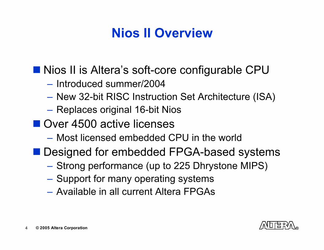
Nios II is Altera’s soft-core configurable CPU– Introduced summer/2004
– New 32-bit RISC Instruction Set Architecture (ISA)
– Replaces original 16-bit Nios
Over 4500 active licenses– Most licensed embedded CPU in the world
Designed for embedded FPGA-based systems– Strong performance (up to 225 Dhrystone MIPS)
– Support for many operating systems
– Available in all current Altera FPGAs

5 © 2005 Altera Corporation ®
Why a New Instruction Set?
Primary Issue
– Existing instruction sets optimized for ASIC
– Inefficient in FPGA
Secondary Issue
– Existing instruction sets have licensing
restrictions

6 © 2005 Altera Corporation ®
Nios II Size
Nios II
Nios II
Largest 90nm FPGA
180,000 LUTs
Smallest 90nm FPGA
4600 LUTs
13% of FPGANios II/e “economy”
1% of FPGANios II/f “fast”
FPGAFPGA
Nios II
Nios II
Nios IINios II
35¢ in lowest
cost FPGA

7 © 2005 Altera Corporation ®
Nios II is Classic RISC
32-Bit Instruction Set
32-Bit Data path
32 General-Purpose Registers
3 Instruction Formats
82 Instructions– Instruction set is not configurable
– Provides code compatibility for all implementations
Up to 256 Custom Instructions
3 Operand Instructions (2 source, 1 destination)
Optional Multiply and Divide

8 © 2005 Altera Corporation ®
PipelineController
ControlRegisters
ArithmeticLogic Unit
InterruptController
ExceptionController
General PurposeRegisters
Nios II Processor Core
Nios II Processor Block Diagram
I-Cache DebugJTAG
D-cache
Tightly-Coupled Instruction Mem
Tightly-Coupled Instruction Mem
Tightly-Coupled Data Mem
Tightly-Coupled Data Mem
clock
reset
irq[31..0]
InstructionMaster
Data Master
Custom Instructions

9 © 2005 Altera Corporation ®
Configurable Tightly Coupled Memories
Map on-chip RAMs into CPU address space
– Behave like caches that never miss
– One access every cycle without stalling
FPGA RAMs are already dual-ported
– One port for Nios II connection
– Second port available for other uses
CPU DMA
Off-chip
SDRAM
Avalon Interconnect
Tightly-Coupled Data Mem

10 © 2005 Altera Corporation ®
Configurable CPU Implementation
1200
Static
Up to 64K
no
130
5-stage
180 MHz
Nios II/s
“Standard”
600
no
no
no
30
none
210 MHz
Nios II/e
“Economy”
Size (4-input LUTs)
Branch Prediction
I-Cache
D-Cache
Max D-MIPS1
Pipeline
Nios II/f
“Fast”
1800
Dynamic
Up to 64K
Up to 64K
225
6-stage
Max Frequency1 200 MHz
1. Characteristics in Stratix II 90nm FPGA
Choose your pipeline

11 © 2005 Altera Corporation ®
Configurable Pipeline Options
Cache options
– Size
– Line size
Multiply instruction options
– Fully pipelined using built-in FPGA multipliers
– Un-pipelined using normal LUT logic
– Trap (software emulated)
Divide instruction options
– Un-pipelined using normal LUT logic
– Trap (software emulated)
12 © 2005 Altera Corporation ®
Configurable Custom Instructions
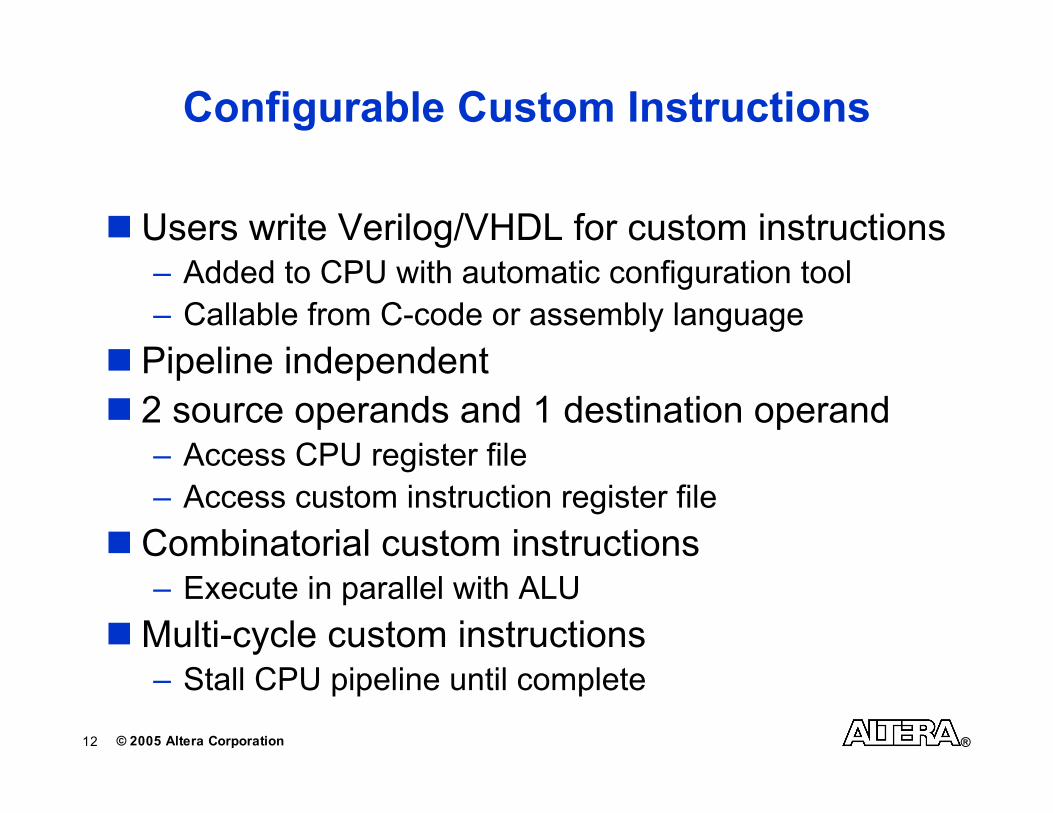
Users write Verilog/VHDL for custom instructions– Added to CPU with automatic configuration tool
– Callable from C-code or assembly language
Pipeline independent
2 source operands and 1 destination operand– Access CPU register file
– Access custom instruction register file
Combinatorial custom instructions– Execute in parallel with ALU
Multi-cycle custom instructions– Stall CPU pipeline until complete

13 © 2005 Altera Corporation ®
Configuring for Higher Performance
0
5
10
15
20
25
Mil
lio
n C
lock C
ycle
s
Software Only Custom Instruction
27TimesFaster
Example:
64 Kbyte CRC
Flash
DRAM
I/O I/O I/O
DSP
CPU
Add Custom Instructions
FPGACustom
Instruction
CPU

14 © 2005 Altera Corporation ®
Configuring for Higher Performance
Add Custom Accelerator
Flash
DRAM
I/O I/O I/O
DSP
CPUCPU
CustomAccelerator
0
5
10
15
20
25
Mil
lio
n C
lock C
ycle
s
Software
OnlyCustom
Instruction
530TimesFaster
27TimesFaster
Example:
64 Kbyte CRC
FPGACustom
Accelerator

© 2005 Altera Corporation
FPGA vs. ASIC CPU Design
16 © 2005 Altera Corporation ®
Efficient FPGA Design Guidelines
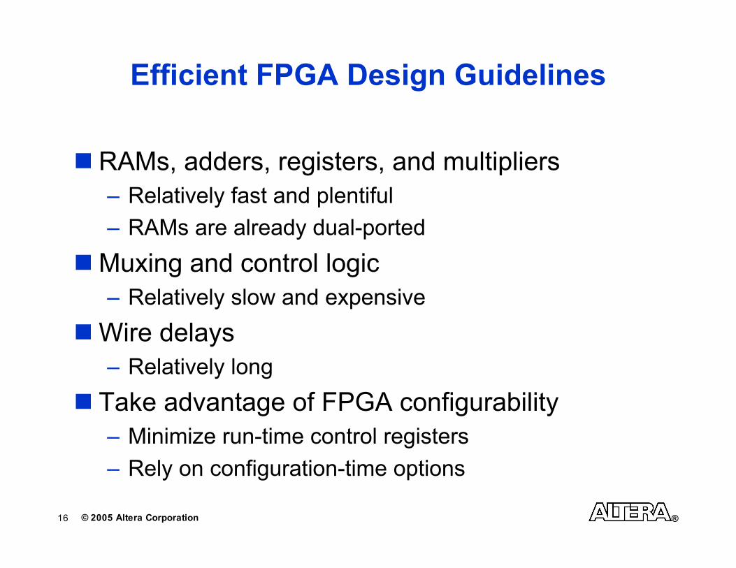
RAMs, adders, registers, and multipliers
– Relatively fast and plentiful
– RAMs are already dual-ported
Muxing and control logic
– Relatively slow and expensive
Wire delays
– Relatively long
Take advantage of FPGA configurability
– Minimize run-time control registers
– Rely on configuration-time options
17 © 2005 Altera Corporation ®
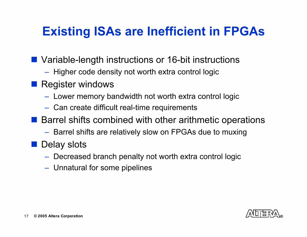
Existing ISAs are Inefficient in FPGAs
Variable-length instructions or 16-bit instructions
– Higher code density not worth extra control logic
Register windows
– Lower memory bandwidth not worth extra control logic
– Can create difficult real-time requirements
Barrel shifts combined with other arithmetic operations
– Barrel shifts are relatively slow on FPGAs due to muxing
Delay slots
– Decreased branch penalty not worth extra control logic
– Unnatural for some pipelines

18 © 2005 Altera Corporation ®
Existing ISAs are Inefficient in FPGAs
Condition code register
– Complicates pipeline control and increases muxing
Multiply/divide 64-bit operand registers
– All 64-bits rarely used in C language and increases muxing
Many run-time control registers
– Extra logic not required in a configurable FPGA CPU
Complex cache management
– State machines to initialize on reset not worth extra logic
– Many instruction options for flushing not worth extra logic
Vectored interrupts
– Not required for most designs
– Use custom instruction to reduce interrupt latency

19 © 2005 Altera Corporation ®
Getting Back to RISC Roots
CPU is an engine to run C code
– Benchmarking shows Nios II has comparable performance to
established embedded CPUs
To increase CPU performance in an FPGA
– Increase the Nios II cache size
– Add Nios II custom instructions
– Add custom accelerators
– Add multiple Nios II CPUs
– Add tightly-coupled memories
© 2005 Altera Corporation
Nios II/f CPU Description
“Fast”
21 © 2005 Altera Corporation ®
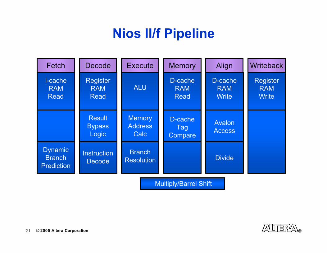
Nios II/f Pipeline
Fetch
Dynamic
Branch
Prediction
I-cache
RAM
Read
Decode
Instruction
Decode
Register
RAM
Read
Result
Bypass
Logic
Execute
ALU
Memory
Address
Calc
Branch
Resolution
Writeback
Register
RAM
Write
Multiply/Barrel Shift
Align
D-cache
RAM
Write
Divide
Avalon
Access
Memory
D-cache
RAM
Read
D-cache
Tag
Compare
22 © 2005 Altera Corporation ®
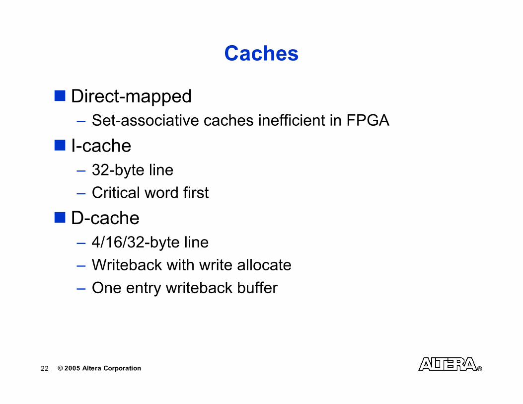
Caches
Direct-mapped
– Set-associative caches inefficient in FPGA
I-cache
– 32-byte line
– Critical word first
D-cache
– 4/16/32-byte line
– Writeback with write allocate
– One entry writeback buffer

23 © 2005 Altera Corporation ®
Dynamic Branch Prediction
2-bit branch prediction (g-Share algorithm)
– Branch History Table RAM (256x2 bits)
No Branch Target Buffer
– Simple ISA allows fast branch target calculation
Performance
– Taken branch is 2 cycles
– Not taken branch is 1 cycle
– Mispredicted branch penalty is 4 cycles
24 © 2005 Altera Corporation ®
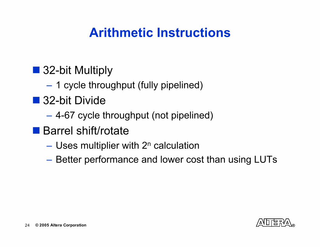
Arithmetic Instructions
32-bit Multiply
– 1 cycle throughput (fully pipelined)
32-bit Divide
– 4-67 cycle throughput (not pipelined)
Barrel shift/rotate
– Uses multiplier with 2n calculation
– Better performance and lower cost than using LUTs

© 2005 Altera Corporation
Nios II Embedded Systems
15
26 © 2005 Altera Corporation ®
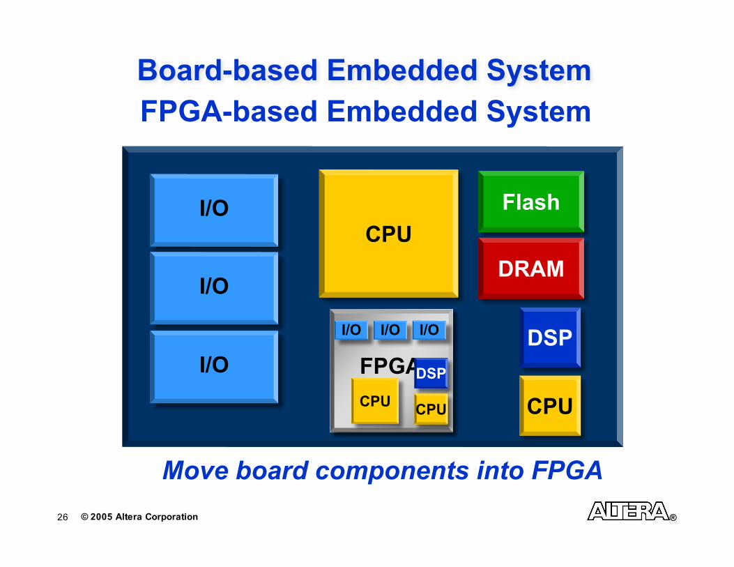
FPGA-based Embedded System
FPGA
Board-based Embedded System
Flash
DRAM
CPU
DSP
I/O
I/O
Move board components into FPGA
I/O FPGA
I/O I/O
CPU
I/O
DSP
CPU CPU

27 © 2005 Altera Corporation ®
Nios II Evaluation Board
FPGA
Flash
DRAM
2”
Preconfigured with a web
server running under µClinux

28 © 2005 Altera Corporation ®
FPGA-based Systems
It’s all configurable
– Configurable CPUs
– Configurable Memories (on-chip and off-chip)
– Configurable Peripherals
– Configurable I/O
– Configurable System Interconnect
– Custom Accelerators
and we provide the tools to make it easy …
29 © 2005 Altera Corporation ®
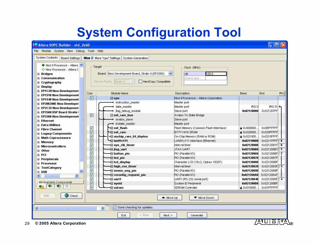
System Configuration Tool

30 © 2005 Altera Corporation ®
CPU Configuration Tool
31 © 2005 Altera Corporation ®
Avalon System Interconnect
Automatically generated for your system
Switches connect components – not a bus
Slave side arbitration
– Enables concurrent accesses
Avalon Functions
– Arbitration
– Multiplexing
– Address Decoding
– Wait-State Generation
– Dynamic Bus Sizing

32 © 2005 Altera Corporation ®
MasterArbiter
Traditional Bus Interconnect
Program
Memory
I/O
1I/O
Masters
Slaves
Processor System Bus
CPU CPUDMA
Data
Memory
Data
Memory
Program
Memory
I/O
1I/O
System
Bottleneck

33 © 2005 Altera Corporation ®
Avalon Switch Interconnect
Masters
Slaves
Avalon
CPU CPUDMA
Program
Memory
I/O
1I/O
Data
Memory
Data
Memory
Program
Memory
I/O
1I/O
Switch SwitchSwitch
Arbiter Arbiter

34 © 2005 Altera Corporation ®
Conclusions
Efficient FPGA design takes advantage of
configurable CPUs and systems
Nios II is optimized for FPGA-based systems
Established CPUs based on ISAs optimized for
ASICs are less efficient in FPGAs
© 2005 Altera Corporation
The End
Questions?
© 2005 Altera Corporation
Backup Slides

© 2005 Altera Corporation
Why a Soft-Core FPGA CPU?
20

38 © 2005 Altera Corporation ®
FPGA Soft-Core CPU Advantages
Flexibility
– Utilize existing silicon resources
Scalability
– Number of CPUs, CPU types, cache sizes, etc.
Configurability
– Generation-time configuration instead of run-time
– Eliminates logic required to control CPU options
Ubiquity
– Available in all FPGA families

39 © 2005 Altera Corporation ®
FPGA Soft-Core CPU Advantages
Relatively small compared to FPGA capacities
– Largest Altera FPGA fits 300 Nios II/e CPUs
– May have spare capacity so CPU is free
Lifecycle
– No obsolescence
– New releases of CPU improve your design
– Improved efficiency with latest silicon technologies
40 © 2005 Altera Corporation ®
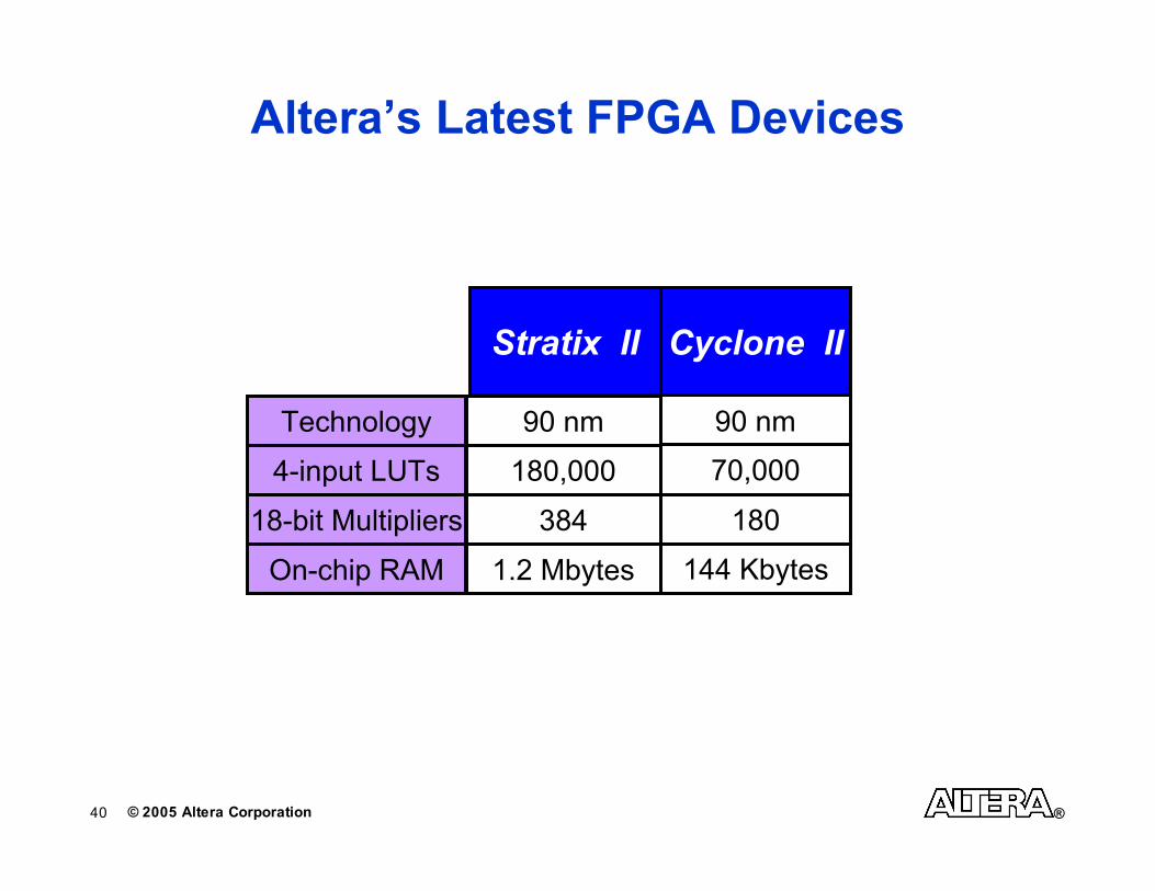
Altera’s Latest FPGA Devices
On-chip RAM
18-bit Multipliers
Technology
1.2 Mbytes
384
90 nm
4-input LUTs 180,000
Cyclone IIStratix II
144 Kbytes
180
90 nm
70,000