harmonic mixer analysis and design - stellenbosch university
TRANSCRIPT

Harm onic Mixer
Analysis and Design
Marius van der Merwe
Thesis presented in partial fulfilment of the requirements for the degree
of Master of Science (Engineering) at the University of Stellenbosch.
Promoter : Prof. JB De SwardtMarch 2002

Declaration
I, the undersigned, hereby declare that the work contained in this thesis is my own original work
and that I have not previously in its entirety or in part submitted it at any university for a degree.
Marius van der Merwe Date
Stellenbosch University http://scholar.sun.ac.za/

Summary/
Harmonic mixers are capable of extended frequency operation by mixing with a harmonic of the
LO (local oscillator) signal, eliminating the need for a high frequency, high power LO. Their
output spectra also have certain characteristics that make them ideal for a variety of applications.
The operation of the harmonic mixer is investigated, and the mixer is analyzed using an
extension of the classic mixer theory. The synthesis of harmonic mixers is also investigated, and
a design procedure is proposed for the design and realization of a variety of harmonic mixers.
This design procedure is evaluated with the design and realization of two harmonic mixers, one
in X-band and the other in S-band. Measurements suggest that the procedure is successful for the
specific applications.
Opsomming
Harmoniese mengers kan by hoer frekwensies gebruik word as gewone mengers deurdat hulle
gebruik maak van ‘n harmoniek van die LO. ‘n Hoe-frekwensie, hoe-drywing LO word dus nie
benodig nie. Die mengers se uittreespektra het ook ‘n aantal karakteristieke wat hulle goeie
kandidate maak vir ‘n verskeidenheid van toepassings. Die werking van die harmoniese menger
word ondersoek deur uit te brei op die klassieke menger-teorie. Die ontwerp van die harmoniese
menger word vervolgens ondersoek, waama ‘n ontwerpsprosedure voorgestel word vir die
ontwerp van ‘n verskeidenheid van harmoniese mengers. Hierdie prosedure word getoets met die
ontwerp en realisering van twee harmoniese mengers, een in X-band en die ander in S-band.
Vanuit die metings is dit duidelik dat die ontwerpsprosedure geslaagd is vir die spesifieke geval.
Stellenbosch University http://scholar.sun.ac.za/

Acknowledgements / Erkenning
Verskeie mense het deur die verloop van hierdie tesis verskillende bydraes gelewer. Dit is vir my
‘n voorreg om vir hulle kortliks hier dankie te se :
My studieleier, Johann de Swardt, vir sy planne, bemoediging, leiding en vertroue in my, selfs
as bladsy 6 en 7 wegraak - dis vir my ‘n konstante bron van inspirasie.
Wessel Croukamp en Ashley Cupido van SED, vir die vervaardiging van die mengers, meer
as een keer onder druk...
My vriende, vir die konstante bemoediging, kuiers, hulp en laataand sms’e.
My ouers en broer, vir hul opregte belangstelling en aanmoediging.
My verloofde, Martinette Muller, nie net vir die laat nagte se geduld en hulp nie, maar omdat
jy in my glo.
iii
Stellenbosch University http://scholar.sun.ac.za/

Contents/
List of Figures and Tables.......................................................................................................1
In troduction..................................................................................................................................5
1) Microwave Diode M ixers .................................................................................................. 8
1.1 Fundamental Mixer Theory...................................................................................................8
1.1.1 Generalized Frequency Mixing................................................................................8
1.1.2 The Diode as Nonlinear Element.............................................................................9
1.2 Diode Mixer Topologies......................................................................................................11
1.2.1 Single Diode Mixers................................................................................................11
1.2.2 Balanced Mixers......................................................................................................13
1.2.2.1 Single Balanced Mixer............................................................................14
1.2.2.2 Double Balanced Mixer...........................................................................15
1.2.2.3 Higher-Level Balanced Mixers.............................................................. 18
1.2.2.4 Subharmonic Mixers............................................................................... 18
1.3 Mixer Characteristics........................................................................................................... 20
1.3.1 Conversion Loss...................................................................................................... 21
1.3.2 Noise......................................................................................................................... 22
1.3.2.1 Inherent Noise..........................................................................................22
1.3.2.2 Signal Noise..............................................................................................23
1.3.3 Conversion Compression........................................................................................ 24
1.3.4 Intermodulation Distortion..................................................................................... 25
1.3.5 Reflection (VSWR).................................................................................................26
2) Diode Harmonic M ixers...................................................................................................30
2.1 The Schottky-Barrier Diode................................................................................................30
2.1.1 Junction Characteristics...........................................................................................31
2.1.2 Intrinsic Model........................................................................................................ 33
2.1.2.1 Large-Signal Model................................................................................. 34
2.1.2.2 Small-Signal Model................................................................................. 34
2.1.3 The Complete Diode Model................................................................................... 36
iv
Stellenbosch University http://scholar.sun.ac.za/

2.2 The Antiparallel Diode Pair.................................................................................................37
2.2.1 Single Diode Fundamentals.................................................................................... 38
2.2.2 The Antiparallel Configuration..............................................................................38
2.2.3 Two-Tone Analysis.................................................................................................41
2.2.4 IF Frequency Spectrum.......................................................................................... 43
2.3 Analysis................................................................................................................................ 44
2.3.1 Large-Signal Analysis.............................................................................................45
2.3.2 Harmonic Balance for Single Diode.......................................................................46
2.3.3 Harmonic Balance for Antiparallel Diode Pair.....................................................50
2.3.3.1 Multiport N etwork................................................................................... 51
2.3.3.2 Equivalent Diode..................................................................................... 53
2.4 Small-Signal Diode Parameters...........................................................................................55
2.4.1 Conversion Matrix for Junction Conductance....................................................... 55
2.4.2 Conversion Matrix for Junction Capacitance........................................................ 56
2.4.3 Mixer Conversion Matrix....................................................................................... 57
2.4.4 Input Impedance...................................................................................................... 60
2.4.5 Conversion Loss...................................................................................................... 61
2.5 Noise......................................................................................................................................63
2.5.1 Thermal Noise......................................................................................................... 64
2.5.2 Shot Noise................................................................................................................64
2.5.3 Noise Correlation..................................................................................................... 65
2.5.3.1 Shot Noise................................................................................................ 66
2.5.3.2 Thermal Noise..........................................................................................66
2.5.4 Signal Noise..............................................................................................................67
2.6 Diode Unbalance.................................................................................................................. 68
2.6.1 Theory....................................................................................................................... 68
2.6.2 Analysis ................................................................................................................... 69
2.7 The Antiparallel Diode Pair - A Quantitative Analysis....................................................70
2.7.1 LO Excitation...........................................................................................................70
2.7.2 Large-Signal Input Impedance............................................................................... 71
2.7.3 Model.........................................................................................................................74
v
Stellenbosch University http://scholar.sun.ac.za/

3) D esign C o n s id e ra tio n s ..................................................................................................... 76
3.1 “The Design Requirement” .................................................................................................77
3.1.1 Frequency Allocation..............................................................................................77
3.1.2 Optimum Conversion Loss..................................................................................... 78
3.1.3 Port Isolation........................................................................................................... 78
3.2 Choice of Diode....................................................................................................................79
3.3 Design Topologies................................................................................................................81
3.3.1 Series Topologies.................................................................................................... 81
3.3.1.1 Isolated Series Topology.........................................................................82
3.3.1.2 Non-Isolated Series Topology.................................................................82
3.3.2 Shunt Topology....................................................................................................... 82
3.3.3 Additional topologies..............................................................................................83
3.4 Design Overview..................................................................................................................83
3.4.1 Specifications.......................................................................................................... 84
3.4.2 Choice of Frequencies.............................................................................................84
3.4.3 Topology...................................................................................................................84
3.4.4 Choice of Diodes..................................................................................................... 84
3.4.5 Basic Design.............................................................................................................84
3.4.6 Extended Design...................................................................................................... 85
3.4.7 Simulation.................................................................................................................85
4) Im plem entation and M easu rem en ts ............................................................................. 86
4.1 S-Band M ixer....................................................................................................................... 86
4.1.1 Specifications...........................................................................................................86
4.1.2 Choice of Frequencies............................................................................................. 86
4.1.3 Topology................................................................................................................... 87
4.1.4 Choice of Diodes......................................................................................................88
4.1.5 Basic Design.............................................................................................................88
4.1.6 Extended Design.......................................................................................................90
4.1.6.1 IF Low-Pass Filter....................................................................................91
4.1.6.2 RF Band-Pass Filter..................................................................................92
4.1.6.3 IF Matching Network.............................................................................. 93
4.1.6.4 RF Matching Network............................................................................. 94
4.1.6.5 LO Isolation.............................................................................................. 95
4.1.7 Microstrip Simulation.............................................................................................. 96
vi
Stellenbosch University http://scholar.sun.ac.za/

4.1.8 Realization............................................................................................................... 99
4.1.9 Measurements........................................................................................................100
4.1.10 Comments.............................................................................................................. 102
4.2 X-Band Mixer.....................................................................................................................102
4.2.1 Specifications........................................................................................................102
4.2.2 Choice of Frequencies.......................................................................................... 103
4.2.3 Topology................................................................................................................ 103
4.2.4 Choice of Diodes...................................................................................................104
4.2.5 Basic Design.......................................................................................................... 104
4.2.6 Extended Design....................................................................................................106
4.2.6.1 IF Low-Pass Filter................................................................................. 106
4.2.6.2 RF Band-Pass Filter............................................................................... 107
4.2.6.3 IF Matching Network............................................................................108
4.2.6.4 RF Matching Network...........................................................................108
4.2.6.5 LO Isolation............................................................................................109
4.2.7 Microstrip Simulation............................................................................................111
4.2.8 Realization............................................................................................................. 113
4.2.9 Measurements........................................................................................................ 114
4.2.10 Comments...............................................................................................................115
Conclusion................................................................................................................................116
Appendix A ...............................................................................................................................119
Appendix B ...............................................................................................................................122
Appendix C ...............................................................................................................................126
References................................................................................................................................ 130
vii
Stellenbosch University http://scholar.sun.ac.za/

List of Figures and Tables/
Figure 1.1 Topology for Single Diode Mixer...............................................................................11
Figure 1.2 Frequency Spectrum of Single Diode M ixer.............................................................12
Figure 1.3 Single Balanced Mixer using a 180°-Hybrid.............................................................14
Figure 1.4 Frequency Spectrum at the IF port of typical Single Balanced Mixer.....................15
Figure 1.5 Double Balanced Mixer using three baluns...............................................................16
Figure 1.6 Typical IF Frequency Spectrum of Double Balanced Mixer................................... 17
Figure 1.7 Basic topology for Antiparallel Diode Pair Subharmonic Mixer.............................20
Figure 1.8 Typical Characteristic for Conversion Compression................................................ 25
Figure 1.9 Typical downconversion spurious response chart..................................................... 26
Figure 1.10 Output Spectrum for fRF = 8 GHz and fRF = 8.25 GHz..........................................27
Figure 1.11 Typical Diode Input Impedance for different LO power levels............................... 29
Figure 2.1 The Schottky diode junction.......................................................................................31
Figure 2.2 Intrinsic Schottky-Barrier Diode Model....................................................................34
Figure 2.3 Small- and Large-signal calculation of g(V)..............................................................35
Figure 2.4 Complete Schottky-Barrier Diode Model..................................................................36
Figure 2.5 Conductance Waveform g(t) for a single diode........................................................ 38
Figure 2.6 Antiparallel diode configuration................................................................................ 38
Figure 2.7 Junction Conductance g for Antiparallel Diode Pair................................................40
Figure 2.8 Output Spectrum of Antiparallel Diode Pair..............................................................43
Figure 2.9 LO Noise Rejection in Antiparallel Diode Pair........................................................ 44
Figure 2.10 Diagram of Generalized Mixer Analysis...................................................................45
Figure 2.11 Equivalent Circuit of Mixer with Single Diode........................................................ 47
Figure 2.12 Division of diode circuit in Linear and Nonlinear parts........................................... 48
Figure 2.13 Large-Signal circuit of a mixer with an antiparallel diode pair.............................. 51
Figure 2.14 Equivalent circuit of Antiparallel diode pair driven by LO .....................................54
Figure 2.15 Equivalent Mixer Circuits at harmonics of the LO...................................................54
Figure 2.16 Small-Signal equivalent model for mixer with antiparallel diode pair...................58
Figure 2.17 Alternative Small-signal representation of Diode Mixer......................................... 63
Figure 2.18 Adaptation of the Schottky Diode model to include the effects of shot noise and
thermal noise...............................................................................................................65
Stellenbosch University http://scholar.sun.ac.za/

Figure 2.19 Antiparallel diode pair LO time-Waveform..............................................................70
Figure 2.20 Spectrum of Antiparallel Diode Pair LO Waveform............................................... 70
Figure 2.21 Antiparallel Diode Pair Capacitance modulated by LO...........................................71
Figure 2.22 Antiparallel Diode Pair Conductance modulated by L O .........................................71
Figure 2.23 Input Impedance of Antiparallel Diode Pair as function of LO Power...................72
Figure 2.24 Input Impedance of Single Diode as function of LO power....................................72
Figure 2.25 Junction Capacitance as a function of Junction Voltage Vj for single diode and the
Antiparallel diode pair................................................................................................72
Figure 2.26 Input Impedance of the Antiparallel Diode Pair for swept LO Power at 5 GHz ...73
Figure 2.27 Real part of the Antiparallel Diode Pair Junction Impedance..................................73
Figure 2.28 Imaginary part of the Antiparallel Diode Pair Junction Impedance........................ 73
Figure 2.29 Simulated Reflection Coefficient for the HSMS-8202 diode pair...........................74
Figure 2.30 Final Model for HSMS-8202 Antiparallel Diode Pair............................................. 75
Figure 3.1 IF Output Power for variation in Junction Capacitance........................................... 80
Figure 3.2 IF Output Power for variation in Series Resistance..................................................80
Figure 3.3 IF Output Power for variation in Diode Non-Ideality.............................................. 80
Figure 3.4 IF Output Power for variation in Series Inductance..................................................80
Figure 3.5 Isolated Series Topology.............................................................................................81
Figure 3.6 Non-Isolated Series Topology.................................................................................... 81
Figure 3.7 Shunt Topology............................................................................................................83
Figure 4.1 Intended topology for S-band 2nd harmonic mixer..................................................87
Figure 4.2 MWO layout of the Basic Design.............................................................................. 89
Figure 4.3 Impedance on the Small-Signal port.......................................................................... 89
Figure 4.4 Output Spectrum of the Small-Signal Port.................................................................90
Figure 4.5 Intended Topology showing Matching Circuits and Filters..................................... 91
Figure 4.6 Low-Pass Filter Frequency Response........................................................................ 92
Figure 4.7 Band-Pass Filter Frequency Response for realized microstrip filter.......................92
Figure 4.8 RF port Input Impedance............................................................................................ 93
Figure 4.9 IF port Input Impedance.............................................................................................. 93
Figure 4.10 RF port Input Impedance (after the addition of the IF matching network).............94
Figure 4.11 IF port Input Impedance (after the addition of the IF matching network)..............94
Figure 4.12 Final RF port Input Impedance (after the addition of the IF and RF matching
networks)..................................................................................................................... 95
2
Stellenbosch University http://scholar.sun.ac.za/

Figure 4.13 Final IF port Input Impedance (after the addition of the IF and RF matching
networks).................................................................................................................... 95
Figure 4.14 Frequency Spectrum at LO port (before isolation)..................................................96
Figure 4.15 Frequency Response of implemented LO LPF........................................................96
Figure 4.16 Simulated IF power as a function of LO power for the S-band Harmonic Mixer .97
Figure 4.17 Simulated Output Spectrum at the IF Port............................................................... 98
Figure 4.18 Simulated plot of RF frequency vs IF power........................................................... 98
Figure 4.19 Final S-band mixer layout......................................................................................... 99
Figure 4.20 The Manufactured S-band Harmonic Mixer.......................................................... 100
Figure 4.21 Measured LO power vs IF power for S-band harmonic mixer........................... 101
Figure 4.22 Measured RF-sweep for S-band harmonic mixer showing IF amplitude against IF
frequency...................................................................................................................101
Figure 4.23 Measured LO power vs IF power for X-band harmonic m ixer............................103
Figure 4.24 Input Impedance on the Small-Signal port............................................................. 105
Figure 4.25 Small-Signal Port Output Spectrum........................................................................105
Figure 4.26 Low-Pass Filter Frequency Response.....................................................................107
Figure 4.27 Band-Pass Filter Frequency Response for realized microstrip filter................... 107
Figure 4.28 IF port Input Impedance (after the addition of the IF matching network)...........108
Figure 4.29 RF port Input Impedance (after the addition of the IF matching network)......... 108
Figure 4.30 Final RF port Input Impedance (after the addition of the IF and RF matching
networks)...................................................................................................................109
Figure 4.31 Final IF port Input Impedance (after the addition of the IF and RF matching
networks)...................................................................................................................109
Figure 4.32 Frequency Spectrum at LO port (before isolation)................................................110
Figure 4.33 Frequency Response of implemented LO BPF...................................................... 110
Figure 4.34 Simulated LO power against IF Power of the X-band Harmonic M ixer.............111
Figure 4.35 Simulated Output Spectrum at the IF Port............................................................. 112
Figure 4.36 Simulated plot of RF frequency against IF power for the X-band m ixer............112
Figure 4.37 Layout of finalized X-band mixer........................................................................... 113
Figure 4.38 The Manufactured X-band Mixer........................................................................... 113
Figure 4.39 Measured LO power vs IF power for X-band harmonic m ixer............................114
Figure 4.40 Measured RF-sweep of X-band harmonic mixer...................................................115
3
Stellenbosch University http://scholar.sun.ac.za/

Figure A.l Large-Signal Circuit used for the Reflection Algorithm.........................................119
Figure A.2 The division of the mixer circuit into equivalent circuits for use with the
Reflection Algorithm.............................................................................................. 120
Figure B.l S-Band Harmonic Mixer Layout.............................................................................. 122
Figure B.2 Lumped Topology for the IF low-pass filter........................................................... 123
Figure B.3 Response for the IF low-pass filter.......................................................................... 123
Figure B.4 Microstrip Topology for LO low-pass filter............................................................124
Figure B.5 Response for the LO low-pass filter......................................................................... 124
Figure B.6 Microstrip Topology for RF band-pass filter.......................................................... 125
Figure B.7 Response for the RF low-pass filter......................................................................... 125
Figure C. 1 X-Band Harmonic Mixer Layout............................................................................. 126
Figure C.2 Topology for the IF low-pass filter.......................................................................... 127
Figure C.3 Response for the IF low-pass filter.......................................................................... 127
Figure C.4 Microstrip Topology for LO band-pass filter.......................................................... 128
Figure C.5 Response for the LO low-pass filter......................................................................... 128
Figure C.6 Microstrip Topology for RF band-pass filter.......................................................... 129
Figure C.7 Response for the RF band-pass filter....................................................................... 129
Table 1.1 Summary of Characteristics for Single Diode Mixer................................................13
Table 1.2 Summary of Characteristics for Single Balanced Mixer...........................................15
Table 1.3 Summary of Characteristics for Double Balanced Mixer.........................................17
Table 2.1 Selected Diode parameters for HSMS-820x-series................................................... 37
Table 2.2 Comparison of Mixer Performance for Diode Unbalance caused by variation of
Diode Parameters....................................................................................................... 69
4
Stellenbosch University http://scholar.sun.ac.za/

Introduction
Frequency mixers are used to achieve frequency conversion of an input signal. A nonlinear
device, most commonly a diode or transistor, is used for this purpose. The nonlinear device
generates the necessary integer multiples, or harmonics, of the signals that are necessary for the
process of frequency conversion. This process can be described by the following general
equation
where cds is the input signal, cop is the signal driving the mixer, and com,n is the output signal. Here
m and n are integers denoting the harmonic of the input signal and driving signal respectively.
For conventional mixers \m\ = 1 and \n\ = 1. Conventional mixers therefore use the fundamental
frequencies of the input and driving signals to perform the frequency conversion, and are
subsequently collectively called fundamental mixers. These mixers require a driving signal (Op
with a frequency of the same order as the frequency of the input signal cos to produce an output
signal.
With the upper frequency barrier of communication systems continuously creeping upwards
(with the occasional leap), it becomes increasingly difficult to realize stable, powerful and cost
effective driving sources for the fundamental mixers. A mixer topology utilizing an easily
realizable driving source of lower frequency, while still taking a higher frequency input signal
would provide a solution to the problem.
The harmonic mixer is such a topology. Harmonic mixers, while still obeying the above
equation, require \m\ = 1 and \n\ > l . A harmonic of the lower frequency driving signal is
therefore utilized in order to produce an output signal of the same frequency as a fundamental
mixer. Apart from the ability to utilize a lower frequency driving signal, the harmonic mixer
provides the additional advantage of rejecting certain frequency components associated with
conventional mixers. The operation of diode multipliers is in some aspects very similar to that of
harmonic mixers, and it is not surprising that the multipliers incorporate similar structures as the
harmonic mixer.
5
Stellenbosch University http://scholar.sun.ac.za/

Harmonic mixers were first introduced in 1975 [1]. Initially conversion losses of 5 to 8 dB worse
than equivalent fundamental mixers were obtained [2], However, harmonic mixers have evolved
to provide very competitive conversion losses at lower frequencies, while they are an established
technology at higher frequencies [41, 42, 43]. Using 2nd-order mixers, 5 dB conversion loss at
100 GHz has been achieved [3], while lOdB loss at 230 GHz demonstrates the power of this
technology [38].
Harmonic mixers can utilize the higher order even harmonics of the driving signal, with a
corresponding increase in conversion loss. Examples include a 6th-order mixer producing 24 dB
loss at 26 GHz, a lO^-order mixer producing 28 dB loss at 50 GHz, and a lS^-order mixer
producing 46 dB loss at 110 GHz [4]. The harmonic mixer therefore provides a convenient
method of achieving acceptable conversion loss, without the need for a specialized source
producing driving signal of adequate power at high frequencies.
The purpose of this thesis was to investigate the properties and implementation possibilities of
the harmonic mixer. Its aim is to characterize the harmonic mixer adequately in terms of existing
mixer properties. The operation and performance of the harmonic mixer were to be explored by
means of design examples, and the minimization of conversion loss was chosen to be an
important design criteria. Due to its extensive nature, noise analysis was restricted to the basics.
The thesis is divided into two main parts : the first part explores the analysis of the harmonic
mixer with reference to conventional mixer theory. In many instances it is possible to extend
existing mixer theory to accommodate the harmonic mixers. The second part explores the
synthesis of the harmonic mixer, setting out to create a comprehensive design procedure which
to date is not readily available in literature. The aim was to create a design procedure which
considers the as many as possible of options offered by harmonic mixers, and then provide a
step-by-step method for realizing a variety of harmonic mixers. Such a procedure was created
and evaluated by designing two harmonic mixers. The procedure proved adequate and
repeatable, producing a mixer at X-band with a conversion loss of 7.8 dB.
Chapter 1 provides a general overview of the basic structures employed for frequency
conversion. The harmonic mixer is introduced, and an overview of its properties is given. The
chapter concludes with an overview of the general properties used to describe mixer operation.
6
Stellenbosch University http://scholar.sun.ac.za/

Chapter 2 is a detailed description of the diode harmonic mixer. The operation of the diode
harmonic mixer is considered, and the antiparallel diode pair is introduced as a fundamental
building block of the harmonic mixer. The analysis of the mixer is subsequently discussed, with
emphasis on the large-signal and small-signal analysis. Conversion loss, noise and other mixer
properties are then related to the harmonic mixer. The chapter concludes with a comprehensive
discussion on the analysis, paving the way for mixer synthesis.
Chapter 3 contains a detailed discussion of the various design considerations of the harmonic
mixer. The mixer properties of Chapter 2 are related to various design methods. The chapter
concludes with a proposed design procedure for harmonic mixers.
Chapter 4 contains two implementations of the design procedure proposed in Chapter 3. Both S-
band and X-band harmonic mixers are designed and realized, and their performance is discussed.
This discussion is carried over to the Conclusion, where a few final ideas are presented.
The Appendix contains discussions and design procedures omitted from the text.
7
Stellenbosch University http://scholar.sun.ac.za/
Chapter 1 : Microwave Diode Mixers
Out of all the different mixer classes, diode mixers are the most versatile tool to perform
frequency conversion. Although they have been around since 1939, the simplicity and yet
versatility have preserved their usefulness. In the mm-wave region and beyond, they are still
utilized almost exclusively due to the limitations of active devices. In the RF and microwave
region they constantly compete with newer technology, and are still often preferred to more
complex circuits.
This chapter will investigate the usefulness of the diode mixer in the microwave region. It starts
with a mathematical description of the process of frequency conversion, or mixing. Thereafter
the diode is introduced as a nonlinear element capable of performing frequency conversion.
Once the role of the diode as a tool for frequency conversion has been defined, its application in
standard mixer circuits and topologies for the microwave region is investigated. The harmonic
mixer is introduced, and the basics of operation are considered. The chapter is concluded with a
discussion of the terminology and properties used to characterize mixers.
1.1) F undam enta l Mixer Theory
Frequency conversion, or mixing, is achieved when a periodic signal of frequency ras is
modulated by a periodic conductance waveform with frequency rap. The periodic signal is called
the RF signal {radio frequency), while the periodic conductance is a result of an applied LO
signal (local oscillator). The current resulting from the RF signal being modulated by the LO
signal contains the generated frequency products, otherwise known as the sum and difference
products.
1.1.1 Generalized Frequency Mixing
A frequency mixer is essentially a multiplier. Any nonlinear device can be used to perform the
frequency mixing, as will be demonstrated. A voltage v (the independent variable) is applied
across such an element with a nonlinear transfer function, with the current z'd (the dependent
variable) flowing through the element as a result of the applied voltage.
8
Stellenbosch University http://scholar.sun.ac.za/

This current-voltage, or I-V, characteristic of the nonlinear device can be described by a power
series of the form
id = a0 + axv + a2v2 + a 3v3 + ... ............... (1.1)
where ao, ai, ci2, ... are suitable coefficients [5]. Equation (1.1) summarizes the general relation
for the currents and voltages associated with a nonlinear device.
1.1.2 The Diode as Nonlinear Element
The I-V relationship of the general diode provides the required mechanism for frequency
conversion. The diode is not the only nonlinear element exhibiting this relationship - the I-V
curves of various families of transistors also obey the relationship in equation (1.1), and they are
consequently employed as frequency mixers.
In general there will be two voltages applied across the nonlinear diode :
1) The periodic RF signal vs, which is generally of the form
v,(0 = K cos{cost)
2) The periodic LO signal vp, which is generally of the form
vp(t) = Vp cos(copt)
The phase angles cos and cop of the RF and LO signal respectively are ignored for the purpose of
this qualitative discussion. When these two signals are applied across a diode simultaneously, the
nonlinear current z'd from equation (1.1) flowing in the diode as a result of the applied voltages is
given by
h (0 = K (0 + h (0 + K (0 + • • • ..................... ( 1 -2 )
The general trigonometric identities were used to obtain
9UNIVERSITEiT STELLENBOSCH
BIBLIOTEFK
Stellenbosch University http://scholar.sun.ac.za/

ia( 0 = ia(t) = aVs cos(a>st)+aVp cos(o)pt) ............... (1.3)
ib (0 = \b [ V] + V] + Vs2 cos(2<y/)+ Vs2 cos(2<opt)
+ 2VsVp{cos((®, + cop)/)+ cos((<y, - © , ) } ] (1.4)
ic (0 = tcI eos(3ffl,r) + Fp3 cos(3cy)
+ 3K/KJ,{cos((2®f + a ,)r)+ cos
+ 3 r ,^ 2{cos((2ffl, +ffl,y)+ COS ((2 0 ,-« ,) /) (
+ 3(F,! + 2 r / pJ)cos(®,/)
+ 3(r;+2F ,2F,,)cos(®,f)] (1.5)
where a, c, ...are general coefficients. What is important to note, is that frequencies other than
all the generated frequency products are a linear combination of the two excitation frequencies,
or
where m,n = ..., -2, -I, 0, +1, +2, ... The fundamental mixing product with m - 1 and n = -1 is
in most cases the desired intermediate frequency, or IF, while the second order mixing product
with m = -1 and n = 2 is termed the image. The order of the mixing product is given by \m\.
Mixing products with orders greater than one are called intermodulation products, IM products
or spurs [6, 37].
Although not formally, the output spectrum of the mixer provides an additional means of
characterization for the different types of frequency mixers. Apart from aspects such as physical
diode topology, conversion loss, frequency range of operation etc., a given type of mixer (e.g. a
“double balanced mixer”) always implies a certain frequency content of the output spectrum.
In mixer selection and design it is fundamental to have a knowledge of the output spectrum of a
specific frequency mixer. Standard considerations include the amount of LO power “leaking
through” to the IF, how much of the power available to the IF is lost to the image, and how the
those of the original signals are created. A closer inspection of equations (1.3) - (1.5) reveals that
(1.6)
10
Stellenbosch University http://scholar.sun.ac.za/

output filters need to be designed in order to filter out the intermodulation products. In the
following sections the classic topologies for diode frequency mixers will be considered with
reference to their output spectra.
1.2) D io d e Mixer T op olog ies
Diode frequency converters are primarily classified by the number of diodes they employ, and by
the manner in which these diodes are arranged in the circuit. The mixers can further be classified
by their frequency band of operation (e.g. X-band), the medium used for wave-propagation (e.g.
stripline), or a special function the mixer performs (e.g. image enhancement). An overview of
the most common topologies with a brief description of their operation is given.
1.2.1 Single Diode Mixers
Single diode mixers (or single-ended mixers) provide the simplest way of frequency conversion.
A single diode mixer essentially comprises a diode embedded in two matching networks : one
combined network for the LO and RF, and one network for the IF. Figure 1.1 shows the standard
topology for a single diode mixer.
Single diode mixers are rarely used at frequencies below the millimeter-wave region. Their
simplicity and minimal components make them the only truly effective mixers at higher
frequencies, but at lower frequencies they are outperformed by improved configurations. As it
might have been expected, the analysis and synthesis of single diode mixers provide the
“building blocks” for most multi-diode mixers. Multi-diode mixers can essentially be reduced to
equivalent single diode mixers [7].
11
Stellenbosch University http://scholar.sun.ac.za/

The typical frequency spectrum of the current flowing through the diode is shown below.
Although the graph only shows mixing products up to the 3 rd order, it is clear that the lower
order mixing products are generally those of interest, since the amplitude of these lower order
mixing products makes it necessary to consider them when designing input and output filter
networks. Also note the “tapering” of the amplitudes as the frequency increases; as it can be
expected, the majority of the power lies at the mixing products of the fundamental RF and LO
frequencies, while less power is available at the higher frequencies.
O A « <cv * r
o” o ' y * o* ^V Frequency
Figure 1.2 : Frequency Spectrum of Single Diode Mixer (up to 3rd order mixing products)
The frequency content of the current through the single diode mixer is typical for any general
nonlinear element. The various frequency components described by equations (1.3) - (1.5) can
be graphically identified above. Specific frequencies to note are as follows :
- The RF and LO, with their harmonics
- The IF : {-LO + RF}
- The Image Frequency : {2LO - RF}
- Even-order IM products : {-LO + RF}, {2LO + 2RF}, etc.
- Odd-order IM : {2LO - RF}, {-2LO - 3RF}, etc.
As a measure of comparison to the topologies of the following sections, it is noted that the
frequency spectrum of the current through the single diode contains the LO and RF signals, and
all their harmonics. There is consequently no inherent isolation of these signals from the IF port.
Removing these signals from the IF port is a task that must be done completely by means of
filtering. It is also noted that the spectrum contains both the even-order and odd-order IM
products. The single diode mixer therefore provides no spurious-response rejection', a task that
must once again be done entirely by filtering.
12
Stellenbosch University http://scholar.sun.ac.za/

Finally, it is noteworthy that any amplitude or phase noise present in the LO will be directly
“translated” to the IF signal - therefore there is no noise-rejection.
To conclude, single diode mixers have the following general characteristics :
Characteristic Performance
Isolation No isolation between LO, RF and IF
Spurious-response rejection No rejection of even- or odd-order IM products
Noise-rejection No rejection of LO amplitude or phase noise
Frequency Range Classic mixer for higher GHz-region
Table 1.1 : Summary of Characteristics for Single Diode Mixer
Although the single diode mixer is predominantly used in the mm-wave region and beyond,
more complex topologies generally outperform this mixer at lower frequencies. These topologies
will briefly be discussed in the following section.
1.2.2 Balanced Mixers
In addition to single diode mixers, balanced mixers provide a further dimension to frequency
conversion. Their multi-diode configurations allow for certain very attractive characteristics, as
will be shown shortly. Balanced mixers usually employ diodes in groups of 2, 4 or 8, and are
characterized accordingly. The harmonic mixer has often been characterized as a sub-division of
balanced mixers, since its operation is in some ways similar to that of a balanced mixer. The
operation of the balanced mixer will briefly be presented here in order to verify and explore this
classification of the harmonic mixer.
Apart from utilizing more than one diode, balanced mixers make use of hybrids and baluns [8].
A hybrid circuit has an isolated port, and provides a phase difference (usually 90° or 180°,
depending on the design). When the LO and RF signals are applied as unbalanced signals at the
input ports, the hybrid produces a balanced signal consisting of a combination of the LO and RF
signal on each of its output ports. A balun simply converts a balanced transmission line to an
unbalanced line. Single balanced mixers utilize one hybrid or balun, while double balanced
mixers use more than one. At lower frequencies the baluns are realized using transformers, while
distributed elements are used at GHz-frequencies.
13
Stellenbosch University http://scholar.sun.ac.za/

1.2.2.1 Single Balanced Mixer
Figure 1.3 shows the typical topology for a single balanced mixer. The circuit essentially utilizes
a 180° hybrid and two diodes. The LO voltage over the diodes is out of phase by 180°, while the
RF voltage appearing over the diodes is in phase. These phase differences are characteristic of
the specific hybrid, and they determine the harmonic content of the IF.
The method of analysis in the current text for determining the frequency content at the IF port is
qualitative, and general to all the types of balanced mixers that are presented in the following
sections [9].
For the LO : It can be shown that each diode contains frequency components at all the
harmonics of the LO. However, the pair of diodes produces no frequency components at any
of the LO harmonics. The respective diode currents at the harmonics of the LO must therefore
be equal but opposite, cancelling at the IF port.
For the RF : It can also be shown that each diode contains frequency components at all the
harmonics of the RF. The pair of diodes, however, only has frequency components at the odd
harmonics of the RF. The respective diode currents at the even harmonics of the RF must
therefore be equal but opposite in phase, cancelling at the IF port.
Although all the frequency components of the LO are confined to the loop containing the diodes
and the hybrid, the mixing products containing these components (e.g. {2LO - RF}, {LO +
3RF}) are not limited to the loop, and appear at the IF port where they can be filtered out by the
IF Filter. Figure 1.4 below shows a typical output spectrum for a single balanced mixer, with
mixing products to the 3rd order. The frequency components characteristic of the single diode
mixer that are not present (i.e. rejected) in the single balanced mixer have been grayed.
14
Stellenbosch University http://scholar.sun.ac.za/

/
Figure 1.4 : Frequency Spectrum at the IF Port of typical Single Balanced Mixer
The single balanced mixer also has the property of rejecting LO amplitude noise (or AM noise)
at IF frequencies. The noise voltage Vn that enters the mixer at the LO port, is 180° out of phase
through the diodes, and cancels at the IF port. As can be expected, the IF has much improved
isolation from the LO signal (limited mainly by the degree o f balance in the circuit, which is in
turn determined by the quality of the hybrid, and the similarity of the two diodes).
To conclude, single balanced mixers have the following general characteristics :
Characteristic Performance
Isolation Good isolation between LO and IF
No isolation between RF and IF
Spurious-response rejection (1) All {mu)s + nuip} mixing products with m and n even
are eliminated (e.g. {-2LO + 2RF})
(2) All {mcjs + ncop} mixing products with m even and n
odd are eliminated (e.g. {-LO + 2RF})
Noise-rejection Rejection of LO amplitude noise
Frequency Range MHz-range (baluns) and low GHz-range (hybrids)
Table 1.2 : Summary of Characteristics for Single Balanced Mixer
1.2.2.2 Double Balanced Mixer
A double balanced mixer typically uses four diodes and three baluns. Figure 1.5 shows a
configuration for displaying the operation of the double balanced mixer. (In practice the mixers
are rarely realized in this way. A ring- or star-configuration, described later, is often used.)
15
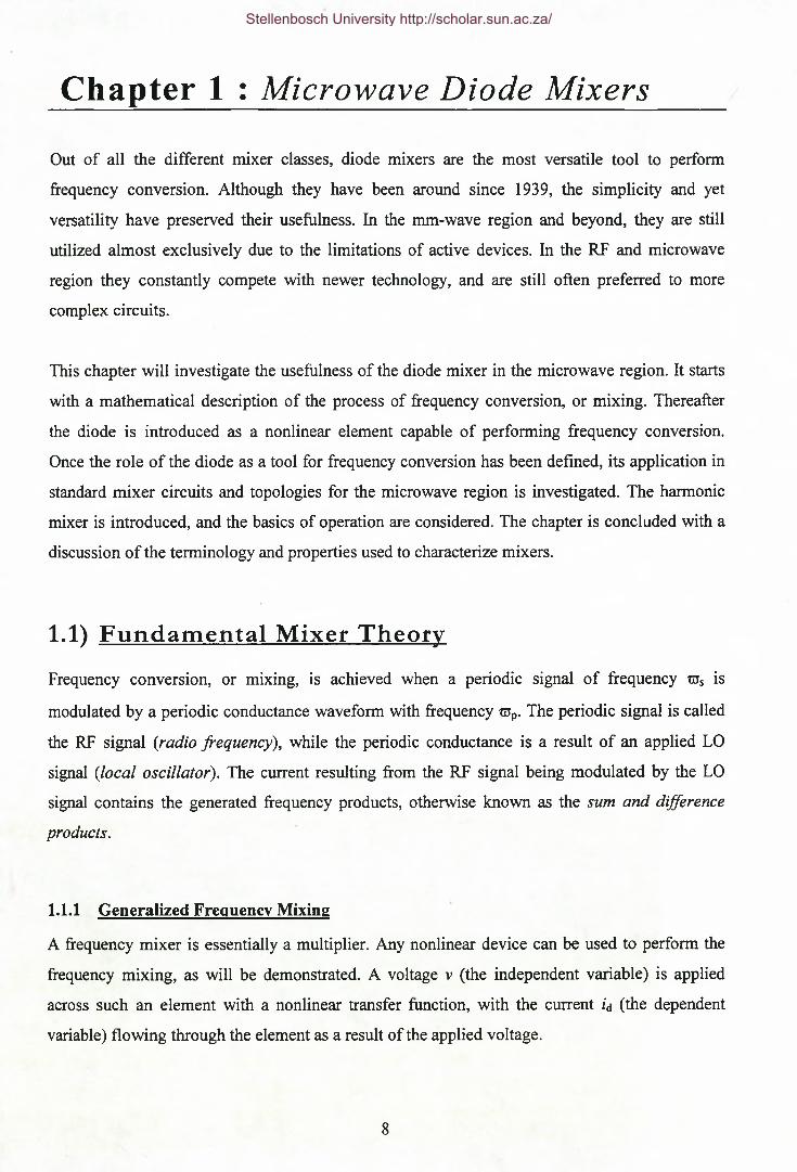
Stellenbosch University http://scholar.sun.ac.za/
Once again the analysis of the double-balanced-topology presented here will be intuitive, as a
detailed description will be given in later sections. Since the two diodes connected to the
secondary of each of the LO baluns are identical, points A and A’ are virtual grounds for the LO.
In the same way points B and B’ are virtual grounds for the RF. During the positive half of the
LO cycle, A’ is ideally connected to virtual ground, while A is ideally open. The part of the RF
balun’s secondary between A’ and the IF port is therefore connected. During the negative half of
the LO cycle the part of the RF balun’s secondary between A and the IF port is connected. As a
result of this “switching” action the RF applied to the IF port is switched at the LO frequency.
The conductance waveform due to the LO has half-wave symmetry (a result of the “switching”
action), and therefore contains no even harmonic components.
For the LO : It can be shown that all the diodes contain all the harmonics of the LO.
However, the lines from the 1-2 and 3-4 pairs of diodes (see Figure 1.5) to the secondary of
the RF balun contain no frequencies at the harmonics of the LO. Consequently, for both the 1 -
2 and 3-4 loops, the harmonic currents must be equal but opposite in phase, cancelling at both
ports of the RF secondary. Ideally the IF is completely isolated from the LO, since the RF
balun is free of any LO frequency content.
For the R F : In a situation similar to that of the single balanced mixer, the 1 -2 and 3-4 pairs
of diodes permit only current components at the odd harmonics of the RF to flow between the
diodes and the secondary of the RF balun. Since it can be shown that all diodes contain all
harmonics of the RF, the diode currents at the even harmonics of the RF must therefore be
equal but opposite in phase. The remaining odd harmonics from the 1-2 and 3-4 pairs of
diodes add in the secondary of the RF balun, and since they are of equal magnitude but
opposite phase, they too cancel in the ideal case, and the IF is completely isolated from the
RF.
16
Stellenbosch University http://scholar.sun.ac.za/

Figure 1.6 shows a typical output spectrum for a double balanced mixer (with mixing products to
the 3rd order).
Figure 1.6 : Typical IF Frequency Spectrum of Double Balanced Mixer
Because the frequency content in the secondary of the RF balun is even more limited than the
diode loop of the previously discussed single balanced mixer, the IF spectrum contains even less
mixing products. Only products of odd LO and RF harmonics are present.
Double balanced mixers are seldom realized as depicted in Figure 1.5. Slight variations of the
topology permit a double balanced mixer with improved performance. The Ring Mixer is created
by connecting both points labelled B in Figure 1.5, as well as both points labelled B’. The Star
Mixer is created by essentially extracting the IF signal from a common point connecting all four
diodes. Further discussion on their operation will be omitted from this overview.
To conclude, double balanced mixers have the following general characteristics :
Characteristic Performance
Isolation Good isolation between LO and IF
Good isolation between RF and IF
Spurious-response rejection Only {mojs + ncop) mixing products with m and n
odd are permitted (e.g. -3LO + RF)
AM Noise-rejection Rejection of LO amplitude noise (similar to single
balanced mixer)
Frequency Range Low GHz-range
Table 1.3 : Summary of Characteristics for Double Balanced Mixer
17
Stellenbosch University http://scholar.sun.ac.za/

1.2.2.3 Higher-Level Balanced Mixers
As evident from the previous discussions, an increase in circuit complexity generally leads to
improved mixer performance. Apart from attractive isolation, good spurious response rejection
and low conversion loss, higher-level balanced mixers have the additional advantage of
improved power handling.
Several structures are employed to realize these high-level mixers. The triple balanced mixer is
in analogy an extension of the double balanced mixer, just as the double balanced mixer is of the
single balanced mixer. It uses two rings of four diodes each, with IF power from the two diode
rings effectively combining at the IF balun or hybrid. The major disadvantages of the triple
balanced mixer are an additional 3dB of LO power, and greater circuit complexity.
Another structure employs two 90° hybrids to split the RF and LO separately into quadrature
signals. These are mixed separately into quadrature IF signals, which are finally combined in a
180° hybrid. The major advantage of such a scheme is excellent VSWR’s due to the hybrids at
the LO, RF and IF ports. The main disadvantages are increased LO power, and possible signal
loss in the hybrids.
1.2.2.4 Subharmonic Mixers
The principle of operation of the balanced mixer is similar to that of the harmonic mixer.
Arguments exist that the harmonic mixer performs frequency conversion without the use of
“balancing structures” (e.g. hybrids), and can therefore not be considered a balanced mixer.
However, authoritative texts [9] suggest that the applied signals are essentially “balanced”
between the two diodes, and therefore the harmonic mixer is introduced in this text as a part of
the family of balanced mixers. This section should serve as an introduction, while the finer
details of the harmonic mixer will be explored at length in the following chapters.
At this point a definition [10] will be in order to avoid any confusion that might arise from the
usage of the terms “harmonic mixer” and “subharmonic mixer” :
Subharmonic Mixer : The family of mixers designed to utilize an input LO at a
fraction, most commonly a half, of the desired LO.
Harmonic Mixers : Another term used to describe subharmonic mixers, but most
often refers to mixers employing higher multiples (greater than the 2nd) of the
injected LO.
18
Stellenbosch University http://scholar.sun.ac.za/

Although the definition is clearly not rigid and the terms are occasionally used outside their
defined context, it rarely creates a problem. In the current text the term “subharmonic mixer” and
“harmonic mixer” will be used interchangeably, and the order of the “effective” LO harmonic
will be used as a reference, e.g. a 4th order harmonic mixer requires an LO signal on the LO port
at a quarter of the effective LO.
A harmonic mixer converts the RF signal with frequency ws to an IF signal of frequency tuIF
using the n-th harmonic of the input LO of frequency tup. The essence of harmonic mixing is
described by
o)IF=cos -ncoP ............... (1.7)
Harmonic mixing is most effectively accomplished using an antiparallel diode structure. A
single diode mixer can also be used to perform harmonic frequency conversion, although it is
then strictly not a balanced mixer.
Single Diode Operation : Subharmonic mixing can be achieved in what can be described as a
“crude” method, simply by driving the diode “hard” at the LO frequency, forcing the
amplitude of the higher order LO harmonics to increase. However, the fundamental {xns ± xnp}
mixing response is usually greater than the desired {tus - ntup} mixing response, making it
difficult to implement filters. These mixers are harmonic mixers in the strictest sense, since
the RF mixes with all the harmonics of the LO. Single diode harmonic mixers are used where
responses to a wide range of LO harmonics is necessary, typically in the input circuits of
spectrum analyzers.
The single diode harmonic mixer has effective yet restricted use, and the remainder of the
current text will be concerned with harmonic mixers utilizing the antiparallel diode pair.
Antiparallel Diode Pair : The most effective method of mixing an RF signal with a harmonic
of the LO, is achieved by using an antiparallel diode pair. Instead of mixing the RF with all
the harmonics of the LO, the antiparallel diode pair only allows mixing with selected LO
harmonics. It also exhibits impressive rejection of certain spurious responses. Figure 1.7
shows the basic topology for the antiparallel harmonic mixer.
19
Stellenbosch University http://scholar.sun.ac.za/

In a way similar to conventional mixers (i.e. mixers utilizing the fundamental LO harmonic),
the antiparallel diode pair is “pumped” by the LO, while the RF signal is applied to the pair.
The IF can usually be extracted relatively easily through a low pass filter. Slight variations of
the above topology have been implemented, but the basic principle of operation remains the
same.
The main concern during the design of the subharmonic mixer is twofold :
1) Provide the antiparallel diode pair with a frequency spectrum containing the required
frequency content, and
2) Provide the antiparallel diode pair with optimum impedance terminations at the frequencies
of interest.
The implementation of the above requirements, together with the overall performance of
subharmonic mixers employing antiparallel diode pairs, will be the explored in the remainder of
the current text.
1.3) Mixer Characteristics
The nonlinear nature of frequency generation during frequency conversion often makes the
process of extracting a useful IF signal quite challenging. Mixing products close to the required
IF signal in the output spectrum can cause difficulty when implementing output filters. Often
input filters are required, adding to the overall complexity of the structure. Apart from simply
posing a problem in the output spectrum through their individual existence, certain frequency
products can themselves cause a new process of mixing, leading to a new family of frequency
components in the output spectrum.20
Stellenbosch University http://scholar.sun.ac.za/

The above problem has lead to the definition of certain mixing characteristics required for
“effective” mixing - these are often referred to as figures o f merit. The primary goal is usually to
minimize conversion loss, while the minimization of noise figure and intermodulation distortion
might occasionally be of greater importance. Other parameters for designing (or for optimization
after the initial design) include reflection at the ports (VSWR), and compression.
The definitions in the following section relate to mixers in general - in Chapter 2 they will
specifically be applied to subharmonic mixers.
1.3.1 Conversion Loss
Conversion loss is defined as the ratio of output signal power to input signal power [8], or
..................( i . 8 )
where P jf is the IF output power and P r f is the available RF power. The conversion loss is
usually specified for a specific frequency (the IF), and for a specific bias current or LO power
level. Three factors generally contribute to greater conversion loss :
1) RF and IF mismatch,
2) Loss in the diode series resistance Rs,
3) Loss in the diode junction due to the generation of intermodulation products.
Although for a single diode mixer a theoretical value of 3dB for Lc is given, a typical practical
value is 4dB to 7dB.
By sensibly choosing the type of diode to use in a specific application, factor (2) and factor (3)
can be minimized. Factor (1), and in a lesser degree factor (3) can be kept to a minimum by
skillful design of the embedding circuit for the diode(s).
Additional techniques to reduce conversion loss have been explored [11]. By ensuring a correct
reactive impedance seen by the diode at the image frequency, improvements of 3dB have been
recorded (image enhancement) [12,13].
21
Stellenbosch University http://scholar.sun.ac.za/

1.3.2 Noise
Mixers suffer from two types of noise distortion :
- Inherent Noise is the term used to describe the noise generated by electron movement
within the semiconductors and structures. Inherent Noise determines the sensitivity of the
mixer.
- Signal Noise refers to the perturbations that might be present within an applied signal.
Signal noise manifests itself as unwanted mixing products in the frequency spectrum of
the mixer.
1.3.2.1 Inherent Noise
Noise in electronic components is due to the random motion of electrons in materials. In
Schottky diode mixers noise is predominantly generated by two instances of electron motion :
1) Thermal (Johnson) noise : Thermal noise is generated by random current fluctuations in
any resistor without any external voltage applied.
2) Shot noise : Shot noise is generated by the stream of electrons flowing across the diode
barrier at random velocities.
Apart from thermal and shot noise, Flicker noise (or “1/f - noise”) is an additional source of
noise. However, it is a low-frequency phenomenon, and for the majority of microwave mixers
employing Schottky-barrier diodes the effect of flicker noise can be neglected.
In the analysis of noise, the primary units for expressing noise quantities are [14] :
- Noise Voltage, v„
- Noise Power, N
- Equivalent Noise Temperature, Te
These quantities are related by the following equations :
noise power N is delivered. In order to relate the above mentioned quantities numerically, the
following relation holds for Rl = 50Q :
(1.9)
where K is Boltzmann’s constant = 6.456 3 10’23, and Rl is the load resistance into which the
22
Stellenbosch University http://scholar.sun.ac.za/

Note that it is also common to include a bandwidth-component in the definition of noise power
[8].
Noise Factor F relates the noise power from the input frequencies of a mixer to the noise power
in the output band. Noise from the RF sideband(s) will be converted to noise in the IF band. Per
definition the Noise Factor is given by
...............
So/No 4 N,
where Sj is the input signal power, So is the output signal power, Nj is the input noise power, No
is the output noise power, and Lc is the conversion loss. The Noise Figure NF is only the Noise
Factor expressed in decibels, or
NF =10 log F ............. (1.11)
The ultimate goal of noise analysis is to characterize a mixer as a two-port device (RF signal at
the input, IF signal at the output) contributing a certain amount of noise to its input noise power.
The amount of noise contributed by the mixer is expressed in terms of the noise factor F (or NF),
or the equivalent noise temperature Te.
1.3.2.2 Signal Noise
Apart from the above mechanisms of internal noise generation, noise appears at the output of a
mixer due to the effect of the applied external sources. Amplitude and phase noise on the LO are
the major contributors of external noise.
A LO signal containing noise can mathematically be described by
. =o)p ± A pnoise ^ r
where Ap represents a small frequency deviation of the LO due to phase noise. Equation (1.6)
can be now adapted slightly for the case when m = 1 and n = -1 :
23
Stellenbosch University http://scholar.sun.ac.za/

G)i f ± & i f = O s - G ) .J J y noise
(1.12)
where 4 / represents the resulting small deviation at the IF frequency due to the noisy LO signal.
In the time-domain the IF signal is superimposed upon a low-frequency oscillation.
1.3.3 Conversion Compression
Conversion Compression dictates the upper limit of a mixer’s dynamic range, i.e. the RF input
level above which the RF versus IF curve exhibits a certain deviation from linearity. It is
necessary to specify conversion compression for a specific LO power level, since higher values
of LO power allow for higher conversion compressions. This immediately suggests a trade-off
during design : minimal conversion loss generally requires higher LO levels, while lower LO
levels are favourable for lower cost, lower noise and additional filtering considerations. In most
instances the conversion loss is the primary consideration, and the conversion compression is
usually quite satisfactory at the LO power level resulting in the optimal conversion loss.
Since balanced mixers have an optimum LO for minimum conversion loss or noise, the
conversion compression is conveniently specified at this LO value. Figure 1.10 shows the typical
characteristic for a mixer’s conversion compression. Note the 1-dB compression point -
operating the mixer past this point on the curve of conversion compression results in increased
conversion loss.
Figure 1.8 : Typical Characteristic for Conversion Compression
Although excessive RF levels are rarely a problem in receiver front-ends, conversion
compression is a noteworthy factor for instruments such as spectrum analyzers.24
Stellenbosch University http://scholar.sun.ac.za/

1.3.4 Intermodulation Distortion
The undesired mixing products generated during the mixing process are called intermodulation
products, or spurious responses. The effect of these products on the output of the mixer is
referred to as intermodulation distortion [40]. It is important to identify the spurious responses,
especially those potentially within the IF band, prior to mixer design. An amount of flexibility
regarding the choice of LO and IF (the choice of RF is usually less arbitrary) can enable the
designer to make an optimum decision, avoiding spurious responses which will be difficult to
isolate from the IF.
This is typically done graphically with a spurious product chart as shown in Figure 1.11. The
chart shown is a downconversion chart, but a similar upconversion chart can be constructed [7].
Figure 1.9 : Typical downconversion spurious response chart (limited to 5th order IM products)
The horizontal axis of the chart represents the RF input normalized to the LO frequency, while
the vertical axis represents the IF output normalized to the LO frequency. The various spurs are
indicated as lines on the graph. With the LO and RF as variables, a vertical line can be
constructed for the chosen Frf / FLo• The resulting intermodulation products can be read off
from the vertical axis (after denormalization). Also note that the higher the order of the
25
Stellenbosch University http://scholar.sun.ac.za/

intermodulation products that are considered on the chart, the more “crowded” by lines the chart
becomes.
As an example, let f w = 5 GHz, and / rf between 8 and 8.5 GHz. This results in f a between 3
GHz and 3.5 GHz. Thus Frf/F lo lies between 1.6 and 1.7, on the horizontal axis. Likewise Fjf /
Flo lies between 0.6 and 0.7 on the vertical axis. The resulting IF passband can be visually
represented by the gray square indicated on Figure 1.11. For Fif = 3 GHz only one spur, {RF -
LO}, intercepts the gray square. This spur can be seen on Figure 1.12 as the solid line at 3GHz.
Figure 1.12 shows the typical frequency spectrum of the output of a single diode mixer for the
two values of the RF : / rf - 8 GHz (solid lines), and Jrf =8.25 GHz (dashed lines).
Frequency
Figure 1.10 : Output Spectrum for fRF = 8 GHz (solid) and fRF = 8.25 GHz (dashed)
For Frf = 8.25 GHz two spurs, {RF - LO} and {5LO - 3RF}, intercept the gray square. These
spurs both fall in the IF passband, and their “movement” into the IF passband as the RF
frequency increases can be seen on Figure 1.12.
It has been demonstrated that mixer topologies such as balanced mixers can reject certain
spurious responses. However, care must be taken during the design stage to ensure that the IF,
represented by a rectangular area on the spurious response chart, is relatively ‘Tree of spurs”.
1.3.5 Reflection fVSWR)
The Voltage Standing Wave Ratio, or VSWR, of a port (e.g. the LO port) is a measure of the
mismatch offered by the port to the system driving the port. The VSWR is defined as
26
Stellenbosch University http://scholar.sun.ac.za/

VSWR = ' - ^ f \1 -M
where
p = Z l ~ Z 0 ZL+ Z 0
with ZL the input impedance of the port, and Zo the characteristic impedance of the system (50Q
for all the circuits presented in the current text). If Zo = 50Q and Zi = 65Q, then p = 0.13 and
VSWR = 1.29.
A VSWR greater than unity implies that power is reflected from the port (the port is unmatched
to the system). This is of course unwanted, since a non-optimally matched RF port, for example,
can reflect a portion of the RF signal back into the RF source (possibly an antenna or low-noise
amplifier). Similarly a non-optimally matched IF port can prevent the IF signal from optimally
“exiting” the mixer. This “unavailable power” is termed the return loss of a port, and is given in
decibels by
RL = -201og|/?|
With the above values for Zi and Zo the return loss is found to be RL = 17dB. The port is
generally well matched to the source.
In general, the input impedance of the mixer is dictated by the impedance of the diode(s). (When
narrowband filters are used on the ports, their response adds significantly to the input
impedance.) Considering the diode’s I-V curve, it becomes clear that the input impedance of the
diode is a function of bias-point. The LO level has a significant effect on the bias-point of a
mixer, and consequently the input impedance of the diode(s). Therefore the LO level must be
referenced when specifying VSWR. The RF signal does not have a significant effect on the bias-
point, and consequently does not change the VSWR. Effectively the LO level determines the LO,
RF and IF input impedance (and of course VSWR on these ports).
Apart from LO drive power, the input impedance of a diode, and therefore of the mixer, is also a
function of frequency. On the Smith chart the input impedance (seen by the LO) of a typical
27
Stellenbosch University http://scholar.sun.ac.za/

diode varies from high impedance to low impedance, and then back to high impedance as the
frequency increases. Figure 1.13 shows the typical circles made on the Smith chart by the input
impedance of the diode junction. Each circle represents a specific LO power level, while the LO
frequency is sweeped. Typically a larger LO power results in larger values for junction
capacitance and conductance for a specific frequency. It is evident that the diode junction
presents a wide variety of input impedances by varying the LO power and frequency. This is a
characteristic that is exploited during mixer design.
Figure 1.11 : Typical Diode Input Impedance for different LO power levels
The design of a mixer requires that the various ports are matched, resulting in optimal signal
conversion.
Now that the fundamentals of frequency conversion and frequency mixers have been
investigated, the stage is set for an investigation into a specific device, the harmonic mixer. The
fundamental properties of the harmonic mixer will be investigated, and the above mixer
characteristics will be related to them. Many of the fundamentals encountered in Chapter 1 are
simply extended for use with the harmonic mixer.
28
Stellenbosch University http://scholar.sun.ac.za/

Chapter 2 : Diode Harmonic Mixers
As the upper frequency barrier of communication systems is continuously pushed upwards by
faster components such as diodes and oscillators, producing adequate power at these frequencies
remains a problem. The inability to manufacture stable, powerful and yet cost effective local
oscillators at high frequencies has been one of the main reasons for downconverters operating at
these frequencies not having become commonplace already. However, if the need for such local
oscillators can be eliminated, while still operating at high frequencies, the situation might look
much better.
Harmonic mixers offer a solution to this problem. While the frequencies at which these mixers
operate are typically limited mainly by the type of diode used, the harmonic mixer does not
require a high frequency, high power driving source. Although the harmonic mixer can never
match the conventional diode mixers as the leader in terms of conversion loss, modern harmonic
mixers offer very competitive performance. While conversion loss might sometimes only lag by
two or three dB’s, the option of using a local oscillator at half the original frequency is often a
very favorable option.
This chapter investigates the operation of the diode harmonic mixer. It starts off by describing
the Schottky-Barrier diode as the fundamental component of harmonic mixers. Another
fundamental structure, the antiparallel diode pair, is then described. The chapter provides a
description of the methods used to analyze harmonic mixers, whereafter it elaborates on the
mixer characteristics defined in Chapter 1, with respect to harmonic mixers. The chapter closes
with a discussion on the analysis of the antiparallel diode pair.
2.1) T h e Schottky-Barrier D iode
The Schottky-Barrier Diode (or Schottky diode) is the most commonly used diode in modern
mixer circuits below the mm-wave region. High switching speeds (due to the low Reverse
Recovery Time of the barrier), low forward resistance, as well as ease of fabrication makes the
Schottky diode preferable to other diodes, such as the /w-diodes or point-contact diodes (The
point contact diode is essentially a variation on the Schottky-Barrier diode where the surface of
the junction is concentrated into a point.) This section will present a brief overview of the
properties of the Schottky-Barrier diode.
30
Stellenbosch University http://scholar.sun.ac.za/

2.1.1 Junction Characteristics
The Schottky-Barrier diode is created by connecting a metal contact (the anode) to a
semiconductor (the cathode). Conduction in a Schottky diode is by means of the emission of
majority carriers over the junction boundary. The Schottky diode is therefore a majority carrier
device, and its switching speeds are not limited by the minority effects found in minority carrier
devices, such as the pn-diode. Platinum and titanium are the most common metals used for the
anode, while a «-type semiconductor (e.g. GaAs) is used for the cathode due to its greater
electron mobility over the p-type semiconductors [9].
+i
Cathode
M etal ; Sem iconductoro ■ ■
tDepletion
Region
Figure 2.1 : The Schottky diode junction
While the extensive description of the Schottky junction in terms of unequal Fermi levels [9, 15]
falls outside the scope of the current text, a qualitative description (with the aid of Figure 2.1)
will suffice. When the metal and the semiconductor surfaces are joined, electrons from the
semiconductor spontaneously move to the metal surface. This is due to the unequal Fermi levels
of the metal and the semiconductor, indicating less energy, on average, for the electrons in the
metal. The positively charged region that is created in the semiconductor is called the depletion
region. This results in a built-in potential <pbi of the junction, a crucial parameter when
characterizing the Schottky diode. After several manipulations with Gauss’ law and the electric
field, the depletion region can be characterized in terms of its depletion charge Qj :
............ (2.1)
where W is the junction area, q is the electron charge, £s is the dielectric permittivity for the
semiconductor, and N<j is the doping density.
31
Stellenbosch University http://scholar.sun.ac.za/

When a forward bias voltage V is applied to the Schottky diode, the voltage across the junction
becomes (cpbi- 9- Equation (2.1) therefore becomes
Qt =w42qe,(<pl l - V ) N d ............... (2.2)
From equation (2.2) the capacitance of the nonlinear junction (due to the effects of charge-
storage) can be found by taking the derivative of the charge with respect to the junction voltage :
dQj _ C, oc{y ^ - ^ = — v ............... (2-3)dV f y X / l
1—Vbt
where Cjo is the junction capacitance at zero bias. The denominator’s exponent of Vi indicates the
assumption of uniform doping density Nj. The current flowing though the barrier is due
primarily to thermionic emission across the barrier. By relating the electron density at the
junction under no bias conditions (cpbi) to the electron density with a bias applied (cpbi-P)> the
current through the junction is given by
I (V ) = /,f sL
eKT- \ (2.4)
where q is the electron charge, V is the applied bias voltage, K is Boltzmann’s constant, and T is
absolute temperature. Is is the saturation current, and represents the effect of the size of the
junction area and the different Fermi levels. Equation (2.4) is the ideal diode equation.
The operation of the real Schottky diode junction differs slightly from that described in the
previous section. Imperfections on the surface of the junction, and quantum mechanical
tunneling of electrons through the barrier both add to the nonlinear behaviour of the junction.
However, the most significant deviation from ideality comes from the fact that the barrier height
does not remain constant with increased bias voltage, but rather decreases as the voltage
increases. This barrier lowering is due to conduction electrons in the junction experiencing a
force from their image charges in the metal. Effectively a larger voltage V needs to be applied to
the diode junction in order to have the same current flow as in the ideal case. The ideality factor
t) is approximated as a constant over the voltage range, and is given by
32
Stellenbosch University http://scholar.sun.ac.za/

77 =1 - dPb,
dV
(2.5)
ri is close to 1.0, usually between 1.05 and 1.25. It is an indication of the diode’s nonlinearity - a
larger value of r\ implies a decrease in the diode’s nonlinearity, and a consequent increase in
noise, conversion loss etc. To include the ideality factor equation (2.4) is altered as follows
K V ) = IS\
(2.6)
Equation (2.6), together with (2.3) are used to characterize the junction of the Schottky diode
completely.
Apart from barrier lowering, the series resistance Rs presented by the diode junction also has an
effect on the operation of the Schottky diode. This series resistance at lower frequencies is
inversely proportional to the doping density Nd, while at the higher GHz-frequencies the
dimensions of the diode start to play a significant role, and the skin-effect needs to be considered
when calculating Rs. For the greater part the series resistance Rs can be modeled by a discrete
resistance with a value in the order of ohms. As will be shown below, the inclusion of Rs
necessitates the distinction between junction voltage and terminal voltage.
2.1.2 Intrinsic Model
To analyze and design diode frequency mixers, it is necessary to have a diode model that is valid
for both small-signal and large-signal excitations. It is valid to assume that the large-signal
model for Schottky diodes is quasistatic, since the Schottky diode is a majority earner device.
This implies that the junction capacitance and current as described by equations (2.3) and (2.6)
are functions of the junction voltage alone, and change instantaneously with that voltage. The
quasistatic assumption is valid for frequencies up to several hundreds of GHz.
33
Stellenbosch University http://scholar.sun.ac.za/

2.1.2.1 Large-Signal Model
Figure 2.2 shows an intrinsic large-signal model of the Schottky diode. The model is intrinsic in
the sense that the junction capacitance and conductance are taken into account, while parasitic
package impedances are ignored.
The intrinsic large-signal model consists of three elements :
- A nonlinear, voltage-dependent conductance g(V), described by the I-V relationship of
equation (2.6),
- A nonlinear, voltage-dependent capacitance, C(V) given by equation (2.3),
- A series resistance Rs.
The model is large-signal in the sense that both the conductance g(V) and the capacitance C(V)
are functions of the junction voltage V, as implied by the above mentioned quasistatic
assumption.
2.1.2.2 Small-Signal Model
Although the model that is used for the small-signal analysis is essentially similar to the one
depicted in Figure 2.2, it is implemented slightly differently from the large-signal model. The
nonlinear elements are linearized around the instantaneous values obtained from the large-signal
model, and treated as linear, time-varying elements [9,16, 39].
The small-signal impedance consists of the linear small-signal junction conductance g(V) and
the linear small-signal capacitance Cv. g(V) is the derivative of junction current (equation (2.6))
with respect to voltage, with the derivative taken around a fixed point on the I/V curve, or
34
Stellenbosch University http://scholar.sun.ac.za/

g(v)= l k m+I^ ,<v> (2.7)
where Is is sufficiently small when compared to I(V), and can therefore be ignored. Figure 2.3
summarizes the relationship between large-signal and small-signal conductance.
Voltage Vt
Figure 2.3 : Small- and Large-signal calculation of g(V)
The small-signal impedance presented by the capacitance C(V) also needs to be known before
the diode junction can be completely characterized for small signals. Unlike the small-signal
conductance g(V), the small-signal capacitance is not merely the product of a constant and the
current. In the time-domain, the capacitor’s charge waveform is given by
q(t) = c(t )v(/) ............... (2.8)
where c(t) is the capacitance (modulated by the junction voltage V) given by equation (2.3), and
v(t) is the applied small-signal voltage. The small-signal capacitor current ic(t) is found by taking
the time derivative of the charge, or
35
Stellenbosch University http://scholar.sun.ac.za/

Equations 2.7 and 2.9 are used to characterize the small-signal reactance due to the junction
capacitance being driven by the LO.
2.1.3 The Complete Diode Model
The previous section described the intrinsic model of the Schottky diode. It represents the most
basic model for the diode, not taking into account the parasitic impedances due to the diode
packaging. While whisker-contact diodes (used in waveguides at higher GHz frequencies) have
minimal parasitic inductance introduced by packaging, the surface mount Schottky diodes used
up to the Ku-band contains both parasitic inductance and capacitance. Optimally designed diodes
have small parasitic elements which can be compensated for by correct matching.
The main parasitic elements that need to be included in the complete diode model are bond-wire
inductance, lead inductance and package capacitance. Figure 2.4 shows the complete diode
model used extensively for analysis [15,17]. The symbols have the following meaning :
- Cj(Vj) : Junction Capacitance (function of junction voltage Vj)
- gj(Vj) : Junction Conductance (function of Vj)
- R s : Diode series resistance
- L s : Diode series inductance
- Lp : Parasitic package inductance
- Cp : Parasitic package capacitance
Vd : Voltage applied over the entire diode
36
Stellenbosch University http://scholar.sun.ac.za/
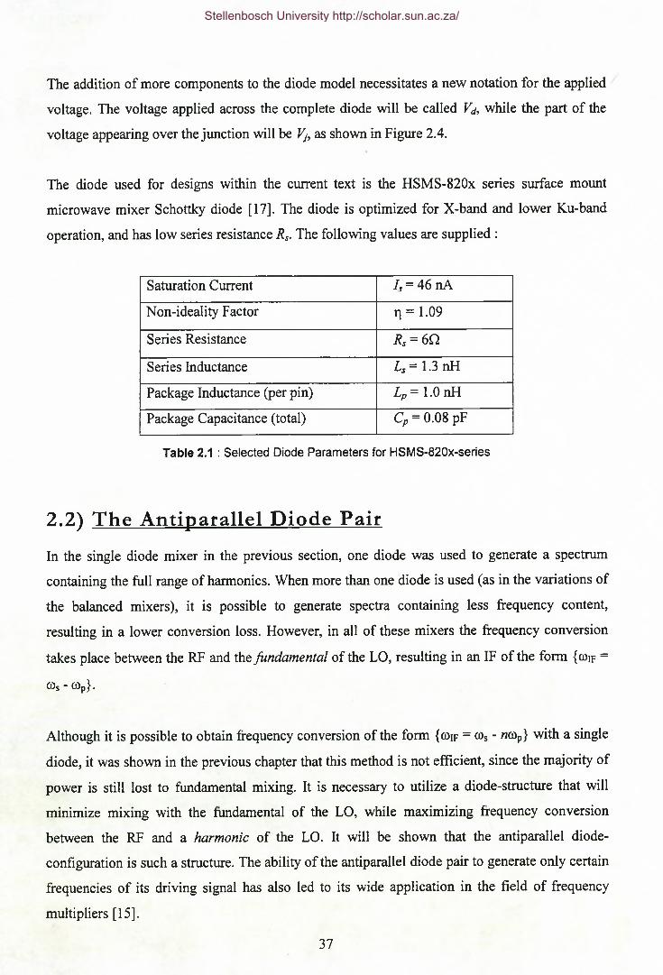
The addition of more components to the diode model necessitates a new notation for the applied
voltage. The voltage applied across the complete diode will be called Vd, while the part of the
voltage appearing over the junction will be Vj, as shown in Figure 2.4.
The diode used for designs within the current text is the HSMS-820x series surface mount
microwave mixer Schottky diode [17]. The diode is optimized for X-band and lower Ku-band
operation, and has low series resistance Rs. The following values are supplied :
Saturation Current 7s = 46 nA
Non-ideality Factor r| = 1.09
Series Resistance Rs = 6Q
Series Inductance Ls = 1.3 nH
Package Inductance (per pin) Lp = 1.0 nH
Package Capacitance (total) Cp = 0.08 pF
Table 2.1 : Selected Diode Parameters for HSMS-820x-series
2.2) The Antiparallel D iode Pair
In the single diode mixer in the previous section, one diode was used to generate a spectrum
containing the full range of harmonics. When more than one diode is used (as in the variations of
the balanced mixers), it is possible to generate spectra containing less frequency content,
resulting in a lower conversion loss. However, in all of these mixers the frequency conversion
takes place between the RF and the fundamental of the LO, resulting in an IF of the form {cdif =
cos - cop}.
Although it is possible to obtain frequency conversion of the form {©if = cos - mop} with a single
diode, it was shown in the previous chapter that this method is not efficient, since the majority of
power is still lost to fundamental mixing. It is necessary to utilize a diode-structure that will
minimize mixing with the fundamental of the LO, while maximizing frequency conversion
between the RF and a harmonic of the LO. It will be shown that the antiparallel diode-
configuration is such a structure. The ability of the antiparallel diode pair to generate only certain
frequencies of its driving signal has also led to its wide application in the field of frequency
multipliers [15].
37
Stellenbosch University http://scholar.sun.ac.za/

2.2.1 Single Diode Fundamentals
To understand the fundamental operation of the antiparallel diode pair, it is necessary to briefly
consider the operation of a single diode. Figure 2.5 shows the junction conductance g(t) for a
single diode driven by an LO signal.
The junction conductance reaches a maximum once during every LO cycle, and by taking the
Fourier transform of the conductance waveform g(t), it is evident that the diode’s junction
conductance changes periodically at the frequency of the LO. It is this mechanism that controls
the mixing action of the single diode and balanced mixers.
Figure 2.5 : Conductance waveform g(t) for a single diode
2.2.2 The Antiparallel Configuration
When two diodes are joined in parallel as shown in Figure 2.6, an antiparallel diode structure is
created [2], It will be shown that gp, the conductance of the diode pair, provides the mechanism
for “higher order mixing”, i.e. frequency conversion with harmonics of the LO [2],
38
Stellenbosch University http://scholar.sun.ac.za/

Using the notation of Figure 2.6, and using intrinsic diode models for the purpose of the
discussion, the differential conductance of the diode pair is given by taking the derivative of the
instantaneous current ip with respect to the voltage Vp, or
(2.10)
The individual diode currents idi and combine as follows to form the ip, the diode current for
the pair of diodes (Figure 2.6):
(2.11)
The loop current ic flows inside the loop, and will be considered in the following sections.
Expressions for the diode pair conductance, gp, will now be developed. Once the input
impedance of the diode pair can be expressed in terms of ip and the techniques of mixer
analysis and design can be implemented in the usual fashion.
Equation (2.11) can be expanded as follows using equation 2.6 (note that the series resistance Rs
has been omitted for the purpose of this investigation; its effect will be considered in later
It is assumed that the two diodes of the antiparallel pair are identical. Although the diode pair is
usually fabricated on the same wafer (and therefore the diodes have very similar Is, r| and Rs),
sections):
(2.12)
this assumption is only valid to a certain extent. The effect of diode unbalance will be considered
separately. Equation (2.12) can be reduced to [2]
(2.13)
39
Stellenbosch University http://scholar.sun.ac.za/

where a is known as the diode slope parameter, and represents the effect of the non-ideality
factor T) and temperature T. For the HSMS-series diodes used for designs within the current text,
the diode slope parameter is a = 3 4 F '7.
Since the voltage Vp is known, and the current ip can be expressed in terms of Vp, it is possible to
find the conductance gp of the antiparallel pair using equation (2.10) :
8 = g, + = —— + ^-dl ............. (214)p dV dV
P P
Note that the parallel conductances simply sum to the total conductance. Using equation (2.13) it
is possible to reduce equation (2.14) to
gP - [ f Vp + e~aV") = cosh (a Vp ) ............. (2-15)
Inspection of equation (2.15) reveals that the conductance gp has even symmetry around Vp (due
to the co.s/?-function), and as a result reaches two positive peaks for every one positive peak of
the LO. Figure 2.7 shows the junction conductance g(t) for the antiparallel diode pair.
Figure 2.7 : Junction Conductance g for Antiparallel Diode Pair
40
Stellenbosch University http://scholar.sun.ac.za/

2.2.3 Two-Tone Analysis
During normal mixer operation, the driving voltage Vp(t) of the antiparallel pair consists of the
sum of the large signal LO and the small signal RF. Mathematically this signal can be expressed
as
Vp(t) = VLO cos(coLOt) + Vs cos(a)st) ............. (2.16)
The junction conductance g(t) is modulated by only the LO voltage, and therefore equation
(2.16) can be reduced to
Vr(t)- .V l0 cos(au; ) .............(2-17)
Substituting equation (2.17) into equation (2.15) produces
gp = 2a Is cosh (aVLO cos(a>LOt)) .............(2.18)
which can be expanded into [2]
k(ccVL0)
g p = 2 a l s +212 ( aVL0 ) cos(2coLOt)
+2IA(aVLO)cos(4co LOt ) + -
(2.19)
where I„(cxVlo) are modified Bessel Functions of the second kind [5]. At this stage the junction
conductance waveform g(t) of the antiparallel diode pair can be described completely in terms of
the modulating voltage Vp. It is noteworthy that g(t) consists of a dc value described by the first
term in equation (2.19), as well as harmonics at the even frequencies of the LO. To find the total
current (large- and small-signal) flowing in the antiparallel diode pair, it is necessary to
“superimpose” the complete driving voltage Vp onto the conductance waveform gp(t). Using
Ohm’s law, and from equation (2.16)
ip = g p (0 x (VL0 cos(coLOt) + Vs cos(cost)) ............. (2.20)
and by substituting equation (2.19) into equation (2.20), the total current for the diode pair is
41
Stellenbosch University http://scholar.sun.ac.za/

1P = Acos{c0w t)+ Bcos(cost)+Ccos(3coLOt)+ Dcos{5coLOt) + E cos(2coLO + o)s )r + F cos(2coLO -cos )t + G cos(4<yi0 + cos )t + H cos(4«i0 -cos )t + ... (2 .21)
where A, B, C, ...are at this stage arbitrary coefficients. From equation (2.21) a number of
noteworthy observations are made. From inspection it becomes clear that the composite current
ip flowing through the antiparallel diode pair contains only components with frequency
{mcos6ncDLo} where (m+n) = 1,3,5, ...i.e. an odd integer. Equation (2.21) mathematically displays
the mechanism by which the antiparallel diode pair converts an RF signal to an IF signal using a
multiple of the LO, e.g. coIF = cos ~ 2colo or co]F = 4a>L0 - cos• Since the amplitude of the RF
signal is usually both fixed and small, harmonics of the RF signal other than the first are
impractical to use.
Figure 2.6 also indicates that a loop current ic circulates within the loop formed by the
antiparallel diode pair. Because of the assumption of identical diodes ic can be expressed as
i = ld\ ld l . (2 .22)
Using the usual trigonometric identities and equation (2.6), equation (2.22) can be expanded into
= l s (cosh(aVp)~ 1) (2.23)
which can in turn be expanded using equation (2.16):
c 2
V2 + V 2 V2 s V2 / xLO 2 S + ~ Y cos(20)LOt ) + cos(2cost)
LO S {C0S(' > + cos(<yLO +cos }
+ cos(3coLO - cos )t + cos(3coLO + a)s )r +...}
(2.24)
42
Stellenbosch University http://scholar.sun.ac.za/

Important observations are made from inspection of equation (2.24). The loop current ic flowing
within the loop formed by the antiparallel diode pair contains only components with frequency
{ma>s6ncoLo} where (m+n) = 0,2,4,..., i.e. an even integer. Equation (2.24) contains the
mechanism by which the antiparallel diode pair suppresses the even harmonic mixing products,
e.g. coif = cos - colo or coif = 3c o lo ~ &>s, as well as the even harmonics of the LO, e.g. Icolo >
4(oLo , etc.
2.2.4 IF Frequency Spectrum
Figure 2.8 shows the typical output spectrum of the antiparallel diode pair driven by LO and RF
signals. It is significant to note that the first harmonic of the LO is located relatively far from the
IF, i.e. there is no significant frequency content between the IF and the LO. It is therefore easy to
realize a low-pass filter to extract the IF from the mixer. This is a very desirable characteristic of
harmonic mixers.
When compared to the output spectrum of typical double balanced diode mixers (Figure 1.6), it
is clear that the frequency content in the output spectrum is significantly reduced due to the
suppression of certain frequencies. It is important to note that this suppression is reduced by
diode unbalance', a factor that may become significant when the mixer is realized. Diode
unbalance will be discussed in section 2.6.
This concludes the fundamental description and characterization of the antiparallel diode pair. It
is clear that the antiparallel diode pair is an ideal “building block” for a harmonic mixer : it
permits current containing only odd harmonics of the LO (and mixing products with m+n odd) to43
Stellenbosch University http://scholar.sun.ac.za/
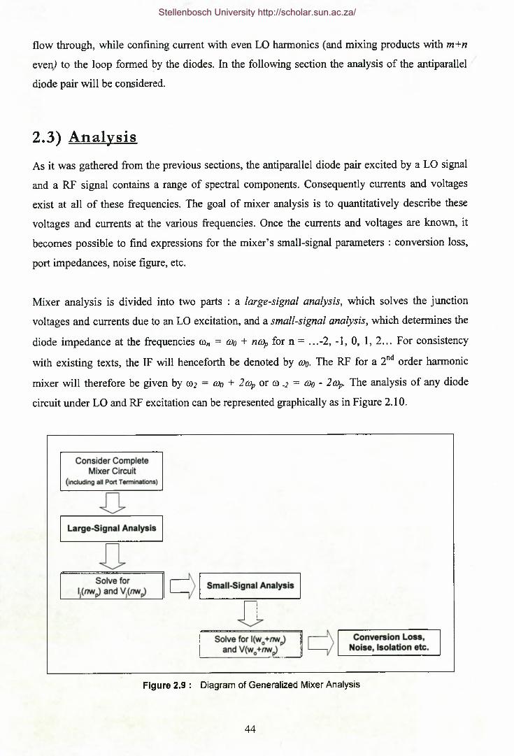
flow through, while confining current with even LO harmonics (and mixing products with m+n
even) to the loop formed by the diodes. In the following section the analysis of the antiparallel
diode pair will be considered.
2.3) Analysis
As it was gathered from the previous sections, the antiparallel diode pair excited by a LO signal
and a RF signal contains a range of spectral components. Consequently currents and voltages
exist at all of these frequencies. The goal of mixer analysis is to quantitatively describe these
voltages and currents at the various frequencies. Once the currents and voltages are known, it
becomes possible to find expressions for the mixer’s small-signal parameters : conversion loss,
port impedances, noise figure, etc.
Mixer analysis is divided into two parts : a large-signal analysis, which solves the junction
voltages and currents due to an LO excitation, and a small-signal analysis, which determines the
diode impedance at the frequencies to„ = a>o + no), for n = ...-2, -1, 0, 1, 2... For consistency
with existing texts, the IF will henceforth be denoted by coq. The RF for a 2nd order harmonic
mixer will therefore be given by to 2 — coo + 2cop or co .2 = (Do - 2cOp. The analysis of any diode
circuit under LO and RF excitation can be represented graphically as in Figure 2.10.
Figure 2.9 : Diagram of Generalized Mixer Analysis
44
Stellenbosch University http://scholar.sun.ac.za/

The following discussion of mixer analysis will follow the topology presented in Figure 2.10.
Once the large-signal and small-signal analysis have been done, the mixer performance will be
related to the “figure of merit” mixer properties introduced in Chapter 1.
2.3.1 Large-Signal Analysis
The first step in the analysis of the diode circuit is a large-signal analysis. The junction of the
diode(s) contains both a conductance and a capacitance that are strong nonlinear functions of the
diode junction voltage V/t). It is required to solve the currents through these elements at the
various frequencies of the applied junction voltage. Once the currents and voltages are solved,
the Fourier components of the junction conductance can be calculated, and simultaneously the
junction conductance waveform g(t) can be computed, i.e. a time-domain waveform of the
pumped diode conductance can be obtained. Although it is the Fourier components rather than
the time-domain waveform that are used in the following small-signal analysis, the shape of g(t)
can nevertheless provide useful information regarding the order of the change in conductance as
the junction is pumped by the LO.
Various techniques to obtain the voltages and currents at the LO have been presented. [18, 19,
13]. The harmonic balance technique has evolved to a very robust solution algorithm, and is the
most popular technique used in modem software packages. This technique will be presented in
the following section. Although not as popular as the HB (harmonic balance) technique, the
reflection algorithm [20] remains a useful tool in large-signal analysis, and is included in
Appendix A for completeness.
2.3.2 Harmonic Balance for Single Diode [18.191
The harmonic balance technique determines the junction current and voltage at each LO
harmonic by “balancing” the currents of the linear and the nonlinear parts of the diode circuit. A
brief overview of the HB technique for a single diode will be given, whereupon the technique
will be modified for the antiparallel diode pair.
The aim of the technique is to find the time-domain junction voltage V/t), or alternatively
Vj(ncop) for n = ..., -2, -1, 0, 1, 2, ... in the frequency domain, where cop represents the LO. Once
the junction voltage is known, the junction current Id(t) or Id(ncop) is also known.
45
Stellenbosch University http://scholar.sun.ac.za/

The large-signal junction characteristics are completely described in terms of the large-signal
junction voltage V, by the following equations :
W = /oqv, \
> * T - \ . (2.25)
W = c , odV;dt
, (2.26)
where
dQiC(V ) = ——
V dV.cj 0
V i\ / /2
\ <Pb<i
(2.27)
The circuit that will be analyzed usually contains a diode junction embedded within a linear
network. This linear network includes the diode series resistance, package parasitic impedances,
the matching networks, and any source and load impedances (usually the RF source and IF
terminating impedance). Figure 2.11 shows the typical setup with LO source, IF and RF
terminations (large signal excitation, therefore no RF signal is applied), and the complete diode.
Diodewith
Package
Figure 2.10 : Equivalent Circuit of Mixer with Single Diode
By manipulating the elements shown in Figure 2.11, it is possible to divide the entire circuit into
a linear part and a nonlinear part. The linear part will include the LO source, all terminating
impedances (Zs, Zrf and Zif), the entire matching circuit, the linear time-invariant components of46
Stellenbosch University http://scholar.sun.ac.za/

the diode package, and the diode series resistance Rs. The nonlinear part will consist of the
junction conductance (modeled as a voltage dependent current source Ig(Vj)) in parallel with the
nonlinear capacitor Cj(Vj). The entire linear circuit (with the exception of the LO source) can be
expressed as a row matrix Ysfnatp) with its elements equal to the equivalent complex admittance
at the harmonics of the LO. Figure 2.12 shows how the circuit from Figure 2.11 can be
manipulated into a linear and a nonlinear part.
Once the circuit has been divided into a linear and nonlinear part, it becomes easy to understand
the fundamentals of the harmonic balance method. While the linear part of the circuit contains
time-invariant frequency dependent elements that is best described in the frequency domain, the
nonlinear part of the circuit contains a time-variant capacitance and conductance that is best
described in the time domain. An estimate of Vj is initially made at all the harmonics of the LO,
whereupon the linear and nonlinear harmonic currents, 7/ and /„/, are calculated. An error
function is created by the difference between 7/ and 7„/, and Vj is chosen repeatedly (usually by
means of a numerical method) until the error function is sufficiently small. Finally V/ncop) is
known for all the harmonics, and the large signal time-domain LO waveform V/t) can be
constructed.
From Figure 2.12 it is clear that the following condition (Kirchoff) must hold between the linear
circuit and the nonlinear junction :
7,(11©,)— 7* (»® ,) ............. (2.28)
for n = 0,1,2,... N, or in vector form :
47
Stellenbosch University http://scholar.sun.ac.za/

~I,( 0) ' I J O )
h(<»P) Ki(o3p)
I t( 2o>P) = - I J 2g>p)
I/fNcOp) J J N ( O p)
. (2.29)
The initial estimate of Vj will produce values of 7/ and /„/ that can be used to create the current-
error vector of the form
F(Vj) = // + Inl .............(2.30)
A numerical method is used to find V/ncop) so that equation (2.30) eventually becomes
F(Vj) = 0 ............. (2.31)
The computation of the current-error vector involves operations in both the time domain and the
frequency domain. The matrix of the time-invariant currents in the linear circuit is computed as
follows (from Figure 2.12):
(2.32)
The currents in the nonlinear junction arise from equations in the time domain. The nonlinear
current /„/ is made up of the resistive current Ig and the reactive current Ic, or
I n l - I g + I c
where Ig is defined by equation (2.6), and Ic is found using equation (2.3):
• _ d _ d lc 1 Qd j
dt dt
(2.33)
, (2.34)
Instead of finding the time-derivative using numerical techniques (which may be cumbersome),
the capacitor current is easily found in the frequency domain :
48
Stellenbosch University http://scholar.sun.ac.za/

(2.35)
where O is a diagonal matrix with (ncop) for n = 1,2,3, ... JV on its diagonal axis. The current-error
vector F(Vj) can now be computed in the time domain :
F(Vj) = 3 {I i} + i„i .............(2.36)
The numerical technique for finding Vj to satisfy equation (2.36) can be one of a variety of
optimization techniques [9]. The Newton-Raphson iteration is used most commonly. After p
iterations Vj is described by Newton’s method as follows (in the time domain):
VjP+I = Vjp -J '^ F fV j) .............(2.37)
where J is the Jacobian matrix, defined as
J = — F(V.) = Ye + .............(2.38)dVj ' E dVj J dVj
Vj is found using various matrix manipulations of its comprising terms. Since only an overview
of the method is presented here, these manipulations are omitted.
Once the voltage Vj is solved for all the harmonics of the LO the junction can be completely
characterized in terms of its voltage Vj(ncop) and current Ij(ncop). Since Vj is known, it is possible
to find the junction conductance waveform gj(t) via equation (2.25), as well as the junction
capacitance waveform Cj(t) via equation (2.27). As mentioned at the beginning of the section, the
Fourier components of the total junction conductance G(jcop) at the harmonics of the LO can now
be found from Ohm’s law :
and the time-domain junction waveform g(t) can be found through taking the inverse Fourier-
transform of equation (2.39).
49
Stellenbosch University http://scholar.sun.ac.za/

Using the HB method to solve the junction currents and voltages of the antiparallel diode pair
involves only slight alterations of the technique for a single diode described above, as will be
shown in the next section.
2.3.3 Harmonic Balance for Antiparallel Diode Pair
When analyzing the antiparallel diode pair, one essentially has to analyze a circuit containing
two diodes, and therefore two nonlinearities. Although the basic analysis remains the same (such
as described in the previous section), there are two possible methods, depending on the
complexity of the problem :
- The circuit can be reduced to a single nonlinearity, and analyzed in a way similar to a
single diode;
- The circuit can be treated as a multiport network, and analyzed accordingly.
While the first method often only caters for trivial solutions, the second method accommodates
for a non-trivial circuit. The second method will be presented first.
2.3.3.1 Multiport Network [13]The expansion of a mixer with an antiparallel diode pair into a multiport network is similar to the
representation in Figure 2.12. The entire embedding circuit is connected to the two diodes A and
B via a series of ports. These are not physical ports, but rather ports representing the various
harmonics of the LO. Figure 2.13 contains such a representation.
50
Stellenbosch University http://scholar.sun.ac.za/

Diode A is connected to the linear network through a series of ports at the frequencies neap (for n
= 0, 1, representing the harmonics of the LO. Diode B is connected in a similar
fashion. The LO is applied at port C, similar to the single diode mixer.
The analysis of the multiport is similar to the previous analysis, except that vectors are now
replaced by vectors of vectors. The linear current vector of equation (2.29) now become vectors
of current vectors, or
where, for instance, I ij is the matrix
51
Stellenbosch University http://scholar.sun.ac.za/

I , A =
1,(0)I,(cop)I,(2(op)
I,(Ncop)
.(2.41)
Similarly the nonlinear current vector of equation (2.29) becomes
h i =nl,A
nl,B
. (2.42)
Note that no nonlinear current component flows in port C. The estimated voltage (Vj in the
previous section) is also put in vector format:
V = (2.43)
In a way similar to equation (2.32), the linear current components // are found as follows :
I ^ Y V ............. (2.44)
where Y is a 3-by-3 matrix with sub-matrixes similar to Ye- The nonlinear current components
are found by solving equation (2.42) (effectively solving for each diode separately). Once the
linear and nonlinear current components are known (for a specific value of V), the error function
F can be minimized, eventually solving for VA and VB.
It is clear that the obtaining the large-signal solution for the antiparallel diode pair via the
multiport method is merely a “matrix-extension” of the harmonic balance method for the single
diode. The alternative to the multiport method, i.e. the equivalent diode method, will now be
considered briefly.
52
Stellenbosch University http://scholar.sun.ac.za/

2.3.3.2 Equivalent DiodeThe equivalent diode method evaluates the entire mixer circuit at every harmonic of the LO, and
produces an equivalent (and usually rather simple) circuit containing only one diode. The
analysis for a single diode described in section 2.3.2 can then be applied almost exactly. A
drawback of this analysis is that it is often limited to a specific mixer, and is therefore not
generic like the multiport method. The equivalent diode method can justifiably be viewed as a
specific case of the multiport analysis.
Since the equivalent diode method is often specific to a certain mixer configuration, its
implementation will be demonstrated using a specific mixer. Figure 2.14 shows a typical
topology for a harmonic mixer. The antiparallel diode pair (consisting of identical diodes A and
B, with their series resistance Rs and series inductance Ls) is driven by an LO source with
impedance Zlo■ In general, the impedance Zlo can represent the termination for a number of
source and load impedances.
The key to the successful implementation of the equivalent diode method for this circuit lies in
the symmetry of the configuration. The circuit as seen by the LO is symmetrical, except for the
polarity of the diodes. This causes the even order LO harmonics to be out of phase over the
diodes, producing zero voltage over the parallel LO branch. The odd LO harmonics are in phase
over the diodes, producing a voltage over the parallel LO branch [21]. The equivalent circuits
seen by each diode at the various LO harmonics are summarized by Figure 2.15.
53
Stellenbosch University http://scholar.sun.ac.za/

The matrix h(ncop) of equation (2.29) representing the linear current components can now be
constructed using the circuits of Figure 2.15. The remainder of the analysis, i.e. the nonlinear
current components, minimization of the error function, and solution for V(na>p), is conducted
exactly according to the process described in section 2.3.2.
On completion of the large-signal analysis, the set of harmonic voltages Vj = V/ncop) and
harmonic currents Id = Id(ncop) for n = 0,1,2,... are known. In the next section it will be shown
how the small-signal parameters for the antiparallel diode pair is obtained once the large signal
analysis has been done.
54
Stellenbosch University http://scholar.sun.ac.za/

2.4) Small-Signal D iode Parameters
Once the LO is solved in the way described in the preceding section, all large-signal quantities
are known, and the small-signal analysis is done. Defining the small-signal impedances of the
mixer involves not only the LO frequency cop (as was the case with the large-signal analysis), but
also the IF frequency coo• The small-signal analysis will give the input impedance to the mixer at
all the frequencies co„, where
g)„=coq + ncop ............. (2.45)
and n is the n-th LO harmonic. The list of input impedances can be calculated most effectively
through matrices, which gave rise to the term "conversion matrix Conversion matrices are first
generated separately for the junction conductance and junction capacitance of the separate diodes
(thus a total of four matrices, of which two pairs are identical in the ideal scenario of balanced
diodes). Thereafter the admittance matrix Ye for the embedding network (Figure 2.13) of the
entire mixer is constructed (the admittance matrix is used instead of the impedance matrix,
allowing admittance components to be simply added together). Finally the conversion matrix YM
for the entire mixer (including the antiparallel diode pair) is constructed.
2.4.1 Conversion Matrix for Junction Conductance
The voltage across the junction can be represented by a set of time-domain phasors v(t) given by
[9]
V f t > = t r „ Z ( K + m > , ) / ) = t .................(2 -46)tt=-co AJ=-oo
where V„ is the voltage component at frequency co„ (obtained by the HB method)and a>o is the IF
frequency. Note that the waveform v(t) is a sum of phasor quantities - effectively a summation
of sinusoids of magnitudes and angles contained in V„, and with frequency given by (coo + ncop).
v(t) is expressed here as a complex function in the time-domain. In a similar way the current
through the nonlinear conductance is defined as
i(t) = Y ........... (2.47)YI- - C O
55
Stellenbosch University http://scholar.sun.ac.za/

From the definition, the Fourier series of a time-varying resistance r(t) is
r ( t ) = £ V ” " (2.48)n=-oo
The /?„-elements are the small-signal values for the junction resistance. They are found using
equation (2.7) (section 2.1.2.2). r(t) therefore represents the time-domain waveform of the
resistive part of the diode junction, as the diode is pumped by the LO.
Using Ohm’s law, the relationship between equations (2.46) - (2.48) is given by equation (2.49).
Note that the number of harmonics n has been limited to a finite number so that n = -N, N.
This corresponds to the number of harmonics used in the large-signal solution. In matrix
notation:
11•
11G0 ••• G_2n
Q n G0
-N
(2.49)
or
/ = GjV (2.50)
The elements of the junction conductance conversion matrix Gj are a function of both the LO
frequency cop and the applied IF signal, and provides the solution to the small signal impedance
of the junction conductance for the frequencies co„ = coo + ncop for the first N harmonics.
2.4.2 Conversion Matrix for Junction Capacitance
The small-signal voltage over and current through the junction capacitance are again given by
equations (2.46) and (2.47). The small-signal junction capacitance is given by equation (2.9):
dt dt dt
56
Stellenbosch University http://scholar.sun.ac.za/

Similar to equation (2.50), the small-signal voltages and currents for the junction capacitance are
related by the following equation :
/ = jQ CjV .............(2.51)
where Cj is the junction capacitance conversion matrix (similar to the conductance conversion
matrix of equation 2.49). Q is a diagonal matrix with elements jncop, accounting for the
frequency dependence of the impedance presented by the junction capacitance. The elements of
matrix Cj are the Fourier components of the time-varying capacitance. Therefore jOC] provides
the small-signal impedance of the junction capacitance for the frequencies con = coo + ncop over
the first N harmonics.
2.4.3 Mixer Conversion Matrix
Instead of treating the antiparallel diode pair separately from the rest of the mixer, it is preferred
to find a conversion matrix representing the entire mixer. This is done to assist subsequent small-
signal analysis [22].
The process of generating the small-signal conversion matrix for the entire mixer can be better
understood when the mixer is once again treated as a multiport network (section 2.3.3.1). Figure
2.13 is altered slightly to make provision for the additional frequencies. Figure 2.16 shows the
new model for the mixer.
Figure 2.16 shows the entire mixer circuit including the antiparallel diode pair (diodes A and B
with their series resistances Ra and Rb respectively). The diodes are evaluated at frequencies
co0+ncop. This evaluation consists of the large-signal and small-signal analysis described in the
above sections, and is represented by the various “ports” between the diode and the remainder of
the mixer circuit. This remainder, or embedding network Ye, contains the diodes’ series
resistances, all matching networks, etc., and is evaluated at frequencies a>0+ncop using linear
circuit analysis. It is significant that port C (representing the source and load impedances)
contains more ports than the single port it contained for the large-signal analysis. This facilitates
the small-signal analysis of the mixer at frequencies o)0+n£op.
57
Stellenbosch University http://scholar.sun.ac.za/

/
For a typical harmonic mixer the following holds for port C:
- coo represents the IF and Yo is the IF-port admittance with Yo = 1/50 Q;
{cOo+2cOp} is the RF frequency, with Y2 = 1/50 Q;
- The remainder of the ports represents the various mixing frequencies, and are either not
considered if they are significantly small, or are reactively terminated, short- or open-
circuited, depending on the design.
The first step to finding the complete mixer conversion matrix is to determine the conversion
matrices separately for the two diodes, A and B. The junction conversion matrices are found
from equations (2.50) and (2.51), and the conversion matrices for the entire diode (excluding
package parasitics) are then found by summing the corresponding elements of equations (2.50)
and (2.51), or
Ya = G ja + J co C j A
YB= G jB+j(oC jB, (2.52)
58
Stellenbosch University http://scholar.sun.ac.za/

In order to illustrate the method, a harmonic mixer circuit is analyzed using only two harmonics.
The conversion matrix for diode A, Ya, is constructed as follows :
(GJa+jco0CJo) [Gj + jcoQCu) (Gu +ja>0CjJ (Gu +ja>0Cu ) (Gu +ja>0Cu )
(Gj, + j(°\C^) (GJo + M C Ja) (Gu + M c u ) {Gu + M c u )
Ya = (Ga + jco2Ch ) (G , + j(o2Ch ) (GJa + jo)2CJa) (Gu + jco2Cu ) (Gu + jco2Cu )
(Gh +jco,Ch ) ((Gh +jco3Ch ) [Gh +jcoiCJi) (G,o + ja>3Ck ) (GM + j a 3Cu )
(GJt+ jo )4C j (Gh +ja>4Ch ) (<Gh +j(o4Ch ) (G;| +j(oACJ) (Gjo+ jco4CJo)
where for example G,^ is the junction conductance evaluated at co„=.2 = <x>o - 2 cop, and 0)3
represents the frequency d)n=3 = coo + 3cop. The conversion matrix for diode B is constructed in a
similar way, and when the diodes are identical, Ya = Yb.
The conversion matrix for the embedding matrix, Ye, is found relatively easily from linear circuit
analysis. However, since there are three ports to be considered (A, B and C), special care has to
be taken when defining Ye- The most popular notation constructs Ye as a 3-by-3 matrix
containing nine individual sub-matrices. Ye is defined as follows :
yAAE
yA Bl E
yA C 1 E
II yBA yB BI E
y B C 1 E
1
yC Bl E 1
, (2.53)
The sub-matrices represent the relation of the different ports to each other, and have the general
form YEpor‘)(port>((On)- YeAA, for example, represents the input admittance of the embedding
network at port A for the frequencies con = a>o + ncop, while YeAC represents the admittance of the
embedding network from port A to port C. The sub-matrices of Ye are diagonal matrices, since
the linear network implies no coupling between the various frequencies inside the embedding
network [22]. The sub-matrices are the same size as the diode conversion matrices, i.e. with
dimension 2N+1 when N harmonics are considered.
The final step in setting up the mixer conversion matrix is to add the conversion matrices of the
individual diodes to the conversion matrix of the linear network. By coupling the diodes in
parallel with the embedding network (the typical topology, denoted by Figure 2.16), the diode
59
Stellenbosch University http://scholar.sun.ac.za/

conversion matrices can be added to the conversion matrices representing the embedding
network’s input impedance presented to the diodes, i.e. YeAA and YeBB. Equation (2.53) therefore
becomes
1
+
iyAB J E
Oi
II \rBAJ E rEBB+ Y B
y B CJ E
i *1
yC BJ E
o1
where Ym is the compound conversion matrix of the entire mixer. Note that the addition of the
diodes to the embedding network does not alter the coupling between the various ports, and
therefore the remainder of the sub-matrices of Ye is unaffected by the addition.
The mixer conversion matrix can be inverted to find the mixer impedance matrix, or [22]
= [ / « ] - ............. (2.55)
That concludes the small-signal solution of the mixer. In the following section Zm will be used to
find typical mixer parameters such as conversion loss, input impedance and VSWR.
2.4.4 Input Impedance
In Chapter 1 it was established that the diode’s input impedance is a function of both the LO and
RF signals (hence the terms small-signal and large-signal impedance). It is therefore only natural
to expect that the diode conversion matrix (which is the result of both a small-signal and large-
signal analysis) provides a convenient way of calculating the input impedance.
It will be necessary to distinguish between two different input impedances :
The mixer input impedance : The mixer input impedance is the impedance seen when
looking into a port of the mixer (typically the IF port). This impedance includes the
effects of both the antiparallel diode pair, and the embedding network.
- The diode input impedance : The diode input impedance is the impedance of the
antiparallel diode pair alone, excluding-the embedding circuit.
60
Stellenbosch University http://scholar.sun.ac.za/

The input impedance looking into any port (C,k) where cok = coo + kcop is defined as [22]
Zm = Z jS * x c * > ^ Z « : (k,k) ............. (2.56)
However, equation (2.56) includes the port admittance 7*, as shown in Figure 2.16. To obtain the
mixer input impedance, it is therefore necessary to remove the effect of F*, or
Zin = mk7 (C ,k)(C ,k) ‘
M TT (2.57)
The input impedance of the antiparallel diode pair will prove to be a quantity of interest during
the design of the harmonic mixer. In an oversimplified way it can be seen that the LO signal
dictates the impedance seen by an input port at the small-signal frequencies (a>s and &>„). Mixer
design then requires the correct embedding structure to ensure maximum power transfer at the IF
and LO. This topic will be handled in detail later.
2.4.5 Conversion Loss
In Chapter 1 conversion loss was defined as the ratio of output signal level to input signal level,
or
where iV is the IF output power ad Prf is the available RF power. Although conversion loss is
defined by this expression, a general expression for the conversion loss of a harmonic mixer
containing an antiparallel diode pair within an embedding network needs to be found.
Such an expression is found using the small-signal mixer analysis described in the previous
section [9], since the mixer impedance matrix Zm is already in a convenient form to carry out the
analysis. The specific method determines the conversion loss Lcfrom a specific sideband a>k = coo
+ kcop to the IF a>o. Usually the sideband in question will be the RF signal, and k = 2 for the
typical harmonic mixer.
61
Stellenbosch University http://scholar.sun.ac.za/

A small current is applied to the RF port (k = 2), resulting in a response at the IF port [22], This
small current is represented by
s i(C*)
and the resulting response at the IF port is given by
5V <C,0) = z (C’0)(C-k)S I(C’k) .............(2.58)
where Z j C’0)(C’k> is the impedance between the RF port and the IF port. The power available from
the RF source is given by
\si<c*> I2P „ =!------, - L .............(2.59)
where 7* is the input admittance of the RF source (from Figure 2.16) [9]. The IF output power is
given by
PIF= \5V (C^ R e { Y Q} .............(2.60)
where Yo is the termination admittance at the IF. Eliminating the small current S /c' > and small
voltage 5V<c’0> from equations (2.58) - (2.60), the conversion loss from the RF to the IF is found
to be
Lr> L —1 (2.61)
where k refers to the RF (but could refer to any frequency in general). Further quantitative
analysis of equation (2.61) will not be carried out in the current text, but further insight into the
calculation of the conversion loss can be gained by considering a method proposed by [9]. The
mixer is again divided into a linear and nonlinear part, as shown by Figure 2.17 :
The arrows indicate power flow through the circuit. The amplitude of the RF excitation signal Vs
can be expressed as
62
Stellenbosch University http://scholar.sun.ac.za/

V,=j8PTRe{Z,(jo,)} (2.62)
where Pt is the available power (unknown) that can be delivered to the pumped diode pair,
represented by Zp. The current flowing in the loop is found using the diode conversion matrix Zp:
/-(z,+z,yv. (2.63)
where Ze is the conversion matrix of the linear part of the circuit. The output power into the
embedding circuit represented by Ze at frequency con is
P , ^ \ l ( c , f Re{z,(jo>,)}
The conversion loss is now found using equations (2.62) and (2.64)
.(2.64)
4 = — pr T(2.65)
Figure 2.16 : Alternative Small-signal representation of Diode Mixer (with Power Flow)
2.5) N o ise
The fundamentals for mixer noise analysis have been established remarkably early. Although a
reliable model was only obtained in the 1970’s, the properties of noise correlation in mixers have
63
Stellenbosch University http://scholar.sun.ac.za/

been understood before that time. Since the topic of noise is an extensive field in its own right
[11, 14], the current text will only present the fundamentals.
In Chapter 1, mixer noise was categorized as either inherent noise, or signal noise. In Schottky
diode mixers the dominant inherent noise sources are :
1) Thermal Noise - Generated in the series resistance,
2) Shot Noise - Generated in the junction.
The dominant signal noise source for the Schottky diode is noise sidebands on the LO. In a
frequency mixer the noise-processes are rather simple to understand. The challenge arises when
the correlation properties of the noise is investigated. As it will become evident, the time-varying
junction creates the phenomenon by which the noise properties at all the mixing frequencies is
linked to one another - from there the idea of correlation.
2.5.1 Thermal Noise
As mentioned briefly in the preceding section, thermal noise has its origin in the series resistance
Rs. Thermal noise arises from the random agitation of electrons, and it is present in every
medium capable of dissipating power. Apart from being temperature dependent, thermal noise is
also frequency dependent, although it is the bandwidth B and not the absolute frequency that is
of importance.
The noise added to the diode circuit by a resistance R can be modeled by an equivalent voltage
source having the mean-square voltage given by
v2 = 4 KTBR ........... (2.66)
where K is Boltzmann’s constant and T is the absolute temperature [9]. The mean-square arises
from the fact that the noise is a random process, but can be characterized in terms of its average.
Note that equation (2.66) is only valid for non-cryogenic temperatures and frequencies below the
sub-millimeter range. Equation (2.66) is a generalization of Planck’s black body radiation law
[8] at the mentioned temperatures and frequencies. Figure 2.18 shows the Schottky diode model
adapted to include the effect of thermal noise.
64
Stellenbosch University http://scholar.sun.ac.za/

2.5.2 Shot Noise
The electrons crossing the junction of the Schottky diode cause the current waveform to be
approximated as a series of pulses, leading to the term “shot” noise. The instantaneous current
varies with time due to the random nature of the flow of electrons, but the average current
remains constant, and is a function of the dc current flowing through the junction.
The shot noise in a Schottky diode can be adequately modeled by an equivalent current source
(rather that a voltage source, as was the case with thermal noise). The mean-square equivalent
current source for the shot noise due to a current Ij flowing trough the junction is given by
i2 = Iq B Ij ............. (2.67)
where q is the charge of an electron. It must be noted that Ij is the current flowing through the
resistive part of the junction [9]. Once again frequencies in the sub-millimeter range are implied.
Higher frequencies reach the order of the inverse of the electron transit time across the junction.
Figure 2.18 also shows the Schottky diode model adapted to include the effect of shot noise.
Figure 2.17 : Adaptation of the Schottky Diode model to include the effects of shot noise and thermalnoise
2.5.3 Noise Correlation
Thermal and shot noise are treated as white Gaussian noise, therefore having a continuous and
uniform spectrum within the frequency band B. To demonstrate how frequency components of
the unpumped diode are not correlated, [9] dc-biased a Schottky diode, and created two noise
waveforms at different frequencies by applying band-pass filters to the diode’s noise. Since the
65
Stellenbosch University http://scholar.sun.ac.za/

original two noise waveforms are only a function of the dc bias, it follows that the resulting
mixing products are themselves functions of only the dc bias, and are therefore uncorrelated.
However, the situation changes once the diode is pumped by an LO signal. Although the thermal
noise remains constant under LO excitation (since the series resistance Rs remains constant), the
shot noise becomes a strong function of the applied LO signal. The shot noise “originates” at all
the harmonics of the LO, and is then converted to all the mixing frequencies by the process of
frequency mixing. Eventually the noise components at any mixing frequency include noise
components from all the other mixing frequencies, and the noise components are therefore
correlated.
The aim of an analysis will be to find the IF noise voltage due to the noise components from all
the mixing frequencies. This is done considering the thermal noise and the shot noise separately.
2.5.3.1 Shot NoiseFollowing the large-signal analysis and the solution of the junction current Ij(jcop), it is possible
to construct a matrix of noise currents at the mixing frequencies using equation (2.67). Using
analysis similar to the small-signal analysis carried out in the previous sections, the impedance
conversion matrix of the diode is related to the matrix of noise currents, resulting in the shot
noise voltage across the junction at any frequency com. Finally the shot noise correlation matrix
Cs is created, giving the correlation between shot noise at the various mixing frequencies [22,
23].
2.5.3.2 Thermal NoiseThe thermal noise does not vary with the applied LO, and is therefore uncorrelated at the various
frequencies. Following the same procedure as above, the thermal noise correlation matrix Ct
reduces to a simplified form of Cs. In effect C, becomes a diagonal matrix.
The total noise voltage for a single diode at any frequency is a sum of the thermal and shot noise
components, and employing C, and Cs the total noise power dissipated in the load Ze (Figure
2.17) at any frequency com is given by
66
Stellenbosch University http://scholar.sun.ac.za/

where v j is found using Ct and Cs. The single sideband noise temperature, or Tssb , relates the
total noise power to a single input source, and is a convenient way of expressing noise
performance for one input frequency :
Irn KBG„T s s B = T ^ r - .............(2-69)
where Gmn is the transducer gain between the input frequency con and the output frequency com
[9]. For the antiparallel diode pair, [22] defines the single sideband noise temperature as
where Z j C'0) is the input impedance to the mixer at the IF port and frequency, Y2 is the source
admittance of the RF signal, Z j '0)(C,2) relates the coupling impedance between the IF and RF
frequencies, C is the sum of the correlation matrices C, and Cs, B is the bandwidth, and the *T-
superscript indicates the conjugate transpose of the vector.
2.5.4 Signal Noise [241
The presence of noise sidebands on the LO is often a very real problem in receivers. The
sideband noise-components mix with the LO, producing low frequency mixing components
which are often situated very uncomfortably in the IF band (Chapter 1, Figures 1.8 and 1.9).
However, in Section 2.2.5 (Figure 2.9) the antiparallel diode pair’s ability to reject these mixing
products from the IF band was described. The noise sideband mixes with 2LO, producing mixing
products well outside of the IF band. This property is a function of the similarity of the diodes.
Simulation of the X-band mixer with identical diodes described in Chapter 4 shows typical
rejection values in excess of 105dB. Although a realistic figure will be less, the ideal figure will
be used for comparison in the following section.
Stellenbosch University http://scholar.sun.ac.za/

2.6) D iod e Unbalance
As with any balanced mixer, harmonic mixers suffer from the effects of diode unbalance. This
effect is caused by a slight variation in the characteristics of the diodes, mainly due to
manufacturing. This variation leads to unsymmetrical diodes, and the currents (and frequencies)
that were confined to the diode loop in the ideal case, begin to “leak” into the embedding mixer
circuit. The effects of diode unbalance have been investigated by [2, 25]. The most significant
result of diode unbalance is definitely a decrease in isolation.
Most of the diode parameters are subject to a certain degree of variation. [2] has investigated the
effect of variation in Is and tj, while [25] investigated a variation in Rs- The HSMS-8202 used for
the designs in Chapter 4 specifies variations for Cjo and Rs [17]. In the current text the variation
of these parameters will be investigated for the diodes used in the X-band 2nd-harmonic mixer
designed in Chapter 4. The parameter variations will be considered individually with reference to
the mixer’s performance.
2.6.1 Theory
The variation of the diode saturation current Is will now be expressed mathematically. Similar
derivations can be made for the other parameters, but they will be omitted here due to space
limitation.
[2] evaluates the effect of a variation in Is by comparing the resulting different conductances g. If
the difference in Is is denoted by AIS, the effective saturation currents for the two diodes become
Is i - Is + Als and Is2 = Is - AIs
respectively. From equation (2.15) the conductance for the pumped diode pair can now be given
by [2]
gP = 2 ccls cosh [otVp) + — - sink [ccVp) (2.71)
68
Stellenbosch University http://scholar.sun.ac.za/

The A/s-term introduces a sw/z-dependence to the conductance. The asymmetrical s/w/i-function
(as opposed to the symmetrical cos/2-function) provides the mathematical mechanism for the
unbalance effects.
2.6.2 Analysis
The effects of diode unbalance will now be investigated. The nominal values for the ideal
HSMS-8202 diodes will be used, and are given below. The typical deviations from ideality,
according to [17], are also indicated :
- Cjo = 0.18 ±0.04 pF
Rs = 6 ± 2 Q
- 77 = 1.09 ±0.02
- Is = 4.6e8 ±0.5e 8A
The mixer containing the HSMS-8202 is pumped at an optimal LO level. The simulated
conversion loss and isolation of selected frequency products are shown in the table below. The
{ © r f - cdlo} mixing product is an even order mixing product that should ideally be well isolated
from the IF.
Diode Parameter
Deviation
Conversion Loss
[dB]
LO-to-IF
Isolation [dB]{(Br f - CDlo}
Isolation [dB]
LO Noise
Isolation [dB]
Identical Diodes 7.2 30 140 11 0
ACjo = 0.04 pF 7.7 30 70 49
ARs = 2Q 7.5 30 88 45
At] = 0.02 7.3 30 100 74
AIS = 0.5e'8 A 7.2 30 110 90
Table 2.2 : Comparison of Mixer Performance for Diode Unbalance caused by variation of Diode Parameters. Only one parameter is varied at a time.
The results show that the mixer exhibits various levels of sensitivity to the diodes with unequal
parameters. As it was expected, the level of isolation is significantly influenced by unbalance,
while the conversion loss shows only slight deterioration. The unequal junction capacitance C7o
has the most profound effect on the level of unbalance, while the permitted variation in the
saturation current Is has an almost negligible effect on the isolation.
69
Stellenbosch University http://scholar.sun.ac.za/

2.7) The Antiparallel D iode Pair - A Quantitative
Analysis
Before the design of harmonic mixers is discussed in Chapter 4, a quantitative analysis of the
antiparallel diode pair is done. The aim of this analysis is to investigate the antiparallel diode pair
as a building block of harmonic mixers, and to become familiar with its performance. The
waveforms of the antiparallel diode pair under LO drive will be investigated, whereafter the
input impedance will be investigated. Finally a model for the antiparallel diode pair (which will
be used for the designs in Chapter 4) is extracted.
2.7.1 LO Excitation
Figures 2.19 and 2.20 show a typical large-signal solution for the voltage waveform Vj appearing
over the junctions of an antiparallel diode pair of HSMS-8202 Schottky diodes. For the purpose
of the investigation the diodes are assumed to have no parasitic inductance or capacitance, and
are driven at +3 dBm at a frequency of 5 GHz.
Figure 2.18 : Antiparallel diode pair LO time- Figure 2.19 : Spectrum of Antiparallel Diode Pair Waveform LO Waveform
From the above figures it is noted that the LO is made up of mainly the 1st and 3rd harmonics at
5GHz and 15 GHz respectively. Unlike that of a single diode, the LO waveform for the
antiparallel diode pair contains no dc component, and is symmetrical around the zero voltage
axis.
70
Stellenbosch University http://scholar.sun.ac.za/

The conductance gp(t) and capacitance Cp(t) waveforms occurring as a result of the applied LO
signal are shown in the figures below.
Figure 2.20 : Antiparallel Diode Pair Capacitance Figure 2.21 : Antiparallel Diode Pair Conductance modulated by LO modulated by LO
From Figures 2.21 and 2.22 it is clear that the conductance gp(t) plays the dominant role in the
mixer’s small-signal properties. The exponential characteristic causes the junction resistance to
vary from several ohms to tens of kilo-ohms, while the inverse square-root characteristic of the
junction capacitance only varies in the order of tens of picofarads. The conductance waveform
has a fundamental frequency of twice the LO frequency - it is this mechanism that forms the
heart of the antiparallel diode pair.
2.7.2 Large-Signal Input Impedance
By driving the antiparallel diode pair at various levels of power, a range of input impedances can
be achieved. By keeping the LO power fixed and varying the frequency, a clockwise rotation is
achieved on the smith chart (the effect of the junction capacitance). Figure 2.23 shows the traces
obtained for the pair of HSMS-8202 Schottky diodes in an antiparallel configuration driven at
power levels ranging from -lOdBm to +10dBm over a frequency range of 40 GHz. Figure 2.24
shows the comparative traces for a single Schottky diode (HSMS-8101) under the same
conditions.
From Figure 2.23 it can be seen that the antiparallel pair input impedance is governed by the real
conductance gp(t) for lower frequencies, but becomes a stronger function of the junction
capacitance Cp(t) as the frequency increases. At frequencies beyond 40 GHz the input impedance
becomes a function of almost exclusively the junction capacitance. Another phenomenon that is
confirmed by the comparison of Figures 2.23 and 2.24, is the greater input impedance for a given71
Stellenbosch University http://scholar.sun.ac.za/

LO power of the antiparallel diode pair when compared to the single diode pair. Due to its
parallel topology, the antiparallel diode pair has a greater junction conductance gP(t), while the
junction capacitance Cp(t) almost doubles. This is confirmed by Figure 2.25 below. The figure
shows a plot of the calculated capacitance for both a single diode, and an antiparallel diode pair.
Figure 2.22 : Input Impedance of Antiparallel Figure 2.23 : Input Impedance of Single DiodeDiode Pair as function of LO Power. The arrow as function of LO Power. The arrow indicates
indicates increased LO Power. increased LO Power.
Figure 2.24 : Junction Capacitance as a function of Junction Voltage Vj
for single diode and the Antiparallel diode
Smithd«p Mac
40GHz
9 *pM n0.01GHz
72
Stellenbosch University http://scholar.sun.ac.za/

When the frequency is kept constant (5 GHz) and the LO is swept from -10 dBm to +10 dBm,
the plot of Figure 2.26 is obtained for the antiparallel diode pair. It clearly shows how the input
impedance is a function of LO power.
Figure 2.25 : Input Impedance of the Antiparallel Diode Pair for swept LO Power at 5 GHz
When the input impedance curve of Figure 2.26 is divided into real and imaginary parts, the
plots of Figures 2.27 and 2.28 are obtained :
LO Power [mWjFigure 2.26 : Real part of the Antiparallel Diode Figure 2.27 : Imaginary part of the Antiparallel
Pair Junction Impedance Diode Pair Junction Impedance
From Figure 2.27 it is clear that there is an optimum real impedance presented by the antiparallel
diode pair. Matching of this point to the source impedance will ensure minimum conversion loss.
73
Stellenbosch University http://scholar.sun.ac.za/

2.7.3 Model
In order to carry out a successful mixer design, it is necessary to have an adequate model for the
antiparallel diode pair. Although the topology for the HSMS-8202 has been established earlier in
the chapter (Figure 2.4), it is necessary to verify the model with a measurement, and to modify
the model if necessary.
The parameter values for the model of the HSMS-8202 Schottky diode as given in Table 2.1
were verified by measuring the diode pair over 12 GHz, for LO power levels o f -10 dBm, OdBm
and +10 dBm. The diode was mounted in a jig comprising a SMA-connector on either side, and
the sets of measurements were taken. A sufficient model [26] was used for the SMA-connector,
and the measured diode model could be extracted from the measurements. The diode parameters
were optimized within their range of possible values [17], and finally a model for the HSMS-
8202 diodes was extracted. The traces for the different power levels are shown in Figure 2.29.
Figure 2.28 : Simulated Reflection Coefficient for the HSMS-8202 diode pair driven by LO levels o f-10 dBm (blue), 0 dBm (red) and +10 dBm (green)
The final model for the diode pair is shown in Figure 2.30. The unpumped diodes have a
resonance in the vicinity of 6 GHz, but this disappears as the diode is driven harder by the LO.
This model is used for the mixer designs in Chapter 4. Although more extensive topologies have
been suggested for the SOT-23 package [27], the model implemented in the current text proved
to be adequate.
74
Stellenbosch University http://scholar.sun.ac.za/

The optimization did not alter the values of the intrinsic diode parameters significantly, although
values for the package parasitics were altered slightly. The model is considered valid for
frequencies up to X-band.
Figure 2.29 : Final Model for HSMS-8202 Antiparallel Diode Pair
The operation of the harmonic mixer is now sufficiently characterized, and the antiparallel diode
pair is available as a well-defined building block of the mixer. The next chapter will move away
from the analysis of the harmonic mixer, and will investigate its synthesis. Chapter 4 will focus
on a practical implementation.
75
Stellenbosch University http://scholar.sun.ac.za/

Chapter 3 : Design Considerations
The fundamental requirement of a frequency mixer is frequency conversion. However obvious
this statement may seem, it is still the main task of a mixer to produce an output signal of lower
(or higher) frequency using the available two input signals. The quality of this produced output
signal will vary in accordance with the intended application.
Usually the primary requirement for the IF signal (in the case of a downconverter; an identical
argument can be presented for the RF signal in an upconverter) is adequate power of the output
signal - in other words, minimized conversion loss. The power of the applied RF signals is in
most instances minimal, since only a low-noise preamplifier is inserted between the receiver
antenna and the downconverter in a typical front-end application. Any RF power that can be
preserved by minimizing conversion loss does not have to be gained by excessive gain stages
(which are prone to noise and other forms of signal degradation).
Apart from minimal conversion loss, it is also preferable for a mixer to produce a clean IF
spectrum. Isolation from the LO and RF signals is usually the secondary requirement in mixer
design. Isolation is strongly associated with the topology of the mixer, as certain topologies
inherently produce IF signals which are “clean” of frequencies other than the IF (the balanced
mixer structures, for example, described in Chapter 1). However, the LO frequency usually
requires additional effort to be removed from the IF spectrum, due to its superior power
(typically the LO signal is larger in magnitude in the order of 20dB and more).
The available LO power is also a consideration which might be of concern. However, the choice
of a harmonic mixer usually implies an inherent LO power consideration, i.e. lower frequency
and higher power. It is therefore not often a problem to produce adequate LO power once the
type of harmonic mixer has been chosen, since the LO frequency usually lies in a region where
adequate power can be generated without additional effort.
Other factors such as input impedance and noise are rarely primary considerations for the design
of a mixer, and they are often implied in the design specifications. Even physical factors such as
size can be a consideration.
76
Stellenbosch University http://scholar.sun.ac.za/

Although it may seem as if the harmonic mixer design demands numerous requirements to be
met simultaneously, this is rarely the case. The proposed design procedure is to a large extent
modular, and design steps can be added or left out in accordance with the requirements.
However, before the design procedure can be developed, it is necessary to consider the possible
requirements for mixer design in depth. This is the done in the following sections.
3.1) “The D es ig n R equirem ent”
A mixer is designed in accordance with a set of requirements. These will now be discussed, with
emphasis on the requirement of low conversion loss and high port isolation. Due to its extensive
nature, and for lack of available space, this work will not consider the noise requirement as a
primary design consideration.
3.1.1 Frequency Allocation
The very first issue in the design of a harmonic mixer is the choice of frequencies. The primary
choice of frequency (i.e. the frequency that will dictate the choice of the others) lies between the
RF and the IF. No flawless argument can be presented as to which frequency needs to be fixed
first. On the one hand, the RF should be the primary choice, since the choice of RF is usually
dictated by the nature of the application (e.g. satellite communications, where frequencies need
to be confined to fixed frequency bands). On the other hand, the IF signal might be chosen first
due to the availability of components within the IF band (e.g. the GSM-band).
Once the RF and IF frequencies have been fixed, the LO frequency can be attended to. The
choice of LO frequency is generally dictated by the LO power availability. Should ample LO
power be available up to frequencies of half the RF, a 2nd-harmonic mixer can be utilized.
Should LO power be available to frequencies of only a quarter of the RF frequency, a 4th-
harmonic mixer can be employed. LO power at even lower frequencies can utilize a harmonic
mixer of orders higher than the 4th.
Once the IF is located at the correct frequency, the issue of minimal conversion loss can be
addressed.
77
Stellenbosch University http://scholar.sun.ac.za/
3.1.2 Ontimum Conversion Loss
The harmonic mixer’s conversion loss between two frequencies was defined by equation (2.61)
in Chapter 2 as
Apart from the numerical utilization of equation (2.61), it is significant to note that the following
three factors contribute towards conversion loss :
1. RF source termination (denoted by the factor Y j c,k)) : RF power can be lost before
even entering the mixer due to a mismatch between the RF source and the RF port. In
the examples presented later in the current work, care has been taken to always ensure
50Q at the RF port.
2. IF load termination (denoted by the factor Y/JC’0)) : The converted IF power can be
prevented to optimally “exit” the mixer due to a mismatch between the IF port and
the IF load. It is necessary to ensure that the resistive parts of the IF port impedance
and IF load impedance are ideally equal.
3. Coupling between conversion frequencies (denoted by the factor YJC'0)(C'k)) : Without
launching into an elaborate discussion pertaining to the mechanics of frequency
conversion in the antiparallel diode pair, it will be considered sufficient to say that
amongst others, the junction series resistance Rs adds to conversion loss by means of
resistive losses. The series inductance Ls does not have resistive losses, but becomes a
high impedance at higher frequencies, adding to the conversion loss. By the same
token the parasitic package components Cp and Lp also increase conversion loss.
From the above discussion it is clear that obtaining a low conversion loss can only partially be
achieved by optimum design. The diode characteristics play an important role in determining
conversion loss, and the correct choice of diode is essential to satisfying the requirement of
minimal conversion loss.
3.1.3 Port Isolation
Rejecting the LO, RF and certain mixing products from the IF port is the most important goal of
port isolation. A secondary goal is often to reject the IF signal from the RF and LO ports, since
78
Stellenbosch University http://scholar.sun.ac.za/
any resistive termination other than the IF port causes an increase in conversion loss. Often the
RF signal is also rejected from the LO port, again for the minimization of conversion loss.
Although the isolation requirements of the previous paragraph seem to be difficult to realize
simultaneously, the process is often less complicated than it seems. The subharmonic mixer
provides inherent isolation from even order LO harmonics, as well as odd order mixing products.
The use of open-ended and shorted stubs is often employed as a further means to isolate ports
from unwanted frequencies. Finally, the use of filter structures in addition to the aforementioned
methods generally provides all the isolation that is needed. The use of these methods will be
demonstrated in the design examples.
3.2) Choice o f D iode
The choice of diode(s) is an important part of the design process. Factors such as low conversion
loss and noise temperature are influenced significantly by the properties of the diode.
Since it is impossible to escape the effects of junction resistance and capacitance of real diodes,
or the effect of the parasitic package elements, it becomes necessary to minimize these through
diode selection. For the beam lead diodes typically used at X-band, the junction capacitance is
often the limiting factor : a minimum capacitance of 0.1 pF restricts the use of theses diodes to
under 30 GHz [9]. A series resistance of 5Q is typical, while a series inductance of InH is often
observed. Different diode structures (e.g. dot-matrix or point-contact) are used at higher
frequencies to minimize C,& Rs and Z$.
A common method used to express the frequency capability of the diode is by means of the cut
off frequency f co, where
f = ----- 1....... ............... (3.1)Jco 2ttCj0Rs
fco often proves to be no more than a guideline, and should be treated accordingly, i.e. as a first-
order diode choice [28].
The choice of diode can be simplified if the designer has a knowledge of the sensitivity of the
diode to the specific parameter. The following figures compare the sensitivities of the79
Stellenbosch University http://scholar.sun.ac.za/

antiparallel diode pair to junction capacitance Qo, series resistance Rs, non-ideality factor tj and
series inductance Ls. The comparison should serve as an example, as results will vary depending
upon the mixer circuits. Figures 3 .1 to 3 .4 show the results from the simulation. The HSMS-8202
antiparallel diode pair is used in a standard 2n -harmonic mixer configuration. It is pumped by a
5 GHz LO, and the IF power is measured as the RF is swept through 10 GHz to 50 GHz. For
every sweep one of the diode parameters is increased by a realistic amount.
Figure 3.1 : IF Output Power for variation in Junction Capacitance : Cp = 0.18pF (blue line)
and Op = 0.36pF (red line)
Figure 3.2 : IF Output Power for variation in Series Resistance : Rs = 6Q (blue line) and Rs
= 12Q (red line)
Figure 3.3 : IF Output Power for variation in Figure 3.4 : IF Output Power for variation in Diode Non-Ideality : 77 = 1.09 (blue line) and 77 = Series Inductance : Ls = 1 3nH (blue line) and
1.18 (red line) Ls = 1.6nH (red line)
From these graphs it can be seen that the diode pair is very sensitive to an increase in junction
capacitance, and therefore the capacitance is usually a quantity that manufacturers aim to
minimize. The specific configuration is moderately sensitive to an increase (doubling) of series
resistance, while more ideal diodes tend to produce a better conversion loss at lower frequencies.
Figure 3.4 shows that an increase in series inductance can actually increase diode performance at
the lower frequencies (due to better reactive matching), while the series inductance causes an80
Stellenbosch University http://scholar.sun.ac.za/

increase in conversion loss at higher frequencies as the effect of the inductance becomes more
prominent.
Such an analysis should provide the designer with the background for making an optimum
choice when considering various diodes.
3.3) D e s ig n T op o log ies
The antiparallel diode pair can be used in more than one configuration. The mechanism of the
harmonic mixing remains essentially the same, although the different topologies have inherent
advantages and drawbacks.
3.3.1 Series Topologies \2\
The series topologies consist of the antiparallel diode pair with one port on the one side, and two
ports on the other side. Figures 3.5 and 3.6 illustrate the two options offered by the series
topology.
Figure 3.5 : Isolated Series Topology
Figure 3.6 : Non-lsolated Series Topology 81
Stellenbosch University http://scholar.sun.ac.za/

3.4.1 Specifications
The design starts off with a set of specifications. These can include frequencies, limits for
conversion loss, port isolation, etc. The specifications enable the designer to consider and
possibly make choices concerning the topology, the order of the LO harmonic used, the method
of realization, etc.
3.4.2 Choice of Frequencies
The frequencies not stipulated by the initial specifications are now chosen. At this stage it is
important to consider any possible spurious responses generated due to a poor choice of
frequencies. Once the LO, RF and IF have been fixed, the next step is to choose the topology.
3.4.3 Topology
A topology is chosen, if it has not already been done in 3.4.1. This choice is influenced by
factors such as port isolation, intended complexity of the circuit, method of realization (e.g.
stripline), frequency bands, etc.
An outline for the intended design must also be constructed at this stage. Filters and matching
circuits need to be considered, and preliminary choices are made for the order of the filters, etc.
3.4.4 Choice of Diodes
It has been established that it is crucial to consider the specifications of the diodes used in the
design. In many cases this choice may be limited by the availability of the diodes. A low junction
capacitance is crucial for high frequency designs, while low series resistance is preferred for
lower frequency designs.
3.4.5 Basic Design
The goal of the basic design is to find the small-signal input impedances at the small-signal
frequencies. This is done in order to design the port filters and the matching networks. For the
basic design, the chosen topology is used with only two ports : a large-signal port for the LO,
and a small-signal port for the RF. With the circuit driven by the LO, and with the RF applied on
the small-signal port, the small-signal input impedances at the RF and LO ports are measured.
The spectrum at the RF port is also considered. A value for the LO power is chosen in the
84
Stellenbosch University http://scholar.sun.ac.za/

IF
Figure 3.7 : Shunt Topology
Since the shunt topology adds and extracts all the signals through one side of the antiparallel
diode pair, this sometimes necessitates the use of complex filtering structures, or diplexers.
Shunt stubs (like that of the series topologies) are seldom used.
3.3.3 Additional topologies
The series and shunt topologies were used to realize the majority of harmonic mixers
encountered in literature. Occasionally the antiparallel diode pair is used in a conventional
double balanced mixer structure, where the conventional single diodes are then replaced by the
back-to-back diodes [32]. The antiparallel diode pair has also been used in a triple balanced
mixer topology, resulting in a unique three-dimensional structure [33]. Quadrature mixers
utilizing antiparallel diode pairs have also been recorded [24].
3.4) D e s ig n Overview
Before the design examples are presented in Chapter 4, it is necessary to briefly consider the
design procedure developed for use in the current text. The procedure developed is to a large
extent a step-by-step design, starting with the design specifications and ending with the
realization of the design. Only the outline of the procedure will be given, as a detailed discussion
of each step is given in Chapter 4.
83
Stellenbosch University http://scholar.sun.ac.za/

3.3.1.1 Isolated Series Topology [3, 29]The isolated series topology of Figure 3.5 provides a very popular method for realizing harmonic
mixers. It has the IF and RF ports on one side of the diode (the small-signal side), and the LO on
the other side (the large-signal side). The separation of large and small signals provides a
convenient way of isolating the IF signal, contributing to this topology’s popularity.
The mixer utilizes two optional shunt stubs on either side of the antiparallel diode pair. On the
small-signal side the open-ended stub is 90° long at the LO frequency, presenting a short to the
LO (so that LO current flows through the diode pair), and at the same time removing the LO
from the small-signal side. On the large-signal side the shorted stub is 180° long at the RF
frequency, presenting a short to the RF frequency, and also providing a ground return path for
the IF signal.
3.3.1.2 Non-lsolated Series Topology [30]The non-isolated series topology is less popular due to the fact that additional measures need to
be taken to remove the LO from the IF port. If the LO and IF frequencies are far apart, this
becomes less of a problem. The non-isolated series topology may also utilize stubs, but the open-
ended and shunt stubs are interchanged. The non-isolated series topology has been implemented
in waveguide structures, where options are often reduced.
3.3.2 Shunt Topology [311
The shunt topology of Figure 3.7 is another popular mixer structure. It has all three ports
connected to one side of the antiparallel diode pair, while the other side is grounded. Sometimes
the LO and IF are respectively added and extracted through the same port, reducing the number
of physical ports to two.
82
Stellenbosch University http://scholar.sun.ac.za/

vicinity of minimum conversion loss (the datasheets usually provide typical values for LO
power).
Once the small-signal input impedances are known, the matching networks and filters can be
designed. The output spectrum is considered in order to establish the order of the required
filter(s).
3.4.6 Extended Design
The extended design adds another small-signal port, the IF port, to the topology. Since there are
now two ports in parallel (the RF and IF, or the LO and IF), it becomes difficult to match the
ports individually. This can possibly be overcome by a simultaneous solution or optimization. In
the current text, an approximation was made. Since one of the harmonic mixer’s characteristics
is frequency components (IF, RF and LO) that are spaced far apart, it is possible (within
reasonable bounds of the specific design) to consider only one of the shunt ports, while the other
is approximated as an open circuit (due to the effect of its matching circuit or filter). From this
principle, is it possible to design the output filters and matching networks for the IF and RF
ports, ensuring that the assumption is indeed met. The process will be illustrated in Chapter 4.
3.4.7 Simulation
After the initial design has been completed (usually with lumped elements or transmission lines),
it is necessary to simulate the entire circuit. If the assumption of 3.4.6 was not met by the initial
design, a second design must be carried out. It is also possible to optimize the circuit, especially
if it is simulated using non-ideal (e.g. microstrip or stripline) components. The effects of ground
straps, enclosures or possible unintended coupling between structures also need to be verified.
Another important factor to consider is the sensitivity of structures to component tolerances - if a
structure is more tolerant of dimensions etc. than can be met by the design procedure, it might be
necessary to consider an alternative.
After the design procedure has been carried out, the circuit can be realized. Two design examples
are presented in Chapter 4, and it was found that the above design procedure yielded very good
results.
85
Stellenbosch University http://scholar.sun.ac.za/

Chapter 4 : Implementation and Measurements
Two designs were carried out to demonstrate the principles discussed in the previous chapters,
one at S-band and one at X-band. A detailed exposition of the design process, with specific
reference to the design procedure presented in Chapter 3, as well as the results, will be presented
here for both cases.
4.1) S-Band Mixer
The first harmonic mixer design is for a S-band down-converting mixer. A number of
specifications are fixed for the mixer, setting out a basic direction the design procedure should
take. The design procedures for the filters implemented in the S-band mixer are given in
Appendix B.
The design of the mixer is done with the aid of Microwave Office. The design package includes,
amongst others, a large-signal circuit solver implementing the harmonic balance method, as well
as EM models for microstrip components, allowing the mixer to be simulated as a microstrip
circuit.
4.1.1 Specifications
An RF frequency of corf = 2.45 GHz is chosen, as this frequency falls in an ISM-band, is often
used for telemetry applications, and is also commonly used for applications such as WLL
{wireless local loop). The design will be for as wide a bandwidth as possible, although a value
between 100 MHz and 200 MHz would be sufficient. The IF is restricted to a value below 500
MHz, since available VHF components can then be used in the post-mixer stages. It was decided
to implement a 2nd-harmonic mixer.
4.1.2 Choice of Frequencies
With the RF fixed on coRF = 2.45 GHz, the LO and IF need to be chosen. The mixer will be a
lower-sideband mixer in order to keep the LO frequency as low as possible. Finally the LO was
fixed at value of colo = 1-1 GHz, which resulted in an IF with frequency
86
Stellenbosch University http://scholar.sun.ac.za/

colF = co^ - 2coLO = 250 MHz (4.1)
The choice of LO and IF allows a bandwidth of 100 MHz to 200 MHz, while the IF lies safely
within a frequency range where standard VHF components can be utilized. The choice of
frequencies can be summarized as follows :
CDpf = 2.45 GHz coLO =1.1 GHz coIF = 250 MHz
4.1.3 Topology
The next step in the design process is to choose a topology for the subharmonic mixer. Since the
isolated series-topology is a popular topology in the field of subharmonic mixers, this topology is
chosen for the S-band mixer.
It is further decided to follow the classic approach where the large-signal LO is isolated from the
small-signal RF and IF. The antiparallel diode pair will be pumped by the LO signal on one side,
while the RF signal and IF signal will respectively be injected and extracted on the opposite side.
A shorted stub will be used on the LO side, while an open stub will be implemented on the side
of the RF and IF. Figure 4.1 shows the intended topology.
Filters will be used on all three of the ports. This is a preliminary decision, and the intended use
of filters will be evaluated again when the spectra for all the ports are known. The IF is low
enough to implement a lumped-element low-pass filter, while the RF is high enough to
87
Stellenbosch University http://scholar.sun.ac.za/

implement a coupled-line band-pass filter. A low-pass filter, most likely consisting of distributed
elements, is proposed for the LO.
Finally, a relatively inexpensive microstrip substrate intended for use in the lower GHz-region is
chosen. It has the following characteristics :
er = 3.86 h = 0.787 t = 0.05
4.1.4 Choice of Diodes
The HSMS-8202 series Schottky diodes will be used exclusively in this text. Table 2.1 and [17]
provide a detailed description of the diode characteristics. The HSMS-820x series is ideally
suited for use in the intended application. It has a low series resistance Rs of typically 6 ohms,
and the junction capacitance Cjo is typically 0.18 pF, making it suitable for applications well into
X-band. Other suitable diodes include [27].
Although the HSMS-820x series are available in a variety of packages, the HSMS-8202 is ideal
for use in a subharmonic mixer. It comprises two antiparallel diodes, housed in a SOT-23
package. The characteristics of the entire diode (including package) are well defined in its
datasheets, and in Chapter 2 an optimal model for the diode was extracted from measurements. It
is this model that will be used in the design of the mixer.
4.1.5 Basic Design
The basic design of the S-band subharmonic mixer is shown in Figure 4.2 (Microwave Office
schematic). It comprises a large-signal port PI, the antiparallel diode pair SI, a small-signal port
P2, and the stubs TL1 and 7X2 (implemented as ideal transmission lines).
Using the setup of Figure 4.2, the next step is to find the port impedances of the circuit. An
initial value of+ldB m was chosen for the LO power, since this is suggested in the datasheets. A
nonlinear analysis is performed, and the port impedances are as follows :
z» C ‘ = (73+-'U8)n
z» C 2=(93+-'u -65)n
z«C=(43+-'4-62)n88
Stellenbosch University http://scholar.sun.ac.za/

Figure 4.2 : MWO layout of the Basic Design
Figure 4.3 shows a plot of the input impedance of the small-signal port from 100 MHz to 3 GHz.
The effect of the open stub can be seen, shorting the input impedance to ground at 1.1 GHz and
providing the required isolation between the LO and the small-signal port.
Figure 4.3 : Impedance on the Small-Signal port
Figure 4.4 shows the output spectrum for the small-signal port (Port 2 on Figure 4.2). The RF
signal o f -20 dBm is clearly visible as the largest signal on the plot. The IF signal { © r f - 2© l o }
at 250 MHz is relatively strong (-32dB) for an unmatched mixer, but since the real part of the
input impedance of the IF frequency is close to 50Q, this result is to be expected. Also visible on
figure 4.4 is the image frequency at { © r f + 2© l o } = 4.65 GHz. The image is clearly not
reactively terminated, and contains power that can possibly be relinquished to the IF, if
89
Stellenbosch University http://scholar.sun.ac.za/

terminated correctly [1], Also note that the LO is not present in the output signal (no harmonics
are present either). This is of course due to the combination of the antiparallel diode pair, and the
open circuit stub.
0
-20
-40
-60
-80
-1003 1 2 3 4 5
Frequency (GHz)
Figure 4.4 : Output Spectrum of the Small-Signal Port (Port 2 on Figure 4.2)
This concludes the basic design for the S-band subharmonic mixer. Although a third port still
needs to be added to the topology, the basic work has been done to create a topology capable of
producing a significant IF signal. In the remainder of the design, this IF signal will be maximized
and isolated using matching, filtering and tuning.
4.1.6 Extended Design
It is necessary to introduce the third port on the small-signal side of the antiparallel diode pair,
through which the IF can be extracted. The 3rd port is designed in such a way that it does not
upset the input impedance seen by the existing port at 2.45 GHz. In other words, the 3rd port (or
IF port) should let frequencies around 250 MHz pass, while it presents a high impedance to
signals at 2.45 GHz. Filtering provides a solution to this problem.
In addition to using filters to isolate the IF port and the RF port, matching may be required to
ensure optimum RF power transfer between the RF port and the antiparallel diode pair, as well as
optimum IF power transfer between the IF port and the antiparallel diode pair. Since the design
90
Stellenbosch University http://scholar.sun.ac.za/

is for moderate bandwidth, stubs and lines are expected to provide an adequate response. The
intended topology for the design is shown below.
Figure 4.5 : Intended Topology showing Matching Circuits and Filters
4.1.6.1 IF Low-pass Filter tJj
Since the IF lies within the VHF-band, lumped elements are used to realize the IF filter. A 5 -
order LC-ladder topology is chosen, providing an estimated isolation of 47dB at c o l o =1.1 GHz,
and 84dB at c o r f = 2.45 GHz (Of course the isolation at co rf is almost impossible to realize with
lumped elements, due to the parasitics of the elements. As it will become evident, the values
provide a good first-order approximation of the isolation at c o r f . ) The simulated response is
shown in Figure 4.6.
Ideally the low-pass filter provides the antiparallel diode pair with a 50Q termination at ©if,
while it becomes a short for the higher frequencies. The next step is to design the band-pass filter
for the RF.
91
Stellenbosch University http://scholar.sun.ac.za/

Figure 4.6 : Low-Pass Filter Frequency Response (Sn = blue, s2i = red)
4.1.6.2 RF Band-Pass Filter
The RF band-pass filter should ideally pass the band of frequencies around 2.45 GHz, while
presenting an open circuit to the other frequencies. The width of the pass-band determines the
bandwidth of the mixer to a great extent, a factor that needs to be considered when choosing
topologies. In order to gain moderate bandwidth while still maintaining a relatively simple
design, a 2nd-order band-pass filter was realized [8, 34], The filter response is shown in Figure
4.7.
Figure 4.7 : Band-Pass Filter Frequency Response (s-n = blue, s2i = red) for realized microstrip filter
92
Stellenbosch University http://scholar.sun.ac.za/

The filter has an attenuation of 0.5 dB in the center of the pass-band, while the -3 dB bandwidth
of the filter is about 100 MHz. It is expected that the mixer will have an equivalent bandwidth.
Once the filters have been implemented, the antiparallel diode pair should see a 50Q termination
at 250MHz and 2.45GHz at the IF port and RF port respectively. This is indeed the case at the IF
frequency (Figure 4.9), but not yet at the RF (Figure 4.8). Since the IF low-pass filter has a shunt
inductor as its first element, the antiparallel diode pair is shorted to ground at frequencies above
the IF cut-off frequency, and a 50Q match at the RF frequency is not possible. This can be
corrected by isolating the IF filter from the remainder of the circuit at the RF frequencies. The IF
matching network, proposed in Figure 4.5 and consisting of a stub and a line, should solve this
problem.
Figure 4.8 : RF port Input Impedance for 2.3 - 2.6 Figure 4.9 : IF port Input Impedance from GHz 100MHz-400MHz
4.1.6.3 IF Matching Network
The purpose of the IF matching network is twofold :
- Match the 50Q IF port to the IF filter at 250 MHz
- Isolate the IF port from the antiparallel diode pair at 2.45 GHz.
At 250MHz, the input impedance of the antiparallel diode pair at the EF port is {64 + j7}Q. This
is matched to the antiparallel diode pair using a single line with an impedance of 58Q. The line is
93
Stellenbosch University http://scholar.sun.ac.za/

chosen to be 90° long at 2.45 GHz, resulting in an open circuit at the RF. The single line
provides an adequate match, and it is not necessary to add a shunt stub. The new RF and IF input
impedances are shown in Figures 4.10 and 4.11.
Figure 4.10 : RF port Input Impedance from 2.3 Figure 4.11 : IF port Input Impedance from 100 GHz to 2.6 GHz (after the addition of the IF MHz to 400MHz (after the addition of the IF
matching network) matching network)
4.1.6.4 RF Matching Network
The only purpose of the RF matching network is to match the 50Q RF port to the antiparallel
port at 2.45 GHz. The RF band-pass filter already provides isolation between the IF and RF ports
at 2.45 GHz.
Although the RF port input impedance is very close to 50Q at 2.45 GHz (after the addition of the
IF matching stub), the input impedance at frequencies around 2.45 GHz still approach a short
circuit (see Figure 4.10) due to the limited bandwidth of the IF matching stub, and the shorting-
effect of the IF filter. The intended effect of the RF matching circuit is therefore to provide
additional bandwidth to the RF match, while still providing a adequate match to the 50Q RF
port.
An ideal transmission line with an impedance of 67Q and a length of 168° at the RF shifts the
curve on the Smith chart towards the desired location. Figures 4.12 and 4.13 show the final plots
for the input impedance at the RF and IF ports.
94
Stellenbosch University http://scholar.sun.ac.za/

Figure 4.12 : Final RF port Input Impedance for Figure 4.13 : Final IF port Input Impedance2.3 - 2.6 GHz (after the addition of the IF and RF from 100MHz - 400MHz (after the addition of
matching networks) the IF and RF matching networks)
4.1.6.5 LO Isolation
Once the RF and IF ports have been matched and isolated, the design on the small-signal side of
the mixer is complete. However, the LO port on the large-signal side presents a 50Q termination
to many frequencies other than the LO signal. These frequencies include the IF frequency, as
well as mixing products between 1GHz and 3 GHz. By reducing the real termination at these
frequencies, the conversion loss can be slightly improved. Figure 4.14 shows the frequency
spectrum at the LO port.
A low-pass filter was chosen to isolates the LO port. Ideally a band-pass filter should be used,
rejecting all signals (including the IF and the image frequency) from the LO port. Since the LO
and IF frequencies are spaced relatively close (-25%) and relatively low (<l.lGHz), a simple
microstrip band-pass structure is difficult to realize. The low-pass filter will therefore provide
additional isolation (and increased bandwidth) from the RF signal, but will not terminate the IF
signal reactively. It was later found that a reactive termination would have resulted in a 2dB to
3dB improvement in conversion loss.
A quarter-wave stub filter was chosen to realize the microstrip structure [8], The frequency
response of the filter is shown in Figure 4.15.
95
Stellenbosch University http://scholar.sun.ac.za/

0
£ffl - 4 0 -4)XJ3£ -60 -
-20 -
-80 -
- 1 0 ° i — i ....... | • - - - * - r - j T — — 1 r •
0 0.5 1 1.5 2 2.5 3Frequency (GHz)
Figure 4.14 : Frequency Spectrum at LO port (before isolation)
Figure 4.15 : Frequency Response of implemented LO LPF (Sn = blue and s2i = red)
4.1.7 Microstrip Simulation
The circuit is transformed to microstrip, and simulated using a low-frequency (<3 GHz) substrate
with sr = 3.86 and h = 0.787, The initial design (containing transmission lines) is simulated in
Microwave Office, using the available EM-models offered for microstrip structures.
For the simulation all ideal transmission lines from the initial design are replaced with microstrip
lines of the correct length and width, and are joined by the necessary T-junctions or cross-
96
Stellenbosch University http://scholar.sun.ac.za/

junctions (the simulation package utilizes adequate models for these structures). The shorted stub
on the large-signal side is realized with a microstrip line connected to ground by a ground strap.
The chip inductors are modeled with Q = 40, a realistic value at the frequency.
Before the simulation was done on the microstrip circuit, the circuit was optimized for
minimized conversion loss. The optimization is justified by the addition of the T-junctions and
cross-sections. The error-function for the optimization was created by making line lengths and
widths variables, and then computing the corresponding conversion loss. Since the design
process has already placed the error-function within the vicinity of the absolute minimum for the
specific design, it was necessary only to search locally for a minimum value for the error-
function. Two of the optimization methods included in the design package were utilized : the
Local Random Optimization and Simplex Optimization. The local random optimization was
implemented first due to its effectiveness when a large number of variables are used. Once the
local random optimizer flattened out, a simplex optimization (or downhill search) was
implemented, evaluating N points on the error surface, and finally converging accurately to the
minimum value for the error function. The local random optimization flattened out within -1000
iterations, while the simplex optimization required -500 iterations to achieve a minimum.
Figure 4.16 shows the IF output power against swept LO input power for a RF of -20dBm. The
mixer has an optimum conversion loss of 8.7dB [-20 - (-28.7)], and this is achieved at an LO
power of-0.5dBm.
Figure 4.16 : Simulated IF power as a function of LO power for the S-band Harmonic Mixer
97
Stellenbosch University http://scholar.sun.ac.za/

Figure 4.17 shows the expected output spectrum at the EF port (with an applied LO power of
OdBm). Apart from the IF signal, the LO and RF signals are visible. The predicted IF-to-LO
isolation is 52dB, while the predicted IF-to-RF isolation is 80dB.
Figure 4.17 : Simulated Output Spectrum at the IF Port (with -0.5dBm LO applied)
Finally the bandwidth of the mixer is found with a simulation. Figure 4.18 shows the frequency
of the applied RF signal as input, while the power of the corresponding IF response is plotted as
the output. From 4.18 the mixer is expected to have a 3dB-bandwidth o f-200 MHz.
Figure 4.18 : Simulated plot of RF frequency vs IF power98
Stellenbosch University http://scholar.sun.ac.za/

4.1.8 Realization
The S-band harmonic mixer was realized in microstrip using a low-frequency substrate with 8r =
3.86 and h = 0.787. The lumped-element IF low-pass filter was realized using 0805-type surface
mount components. A layout of the final mixer is shown in Figure 4.19. The footprints for the
0805-type components, as well as the diodes’ SOT-23 package are also visible. Also note that
the SMA-connectors are connected to the ports via lengths of 500 line.
A photograph of the manufactured mixer is shown in Figure 4.20. Note that the lines from the
diode to the IF and LO ports were bent through 90° to minimize surface space. Further
minimization using mitered lines was possible, although this was not done.
LOLPF
Figure 4.19 : Final S-band mixer layout (Scale 1:1)
99
Stellenbosch University http://scholar.sun.ac.za/

Figure 4.20 : The Manufactured S-band Harmonic Mixer
4.1.9 Measurements
The performance of the S-band harmonic mixer was measured to determine conversion loss,
isolation and bandwidth. The measurements generally agreed very well with the predicted
results.
Figure 4.21 shows the mixer’s measured conversion loss by plotting input LO power against
output IF power. The power of the applied RF signal is -20 dBm. The minimum conversion loss
is 10.3dB (1.8dB worse than the predicted value of Figure 4.16). This optimum conversion loss
is achieved with 0.5dBm LO power (ldBm higher than the predicted value). The shape of the
measured curve agrees very well with the predicted curve of Figure 4.16.
Next a RF frequency sweep is performed with +0.5dBm LO power applied. The -20dBm RF
signal is swept from 2.23 GHz to 2.60GHz, resulting in an IF from 30MHz to 400MHz. Figure
4.22 shows the measured curve. A 3dB-bandwidth of ~250MHz is measured (50MHz in excess
of the predicted value). Furthermore, the shape of the curve in Figure 4.22 agrees well with the
predicted shape of Figure 4.18.
Finally the port-to-port isolations were measured using a spectrum analyzer and a power meter :
LO-to-IF Isolation : 41dB
RF-to-IF Isolation : 60dB
100
Stellenbosch University http://scholar.sun.ac.za/

Both the LO-to-IF and RF-to-IF isolations are slightly less than their simulated values, but are
still very satisfactory.
Figure 4.22 : Measured RF-sweep of S-band harmonic mixer, showing IF amplitude against IF Frequency for +0.5 dBm applied LO power and -20 dBm applied RF power
101
Stellenbosch University http://scholar.sun.ac.za/

4.1.10 Comments
The S-band harmonic mixer performs very satisfactorily. Conversion loss is only slightly less
than expected. This is most likely due to a slight mismatch or manufacturing tolerances. Isolation
on the ports is satisfactory. The performance of the mixer could for the larger part be predicted
adequately.
The IF low-pass filter could however be slightly improved. The filter has a shunt capacitor
closest to the mixer. This capacitor shorts out the RF signal, necessitating the matching circuit.
This problem could have been overcome by ensuring an inductor as the filter element closest to
the mixer.
In an attempt to improve the conversion loss even more, a narrowband matching structure could
have been used at the LO port instead of the low-pass filter. The low-pass filter does not isolate
the RF port from the IF, undoubtedly resulting in some lost IF power.
Judging by Figure 4.13, the IF port is not as optimally matched to the antiparallel diode pair as
one would have preferred. A second iteration for the design of the matching networks would
have improved the match.
With these guidelines in mind, and with the experience gained, the design of the X-band mixer is
taken on.
4.2) X-Band Mixer
The second design is for an X-band down-converting mixer. As with the S-band mixer, a number
of specifications will be set for the mixer, setting out a basic approach for the design procedure.
The design procedures for the filters implemented in the X-band mixer are given in Appendix C.
4.2.1 Specifications
A RF frequency of ©rf = 11 GHz is chosen, making the mixer suitable for use in some satellite
communication systems. A 6% bandwidth of ~700 MHz is chosen, half the bandwidth obtained
with the S-band mixer, so that the option of reduced conversion loss with reduced bandwidth can
be explored. The IF is chosen to be 1.1 GHz (a value of exactly 1 GHz resulted in numerical
instability of the software due to the harmonic relation between the integer values). For optimal
102
Stellenbosch University http://scholar.sun.ac.za/

conversion loss in the frequency band, a 2nd order subharmonic mixer will be implemented
instead of a 4th order mixer.
4.2.2 Choice of Frequencies
With the RF fixed on c o r f = 11.0 GHz and the IF on © if = 1.1 GHz, the LO is automatically fixed
on © l o = 4.95 GHz. Equation 4.2 verifies that the relation between the frequencies is correct:
co ip = ( o e f - 2 colo = (ll.0 -2 x 4 .9 5 )G //z = l.lG //z ............... (4.2)
The choice of frequencies can be summarized as follows :
tuRF = 11.0 GHz a lo =4.95 GHz coIF = 1.1 GHz
4.2.3 Topology
The topology chosen for the X-band mixer is very similar to that implemented on the S-band
mixer. The popular series-topology is implemented, with the LO applied on one side of the
antiparallel diode pair, and the RF and IF are respectively applied and extracted on the opposite
side of the diodes. A shorted stub will be used on the side of the LO, while a open-ended stub
will be used on the side of the RF and IF. Figure 4.23 shows the intended topology.
Figure 4.23 : Intended Topology intended for use with the X-band Harmonic Mixer
103
Stellenbosch University http://scholar.sun.ac.za/

Filters will be used on all three of the ports. This choice led to satisfying results with the S-band
mixer. Unlike the S-band mixer, the IF is high enough to use distributed element filters.
Distributed element filters will therefore be used at all three ports.
A Taconic microstrip substrate intended for use at X-band is chosen to realize the circuit. It has
the following characteristics :
sr = 2.48 /z = 0.787 t = 0.05
4.2.4 Choice of Diodes
The HSMS-8202 diode in a SOT-23 package is again used for the design. The model extracted in
Chapter 2 is still valid in X-band, and is used for the design of the mixer.
4.2.5 Basic Design
The basic design for the X-band harmonic mixer is similar to that shown in Figure 4.2
(Microwave Office schematic). It consists of the large-signal port PI, the antiparallel diode pair
SI, a small-signal port P2, the open-ended stub 7X7, and the short-circuited stub TL2
(implemented as ideal transmission lines).
The port impedances for the two ports need to be found. The datasheets of the HSMS-8202
suggest an increase in LO power with an increase in frequency, and an initial value of +8dBm is
chosen for the LO power. A nonlinear analysis is performed, and the port impedances are as
follows:
Z * C - ( 21.3+y3°.3)n
zC 2=(127+'168)nz»C=(42-8- 15)Q
Figure 4.24 shows the plot of the input impedances of the small signal port from 10 GHz to 12
GHz.
104
Stellenbosch University http://scholar.sun.ac.za/

Figure 4.24 : Input Impedance on the Small-Signal port
Figure 4.25 displays the output spectrum for the small-signal port (Port 2 on Figure 4.2). The RF
signal of about -20 dBm at 11 GHz is clearly visible as the largest signal on the plot. The IF
signal { o jr f - 2g o l o } at 1.1 GHz is relatively strong (-30.5dBm) for an unmatched mixer, but
since the real part of the input impedance of the IF frequency is once again close to 50Q, this
result is to be expected. Also visible on Figure 4.25 is the image frequency at { corf + 2© l o } ~
20.8 GHz. The image is clearly not reactively terminated, and contains power that can possible
be added to the IF, when terminated correctly [1]. Also note that neither the LO nor any of its
harmonics is present in the output signal. This is due to the combination of the antiparallel diode
pair and the open circuit stub.
105
Stellenbosch University http://scholar.sun.ac.za/

This concludes the basic design for the X-band subharmonic mixer. As with the S-band mixer, a
third port will now be added to the basic structure, whereafter the matching and filtering
structures will be added.
4.2.6 Extended Design
The IF port is added to the small-signal side of the mixer in such a way that it lets through the
frequencies around 1.1 GHz, while it presents an open circuit to the RF at 11 GHz. The LO is
already somewhat isolated from the IF port by the open-ended stub.
Once again matching networks will be needed to ensure optimum power transfer to and from the
IF port and RF port respectively. The S-band mixer design has shown that networks consisting of
stubs and lines perform adequately, and therefore this approach will again be implemented. The
intended topology for the design is shown in Figure 4.5.
4.2.6.1 IF Low-pass Filter
From Figure 4.25 it is evident that the two large frequencies centered around 10MHz need to be
removed from the IF port. This will be done using a stepped impedance low-pass filter [35]. The
filter is designed to attenuate maximally at 11 GHz, while passing the IF at 1.1 GHz. When
designing stepped impedance filters, a general compromise has to be made between bandwidth,
ripple, attenuation and realizability. The designed 7-element filter provides 46dB isolation at the
RF frequency, while the ripple in the IF-band is negligible. The simulated response is shown in
Figure 4.26.
Ideally the low-pass filter provides the antiparallel diode pair with a 50Q termination at ©if,
while it becomes an open circuit for the higher frequencies. The next step is to design the band
pass filter for the RF.
106
Stellenbosch University http://scholar.sun.ac.za/

Figure 4.26 : Low-Pass Filter Frequency Response (Sn = blue, s2i = red)
4.2.6.2 RF Band-Pass Filter
The RF band-pass filter should ideally pass the band of frequencies around 11 GHz, while
presenting an open circuit to the other frequencies. A S^-order coupled line filter provides
~3GHz RF bandwidth, while attenuating the IF signal by ~80dB [8, 34], The response for the
simulated filter (using microstrip) is shown in Figure 4.27.
Figure 4.27 : Band-Pass Filter Frequency Response (Sn = blue, s2i = red) for realized microstrip filter
Once the filters have been implemented, the antiparallel diode pair needs to be matched to these
filters in order to see a 50Q termination at the 1.1 GHz and 11 GHz at the IF port and RF port
respectively.
107
Stellenbosch University http://scholar.sun.ac.za/

4.2.6.3 IF Matching Network
The purpose of the IF matching network is again twofold :
- Match the 50Q IF port to the IF filter at 1. 1GHz;
- Isolate the IF port from the antiparallel diode pair at 11GHz.
At 1.1GHz the input impedance of the antiparallel diode pair at the IF port is {42.8 - jl5}Q. This
impedance is matched to the 50Q filter by a length of transmission line with an impedance of
90Q, 25° long at the IF frequency. The match is completed by an open-ended stub with
impedance 900 and length 35° at the IF frequency. This combination provides a very good
match in the IF band from 0.7GHz to 1.5GHz, as is evident from Figure 4.28. However, the RF
port still contains no matching network, and is completely unmatched to the antiparallel diode
pair, as seen on Figure 4.29.
Figure 4.28 : IF port Input Impedance for 0.7 - Figure 4.29 : RF port Input Impedance from 1,5GHz (after the addition of the IF matching 10.5GHz - 11,5GHz (after the addition of the IF
network) matching network)
4.2.6.4 RF Matching Network
The only purpose of the RF matching network is to match the 50Q RF band-pass filter to the
antiparallel port at 11 GHz. The RF band-pass filter already provides adequate isolation between
the IF and RF ports at 11GHz.
108
Stellenbosch University http://scholar.sun.ac.za/

The input impedance at the RF port is 127 - j 168 Q at 11 GHz. This, together with the curve of
Figure 4.29, suggests that the proposed 2-element stub match might not be adequate for the RF
band. However, for the purpose of the illustration the 2-element match will be implemented.
The RF antiparallel diode pair is matched to the RF band-pass filter by first inserting a length of
transmission line with impedance 70Q and an electrical length of 63° at 11 GHz between the
diodes and the band-pass filter (rotation on the Smith chart). A open-ended stub of 90Q and of
length 74.5° at 11GHz completes the match (movement towards the center of the Smith chart).
Figures 4.30 and 4.31 show the final input impedances of the RF port and the IF port
respectively.
Figure 4.30 : Final RF port Input Impedance for Figure 4.31 : Final IF port Input Impedance 10.5 GHz to 11.5 GHz (after the addition of the IF from 700 MHz to 1.5 GHz (after the addition of
and RF matching networks) the IF and RF matching networks)
4.2.6.5 LO Isolation
Similar to the S-band mixer, a filter is used between the LO port and the antiparallel diode pair.
The main objective of this filter is to reduce the real impedance seen by frequencies such as the
RF and IF, leading to improved conversion loss.
Since the IF and RF is much further removed from the LO in the frequency spectrum than was
the case with the S-band mixer (see Figure 4.32), it is possible to implement a band-pass filter109
Stellenbosch University http://scholar.sun.ac.za/

[14, 34], The simulated frequency response of a 2nd-order band-pass filter providing ~40dB
attenuation of the IF signal together with ~60dB attenuation of the RF is shown in Figure 4.33.
Figure 4.32 : Frequency Spectrum at LO port (before isolation)
Figure 4.33 : Frequency Response of implemented LO BPF (s-n = blue, s2i = red)
110
Stellenbosch University http://scholar.sun.ac.za/

4.2.7 Microstrip Simulation
The circuit is transformed to microstrip and its operation simulated. For the simulation all ideal
transmission lines from the initial design are replaced with microstrip lines of the correct length
and width, and are joined by the necessary T-junctions or cross-junctions. The shorted stub on
the large-signal side is realized with a microstrip line connected to ground by a ground strap. The
model used in Chapter 2 for the SMA-connectors [26] was used on the ports of the mixer.
After the circuit was simulated, it was noted that the RF and LO signals were not as optimally
isolated from the IF port as it was intended. Therefore, the isolation was enhanced by adding to
shunt open-ended stubs between the IF port and the IF low-pass filter. The stubs had an
impedance of 90Q, and were 90° long at the RF and LO frequencies respectively. Their addition
improved the isolation, but did not alter the conversion loss or IF input impedance significantly.
The circuit was once again optimized for minimal conversion loss. The process of optimization
was identical to that of the S-band mixer.
Figure 4.34 shows the simulated output spectrum at the IF port with an applied LO ranging
between -5 dBm and +15dBm, and an applied RF of -20dBm. The simulated mixer has an
optimum conversion loss of 6.5dB, and this is achieved at an LO power of +9.5dBm.
Figure 4.34 : Simulated LO power against IF Power of the X-band Harmonic Mixer
Figure 4.35 shows the simulated output spectrum at the IF port (with +9dBm applied LO power
and -20dBm RF power). The IF (1.1 GHz), LO (4.95 GHz) and RF (11 GHz) signals are visible,
111
Stellenbosch University http://scholar.sun.ac.za/

with the LO and RF well suppressed to below -80dBm. Also visible is the { 2 corf - (O lo) mixing
product at 16.6 GHz. This product is not suppressed by the IF low-pass filter (Figure 4.26), but is
small enough (-77dBm) not to interfere with the IF signal.
Figure 4.35 : Simulated Output Spectrum at the IF Port with +9dBm LO Power and -20dBm RF Powerapplied
Figure 4.36 : Simulated plot of RF frequency against IF power for the X-band mixer with +9dBm LOPower and -20dBm RF Power applied
The bandwidth of the X-band mixer is measured by plotting RF frequency against IF power.
Figure 4.36 shows the simulated response, with an optimal conversion loss of 6.5 dB achieved at
112
Stellenbosch University http://scholar.sun.ac.za/

11 GHz. From the plot the bandwidth is estimated to be -750 MHz, slightly more than the 6%
bandwidth required by the specification
4.2.8 Realization
A layout of the realized mixer is shown in Figure 4.37. The SMA-connectors are connected to
the ports via lengths of 50Q line. A photograph of the manufactured mixer is shown in Figure
4.38.
LO PortLO BPF l
HSMS8103'
RF BPFRF Port
IF LPF
IF Port
Figure 4.37 : Layout of finalized X-band mixer (Scale 1:1)
Figure 4.38 : The Manufactured X-band Mixer 113
Stellenbosch University http://scholar.sun.ac.za/

4.2.9 Measurements
The X-band mixer was measured to determine conversion loss, isolation and bandwidth. Again
the measurements generally agreed very well with the predicted results.
Figure 4.39 shows the mixer’s measured conversion loss by plotting input LO power against
output IF power. The minimum conversion loss is 7.8dB (1.3dB less than the value predicted in
Figure 4.34). This optimum conversion loss is achieved with 8dBm - lOdBm LO power (similar
to the predicted values of Figure 4.34). The shape of the measured curve agrees well with the
predicted curve of Figure 4.34, although an unexpected resonance is experienced at lower LO
levels. Curves very similar to that of Figure 4.39 (with specific reference to the resonance) have
been recorded by [36],
Next a RF frequency sweep is done with +9dBm LO power applied to the mixer. The -20dBm
RF signal was swept from 10.5GHz to 11.5GHz, resulting in an IF from 600MHz to 1.6GHz.
Figure 4.40 shows the measured curve. A 3dB-bandwidth of ~550MHz is measured, 200MHz
less than the predicted value. The shape of the curve in Figure 4.40 agrees well with the
predicted shape of Figure 4.36.
114
Stellenbosch University http://scholar.sun.ac.za/

Figure 4.40 : Measured RF-sweep of X-band harmonic mixer with +9dBm LO Power and -20dBm RFPower applied
Finally the port-to-port isolations are measured using a spectrum analyzer and a power meter :
LO-to-lF Isolation : 37dB
RF-to-IF Isolation : 46dB
These values (especially the LO-to-lF isolation) are slightly less than the anticipated value. This
is most likely due to the position of the antiparallel diode pair, which was soldered slightly off its
intended position.
4.2.10 Comments
The design and realization of the X-band mixer is successful. The mixer achieves a very
competitive conversion loss. For the larger part the mixer can again be modeled very adequately,
while the design procedure facilitates a successful design.
In the previous section the aspect of diode position was mentioned. When the mixer was
manufactured, the diodes were soldered 2mm off their intended position, in the direction of the
stubs. This resulted in an initial measurement of 19dB conversion loss. The diodes were
subsequently soldered on correctly, and the mixer performed according to specification. This
demonstrates the mixer’s sensitivity for the position of the diodes.
115
Stellenbosch University http://scholar.sun.ac.za/

Conclusion
This thesis explored the analysis and synthesis of diode harmonic mixers. The aim of the
analysis was to characterize the harmonic mixer sufficiently in order to set up a design
procedure. This design procedure would then be used to synthesize and realize a harmonic mixer
from a set of specifications.
A literature study was performed to investigate the implementation and performance of harmonic
mixers. It soon became evident that there does not exist a general design method for harmonic
mixers which considers all the possibilities of mixer design that are available to the designer.
With this deficiency in mind, the process of characterizing the harmonic mixer was initiated. A
study of the conventional diode mixer topologies was made, whereafter the performance of the
harmonic mixer could be related to the performance of the conventional mixer topologies. The
general mixer properties such as conversion loss, isolation, noise, input impedance and
intermodulation were defined and discussed.
The operation of the harmonic mixer was then investigated. By starting with the Schottky mixer
diode, equations describing the operation of the harmonic mixer were derived, and the operation
of a fundamental building block of harmonic mixers, the antiparallel diode pair, was
investigated. Properties inherent to the antiparallel diode pair (such as selected mixing product
rejection, LO amplitude noise rejection, etc.) were investigated, and verified mathematically.
The phenomenon of unbalance in the antiparallel diode pair was investigated, and observations
of the mixer’s sensitivity for diode unbalance were made.
Mixer analysis by means of a large-signal and small-signal analysis was explored. After the
harmonic balance method was introduced as a popular tool for large-signal analysis, the
adaptation of the method for a mixer containing an antiparallel diode pair was explored. The
small-signal analysis was adapted for use with the harmonic mixer by describing the mixer as a
multi-port, multi-frequency structure. Once the mixer analysis was complete, the input
impedance, conversion loss and noise were related to the harmonic mixer by the small-signal
parameters calculated in the small-signal analysis.
116
Stellenbosch University http://scholar.sun.ac.za/

In order to gain a better intuitive understanding of the operation of the antiparallel diode pair, a
number of simulations were done on selected mixer circuits containing the antiparallel diode
pair. The junction conductance and capacitance waveforms were verified, and the variation of
the input impedance with swept LO power was investigated. A measurement was done to extract
the parameters of the HSMS-8202 diode pair, and the resulting model was used for later mixer
designs.
Once the investigation of the operation of the harmonic mixer was complete, the synthesis of the
mixer was considered. An extended literature study was performed on various examples of
harmonic mixer designs and implementations. Once this was completed, the various criteria for
mixer design were discussed. The design criteria were related to the mixer characteristics
developed in Chapter 2. Suggestions were made for optimum mixer design, and a design
topology was proposed. The design provided a step-by-step procedure to design a variety of
harmonic mixers. Such a procedure has not been presented in literature.
Finally the presented design procedure was evaluated with the synthesis and manufacturing of
two harmonic mixers, one at S-band and the other at X-band. The manufactured mixers were
measured, and generally agreed well with the results predicted from the simulations. Satisfactory
results were obtained for conversion loss (7.8 dB optimum), bandwidth (10% optimum) and port
isolation (all in excess of 40 dB).
It was found that the proposed design topology gives good and repeatable results. Its success
depends on the validity of the assumption of port isolation. This requirement can be met without
difficulty when the IF, RF and LO frequencies are spaced far enough apart, as was the case with
the implemented designs, and often harmonic mixers in general. When the spacing between the
various frequencies becomes small, it becomes difficult to realize filters that present open
circuits at the surrounding frequencies, and the design method might become less effective. It
was also noted that the mixer is very sensitive to manufacturing tolerances. A study of sensitivity
will therefore ensure optimum design methods.
The scenario lends itself to simultaneously matching the antiparallel diode pair to both ports on
one of its sides. By utilizing an optimization routine to find an optimal match for both ports
given an initial guess, a better match can be achieved faster. Although it was not done in the
current text in order to facilitate the demonstration, the option of combining filtering and
matching into one structure must definitely be considered. A well-defined technique for optimum
117
Stellenbosch University http://scholar.sun.ac.za/

matching of all ports with minimal dependence on any assumptions will definitely add
significantly to the success of the method.
The harmonic mixer was considered as a tool for frequency conversion. After an analysis
o f the mixer, a procedure for synthesis was proposed. Such a method has to date not been
available in literature. The method was verified, and the results agreed well with the
manufactured mixers. Further verification and optimization might be needed before a
robust method for harmonic mixer design is presented.
118
Stellenbosch University http://scholar.sun.ac.za/

Appendix A : The Reflection Algorithm
The Reflection Algorithm [143] is an alternative to the harmonic balance method for solving the
large-signal mixer problem. Although the circuit is divided into linear and nonlinear parts and a
solution is then found iteratively, as with the HB method, the main differences to the HB method
are as follows :
1) The reflection algorithm uses propagating waves instead of currents and voltages, and
2) The method is self-initiating; it is not required to make an initial guess.
The reflection algorithm is a type of “splitting method” where a new estimate is defined as the
point lying geometrically between the previous two estimates (as opposed to Newton’s method
which uses gradient information).
The linear circuit is separated from the nonlinear circuit by means of a length of transmission
line with characteristic impedance Zc, as shown in Figure A.I. The transmission line is assumed
to be a integral number of wavelengths long at the LO, resulting in equal steady-state voltages
and currents at the terminals of the diode and the linear circuit. Note that the series resistances Rs
of the two diodes of the antiparallel diode pair is not included in the linear part of the circuit.
Figure A.1 : Large-Signal Circuit used for the Reflection Algorithm
As the LO is applied at the left of the transmission line, an incident wave V/t) is excited. The
incident wave V/t) is obtained via elementary circuit analysis and given by
Vt (t) = , Vl° Zc — ~cos(copt + 0 ) .............. (A.1)
yJZc + \Z e ( j^ P)\
119
Stellenbosch University http://scholar.sun.ac.za/

where
6 = tan 1Im \z
1Hz A j “>p)KJ (A.2)
The transmission line only provides a convenient way of dividing the diode circuit into two
parts, as shown in Figure A.2. The terminating resistance of the circuit on the left-hand side of
the transmission line becomes the source resistance of the circuit on the right hand side of the
transmission line.
The incident wave V,(t) now propagates through the transmission line, reaching the pair of
antiparallel diodes. The model for the antiparallel diode pair consists entirely of lumped elements
(linear and nonlinear), and as was the case previously, a solution is most conveniently obtained
in the time-domain. Using equations (A.l) - (A.2), the following differential equation is found
by applying Kirchoff s voltage law :
-2J ' ( 0 + Z c/„m > + % ^ = 0 (A.3)
where Iapdp is the current into the antiparallel diode pair, defined as follows (under the
assumption of identical diodes D1 and D2) :
apdp(A .4)
120
Stellenbosch University http://scholar.sun.ac.za/

The differential equation (A.3) is solved numerically, and the terminal voltage and current of the
antiparallel diode pair, Vp(t) and lapdp(0 are found. The reflected wave propagating from right to
left towards the LO source is now given by
Vr ( t ) = Vp^ ~ Y apdp^ .............. (A.5)
using transmission line theory. At the source Vr(t) is first Fourier transformed to obtain Vr(jcop) at
each harmonic of the LO, then Vr(jcop) is multiplied by the reflection coefficient r(jcop), and
finally the inverse Fourier transform is taken. The new incident wave V,2(t) is found by adding
the reflected wave to the original wave (the “splitting” algorithm), or after p iterations
v r ' = V,(t)+IFFT[r(jap)FFT{Vl'’ (<)}' (A.6)
where the reflection coefficient at the harmonics of the LO is given by its usual relation
(A.7)
Conversion of the process is indicated by minimum variation in the terminal voltages and
currents Vp(t) and lapdp(0 of the antiparallel diode - as soon as this criteria is achieved, the values
for Vp(t) and lapdp(0 are the valid large-signal solutions.
Whether it is a single diode or antiparallel diode (or any other nonlinear circuit), the reflection
algorithm provides a method of solving the unknown voltages and currents in the diode(s). On
completion of the large-signal analysis, the set of harmonic voltages Vj = Vj(ncop) and harmonic
currents Id = Id(ncop) for n = 0,1,2,... are known. Therefore the time-varying conductance
waveform g-rft) and time-varying capacitance waveform Cj{t) due to the LO are known
quantities.
121
Stellenbosch University http://scholar.sun.ac.za/

Appendix B : Filters implemented in the
S-band Harmonic Mixer
Three filter structures were implemented in the S-band harmonic mixer :
- A low-pass filter on the IF port,
- A low-pass filter on the LO port,
- A band-pass filter on the RF port.
The details for the realized filters are given in the following sections. The layout for the mixer is
shown in Figure B. 1.
B .l ) T h e IF lo w -p a s s F i l te r
It was decided that the IF filter should cut off at 500 MHz, and attenuate as much as possible at 1.1
GHz and 2.45 GHz. The filter was realized using a 5-element LC-ladder [8], After the initial design,
the component values were optimized for realizable component values. Both the inductors and
122
Stellenbosch University http://scholar.sun.ac.za/

capacitors are 0805-type surface mount components, while the inductors have Q = 50. Figure B.2
demonstrates the topology of the filter. Figure B.2 shows the simulated frequency response.
To LO Port 27 nH 27 nH From APDP
U U U U U U
8.2 pF 15 pF 8.2 pF
Figure B.2 : Lumped Topology for the IF low-pass filter
Figure B.3 : Response for the IF low-pass filter (sn = blue, s21 = red)
B .2) T h e L O lo w -p a s s F i l te r
The LO low-pass filter implemented consisted of 4 quarter wave-stubs at the RF frequency. The
low-pass filter should ideally be an open circuit to the RF. The topology of the filter, and the
dimensions of the lengths of microstrip is given in Figure B.4. Figure B.5 shows the simulated
characteristic of the low-pass filter.
123
Stellenbosch University http://scholar.sun.ac.za/

i—1
L = 20.6 mm L = 1 8.0 mmW = 0.7 mm W = 1 mm
To APDPo---- - r H I— o
From LO Port ,L = 24.5 mm L = 20 mmW = 0.3 mm W = 0.3 mm
Figure B.4 : Microstrip Topology for LO low-pass filter
Figure B.5 : Response for the LO low-pass filter (Sn = blue, s2i = red)
B .3 ) T h e R F b a n d - p a s s F i l te r
The RF band-pass filter is chosen to comprise two sections of coupled lines. Using [8] and [34], the
usual design procedure is followed, and the filter is realized in microstrip. Figure B.6 shows the
topology for the filter, as well as the measurements for the microstrip lines. Figure B.7 shows the
simulated response of the band pass filter.
124
Stellenbosch University http://scholar.sun.ac.za/

Figure B.6 : Microstrip Topology for RF band-pass filter
Figure B.7 : Response for the RF low-pass filter (s^ = blue, s2i = red)
This concludes the design for the filters implemented in the S-band harmonic mixer. All the planar
structures were realized in microstrip with er = 3.86 and h = 0.787.
125
Stellenbosch University http://scholar.sun.ac.za/

Appendix C : Filters implemented in the
X-band Harmonic Mixer
Three filter structures were implemented in the X-band harmonic mixer :
- A low-pass filter on the IF port,
- A band-pass filter on the LO port,
- A band-pass filter on the RF port.
All the filters were realized as planar structures. The details for the realized filters are given in the
following sections. The layout for the mixer is shown in Figure C. 1.
LO P ortLO BPF I RF BPF
RF Port
HSMS8103 •
IF LPF
IF Port
Figure C.1 : X-Band Harmonic Mixer Layout
C .l ) T h e IF l o w - p a s s F i l te r
It was decided that the IF filter should cut off at 5 GHz, and attenuate as much as possible at 11
GHz. The filter was realized as a stepped impedance low-pass filter [35], The design is chosen to
have a larger ripple, but a steeper roll-off in return. Figure C.2 demonstrates the topology of the
filter. Figure C.2 shows the simulated frequency response.
126
Stellenbosch University http://scholar.sun.ac.za/

Figure C.2 : Topology for the IF low-pass filter
Figure C.3 : Response for the IF low-pass filter (Sn = blue, s2i = red)
C .2) T h e L O b a n d -p a s s F i l te r
The LO filter requires minimum bandwidth, and therefore a topology with two coupled sections was
decided upon [8] and [34], The topology of the filter, and the dimensions of the lengths of microstrip
is given in Figure C.4. Figure C.5 shows the simulated characteristic of the low-pass filter.
127
Stellenbosch University http://scholar.sun.ac.za/

Figure C.4 : Microstrip Topology for LO band-pass filter
Figure C.5 : Response for the LO low-pass filter (Sn = blue, s2i = red)
C .3) T h e R F b a n d - p a s s F i l te r
The RF band-pass filter is chosen to comprise four sections of coupled lines. Using [8] and [34], the
usual design procedure is followed, and the filter is realized in microstrip. Figure C.6 shows the
topology for the filter, as well as the measurements for the microstrip lines. Figure C.7 shows the
simulated response of the band-pass filter.
128
Stellenbosch University http://scholar.sun.ac.za/

0—
ToRF Port L = 4.87 mm H I ToW = 0.4 mm
S = 0.3 mm L = 11.3 mm APDPW = 0.3 mm L = 4.83 mm ------ OS = 0.25 mm W = 0.44 mm
S = 0.31 mmL = 4.86mm
W = 0.36mm S = 0.30mm
Figure C.6 : Microstrip Topology for RF band-pass filter
Figure C.7 : Response for the RF band-pass filter (Sn = blue, S21 = red)
This concludes the design for the filters implemented in the X-band harmonic mixer. All the
structures were realized in microstrip with er = 2.48 and h = 0.787.
129
Stellenbosch University http://scholar.sun.ac.za/

References
[1] Martin V. Schneider, William W. Snell, Jr., ’’Harmonically Pumped Stripline Down-
Converter”, IEEE Transactions on Microwave Theory and Techniques, vol. MTT-23, no.
3, pp. 271-275, March 1975
[2] Marvin Cohn, James E. Degenford, Burton A. Newman, “Harmonic Mixing with an
Antiparallel Diode Pair”, IEEE Transactions on Microwave Theory and Techniques, vol.
MTT-23, no. 8, pp. 667-673, August 1975
[3] Thomas F. McMaster, Martin V. Schneider, William W. Snell, Jr. “Millimeter-wave
Receivers with Subharmonic Pump”, IEEE Transactions on Microwave Theory and
Techniques, vol. MTT-24, no. 12, pp. 948-952, December 1976
[4] Specifications: HP 11970 Series Harmonic Mixers, Hewlett Packard
[5] Ross L. Finney, George B. Thomas Jr., “Calculus”, 2nd Edition, Addison-Wesley
Publishing Company, 1994
[6] Stephen A. Maas, “Nonlinear Microwave Circuits”, Artech House, 1988
[7] Bert C. Henderson, “Mixers in Microwave Systems (Part 1)”, Watkins-Johnson
Company, vol. 17, no. 1, 1990
[8] David M. Pozar, “Microwave Engineering”, 2nd Edition, John Wiley and Sons, 1998
[9] Stephen A. Maas, “Microwave Mixers”, 2nd Edition, Artech House, 1993
[10] Liam Devlin, “Mixers”, Plextex Communications Technology Consultants
[11] Mark R. Barber, “Noise Figure and Conversion Loss of the Schottky Barrier Mixer
Diode”, IEEE Transactions on Microwave Theory and Techniques, vol. MTT-15, no. 11,
pp. 629-635, November 1967
[12] Just-Dietrich Btichs, Gunther Begemann, “Frequency conversion using harmonic mixers
with resistive diodes”,
[13] Shunichiro Egami, ”Nonlinear, Linear Analysis and Computer-Aided Design of Resistive
Mixers”, IEEE Transactions on Microwave Theory and Techniques, vol. MTT-22, no. 3,
pp. 270-275, March 1973
[14] Rick Poore, “Noise in Ring Topology Mixers”, Agilent EEsof EDA, 2001
[15] Marek T. Faber, Jerzy Chramiec, Miroslaw E. Adamski, “Microwave and Millimeter-
wave Diode and Frequency Multipliers”, Artech House, 1995
[16] Daniel N. Held, Anthony R. Kerr, “Conversion Loss and Noise of Microwave and
Millimeter-wave Mixers: Part 2 - Experiment”, IEEE Transactions on Microwave Theory
and Techniques, vol. MTT-26, no. 2, pp. 55-61, February 1978
130
Stellenbosch University http://scholar.sun.ac.za/

[17] “Surface Mount Microwave Schottky Mixer Diodes”, Technical Data, Agilent
Technologies
[18] Dominic A. Fieri, Leonard D. Cohen, “Nonlinear Analysis of the Schottky-Barrier Mixer
Diode”, IEEE Transactions on Microwave Theory and Techniques, vol. MTT-21, no. 1,
pp. 39-43, January 1973
[19] P.W. van der Walt, “Efficient Technique for Solving Nonlinear Mixer Pumping
Problem”, Electronics Letters, vol. 21, no. 20, pp. 899-900, September 1985
[20] A.R. Kerr, “A Technique for Determining the Local Oscillator Waveforms in a
Microwave Mixer”, IEEE Transactions on Microwave Theory and Techniques, vol. 23,
no. 10, pp. 828-831, October 1975
[21] Anthony R. Kerr, “Noise and Loss in Balanced and Subharmonically Pumped Mixers:
Part II - Application”, IEEE Transactions on Microwave Theory and Techniques, vol.
MTT-27, no. 12, pp. 944-950, December 1979
[22] Anthony R. Kerr, “Noise and Loss in Balanced and Subharmonically Pumped Mixers:
Part I - Theory”, IEEE Transactions on Microwave Theory and Techniques, vol. MTT-
27, no. 12, pp. 938-943, December 1979
[23] Daniel N. Held, Anthony R. Kerr, “Conversion Loss and Noise of Microwave and
Millimeter-wave Mixers: Part 1 - Theory”, IEEE Transactions on Microwave Theory and
Techniques, vol. MTT-26, no. 2, pp. 49-55, February 1978
[24] Mitsuhiro Shimozawa, Kenji Kawakami, Kenji Itoh, Akio Iida, Osami Ishida, “A novel
sub-harmonic pumping direct conversion receiver with high instantaneous dynamic
range”, IEEE MTT-S Digest, pp. 819-822,1996
[25] Kenji Itoh, Kenji Kawakami, Osami Ishida, Koji Mizuno, “Unbalance effects of an
antiparallel diode pair on the virtual local leakage in an even harmonic mixer”, IEEE
MTT Symposium, 1998
[26] Marian L. Majewski, Robert W. Rose, James R. Scott, “Modeling and Characterization of
Microstrip-to-Coaxial Transitions”, IEEE Transactions on Microwave Theory and
Techniques, vol. MTT-29, no. 8, pp. 799-805, August 1981
[27] Specifications: Surface Mount Low Barrier X-band Schottky Diodes, MA4E2054 Series,
M/A-Com
[28] T.H. Oxley, ’’Introduction - Mixer Background”, Advanced microwave mixer technology,
MEPL Reprint Series, 1989
[29] Kenji Itoh, Akio Iida, Yoshinobu Sasaki, Shuji Urasaki, “A 40 GHz Band Monolithic
Even Harmonic Mixer With An Antiparallel Diode Pair”, IEEE MTT-S Digest, pp. 879-
882, 1991
Stellenbosch University http://scholar.sun.ac.za/

[30] Ryoji Kawasaki, Masami Akaike, “A Broad-Band Second-Harmonic Mixer Covering 76-
106 GHz”, IEEE Transactions on Microwave Theory and Techniques, vol. MTT-26, no.
6, pp. 425-427, June 1978
[31] R.G. Hicks, “High sensitivity full waveguide Ku-band harmonic mixer”, Advanced
microwave mixer technology, T.H. Oxley, Editor, MEPL Reprint Series, 1989
[32] D. Weiner, J. Griffin, L. McCarty, “The Image Rejection Harmonic Mixer”, IEEE MTT-S
Digest, pp. 36-38,1982
[33] J.L. Merenda, D.Neuf, P. Piro, “4 to 40 GHz even Harmonic Schottky Mixer”, IEEE
MTT-S Digest, pp.695-698, 1988
[34] Seymour B. Cohn, “Parallel-Coupled Transmission-Line-Resonator Filters”, IRE
Transactions on Microwave Theory and Techniques, vol. MTT-6, no. 2, pp. 223-231,
April 1958
[35] Ralph Levy, “Tables of Element Values for the Distributed Low-Pass Prototype Filter”,
IEEE Transactions on Microwave Theory and Techniques, vol. MTT-13, no. 5, pp. 514-
525, September 1965
[36] R. Katz, S. Maas, A. Sharma, D. Smith, “A Novel Monolithic HEMT Harmonic Mixer at
Q-Band”, IEEE Microwave and Millimeter-wave Monolithic Circuits Symposium Digest,
pp. 39-42, 1995
[37] Bert C. Henderson, “Mixers in Microwave Systems (Part 2)”, Watkins-Johnson
Company, vol. 17, no. 2, 1990
[38] Antti V. Raisanen, Robert J. Dengler, Imran Mehdi, John E. Oswald, Debabani
Choudhury, Peter H. Siegel, “Subharmonic mixer with planar Schottky diodes in a novel
split-block at 200-240 GHz”, IEEE MTT-S Digest, pp. 775-777, 1994
[39] Stephen A. Maas, “The RF and Microwave Circuit Design Cookbook”, Artech House,
1998
[40] Stephen A. Maas, “Two-tone Intermodulation in Diode Mixers”, IEEE Transactions on
Microwave Theory and Techniques, vol. MTT-35, no. 2, pp. 307-314, March 1987
[41] Thomas J. Ellis, “A planar circuit design for high order sub-harmonic mixers”, IEEE
MTT Symposium, 1997
[42] Ulrich Guttich, Karl M. Strohm, Friedrich Schaffler, “D-Band Subharmonic Mixer with
Silicon Planar Doped Barrier Diodes”, IEEE Transactions on Microwave Theory and
Techniques, vol. 39, no. 2, pp. 366-368, February 1991
[43] B.K. Kormanyos, G.M. Rebeiz, “A 30-180 GHz Harmonic Mixer-Receiver”, IEEE MTT-
S Digest, pp. 341-344,1992
132
Stellenbosch University http://scholar.sun.ac.za/