hardware design description (hdd) of the advanced ...mp/xfel_c-c/xfel_amc-01_preliminary_3.pdf ·...
TRANSCRIPT

DESY - FEA P.Vetrov Tel: +49 / 40-8998 – 2538 [email protected]
Hardware Design Description (HDD) of the
Advanced Mezzanine Module
AMC-01_Preliminary_3.doc Version:0.0 Date: 20. Aug. 2008 Page 1 of 41
Hardware Design Description (HDD) of the Advanced Mezzanine Card, Version 01
Deutsches Elektronen Synchrotron DESY – FEA
Notkestraße 85 D-22607 Hamburg
DESY - FEA P.Vetrov Tel: +49 / 40-8998 – 2538 [email protected]
Hardware Design Description (HDD) of the
Advanced Mezzanine Module
AMC-01_Preliminary_3.doc Version:0.0 Date: 20. Aug. 2008 Page 2 of 41
Contents Figures........................................................................................................................................ 3 Tables ......................................................................................................................................... 3 1 Introduction ........................................................................................................................ 4
1.1 Identification .............................................................................................................. 4 1.2 AMC-01 description................................................................................................... 5 1.3 Board features ............................................................................................................ 5
2 Functional Description ....................................................................................................... 7 2.1 Xilinx Virtex-5, XC5VLX30T-1FF665C .................................................................. 8 2.2 System monitor .......................................................................................................... 8 2.3 GTP interface ............................................................................................................. 9
2.3.1 ICS 874003-02 PCI Express jitter attenuator................................................... 12 2.3.2 AMC PCI Express x4 edge interface ............................................................... 13 2.3.3 FCI connector................................................................................................... 14 2.3.4 QTE Connector ................................................................................................ 16
2.4 BLVDS..................................................................................................................... 16 2.4.1 BLVDS in AMC-01 ......................................................................................... 17
2.5 Mezzanine Board Connectors .................................................................................. 17 2.6 Memory .................................................................................................................... 21
2.6.1 DDR2 SDRAM Interface ................................................................................. 21 2.6.2 DDR2 SDRAM, MT47H16M16-3 .................................................................. 22 2.6.3 Platform Flash Memory Configuration interface. ............................................ 25 2.6.4 Serial EEPROM ............................................................................................... 26
2.7 Clock sources ........................................................................................................... 26 2.7.1 FPGA clocks .................................................................................................... 26 2.7.2 Mezzanine Board Clocks. ................................................................................ 26 2.7.3 Trigger signals.................................................................................................. 27
2.8 Module Management Controller .............................................................................. 28 2.8.1 Pin functionality of Atmega128L..................................................................... 29 2.8.2 AMC Hot-Plug, Module Removal ................................................................... 31
2.9 Module Management interconnect........................................................................... 31 2.9.1 PS0# and PS1# ................................................................................................. 31 2.9.2 Enable#............................................................................................................. 32 2.9.3 IPMB_L............................................................................................................ 32 2.9.4 Geographical address lines............................................................................... 32 2.9.5 Management Power (MP) ................................................................................ 32
2.10 Power Considerations............................................................................................... 33 2.10.1 GTP voltage Regulators (AVCC, AVCCPLL, VTTRX, VTTTX, VTTRXC) 34 2.10.2 DC-DC uModule. ............................................................................................. 34 2.10.3 MAX8556ETE ................................................................................................. 35 2.10.4 USER LEDs ..................................................................................................... 35
2.11 FPGA JTAG daisy chain.......................................................................................... 36 3 PCB .................................................................................................................................. 37
3.1 Printed Circuit Board (PCB) of AMC-01 ................................................................ 37 3.2 Stack-up PCB of AMC-01 ....................................................................................... 38 3.3 GTP lane................................................................................................................... 38
3.3.1 Trace................................................................................................................. 39 4 Virtex-5 Decoupling Capacitors....................................................................................... 39 5 Reference.......................................................................................................................... 41

DESY - FEA P.Vetrov Tel: +49 / 40-8998 – 2538 [email protected]
Hardware Design Description (HDD) of the
Advanced Mezzanine Module
AMC-01_Preliminary_3.doc Version:0.0 Date: 20. Aug. 2008 Page 3 of 41
Figures Figure 1 AMC-01 top view ........................................................................................................ 5 Figure 2 Block diagram of AMC-01 .......................................................................................... 7 Figure 3 Block diagram of System Monitor............................................................................... 9 Figure 4 GTP ports of AMC-00 ............................................................................................... 11 Figure 5 PCI Express clocking and control.............................................................................. 12 Figure 6 Block diagram ICS874003-01 ................................................................................... 13 Figure 7 PCI Express x4 interface............................................................................................ 14 Figure 8 FCI interfaces............................................................................................................. 15 Figure 9 GTP connection to J6................................................................................................. 16 Figure 10 BLVDS Transmitter Termination............................................................................ 16 Figure 11 BLVDS interface ..................................................................................................... 17 Figure 12 DDR2 SDRAM interface......................................................................................... 22 Figure 13 XCFxxP Platform Flash PROM Block Diagram..................................................... 25 Figure 14 Mezzanine Board Clock........................................................................................... 27 Figure 15 Interfaces to MMC................................................................................................... 28 Figure 16 Management interconnections ................................................................................. 31 Figure 17 Main Power supply .................................................................................................. 33 Figure 18 GTP powers ............................................................................................................. 34 Figure 19 FPGA JTAG daisy chain ......................................................................................... 36 Figure 20 AMC-01 PCB Stack-up ........................................................................................... 38 Figure 21 Trace width and spacing .......................................................................................... 39
Tables Table 1 Communications Standards Supported by the VIRTEX-5 GTP................................. 10 Table 2 F_SEL [2:0] Function Table ....................................................................................... 13 Table 3 Connector J5................................................................................................................ 18 Table 4 Connector J6................................................................................................................ 20 Table 5 Key timing parameters ................................................................................................ 23 Table 6 84-ball FBGA Description MT47H16M16................................................................. 23 Table 7 Truth table of SY89547L ............................................................................................ 27 Table 8 Pinout of Auxiliary Connector - J2. ........................................................................... 34 Table 9 USER LEDs ................................................................................................................ 35 Table 10 Plane Assignment...................................................................................................... 37 Table 11 Required PCB Capacitor Quantities per Device: LXT Devices ............................... 40

DESY - FEA P.Vetrov Tel: +49 / 40-8998 – 2538 [email protected]
Hardware Design Description (HDD) of the
Advanced Mezzanine Module
AMC-01_Preliminary_3.doc Version:0.0 Date: 20. Aug. 2008 Page 4 of 41
1 Introduction The purpose of this manual is to describe the functionality and contents of the second variant of AMC module, which was designed by FEA with input by MCS4. This document includes instructions for operating the board and descriptions of the hardware features. For reference design documentation, see the PDF file included with the project files of the design.
1.1 Identification Following the success of CompactPCI there is now a further PICMG standard that has already established itself on the market - Advanced Mezzanine Card (AMC) [1]. In contrast to the parallel bus systems of VME and CPCI, AdvancedMC is based on serial interfaces and supports different transport systems such as, for example, PCI-Express, Gigabit Ethernet, 10 Gigabit Ethernet, Serial Rapid I/O and SAS (Serial Attached SCSI)/SATA (Serial ATA). The PICMG® Advanced Mezzanine Card™ (AdvancedMC or AMC) specification defines the base-level requirements for a wide-range of high-speed mezzanine cards optimized for, but not limited to, AdvancedTCA® Carriers and PICMG® Micro Telecommunications Computing Architecture (MicroTCATM ) systems. The base specification defines the common elements for Modules and Carriers including mechanical, management, power, thermal, and the connector and signals that interconnect them. Subsidiary specifications will define the usage requirements for mapping specific interconnects protocols between AdvancedMC Modules and Carriers.

DESY - FEA P.Vetrov Tel: +49 / 40-8998 – 2538 [email protected]
Hardware Design Description (HDD) of the
Advanced Mezzanine Module
AMC-01_Preliminary_3.doc Version:0.0 Date: 20. Aug. 2008 Page 5 of 41
1.2 AMC-01 description The Advanced Mezzanine Card – AMC-01 is a FPGA-based (VIRTEX-5), single width, normal size board, which can be used in MicroTCA (uTCA) or AdvancedTCA crates, Figure 1.
Figure 1 AMC-01 top view
It was designed to test the AMC standard of electronics, which is considered to be used in xFEL control system.
1.3 Board features In accordance with specification of AMC and system requirements, the board includes:
1. FPGA - VIRTEX-5, XC5VLX30T-1FF665C; 2. RocketIO GTP transceiver Connectors:
• Two GTP transceivers supplied on an FCI connector 10009626-111110 J7, for external High-speed connections; • Two GTP transceivers supplied on an Mezzanine connector J6; • PCI Express add-in board interface (4 lanes @2.5 Gbps) – card edge connector J4.
3. The IPMI compliant Module Management Controller (MMC) with temperature monitoring, payload power monitoring and hot-swap support – Atmega128L;
4. Memory: • The 256Mb DDR2 SDRAM is a high-speed CMOS, dynamic random- access memory containing 268,435,456 bits.
VIRTEX-5
JTAG_MMC
Mez.B_J5
JTAG_FPGAAX. Power connector _J2 Mez.B_J6
Fr.P_J7 RST_FPGA
DC-DC Edge_Con_J4 Hot Swap Switch
DDR2_SDRAM
LDOs
Termination Regulator

DESY - FEA P.Vetrov Tel: +49 / 40-8998 – 2538 [email protected]
Hardware Design Description (HDD) of the
Advanced Mezzanine Module
AMC-01_Preliminary_3.doc Version:0.0 Date: 20. Aug. 2008 Page 6 of 41
• 32Mbit Platform Flash In-System Programmable Configuration PROM (ISP PROM); • Two-wire Serial EEPROM (8Kbit) with e-Keying info, which is connected to the MMC.
5. Remote/Local Temperature Sensor with SMBus Serial Interface, which is connected to the MMC.
6. Communication: Intelligent Platform Management Interface – IPMB_L, supporting;
7. Power: • Management power voltage for MMC is +3V3, is obtained from the AMC
slot or an external connector (Auxiliary power connector); • Three on-board 10A, DC/DC step down power supply for +3V3, +2V5 and
1V payload supply voltages derived from the AMC slot or an external (Auxiliary power connector) +12V supply;
• Four on-board 4A low-dropout linear regulators operate for powering of GTP transceivers and ispPROM - +1V2, +1V0, +1V2 and +1V8;
8. I/O connectors: • One front panel FCI connector (10009626-111110 – J7), which is designed for high speed differential signal applications; • Two QTE (J6 and J5) – high speed header, for mounting of the Mezzanine
Board 9. Configuration:
• JTAG daisy chain Programming/Configuration of XILINX and PROM via J3 connector or from the edge connector of AMC;
• JTAG Player for Programming of the ISP PROM, which can be implemented on XILINX;
• JTAG daisy chain Programming/Configuration of XILINX and PROM from the MMC. In this case, the MMC will be the JTAG controller!
• JTAG Programming/Configuration of the MMC via J9 connector. 10. Auxiliary power connector for standalone tuning – J2; 11. Hot Swap switch and blue LED placed on front panel; 12. Failure LED – Red, and User Define Led – Green placed on front panel; 13. VIRTEX-5 reset button.

DESY - FEA P.Vetrov Tel: +49 / 40-8998 – 2538 [email protected]
Hardware Design Description (HDD) of the
Advanced Mezzanine Module
AMC-01_Preliminary_3.doc Version:0.0 Date: 20. Aug. 2008 Page 7 of 41
2 Functional Description A high-level block diagram of the AMC-01 board is shown below - on Figure 2, followed by a brief description of each sub-section.
Figure 2 Block diagram of AMC-01
SEL_CLK
CLK2+
CLK2-
CLK3-
GND
Failure Red LED
TRST
TCK TDO TDI
Diff. I/O analog signals
Differential Trigger signal
RocketIO 2 Lanes
PCIe x 4 Lane
Clock Distribution
Mezzanine Connectors
FPGA_ACLK_N FPGA_ACLK_P
+12V
VIRTEX-5
MGTREFCL
CLK3+
AMC Edge Connector
IPMB_L
RocketIO
FLASH PROM
JTAG Player MUX
JTAG_PROM
JTAG
RocketIO
H
igh
Spee
d
Fro
nt P
anel
FCI C
onne
ctor
Thermo
Thermo Sensor
SEEPROM E-keying
MMC Atmega-128 PWR_OK JTAG_CON RST Hot SWAP JTAG GA_PULLUP
I2C
FPG
A_C
ontr
ol
UA
RT
+3V3_MP
I2C
High, Low or UnCon
+3V3_MP
FPGA JTAG Connector on Board
JTAG BUFFER
TMS
JTA
G_F
PGA
_FL
ASH
_PR
OM
MMC JTAG Connector on Board
PIN# SIGNAL PIN# SIGNAL 1 2 3
GND GND 4 5 6
+3V3_MP ENABLE +12V +12V
AUX Power Connector
+3V3_MP
Hot Swap Blue LED
USER Define Green LED
Handle Switch
+3V3_MP
Power Good DC-DC LDO
+3V3 +2V5 +1V8 +1V2 +1V0
IN1_ACLK_P
IN1_ACLK_N
ADC_MCLK_P ADC_MCLK_N
GCLK_250M_P, GCLK_250M_N
ADC_MFCLK_N
GCLK
GCLK
Single/LVDS
Boot
FPGA_ACLK_N FPGA_ACLK_P
3.58MHz
100MHz RST
Buffers, Switch
DDR2 SDRAM 16M x 16
+12V
SSTL_18
BLVDS BLVDS
ADC
Fat Pipe Extended Side Ports 12 - 19
JTAG TEST
Fabric Clk A+ Fabric Clk A-
Telecom Clk A+
Telecom Clk A+
I/O
ADC_MFCLK_P
44
73
MP
GA[2:0]
Ground
PS1#
PS0#
Payload +12V
ENABLE#
4
16 2
8
5
16 16
2
0.9V_TT 0.9V_REF
7
6
AMC_CLK_A3_P
AMC_CLK_A3_N
QA0 QA1
QB
0
GCLK
MGT_CLKA_P, MGT_CLKA_N#
Jitter Attenuator
10 2
8
8

DESY - FEA P.Vetrov Tel: +49 / 40-8998 – 2538 [email protected]
Hardware Design Description (HDD) of the
Advanced Mezzanine Module
AMC-01_Preliminary_3.doc Version:0.0 Date: 20. Aug. 2008 Page 8 of 41
2.1 Xilinx Virtex-5, XC5VLX30T-1FF665C The FPGA is the core of the AMC board. The VIRTEX-5 LXT platform of FPGAs (Xilinx) is optimized for high-performance logic with low-power serial connectivity. That is why, this FPGA was selected for the AMC_00 as base element. Main parameters of the XC5VLX30T-1FF665C [2] are:
• One PCI Express Endpoint block [3]; • Four Ethernet MAC Blocks; • Eight RocketIO GTP Transceivers [4]; • Maximum of 360 user I/O [5]; • 32 DSP48E slices; • 36 Block RAM, each has 36Kbit; • Clock Management Tiles: Four DCM and two PLL; • System monitor.
2.2 System monitor Every member of the Virtex®-5 FPGA family contains a single System Monitor, which is located in the centre of every die [6]. The System Monitor function is built around a 10-bit, 200-kSPS (kilosamples per second) Analog-to-Digital Converter (ADC). When combined with a number of on-chip sensors, the ADC is used to measure FPGA physical operating parameters like on-chip power supply voltages and die temperatures. Access to external voltages is provided through a dedicated analog-input pair (VP/VN) and 16 user selectable analog inputs, known as auxiliary analog inputs (VAUXP [15:0], VAUXN [15:0]). The external analog inputs allow the ADC to monitor the physical environment of the board or enclosure. System Monitor is fully functional on power up, and measurement data can be accessed via the JTAG port pre-configuration. Figure 3 shows the System Monitor block diagram. In AMC-01 the system monitor is used for measure temperature and power supply of FPGA only.

DESY - FEA P.Vetrov Tel: +49 / 40-8998 – 2538 [email protected]
Hardware Design Description (HDD) of the
Advanced Mezzanine Module
AMC-01_Preliminary_3.doc Version:0.0 Date: 20. Aug. 2008 Page 9 of 41
Figure 3 Block diagram of System Monitor
2.3 GTP interface The RocketIO™ GTP Transceiver is a full-duplex serial transceiver for point-to-point transmission applications. Up to 24 transceivers are available on a single Virtex-5 LXT/SXT FPGA, depending on the part being used. The transceiver block is designed to operate at any serial bit rate in the range of 100 Mb/s to 3.75 Gb/s per channel, including the specific bit rates used by the communications standards listed in the following table 1. Multiple channels can be bonded together for increased data throughput.
VAUXP[0]
VAUXN[0]
VAUXP[0]
VAUXN[0]
VAUXP[0]
VAUXN[0]
Temperature Sensor
VCCINT
VCCAUX
VREFP
VREFN
VP
VN
Supply Sensor
Mux
Mux 10-Bits
200 kSPS ADC
Internal Supplies
Mux
Control Registers
Status Register
Control Logic
Dynamic Reconfig. Port (DPR)
Register File Interface
JTAG TAP Controller
Status Alarm Clock DPR And Control FPGA Interconnect

DESY - FEA P.Vetrov Tel: +49 / 40-8998 – 2538 [email protected]
Hardware Design Description (HDD) of the
Advanced Mezzanine Module
AMC-01_Preliminary_3.doc Version:0.0 Date: 20. Aug. 2008 Page 10 of 41
Table 1 Communications Standards Supported by the VIRTEX-5 GTP
STANDARDS
CHANNELS (# OF TRANSCEIVERS)
I/O BIT RATE (GB/S)
PCI Express 1, 2, 4, 8 2.5 SFI-5 1 2.488 – 3.125 OC-12 1 0.622 OC-48 1 2.488
1.06 Fibre Channel
1 2.12
Gigabit Ethernet 1 1.25 XAUI (10-Gbit Ethernet) 4 3.125 10-Gbit Fibre Channel 4 3.1875 Infiniband 1, 4 2.5
1.485 HD-SDI 1 1.4835 1.5 Serial ATA 1 3.0 1.25 2.5
Serial Rapid I/O 1, 4
3.125 Aurora (Xilinx protocol) 1, 2, 3, 4, … 0.100 – 3.75 The Virtex-5 transceivers are grouped into tiles with two transceivers per tile. The two transceivers in each tile share a single PLL and other resources involving the reset and power control. A trailing number ‘0’ or ‘1’ is used to distinguish between the two transceivers in the tile. These transceiver tiles are physically located into a single column on the die. Each tile has a placement name associated to its X-Y coordinate on the die. For example, GTP_Dual_X0Y0 is the first tile in the column. The GTP_Dual placement name is used in the User Constraint File (UCF) to map specific tiles on the device to those instantiated in a HDL design. Figure 4 shows the 8 RocketIO transceiver ports of XC5VLX30T-1FF665C used on the AMC-01 board. The GTP tiles are depicted in their actual locations (rough, not exact).

DESY - FEA P.Vetrov Tel: +49 / 40-8998 – 2538 [email protected]
Hardware Design Description (HDD) of the
Advanced Mezzanine Module
AMC-01_Preliminary_3.doc Version:0.0 Date: 20. Aug. 2008 Page 11 of 41
Figure 4 GTP ports of AMC-00
GTP Reference Clock Input Each GTP_Dual tile has a reference clock input that can also be used by adjacent tiles up to three tiles away. Only one reference clock for all GTP_Dual tile is used. The AMC-01 board connects the Fabric Clock A+ and A- inputs from the AMC edge connector to ICS874003-02 PCI Express Clock Jitter attenuator (U12). The PCI Express system clock is a clock jitter attenuator circuit - ICS874003-02. The ICS device has three LVDS outputs. One is connected to GTP tile X0Y2 MGT REFCLK pins K4 and K3 through two DC blocking capacitors. The second one is connected to the FPGA global clock input pins E13 and E12. The last output is used to generate the Mezzanine Board clock and is connected to the Differential LVDS Multiplexer – SY89547L (U13). Special select pins define the output frequency and the jitter attenuator generates only a 250 MHz reference clock for the GTP transceiver and clock management tile (CMT) within the FPGA in the current design. For the Mezzanine Board the jitter attenuator generates a 100MHz clock. Figure 5 shows the connection from the AMC Edge connector to the jitter attenuator and then to the FPGA. The output frequency on A0, A1 is 250MHZ, and B is 100MHz are fixed by the select pins of ICS. PCI Express Clocking and control
RXN 0,1
TXN 0,1
Figur
MG
T11
6
X0Y
3 M
GT
112
X
0Y2
MG
T11
4
X
0Y1
MG
T11
8
X0Y
0
TXP 0,1
RXP 0,1
RXN 0,1
TXN 0,1
TXP 0,1
RXP 0,1
RXN_0
TXN_0
TXP_0
RXP_0
RXN_0
TXN_0 TXP_0
RXP_0
Virtex-5, U3 XC5VlX30T-FF665
AM
C e
dge
conn
ecto
r,
Fat P
ipe
regi
on,
PCIe
x4
Lan
e J4
H
igh
Spee
d Fr
ont P
anel
FC
I con
nect
or
1
0009
626-
1111
10
J
7
PCIE_CLK_P
PCIE_CLK_N
H
igh
Spee
d H
eade
r
SAM
TE
C c
onne
ctor
QT
E-0
20-0
2-L
-D-A
J6
RXN_1
TXN_1
TXP_1
RXP_1
RXN_1
TXN_1
TXP_1
RXP_1

DESY - FEA P.Vetrov Tel: +49 / 40-8998 – 2538 [email protected]
Hardware Design Description (HDD) of the
Advanced Mezzanine Module
AMC-01_Preliminary_3.doc Version:0.0 Date: 20. Aug. 2008 Page 12 of 41
Figure 5 PCI Express clocking and control
2.3.1 ICS 874003-02 PCI Express jitter attenuator The ICS874003-02 is a high performance Differential-to-LVDS Jitter Attenuator designed for the use in PCI Express systems. In some PCI Express systems, the PCI Express clocks are generated from a low bandwidth, high phase noise PLL frequency synthesizer. In these systems, a jitter attenuator may be required to attenuate high frequency random and deterministic jitter components from the PLL synthesizer and from the system board. The ICS874003-02 has a bandwidth of 400 kHz. The 400 kHz provide an intermediate bandwidth that can easily track triangular spread profiles, while providing good jitter attenuation. The ICS874003-02 uses IDT’s third Generation FemtoClockTM PLL technology to achieve the lowest possible phase noise. The device is packaged in a 20 Lead TSSOP package, making it ideal for use in space constrained applications such as PCI Express add-in cards. Main features of ICS874003-02 [7] are:
• Three Differential LVDS output pairs; • One Differential clock input; • CLK and nCLK supports the following input types: LVPECL, LVDS, LVHSTL, SSTL, HCSL • Output frequency range: 98MHz - 320MHz; • Input frequency range: 98MHz - 128MHz; • VCO range: 490MHz - 640MHz; • Cycle-to-cycle jitter: 35ps (maximum); • Supports PCI-Express Spread-Spectrum Clocking; • The 400kHz bandwidth mode allows the system designer to make jitter
attenuation/tracking skew design trade-offs; • 3.3V operating supply; • 0°C to 70°C ambient operating temperature.
PCIE250M_N
GCLK_250M_P
GCLK_250M_N
E23
E13
E12
K3 ICS 874003-02 (U12)
A0 nA0
A1 nA1
B0 nB0
MR F_Sel0 +3V3
MGT_REFCLKP MGT_REFCLK
GTP_X0Y3K4
GCLKP GCLKN
Mezzanine Board
100M
Hz_
P
100M
Hz_
N
PCIE250M_P
Virtex-5, U3
PCIE_CLK_P
PCIE_CLK_N
J4-80
J4-81
Fabric Clock AMC Edge connector, J4
F_Sel1F_Sel2

DESY - FEA P.Vetrov Tel: +49 / 40-8998 – 2538 [email protected]
Hardware Design Description (HDD) of the
Advanced Mezzanine Module
AMC-01_Preliminary_3.doc Version:0.0 Date: 20. Aug. 2008 Page 13 of 41
The block diagram of the ICS874003-02 is shown on figure 6. Table 2 shows the function table of the ICS874003-02.
Figure 6 Block diagram ICS874003-01
Table 2 F_SEL [2:0] Function Table
INPUTS OUTPUTS F_SEL2 F_SEL1 F_SEL0 QA0/nQA0, QA1/nQA1 QB0/nQB0 0 0 0 2 2 1 0 0 5 2 0 1 0 4 2 1 1 0 2 4 0 (*) 0 (*) 1 (*) 2 - 250MHz 5 – 100MHz 1 0 1 5 - 100MHz 4 – 125MHz 0 1 1 4 - 125MHz 5 – 100MHz 1 1 1 4 - 125MHz 4 – 125MHz * - default settings
2.3.2 AMC PCI Express x4 edge interface Four of the GTP transceivers are connected to the AMC edge connector – Fat Pipe region (PCI Express). PCI Express is an enhancement to the PCI architecture where the parallel bus has been replaced with a scalable, serial interface. The differences in the electrical interface are transparent to the software, so existing PCI software implementations are compatible. The usage of the AMC-01 board in a PCI Express application requires the implementation of the PCI Express protocol in the FPGA. The PCI Express Endpoint Block embedded in the Virtex-
CLK
nCLK
Phase Detector
VCO 490 – 640 MHz
M = 5 (fixed)
4 5
2
4 5
2
QA0
nQA0
nQA1
QA1
OEA Pullup
Pulldown F_SEL2:0 3
3
Pulldown MR
nQB0
QB0
Pullup OEB
Pullup
Pulldown

DESY - FEA P.Vetrov Tel: +49 / 40-8998 – 2538 [email protected]
Hardware Design Description (HDD) of the
Advanced Mezzanine Module
AMC-01_Preliminary_3.doc Version:0.0 Date: 20. Aug. 2008 Page 14 of 41
5 FPGA implements the PCI Express protocol and the physical layer interface to the GTP ports. This block must be instantiated in the user design. For more information, see the “Virtex-5 Endpoint Block for PCI Express Designs User Guide” on the Xilinx web site [2]. The PCI Express electrical interface on the AMC-01 board consists of 4 lanes, each lane having a unidirectional transmit and receive differential pair. Each lane supports the first generation data rate of 2.5 Gbps. In addition to the 4 serial lanes, there is a 100MHz reference clock. In order to work correctly, add-in cards must use the 100MHz reference clock provided over the AMC-01 edge connector to be frequency locked with the host system. The following figure 7 shows the AMC edge connector – Fat pipe region, and PCI Express interface to the Virtex-5 FPGA.
Figure 7 PCI Express x4 interface The PCI Express transmit lanes are AC coupled (DC blocking capacitors are included in the signal path) on the AMC-01 board as required by the PCI Express specification. The Virtex-5 PCI Express interface takes advantage of the polarity inversion feature of the GTP transceivers. The “P” and “N” of all of the even-numbered PCI Express lanes are swapped on the board to improve the PCB routing. Each GTP has attributes that are used to enable polarity inversion on either the transmit or receive pairs, or both. The polarity inversion attributes are “TXPOLARITY” for the transmit pairs and “RXPOLARITY” for the receive pairs. Setting these attributes to logic 1 enables the inversion.
2.3.3 FCI connector Two GTP transceivers are connected to the front panel FCI 12X Receptacle Connector, which has the following main features:
• I/O Connector designed for high speed
PCIE_CLK_P
PCIE_CLK_N MGT_REFCLKP
MGT TXP1
MGT_REFCLKN
MGT TXN1 MGT_RXP1 MGT_RXN1
Lane 0, AMC Port 5
GT
P_D
UA
L_X
0Y3
MGT TXP0 MGT_TXN0 MGT_RXP0 MGT RXN0
MGT TXP1 MGT TXN1 MGT_RXP1 MGT_RXN1
MGT TXP0 MGT_TXN0 MGT RXP0 MGT RXN0
AMC-01 Edge Connector, J4 Virtex-5, FF665, U3
GT
P_D
UA
L_X
0Y2
Lane 1, AMC Port 4
Lane 3, AMC Port 6
Lane 2, AMC Port 7
M1
L1
N2 M2
J1
K1
H2
J2
F1 E1
D1
B2
D4
D3
G2
C1
F2
C2
80
81
5150
TR5_P
TR5_N RX5_P RX5_N TR4_P
TR4_N
RX4_N RX4_P
TR7_P
TR7_N RX7_P
RX7_N
TR6_N
TR6_P
RX6_P
RX6_N
62
63
69 68
59
60
66
65
44
45 47
48
53 54
TX7-TX7+
TX6- TX6-
RX7-RX7+
RX6-
RX6+
TX5- TX5+ RX5-
RX5+
TX4+ TX4- RX4+
RX4-
Fabric Clock A+
Fabric Clock A-

DESY - FEA P.Vetrov Tel: +49 / 40-8998 – 2538 [email protected]
Hardware Design Description (HDD) of the
Advanced Mezzanine Module
AMC-01_Preliminary_3.doc Version:0.0 Date: 20. Aug. 2008 Page 15 of 41
differential signal applications; • Matched Impedance (100 ohms ±10%); • Low insertion loss; • Low cross talk; • Adopted by InfiniBand as 4x (4 channel) and 12x (12 channel) I/O Interface.
Differential analog I/O signals, differential clock and trigger signals are applied to FCI connector also. The figure 8 shows a high-level block diagram of the FCI interfaces on the AMC board. This interface utilizes one GTP_Dual tile and a set of relative low-speed control signals and 8 spare direct connections to FPGA.
Figure 8 FCI interfaces
9 7 15 13 10
8 16
53 54 50 51
47 48
DAC_OUT1_N
DAC_OUT1_P
DAC_OUT0_DAC_OUT0_P
44ADC_IN0_N
9
20 21
23
15 14 18
RIO_RX1_N
RIO_TX0_NRIO_TX0_P
RIO_TX1_N
IN_TRIGN#
IN_TRIGP
MGT TXP0 MGT TXN0 MGT_RXP0 MGT_RXN0
MGT_TXP1 MGT_TXN1 MGT_RXP1 MGT_RXN1
Virtex-5, U3
FCI 12X Receptacle Connector – J7
GT
P_D
UA
L_X
0Y1
RIO_TX1_P
RIO_RX0_PRIO_RX0_N
RIO_RX1_P
17
24
8
IN1_ACLK_P
IN1_ACLK_N Clock Distribution U13
3
2
ADC_IN0_P
Mezzanine Board Connector J6
45
ADC_IN1_PADC_IN1_N
14
27
25
ADC_MCLK_NADC_MCLK_P
P2
Virtex-5, U3
VIRTEX_SPARE0
VIRTEX_SPARE1
VIRTEX_SPARE2VIRTEX_SPARE3VIRTEX_SPARE4VIRTEX_SPARE5
VIRTEX_SPARE6
VIRTEX_SPARE7
59G15
60
62 63 65 66
68 69
G16H13
G14G17F17F15
F14
R2
R1T1
W2
V2V1
U1
F12
E11GCLK_P
GCLK_N

DESY - FEA P.Vetrov Tel: +49 / 40-8998 – 2538 [email protected]
Hardware Design Description (HDD) of the
Advanced Mezzanine Module
AMC-01_Preliminary_3.doc Version:0.0 Date: 20. Aug. 2008 Page 16 of 41
2.3.4 QTE Connector Two GTP transceivers are connected to the Mezzanine Connector – J6 (figure 9)
Figure 9 GTP connection to J6
2.4 BLVDS Standard LVDS transmitters are designed for point-to-point links, but multipoint bus systems can be made using modified LVDS transmitters with high-current outputs that can drive multiple termination resistors. Bus LVDS are de facto multipoint LVDS standards. The Virtex-5 FPGAs have configurable high-performance SelectIO™ drivers and receivers, supporting a wide variety of standard interfaces and one of them is BLVDS. VIRTEX’s BLVDS can operate up to 200 MHz. However, this BLVDS is not an EIA/TIA standard implementation and requires careful adaptation of I/O and PCB layout design rule. The primitive supplied in the software library for bidirectional LVDS does not use the Virtex-5 LVDS current-mode driver, instead, it uses complementary single-ended differential drivers. Therefore, source termination is required. Figure10 shows the BLVDS transmitter termination.
Figure 10 BLVDS Transmitter Termination
BLVDS_25
BLVDS_25
IOB IOB
BLVDS_25 Rs
Rs
Rdiv
165Ω
140Ω
165Ω
Rdiff = 100Ω
Z0 = 50Ω
Z0 = 50Ω
Data in
+
-
R84, R91
RIO_RX3_N
RIO_RX2_N
RIO_RX2_P
MGT_TXP0 MGT TXN0 MGT_RXP0 MGT_RXN0
MGT TXP1 MGT_TXN1
MGT_RXP1 MGT RXN1
GT
P_D
UA
L_X
0Y0
RIO_TX2_PRIO_TX2_N
RIO_TX3_P
RIO_TX3_NRIO_RX3_P
Mezzanine Board
Virtex-5, U3
Y2 AA2 AA1 AB1
AE2 AD2 AD1 AC1
39 37 35 33
19 21 27 25
Connector J5

DESY - FEA P.Vetrov Tel: +49 / 40-8998 – 2538 [email protected]
Hardware Design Description (HDD) of the
Advanced Mezzanine Module
AMC-01_Preliminary_3.doc Version:0.0 Date: 20. Aug. 2008 Page 17 of 41
2.4.1 BLVDS in AMC-01 AMC-01 implement BLVDS interface between FPGA and back plane edge connector – Extended Side. Figure 11 shows this interface. Main advantage of this interface is opportunity to use him as single ended interface! However, one should be careful and remember:
• Single ended interface is 2V5 compatible only; • The BLVDS and single ended interfaces should use different type of termination
networks (R84 and R91). The termination networks for BLVDS are shown on figure 11. This is Concave Chip Array form Bourns – CAT16-LV4F12LF.
Figure 11 BLVDS interface
2.5 Mezzanine Board Connectors The AMC-01 board supports a Mezzanine Board attached to the high-speed surface mounted connectors – J5, J6. These connectors are high-speed headers (QTE series from SAMTEC):
• J5 is QTE-040-020-L-D-A; • J6 is QTE-020-020-L-D-A.
The J6 connector supports two interfaces: • One is between the Mezzanine board and FPGA – four differential pair, two
RocketIO lanes and control signals; • The second one is between the front panel connector J7 (FCI) and the Mezzanine
Board - I/O analogue differential signals.
E
xten
ded
Side
of E
dge
Con
nect
or
Port_12
Port_13
Port_14
Port_15
Port_16
Port_17
Port_18
Port_19
165R, R91
165R, R84
Virtex-5, Bank2
+2V5

DESY - FEA P.Vetrov Tel: +49 / 40-8998 – 2538 [email protected]
Hardware Design Description (HDD) of the
Advanced Mezzanine Module
AMC-01_Preliminary_3.doc Version:0.0 Date: 20. Aug. 2008 Page 18 of 41
The J5 connector provides a data interface between the FPGA and the Mezzanine Board. Interface consists of 70 signals:
• DAC_DT[27:0] – bidirectional bus between Mezzanine board and FPGA bank 13, Vcco = +2V5;
• ADC_DT[27:0] – bidirectional bus between Mezzanine board and FPGA bank 11 and 17, Vcco = +2V5;
• SPARE_1, 2, 3, 4 are spare signals; • ADC_MCLK_P and ADC_CLK_N are differential clock signal to the Mezzanine
board; • OFLOW1, 2 are overflow signals from the Mezzanine board; • I2C_SDA_MEZB and I2C_SCL_MEZB are the I2C interface between the MMC and
the Mezzanine board. The Output Drive Voltage (Vcco) for the FPGA’s Banks 11, 13, 17 is +2V5. That is why, they can be supported single ended I/O standards and differential I/O standard [2]. For example:
• LVDCI_25 – Low Voltage Digitally Controlled Impedance, single ended I/O; • LVCMOS25 – Low Voltage Complementary Metal Oxide Semiconductor, single
ended I/O; • LVDS_25 – Low Voltage Differential Signalling, differential I/O.
Table 3 and Table 4 lists the signal names and pin assignment for QTE connector J5 and J6.
Table 3 Connector J5 CONNECTOR PIN SINGLEENDED/
DIFFERENTIAL FPGA PIN
Pin 1 ADC_DT12/DIFA_6N AE20 Pin 2 DAC_DT27/DIFD_13P P26 Pin 3 ADC_DT13/DIFA_6P AF20 Pin 4 DAC_DT26/DIFD_13N R26 Pin 5 ADC_DT14/ DIFA_7N AE21 Pin 6 DAC_DT25/DIFD_12P P25 Pin 7 ADC_DT15/ DIFA_7P AF22 Pin 8 DAC_DT24/DIFD_12N R25 Pin 9 +12V Power Plane Pin 10 +12V Power Plane Pin 11 ADC_DT16/ DIFA_8N AD23 Pin 12 DAC_DT23/DIFD_11P P24 Pin 13 ADC_DT17/ DIFA_8P AE22 Pin 14 DAC_DT22/DIFD_11N P23 Pin 15 ADC_DT18/ DIFA_9N AE23 Pin 16 DAC_DT21/DIFD_10P R23 Pin 17 ADC_DT19/ DIFA_9P AF23 Pin 18 DAC_DT20/DIFD_10N R22 Pin 19 +12V Power Plane Pin 20 +12V Power Plane Pin 21 ADC_DT20/ DIFA_10N AF24 Pin 22 DAC_DT19/DIFD_9P W26 Pin 23 ADC_DT21/ DIFA_10P AF25

DESY - FEA P.Vetrov Tel: +49 / 40-8998 – 2538 [email protected]
Hardware Design Description (HDD) of the
Advanced Mezzanine Module
AMC-01_Preliminary_3.doc Version:0.0 Date: 20. Aug. 2008 Page 19 of 41
CONNECTOR PIN SINGLEENDED/ DIFFERENTIAL
FPGA PIN
Pin 24 DAC_DT18/DIFD_9N W25 Pin 25 ADC_DT22/ DIFA_11N AE26 Pin 26 DAC_DT17/DIFD_8P W24 Pin 27 ADC_DT23/ DIFA_11P AE25 Pin 28 DAC_DT16/DIFD_8N V23 Pin 29 Spare_3/GND Selected by TP3 (*) Pin 30 Spare_1/GND Selected by TP4 (*) Pin 31 ADC_DT24/ DIFA_12N AD24 Pin 32 DAC_DT15/DIFD_7P AA22 Pin 33 ADC_DT25/ DIFA_12P AD25 Pin 34 DAC_DT14/DIFD_7N Y22 Pin 35 ADC_DT26/ DIFA_13N AD26 Pin 36 DAC_DT13/DIFD_6P Y23 Pin 37 ADC_DT27/ DIFA_13P AC26 Pin 38 DAC_DT12/DIFD_6N W23 Pin 39 Spare_4/GND Selected by TP2 (*) Pin 40 Spare_2/GND Selected by TP1 (*) Pin 41 ADC_DT0/ DIFA_0N K25 Pin 42 DAC_DT11/DIFD_5P AA25 Pin 43 ADC_DT1/ DIFA_0P L24 Pin 44 DAC_DT10/DIFD_5N AB26 Pin 45 ADC_DT2/ DIFA_1N L25 Pin 46 DAC_DT9/DIFD_4P AB25 Pin 47 ADC_DT3/ DIFA_1P K26 Pin 48 DAC_DT8/DIFD_4N AA24 Pin 49 GND GND Plane Pin 50 GND GND Plane Pin 51 ADC_DT4/ DIFA_2N J26 Pin 52 DAC_DT7/DIFD_3N T25 Pin 53 ADC_DT5/ DIFA_2P J25 Pin 54 DAC_DT6/DIFD_3P T24 Pin 55 ADC_DT6/ DIFA_3N G25 Pin 56 DAC_DT5/DIFD_2P AB24 Pin 57 ADC_DT7/ DIFA_3P H26 Pin 58 DAC_DT4/DIFD_2N AA23 Pin 59 GND GND Plane Pin 60 GND GND Plane Pin 61 ADC_DT8/ DIFA_4N G26 Pin 62 DAC_DT3/DIFD_1N R21 Pin 63 ADC_DT9/ DIFA_4P F25 Pin 64 DAC_DT2/DIFD_1P T22 Pin 65 ADC_DT10/ DIFA_5N E25 Pin 66 DAC_DT1/DIFD_0N V22 Pin 67 ADC_DT11/ DIFA_5P E26 Pin 68 DAC_DT0/DIFD_0P V21 Pin 69 GND GND Plane

DESY - FEA P.Vetrov Tel: +49 / 40-8998 – 2538 [email protected]
Hardware Design Description (HDD) of the
Advanced Mezzanine Module
AMC-01_Preliminary_3.doc Version:0.0 Date: 20. Aug. 2008 Page 20 of 41
CONNECTOR PIN SINGLEENDED/ DIFFERENTIAL
FPGA PIN
Pin 70 GND GND Plane Pin 71 I2C_SDA_MEZB U21, Pin 23, Switch MMC Pin 72 ADC_MCLK_P U13, Pin 10, Clock MUX Pin 73 I2C_SCL_MEZB U21, Pin 20, Switch MMC Pin 74 ADC_MCLK_N U13, Pin 11, Clock MUX Pin 75 OFLOW1 From ADC1 Pin 76 OFLOW2 From ADC2 Pin 77 +2V5 I/O buffer on Mez. board
should have 2V5 Vcc (**) Pin 78 +2V5 I/O buffer on Mez. Board
should have 2V5 Vcc (**) Pin 79 +2V5 I/O buffer on Mez. board
should have 2V5 Vcc (**) Pin 80 +2V5 I/O buffer on Mez. board
should have 2V5 Vcc (**) * - TP1, TP2, TP3 and TP4 should select GND for 2xADC, 2xDAC Mezzanine board ** - Only Mezzanine Board with +2V5 input buffers can be installed on AMC-01!
Table 4 Connector J6 CONNECTOR PIN SIGNAL FPGA/J7 PIN Pin 1 LVDS4_N# FPGA U3/F10 Pin 2 LVDS1_P FPGA U3/E17 Pin 3 LVDS4_P FPGA U3/E10 Pin 4 LVDS1_N# FPGA U3/D18 Pin 5 GND GND Plane Pin 6 GND GND Plane Pin 7 DAC_OUT1_P FCI, J7/54 Pin 8 ADC_IN1_P FCI J7/48 Pin 9 DAC_OUT1_N# FCI, J7/53 Pin 10 ADC_IN1_N# FCI J7/47 Pin 11 GND GND Plane Pin 12 GND GND Plane Pin 13 DAC_OUT0_P FCI J7/51 Pin 14 ADC_IN0_P FCI J7/45 Pin 15 DAC_OUT0_N# FCI J7/50 Pin 16 ADC_IN0_N# FCI J7/44 Pin 17 GND GND Plane Pin 18 GND GND Plane Pin 19 RIO_TX3_P FPGA U3/AE2 (**) Pin 20 LVDS2_N# FPGA U3/D13 (**)

DESY - FEA P.Vetrov Tel: +49 / 40-8998 – 2538 [email protected]
Hardware Design Description (HDD) of the
Advanced Mezzanine Module
AMC-01_Preliminary_3.doc Version:0.0 Date: 20. Aug. 2008 Page 21 of 41
CONNECTOR PIN SIGNAL FPGA/J7 PIN Pin 21 RIO_TX3_N# FPGA U3/AD2 (**) Pin 22 LVDS2_P FPGA U3/D14 (**) Pin 23 GND GND Plane Pin 24 GND GND Plane Pin 25 RIO_RX3_N# FPGA U3/AC1 Pin 26 LVDS3_P FPGA U3/F20 Pin 27 RIO_RX3_P FPGA U3/AD1 Pin 28 LVDS3_N# FPGA U3/G21 Pin 29 GND GND Plane Pin 30 GND GND Plane Pin 31 GND GND Plane Pin 32 DAC_CNTR1 FPGA U3/U21 Pin 33 RIO_RX2_N# FPGA U3/AB1 (**) Pin 34 MB_PRST FPGA U3/V24 Pin 35 RIO_RX2_P FPGA U3/AA1 (**) Pin 36 GND GND Plane Pin 37 RIO_TX2_N# FPGA U3/AA2 (**) Pin 38 GND GND Plane Pin 39 RIO_TX2_P FPGA U3/Y2 (**) Pin 40 ADC_CNTR1 FPGA U3/U22 ** - These signals should be configured as inputs or tri-state outputs, when 2xADC, 2xDAC Mezzanine board installed. - The short circuits between +3V3 and pins 33, 35, 37, 39 on Mez. Board’s connector J2 should be removed!
2.6 Memory The AMC-01 board is populated with a 32Mbyte DDR2 SDRAM, a 32Mbit Platform Flash In-System Programmable Configuration PROM (ISP PROM) and a two-wire Serial EEPROM (8Kbit) with e-Keying info, which is connected to the MMC.
2.6.1 DDR2 SDRAM Interface The FPGA on the AMC-01 is connected to Micron DDR2 SDRAM memory – MT47H16M16BG-3 (U2). The 256Mb DDR2 SDRAM is a high-speed CMOS, dynamic random-access memory containing 268,435,456 bits. It is internally configured as a 4-bank DRAM. The 256Mb DDR2 SDRAM uses a double-data-rate architecture to achieve high-speed operation. The double data rate architecture is essentially a 4xn-prefetch architecture, with an interface designed to transfer two data words per clock cycle at the I/O balls. A single read or write access for the 256Mb DDR2 SDRAM effectively consists of a single 4x16-bit wide, one-clock-cycle data transfer at the internal DRAM core and four corresponding 16-bit wide, one-half-clock-cycle data transfers at the I/O balls. A bidirectional data strobe (DQS, DQS#) is transmitted externally, along with data, for use in data capture at the receiver. DQS is a strobe transmitted by the DDR2 SDRAM during

DESY - FEA P.Vetrov Tel: +49 / 40-8998 – 2538 [email protected]
Hardware Design Description (HDD) of the
Advanced Mezzanine Module
AMC-01_Preliminary_3.doc Version:0.0 Date: 20. Aug. 2008 Page 22 of 41
READs and by the FPGA memory controller during WRITEs. DQS is edge-aligned with data for READs and center-aligned with data for WRITEs. The MT47H16M16BG-3 has two data strobes, one for the lower byte (LDQS, LDQS#) and one for the upper byte (UDQS, UDQS#). The 256Mb DDR2 SDRAM operates from a differential clock (CK and CK#); the crossing of CK going HIGH and CK# going LOW will be referred to as the positive edge of CK. Commands (address and control signals) are registered at every positive edge of CK. Input data is registered on both edges of DQS, and output data is referenced to both edges of DQS, as well as to both edges of CK [8]. The DDR2 SDRAM devices are the next generation devices in the DDR SDRAM family. DDR2 SDRAM devices use the SSTL +1V8 I/O standard. The DDR2 SDRAM uses a source synchronous interface for transmission and reception of data. To capture this transmitted data using Virtex-5 FPGAs, either the strobe and/or data can be delayed [9]. Block diagram of interface FPGA to DDR2 SDRAM is shown on figure 12.
Figure 12 DDR2 SDRAM interface
2.6.2 DDR2 SDRAM, MT47H16M16-3 Main features of the MT47H16M16-3:
• RoHS compliant; • VDD = +1.8V ±0.1V, VDDQ = +1.8V ±0.1V; • JEDEC standard 1.8V I/O (SSTL_18-compatible);
Virtex-5, BANKS 16 and 18
DDR2 SDRAM VCCO
+1V8
ODTCS#WE#RAS#
CKECAS#
CKCK#
UDMLDM
BA1BA0
UDQS#
UDQS
LDQS#LDQS
A0-A12
DQ0-DQ15
VREF
VDD
+1V8 +0V9MT47H16M16BG-3, U2 XC5VLX30T-1FF665, U3
DDR2_ODTDDR2_CS#DDR2_WE#
DDR2_CAS#DDR2_RAS#
DDR2_CLKENDDR2_CLK_P
DDR2_DM0DDR2_CLK_N
DDR2_DM1
DDR2_BA1DDR2_BA0
DDR2_DQS1
DDR2_DQS0
DDR2_DQS1#
DDR2_DQS0#
DDR2_D[15:0]
DDR2_A[12:0]
DDR2_CLK_FBBANK 3, GCLK
VREF
+0V9

DESY - FEA P.Vetrov Tel: +49 / 40-8998 – 2538 [email protected]
Hardware Design Description (HDD) of the
Advanced Mezzanine Module
AMC-01_Preliminary_3.doc Version:0.0 Date: 20. Aug. 2008 Page 23 of 41
• Differential data strobe (DQS, DQS#) option; • 4-bit prefetch architecture; • DLL to align DQ and DQS transitions with CK; • 4 internal banks for concurrent operation; • Programmable CAS latency (CL); • Posted CAS additive latency (AL); • WRITE latency = READ latency - 1 tCK; • Programmable burst lengths: 4 or 8; • Adjustable data-output drive strength; • 64ms, 8,192-cycle refresh; • On-die termination (ODT); • Supports JEDEC clock jitter specification; • FBGA package – 84-ball FBGA (8mm x 14mm).
The table 5 includes main key timing parameters of MT47H16M16-3
Table 5 Key timing parameters
DATA RATE (MHZ) SPEED GRADE CL = 3 CL = 4 CL = 5
tRCD (ns)
tRP (ns)
tRC (ns)
- 5E 400 400 N/A 15 15 55 - 37E 400 533 N/A 15 15 55 - 3 400 533 667 15 15 55 - 3E N/A 667 667 12 12 54 - 25E N/A 533 800 12.5 12.5 55 tRCD – ACTIVE (command) -to-READ (command) or WRITE delay; tRP – Precharge command period; tRC - ACTIVE-to-ACTIVE (same bank) command. The table 6 is shown ball assignments of MT47H16M16-3.
Table 6 84-ball FBGA Description MT47H16M16
FBGA Ball Number
SYMBOL TYPE DESCRIPTION
K9 ODT Input On-Die termination: ODT (registered HIGH) enables termination resistance internal to the DDR2 SDRAM.
J8, K8 CK, CK# Input Clock: CK and CK# are differential clock inputs.
K2 CKE Input Clock enable: CKE (registered HIGH) activates and CKE (registered LOW) deactivates clocking circuitry on the DDR2 SDRAM.
L8 CS# Chip select: CS# enables (registered LOW) and disables (registered HIGH) the command decoder.
K7, L7, K3 RAS#, Input Command inputs: RAS#, CAS#, and WE#

DESY - FEA P.Vetrov Tel: +49 / 40-8998 – 2538 [email protected]
Hardware Design Description (HDD) of the
Advanced Mezzanine Module
AMC-01_Preliminary_3.doc Version:0.0 Date: 20. Aug. 2008 Page 24 of 41
FBGA Ball Number
SYMBOL TYPE DESCRIPTION
CAS#, WE#
(along with CS#) define the command being entered.
F3, B3 LDM, UDM
Input Input data mask: DM is an input mask signal for write data. Input data is masked when DM is concurrently sampled HIGH during a WRITE access.
L2, L3 BA0, BA1 Input Bank address inputs: BA0 and BA1 define to which bank an ACTIVE, READ, WRITE, or PRECHARGE command is being applied.
M8, M3, M7, N2, N8, N3, N7, P2, P8, P3, M2, P7, R2
A0 – A12 Input Address inputs: Provide the row address for ACTIVE commands, and the column address and auto precharge bit (A10) for READ/WRITE commands, to select one location out of the memory array in the respective bank.
G8, G2, H7, H3, H1, H9, F1, F9, C8, C2, D7, D3, D1, D9, B1, B9
DQ0– DQ15 I/O Data input/output: Bidirectional data.
B7, A8 UDQS, UDQS#
I/O Data strobe for upper byte: Output with read data, input with write data for source synchronous operation.
F7, E8 LDQS, LDQS#
I/O Data strobe for lower byte: Output with read data, input with write data for source synchronous operation.
A1, E1, J9, M9, R1
VDD Supply Power supply: 1.8V ± 0.1V.
J1 VDDL Supply DLL Power supply: 1.8V ±0.1V. A9, C1, C3, C7, C9, E9, G1, G3, G7, G9
VDDQ Supply DQ Power supply: 1.8V ±0.1V. Isolated on the device for improved noise immunity.
J2 VREF Supply SSTL_18 reference voltage. A3, E3, J3, N1, P9
VSS Supply Ground
J7 VSSDL Supply DLL ground. Isolated on the device from VSS and VSSQ.
A7, B2, B8, D2, D8, E7, F2, F8, H2, H8
VSSQ Supply DQ ground. Isolated on the device for improved noise immunity.
A2, E2 NC - No connect: These balls should be left unconnected.
A8, E8 NU - Not used: If EMR [E10] = 0, A8 and E8 are

DESY - FEA P.Vetrov Tel: +49 / 40-8998 – 2538 [email protected]
Hardware Design Description (HDD) of the
Advanced Mezzanine Module
AMC-01_Preliminary_3.doc Version:0.0 Date: 20. Aug. 2008 Page 25 of 41
FBGA Ball Number
SYMBOL TYPE DESCRIPTION
UDQS# and LDQS#. If EMR [E10] = 1, then A8 and E8 are Not Used.
L1, R3, R7, R8
RFU
Reserved for future use: Bank address bit BA2 (L1) is reserved for 1Gb, 2Gb, and 4Gb densities. Row address bits A13(R8), A14(R3), and A15 (R7) are reserved for higher densities.
2.6.3 Platform Flash Memory Configuration interface. The Platform Flash series of in-system programmable configuration PROMs available in 1 to 32 Megabit (Mbit) densities, these PROMs provide an easy-to-use, cost-effective, and reprogrammable method for storing large Xilinx FPGA configuration bit streams. The Platform Flash PROM series includes both the 3.3V XCFxxS PROM and the 1.8V XCFxxP PROM [10]. The XCFxxP version includes 32-Mbit, 16-Mbit, and 8-Mbit PROMs that support Master Serial, Slave Serial, Master SelectMAP, and Slave SelectMAP FPGA configuration modes – figure 13. In AMC-01 the Platform Flash memories – U15, XCF32PFSG48C, is used to program the FPGA in Master Serial configuration modes. A Platform Flash memory can hold up to four configuration images, which are selectable by MMC. The Platform Flash memory is programmed using Xilinx iMPACT software through the board’s JTAG chain. More information can be found in DS123 [11]
Figure 13 XCFxxP Platform Flash PROM Block Diagram
OSD
Control and JTAG interface
CLK CE#
TCK
TMS
TDI
TDO
CF#
Memory
Data
Address
EN_EXT_SEL#
REV_SEL[1:0]
Decompressor Serial or Parallel Interface
Data
BUSY OE/RESET#
CLKOU
CEO#
DATA(D0)
D[1:7]

DESY - FEA P.Vetrov Tel: +49 / 40-8998 – 2538 [email protected]
Hardware Design Description (HDD) of the
Advanced Mezzanine Module
AMC-01_Preliminary_3.doc Version:0.0 Date: 20. Aug. 2008 Page 26 of 41
2.6.4 Serial EEPROM The AT24C08AN (U19) provides 8192 bits of serial electrically erasable and programmable read-only memory (EEPROM) organized as 1024 words of 8 bits each. The device is used in many industrial and commercial applications where low-power and low-voltage operations are essential. On the AMC-01 board E-Keying information are stored in this EEPROM. E-Keying defines the process in which a Carrier determines if the Control and Fabric interfaces on a Module are compatible with the Carrier interconnects [1].
2.7 Clock sources The AMC-01 board implements all necessary clocks for high-speed logic and RocketIO transceiver designs but also provides the flexibility for the user to supply their own application specific clocks. The clock sources described in this section are used to derive the required clocks for the FPGA, Mezzanine board, and the general system clocks for the logic design. For a description of the GTP reference clock sources and PCI Express clock, see Section 2.2.1. AMC-01 has four clock sources:
• Differential Fabric Clock A+ /A- (FCLKA, 100MHz), sourced from AMC Edge connector;
• Differential Telecom Clock B+/B- ( TCLKB), sourced from AMC Edge connector; • One differential clock – IN1_ACLK_N/P, sourced from front panel FCI connector; • Pletronics’ SM7745DV 3.3V 100-MHz LVCMOS single-ended quartz crystal
controlled precision square wave generator (Q1) for FPGA
2.7.1 FPGA clocks In addition to the GTP clocking, the FPGA has a differential 250MHz clock for common tasks. The jitter attenuator (U12) generates this clock, which is connected to Global Clock buffer of the FPGA. This clock used for internal logics of the FPGA (figure 5). Additionally the FPGA also has one single ended 100MHz clock signal from Q1, which can be used for standalone applications or/and for internal logics.
2.7.2 Mezzanine Board Clocks. For the proposed Mezzanine Board with two ADCs and two DACs the following clock signals are needed (figure 14). The AMC-01 board generates these differential clocks:
• AMC_CLK_A3_P/N – 100MHz, which is generated by jitter attenuator IC from FCLKA;
• ADC_CLK_EC_P/N, which is TCLKB from edge connector of AMC; • IN1_ACLK_P/N, which comes from FCO connector; • FPGA_ACLK_P/N, which is generated by FPGA and can be used for tuning and
debugging. The clock signal for the Mezzanine board is produced by a precision, high-speed 4:1 differential multiplexer (SY89547L (U13)), which provides two copies of the selected input:
• ADC_MCLK_P/N - for Mezzanine board; • ADC_MFCLK_P/N - for FPGA.
DESY - FEA P.Vetrov Tel: +49 / 40-8998 – 2538 [email protected]
Hardware Design Description (HDD) of the
Advanced Mezzanine Module
AMC-01_Preliminary_3.doc Version:0.0 Date: 20. Aug. 2008 Page 27 of 41
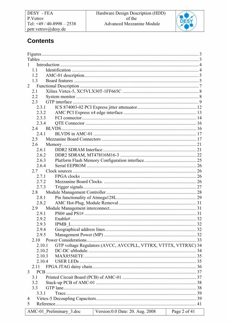
Figure 14 Mezzanine Board Clock The Table 7 is truth table of SY89547LMG multiplexer
Table 7 Truth table of SY89547L
IN0 IN1 IN2 IN3 SEL0 SEL1 Q0, Q1 Q0#, Q1# 0 X X X 0 0 0 1 1 X X X 0 0 1 0 X 0 X X 1 0 0 1 X 1 X X 1 0 1 0 X X 0 X 0 1 0 1 X X 1 X 0 1 1 0 X X X 0 1 1 0 1 X X X 1 1 1 1 0
2.7.3 Trigger signals The AMC-01 board has one external differential trigger input – IN_TRIGP and IN_TRIGN#. The FPGA receive external trigger from the FCI front panel connector – J7. The internal trigger signal can be generated by the FPGA and is used for debugging of the AMC-01 in standalone mode.
SY89547LMGAMC_CLK_A3_P
AMC_CLK_A3_N
ADC_CLK_EC_P
ADC_CLK_EC_N
IN_ACLK_P
IN_ACLK_N
FPGA_ACLK_P
FPGA_ACLK_N
S_CLK0
S_CLK1
From FPGA
From FCI connector
TCLKB from Edge connector
From jitter attenuator
IN0P
IN0N
IN1P
IN1N
IN2P
IN2N
IN3P
IN3N
SEL0
SEL1
Q0P ADC_MCLK_P
Q0N ADC_MCLK_N
ADC_MFCLK_P
ADC_MFCLK_N Q1P
Q1N
To Mezzanine Board
To FPGA

DESY - FEA P.Vetrov Tel: +49 / 40-8998 – 2538 [email protected]
Hardware Design Description (HDD) of the
Advanced Mezzanine Module
AMC-01_Preliminary_3.doc Version:0.0 Date: 20. Aug. 2008 Page 28 of 41
2.8 Module Management Controller The AMC-01 includes a Module Management Controller (MMC) based on the ATMEL ATMEGA128L-8MU microcontroller [12], which interfaces to the IPMI (Intelligent Platform Management Interface) bus. It provides a Serial Peripheral Interface (SPI) interfaces and is IPMI compliant. The MMC monitors and controls the subsystem, and performs remote diagnostics for many on-board functionality. Almost of all input/output signals of the MMC are connected to payload electronics via special buffer (U11) or a switch (U21). The MMC monitors the AMC’s sensors for system management events, such as over temperature, out-of-range voltages, etc. All interfaces to the MMC are shown on figure 15. Signals SEL_GTPN should be used only after ended of Payload configuration!
Figure 15 Interfaces to MMC
GA1
GA_PULLUP
SDA_L
SEL_1 SEL_0
GA0
FAILURE_LED
MMC_TDI
MMC_TMS MMC_TDO
FPGA_RST_MMC#
I2C_SDA
TDO
TCK TMS
TDI
PROGRAMM#
JTAG_CNT
EN_SWITCH
RUN_SS_DC
Reset
XTAL2
PA0 PA1 PA2 PA3 PA4 PA5 PA6 PA7
PGOOD PD0 PD1 PD2 PD3 PD4 PD5 PD6 PD7
PB0 PB1 PB2 PB3 PB4 PB5 PB6 PB7
PE0 PE1 PE2 PE3 PE4 PE5 PE6 PE7
MMC_RST
DONE
To FPGA JTAG Daisy chain
To FPGA
To FPGA
Select version of ISP PROM
Start/Stop DC-DC
From Power convertos
ENABLE#
Oscillator
Control Switch
I2C_SCL To SEEPROM And thermo Sensors
ATMEGA128L-8MU
SCL_L IPMB
MMC_TCK To MMC JTAG Connector
USD_LED
To Front Panel LEDs
To FPGA UART_RX UART_TX
HSWAP_LED
HSWAP_SW To Front Panel
IPMI GA2
MP
GND
GND
VCC
PC0 PC1 PC2 PC3 PC4 PC5 PC6 PC7
PF0 PF1 PF2 PF3 PF4 PF5 PF6 PF7
SEL_GTP1 SEL_GTP2 SEL_GTP3 SEL_GTP4
To FPGA GTP Control/Status
FUNC_LED
AVCCAREF
BEAD
MP
From FPGA
PS1# PS0#
From AMC Edge Connector
PG0PG1PG2PG3PG4
TEMP_INT1 From Thermo
SEL_JTAG_PLR JTAG Buffers
JTAG Buffers
GND
+12V ADC_1
XTAL1
DESY - FEA P.Vetrov Tel: +49 / 40-8998 – 2538 [email protected]
Hardware Design Description (HDD) of the
Advanced Mezzanine Module
AMC-01_Preliminary_3.doc Version:0.0 Date: 20. Aug. 2008 Page 29 of 41
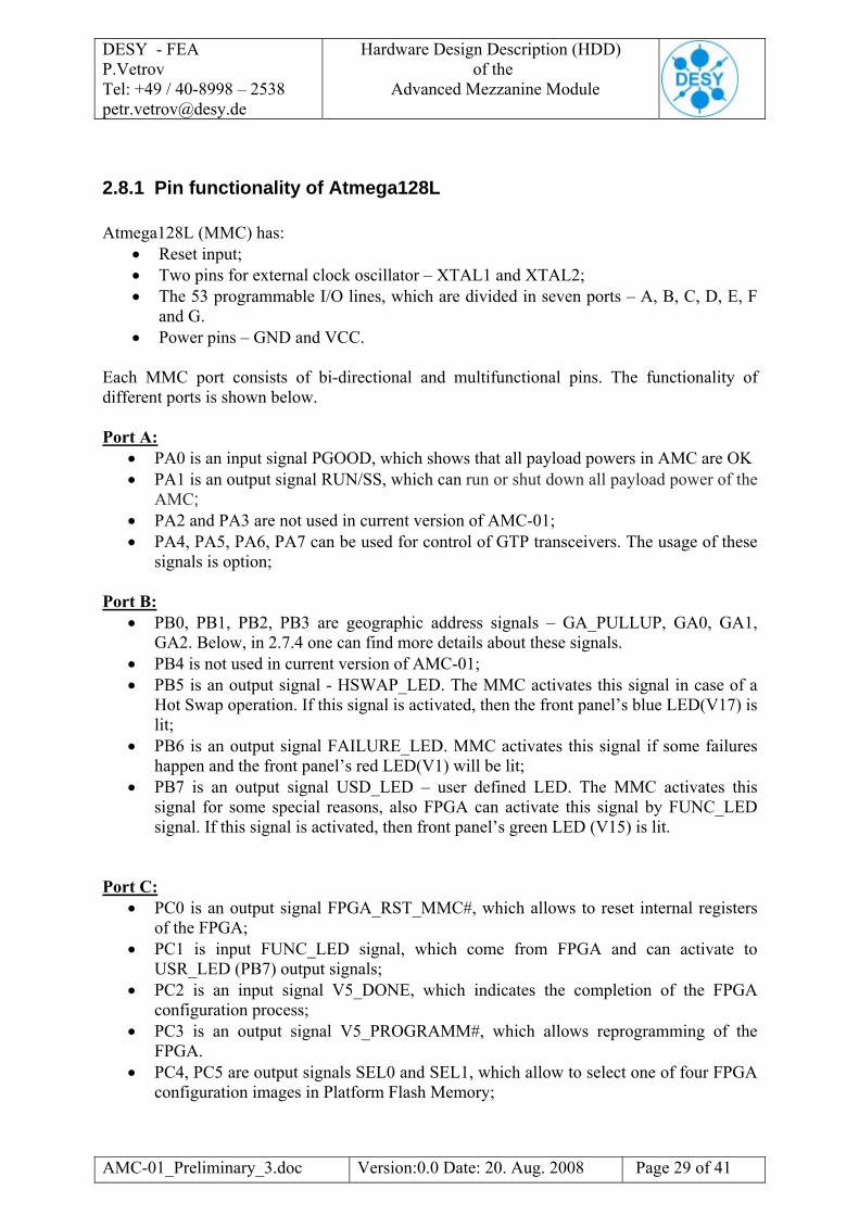
2.8.1 Pin functionality of Atmega128L Atmega128L (MMC) has:
• Reset input; • Two pins for external clock oscillator – XTAL1 and XTAL2; • The 53 programmable I/O lines, which are divided in seven ports – A, B, C, D, E, F
and G. • Power pins – GND and VCC.
Each MMC port consists of bi-directional and multifunctional pins. The functionality of different ports is shown below. Port A:
• PA0 is an input signal PGOOD, which shows that all payload powers in AMC are OK • PA1 is an output signal RUN/SS, which can run or shut down all payload power of the
AMC; • PA2 and PA3 are not used in current version of AMC-01; • PA4, PA5, PA6, PA7 can be used for control of GTP transceivers. The usage of these
signals is option; Port B:
• PB0, PB1, PB2, PB3 are geographic address signals – GA_PULLUP, GA0, GA1, GA2. Below, in 2.7.4 one can find more details about these signals.
• PB4 is not used in current version of AMC-01; • PB5 is an output signal - HSWAP_LED. The MMC activates this signal in case of a
Hot Swap operation. If this signal is activated, then the front panel’s blue LED(V17) is lit;
• PB6 is an output signal FAILURE_LED. MMC activates this signal if some failures happen and the front panel’s red LED(V1) will be lit;
• PB7 is an output signal USD_LED – user defined LED. The MMC activates this signal for some special reasons, also FPGA can activate this signal by FUNC_LED signal. If this signal is activated, then front panel’s green LED (V15) is lit.
Port C: • PC0 is an output signal FPGA_RST_MMC#, which allows to reset internal registers
of the FPGA; • PC1 is input FUNC_LED signal, which come from FPGA and can activate to
USR_LED (PB7) output signals; • PC2 is an input signal V5_DONE, which indicates the completion of the FPGA
configuration process; • PC3 is an output signal V5_PROGRAMM#, which allows reprogramming of the
FPGA. • PC4, PC5 are output signals SEL0 and SEL1, which allow to select one of four FPGA
configuration images in Platform Flash Memory;
DESY - FEA P.Vetrov Tel: +49 / 40-8998 – 2538 [email protected]
Hardware Design Description (HDD) of the
Advanced Mezzanine Module
AMC-01_Preliminary_3.doc Version:0.0 Date: 20. Aug. 2008 Page 30 of 41
• PC6 is an output signal EN_SWITCH, which enables or disables the low-Voltage 10-bit FET bus switch – U21. The usage of this switch allows to disconnect control signals of MMC from AMC payload parts, when payload power is not applied;
Port D:
• PD0, PD1 are two bidirectional open-drain lines, Serial Clock (SCL_L) and Serial
Data (SDA_L) for the I2C serial bus - IPMB, which connect the MMC to the back plane of the uTCA crate;
• PD2 is an input signal from the hot-swap switch – HAWAP_SW. The level of this signal defines the status of the AMC-01 – extraction or insertion;
• PD3 is not used in current version of AMC-01; • PD4, PD5 are two bidirectional open-drain lines, Serial Data (I2C_SCL) and
Serial Clock (I2C_SDA) for the I2C serial bus, which connect the digital thermometer (U18) and the FPGA thermo outputs, and the SEEPROM (U19) to the MMC;
• PD6 and PD7 are not used in current version of AMC-01.
Port E:
• PE0, PE1 are signals of the UART serial interface - UART_TX, UART_RX. MMC uses this interface for the connection to the FPGA;
• PE2 and PE3 are PS0# and PS1# signals, which detect the presence of an AMC-01 in the uTCA crate;
• PE4 is TEMP_INT1 input interrupt signal, which generated by thermometer (U18). If either measured temperature equals or exceeds the corresponding alarm threshold value, a TEMP_INT1 interrupt is asserted.
• PE5 is SEL_JTAG_PLR output signal, which allowed FPGA to control of Platform Flash JTAG;
• PE6 and PE7 are not used in current version of AMC-01. Port F:
• PF0 is internal ADC input, which is used for control of Payload Power (+12V); • PF1, PF2 and PF3 are not used in current version of AMC-01. • PF4, PF5, PF6, PF7 are input/output MMC JTAG signals - MMC_TCK,
MMC_TMS, MMC_TDO and MMC_TDI, which are connected to the MMC_JTAG connector – J9.
Port G:
• PG0, PG1, PG2, PG3 are input/output signals (TDI, TDO, TMS, and TCK) for the FPGA JTAG daisy chain. These signals are valid if the PG4 output is activated;
• PG4 is an output signal JTAG_CNT. When JTAG_CNT is at high level, the MMC becomes the JTAG controller for the FPGA JTAG daisy chain.

DESY - FEA P.Vetrov Tel: +49 / 40-8998 – 2538 [email protected]
Hardware Design Description (HDD) of the
Advanced Mezzanine Module
AMC-01_Preliminary_3.doc Version:0.0 Date: 20. Aug. 2008 Page 31 of 41
2.8.2 AMC Hot-Plug, Module Removal An operator can initiate a module removal by opening the module handle, which deactivates the hot-swap switch. When this switch opens or closes it sends a request via the MMC to the carrier for a hot swap extraction or insertion. Its function and behaviour is defined by the PICMG AMC.0 specification [1]. The hot swap blue LED (HSWAP_LED) indicates the state of the module during extraction and insertion.
2.9 Module Management interconnect Figure 16 shows the management interconnects between an AMC-01 board and back plane (ATCA Carrier) - IPMI. Note that active low signals are denoted with a trailing #. All logic levels are assumed +3V3 compatible unless otherwise noted.
Figure 16 Management interconnections
2.9.1 PS0# and PS1# The PS0# and PS1# pins are used to detect the presence of an AMC-01 in the uTCA crate. The PS0# and PS1# pins are last mate connections located on opposite ends of the edge connector – J4. These pins are used to compensate for any skew on the Module during insertion and provide confirmation that all pins of the AdvancedMC Edge Connector have mated (with a complementary role on extraction). The Back Plane connects PS0# to Logic Ground and pulls up PS1# to the 3.3V Management Power. The AMC-01 board connects PS1# to PS0# through a diode, providing a low voltage drop path from PS1# to PS0#. The
GA0
PS1#
PS0#
SDA_L
GA1
GA2
AMC Board
Back Plane
MP
SCL_L
ENABLE#

DESY - FEA P.Vetrov Tel: +49 / 40-8998 – 2538 [email protected]
Hardware Design Description (HDD) of the
Advanced Mezzanine Module
AMC-01_Preliminary_3.doc Version:0.0 Date: 20. Aug. 2008 Page 32 of 41
Back Plane (HUB) can detect the presence of an AMC-01 by an active PS1# signal. The AMC-01 can determine the insertion into a crate by the Carrier’s feedback of PS1# on ENABLE# as well as by a current flowing through the PS0# - PS1# connection.
2.9.2 Enable# The ENABLE# pin is an active low input to the AMC-01 pulled up on the AMC-01 to Management Power (MP). This signal is inverted on the board to create a RESET# signal toward the MMC. The negated state of this RESET# indicates to the MMC that the board is fully inserted and valid states exist on all inputs of the Module. The MMC is not allowed to read the GA inputs or use the IPMB-L while ENABLE# is inactive.
2.9.3 IPMB_L The Inter-Integrated Circuit bus (I2C) is a multi-master, 2-wire serial bus used as the basis for current IPMBs. IPMB_L is made up of clock (SCL_L) and data (SDA_L) signals. Some of the functions available on the AMC-01 board through the IPMB_L interface include:
• Monitoring of the FPGA and board temperatures; • Monitoring of the payload voltage rails (+3V3, +2V5, +1V8, +1V2, +1V); • Remote reset and shutdown of the board; • Monitoring of the ejector switches for the hot swap functionality; • Monitoring and event recording of critical errors; • Board power up and power down.
2.9.4 Geographical address lines Three Geographic Address (GA) pins are used to assign the address of an AMC on IPMB-L. Each of the GA pins can encode three different levels; they can be connected to Logic Ground, to Management Power, or left unconnected on the Back Plane to define the Geographic Address of the AMC-01. This scheme requires that the board be able to distinguish among three states. The state of the GA lines on the AMC-01 can be determined if each of the GA lines is connected to a MMC output (GA_PULLUP) through a resistor. The MMC drives GA_PULLUP low and reads the GA lines. The MMC then drives GA_PULLUP high and reads the GA lines. Any lines that change state between the two reads indicate an unconnected (U) pin.
2.9.5 Management Power (MP) The Module Management Power (MP) powers the AMC-01 management subsystem. It is ensured via requirements to the Back Plane (HUB) that Payload Power is only available the board if Management Power is available.
DESY - FEA P.Vetrov Tel: +49 / 40-8998 – 2538 [email protected]
Hardware Design Description (HDD) of the
Advanced Mezzanine Module
AMC-01_Preliminary_3.doc Version:0.0 Date: 20. Aug. 2008 Page 33 of 41
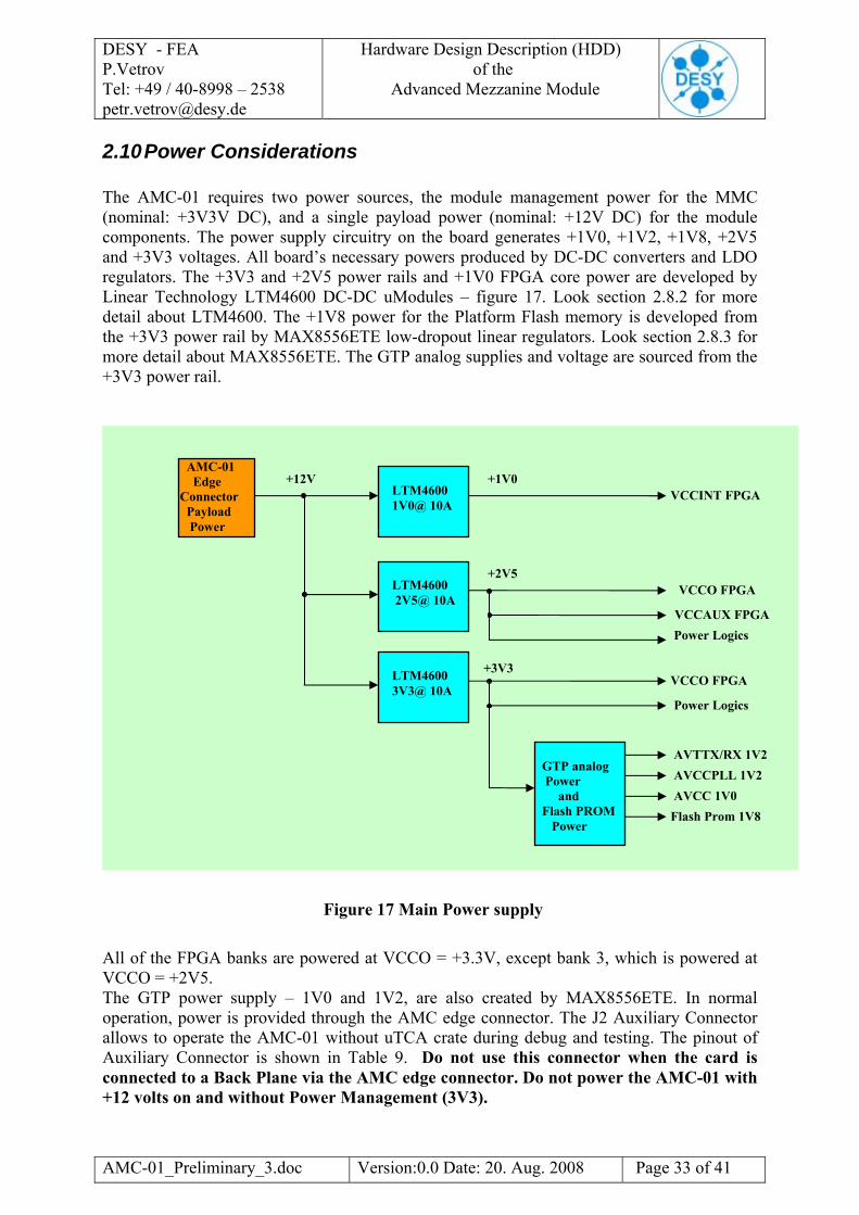
2.10 Power Considerations The AMC-01 requires two power sources, the module management power for the MMC (nominal: +3V3V DC), and a single payload power (nominal: +12V DC) for the module components. The power supply circuitry on the board generates +1V0, +1V2, +1V8, +2V5 and +3V3 voltages. All board’s necessary powers produced by DC-DC converters and LDO regulators. The +3V3 and +2V5 power rails and +1V0 FPGA core power are developed by Linear Technology LTM4600 DC-DC uModules – figure 17. Look section 2.8.2 for more detail about LTM4600. The +1V8 power for the Platform Flash memory is developed from the +3V3 power rail by MAX8556ETE low-dropout linear regulators. Look section 2.8.3 for more detail about MAX8556ETE. The GTP analog supplies and voltage are sourced from the +3V3 power rail.
Figure 17 Main Power supply
All of the FPGA banks are powered at VCCO = +3.3V, except bank 3, which is powered at VCCO = +2V5. The GTP power supply – 1V0 and 1V2, are also created by MAX8556ETE. In normal operation, power is provided through the AMC edge connector. The J2 Auxiliary Connector allows to operate the AMC-01 without uTCA crate during debug and testing. The pinout of Auxiliary Connector is shown in Table 9. Do not use this connector when the card is connected to a Back Plane via the AMC edge connector. Do not power the AMC-01 with +12 volts on and without Power Management (3V3).
AMC-01 Edge Connector Payload Power
LTM4600 1V0@ 10A
LTM4600 2V5@ 10A
LTM4600 3V3@ 10A
+3V3
+2V5
+1V0
VCCO FPGA
VCCINT FPGA
VCCO FPGA
VCCAUX FPGA
+12V
GTP analog Power and Flash PROM Power
AVTTX/RX 1V2 AVCCPLL 1V2 AVCC 1V0 Flash Prom 1V8
Power Logics
Power Logics

DESY - FEA P.Vetrov Tel: +49 / 40-8998 – 2538 [email protected]
Hardware Design Description (HDD) of the
Advanced Mezzanine Module
AMC-01_Preliminary_3.doc Version:0.0 Date: 20. Aug. 2008 Page 34 of 41
Table 8 Pinout of Auxiliary Connector - J2. PIN’S NUMBER
POWER & CONTROL PIN’S NUMBER
POWER & CONTROL
4 GND 1 GND 5 Management Power +3V3 2 Enable# for MMC 6 +12V 3 +12V
2.10.1 GTP voltage Regulators (AVCC, AVCCPLL, VTTRX, VTTTX, VTTRXC)
The AMC-01 board provides point-of-load regulation for the GTP supplies with three high precision, low dropout linear regulators from MAXIM. The MAX8556ETE LDO regulators provide up to 4 amps of current. The ultra-low input voltage requirement minimizes the voltage drop across the regulator saving the added cost of thermal solutions in most applications. The following figure 18 shows a high-level block diagram of the GTP power supplies
Figure 18 GTP powers
2.10.2 DC-DC uModule. The AMC-01 has three LTM4600 DC-DC uModules, which have next main features [13]:
• Complete Switch Mode Power Supply; • Wide Input Voltage Range: 4.5V to 20V; • 10A DC, 14A Peak Output Current;
MAX8556, AVTTX_1V2
MAX8556, AVCC_1V0
MAX8556, AVCCPLL_1V2
Power Supply Filter
Power Supply Filter
Power Supply Filter
+3V3
VITRTEX-5, XC5VLX30T, FF665
MGT112, MGT114, MGT116, MGT118: AVTTRX and AVTTX
Power Supply Filter
Power Supply Filter
Power Supply Filter
MGT112, MGT114, MGT116, MGT118: AVCC
MGT112, MGT114, MGT116, MGT118: AVCCPLL

DESY - FEA P.Vetrov Tel: +49 / 40-8998 – 2538 [email protected]
Hardware Design Description (HDD) of the
Advanced Mezzanine Module
AMC-01_Preliminary_3.doc Version:0.0 Date: 20. Aug. 2008 Page 35 of 41
• 0.6V to 5V Output Voltage; • 1.5% Output Voltage Regulation; • Ultrafast Transient Response; • Current Mode Control; • Pb-Free (e4) RoHS Compliant Package with Gold-Pad Finish • Up to 92% Efficiency; • Programmable Soft-Start; • Output Over voltage Protection; • Optional Short-Circuit Shutdown Timer; • Small Footprint, Low Profile (15mm x 15mm x 2.8mm) Surface Mount LGA
Package.
2.10.3 MAX8556ETE The MAX8556ETE Ultra-Low-input-Voltage low-dropout linear regulators operate from input voltages as low as 1.425V and are able to deliver up to 4A of continuous output current with a typical dropout voltage of only 100mV. The output voltage is adjustable from 0.5V to VIN - 0.2V. Main features of the MAX8556ETE [14] are:
• 1.425V to 3.6V Input Voltage Range; • Guaranteed 4A Output Current; • ±1% Output Accuracy Over Load/Line/Temperature; • 100mV Dropout at 4A Load (typ); • Built-in soft-start; • 800μA (typ) Operating Supply Current; • 150μA (max) Shutdown Supply Current; • Short-Circuit Current Foldback Protection; • Thermal-Overload Protection; • ±10% Power-OK; • Fast Transient Response; • 16-Pin Thin QFN 5mm x 5mm Package.
2.10.4 USER LEDs Nine discrete LEDS are installed on the board and are used to display the status of the internal logic and powers. These LEDs are attached as shown below in table 10.
Table 9 USER LEDs
LED REFERENCE
USAGE COLOUR REMARKS
V1 FPGA_HEART_BEAT Green - V2 FPGA_DONE Green - V5 MMC RESET RED - V6 Present Payload Power
+12V Green -
V7 Present Management Power +3V3
Green -

DESY - FEA P.Vetrov Tel: +49 / 40-8998 – 2538 [email protected]
Hardware Design Description (HDD) of the
Advanced Mezzanine Module
AMC-01_Preliminary_3.doc Version:0.0 Date: 20. Aug. 2008 Page 36 of 41
LED REFERENCE
USAGE COLOUR REMARKS
V8 MGT_ Power is wrong Green Must be altered to RED!
V9 FPGA_2V5 Power is wrong Green Must be altered to RED!
V10 FPGA_1V Power is wrong Green Must be altered to RED!
V11 FPGA_3V3 Power is wrong Green Must be altered to RED!
2.11 FPGA JTAG daisy chain The FPGA and Platform Flash memory can be configured through the JTAG port. The JTAG chain of the board is illustrated in figure19.
Figure 19 FPGA JTAG daisy chain The JTAG daisy chain can be controlled by signals from the uTCA edge connector or from the on board J3 JTAG connector. J3 should be used for programming the Platform PROM and FPGA in stand-alone mode. In addition, the MMC can also generate JTAG sequences, with blocking signals from J3 and the edge connector. At last, FPGA JTAG ACE (Advanced Configuration Environment) [15] Player can be implemented in FPGA. This software gives users great flexibility in creating in-system
TDO_PROM
TCK_PROM
TMS_PROM
TCK
TDO_F_P_M
AMC-00 Edge Connector
TDI_uTCA
TMS_uTCA
TCK_uTCA
TDO_uTCA
On Board J3 JTAG Connector
OE Tri State Buffer 2
TMS
TDI
MMC JTAG Controller JTAG CNT
TDI_PROM FPGA FPGA_EN JTAG
Tri State Buffer 3
Tri State Buffer 1 OE
Platform PROM
TDI_EDGE
TMS_EDGE
TCK_EDGE
TDO_EDGE
S_JTAG_PLR
S_JTAG_PLR OE

DESY - FEA P.Vetrov Tel: +49 / 40-8998 – 2538 [email protected]
Hardware Design Description (HDD) of the
Advanced Mezzanine Module
AMC-01_Preliminary_3.doc Version:0.0 Date: 20. Aug. 2008 Page 37 of 41
programming (ISP) solutions. The users can to revise existing designs, package the new bitstream programming files with the provided software utilities, and update the Platform PROM through the JTAG interface using the Embedded JTAG ACE Player.
3 PCB This chapter provides information about the PCB design of the AMC-01 board. The physical dimensions of the raw PCB are 180mm x 73.5mm. This 14-layer board has 8 signal layers, 3 GND layers and 3 power planes and uses FR4 material.
3.1 Printed Circuit Board (PCB) of AMC-01 The PCB consists of 14 physical layers: 8 signal layers, 3 GND layers and 3 power planes and uses FR4 material. The Plane Assignments are defined in table 11.
Table 10 Plane Assignment
LAYER LAYER DESCRIPTION PLANE TYPE 1 Signal_Top, and Power Area Fills: +1V, +1V8, +2V5,
+3V3, +12V, GND, Ref_RGND and VCC_CLKM_1 Positive
2 Plane_1: GND Positive 3 Signal_2 Positive 4 Split Plane_2: +1V, +2V5, +3V3 Positive 5 Signal_3, and Power Area Fills: +AVCC_114_U3,
AVCC_114_U4, AVTTTX_118_Y3 Positive
6 Plane_3: GND Positive 7 Signal_4 Positive 8 Plane_4: GND Positive 9 Signal_5, and Power Area Fills: AVCCPLL_114,
AVCCP_116_E3, AVTTRX_118_AA3 Positive
10 Split Plane_5: +1V8, +12V, VCC, 0.9V_REF Positive 11 Signal_6, and Power Area Fills: AVCCP_116_E4,
AVCC_118_AC4, AVTTTX_112_H3, AVTTTX_112_N3, REF_112
Positive
12 Signal_7, and Power Area Fills: AVCC_118_AC3, AVTTRX_112_P5, AVTTRX_112_J3, AVTTTX_114_P3, AVTTTX_114_W3, 3V3_4REF
Positive
13 Split Plane_6: +1V8, AVCCPLL_1V2, AVCC_1V0, AVTTX_1V2, VCC
Positive
14 Signal_Bottom, Split Plane: +1V8, +12V, AVCCPLL_116_F3, AVCCPLL_118_AD3, AVCCP_112_L3, AVCCP_112_L4, AVTTRX_114, AVTTRX_116_C3, AVTTTX_116_B3, AVTTTX_116_G3, AVTTTX_118_AE3, GND, GND_SCLK, VCCA_SCLK, VCC_SCLK, 0.9V_TT
Positive

DESY - FEA P.Vetrov Tel: +49 / 40-8998 – 2538 [email protected]
Hardware Design Description (HDD) of the
Advanced Mezzanine Module
AMC-01_Preliminary_3.doc Version:0.0 Date: 20. Aug. 2008 Page 38 of 41
3.2 Stack-up PCB of AMC-01 Figure 20 shows a stack-up diagram of the AMC-01 PCB
Figure 20 AMC-01 PCB Stack-up
3.3 GTP lane The RocketIO™ GTP Transceiver is a dual, simplex point-to-point serial differential low-voltage interconnection. Each lane consists of two pairs of differential signals: a transmit pair TXP/TXN, and a receive pair RXP/RXN. The PCI Express signals are 2.5 GHz with an embedded clock. The embedded clock simplifies routing rules by removing the length matching requirements between the differential pairs. Key requirements for the increased bit rate of PCI Express requires to minimize the interconnect loss and the jitter. This is achieved by target impedance and small tolerances. Thicker dielectrics and wider traces will minimize loss. A signal pair should avoid discontinuities in the reference plane, such as splits and voids. When a signal changes layers, the ground stitching vias should be placed close to the signal vias. A minimum of 1 to 3 stitching vias per pair of signals is recommended [16].
0.08 mm, Er = 4.7
0.02 mm, Top, Z0 = 50Ω, width = 0.12 mm
0.02 mm, 04_INR1, Z0 = 50Ω, width = 0.12
0.08 mm, Er = 4.70.02 mm, 02_PWR1
0.02 mm, 03_GND1 0.1 mm, Er = 4.7
0.13 mm, Er = 4.7
0.1 mm, Er = 4.7
0.1 mm, Er = 4.7
0.1 mm, Er = 4.7
0.1 mm, Er = 4.7
0.13 mm, Er = 4.7
0.13 mm, Er = 4.7
0.1 mm, Er = 4.7
0.08 mm, Er = 4.7
0.08 mm, Er = 4.7
0.02 mm, 05_INR2, Z0 = 50Ω, width = 0.12
0.02 mm, 07_INR3, Z0 = 50Ω, width = 0.12
0.02 mm, 08_INR4, Z0 = 50Ω, width = 0.12
0.02 mm, 10_INR5, Z0 = 50Ω, width = 0.12
0.02 mm, 11_INR6, Z0 = 50Ω, width = 0.12
0.02 mm, Bottom, Z0 = 50Ω, width = 0.12
0.02 mm, 06_GND2
0.02 mm, 09_GND3
0.02 mm, 12_PWR2
0.02 mm, 13_PWR3

DESY - FEA P.Vetrov Tel: +49 / 40-8998 – 2538 [email protected]
Hardware Design Description (HDD) of the
Advanced Mezzanine Module
AMC-01_Preliminary_3.doc Version:0.0 Date: 20. Aug. 2008 Page 39 of 41
3.3.1 Trace PCI Express link traces must maintain 100 Ω differential / 60 Ω single-ended impedance for 4-layer or 6-layer boards; and 85 Ω differential / 55 Ω single-ended impedance for 8-layer or 10-layer boards. Coupling of the intra-pair differential signals and increased spacing to neighbouring signals helps to minimize harmful crosstalk impacts and Electro-Magnetic Interference (EMI) effects. In the microstrip case, a differential trace should be 5 mils wide, with a 7 mil wide air gap spacing between the two traces of a pair. Any uncoupled sections whose intra-pair space exceeds 7 mils can be routed as a 7 mil wide trace, if the section is 100 mils or longer. In the stripline case, a differential trace should be 5 mils wide with a 5 mil wide gap between the two traces of a pair – figure 21. The spacing between pairs and to all non-PCI Express signals should be 20 mils or four times the dielectric height, whichever is greater. If the non-PCI Express signals have significantly higher voltage levels or edge rate than the PCI Express signal, the space should increase to 30 mils in order to avoid coupling.
Figure 21 Trace width and spacing For an add-in card, the trace length from the edge finger to the PCI Express pads should be limited to 4 inches (100 mm). The two traces of a pair should be symmetrically routed. The length difference between a differential pair should be limited to 5 mils maximum (0.127 mm). Length matching is required per segment, and any length added (typically a “serpentine” section) for the sake of matching a pair should be added near the location where the mismatch occurs. There is no length match requirement between transmit and receive pairs. The use of bends should be kept to a minimum, since a bend can introduce common mode noise into the system, which will affect the signal integrity and EMI of the differential pair.
4 Virtex-5 Decoupling Capacitors A simple PCB-decoupling network for each Virtex-5 LXT family device is listed in Table 12. Many of the devices require very few PCB ceramic capacitors because high frequency
7 7 5 5 5 5
TX TX 20mil
h
Microstrip
Stripline
5 5 5 5 5 5 TX TX
20mil
All dimension in mil. 5mil = 0.127 mm; 7mil = 0.18 mm; 20mil = 0.5 mm

DESY - FEA P.Vetrov Tel: +49 / 40-8998 – 2538 [email protected]
Hardware Design Description (HDD) of the
Advanced Mezzanine Module
AMC-01_Preliminary_3.doc Version:0.0 Date: 20. Aug. 2008 Page 40 of 41
ceramic capacitors are already present inside the device package (mounted on the substrate) [17]. Thus, fewer PCB decoupling capacitors are needed in Virtex-5 devices than in previous device families.
Table 11 Required PCB Capacitor Quantities per Device: LXT Devices
VCCINT VCCAUX
VCCO (PER I/O BANK)
TOTALPACKAGE DEVICE
330 uF
2.2uF
0.22uF
33 uF
2.2uF
0.22uF
47 uF
2.2 uF
0.22 uF
FF323 XC5VLX20T 1 3 6 1 1 3 1 2 4 50 FF324 XC5VLX30T 1 4 8 1 2 4 1 2 4 83 FF665 XC5VLX30T 1 - - 1 - - 1 - 11 FF665 XC5VLX50T 1 - - 1 - - 1 - 11 FF1136 XC5VLX50T 1 - - 1 - - - 2 The XC5VLX30T-FF665 and XC5VLX50T-FF665 can be used on AMC-01 board, because both of them are package/pins compatible and required PCB capacitor quantity is the same!

DESY - FEA P.Vetrov Tel: +49 / 40-8998 – 2538 [email protected]
Hardware Design Description (HDD) of the
Advanced Mezzanine Module
AMC-01_Preliminary_3.doc Version:0.0 Date: 20. Aug. 2008 Page 41 of 41
5 Reference 1. PICMG Advanced Mezzanine Card AMC.0 Specification R1.0 ECR-002 D0.8, April 28, 2006 2. Virtex-5 FPGA User Guide. UG190 (v4.2) May9, 2008. 3. Virtex-5 Integrated Endpoint Block for PCI Express Designs. UG 197 (v1.3) June 2, 2008 4. Virtex-5 RocketIO GTP Transceiver User Guide. UG196 (v1.6) February 11, 2008 5. Virtex-5 FPGA Packaging and Pinout Specification. UG195 (v4.3) June 18, 2008 6. Virtex-5 FPGA System Monitor. UG192 (v1.4) April 21, 2008 7. PCI Express Jitter Attenuator. ICS874003-DG REV.A JUNE 13, 2007 8. MT47H16M16 – 4 Meg x 16 x 4 banks. Micron. 09005aef80b12a05 256MbDDR2_1.fm - Rev. J 11/05 EN 9. High-Performance DDR2 SDRAM Interface in Virtex-5 Devices. XAPP858 (v2.1) May 8, 2008 10. Platform Flash PROM User Guide.UG161 (v1.3) June 18, 2008 11. Platform Flash In-System Programmable Configuration PROMs. DS123 (v2.15) 12. 8-bit Microcontroller with 32K Bytes In-System Programmable Flash. 2503J-AVR-10/06 13. LTM4600 - 10A High Efficiency DC/DC uModule. Linear Technology Corporation. 14. 4A Ultra-Low-Input-Voltage LDO Regulators. 19-3257; Rev 0; 4/04. 15. Embedded JTAG ACE Player. XAPP424 16. PCI Express PHY PCB Layout Guideline. Rev. 01 — 30 April 2005. AN1037.Philips 17. Virtex-5 PCB Designer’s Guide. UG203 (v1.2) May 19, 2008