hands-on lcd color monitor troubleshooting tech schoolslot-tech.com/interesting_stuff/a collection...
TRANSCRIPT

Hands-on LCD Color Monitor
Troubleshooting Tech School

Hands-On LCD Color Monitor Tech-School Objectives This hands-on Sencore Tech School is designed to teach you the functional stages and operational theory of LCD color monitors. It introduces effective troubleshooting procedures and has you apply these procedures on an actual LCD color monitor using Sencore test instruments. The objectives are threefold: # 1 Tech - Theory
Study of the functional parts and operational theory of the stages that comprise a color LCD Monitor. Upon completion of the Tech-School a technician should understand LCD color monitors and be able to troubleshoot them more effectively.
#2 Tech-Procedure:
Introduction of effective troubleshooting procedures to isolate the defect. Hands-on troubleshooting of problems on an actual LCD color monitor. Upon completion of the Tech-School a technician should be able to perform troubleshooting steps to isolate a defect.
#3 Tech-Tools:
Introduce measurements and apply test equipment to analyze functional parts of an LCD color monitor. Apply test equipment to test critical functional sections and components. Upon completion of the Tech-School a technician should be familiar with analyzing measurements and the use of test equipment needed to performance test and analyze LCD color monitors.
For over 50 years Sencore has been dedicated to the goal of making you more successful in electronic servicing.
Learning new concepts helps you save hundreds of troubleshooting hours and saves thousands of dollars.

1
LCD Color Monitor Hands-On Tech School - Agenda
A. Introduction/Tech School Objectives.............................................................. inside front cover B. Equipment Familiarization.........................................................................................................2
1. LCD Color Monitor Tech-Trainer ...............................................................................2 2. Resistor Dummy Load Familiarization........................................................................3 3. PR570 ..........................................................................................................................4 4. SC3100 ........................................................................................................................5 5. PSL60 ..........................................................................................................................6 6. VP401 ..........................................................................................................................7
C. LCD Color Monitors ..................................................................................................................8
1. LCD Color Monitor Introduction.................................................................................8 2. LCD Display Resolution..............................................................................................9 3. Understanding LCD Display Technology..................................................................10 4. LCD Color Display vs. CRT Displays.......................................................................17 5. Testing LCD Color Monitor for Bad Pixels...............................................................19 6. Introduction to Digital Signal Processing ..................................................................20 7. Analyzing Differential Signals...................................................................................22 8. LCD Color Monitor Trainer User Controls/OSD Menus...........................................24 9. LCD Color Monitor Circuit Boards/Modules ............................................................26 10. LCD Color Monitor Block Diagram..........................................................................27 11. VGA Input ................................................................................................................29 12. The New Digital Video Interface – DVI....................................................................31 13. Display Data Channel (DDC) ....................................................................................36 14. Testing the AC Power Adapter or SMPS...................................................................38 15. Display Power Management Signaling......................................................................39
D. LCD Color Monitor Troubleshooting ......................................................................................41
1. Main Signal Processor & Control Circuits.................................................................41 2. Main Signal Processing/Control Board Power Supplies............................................44 3. Understanding the LVDS Interface............................................................................47 4. The LCD Panel ..........................................................................................................56 5. LCD Panel Protection ................................................................................................60 6. LCD Display Backlight Introduction & System Overview........................................61 7. Cold Cathode Fluorescent Lamp (CCFL) ..................................................................62 8. Backlight Inverter Power Supplies ............................................................................63 9. LCD Color Monitor Troubleshooting ........................................................................65
E. Backlight Inverter Power Supply Theory.................................................................................67
1. Backlight Inverter Oscillator......................................................................................68 2. Controlling CCFL Brightness ....................................................................................70 3. CCFL Current Sensing...............................................................................................72 4. Troubleshooting Backlight Inverter Power Supplies Symptoms ...............................73 5. Performance Testing Backlight Inverter Power Supplies Outputs.............................73 6. Kristel Backlight Inverter Power Supply Theory.......................................................74 7. KIA494 Controller IC................................................................................................75 8. Testing Luminance Uniformity .................................................................................77 9. Luminance (Y) Measurements – ColorPro ................................................................78 10. Backlight Inverter Power Supply Troubleshooting\...................................................81 11. Powering/Testing Inverter Power Supplies with a Bench DC Power Supply............85 12. Finding Replacement CCFLs or Inverter Power Supplies .........................................87 13. Replacing CCFFs or CCFL Assemblies ....................................................................87
F. LCD Color Monitor Alignment................................................................................................88
1. LCD Color Display User Control Adjustments .........................................................88 2. LCD Color Monitor Color Adjustment......................................................................91 3. ColorPro Familiarization ...........................................................................................95

2
Equipment Familiarization – LCD Color Monitor Trainer The Sencore LCD color monitor trainer is typical of the circuits and circuit boards found in LCD computer monitor and gaming LCD monitors.
The LCD Color Monitor Trainer is simply an LCD color monitor with its circuit boards and LCD panel mounted for convenience of discussion, measurement, and analysis. The trainer consists of the LCD Panel (center), Backlight Inverter Power Supply (right), Main signal processor board (center left), User control panel (bottom left), Trouble-switch panel (lower left) and AC Power Adapter (not pictured). The LCD Trainer contains test panels above its printed circuit boards. The test panels contain a block/circuit diagram of the circuitry contained on the circuit board below it. Test points are mounted within the block diagram and wired to the associated circuit points on the circuit board below. The test points make finding and measuring circuit points convenient, fast and safe. The LCD Color Monitor Trainer is powered by an AC Power Adapter. The Power Adapter plugs into the DC Input receptacle at the top left side of the Main Signal Processor Board. For all course activities the LCD Trainer’s AC Power Adapter is plugged into the Isolated Output Receptacle of the PR570. The Main Signal Processor board, located on the left center, has two signal inputs. The inputs include a VGA Input and DVI Input. A signal generator is used during all course activities to test and apply signals to these inputs. The LCD Color Monitor Trainer is unique as it permits many problems to be switched into the circuits of the trainer. The problems create many different symptoms typical of those a service technician encounters when troubleshooting LCD color monitors. Course activities include a block diagram and troubleshooting flow chart that is used to isolate the problem. Suggested Activity: LCD Color Monitor Trainer Familiarization
CAUTION: Inverter Power Supply Outputs are high frequency, high AC voltage outputs. Take care not to come into contact with these circuit test points.

3
Resistor Dummy Load Familiarization The Resistor Dummy Load consists of five 56K ohm power resistors connected in series. The load connection points are labeled A through E. The A connection is used as a common reference point (black) and is intended for connection to the CCFL ground return on the backlight inverter power supply. Connection points B through E offer increasing amounts of load resistance, in respect to A, and are intended for connection to one of the backlight inverter supply outputs. A resistor dummy load pack is used for troubleshooting the backlight inverter power supply. The Resistor Dummy Load is used to substitute for a single CCFL bulb on any one of the outputs on a multiple output backlight inverter supply. Two Resistor Dummy Load modules are supplied for use during the course activities. This enables CCFL substitution of two outputs on one side of the backlight inverter supply or one output on both sides of the backlight inverter supply simultaneously. With the proper substitution of inverter outputs, the supply can be tested and operated independent of the CCFL bulbs. The Resistor Dummy Load modules are sized for convenient placement near the top or bottom of the inverter power supply on the Sencore LCD Color Monitor Trainer. The rubber feet minimize slipping on the trainer board. The Resistor Dummy Load modules may be positioned so the connection terminals are close to the inverter supply either at the top or bottom. The labels can always be read if the terminals are positioned at the top or at the bottom of the board. To substitute a CCFL output with the Resistor Dummy Load, always be sure to remove power to the LCD monitor when unplugging connectors and making clip connections. With the power off, remove the plug from the inverter power supply that connects the CCFL bulb wires to the inverter supply. Connect a test clip lead from connection A on the Resistor Dummy Load to the ground return point for all the CCFL bulbs to the inverter supply. Connect a second lead from connection point B, C, D, or E, to the inverter output in which the plug was removed. Apply power to the LCD Color Monitor and test the inverter power supply output. You may use a second Resistor Dummy Load to substitute another output in a similar manner. Suggested Activity: Resistor Dummy Load Familiarization

4
Equipment Familiarization - PR570
To insure safe troubleshooting always plug the AC cord of the electronic system being serviced into an isolation transformer. The isolation transformer electrically isolates the AC line’s HOT side of the plug eliminating voltage differences and current that may result between grounds. The PR570 POWERITE contains an isolation transformer. Safe and effective servicing of electronic systems and power supplies depends on having a proper AC voltage. The PR570 checks the AC outlets hot to safety ground and hot to neutral voltage potentials to detect improper AC voltage or outlet wiring. A variable AC voltage to the electronic system is helpful when isolating power supply shorts, regulation defects, and other symptoms. The PR570 provides a variable AC voltage to the Isolated Output Jack and to the system being serviced. The CURRENT/POWER display reads the current or power to the Isolated Output jack and electronic system being serviced. Turn the CURRENT/POWER Switch to “CURRENT” to apply AC voltage to the Isolated Output Jack. A red light turns on beside the Isolated Output Jack. The current flowing to the electronic system is displayed. Switch to “POWER” to read the output power. A variable current trip feature acts as an output circuit breaker to limit the amount of current flowing to the electronic system from the PR570. The current trip point is adjustable from 0 to 4 amps with the TRIP SET Control. All AC operated electronic systems should be tested to be sure they do not pose a shock hazard to users after the product has been serviced. After the repair a Safety Leakage Current Test should be performed. The PR570 provides a Safety Leakage Test. Suggested Activity: PR570 Familiarization

5
Equipment Familiarization – SC3100
Troubleshooting electronic systems, such as LCD Color Monitors, requires making circuit voltage and waveform measurements. The Sencore SC3100 measures circuit voltages, analyzes waveforms and makes circuit checks faster than any other method and with less chance of measurement error. The SC3100 has no menus, multiple functions, complicated setups, or confusing on-screen readouts; just push-button ease, high performance waveform analyzing and digital readout accuracy. Auto-tracking push-button channel tests provide DCV, VPP and frequency measurements. Just attach the ground clip to ground, touch the probe tip to the test point and push the DCV push-button to measure the DC voltage. SC3100 control settings cannot cause an improper DCV reading. Push the VPP (volts peak-to-peak) pushbutton to measure the channel VPP. Readings to over 2000VPP can be safely measured to accommodate output measurements of the LCD monitor’s backlight inverter power supplies. If you are not sure were to set the Volts/Div control simply view the VPP readout of the channel. Flashing display digits indicate a higher setting of the Volts/Div Control is required. Measuring a waveform frequency is a simple as locking in the waveform trace on the screen and pushing the frequency push-button. Auto-ranged attenuator and time-base provide fast hands-off analyzing of non-complex waveforms. Setting the Volts/Div control to “AUTO” sets the SC3100 to select a position based upon its channel VPP measurement. Setting the TIME/DIV control sets the SC3100 to select a position automatically based upon the channel frequency readout. Delta measurements analyze any part of a waveform to determine the VPP, time duration, or frequency of a portion of the waveform, or the absolute DCV of a selected point along the waveform (Delta DC). Push the desired delta test push-button, highlight the section of the waveform to be analyzed with the DELTA MARKER Controls and read the measurement value in the display. Suggested Activity: SC3100 Familiarization

6
Equipment Familiarization – PSL60
The LCD Color Monitor training course uses an electronic load to serve as the circuitry normally powered by a DC power supply and to teach troubleshooting methods. While troubleshooting, the PSL60 quickly and accurately substitutes for the power supply’s load circuitry to determine if the problem is in the power supply or load circuits. An electronically adjustable load permits easy diagnoses of power supply regulation, current limiting, over-voltage shutdown and other power supply stage defects. The equivalent resistance of the electronic load is controlled electronically from approximately 0.5 ohms to 20,000 ohms and can dissipate up to 60 watts of power. Electronic control circuitry varies the load resistance by setting the level of current that is permitted to flow. Setting a load current rather than resistance provides and easier reference when working with a wide range of voltages and power settings. Control of the electronic load is divided up into ranges of voltages and power. Multiple voltage ranges enable the PSL60 to provide numerous current steps (load resistor values) for each potential DC power supply voltage to be tested. Multiple power ranges provide even finer current steps and reduce the chance of overloading DC supplies designed for low power applications. Metering circuits measure the input voltage to the electronic load, load current and load power. Measurements are displayed simultaneously in the digital display for ease in setting the electronic load and testing DC power supplies. Suggested Activity: PSL60 Familiarization
7
Equipment Familiarization – VP401
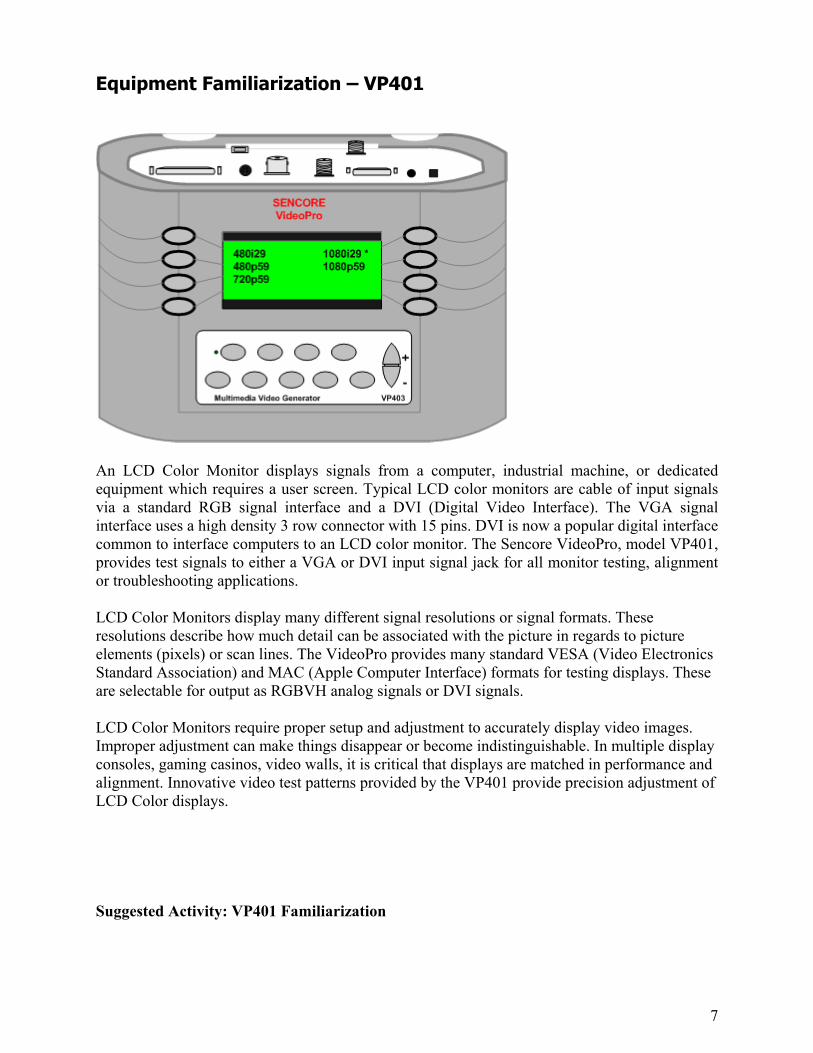
An LCD Color Monitor displays signals from a computer, industrial machine, or dedicated equipment which requires a user screen. Typical LCD color monitors are cable of input signals via a standard RGB signal interface and a DVI (Digital Video Interface). The VGA signal interface uses a high density 3 row connector with 15 pins. DVI is now a popular digital interface common to interface computers to an LCD color monitor. The Sencore VideoPro, model VP401, provides test signals to either a VGA or DVI input signal jack for all monitor testing, alignment or troubleshooting applications. LCD Color Monitors display many different signal resolutions or signal formats. These resolutions describe how much detail can be associated with the picture in regards to picture elements (pixels) or scan lines. The VideoPro provides many standard VESA (Video Electronics Standard Association) and MAC (Apple Computer Interface) formats for testing displays. These are selectable for output as RGBVH analog signals or DVI signals. LCD Color Monitors require proper setup and adjustment to accurately display video images. Improper adjustment can make things disappear or become indistinguishable. In multiple display consoles, gaming casinos, video walls, it is critical that displays are matched in performance and alignment. Innovative video test patterns provided by the VP401 provide precision adjustment of LCD Color displays. Suggested Activity: VP401 Familiarization

8
LCD (Liquid Crystal Display) Color Monitor Introduction The LCD “flat panel” display is a display newcomer. LCD technology displays originated in military displays in the 1960s. Commercially LCD displays became available in watches and calculators in the early 1970s. Since its advent in 1971 as a display medium, LCDs have moved into a variety of fields, including miniature televisions, digital still and video cameras and monitors. Today many believe that the LCD is the likely technology to replace the CRT monitor. It certainly has a good start and holds an apparently unassailable position in notebook and handheld PCs. Early LCD computer displays were clumsy, monochrome boxes offering limited gray scale graduations, poor saturated colors, narrow viewing angles and, slow response. The current state-of-the-art LCD panels are evolving rapidly and approach or exceed CRT performance in these categories. Additional improvements are forth coming. LCD Color Displays, when compared to other display technologies are thin and lightweight and run on low voltage power supplies and drive signals. Low voltage drive signals enable LSI (Large Scale Integration) circuitry to drive the display directly. The LCD display panel consumes very little power making portable, battery operation possible. Manufacturing techniques have reduced the cost of the displays lowering consumer pricing. According to research firm iSuppli, worldwide revenue for LCD panels is expected to reach $47 billion in 2004, up 32% from 2003. In 2003, the worldwide LCD market rose 27.9% to $35.7 billion. Market research firm Display Search predicts LCD monitor growth in 2004 to 14 million units worldwide and will grow to more than 46 million by 2005. LCD Color Monitor prices continue to fall fueling increasing sales.

9
LCD Display Resolutions CRT Monitors are capable of displaying a range of input signal resolutions without modification. In a CRT the scanning circuits are made to change rates or frequencies in accordance with the input signal format to display it. A VGA input signal (640x480) is scanned on the screen at a horizontal scanning frequency or 31.5 kHz. A 1280x1024 input signal is scanned onto the full screen at a much higher horizontal scanning frequency. In this manner the input signal resolution determines the displayed resolution. An LCD panel has a fixed number of liquid crystal cells and can display only one resolution at full-screen size using one cell per pixel. This is the LCD panel’s native resolution. Lower resolutions could be displayed without changing the resolution by using only a portion of the screen. For example, a 1024x768 panel can be displayed at a resolution of 640x480 by using only 66% of the screen. As this would not be acceptable by most users, modern LCD monitors are capable of rescaling lower-resolution images to the LCD’s native display resolution and displaying it full screen. This is accomplished by electronic sampling of the image and a scaling processor. A limited number of input signal resolution formats can be scaled and displayed at the LCD’s display’s native resolution. Unlike CRT monitors, the diagonal measurement of an LCD is the same as its viewable area, so there's no loss of the traditional inch or so behind the monitor's faceplate or bezel. The combination makes any LCD a match for a CRT 2 to 3 inches larger: By early 1999 a number of leading manufacturers had 18.1 inch TFT models on the market capable of a native resolution of 1280x1024. Native resolutions for LCD Display panels.
VGA: 640 x 480 SVGA: 800 x 600 XGA: 1024 x 768 SXGA: 1280 x 1024 SXGA-Wide: 1600 x 1024 UXGA: 1600 x 1200 HDTV: 1920 x 1080 UXGA-Wide: 1920 x 1200 QXGA: 2056 x 1536

10
Understanding LCD Display Technology For many years CRTs have been the standard display device. The development of the first LCD (liquid crystal display) by RCA Laboratories in 1968 ushered in a new era of displays. Since then, LCDs have been incorporated into all types of digital devices from small watches and calculators to video displays and projection televisions. Early LCD displays suffered from limited gray scale graduations, poorly saturated colors, narrow viewing angles, and slow response times. Today’s LCD panels have greatly improved, and are beginning to rival CRTs in most performance areas. But, in terms of size, weight and power consumption, LCD displays are far superior. This article introduces you to LCD technology and LCD displays. How LCD panels work The basic function of the LCD is a light "valve", either blocking light or allowing light to pass through. LCD video displays are “transmissive” meaning that an LCD is an active filter that works by varying the amount of light (from a fluorescent light source called the backlight) that is able to pass through to the viewing screen. An LCD display is really a large collection of thousands of these small filters called liquid crystal cells. Arranged together in rows and columns, these cells form an LC panel. Cells are combined into groups of three containing a uniquely addressable “red”, “green” and “blue” cell. These cells or subpixels, working together, create one pixel or picture element. A complete LCD display contains thousands of these tiny liquid crystal panels or cells. Its native resolution refers to the resolution that the LCD monitor is designed for (i.e. 800 x 600 or 1024 x 768) and is determined by the actual number of liquid crystal cells in the display. To produce color, every pixel location in an LCD display consists of three LC cells - one each for red, green, and blue. Each LC cell, or subpixel, can be individually addressed with a control voltage. This means, for example, that a 15" 1,024 x 768 video display contains 2,359,296 subpixels (1,024 x 768 x 3).
A CRT monitor can easily display a variety of input resolutions without any loss in image quality; it is capable of producing a white or color dot at virtually any location on the screen. Fixed pixel displays such as LCD displays (all display types except CRTs are fixed pixel displays) can provide the best image only in their native resolution. While you can input an image having a
resolution other than the display native resolution, the display can only reproduce a white or colored dot at the fixed physical pixel locations. To view an image at some other resolution, it needs to be scaled up or down in order to fill the screen. Fixed pixel displays are sometimes called "addressable displays" because each pixel can be addressed directly.
Fixed pixel displays can provide the best image
only in their native resolution.
11
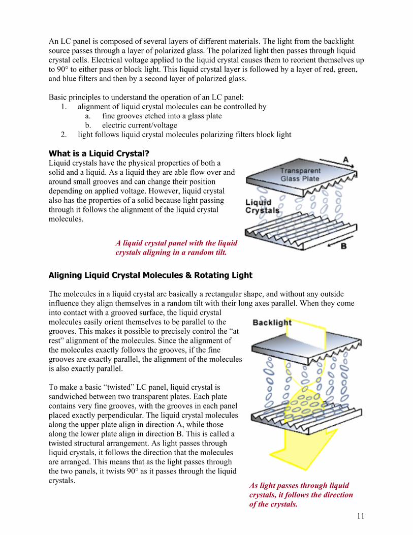
An LC panel is composed of several layers of different materials. The light from the backlight source passes through a layer of polarized glass. The polarized light then passes through liquid crystal cells. Electrical voltage applied to the liquid crystal causes them to reorient themselves up to 90° to either pass or block light. This liquid crystal layer is followed by a layer of red, green, and blue filters and then by a second layer of polarized glass. Basic principles to understand the operation of an LC panel:
1. alignment of liquid crystal molecules can be controlled by a. fine grooves etched into a glass plate b. electric current/voltage
2. light follows liquid crystal molecules polarizing filters block light What is a Liquid Crystal? Liquid crystals have the physical properties of both a solid and a liquid. As a liquid they are able flow over and around small grooves and can change their position depending on applied voltage. However, liquid crystal also has the properties of a solid because light passing through it follows the alignment of the liquid crystal molecules. Aligning Liquid Crystal Molecules & Rotating Light The molecules in a liquid crystal are basically a rectangular shape, and without any outside influence they align themselves in a random tilt with their long axes parallel. When they come into contact with a grooved surface, the liquid crystal molecules easily orient themselves to be parallel to the grooves. This makes it possible to precisely control the “at rest” alignment of the molecules. Since the alignment of the molecules exactly follows the grooves, if the fine grooves are exactly parallel, the alignment of the molecules is also exactly parallel. To make a basic “twisted” LC panel, liquid crystal is sandwiched between two transparent plates. Each plate contains very fine grooves, with the grooves in each panel placed exactly perpendicular. The liquid crystal molecules along the upper plate align in direction A, while those along the lower plate align in direction B. This is called a twisted structural arrangement. As light passes through liquid crystals, it follows the direction that the molecules are arranged. This means that as the light passes through the two panels, it twists 90° as it passes through the liquid crystals.
A liquid crystal panel with the liquid crystals aligning in a random tilt.
As light passes through liquid crystals, it follows the direction of the crystals.

12
An important key to the operation of an LCD panel is that liquid crystal molecules can be easily rearranged by applying an external voltage to them. As voltage is applied between the two grooved panels, the liquid crystal molecules begin to rearrange themselves with the electric field. In this illustration they align vertically or stand up out of the grooves. As the voltage increases, the molecules rotate, until they are standing completely upward. Remember that as light passes through liquid crystal, it follows the direction that the molecules are arranged. So, with full voltage applied the light passes through the panels following the arrangement of the molecules without being rotated 90°. At lower voltages the molecules are not all fully aligned, so some light is directed at different directions. Blocking Light with Polarizing Filters Natural light travels in waves that are oriented at random angles. This is why an object has the same color and brightness when viewed from different angles (unless it has a shadow or other lighting differences). A polarizing filter is simply a set of extremely closely spaced parallel lines. These lines allow only the light waves that are parallel to them to pass through – light from all other directions is blocked. (This is how polarized sunglasses work.) If you were to lay two polarizing filters on top of each other with the lines in one parallel to the lines in the other, direct light would pass through each, with little loss. However, as you begin to rotate one filter, more and more light is blocked because only the light waves that have the proper orientation to both filters can get through. When you have rotated the filter so that the lines in one are perpendicular to the lines in the other, all light will be blocked. This figure illustrates how two polarizing filters can be used to block light. In both the left and right drawing, light is applied to the top of the filter pair. The incoming light has waves oriented at all directions, but for simplicity, only two orientations, “a” and “b” are shown. In the left diagram, the polarizing filters are oriented so that their “A” filter lines are parallel. Incoming light waves that have orientation “A” are able to pass through both the first and second filter, but light waves that are “B” orientation are blocked by both filters. In the right drawing the two polarizing filters are oriented so the filter lines in one
With full voltage applied, the light passes through the panels without being rotated 90º.
Polarizing filters allow light waves that are parallel to them to pass through.

13
are perpendicular to the lines in the other. Again, light waves that are “A” orientation pass through the top filter, and “B” oriented waves are blocked. But in this case, when the “A” oriented waves reach the bottom polarizing filter, they are the wrong orientation compared to the filter lines, and they are unable to pass through. The result is: no light gets through the polarizing filters. Controlling Light with an LCD Panel You cannot physically rotate polarizing filters to pass or block light in a video display, but we can use the properties of liquid crystal to rotate light. Let’s add some liquid crystal between the two polarizing filters, as illustrated in figure 5. In both of these illustrations the polarizing filters are oriented perpendicular, which as we saw in the previous figure, prevents all incoming light from getting through. Also notice that a liquid crystal panel is inserted between the polarizing filters. This panel has a twisted structural arrangement (the molecules along the top plate are rotated 90° from those along the bottom plate). Figure 5 left, illustrates how the liquid crystal allows light to pass through the polarizing filters. Light waves that have an “A” orientation pass through the 1st (top) filter. These light waves are then rotated 90° by the liquid crystal in the twisted structural arrangement. Notice that this re-orientates the light waves so that they are now properly aligned to pass through the 2nd (bottom) polarizing filter. In Figure 5 right, a voltage is applied to the liquid crystal, causing the molecules to re-align themselves vertically. Again light waves that have an “A” orientation pass through the 1st filter, but this time they travel straight through the liquid crystal without being reoriented. Because they are perpendicular to the 2nd polarizing filter, they are blocked and no light makes it through the liquid crystal panel. Note that varying the amount of voltage applied to the liquid crystal determines how much it twists. With a lesser voltage applied the molecules don’t fully rotate, and some light waves will be able to pass through the bottom polarizing filter. By changing the voltage in very small increments, LCDs can create a gray scale (or different intensities of R, G or B light). Most displays today offer 256 levels of brightness. LC Cell Construction The complete structure of a liquid crystal cell is illustrated in Figure 6. If you were to look at this structure, it resembles a sheet of glass in terms of transparency and thickness, but it is much more complex. This illustration shows the basic structure of a single liquid crystal cell. 1. Backlight: light source, usually several fluorescent tubes, and a diffuser. 2. Polarizing filter: two polarizing filters establish the orientation of the light waves that are able
to pass through the LC cell.
Voltage applied to the liquid crystal causes the molecules to realign vertically.

14
3. Glass substrate: provides mechanical support for the cell.
4. Transparent electrodes: conduct the control voltage to the liquid crystal.
5. Alignment layer: contains the fine grooves that align the liquid crystal molecules in a fixed direction. In dual scan screens, the orientation varies between 90° and 270°.
6. Liquid crystal: molecules realign to applied voltage, light waves follow molecules.
7. Spacer: maintains uniform spacing between glass plates.
8. Color filter: determines what color of light is transmitted by the LC cell.
Addressing the Pixels To produce an image on the display, each of the subpixels must be made to turn on and off at the correct time. In addition, to produce shades of gray and different colors, the voltage applied to each LC cell must be variable. Since it is physically impossible to have a unique wire going to each of the 2.3 million pixels, another method of addressing the pixels is needed - LCD pixels are controlled using a matrix. To understand how an LCD matrix works, consider the small 4 x 4 checkerboard illustrated in figure 14.7, which has a light bulb in each square. The bulbs in each horizontal row are connected together to a common wire, giving us 4 separate rows of wire. At the end of each wire attach a terminal so that we can connect a battery. Likewise, connect the bulbs in each vertical column to a common wire, for a total of 4 column wires. Now connect a battery between one of the row wires and one of the
column wires – notice that only the bulb that corresponds to the intersection of the row and column wire is lit. By connecting to different combinations of row and column wires, we can individually turn on each light bulb. The matrix addressing in an LCD works just like this, except on a much larger grid. In a color LCD display, the intersection of each grid wire corresponds to a single LC cell, or subpixel (remember a 1,024 x 768 display contains 2,359,296 subpixels). The intersecting grid of horizontal and vertical conductors are etched onto the glass plates or substrates of the LC cell – the row conductors are etched onto one plate and the column conductors are etched on the other plate. These conductors are made of a transparent material, such as indium-tin oxide. Large scale integrated circuits (LSICs) control the timing of the signal voltage that is applied to each individual LC cell, one cell at a time. Connections to the transparent conductors are made through bonding pads that are located at the ends of the rows and columns on the LCD assembly.
A liquid crystal cell resembles a sheet of glass, but is much more complex.
Connecting a battery to different combinations of row and column wires turns on each light bulb individually.

15
Depending on the applied voltage, the LC cell can either pass or block all light, or partially pass light. There are two different ways of applying the drive voltages to an LCD screen using this matrixing process: passive matrix and active matrix. Simple displays, such as those used in calculators or clocks, only need to address pre-defined patterns. These displays use segment drive where each pattern segment is addressed directly.
Passive Matrix LCD (PMLCDs) Passive matrix is the simplest way to address LCD pixels. The voltage on a conductor is applied directly to one plate of the LC cell, and the voltage on the other conductor is applied directly to the other plate of the LC cell. To maintain the on or off state, each cell must be addressed for more than one frame time. The effective voltage applied to the cell is an average of several signal voltage pulses, which results in a slow response (>150 msec), low brightness, and poor contrast ratio. Passive matrix addressing also produces ghosting or blurred images because some of the drive voltage spills over onto non-selected pixels. Consequently, passive matrix addressing is used for still image applications (i.e. calculators and word processors), but not for video or computer LCD monitors. Twisted Nematic (TN) and Dual-Scan Twisted Nematic (DSTN) use passive matrix addressing. Active Matrix LCD (AMLCDs) Video and computer LCD monitors use active matrix drive. This method also uses an intersecting horizontal and vertical grid, but tiny transistors and capacitors are etched onto the glass substrate at the intersection of each row and column. It is these transistors and capacitors that actually control the charge on each liquid crystal cell. This means that the switching occurs right at the cell, rather than at the end of a long conductor. The result is faster response times, and less crosstalk between cells. Additionally, higher drive signals can be used which creates much brighter and higher contrast images. Because the transistors are fabricated directly on the cell’s substrate using thin film, these displays are often called thin-film transistor LCDs.
Two different ways to apply drive voltages to an LCD screen: • Passive matrix • Active matrix
The voltage is applied directly to each plate of the LC cell in a passive matrix.
Tiny transistors and capacitors control the charge on each liquid crystal cell in an active matrix.

16
Liquid crystal must be driven with an alternating current to prevent any deterioration of image quality resulting from dc stress. This is usually implemented with a frame-reversal drive method, where voltage that is applied to each pixel varies from frame to frame. LCD Types The basic twisted nematic LCD technology has several limitations that prevent its use in video and computer monitor displays – primarily limited viewing angle, poor contrast ratio and slow speed. Manufacturers are constantly working to improve the performance characteristics of LCDs by modifying the common LCD technologies. For example supertwisted & dual supertwisted nematic (DSTN) twists the light 180 to 270 degrees to improve contrast and viewing axis shortcomings. In-Plane Switching (IPS) uses polarizing filters in a perpendicular arrangement to widen the viewing angle and improve contrast ratio. Vertical Alignment (VA) structure improves viewing angles, contrast, and color reproduction while using less power compared to IPS. Multi-Domain Vertical Alignment is similar to VA with ridges added to the glass surface to provide more uniform brightness over the 160 degree viewing angle. Note that different manufacturers use different trade names, and may have slight variations in their designs. Producing Colors A liquid crystal cell by itself has no color and cannot differentiate between colors. In order to reproduce color the light that passes through an LC cell must pass through a color filter. Each pixel in a color LCD is made up of three subpixels. Each subpixel is simply a liquid crystal cell that has a red, green, or blue filter in front of it. This filter blocks all wavelengths of light except those within the range of that subpixel. The color filters are integrated into the upper glass, and the area in between the filters is printed black to increase contrast. The subpixels are so close together that our eyes only see a mixture of the three colors. When the three subpixels of a color “triad” are all on, our eyes see white. The subpixels can be controlled to pass more or less light of each color. This allows the LCD to reproduce different color saturation levels, different tints, or a gray scale. (Color and gray scale reproduction in an LCD is similar to the three electron guns in a CRT; except that the LCD subpixels work by blocking light, rather than by creating light.) Most active matrix panels use digital signal controllers. Since an 8-bit controller can
produce 256 luminance steps, an LCD is capable of reproducing 256 shades of red x 256 shades of green x 256 shades of blue or 16,777,216 colors. While this sounds like a lot, it is considerably fewer colors and grayscale steps than CRT displays can reproduce.
Each pixel in a color LCD is made up of three subpixels. Each subpixel is simply a liquid crystal cell that has a red, green, or blue filter in front of it.

17
LCD Color Displays vs. CRT Displays LCD Color displays are commonly compared to current CRT technology displays of similar size. CRT short comings are well known. They are larger, use more electricity and suffer from focus, color convergence, color variations across the screen, magnetic fields and produce electromagnetic radiation. Here are some of the issues and the pros and cons of the LCD color monitor compared to a CRT. Advantages/Disadvantages LCDs Vs CRT Misfocus and Color Convergence: CRT displays have focus voltages and the need to converge colors with permanent magnets and magnet positions. LCD displays require no focus or convergence. Physical Size & Weight Differences: LCD displays hold a large advantage in size and weight. A CRT is heavy and requires depth to the display. Geometry Adjustments: CRTs have many geometry adjustments to offset for CRT and magnetic deflection characteristics (trapezoid, pincushion, etc). LCD displays do not require geometry adjustments. Display Resolutions: CRT displays show the incoming signal resolution across the screen. LCD displays scale the input signal resolution to fill the screen in the LCDs native resolution. Lower resolution is boosted to the displays native resolution. Dead Pixels: LCD displays are likely to have bad pixels from imperfections in the manufacturing process. CRT displays do not have bad pixel. Viewable Area: LCD displays utilize the entire screen area while CRTs have some CRT edge area behind the mounted cabinet decreasing the viewable area. Screen Image Brightness: LCD monitors easily offer more brightness than CRT displays offering better daytime or high light area viewing. Brightness Uniformity: LCD monitors must disperse the backlight across the screen resulting in more or less light at the top and/or bottom compared to the center. CRT displays have more uniform light across the CRT screen. Ghosting or Streaking: Contrast Ratio: The difference between black and a white image on the display is contrast ratio. CRTs can achieve ratios of 700:1 while most LCDs are commonly in the range of 200:1 or 250:1. While some LCDs approach 450:1, CRTs still hold the advantage.

18
Power Consumption: LCD comes out ahead as LCD displays offering the same viewing size consume less power. Viewing Angles: CRT monitors hold a large advantage as they can easily be viewed over 160 degrees. LCD monitor technologies have greatly improved viewing angles but are still limited. Magnetic Interference: CRT displays use magnetic deflection for scanning the picture onto the screen. A magnetic field near the CRT causes severe picture wavering and a picture distortion. LCD displays are not affected by magnetic fields. Response Time: Response time refers to the time the screen takes to update or change color pixels. Change is slow in LCD displays compared to CRTs as the best LCD monitors offer is now about 20 milli-seconds. A slow update leaves a trailing effect on moving video items on the screen. Screen Flicker: LCD screens refresh the display every 25 milli-second and are not known for the flicker seen on CRT displays. In the past, CRT displays updated the screen at rates that produced noticeable flicker. Since refresh or vertical rates have been increased to 70 Hz or higher the flicker is not a problem. Screen Burn-In: LCD monitors do not suffer screen burn-in that occurs in CRT displays when a nonmoving image is displayed for long periods of time. Color Purity & Quality: CRTs are still believed to hold an advantage in color saturation and true color production. However, recent improvements in LCD provide bold brilliant colors that the average user is hard pressed to note the difference for basic computing use or image reproduction. CRTs must be properly aligned to maintain a good color purity across the screen where there is not adjustment for LCD.

19
Testing an LCD Color Monitor for Dead Pixels An LCD color panel is comprised of many small cells or picture elements. Each picture element is comprised of 3 small red, green, blue sub-pixels. The sub-pixels are controlled by tiny switching transistors to be switch on and off. In a 1024 x 768 native resolution panel there are 2,359,296 pixels. Some buyers may think that the premium cost of an LCD display entitles them to a perfect screen or a screen in which all the pixels work perfectly. In fact, there is only a slim chance that all the pixels will be good. It is more likely that a few of the pixels will be stuck on or stuck off as a result of a non perfect manufacturing process. Additional pixels may go bad with usage. It is important to inspect new LCD panels to be sure the “dead” picture elements are not visible. Bad or “dead” pixels are usually random in panel location and are not discernable in the picture. If bad or “dead” pixels are located adjacent to each other or in groups they can become discernable and objectionable in the picture. New displays should be inspected to insure the bad or dead pixels are few and random. Manufacturers have different tolerances in respect to dead pixels. In general there has to be 4-6 bad pixels or 3 clustered together to be considered for replacement. A defective pixel presents itself differently depending on if the switching transistor is shorted or open. A “lit” pixel appears as one of several randomly placed red, blue and/or green pixels on an all black background. A “dead” pixel appears as a black dot on an all-white background. A “lit” pixel is more common and results when the transistor shorts resulting in a permanently lit red, green or blue sub-pixel. To examine a display for bad pixels apply a test generator with the display’s native resolution and select a white raster pattern to fill the entire screen with white light (VP401 RASTER pattern). Dead pixels are black and can be seen with a magnifying glass as you inspect the entire screen area. Change the screen to red, green and blue raster colors and inspect for wrong color pixels throughout the screen area. Lit red pixels on a blue or green raster are bad pixels. Bad pixels may be black pixels on a white screen (open transistor) or always lit red, green or blue pixels (shorted transistors) on the screen.

20
Introduction to Digital Signal Processing An LCD color monitor uses digital values to represent levels of the red, green and blue signals. A digital system has two voltage states known as 1 (ON) or 0 (OFF). A bit is a single 1 or 0. A string of bits is a digital word. An 8 bit word is a byte. An 8 bit word can be a digital value of 0 to 255 and can represent levels of luminance or color.
An analog red, green or blue signal voltage ranges from 0 mV to 700mv. These levels can be represented by values ranging from 0 to 255. Digital value 0 (00000000) could be used to represent a level of 0 mV. The digital value 255 (11111111) could be used to represent 700mV. The 253 values in between 0 and 700mV could represent increasing levels.

21
The level of the red signal voltage for each pixel is converted to a digital 8 bit value. 256 combinations of an 8 bit word are possible. A digital value is used to represent the level of each of the red pixels that make up the display. The example shows how 3 adjacent red pixels increase in color saturation or level and how a digital value increases from 15 (00001111) to 64 (01000000) to 240 (11110000) to retain the level information digitally. To make a color picture requires red, green and blue sub-pixel values captured at each display pixel. Therefore, a separate red, green, and blue digital signal value (8 bit word) is used to capture the pixel information at each screen location. In an LCD panel with a native display resolution of 1024 x 1280, a total of 1,310,720 digital values (8 bit words) are used to define the red pixel levels in one picture frame. The same number of values are required for blue and green each picture or frame. In a digital system, the digital values are moved in a serial stream of bits as illustrated.

22
Analyzing Differential Digital Signals Digital signals are moved from point to point over data lines, much like serial communications lines between a computer and printer. You output digital data (Hi=1, Lo=0) on the data line and cycle a clock signal at the other side to read the data. Typical levels between high and low are determined by the technology used TTL, ECL, etc. In LCD color monitors digital data lines are used to input digital signals from the computer to the DVI input and from the main signal board to the LCD panel (LVDS). When moving digital data one of the biggest problems is noise. There is always noise in any electrical connection as the wires and distance of the wires act like antennas. Noise can be minimized using differential signaling. With many digital signals a single wire may be used and a cable shield or ground serves as a second connection wire. Remember two wires or circuit points are always required to have a difference in voltage potential. With a differential signal output there are two separate wires each containing the same or desired signal. The signals are purposefully out-of-phase with respect to each other. Although a shield or ground wire may exist in the same cable with the differential pair it is not used to detect the digital voltage. Differential Output Signals With differential signaling, you use two wires, and send the signal twice -- through one wire 'positively' (+ volts for '1' and - volts for '0') and the other 'negatively' ( - volts for '1' and + volts for '0'). Since you get the same amount of noise induced into each wire, the noise voltage at the receive end is cancelled out leaving only the signal voltage. If your voltage comes out positive, the signal is a '1'; if it's negative, the signal is a '0'. Put another way, differential signaling allows the receiver to filter out noise by sending signals across two wires simultaneously, each with opposing current and voltage swings. The actual data is read as the difference in amplitude between the signals on the two wires. If noise is induced, it will appear on both lines, but the signal information remains unchanged. Since the signal has improved noise immunity, voltage can be reduced and data rates can be increased. It is relatively simple to view and measure a digital signal on a single wire in respect to ground with an oscilloscope. However, measuring a differential signal requires a special setup on the oscilloscope. You must use both channel inputs and test probes of a dual channel scope. One probe is connected to the + output of the differential line and the other to the – output. The ground clips of the probes are connected together. In most instances, it is helpful to connect the grounds to the system ground or shield to reduce noise pickup. To setup the Sencore SC3100 to view and measure a differential signal place the CRT mode to “A + B” position to add the signals together. By inverting the Channel A signal or pulling out the

23
CH A VERTICAL POSITION control, the signals are set to subtract instead of add. Recall the true signal output is the difference between the voltages on the differential line. Set the Volts/Div controls of the Channel A and Channel B to the same position, typically .2V when viewing the LVDS signal in a LCD color monitor. It is not possible to analyze each digital bit when analyzing differential signals with an oscilloscope. However, you are able to note digital signal presence and that the line is active with digital signals when troubleshooting. Suggested Activity: Measuring Differential Digital Signals – SC3100
Setup for viewing and measuring differential signals with the SC3100.

24
LCD Color Monitor Trainer – User Controls/OSD Menu The user pushbutton control panel permits adjustment of the image and OSD window on the LCD display. The LCD Color Monitor Trainer has no POWER pushbutton. OSD screens and user adjustments require an input test signal with a signal resolution that the monitor is capable of displaying. It is a good idea to apply the native resolution of the display when performing user adjustments or alignments.
User control functions are accessed through the OSD menu displayed on the LCD screen. The Display Image Settings Icons are shown below. Adjusting Image Settings 1. Auto-Config - Press S1 key to automatically configure an
optimal display setting. 2. Image Width - Press S4 and S3 keys to adjust image width. 3. Phase Adjustment - Press S4 and S3 keys to adjust the
signal phase in the analog to digital converter. This feature is useless for ARV-350 while the signal input is through DVI connector.
4. H-Position - Press S4 and S3 keys to move the screen left or right by moving the analog capture window.
5. V-Position - Press S4 and S3 keys to move the screen up or down by moving the analog capture window.
To select an icon, press the MENU pushbutton. The OSD screen should appear. Press the increment up or down pushbuttons to highlight the desired setting icon or adjustment category. Press the MENU pushbutton to select the adjustment category. Press the up or down pushbutton again to highlight the adjustment item. Press MENU to select the adjustment item. Press the up or down pushbuttons to change the adjustment. Adjusting Brightness, Contrast, and Black Level Selecting the half sunshine image in the menu provides access to the brightness, contrast and black level adjustment. 1. Brightness - Press S4 and S3 keys to adjust the brightness of LCD
backlight directly. This feature should work together with the inverter which provides PWM (Pulse Width Modulation) or Current/ Voltage control feature. The PWM/ or Current control pin of panel inverter should be connected to Pin-5 of CN701 or pin-6 of CN701 of PCB version A1.1.
2. Contrast - Press S4 and S3 keys to adjust contrast setting. 3. Black Level - Press S4 and S3 keys to adjust black level

25
Adjusting Color Level, Hue, Skin Tone, Color Temperature Selecting the red/green/blue dots to gain access to the color saturation (level), color hue, and color skin tone adjustments. 1. Auto Color Setup - Press S1 to do Auto Color Setup.
You should also press Exit icon to save the update parameters in the NVRAM.
2. Standard Color Setup - Press S2 to set standard color.
3. R.G.B. Color Temperature Setting and Color Adjustment - Press S4 and S3 keys to select color temperature or adjust R.G.B. color depth.
4. R.G.B. Color Skin Tone Adjustment - Press S4 and S3 keys to adjust Skin Tone setting. 5. R.G.B. Color Hue Adjustment - Press S4 and S3 to adjust Hue setting. 6. R.G.B. Color Saturation Adjustment - Press S4 and S3 keys to adjust Saturation setting. Tools – OSD Timing/Positioning 1. OSD Control
a. Timeout - Press S4 and S3 keys to decrease or increase the amount of time that elapses before the menu disappears.
b. OSD H-Position - Press S4 and S3 keys to adjust the horizontal position of the OSD main menu.
c. OSD V-Position - Press S4 and S3 keys to adjust the vertical position of the OSD main menu.
d. OSD Screen Zoom Setting - Press S1 to enable OSD Zoom feature. 2. Factory Reset - Press S1 key to
reset all user settings and then confirm user settings -those stored in NVRAM will be lost. This feature helped users return to normal display, especially when users change onboard firmware ROM and then panel display becomes blank or noisy.
Adjust OSD Time and Position: Position the OSD readout to the bottom corner to facilitate color temperature adjustments. Select the OSD Tools icon from with the user controls. Select the TIMEOUT icon and set the time for maximum display time. Select the OSD H-Position and position the OSD window to the bottom left. Select the OSD V-Position and position the OSD window to the bottom left. Suggest Activity: LCD Color Monitor Trainer Controls/OSD Menu Familiarization

26
Typical LCD Monitor Circuit Boards
In a typical LCD Color Monitor you will find 5 circuit boards and/or modules. 1. AC to DC power supply or Power Adapter: The AC to DC supply may be a circuit board
mounted within the LCD display (Not shown) or a conventional power adapter that is self contained such as the one used with the Sencore LCD Color Monitor Trainer.
2. Main Signal Processing & Control Circuit Board: Contains the low voltage power
supplies to power all of the LCD monitors circuits including the main signal processor board, LCD panel and backlight inverter power supply. Contains signal inputs typically a standard VGA input plug and an optional DVI input. Contains signal processing needed to scale the input signal resolutions to the native resolution for display by the LCD panel. Derives the LVDS output used to interface digital signals to the LCD panel. Generates user control menus and accepts inputs from user key board.
3. User Pushbutton Board: Links to the main signal processing and control board via cable
assembly. It provides user pushbutton entry or adjustment to the on-screen menus. 4. Backlight Inverter Power Supply Board: Supplies high voltage AC sine-waves to CCFL
bulbs contained in the LCD panel. 5. LCD Display Panel: Contains the individual pixel elements and red, green, blue sub-pixels
in a grid (Example 1280 x 1024) to produce a picture. Contains electronic circuits needed to derive voltage needed to apply to the rows and columns of pixels from the LVDS input to produce the display pictures. Contains CCFL lights to produce light needed to illuminate the pixels.
4. Inverter DC to AC Supply for CCFL
3. User Pushbutton Panel Board
2. Main Signal Processing & Control Circuit Board
5. LCD Display Panel
1. AC Power Adapter or AC Power Supply-(not shown)
27
Backlight Inverter Power Supply

28
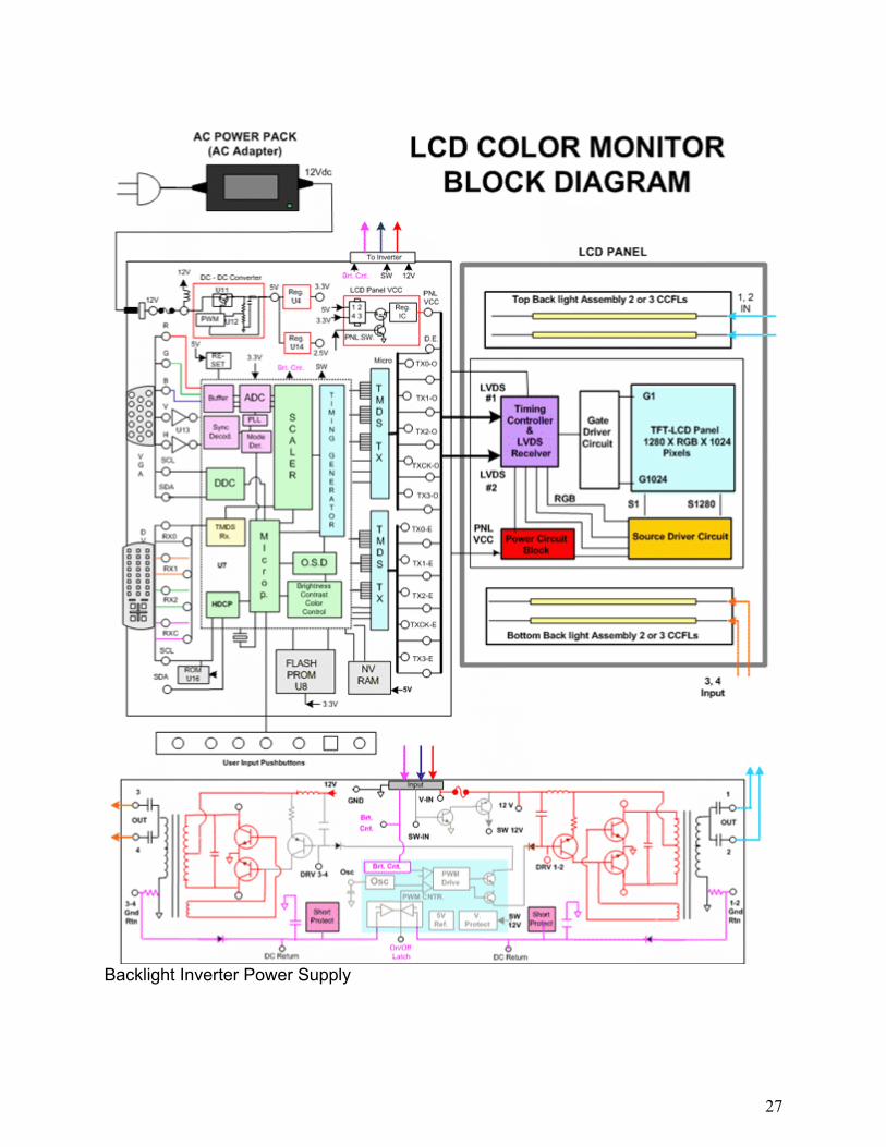
LCD Color Monitor Block Diagram AC Power Adapter or “Power Pack”: Takes 120VAC input voltage from electric outlet and converts to a DC voltage (12V) output to power the LCD color monitor. Main Signal Processing Circuit Board: Contains the low voltage power supplies to power all of the LCD monitors circuits including the main signal processor board, LCD panel and backlight inverter power supply. Contains signal inputs and processing circuits to derive the LVDS output used to interface to the LCD panel. Generates user control menus and accepts inputs from user key board. User Input Pushbutton Panel: Contains the pushbuttons that permit a user to change picture adjustments etc. Backlight Inverter Power Supply: Produces multiple high voltage, high frequency AC sine-wave outputs from a low voltage DC input to power all the backlight bulbs. LCD Display Panel: Produces the picture image by sequentially and repeatedly lighting each pixel element to its proper proportion of red, green and blue light. Accepts an LVDS digital signal representing pixel information and converts to signals to drive the individual pixels in the display panel. CCFL: (Cold Cathode Florescent Lamp) Light bulbs – long skinny florescent tubes that line the top and bottom rear of the LCD display panel. Provide the light that illuminates the face or screen of the LCD panel to illuminate red, green and blue pixels. Suggested Activity: LCD Color Monitor Input/Output Signal Familiarization

29
VGA INPUT – RGBVH The most common signal input used in computer monitors and modern gaming monitors may be called the “VGA Input.” This input connector was initially introduced by IBM during the late 1980s to interface the computer to its computer monitor. The initial signal carried over this connector was the VGA signal resolution format. The connector itself is a 15 pin 3 row connector that is a high density plug. It is often referred to as an HD-15 connector. Since its introduction it has remained the main interface connector for all analog signals between a computer and computer monitor. The signals passed through the HD-15 plug to the input of a computer monitor are analog signals. The signals consist of three separate red, green, and blue signals which make-up the video signal seen on the display. Two additional signals, vertical and horizontal sync, are passed through the cable to synchronize the scanning circuits of the display and/or to indicate the resolution of the input signal. The analog red, green and blue video signals carrier on the HD-15 plug can be any level between 0.0v and .70 volts. The level represents all shades of red, green and blue between no color (0.0V) and full color saturation (.7V). If all 3 colors are considered together, 0.0V is black and .7V is white. In theory, there are an infinite number of color level combinations and shades of grey. In reality, the computer’s video card has a defined number of amplitude output steps which limits the number of color combinations. Analog RGBVH signals Vertical and horizontal sync pulses are output to the computer monitor to synchronize the CRT’s horizontal and vertical scanning circuits. The sync frequencies also indicate to the display’s mode control circuits the resolution format of the incoming signal. To determine the input resolution the display must count the vertical and horizontal sync frequency and note the polarity of the sync pulses.

30
Pin-out of HD-15 Connector The sync signal level at the computer monitor inputs are TTL or 5VPP. The sync signals are short duration pulses either positive or negative in polarity. Commonly RBGHV signals are interfaced through the HD-15 connector using 5 separate signal lines. Pins 1, 2, and 3 contain the red, green, and blue video signals. Pin 13 and 14 contain the separate sync signals.
Schematic diagram of VGA input circuitry on the Sencore LCD Color Trainer
(Courtesy of Kristel) The VGA input signal jack and input circuitry is shown in the schematic. Input signals are input to pins 1, 2, and 3 (red, green, blue). R63, R64, and R65 present a 75 ohm impedance to the input signals. Input signals are buffered with 100 ohm resistors and capacitively coupled to the IC input. Horizontal sync is input to pin 13 and vertical sync is input to pin 14 of the VGA input jack. Zener diodes limit the positive voltage level to approximately 5.6V to protect the IC inputs from excessive voltage. The sync inputs are buffered and inverted by U13A and U13B. The outputs are input to signal processor IC. Suggested Activity: Performance Testing the VGA Input

31
The New Digital Video Interface – DVI The future of interfacing video signals from a source to a display is going digital. The new Digital Visual Interface (DVI) has skyrocketed in popularity with the increasing number of computer flat panel displays, non-CRT data projectors and HDTV displays. Its no longer just for computer flat-panel monitors. This article explains the basics of the new DVI signal and interface connector and shows how to test video displays equipped with a DVI input using the Sencore “VideoPro.” Why Digital - The History In an analog CRT display, a red, green and blue electron beam scans their respective color phosphors on the CRT face. The intensity of the electron beam(s) determines the level of red, green or blue light output. The electron beam intensity is determined by the analog voltage level applied to the control elements of the electron gun. The varying voltage levels during the beam scanning process produces a display image. Repeated scanning produces a new and changing video on the display. A non CRT display (LCD, plasma, DLP) is made-up of rows and columns of cells (picture elements or pixels) each containing a red, green, blue section. Each cell section can be identified and addressed with specific red, green, blue on/off instructions to recreate a displayed image. Periodically and systematically updating each pixel creates a new and changing video on the display. Addressing each pixel with on/off commands and clocking the activity is the work of digital processing circuitry. When CRT computer monitors and TVs dominated the market until the middle 1990s it was accepted that these analog driven displays required an analog input signal. Therefore, computer makers employed computer video cards with digital-to-analog converters which converted the digital data representing the video picture to an analog output video. A RAMDAC (Random Access Memory Digital to Analog Converter) was used. Standard scanning formats VGA, SVGA, VESA, and MAC formats specified the analog signal scanning frequencies, pixels and sync timing. The introduction of LCD flat-panel computer monitors forced industry experts to rethink the connection between a computer and a display. Since an LCD flat panel display uses digital techniques to drive the LCD panel, the conventional analog VGA, VESA, or MAC input signals required an analog-to-digital conversion before they could be displayed. It made sense that a direct digital connection would eliminate signal degradation caused by the D/A and A/D conversions plus a digital signal interface could be less susceptible to noise, crosstalk, and signal losses between the source and display. Initial efforts to define a digital interface began in 1996 but it was not until 1998 that the DDWG (Digital Display Working Group) began to define a standard that would gain broad acceptance. In April of 1999, the resulting DVI specification was published. The specification gained quick acceptance due to its compatibility with early VESA interface connectors and digital formats plus its versatility and scalability.

32
A digital interface signal to a display that digitally produces a display image improves picture quality and eliminates unnecessary circuit complexity and cost.
DVI - Transition Minimized Differential Signaling (TMDS) DVI uses a standard to transmit data to a display developed by Silicon Image, called Transition Minimized Differential Signaling (TMSD). TMDS produces a digital signal optimized to reduce the number of high to low logic transitions on the line. This reduces EMI (Electromagnetic interference) which allows for faster signal transfer rates and decoding accuracy. The differential circuitry in TMDS produces a complementary signal balanced on two wires with a limited amplitude enabling use of twisted pair wires instead of more expensive coaxial cables. TMDS consists of a transmitter that encodes and serially transmits a digital data stream over the twisted pair wires to a TMDS receiver. Video and sync information are serialized and sent over three sets of twisted pair wires, one set for red, green and blue data channels. An additional pair of wires is used to transmit the clock signal needed to decode the signal. TMDS uses an encoding algorithm that converts 8 bits of data representing pixel values into a 10 bit transition minimized, DC balanced character using two stages. The first stage produces the transition minimized nine-bit code word from the input eight bit pixel value. The code word is derived from sequential XOR or XNOR logic functions of a known bit sequence. The ninth bit of the code word identifies which logic function was used so the decoder can reverse the process. The second stage performs an approximate DC balance on the transmitted data stream by selectively inverting the eight data bits of the 9 bit code word. A tenth bit is added to the code word to indicate when the inversion has been made. The encoder determines when to invert the next TMDS character based upon the running disparity between the number of ones and zeros found in the current code word. If too many ones were contained in the previous word and the current word has more ones than zeros, the code work is inverted. The encoder determines the need to invert the word based upon the tenth bit of the TMDS character.

33
The TMDS receiver synchronizes itself to the character sets contained in the data to recover and decode the red, green and blue signal data. The TMDS clock channel carries a character-rate frequency reference. The receiver/decoder produces a bit-rate sample clock based upon this reference which is adjusted in phase for each of the data streams enabling proper decoding.
Block Diagram of a TMDS encoder and decoder used for DVI. The DVI specification calls for at least one TMDS "link" which consists of three data channels (RGB) and one clock control channel. According to the DVI specification, a TMDS link may operate at up to 165MHz. A single 10-bit TMDS link offers 1.65Gbps of bandwidth which is enough for a 1920 x 1080 resolution refreshed at 60Hz on a digital flat panel. The resolution easily handles current HDTV resolution formats. In order to keep the specification as flexible as possible, a second TMDS link may be used. This link must operate at the same frequency as the primary link, meaning that in order to obtain 2Gbps of bandwidth each link must operate at 100MHz (100MHz x 2 x 10-bits). DVI Connectors The DDWG felt that the transition from analog to digital monitor interfacing should be gradual, with capability to support analog VGA/VESA formats for some time. With this in mind they created two connector versions; a DVI-D (digital) version, for digital interfacing only, and a DVI-I (integrated) version, which contains both analog and digital interfaces. 1. DVI – Digital (DVI-D) to support only digital displays. 2. DVI-Integrated (DVI-I) to support digital displays and be backward compatible with analog
displays. The two DVI connector styles provide manufacturers with the flexibility to support digital devices while remaining backwards compatible with analog devices. DVI is also backwards compatible with two earlier digital formats which used TMDS technology through the use of adapters. The Plug and Display (P & D) and Digital Flat Panel (DFP) standards. The digital DVI-D connector may have 24 pins that can accommodate a dual link TMDS connection. If a single link TMDS connection is used only 12 of the 24 pins are needed. Therefore, connectors and cables intended only for single link TMDS may only have 12 of the possible 24 pins in the main body of the connector.

34
DVI specifications define a DVI-D (Digital only) connector and DVI-I (Integrated digital & analog) connector.
The DVI-I receptacle adds additional connection pins to the connector. Connections C1 through C5 provide red, green, blue, and sync signals for an analog connection to a display. Pin 8 of the main body is used for vertical sync. An analog connection is possible with DVI connectors and cables that contain these additional pins. A DVI-I to VGA (15 pin HD) adapter can be used to feed analog signals contained on a DVI connector or cable to the analog inputs of a display with a traditional VGA plug. You should be aware that with two variations of these connectors there is a possibility of interoperability. Using a DVI-D connector/cable will not work to transport analog signals. Also, using a DVI-D connector/cable with only 18 of the possible 24 pins could not be used for dual link DVI. “VideoPro” Integrated DVI Generator & DVI Formats The Sencore “VideoPro” models VP401 or VP403 integrate a DVI digital signal generator with a multi-media analog signal generator. The “VideoPro” outputs all possible analog signal types including composite video (NTSC or PAL) component video (Y,PrPb) and RGB video. The VP401 adds DVI to the basic analog signals and the VP403 adds DVI plus ATSC digital RF signals. DVI is output from the VP401 or VP403 with the standard DVI-I connector. DVI signals are in a single link format and utilize TMDS channels D0, D1 and D2. Generator analog output signal are interfaced through the DVI connector using pins 8, C1 – C5. The “VideoPro” comes equipped with a DVI-to-VGA adapter and VGA to BNC connector cable permitting easy interface to all analog RGB or YPrPb display inputs.
The VideoPro Multi-media generator outputs all analog and
DVI signal outputs through the standard DVI connector.
35
The DVI output signals from the “VideoPro” include many different resolution formats for testing DVI inputs found on many types of video displays and projectors. Computer monitors with DVI capability display formats derived from VESA display standards. Consumer TV and HDTV-compatible video displays are capable of displaying HDTV formats in various resolutions. Some HDTV displays and projectors are capable of displaying both computer monitor formats and HDTV formats.
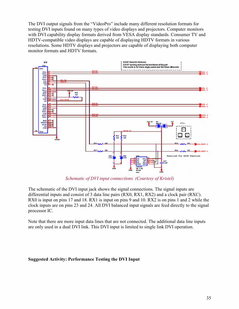
Schematic of DVI input connections. (Courtesy of Kristel) The schematic of the DVI input jack shows the signal connections. The signal inputs are differential inputs and consist of 3 data line pairs (RX0, RX1, RX2) and a clock pair (RXC). RX0 is input on pins 17 and 18. RX1 is input on pins 9 and 10. RX2 is on pins 1 and 2 while the clock inputs are on pins 23 and 24. All DVI balanced input signals are feed directly to the signal processor IC. Note that there are more input data lines that are not connected. The additional data line inputs are only used in a dual DVI link. This DVI input is limited to single link DVI operation. Suggested Activity: Performance Testing the DVI Input

36
Display Data Channel (DDC) Display Data Channel (DDC) is a communications channel between a signal source and a display. DDC was originally developed to enable a computer to learn what resolution formats a display that was connected to its video output was capable of displaying. This was in support of Plug & Play protocols developed through the Video Electronic Standard Association (VESA). Once the computer learned what formats the monitor could display, it automatically selected the highest resolution format for optimum performance. DDC was originally specified for use with standard VGA 15 pin HD connectors. Since its definition, all newer connection plugs, including DVI and EVC, have specified pins for DDC compatibility. DDC is no longer confined to computers and computer monitors as other display devices and signal sources are integrating DDC capabilities.
Many displays talk to the computer through a Display Data Channel in the monitor’s signal cable.
DDC uses an I2C communications bus between the computer or host device. This bus uses two lines including a serial clock (SCL) line and a serial data (SDA) line. Communication over these lines can be either uni-directional or bi-directional. Several revisions of DDC protocols have evolved. DDC1 is uni-directional from the display to the host, display data is sent continuously, clocked by vertical sync. DDC2B, DDC2B+ and DDC2AB are bi-directional, with the host initiating a request for data and the display then transferring the data. DDC2B involves a simple command by the host followed by reading data (EDID information) from the I2C slave memory IC. DDC2B is used by the VideoPro 400 series generators.
Data related to the computer monitor is communicated to the computer. The data is stored in a memory IC (ROM) and clocked to the computer with the 12C data bus (SDA-2) line.

37
Extended Display Identification Data (EDID) defines the data and orientation of the data over the DDC channel. The data can include manufacturing and model information but more importantly resolution information regarding the compatible formats that display can properly display. When the EDID data is decoded, a host device can determine which of the standard VESA formats, along with other formats, are compatible with the display. The VideoPro 400 series reads the EDID data and lists the formats that can be produced by the generator. These formats can be selected and output to the display in the DDC Step sub-menu within the Learn Formats function of the VideoPro. The DVI connector is DDC compatible. DVI connector pin 6 is the DDC clock line and pin 7 is the DDC data line. Pin 8 supplies an analog vertical sync signal. Pin 14 of the DVI connector is available for use by the host to supply 5V to the display’s DDC circuits. The display has the option to use this supply to keep the DDC capable circuits active while powered off. Pin 16 is a detection pin used to sense when a display is plugged into the DVI jack. When the host detects over 2.4V or logic high on pin 16, it can begin a DDC test as part of the plug and play setup. The Sencore VideoPro generator does not employ a host detection feature. DDC is implemented by pressing the Learn Formats pushbutton. Note: See the schematic of the DDC circuits in the Sencore color LCD monitor in the DVI section of this workbook. Suggested Activity: DDC (Display Data Channel Test)

38
Testing the AC Power Adapter or SMPS LCD color displays derive a DC supply voltage from the AC line to power the LCD display. The power supply may be a circuit board mounted in the display with discrete filter, rectifier, and switch mode power supply regulating circuitry. The circuit board would have a 120VAC input and output one or possibly two DC voltages to power the other display circuit boards.
Many new LCD color displays instead of having an additional circuit board have gone to using a separate AC power pack. Technology advances have miniaturized a switch mode power supply so it can fit into a small enclosed power pack. No matter if the main DC power supply is a power adapter or circuit board SMPS, it must deliver a regulated output DC voltage with the needed current/power output to power the LCD Color Display circuits. The circuit current/power demand of the LCD display depends on the size of the screen and the number of CCFL backlight lamps that are used. It is not uncommon for an 18-19 inch LCD display to consume or demand 50-60 watts. If the AC power pack must deliver 50 watts to an LCD color display and its output is a common 12V DC, then it must be capable of outputting slightly over 4 amps of current to adequately power the display. To test an AC power pack you should be sure that it outputs its rated DCV (+/- .5Volts) under the normal operational load of the LCD color monitor. Connect the LCD display and produce a test pattern on the screen. Use a voltmeter to test the DCV input to be sure it is regulated to the proper voltage, such as with a 12V supply (11.5-12.5V). While this seems simple when the display is working it is not so simple when the display or AC power pack is defective. The DC voltage may be near normal when not connected to the display but be pulled very low when connected to the LCD display. The display could be defective drawing to much current loading the AC power pack or the AC power pack may be defective and unable to output the 4A while regulating the output DC voltage properly. To determine if the AC Power Adapter is working properly it should be load tested with the Sencore PSL60. The PSL60 provides an adjustable resistive load and monitors the current/watts in the load and the output voltage from the power pack simultaneously. To test the AC Power Pack, connect the PSL60 as shown. Set the PSL60 Volts/Power Range Switch to the 4-20V 60Watt position. Start with the PLS60 Current Set Control near minimum. Set the PR570 Current/Power Switch to CURRENT. Increase the PSL60 Current Set Control increasing the current draw from the Power Pack through a range of 1 watt to 40 watts. The DC voltage output from the Power Pack as shown on the PSL60 decreases but should remain above 11.5 volts.

39
Note: The test leads to the PSL60 exhibit several tenths of a volt drop with currents 3-5 amps. Therefore, the PSL60 reads lower voltage by .3-.4 volts than is actually output from the power adapter. Suggested Activity: Load Testing the AC Power Adapter – PSL60 Display Power Management Signaling Most new monitors, including LCD monitors support Display Power Management Signaling (DPMS). DPMS allows the computer to progressively signal the monitor into power reducing modes in three stages as the computer is unused for a period of time. The monitor responds to signals from the computer to control the level of shutdown or resumption of normal operation. Many displays use DPMS signaling to tell the monitor that the computer is not being used and it is OK to go to power reducing modes to save energy. DPMS signals the monitor by removing vertical and/or horizontal sync to the display. DPMS represents a standard for implementing video adapter signaling adopted by the Video Electronics Standards Association (VESA). The system allows the computer to signal the monitor through the video adapter card, when the computer has been inactive for some period of time. This allows the monitor’s control circuits to switch the monitor into one of three progressive power saving modes until the computer senses mouse or keyboard activity. The period of inactivity required before the computer initiates each subsequent level of power management is determined by a user-adjustable power management setup.

40
The monitor is signaled into power saving modes by detecting the disappearance of horizontal sync, vertical sync, or both to its signal input. The DPMS standard specifies three savings modes including standby, suspend, and off. DPMS specifies the first level of power reduction, standby, as triggered by a loss of horizontal sync input. The second level of power reduction, suspend, is triggered by a loss of vertical sync input. Finally, off is triggered by the loss of horizontal and vertical sync to the monitor’s signal input. Traditionally in CRT displays the stand-by mode represented only a marginal reduction of power and the ability to very quickly restore an image to the CRT display screen. It is often as simple as blanking the video to the CRT. Standby typically required the circuits continue to heat the filament of the CRT for fast picture recovery. The second level of power reduction, suspend, represented a substantial reduction in power and the ability to resume operation in a moderate amount of time. The third level of power reduction, off, virtually reduces power consumption to only a few watts. Power consumption is typically limited to keeping the control microprocessor active and a significant amount of time is required for picture recovery. DPMS reduction in CRT displays was governed by shutting down power consuming deflection and high voltage circuits. The three levels of power reduction fit well into CRT power reducing steps. However, in LCD displays most of the signal processing circuitry, including the LCD panel are low voltage, low power circuits. An insignificant percentage of power reduction is achieved by shutting power off to these circuits. Power reduction in LCD displays centers around turning off the CCFL lamps. Each lamp of a 4 or 6 lamp display typically consumes 8-10 Watts of power. Shutting off all the backlight inverter supply eliminates the majority of power consumption in the LCD display. While the LCD display detects all 3 power reducing steps defined by DPMS it implements the “off” level of power reduction for all combinations of sync signaling. Loss of either or both sync signals causes the LCD monitor to switch off supply voltage to the LCD panel (VCC PNL) and switch of the Inverter Power Supply. Power consumption is reduced down to only a few watts to power the Power Adapter and microprocessor on the main circuit board. DPMS Mode H. Sync V. Sync Power Savings On On On None Standby Off On Minimal Suspend On Off Substantial Off Off Off Maximum Suggested Activity: Power Management - PR570 Current/Power Familiarization

41
LCD Color Monitor Troubleshooting Main Signal Processor & Control Circuits The main signal processor and controller circuit board contains the low voltage power supplies to power much of the LCD monitor circuitry. The low voltage power supplies on this board power the main signal processor board itself, the LCD panel and backlight inverter power supply.
The main signal processor and controller circuit board accepts signal inputs. There is a standard common VGA input jack and an optional DVI input jack. Signals from the two inputs are selected and processed for output to the LCD panel. The main signal processing IC outputs red, green blue digital signals along with control signals to the LVDS transmitter ICs. The main signal processor/controller circuitry outputs digital LVDS interface signals compatible with the native resolution of the LCD panel. The main signal processor/controller circuit board accepts input commands from the user pushbutton panel. The inputs command the microprocessor to generate the OSD display and permit user input or adjustment of picture and OSD parameters. Following is a brief description of the circuit blocks. Buffer: Presents a 75 ohm impedance to the input signals. Buffers the signal inputs so a short on the input does not cause board damage. ADC: Analog-to-Digital-Converter samples the level of the red, green, blue video inputs and converts to digital values to represent the signal levels.

42
Sync Decoder: Buffers the sync inputs and changes the sync to a common polarity and duty-cycle. Provides sync frequency and polarity information to the microprocessor so it can identify the input signal resolution. This enables proper EEPROM data for picture setup. PLL: (Phase-lock-loop) Generates a sampling clock for the analog digital converter based upon the sync input and the detected format resolution. Mode Detect: Detects the resolution of the input signal based upon the input sync frequency and polarities. Provides input signal resolution information to the microprocessor so the proper EEPROM data can be retrieved and picture control and signal timing parameters are established. Scaler: Performs scaling function so the input signal resolution and corresponding digital samples collected are converted to the correct number of digital values to address the pixels of the LCD panel at its native resolution. Timing Generator: Creates the signal timing used to gate picture or frame values in and out of memory and time the delivery of digital data to the LCD panel with the TMDS transmitter. TMDS TX: Multiplexes the digital data onto 4 data lines and a clock line and produces an LVDS signal interface output. DDC: Display Data Channel: Provides communications data to the signal source, typically a computer video card. The data describes the monitor’s resolution format capabilities. TMDS Rx.: Receives and decodes the multiplexed serial digital data values representing the red, green, blue, sync signals input to the DVI input. Outputs 6 or 8 bit digital values for each color. Microprocessor: Directs operational functions on the signal processor/controller circuit board involving signal processing, scaling, memory read/write, OSD generation, user input commands, DDC etc. OSD: Generates on screen display window and information (values) contained in the window. Interfaces generated video into digital values and times in with each picture frame of panel video. DDC: Display Data Channel provides data to a computer as to the resolution formats the display can properly reproduce. Flash PROM: (Programmable Read Only Memory) Used by the microprocessor. NVRAM: (Non-volatile random access memory) Provides permanent data in memory for microprocessor operation.

43
Block Diagram of the Main Signal Processing/Controller circuit board in an LCD Color Monitor
The main signal processing/controller circuit board is the engine of the LCD color monitor. It performs multiple signal processing operations. The large scale integration IC (IC7) has over 200 pins. It, along with the memory ICs, performs all functional operations. Suggested Activity: Main Signal Processor Board Familiarization

44
Main Signal Processing/Controller Board Power Supplies The main signal processing/controller circuit board typically requires 3 power supply voltages for powering its circuits. It typically requires a 5V, 3.3V, and 2.5V power supply. These voltages are derived from the input 12V from the AC Power Adapter. A DC-to-DC converter is a switching power supply that bucks the voltage down to 5V. The converter output provides a stable or well regulated 5V output. The 5V output feeds linear regulator ICs to drop voltages down to 3.3V and 2.5V outputs. The 3.3V and 2.5V DC supplies are conventional fixed voltage regulators.
Simplified diagram of DC power supplies on main signal processor/controller board. Voltages are input to an LCD panel VCC circuit. A mechanical jumper is used to input a voltage that is appropriate for the LCD panel being used. Some panels operate from 3.3V or 5V while others require 12volt. The jumper enables the processor/controller board to output the appropriate voltage to the LCD panel. In this way the board is compatible with different LCD panels. The DC voltage to the LCD Panel (PNLVCC) is switched on or off with the microprocessor. The microprocessor waits to turn on the panel until there is an OSD message or valid input signal format signal to display. The power stages on the main signal processing/controller board do exhibit component failures causing the board to malfunction. Also, since the power supply circuits feed the LCD panel and inverter power supply it is possible for a main board power supply failure to adversely effect their operation. Troubleshooting the main board power supplies is possible with some knowledge of the circuits and component locations. A schematic of the 5V DC power supply section in the LCD color monitor trainer, courtesy of Kristel, shows the nature of a DC-to-DC switching power supply. It may also be called a “converter” as it converts the 12VDC input to 5 VDC output. The converter is actually a switching mode power supply. U11 (CEM9435A) is comprised of a switching transistor(s) which complete a conduction path from the inputs “S” to its outputs “D.” The IC transistor(s) are pulse width driven at its gate or “G” input on pin 4. The IC serves as a bucking current regulator reducing the voltage down to 5 volts. The chopped output is filtered by L14 and EC20. The pulse width drive is generated and modulated with a PWM IC (U12, AIC1578). Drive is output from pin 6. Feed-back from the supply output is feedback to pin 4 (FB) by divider resistors R34 and R36. The feedback varies the drive PWM to regulate the output. A current sensing resistor, R23, feeds back a DC voltage to U12 (pins 7, 8) relative to the current flowing through it to the output. A shorted load on the 5V output causes the PWM to current limit

45
reducing the output voltage but protecting the power supply from damage. Pin 3 of U12 detects a reduced level of input voltage turning off the PWM drive output.
Schematic of the 5V DC-to-DC
converter power supply (SMPS). Courtesy of Kristel.
The schematic of the power supply used to power the LCD panel (VCC PNL) shows the switched path of DC voltage to power the LCD panel. The 5V, 3.3V, and 12V (not shown) are input to JP1, a connecting plug with 6 connections in which one set of connections is not shown. A mechanical jumper can be removed and placed across the plug to pass the 5V, 3.3V or 12V to the LCD panel (VCC PNL). The DC voltage to the panel is switched with U1. A low or little DC voltage to the “G” input turns the transistor off and does not permit voltage to the output. Little voltage exists at “G” when transistor Q1 is biased on by the microprocessor input to its base. When the microprocessor turns off Q1, the voltage to the G input is pulled up to the input voltage by R1 permitting voltage to pass through U1 to the output. Noise in the DC power supply line to the LCD panel may exist and worsen as the digital clocks increase. Under such conditions, the conventional way of reducing noise, such as a bypass capacitor, is not useful for eliminating high frequency noise. FL 1 (KHLC-010), inserted in the DC power supply line of the electronic circuit board, eliminates octave or high frequency switching noises. (Note: Although shown on schematic it is not installed on circuit board)
Schematic of the power supply on the main signal processor/controller circuit board used to power the
LCD panel (VCC PNL). (Courtesy of Kristel)

46
The schematics of the 3.3V and 2.5V power supply linear regulators.
The 3.3V and 2.5V power supplies operate the digital ICs on the signal processor/controller circuit board. These supply voltages are derived from the 5V power supply. U14 is a surface mount linear regulator IC that outputs a regulated 2.5V. It is an IC package TO-252 and a suitable replacement is a PJ1117CP-2.5. U4 is also a linear regulator but physically larger. A suitable replacement is PJ1084CM.
Suggested Activity: Load Testing 5V Converter Power Supply – PSL60

47
Understanding the LVDS Signal Interface Most LCD color monitors employ an LVDS signal interconnect or interface between the main signal processing/control circuit board and the LCD display panel. LVDS is a system which multiplexes up to 8 bits of color data into a single LVDS differential pair. In all, 8 TTL lines for each color (24 lines) can be serialized into 4 data pairs and a clock pair. At higher resolutions pixels are broken up into odd and even pixels requiring 8 data pairs and 2 clock pairs. Block Diagram LVDS interface LVDS is an industry standard that defines a high-speed, low-power, data-signaling connection. LVDS is used in digital camera interfaces and LCD display interfaces. LVDS is defined by ANSI/TIA/EIA-644 (EIA-644), which specifies electrical characteristics of the driver output and receiver input. Guidelines for bus configuration, cables, and termination are given, but protocols, connectors, and bus structures are not defined in the standards. LVDS overcomes some of the limitations of more traditional digital signal bus standards/ LVDS cuts down on noise and boosts data rates by using extremely low voltage levels (350 mV compares to 2.4 V), which translates to low radiation and less power consumption. LVDS employs differential signaling to filter out noise. The equivalent circuit structure of LVDS includes the transmit differential driver. (See illustration) The output driver has a current source to limit the output to about 3 mA. The output current is steered through the termination resistor. The differential driver produces equal and opposite currents flowing in the transmission lines. The current returns within the wire pair, so the current loop area is small, and therefore generates a low amount of EMI. (electro-magnetic interference) The current source limits any spike current that could occur during transitions. Because there are no spike currents, data rates as high as 1. 5 Gb/s are possible without a substantial increase in power dissipation. In addition, the constant current driver output can tolerate transmission lines shorted together, or to Ground, without creating thermal problems. The differential receiver is a high impedance device that detects differential signals as low as 20 mV and then amplifies them into standard logic levels. The signal has a typical driver offset of 1.2 V, and the receiver accepts an input range of Ground to 2. 4 V. This allows rejection of common-mode noise picked up along the interconnect of up to +/- 1 V.
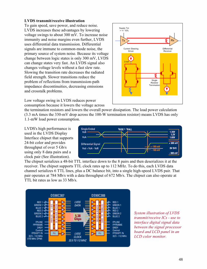
48
LVDS transmit/receive illustration To gain speed, save power, and reduce noise. LVDS increases these advantages by lowering voltage swings to about 300 mV. To increase noise immunity and noise margins even further, LVDS uses differential data transmission. Differential signals are immune to common-mode noise, the primary source of system noise. Because its voltage change between logic states is only 300 mV, LVDS can change states very fast. An LVDS signal also changes voltage levels without a fast slew rate. Slowing the transition rate decreases the radiated field strength. Slower transitions reduce the problem of reflections from transmission-path impedance discontinuities, decreasing emissions and crosstalk problems. Low voltage swing in LVDS reduces power consumption because it lowers the voltage across the termination resistors and lowers the overall power dissipation. The load power calculation (3.3 mA times the 330-mV drop across the 100-W termination resistor) means LVDS has only 1.1-mW load power consumption. LVDS's high performance is used in the LVDS Display Interface chipset that supports 24-bit color and provides throughput of over 5 Gb/s using only 8 data pairs and a clock pair (See illustration). The chipset serializes a 48-bit TTL interface down to the 8 pairs and then deserializes it at the receiver. The chipset supports TTL clock rates up to 112 MHz. To do this, each LVDS data channel serializes 6 TTL lines, plus a DC balance bit, into a single high-speed LVDS pair. That pair operates at 784 Mb/s with a data throughput of 672 Mb/s. The chipset can also operate at TTL bit rates as low as 33 Mb/s.
System illustration of LVDS transmit/receive ICs - use to interface digital signal data between the signal processor board and LCD panel in an LCD color monitor.

49
The block diagram of a transmit and receive IC combination for LVDS shows the inputs and outputs to the transmit and receive ICs. The transmit IC gets 8 data bit line inputs per color to represent the picture information pixel by pixel. The input also has vertical sync, horizontal sync, DE (data enable) and control (CNTL) inputs.
A typical LVDS transmitter IC block diagram. (Note error CLKOUT on Transmitter IC is actually CLKIN) to lock PLL to incoming data rate or dot clock)
The LVDS transmitter IC used in the Sencore LCD Color Monitor trainer has 8 data line inputs, H sync, Vsync, device enable (DE), control, and clock inputs. The DTC34LM85A transmitter IC converts 28 bits of CMOS/TTL data into four LVDS data streams. A CLKIN signal is phased-locked and transmitted in parallel with the data streams over a 5th LVDS link. 24 bits of graphic data, and 3 bits of timing and 1 control data are transmitted at a rate of 595 Mbps per data channel at a transmit clock frequency of 85 MHz. The R_FB pin selects either rising or falling edge trigger of CLKIN. The transmit IC is compatible with DTC34LF/R86 receiver.
Signal processor/controller circuit board. (Courtesy Ceronix)
LVDS Transmitter ICs – Dual channel requires 2 ICs,(dual CH.) in 1280 x 1024 resolution

50
The LVDS transmit ICs are always easy to find on the main signal processor board. Look for the multi-wire interconnect plug between the main signal processor/control circuit board and the LCD panel. National and Doestek both manufacturer LVDS ICs that are illustrated in this workbook and used in LCD color displays. There are as many as 28 inputs to each of the LVDS transmit ICs. These inputs are serialized or multiplexed onto 4 wires for output by LVDS. The clock input and output are considered separately. The inputs and their waveforms are shown in this illustration when using a 16 step grayscale pattern. Note that there are 8 inputs for each color. This is basically a parallel input for each individual data bit of an 8 bit word. In digital video the values range from 00000000 (black), 00000001 (min. red) to 11111111 (digital value 255 – max. red). There are 8 inputs for each color. These inputs are time multiplexed into the LVDS data stream. MSB LSB
R7, R6, R5, R4, R3, R2, R1, R0 Bit ID = Red 0-7 “R” Digital Value 8 Bits
The 8 bit digital color value is identified from LSB (R0) to MSB (R7).
Color Data Reference Input Color Data Red Green Blue
Color MSB LSB MSB LSB MSB LSB
R7 R6 R5 R4 R3 R2 R1 R0 G7 G6 G5 G4 G3 G2 G1 G0 B7 B6 B5 B4 B3 B2 B1 B0
Black 0 0 0 0 0 0 0 0 0 0 0 0 0 0 0 0 0 0 0 0 0 0 0 0
Red (255) 1 1 1 1 1 1 1 1 0 0 0 0 0 0 0 0 0 0 0 0 0 0 0 0
Green (255) 0 0 0 0 0 0 0 0 1 1 1 1 1 1 1 1 0 0 0 0 0 0 0 0
Blue (255) 0 0 0 0 0 0 0 0 0 0 0 0 0 0 0 0 1 1 1 1 1 1 1 1
Cyan 0 0 0 0 0 0 0 0 1 1 1 1 1 1 1 1 1 1 1 1 1 1 1 1
Magenta 1 1 1 1 1 1 1 1 0 0 0 0 0 0 0 0 1 1 1 1 1 1 1 1
Yellow 1 1 1 1 1 1 1 1 1 1 1 1 1 1 1 1 0 0 0 0 0 0 0 0
B A S I C
C O L O R White 1 1 1 1 1 1 1 1 1 1 1 1 1 1 1 1 1 1 1 1 1 1 1 1
Red (000) Dark 0 0 0 0 0 0 0 0 0 0 0 0 0 0 0 0 0 0 0 0 0 0 0 0
Red (001) 0 0 0 0 0 0 0 1 0 0 0 0 0 0 0 0 0 0 0 0 0 0 0 0
Red (002) 0 0 0 0 0 0 1 0 0 0 0 0 0 0 0 0 0 0 0 0 0 0 0 0
-------------- - - - - - - - - - - - - - - - - - - - - - - - -
-------------- - - - - - - - - - - - - - - - - - - - - - - - -
Red (253) 1 1 1 1 1 1 0 1 0 0 0 0 0 0 0 0 0 0 0 0 0 0 0 0
Red (254) 1 1 1 1 1 1 1 0 0 0 0 0 0 0 0 0 0 0 0 0 0 0 0 0
R E D
Red (255) Bright 1 1 1 1 1 1 1 1 0 0 0 0 0 0 0 0 0 0 0 0 0 0 0 0
The table illustrates the 8 bit digital values for the different pixel colors in an LCD display.

51
Note in the red section how the amount of color in a sub-pixel can be assigned values ranging from 0 to 255. R0 to R7 bit values, low 0 or high 1, are input to the LVDS transmitter. Likewise values for the green sub-pixel (G0-G7) and blue sub-pixel (B0-B7) are input to the LVDS transmitter. Each color pixel has 3 x 8 or 24 bits. The 8 bit color inputs for red, green and blue are typically CMOS or TTL level inputs to the LVDS transmit IC. Producing an input waveform to each of the 8 color inputs of the LVDS transmit IC depends on making each pixel make a logic change. The best potential pattern for this is the RASTER pattern of the Sencore VP401 generator. When testing the inputs to the LVDS transmitter with an oscilloscope, put one probe on the clock input and lock into the waveform. Use the other channel input to probe the color inputs and look for a toggle in the input level to confirm the input is working. You may need to include 10-20 cycles of the clock or more before the input toggles on some lines. Look for normal waveforms on the sync, DE and control inputs. Again you should see digital logic voltage changes if the input is working correctly. The figure below illustrates how waveforms appear on some of the color inputs and not others. It is important that when testing inputs you have each of the colors increment in level so that each bit has to change values from high to low.
Input Digital Waveforms to LVDS Transmit IC – 16 Step Grayscale Test Pattern.
The color data inputs, sync, data enable and control inputs are mapped into the different LVDS outputs using assignments as shown. These inputs are mapped into TX values 0 through 27. The maps work for both 6 bit and 8 bit color values.

52
The TX values are mapped into the LVDS channels 0 through 3 as shown in the next figure. Notice how each LVDS channel has most of the bits of a single color but not all. Note how the sync and enable bits are added into the data stream.
Bit map assignment LVDS for 8 bit color, sync, data enable and RSVD input signals.

53
Illustration showing how the color bits, sync, DE, and time multiplexed into four
LVDS data streams.
With a total of 28 different inputs and eventually 4 differential output lines it becomes apparent that somehow that you must squeeze 7 data bits into every output each clock cycle. This requires that a PLL be locked to the incoming clock and that it run faster than the incoming dot clock. You can see from the illustration that the output LVDS data bits have 7 bits for every clock cycle.
Seven data bits are time multiplexed into a data stream during 1 clock cycle.

54
A common 30 pin plug is used to interface LVDS signals to an LCD panel. The table below specifies the pin numbers of this connector and the signal assignments. It is not uncommon to use pin 3 and 4 for data enable (DE) signals.

55
Schematic diagram of LVDS transmitter ICs in Sencore LCD Color Monitor Trainer. (Courtesy of Kristel)
Two LVDS transmit ICs are used when the display resolution becomes larger. This is because the native resolution of the display 1024 x 1280 and 8 bit color requires a large volume of data values. To accomplish this, the display pixels are divided into even and odd pixels. One LVDS processes the even pixels and the other the odd pixels. Using two ICs enables twice as much digital data to be transmitted to the display panel to support displays with higher resolution. Each LVDS transmit IC has 8 inputs for every color, digital vertical sync, digital horizontal sync, digital data enable and clock inputs. Suggested Activity: Main Signal Processor Board Familiarization

56
The LCD Panel The LCD panel is the display module for the LCD color display. It contains a circuit board with electronic circuits. The circuits contain LVDS decoders, DC power supplies, and output timing circuits. Addition driver circuit boards line the top and side edge of the display to connect and apply signal voltages to the row and column connections to individual pixels. CCFL Assemblies: Provides light source at rear of panel typically at the top and bottom. LVDS Receiver: Receives the LVDS signal from the signal processor/controller circuit board. Decodes and outputs the red, green, blue, sync and control digital signals needed by the timing control. Power Circuits: Develops the multiple DC voltages required by the circuits of the LCD panel from a single input voltage to the panel. Timing Controller: Outputs digital data, clock, and timing waveforms to the drivers to coordinate writing of values to the individual pixels of the display to Gate Driver: Applies voltages to gate on the thin film transistors in each sub-pixel of the display. Source Driver: Applies voltages to the source of the sub pixel transistors to determine the intensity of the pixel. LCD Panel: Contains the grid of LCD cells or red, green, blue sub- pixel elements and their drive transistors and electrode connections. Active matrix drive systems are used for LCD monitors and LCD-TV where moving picture applications are required and high picture quality and a fast response are needed. AM-LCDs (active matrix LCD) have no inherent limitation in the number of scan lines, and they present fewer cross-talk issues compared to passive systems. There are many kinds of AMLCD. For their integrated switching devices most use transistors made of deposited thin films, which are therefore called thin-film transistors (TFTs). In AMLCDs a switching device and a storage
capacitor are integrated at the each cross point of the electrodes. Note: The most common semiconducting layer is made of amorphous silicon (a-Si) which is amenable to large-area fabrication using glass substrates. Each sub-pixel has a transistor with electrical connections to its gate and source.

57
In active matrix LCDs, switching transistors (TFTs) or diodes are attached to each pixel to switch each one on or off. X and Y electrodes are formed on the same substrate as TFT (or diode) arrays. The switching signals are applied to the X electrodes. Video signals are then applied to the Y electrodes.
The array of sub-pixels in an LCD panel and electrical connections.
There are 1024 rows and 1280 columns in an SXGA LCD panel resolution.
The process of writing digital values or voltages to each sub-pixel is accomplished in rows. Unlike CRT scanning which moves across the row slowly, all the pixels in a row can be written to simultaneously. Simply the row connection to all the gates is increased to + 15V to 20V turning on all the transistors in that row. Simultaneously the voltages are applied to the columns with voltages to each source. The storage capacitance at the transistor drain to the displays common electrode charges placing a voltage potential across the LCD cell. The voltage causes a varying output level of red, green or blue light from the sub-pixel. The capacitance holds the charge until the cell is written to on the next sequence.
Illustration of how individual sub-pixels are addressed and voltages
applied.

58
By timing the activation of the gate bus-lines (rows) sequentially, and by applying signal voltages to all source bus-lines in sequence with gate switching, each sub-pixel in the panel is addressed and written with a voltage value. This completes a picture frame. The process is repeated every 15-20 mS to update to the next picture frame. Virtually all AMLCDs are designed to produce varying levels - between the most saturated color and the least amount of color a sub-pixel can generate. There can be a discrete numbers of digital levels (256) which are interpreted into voltage levels applied to the source of each sub-pixels or cells. The digital LCD driver ICs (LDI) produce discrete voltage amplitudes, which permits a discrete numbers of shades to be displayed determined by the number of data bits produced by the digital driver. Although there are a total of 256 levels possible in an 8 bit color system, the signal processor can purposefully change the dynamic range of digital values or the end values to perform user adjustments. For example, decreasing the red color level in the user color temperature menu screen reduces the maximum digital level from 255 (max possible in digital system) down to perhaps 245 lowering the source voltage to the red pixels during for a white raster.
Block diagram of LCD panel showing connections to the transistor gate and
source of the LCD sub-pixels. The construction of the LCD panel requires that electrical connections be made to gate and source electrode connections. These connections are at the top and side of the LCD panel. These connections are far too many and tiny to be made with traditional wire and soldering techniques. Instead a TAB (Tape Automated Bonding) process is used to make electrical connections with a TCP (Tape Carrier Package). A TCP is a small flexible tape material with many tiny electrical conductors. It must be precision positioned, heated and pressured into a bond completing the electrical connections. Specialized and expensive equipment is required for this process (Pulse-heated anisotropic- conductive film (ACF) equipment)
Driving an a-Si TFT LCD requires a driving circuit unit consisting of a set of LCD driving IC (LDI) chips and printed-circuit-boards (PCBs). The drive circuit unit can be placed on the backside of the LCD module by using bent Tape Carrier Packages (TCPs)

59
The rear of the LCD panel reveals connections and circuit boards required for display operation. When a metal cover is removed, a circuit board containing electronic circuits is revealed. Feeding this circuit is the LVDS signals from the main signal processor board typically through a wiring harness and 30 pin connector. The wiring harness contains 10 twisted wire pairs for data and clock signals for even and odd pixels. In addition, wires for ground, panel power, and data enable (DE) – optional, are included.
The circuit board mounted on the rear of the panel contains several DC power supplies circuits which take the panel DC input voltage and derive several DC voltages required by the circuit board and panel to operate. A balanced + and – 15V supply, 5V, and 3.3V supplies are typically needed by the LCD panel. A miniature surface mount fuse is located on the DC panel input to the circuit board.
Rear of Philips LM181 LCD panel. The circuit board also contains an integrated LVDS receiver/timing generator IC which recovers LVDS input data and derive the outputs needed by the column and row drivers to read voltages to the display pixels. A circuit board at the top edge contains driver IC used to drive the individual columns (source leads) and edge circuit board contains the driver ICs to drive the rows (gate leads) of the individual pixel transistors. Although it can be disconnected and remove on most LCD panel, the circuit board is considered an integrated part of the LCD panel making replacement and/or repair difficult.
Photo of the Plexiglas plate (right) and film layers in a disassembled LCD panel.
To the rear of the LCD panel is a thick plexiglas plate (Upper right of photo). It provides dispersion of the light emitted from the CCFL lamps at the edges of the panel evenly across the back of the display. The sheets of material between the plexiglas and panel matrix serves to even further disperse the light and reflect it forward through the panel. A polarizer layer passes the light into the LCD panel at the proper polarity.

60
LCD Panel Protection ELECTROSTATIC DISCHARGE CONTROL Since a module is composed of electronic circuits, it is susceptible to electrostatic discharge. Make certain that service persons are connected to ground through wrist band etc. Don’t touch the interface pins directly. PRECAUTIONS FOR STRONG LIGHT EXPOSURE Strong light exposure causes degradation of the polarizer and color filter. STORAGE When storing modules as spares for a long time, the following precautions are necessary. 1. Store them in a dark place. Do not expose the module to sunlight or fluorescent light.
Keep the temperature between 5°C and 35°C at normal humidity. 2. The polarizer surface should not come in contact with any other object. 3. It is recommended that they be stored in the container in which they were shipped. HANDLING PRECAUTIONS FOR PROTECTION FILM The protection film is attached to the bezel with a small masking tape. When the protection film is peeled off, static electricity is generated between the film and polarizer. 1. This should be peeled off slowly and carefully by people who are electrically grounded
and using anti-static ionizing equipment. MOUNTING PRECAUTIONS 1. You must mount a module using holes arranged in the four corners. 2. You should consider the mounting structure so that uneven force (ex. twisted stress) is
not applied to the module. The case on which a module is mounted should have sufficient strength so that external force is not transmitted directly to the module.
3. Please attach the surface transparent protective plate to the surface to protect the polarizer. The transparent protective plate should have sufficient strength to resist external force.
4. Acetic acid type and chlorine type materials for the cover case are not desirable because the former generates corrosive gas by attacking the polarizer at high temperature and the latter causes circuit corrosion by electro-chemical reaction.
5. Do not touch, push or rub the exposed polarizers with glass, tweezers or anything harder than HB pencil lead. And please do not rub with dust clothes with chemical treatment. Do not touch the surface of polarizer with bare hands or greasy cloth. (Some cosmetics are detrimental to the polarizer.)
6. When the surface becomes dusty, please wipe gently with absorbent cotton or other soft materials like chamois soaked with petroleum benzene. Normal-hexane is recommended for cleaning the adhesives used to attach front / rear polarizers. Do not use acetone, toluene and alcohol because they cause chemical damage to the polarizer.
7. Wipe off moisture as soon as possible. Moisture contact with polarizer causes deformations and color fading.
8. Do not open the case because the case provides mechanical structural support for the inside circuits.
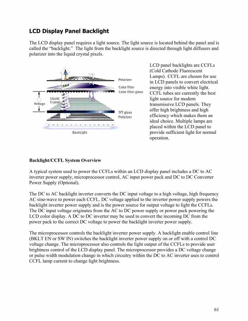
61
LCD Display Panel Backlight The LCD display panel requires a light source. The light source is located behind the panel and is called the “backlight.” The light from the backlight source is directed through light diffusers and polarizer into the liquid crystal pixels.
LCD panel backlights are CCFLs (Cold Cathode Fluorescent Lamps). CCFL are chosen for use in LCD panels to convert electrical energy into visible white light. CCFL tubes are currently the best light source for modern transmissive LCD panels. They offer high brightness and high efficiency which makes them an ideal choice. Multiple lamps are placed within the LCD panel to provide sufficient light for normal operation.
Backlight/CCFL System Overview A typical system used to power the CCFLs within an LCD display panel includes a DC to AC inverter power supply, microprocessor control, AC input power pack and DC to DC Converter Power Supply (Optional). The DC to AC backlight inverter converts the DC input voltage to a high voltage, high frequency AC sine-wave to power each CCFL. DC voltage applied to the inverter power supply powers the backlight inverter power supply and is the power source for output voltage to light the CCFLs. The DC input voltage originates from the AC to DC power supply or power pack powering the LCD color display. A DC to DC inverter may be used to convert the incoming DC from the power pack to the correct DC voltage to power the backlight inverter power supply. The microprocessor controls the backlight inverter power supply. A backlight enable control line (BKLT EN or SW IN) switches the backlight inverter power supply on or off with a control DC voltage change. The microprocessor also controls the light output of the CCFLs to provide user brightness control of the LCD display panel. The microprocessor provides a DC voltage change or pulse width modulation change in which circuitry within the DC to AC inverter uses to control CCFL lamp current to change light brightness.

62
Example of connection diagram from the main signal processing board
to an inverter power supply in a Ceronix LCD monitor. Cold Cathode Fluorescent Lamps (CCFL) CCFL lamps are more efficient in comparison to other light sources. CCFL bulbs convert about 20% of the applied energy into light in the 380-780 nm range. Lamp diameter and length vary which affect their operating parameters.
The cold cathode electrodes of the lamp are comprised of a nickel plated iron structure, containing pockets of mercury during lamp manufacturing. The cathode structure retains the mercury until released by heating the structure using RF energy after the lamp envelope is sealed. The typical CCFL contains from 2-10 mg of mercury. The cathode structure contains a gettering material on its surface to remove damaging residual gases. The getter material is comprised of an allowance of 84% ZR and 16% Al. With a lamp operated from alternating current the cold cathodes alternate polarity. The phosphor coating on the inside of the glass envelope is a tri-phosphor RGB type. It is composed of red, green, and blue emitting phosphors. Varying the phosphor ratios change the white light emitted. Summary:
1. Cold cathode electrodes – nickel plated iron – initially contains pockets of mercury. 2. Mercury dispensed into lamp after it is sealed using RF energy – 2-10 mg mercury in
typical CCFL. 3. A getter element works to remove unwanted gases from the sealed enclosure. The getter
is comprised of 84% Zr and 16% AL. 4. Tri-phosphor coating on the inside of the glass enclosure contains red, green and, blue
emitting phosphors 5. The sealed envelope contains mercury and fill gas (argon) with a pressure of 2-6 Torr.
(Low Pressure)

63
Electric Energy or voltage is introduced into the lamp via the cold cathode electrodes on each end of the lamp. The applied voltage accelerates electrons between the 2 electrodes. The applied electrical voltage is actually a high voltage AC so the electrodes alternate being cathode & anode and the current alternates. Electrons traveling between elements collide with mercury atoms releasing ultraviolet energy. The ultraviolet discharge or ionization of the mercury stimulates the phosphor increasing the 253.7 nm wavelength (ultraviolet) energy to visible light frequencies (red, green, blue). Equal energy red, green and blue results in white light emitted from the lamp.
Ionization is enhanced by adding a fill gas (argon). Adding argon enhances ionization and lowers the required voltage. The fill gas (argon) excites the argon atoms releasing an electron which may also collide with a mercury atom enhancing ionization. Ultraviolet energy strikes the phosphors resulting in white light
CCFLs have a limited lifespan. Ion bombardment of the phosphor over time causes the inner surface of the phosphor to become non-luminescent. Ion bombardment of the phosphor over time causes some phosphors to absorb the mercury causing brightness deterioration.
A typical CCFL life rating specification is approximately 20,000 hours before its brightness is 50% of the lamps initial output at a drive current of 5 mArms. This equates to approximately 2.28 years if the display is operated 24 hours a day. Improvements have increased the usable life of CCFLs in LCD panels. The Philips LM181E06 LCD Panel has a lamp life time specification of 40,000 hours before lamp brightness is reduced to 50% of its initial value. Backlight Inverter Power Supply The CCFLs are energized with applied voltage to its test leads. Typical voltages required by CCFL bulbs are an AC voltage. The most ideal voltage is a pure sine-wave. Sine-wave voltages range from 200-1000 VRMS and frequencies range from 20-100 kHz. CCFLs cannot be operated with DC voltage. DC operation causes decrease light output as the mercury migrates to the cathode element. Gradually a pink glow results from argon gas at the anode end.

64
A CCFL tube needs high voltage to begin ionization. The starting or striking voltage generally requires over 1,000 VRMS. Once ionization is started the voltage can be reduced for more efficient operation. The running or operating voltage is generally between 200 and 1000 volts rms. The starting and operating voltages increase as the size of the CCFL increase. The “Inverter” power supply supplies the voltage required by a CCFL tube to operate and produce light. The inverter changes the low level DC voltage input to a high voltage, high frequency AC voltage to each CCFL tube. The inverter starts bulb ionization and maintains ionization at a reduced AC voltage for efficient light production. A typical inverter is a DC to AC converter power supply. It receives approximately 9 to 13VDC to its input and outputs the required AC voltage to run a particular CCFL bulb. Inverter design parameters are tailored to match the operating characteristics of a particular CCFL bulb known to be within an LCD panel. Furthermore, it would have the appropriate number of outputs for each CCFL within an LCD panel. Suggested Activity: Backlight Inverter Power Supply Familiarization

65
LCD Color Monitor Troubleshooting The first objective to isolating a defect in an LCD color display is to determine which circuit board or module is defective. Once this is determined, a decision can be made to replace the circuit board or attempt to isolate the defect to a component that can be replaced. This section concentrates on a process to isolate the defect to the 1) AC Power Adapter, 2) Main signal Processor/Controller Board, 3) Backlight Inverter Power Supply 4) CCFL Bulb or 5) LCD panel. The first step in troubleshooting an LCD display is to apply power to the display with the PR570 and input the proper test signal from a generator to the monitor’s input and note the display symptoms. Useful information regarding the LCD color monitor symptoms can be obtained by looking at the PR570 Current/Power meter, LCD display indicator light and LCD picture on its screen. PR570 Current/Power Indications: The current indicator provides useful information regarding the operation of the LCD color monitor. Normal current/power indicates the monitor’s power supplies and backlight inverter power supply are working and that the CCFL bulbs are lit and working. Substantial reduction in current (<.1 amp) or power (<15W) indicates a problem with the inverter power supply or CCFL bulbs. Note: Each bulb typically draws 6-8 watts so when the backlight inverter supply is not working the power consumption decreases (7 watts X 6 bulbs = 42 watts). This decrease is very evident on the PR570 from the normal 50-60W when working normally. Picture Symptoms: The most common picture symptom in an LCD color monitor is a complete loss of picture or dark display. This occurs with problems in the LCD panel, backlight inverter power supply, or main signal processor/controller circuit board. Occasionally poor picture symptoms will be displayed, such as a loss of a color or lines in the display. When this occurs you should check the second DVI input to see if the same symptom results. If symptoms improve, the problem is likely related to the other input or the signal processing circuitry. Indicator Light: LCD color displays have an indicator light on the user push-button panel. The light indicates the presence and recognition from the display when a good usable signal is input to the display. An illuminated light indicates power supply circuits to the LCD display are likely OK. An orange light indicates the input signal is not a format the display can scale for display or that the input sync signals are low or missing. A green light indicates the input signal is a recognizable format and that the signal processing circuits are working to display the signal. OSD Menu Display: The presence of an OSD display window on the LCD screen is an important indicator when troubleshooting. When a normal OSD screen is observed, the power supplies to the LCD panel and within the microprocessor/control IC are working. Also the LCD panel is working and the inverter power supply is working and powering the CCFLs. A missing OSD screen can result from a defect in any area of the LCD color display.

66
Suggested Activity: Main Hands-On Troubleshooting Activity

67
Backlight Inverter Power Supply Theory The backlight inverter power supply consists of a tuned circuit or oscillator that generates an AC voltage. A voltage input ranging from 8-14V powers the oscillator. Part of the oscillator is a transformer with a secondary winding to output the AC voltage to the CCFL bulb(s). The output is also tuned with a capacitor forming a resonant circuit with the CCFL in series with the capacitor.
A control circuit consisting of an IC is interfaced to the oscillator typically through a driver transistor. The control circuit has the ability to turn the oscillator on and off. This provides on/off control and the ability to control the output for user brightness control of the CCFL lamps. The inverter power supply has a DC power supply input to power the inverter. An additional voltage input is used to switch voltage to the control IC to turn the inverter power supply on and off. A third input is a brightness control input from the microprocessor on the main signal processor/ control circuit board. Multiple Backlight Inverter Outputs Backlight inverter power supplies are designed to be used to drive different LCD panels. Typically the inverter power supply is designed to be used with certain LCD panels with known CCFL bulb characteristics.
Backlight inverter power supplies have multiple outputs and are designed for particular LCD panels.
LCD panels have multiple bulbs. Popular computer monitor LCD panels ranging 18-19 inch have 4 or 6 CCFL bulbs. Larger LCD panels may have more CCFL bulbs. The inverter power supply must be designed to output to each of the CCFL bulbs in a particular LCD panel.

68
Simplified schematic of LCD Computer Monitor Trainer showing two oscillator sections (red) controlled by common IC controller.
The simplified schematic of the backlight inverter power supply used in the Sencore LCD monitor trainer uses two identical royer oscillators (red). The oscillators are switched on/off and controlled by a common controller IC (blue). The controller IC has two outputs to drive 1-2 and drive 3-4 transistor which turn on/off the oscillators (red). The inverter power supply is switched on by a voltage applied to the SW-IN input to the supply. The voltage biases on a dual transistor switch passing voltage to the voltage input to the IC (SW-12V) Once powered on the IC begins to develop drive with an internal IC oscillator and external RC time constant. The sawtooth waveform may be measured at the OSC test point. The IC oscillator is used to output to the drive transistors for brightness control PWM. An op-amp comparator in the IC provides shutdown protection by disabling its drive output in the event of excessive output voltage, open load protection, or short circuit protection. Transformer secondaries contain multiple series capacitors to feed multiple CCFL bulbs. Two outputs are shown by the diagram but 3 outputs are used to feed the Philips LM181 panel used by the Sencore LCD computer monitor trainer. Backlight Inverter Oscillator Backlight inverter power supplies are DC to AC inverters designed to produce a specific voltage, frequency and output current to a specific CCFL tube. The inverter supply is typically matched to the LCD panel containing the know type of CCFL tubes. The typical backlight inverter supply uses a classic current-fed two transistor inverter circuit. The circuit is based upon a royer oscillator which has a tuned resonant primary circuit. The transformer secondary along with a capacitor and CCFL bulb form a secondary resonant circuit. These tuned circuits produce a sine-wave output although the CCFL current waveform is not a perfect sine-way. Inverters with this design are 80-90% efficient. The royer oscillator primary contains two amplifier transistors to sustain oscillation produced by the transformer primary and primary capacitor. A center tap DC current input powers the oscillator. Each end of the transformer primary contains feedback to the base of one of the transistors. The transistors alternately conduct via the feedback from the out-of-phase transformer primary ends. Inductance and capacitance values produce a frequency of 20-100 kHz.

69
A common backlight inverter power supply circuit has a royer oscillator primary and tuned secondary. The secondary circuit consists of a tuned circuit including the transformer secondary winding, series capacitor and high impedance CCFL lamp. The impedance of the lamp is very high. The impedance when lit ranges from 50k -200 k ohm depending on the lamp size and diameter. The impedance of the unlit lamp is infinite or open.
The secondary series capacitor ranges from 12pfd to 39 pfd. The capacitor becomes a high impedance in series with the output. The secondary capacitor plays a key role in starting the CCFL lamps. The capacitor acts as a ballast, providing high impedance output during startup which applies a higher than normal output voltage across the CCFL lamp. Once the lamps are on the capacitor impedance is responsible for a constant current output to the CCFL lamps. The circuit produces its nominal output current into any load condition including a short circuit.
The CCFL equivalent circuit when lit is resistive in the range of 50 – 200 K ohms.
Suggested Activity: Backlight Inverter Power Supply Familiarization

70
Controlling CCFL Brightness CCFL current is the prime determinate in converting electrical power into brightness. The current flowing in the CCFL bulb is primary determined by the design of the inverter, mainly the voltage input to the royer oscillator, output series capacitor value, and circuit efficiency. Circuit efficiency is high nearing 90%. Brightness control of the LCD display involves varying the current in the CCFL bulbs. There are two basic methods for dimming the CCFL tubes. The first is an analog approach which simply reduces the current through the tubes by reducing voltage to the inverter. The second is more of a digital method in which the inverter output is turned on and off at a chopped frequency that is not visible effectively reducing or increasing the output current. This pulse width modulation method is the preferred method as it provides a wider dimming range.
Analog dimming changes the output amplitude and CCFL current.
PWM (Pulse Width Modulation) interrupts the output at a rate that is not visible effectively changing the output current and CCFL brightness.
Analog Dimming: Analog dimming can be implemented by using a buck converter circuit to reduce the voltage to the oscillator input. Reducing the voltage lowers the oscillation level and subsequently the output AC level and bulb current. The buck converter uses a switching transistor which serves as a gate to permit current flow to the output. The transistor is switched on and off with a drive signal from the controller IC. The duty-cycle of the drive signal varies the transistor on time reducing the output voltage to a fraction of the input voltage. The duty-cycle is controlled by an input from the microprocessor to the control IC. Analog dimming is simple to implement although it is limited in range. As the output is decreased the CCFL reaches a point where the light flickers or produces a “worming” pattern. Dimming to no less than 30% of full brightness is possible with a new bulb. Since light output is linear, a dimming ratio of roughly 2:1 or 3:1 is possible. Also it is not possible to start the lamp if analog dimming has the brightness reduced. The CCFL(s) must be started at full brightness and then dimmed.

71
Digital PWM Dimming: PWM dimming offers more flexibility in controlling brightness and range. Dimming to 1% is achievable or a 200:1 ratio or better. PWM describes pulsing the output AC waveform to the CCFL bulbs on and off at a rate that is higher than the human eye can see. The level of perceived brightness depends on the time the bulb is lit. If the tube is on for 50% of the time the eye perceives a constant level of brightness that is half of the full on time brightness.
A PWM dimming system requires adding a transistor which interrupts the free running oscillation of the royer oscillator. Transistor Q7 is added to the circuitry in red below as a control or driver transistor. The controller IC applies bias to the transistor to turn the transistor on and off. In this manner, the oscillator is permitted to run normally or shunts or stops the oscillation and output. As the drive voltage is applied to the transistor the output is interrupted at the drive waveform rate. The drive waveform is also increased or decreased in amplitude by the brightness control input to the controller IC to vary the duty-cycle of the output. Suggested Activity: Backlight Inverter Power Supply Brightness Control

72
CCFL Current Sensing Backlight inverter power supplies have sensing circuits to monitor for normal current in the CCFL bulbs. When the current is reduced substantially from normal the backlight inverter power supply removes its control IC drive output turning off the inverter supply. In this manner, the CCFL current sensing circuit disables the inverter output when the CCFL bulbs are open or defective. The current sensing circuit consists of a sensing resistor and detector/filter. AC current from the CCFL bulbs is returned to the transformer ground through a resistor (1-2 Gnd Rtn). In the Sencore LCD monitor trainer inverter supply a 330 ohm resistor is used. A combination diode and filter capacitor(s) filter the AC voltage to a DC voltage level. The DC voltage is typically several volts during normal operation. This voltage is feed back and applied to a comparator circuit inside the backlight inverter’s control IC. When the CCFL lamp current is normal the detected DC voltage permits the IC to output normal drive. When the CCFL current is reduced below 1 volt the detected DC voltage is below a predetermined comparator level and drive output is latched off.
CCFL current sensing circuit. The CCFL current sensing circuit complicates testing and troubleshooting of the backlight inverter power supply. When the CCFL bulbs are not connected to the inverter power supply the inverter supply only outputs AC to the CCFL bulbs for a brief moment before the supply is latch off. Suggested Activity: Backlight Inverter Supply CCFL Current Detection/Shutdown

73
Troubleshooting Backlight Inverter Power Supply Symptoms Backlight inverter power supply problem symptoms are no picture, non-uniform picture brightness, no brightness control and, insufficient brightness range. Multiple CCFL bulbs provide light to different LCD areas. Multiple sections and outputs in the inverter supply circuits can impact different picture areas. Problems may affect the entire picture area or only small portions of the picture.
CCFL or inverter power supply symptoms can impact the entire picture or a small portion of the picture.
Performance Testing the Backlight Inverter Power Supply Outputs Isolating problems with the CCFL bulbs or power supply inverter requires analyzing the outputs of the inverter. To avoid possible confusion of symptoms resulting from open or shorted CCFLs unplug the CCFLS and apply a resistive load of approximately 100-150 k ohm to each side or each transformer secondary in a multiple output inverter.
To substitute a CCFL output with the Resistor Dummy Load, remove power to the LCD monitor and remove the plug from the inverter power supply that connects the CCFL bulb wires to the inverter supply. Connect a test clip lead from connection A on the Resistor Dummy Load to the ground return point for all the CCFL bulbs to the inverter supply. Connect a second lead from connection point C to the inverter output in which the plug was removed. Apply power to the LCD Color Monitor and test the inverter power supply output. Connect a test instrument to an inverter output in reference to ground that can measure AC voltages exceeding 1000 volts, such as the Sencore SC3100. Apply Power to the LCD Monitor or to the inverter and monitor for a normal output. Keep in mind that a normal output may only be momentary with a backlight inverter as protection circuits may only permit a momentary output. Turn the power off, reconnect the SC3100 to another output and again apply power looking for an output. Test Each CCFL Output with the SC3100 in this manner.
Suggested Activity: Substituting a Resistor Dummy Load for the CCFL(s)

74
Schematic of Kristel Backlight Inverter Power Supply in Sencore Trainer
The inverter power supply is designed to supply outputs to 6 CCFL bulbs. It is designed to drive the CCFL bulbs in a Philips LM181E06 LCD panel. The royer oscillators consists of transistors Q8, Q9 and resonant components C17 and T2. Output capacitors C18, C19 and C20 are series output capacitors to couple the output from the T2 secondary to the the 3 CCFL bulbs via the three output connectors. A second royer oscillator consists of transistors Q1, Q2, C3 and T1. Transformer secondary T1 outputs AC to the CCFL bulbs via series capacitors C, C2, and C6. Q7 and Q3 are driver transistors to turn on and off their respective royer oscillators. Their bases are driven by the C1 and C2 outputs of U1, the controller IC.
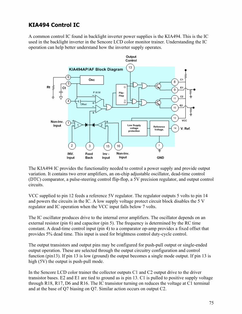
75
KIA494 Control IC A common control IC found in backlight inverter power supplies is the KIA494. This is the IC used in the backlight inverter in the Sencore LCD color monitor trainer. Understanding the IC operation can help better understand how the inverter supply operates.
The KIA494 IC provides the functionality needed to control a power supply and provide output variation. It contains two error amplifiers, an on-chip adjustable oscillator, dead-time control (DTC) comparator, a pulse-steering control flip-flop, a 5V precision regulator, and output control circuits. VCC supplied to pin 12 feeds a reference 5V regulator. The regulator outputs 5 volts to pin 14 and powers the circuits in the IC. A low supply voltage protect circuit block disables the 5 V regulator and IC operation when the VCC input falls below 7 volts. The IC oscillator produces drive to the internal error amplifiers. The oscillator depends on an external resistor (pin 6) and capacitor (pin 5). The frequency is determined by the RC time constant. A dead-time control input (pin 4) to a comparator op-amp provides a fixed offset that provides 5% dead time. This input is used for brightness control duty-cycle control. The output transistors and output pins may be configured for push-pull output or single-ended output operation. These are selected through the output circuitry configuration and control function (pin13). If pin 13 is low (ground) the output becomes a single mode output. If pin 13 is high (5V) the output is push-pull mode. In the Sencore LCD color trainer the collector outputs C1 and C2 output drive to the driver transistor bases. E2 and E1 are tied to ground as is pin 13. C1 is pulled to positive supply voltage through R18, R17, D6 and R16. The IC transistor turning on reduces the voltage at C1 terminal and at the base of Q7 biasing on Q7. Similar action occurs on output C2.

76
Comparator op-amps 1 and 2 internal to the KIA494 serve as protection control for the inverter supply. A resistor divider from the 5V ref. output (pin14) through R10 and R11 set up a threshold voltage at the + inputs (pins 1, 16). Since the resistance of R11 is 1/10 of the resistance of R10, there is about .5V at these pins. Current sensing in the CCFL ground return applies voltage to the – inputs at pin 2 and pin 15. As long as the input voltage exceeds .5volts the op-amps keeps pin 3 low and the PWM internal op-amps permit the oscillator drive to output from the IC. If the voltage to pin 2 or 15 drops below .5 volts the output goes high (pin 3) defeating the output from the IC at pins 8 and 11 stopping operation of the inverter supply. An over-voltage detect circuit(s) also utilize the comparator op-amps 1 and 2 internal to the KIA494. An excessive output raises the detected DC return voltage vial D1 or D7. Over-voltage latch circuits consist of transistor Q11, D9 and C26. A second identical circuit consists of Q11, C25 and D8. When the feedback DC voltage exceeds 18volts, the transistor is biased on reducing pins 15 or 2 to near ground latching the IC output off shutting down the inverter supply.

77
Testing Luminance (Y) Uniformity - ColorPro LCD color monitors contain multiple CCLF lamps typically mounted at the top and bottom rear of the LCD panel. Light dispersion methods conduct and disperse the light as evenly as possible across the entire rear surface of the LCD screen. Although the light dispersion is not perfect its extremely good considering the light all originates at the top and bottom edges of the screen. The uniformity of light across the LCD panel screen is one of the specifications shown in data sheets on the LCD display. A measurement of light intensity emitted from a surface is luminance (Y). Luminance is a light measurement closely related to the human sight characteristic of brightness. It is measured with a U.S measurement in foot lamberts. The foot lambert specifies the amount of light energy, per square foot, emitted from a light source. The CP5000 or CP5001 contains a luminance or Y measurement to measure the level of light emitted from the LCD screen surface. When LCD panels develop a weak, open or defective lamp it is not readily apparent with the visible eye. Because there are multiple bulbs the redundancy means the display continues to be useable. However, the level of luminance or light emitted from one area of the panel becomes significantly different effecting picture quality and brightness. A luminance (Y) measurement is a useful tool in detecting displays with bad CCFL bulbs. For example, a good display typically exhibits 3-6 foot lamberts difference between display points. Points at the display’s top and bottom, at CCFL light origin points, are typically within 1-4 foot lamberts. When a CCFL light is open or weak at the top of the display, the luminance Y values of the bottom of the display are 11-16 foot lamberts greater than the values obtained at the top of the screen. In this manner, a luminance measurement can quickly diagnose a large difference in light output level at the top compared to the bottom caused by a defective CCFL bulb. To detect significant differences in screen luminance values use a test generator and apply a white RASTER pattern across the screen. This produces full light output across the screen surface. Use the ColorPro sensor and CP5000 or CP5001 to measure the luminance (Y= ft. lamberts) at a minimum of 9 test points across the screen surface as shown. Record or note the luminance measurements at the 9 points. Calculate the difference in measurements, especially between the light origin points at the top and bottom of the display. Y 1 = ________ Y 2 = _________ Y 3= _________ Y 4 = ________ Y 5 = _________ Y 6 = _________ Y 7 = ________ Y 8 = _________ Y 9 = _________ Min. Y 1-9 = ________ Max. Y (1-9) = _____ Max – Min = ________ Suggested Activity: Measuring Luminance Uniformity – ColorPro

78
Luminance (Y) Measurements – ColorPro CP5001 Operation of the CP5001 ColorPro is relatively easy. To measure the light emitted from the display, connect the color measurement sensor to the Pocket PC communications port. If the Pocket PC has a serial connection, connect the Null Modem Adapter (39G817) to the DB9 connector. Connect the ColorPro sensor to the other end of the Null Modem Adapter.
Place the color measurement sensor in front of the display screen to measure the emitted light. On a CRT or rear projection display, attach the sensor to the screen, using the tiny suction cups on the sensor to hold it in plae. ColorPro IV The ColorPro IV sensor, the thicker sensor with four light tubes, should be used to measure all LCD flat panel displays. The restricted light acceptance angle of the ColorPro IV sensor, due to the light tubes leading back to the color sensors, allows the sensor to properly integrate the light emitted from a LCD flat panel. Since an LCD flat
panel produces light with a restricted emission angle (similar to an automotive headlight), a sensor with a wide angle integrating diffuser cannot accurately integrate the panel's luminance output. Plus, the chromaticity readings will be inaccurate with a wide angle sensor. The ColorPro IV sensor reads luminance and chromaticity accurately for all LCD flat panel displays.
Navigation & Control of the CP5001 To run the CP5001 ColorPro, connect the color sensor pod to the Pocket PC and double click on the ColorPro CP5001 shortcut icon on the Pocket PC's Program screen. The program will load and initialize the sensor pod. A successful initialization results in a “SETUP” display
screen on the Pocket PC. This screen prompts setup selections that would be made prior to beginning color measurements. See the “Setup Screen” section of this manual. Dark Calibration The CP5001 uses a Dark Calibration procedure to improve the sensor's low light level sensitivity and accuracy. Each time the ColorPro sensor is initialized, the CP5001 prompts you to perform a dark calibration of the sensor. Dark calibration is performed for both the ColorPro III and ColorPro IV sensors. When the attached ColorPro sensor initializes, the Dark Calibration dialog will appear. Place the sensor in the dark (face down on a flat surface, or against your clothing, for example). Then, click the OK button in the dialog window. A ding sound will alert you when the dark calibration

79
is complete, at which point you are free to move the sensor, and the initialization process will complete.
ColorPro Dark Calibration dialog. CP5001 Setup Screen The Setup screen is displayed when “Setup” is selected from within the Setup item on the main menu bar. The Setup screen allows you to define the default measurement settings for the CP5001. These selections are the default settings for which the CP5001 will be configured whenever the program is run. You may change these selections at any time, by opening the Setup screen.
• White Reference - this section allows you to select the chromaticity coordinates to which you wish to calibrate your display. You can select the video industry standard D65, enter your own custom x,y chromaticity coordinates, or select one of 27 CIE standard illuminants or black body color temperature coordinates.
• Comm Port - this section allows you to select USB Port or the Com Port to which the ColorPro sensor will be connected.
• Luminance Units – this section allows you select between two units of measurements used for measuring light illumination by clicking the white button. Foot lamberts or Nits (candelas-per-meter-squared). A black dot identifies the currently selected measurement unit.
• Refresh Rate - this section gives you the option of selecting either Initial Sample, Constant 60Hz, or Constant 50Hz as the method the ColorPro uses for locking to the display refresh rate. Use Constant 60 for LCD Display Panels.
Understanding Measurement Displays The CP5001 offers three choices of measurement displays to assist in color measurements. The choices are Numeric, CIE and Delta RGB. To choose one of these measurement displays, tap on Display in the bottom main menu. Tap on the desired measurement display; either Numeric, CIE or Delta RGB. To start taking measurements in the Numeric Display with the ColorPro, tap the Start button, in the bottom right corner of the screen. The indicator above the Start button will begin flashing green, indicating that the ColorPro is making measurements. To stop taking measurements, tap the Stop button. The indicator will stop flashing and turn red, indicating that the ColorPro is no longer making measurements. Nuumeric display The Numeric display screen provides measurements by providing number values which must be interpreted for determining color temperature. The numbers are based upon the CIE chromaticity chart. The numbers include x, y, K, ∆Exy, and Y. Actual measurement readings, desired reference values and the difference between these are displayed. An explanation of the values display follows.

80
In the Chromaticity section, the large blue numbers on the left display the current readings (labeled Actual). Numeric values include: The x and y values are the 1931 CIE chromaticity coordinates of the measured light. The K value is the Correlated Color Temperature of the measured light. The Reference values or chromaticity coordinates selected in the White Reference Setup. The Difference values are the numeric difference between the reference and actual readings. The ∆Exy value is the delta color error of the measured x, y coordinates, compared to the reference coordinates. This number is derived by the hypotenuse value of the x, y difference, multiplied by 1000. Example – If the x difference is 0.003, and the y difference is 0.004, the x, y hypotenuse would be 0.005. Multiplied by 1000, this gives a ∆Exy value of 5. The bottom portion of the Numeric display includes a Y value readout, White Reference, and Start/Stop control box. The Y value is the luminance value of the measured light. The White Reference (Wht Ref) box shows the white reference chosen in the SETUP screen. This serves as a constant reminder of the target white reference. The Start/Stop button in the lower right of the display provides on/off measurement control. CIE Chromaticity Diagram Display To view measured data in a graphical format corresponding to the CIE Chromaticity Diagram, tap Display on the main menu bar, then tap CIE. The CIE Chromaticity diagram window, displays the measured x, y chromaticity coordinates in the 1931 CIE chromaticity diagram, to assist in calibrating a display to a particular white reference. The colored measurement cursor on the graph represents the actual measured coordinates. The small open box in the center of the graph is the selected White Reference coordinate target. The CIE Chromaticity graph makes color alignments easier to perform by graphically plotting the x, y readings.
The color of the measurement cursor is color-coded to reflect the state of the measurement, as follows:
- Red indicates the measured value is outside the graph range.
- Blue indicates the measured value is inside the graph range.
- Green indicates the measured value is exactly the same as the reference.
The points/axis feature lets you set the graph resolution, in the range of 4-400 points/axis. To change the setting, tap in the box, and type the new value. You may enter 4-400 Points/Axis to set your resolution (graph range). To change the setting, tap in the box, and use the on-screen keyboard to type the new value.

81
The dotted steering lines indicate which direction the measurement will change if the display’s corresponding color is adjusted. Example: If blue is increased, the measurement cursor will travel towards the B indicator, along the path of the dotted line. If blue is decreased, the cursor will travel directly away from the B indicator. Delta RGB Display To view measured data in a graphical format corresponding to amounts of red, green, and blue in the picture, tap Display on the main menu bar, then tap Delta RGB.
The Delta RGB display shows the red, green, and blue color values in a bar graph format. The triangle at the 0 center of the bar graph is the target. Adjusting the bar graphs all to 0 matches the white on the monitor under test to the selected white reference. When using the Delta RGB graph to make a calibration adjustment, one of the three colors is selected as the adjustment reference and the remaining two colors are adjusted to balance with the level of that reference color. Tap the white circle in front of the color you desire to be the reference. Example: In Figure 6, the blue gun is the color reference, the red gun needs to be increased 4% and the green gun needs to be decreased 20% in order to achieve the selected white reference.

82
Inverter power supply symptoms can be typically broken down into the following categories: All Outputs Normal: All Outputs Dead (no output): One Output Low or Missing – Others Normal: All Outputs - Momentary Output Momentary Normal Output one Inverter Side – Other Side No or Low Momentary Output:

83
All outputs normal: If all outputs show normal when viewed on the SC3100 with resistive loads the backlight inverter supply is likely working. If the display exhibits inverter or CCFL symptoms reconnect the CCFL bulbs on one side of the inverter and then the other checking for normal output from the inverter with the SC3100. A problem when connecting CCFL bulbs indicate multiple bad or a shorted CCFL bulb which is shutting down the inverter. If the inverter outputs with the bulbs connected increment the brightness control through its range and monitor the output for PWM shaping by viewing the SC3100 waveform. Normal output and brightness control indicate the backlight supply is working. If the brightness control is not varying the brightness or causing a PWM shaping of the output waveform, test the brightness control input voltage to the inverter input. If it ranges normally, the brightness control circuit of the backlight inverter is defective. If the voltage does not change normally, the microprocessor control or cabling to the inverter is defective. All Outputs Dead (no output): If all the outputs are missing, it is likely that the backlight inverter is missing an input or has a defect in the controller IC common to both output sides. Check the input DC voltage, switch input voltage and brightness control input voltage to the inverter board. If any or all are missing or abnormal the microprocessor/control circuit board or cabling from this circuit board is bad. If all inputs are normal check the DC voltage after the fuse(s). If the voltage is low or missing, the fuse is open. If normal check the voltage, IC oscillator, and drive outputs from the IC as an IC or IC component is likely defective. One Output Low or Missing – Others Normal: This is an unusual symptom as multiple outputs on one side of the inverter share the controller IC, driver, royer oscillator and transformer. Double check the output to be sure. If one output is bad, the problem must be with the series output capacitor, connector or circuit connections to that output. All Outputs - Momentary Output Momentary output(s) is common among backlight inverter symptoms but not to all outputs. A momentary output to all outputs with proper resistive substitute loads suggest the control IC, drivers, royer oscillators, transformers, series output capacitors are all good. The problem is likely a protection shutdown that is unwarranted. The likely cause is a problem in one of the current sense feedbacks or in an over-voltage shutdown protect circuits. Troubleshooting this defect requires measuring the momentary voltages as you turn on the display and output is present for that brief moment. Measure the DC voltage on the DC return test points. Normal voltage suggests a defect in the comparator amplifier section of the control IC or related components. The voltage should rise up to several volts while the output waveform is present. If not, a defect exists in the ground return resistor, diodes, or filter capacitors preventing DC voltage feedback an indication of normal CCFL current flow. Measure for a waveform at the ground return point of the CCFL bulbs to determine where the open is in the DC feedback path.

84
Momentary Normal Output One Inverter Side – Other Side No or Low Momentary Output: An output from one inverter side and not the other is a common symptom. It indicates that a problem exists in the driver, royer oscillator or, transformer on that side of the backlight inverter. Measurements must be made by repeatedly applying voltage to the inverter while you measure momentary waveforms or voltages. Check for the normal waveform at the AMP test points to see if the oscillator is starting and oscillating. A normal momentary waveform indicates a bad transformer or secondary capacitor or connector. No waveform indicates an oscillator defect, driver stage defect or bad IC output. Measure for a momentary waveform at the driver transistor to further isolate the defect. Suggested Activity: Troubleshooting Inverter Power Supply Familiarization Suggested Activity: Troubleshooting Backlight Inverter Power Supply

85
Powering/Testing the Inverter Power Supply with a Bench DC Power Supply In some instances you may suspect that the LCD monitor inputs to the inverter power supply are defective or you must test and troubleshoot the inverter supply board independent of the display. You can power the backlight inverter power supply with a bench DC power supply to test it. You may connect CCFL assemblies to indicate normal output or connect resistor dummy loads and monitor the voltage with the SC3100. All backlight inverter power supplies have a DC input to power the inverter. A common input voltage is 12 volts although some use 5 volts. Connect the power supply positive voltage to the DC power supply input pin of the inverter supply. Connect the power supply negative lead to the ground of the inverter power supply. Note: For connection convenience solder a metal lead clipped from a replacement component to the board trace or back side of the input connector for a sure short-free connection. Don’t be surprised when connected when no current flows as you need to apply a voltage to the switch input. All inverters have a switch input to turn the backlight inverter on or off. This input requires enough voltage to switch on a transistor and subsequently switch the 12 power supply to the inverter circuits. To satisfy the switch input requirements carefully connect a 100-240 K ohm resistor from the DC input to the inverter to the switching input of the inverter. Again you may need to solder a connection lead to the appropriate pin. Once the input is applied to the switched input the inverter supply should turn on and produce a normal output(s) if it is working properly. Caution: The backlight inverter power supply is a high voltage, high frequency supply. Be sure the board is insulated and do not come in contact with the output. A third input to the backlight inverter power supply is for brightness control. You do not need to apply voltage to this input as most designs the brightness is maximum when the brightness input is at its lowest. If you want to test the brightness control input, connect a second DC Bench Power Supply to this input. With the inverter powered and switched on, increase the voltage to the brightness input to approximately 3-4VDC. You should see the brightness of the bulbs decrease or output voltage PWM duty-cycle change on the SC3100 monitoring the output.

86
Suggested Activity: Powering/Testing the Inverter Power Supply with a Bench DC Power Supply

87
Finding Replacement CCFLs or Inverter Power Supplies There are several suppliers of CCFL replacement bulbs and inverter power supply modules. It is likely that more sources will become available as LCD color displays become more popularity and the desire to extend the useful life of many of these display increase. Manufacturers of the display are an excellent source for replacement parts. Here are some examples of some additional suppliers. Endicott Research Group Inc. is a manufacturer of backlight inverter power supplies. They offer replacement inverters for most LCD modules. A complete list of inverter replacements may be obtained at www.ergpower.com Another example of a source for backlight inverter power supplies is Applied Concepts Inc. www.acipower.com They offer replacement backlight inverter power supplies for LCD modules. Assistance is available on their website. More sources are available by searching the world wide web. CCFL Sources: A large manufacture of CCFL lamps is JKL Components Corp. They offer a large selection of replacement lamps. More information is available at www.jkllamps.com or 1-800421-7244. Other parts suppliers offer JKL lamps including DigiKey and Mouser Electronics Moniserv is a computer monitor repair depot that offers LCD panel repair and offers replacement CCFL lamps, CCFL assemblies, and inverter power supplies. See www.moniserv.com Replacing CCFFs or CCFLs Assemblies
CCFL assembly in Philips LM181 LCD panel Replacing CCFL bulbs or assemblies differs between LCD panels. In some panels the CCFL assembly can be removed without LCD panel disassembly. The CCFL assembly slides out the edge of panel. Other LCD panels must be disassembled to gain access to the CCFL bulbs. The following activity contains a pictorial on LCD panel disassembly (Philips LM181-06) to replace the CCFL bulb or assembly. Suggested Activity: Replacing the CCFL – Philips LM181E06 LCD Panel
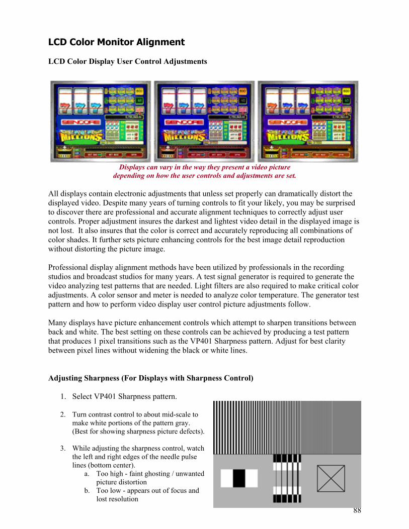
88
LCD Color Monitor Alignment LCD Color Display User Control Adjustments
Displays can vary in the way they present a video picture depending on how the user controls and adjustments are set.
All displays contain electronic adjustments that unless set properly can dramatically distort the displayed video. Despite many years of turning controls to fit your likely, you may be surprised to discover there are professional and accurate alignment techniques to correctly adjust user controls. Proper adjustment insures the darkest and lightest video detail in the displayed image is not lost. It also insures that the color is correct and accurately reproducing all combinations of color shades. It further sets picture enhancing controls for the best image detail reproduction without distorting the picture image. Professional display alignment methods have been utilized by professionals in the recording studios and broadcast studios for many years. A test signal generator is required to generate the video analyzing test patterns that are needed. Light filters are also required to make critical color adjustments. A color sensor and meter is needed to analyze color temperature. The generator test pattern and how to perform video display user control picture adjustments follow. Many displays have picture enhancement controls which attempt to sharpen transitions between back and white. The best setting on these controls can be achieved by producing a test pattern that produces 1 pixel transitions such as the VP401 Sharpness pattern. Adjust for best clarity between pixel lines without widening the black or white lines. Adjusting Sharpness (For Displays with Sharpness Control)
1. Select VP401 Sharpness pattern.
2. Turn contrast control to about mid-scale to make white portions of the pattern gray. (Best for showing sharpness picture defects).
3. While adjusting the sharpness control, watch
the left and right edges of the needle pulse lines (bottom center).
a. Too high - faint ghosting / unwanted picture distortion
b. Too low - appears out of focus and lost resolution

89
The top, multi-burst section of the Sharpness pattern can also be used as a reference to adjust the sharpness control. Starting with the sharpness control at its minimum setting, increase the control until all five bursts are at equal brightness levels, but not high enough to cause ghosting lines adjacent to the widest multi-burst stripes at the left or widening of the fine detail lines 1 section from the right. Black Level Adjustment: The black level control changes the level of the video that represents black. An improper setting results in near dark picture portions becoming black and no longer visible.
1. To accurately set the Black Level, select the High Low Tracking (HiLo Trk pattern on the VP401.
2. Pay attention to the top black section in
the middle where a 5% and 2.5% box exist. Increase the black level control until the inner 5% and 2.5% boxes disappear.
3. Decrease the black level control until the
inner two boxes are visible. Inner box is 5% above black.
Outer box is 2.5% above black. Note: In some displays the black level adjustment may respond in the opposite manner. Strive to achieve a setting in which the 5% and 2.5% boxes are just discernable. You may have difficulty setting black level to achieve a visible 5% and 2.5% boxes on some LCD displays. Selecting a Linear Gamma selection vs. CRT gamma can improve black level. Setting higher red, green, blue settings in the user color temperature adjustment can also improve black level. Contrast Adjustment:
1. Select the High Low Tracking (HiLo Trk) video pattern on the VP401.
2. Select VP40x HiLo Trk (HIGH/LOW TRACK)
3. Pay attention to the white portion of the
screen (bottom) as you increase the contrast control:
a. Notice how both 97.5% & 95% white boxes disappear as you increase the control.
b. Contrast is accurately set when it is at the maximum setting yet both boxes are still clearly visible.
Outer box is 97.5 white. Inner box is 95% white.

90
Brightness Adjustment – LCD Monitors: The brightness control in an LCD Color Monitor controls the brightness or intensity of the light produced by the backlight CCFL in the LCD panel. The brightness control adjusts the output of the backlight inverter power supply.
1. To check the brightness control, select the HiLo Trk pattern on the VP401.
2. Adjust the brightness control to achieve satisfactory brightness. Be sure the 2.5%, 5%, 95% and 97.5% boxes remain visible.
Note: In most LCD monitors the brightness control has little or no effect on the discernable center black or white boxes in the HiLo Trk pattern. If so, you may set the brightness control to a level that maintains correct color level and tint. To match settings on multiple displays in a test console or casino floor, use the Y or luminance light level reading provided by the CP5000. Adjust the brightness control for a reference Y level using the RASTER pattern of the VP401. (Note: Higher settings – higher CCFL lamp currents reduce usable life hours on bulbs)
2.5% and 5% above black boxes
95% and 97.5% white boxes

91
Alternative Brightness Control Adjustment (Use for displays with typical brightness controls – not applicable for many LCD monitors)
1. To adjust the brightness control, select the PLUGE pattern on the VP401.
Note: The ambient room light affects the discernable level for setting brightness.
2. Watch the second box from the inside. This box is alternating between 7.5 IRE and 0 IRE
(black and blacker-than-black).
3. Adjust the User Brightness control until the 7.5 IRE and 0 IRE levels appear the same and no flashing can be seen. The outer 10 IRE box should still be slightly visible.
Adjusting Color Saturation, Hue, Skin Tone Color Saturation/Level Adjustment:
1. Select the SMPTE Color Bars pattern on the VP401.
2. Adjust the Color Level or Color Saturation control from one end of its adjustment range
to the other. What effect does this control have on the picture?
NTSC 0 / 7.5 IRE 7.5 IRE 10 IRE 7.5 IRE
HDTV 0 /- 4 IRE 0 IRE 10 IRE 0 IRE
Top Outside Bar
Small Center Bar Small Center Bar
Large Outside Bar

92
3. View the color pattern through the blue filter as you adjust the color control. Pay special
attention to the large top outside blue and white bars and the small bars below them (see illustration below).
4. While viewing the pattern through the blue filter, adjust the Color control to make these
bars appear to have the same intensity (brightness) level. Alternate Saturation/Level Adjustment – Recommended: The Decod Adj. test pattern contains three primary color sections. Each primary section includes a white reference bar and secondary color bars in an alternating pattern of six bars. The two secondary color combinations result from mixing the primary color and each of the other two primaries. Use by looking through the matching color filter to remove the primary color.
1. Select the Decod Adj. Pattern on the VP401.
2. Looking through the Blue Filter concentrate on the bottom blue section where the cyan
and magenta sections intersect.
3. Adjust the Color Saturation/Level user control until the cyan and magenta sections appear to have the same intensity (brightness) level.
Note: You will see these sections alternate from lighter to darker as you cross over the correct adjustment point.
cyan/magenta intersect
93
Color Hue/Tilt Adjustment: Hue/Tint Control
1. Select the SMPTE Color Bars pattern on the VP401.
2. Adjust the Tint/Hue control from one end of its adjustment range to the other.
3. What effect does this control have on the picture?
4. View the color pattern through the blue filter as you adjust the Tint/Hue control. Pay
special attention to the Cyan/Magenta bars that are located above and below one another (see illustration below).
5. While viewing the pattern through the blue filter, adjust the Tint/Hue control to make
these bars appear to have the same intensity (brightness) level. Alternative Hue/Tint Adjustment Method – Recommended:
1. Select the Decod Adj Pattern on the VP401.
2. Looking through the Blue Filter concentrate on the top of the blue section where the blue
outer section intersects the white stripe above the cyan/magenta stripes.
3. Adjust the Hue/Tint control until the blue and white sections appear to have the same intensity (brightness) level.
Color Skin Tone Adjustment:
Cyan
Magenta
Magenta Cyan
Blue
White

94
Some LCD displays improve color performance by offering a color skin tone adjustment. This adjustment provides digital level shifts to red to improved color reproduction so it more closely matches color reproduction compared to other display technologies.
1. To accurately set the Color Skin Tone adjustment, select the Decod Adj. Pattern on the VP401.
2. Looking through the red filter concentrate on the top of the red section where the
magenta and yellow sections intersect.
3. Adjust the Color Skin Tone user control until the magenta and yellow bars have the same intensity (brightness) level.
Setting the Phase Adjustment The phase of the analog to digital converter in an LCD display can be electronically adjusted. Adjusting the phase provides improved picture display resolution as it lines-up the LCD display’s A/D sample time with the pixel transition time of the incoming signal. Procedure: Use a test signal generator that produces a 1 pixel transition in the native resolution of the display. Use the display’s native resolution SXGA 1280X1024 60Hz as the generator signal format. Use a test pattern on the generator with 1 pixel transitions.
1. Input a test signal to the LCD display’s VGA input. 2. Set the VP401 to the VESA/Mac –RGB signal type, 1280x1024 60Hz, and select the
Sharpness pattern. use the Multiburst pattern or Sharpness pattern.
3. Select the Phase adjustment on the LCD Monitor Trainer.
4. Vary the Phase control until the resolution is the clearest in the 1 pixel transition portion of the Multiburst (top right) section of the Sharpness pattern.
Note: There may be several position of the control range that produce a good alignment. Select the control position nearest the center of the range.
Adjust Phase for Clearest transitions
Magenta – yellow intersections
95
Color Display Calibration Basics All color video display devices share one critical calibration – color balance. This is true whether the device displays standard NTSC signals, standard computer format signals, proprietary high resolution signals, or HDTV signals. To display the most accurate colors, any video display’s color balance must be adjusted to match the color balance of the signal source. This exact balance of red, green, and blue to make exactly the right color of white and neutral grays in the picture (often called White Balance) must be correct in both low brightness and high brightness parts of the picture. To understand how we see, specify, and measure this color balance, let’s review some basics of light and color. Human Sight Characteristics Light is electromagnetic energy within a narrow range of frequencies that are higher frequency than microwaves, but lower frequency than x-rays. Each different frequency (or wavelength) of light energy, if seen by itself, is perceived by the human eye/brain as a different, fully saturated, color. In a certain respect, the eye/brain acts like a tuned, high frequency radio receiver.
The human eye sees energy in a small slice of the electromagnetic spectrum as visible light. Three characteristics define the way the human eye/brain sees light that is either radiated from or reflected off an object. Brightness: The eye sees the total amount of light energy radiated or reflected by an object, in comparison to other light sources or lighted objects in the field of view, as the brightness of the object. Saturation: A single frequency of light, at any energy level, is seen as a fully saturated, vivid color. The saturation of that color decreases as any other light frequency, or any combination of light frequencies, is added to the original light. If equal energy of all visible light frequencies is added together, the result is zero saturation, pure white light. Hue: For any combination of light energy other than pure white, the dominant perceived frequency of the combined light energy is known as the hue of the light.

96
The human eye perceives light energy in terms of its hue, saturation, and brightness.
Light Measurement To specify different amounts and combinations of light energy, we would like to measure light in a way that corresponds closely to the way we see light. In the video display industry, two types of measurement units are used to measure light and relate it to the human sight characteristics. These two measurement units are luminance and chromaticity. Luminance is a type of light measurement closely related to the human sight characteristic of brightness. The footlambert is the U.S. measurement unit of luminance. It specifies the number of lumens of light energy emitted from each square foot of a light source, such as a video display, or reflected off a solid object. (Footcandles, on the other hand, are a measurement unit of illuminance, the light falling on an object.) Chromaticity is a type of light measurement related to the human sight characteristics of hue and saturation. This combined method of chromaticity measurement was developed by the C.I.E. (International Commission on Illumination) in 1931 and is used by the video industry for all display color measurements. The C.I.E. developed a chromaticity diagram which graphically depicts the relationship between the hue and saturation of light sources. The C.I.E. Chromaticity Diagram plots the pure spectral colors (hues) around the curved border (380-780 nm). The results of mixing any of these fully saturated spectral colors are shown at the base and interior of the diagram. Any visible color can be specified by the x coordinate and the y coordinate position of that color on the diagram. The 1931 C.I.E. Chromaticity Diagram provides a convenient tool for easily specifying the hue and saturation of any visible color. Video Display White Reference The C.I.E. coordinate pair of x = 0.333, y = 0.333 (E) specifies the white light produced by mixing equal light energy of all wavelengths (zero saturation). The color of any point immediately surrounding the equal energy white point would also appear white, if seen by itself with no other color reference. It would seem logical that equal-energy white (E) would be used as the standard color of white for video display systems. However, since a more bluish white appears brighter, the C.I.E. coordinate pair of x = 0.313, y = 0.329 (C.I.E. standard illuminant D65) is the white color which was chosen as the standard white reference for all video and computer display systems. This allows displays to appear brighter without producing additional light energy output, yet doesn’t shift the color of white enough to be detrimental to color accuracy.

97
White from Red, Green, and Blue On the C.I.E. chromaticity diagram, if any three color points are chosen, the area included by the connecting triangle represents the range of colors that are able to be produced by mixing the three chosen colors. The three points are known as the primary colors. The connecting triangle encloses the full range of colors (gamut) which is able to be produced by a display that produces mixtures of those colors of red, green, and blue light. A triangle formed by any three colors encloses all the colors able to be formed by mixing the three colors. The Eye - A Tristimulus Device The human eye sees light through rod and cone type light receptors. There are red, green, and blue cone type receptors that give us color vision. The rod receptors give us black and white vision, especially in small detail and low light. Three types of cone receptors in our eye provide response to light in the red, green, and blue portions of the visible spectrum. The red, green, and blue cone receptors each have a different response to different colors (frequencies) of light. The average response of the human eye receptors to light across the visible spectrum is shown by the Standard Observer Response graph, developed by the International Commission on Illumination (C.I.E.). The C.I.E. Standard Observer Response graph shows the relative sensitivity of each type cone at different light frequencies. We call this tristimulus vision, as there are three types of receptors that individually send information to our brain and allow us to perceive different colors for the different mixtures of light energy within the visible spectrum.

98
Tristimulus Measuring Devices Tristimulus color measurement devices are called colorimeters. This type of device works very much the same way as the human eye. Three filtered light sensors receive light from the source to be measured. The filter for each light sensor allows only a certain amount of each color of light to reach the sensor. The response of each of the three filters is designed to mimic the response of one of the types of cones in the average human eye. The three light sensors in a colorimeter receive filtered light with responses equal to that of the human eye. The measurement information from each of the three light sensors is the same as the information from each of the three types of cones in the eye, only in electronic signal form. This information allows us to compute a different measurement result for the different mixtures of light energy within the visible spectrum, in a way that duplicates the response of the human eye/brain combination. To accurately predict the response of the human eye to a combination of light energy at different frequencies, a tristimulus color measurement device must “see” light exactly the same way the human eye sees light, as documented by the C.I.E. Standard Observer Response graph. Display Technology Challenges The new display types that are now on the market (plasma, LCD, DLP, LCOS, D-ILA, etc.) each produce light energy with a spectral power distribution (SPD) that is usually very different from the average spectrum produced by CRTs. This is a change from when we worked only with direct-view CRTs, as all CRT phosphor sets produced strong peaks of light and low levels of light at pretty much the same color frequencies. Some of the new display types produce strong peaks of light at color frequencies where CRTs produce very little light. Each of the new display types is still able to produce a standard color of white by adjusting the relative balance of colors in the red, green, and blue portions of the spectrum.
Courtesy Joe Kane Productions Different display technologies each have a unique spectral power distribution (SPD). Because the new technology displays may produce strong peaks of light at just about any color frequency, it is now critical that a colorimeter’s optical filters must accurately duplicate the CIE standard observer response at all color frequencies, not just at the particular frequencies at which direct-view CRTs produce high light output. Its three color sensors must see light over the entire visible spectrum with the exact same amplitude response as the three color sensors of our eye.

99
The response of a colorimeter’s optical filters (white) needs to be accurate at all color frequencies to accurately measure light from any type of display. If a colorimeter uses optical filters which are accurate to the human eye response at all frequencies of light, not just high output CRT frequencies, the instrument will accurately measure all displays of the past, present, and future, no matter what their SPD. All-Display Color Analyzer The Sencore CP5000 'ColorPro' uses optical filters which are accurate to the C.I.E. standard observer response at all frequencies of light. This economical measurement system allows you to measure and calibrate any video display (LCD, DLP, Plasma, CRT, and any future technology), confident that you've accurately aligned it to industry standards and made the display deliver its peak performance. The continuously-updated CP5000 readings provide display alignment capabilities not available with the single-shot readings provided by more expensive spectroradiometers (which are also very accurate). A user-friendly graphical interface speeds display calibration time with simple, easy to follow measurement screens that show you exactly what to adjust to obtain a perfect match to the industry standard white reference. Integrated software lets you store a display’s calibration data and print a customized, easily understood calibration report.

100
3200 Sencore Drive 1.800.736.2673 Sioux Falls, SD 57107 1.605.339.0100 http://www.sencore.com mailto:[email protected] Printed in U.S.A.