handling of thin silicon wafers in pv manufacturingon wafer stresses, distortion and breakage....
TRANSCRIPT
PV Industry Needs Workshop February 2, 2006
Handling of Thin Silicon Wafers in PV Manufacturing
Xavier Brun and Shreyes N. Melkote**Assoc. Professor & Woodruff Faculty Fellow
George W. Woodruff School of Mechanical Engineering &
Manufacturing Research CenterGeorgia Institute of Technology
Atlanta, Georgia
PV Industry Needs Workshop February 2, 2006
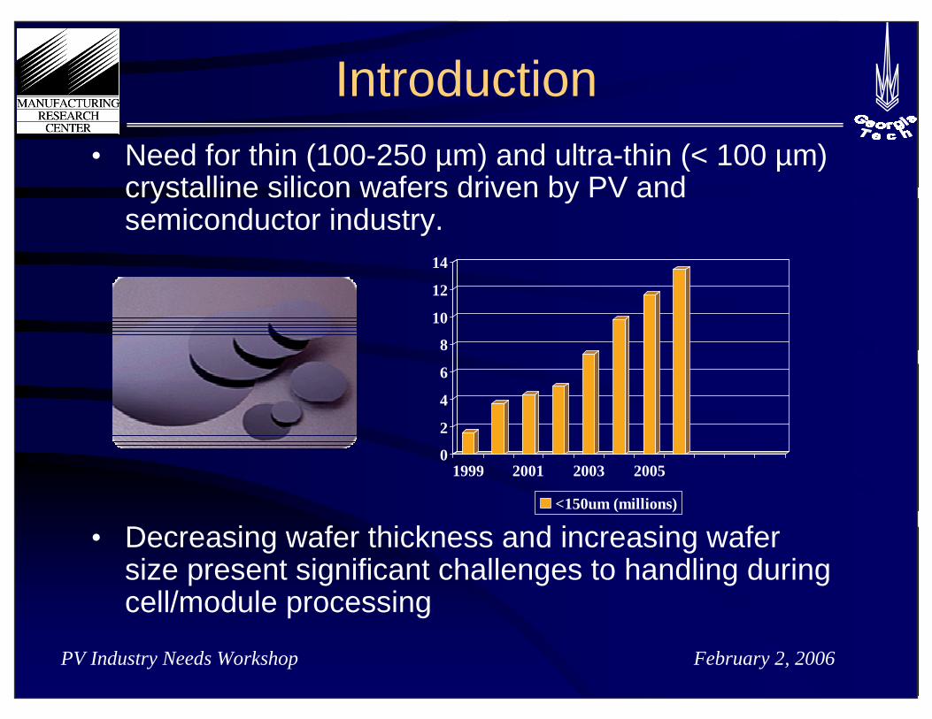
Introduction• Need for thin (100-250 µm) and ultra-thin (< 100 µm)
crystalline silicon wafers driven by PV and semiconductor industry.
• Decreasing wafer thickness and increasing wafer size present significant challenges to handling during cell/module processing
0
2
4
6
8
10
12
14
1999 2001 2003 2005
<150um (millions)
PV Industry Needs Workshop February 2, 2006
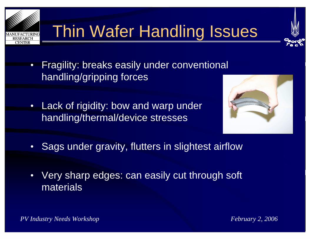
Thin Wafer Handling Issues
• Fragility: breaks easily under conventional handling/gripping forces
• Lack of rigidity: bow and warp under handling/thermal/device stresses
• Sags under gravity, flutters in slightest airflow
• Very sharp edges: can easily cut through soft materials
PV Industry Needs Workshop February 2, 2006
Potential Solutions
• Re-design/optimization of existing wafer holding devices/techniques through modeling and analysis
• Minimize wafer handling/transfer via design of integrated wafer processing equipment and/or “palletized” wafer transfer systems
• Develop non-contact handling methods e.g. air conveyors

PV Industry Needs Workshop February 2, 2006
Research Objectives
Ø Investigate influence of gripper and wafer characteristics on wafer stresses, distortion and breakage. Bernoulli, Vacuum and Mechanical grippers will be studied.
Ø Investigate interaction of process induced residual stresses with handling stresses
Ø Optimize gripper variables to minimize breakage and hence improve yield of thin crystalline silicon wafers in solar cell fabrication
PV Industry Needs Workshop February 2, 2006
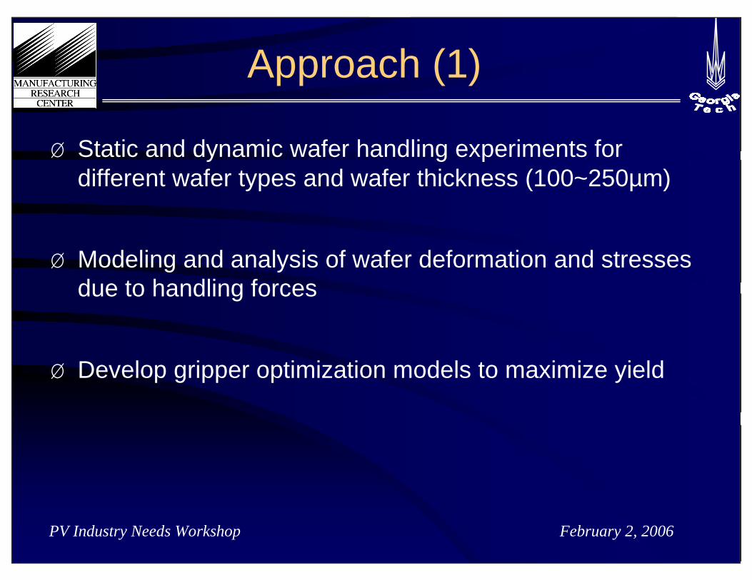
Approach (1)
Ø Static and dynamic wafer handling experiments for different wafer types and wafer thickness (100~250µm)
Ø Modeling and analysis of wafer deformation and stresses due to handling forces
Ø Develop gripper optimization models to maximize yield

PV Industry Needs Workshop February 2, 2006
Approach (2)
Ø Methodology for understanding the impact of handling and residual stresses on wafer breakage
Measure residual stresses in the
wafer
Calculate handling stresses
Compare with breakage stress
Polariscope-based residual stress measurement system
Pressure and Deformation models
Fracture strength Data
Superpose residual and
handling stresses
Wafer Processing
PV Industry Needs Workshop February 2, 2006
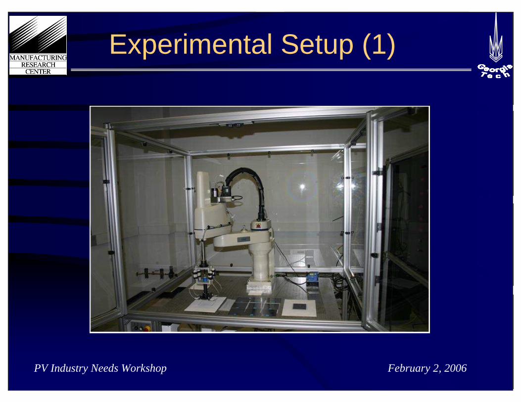
Experimental Setup (1)
PV Industry Needs Workshop February 2, 2006
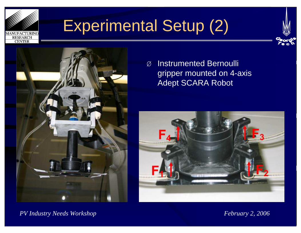
Ø Instrumented Bernoulli gripper mounted on 4-axis Adept SCARA Robot
Experimental Setup (2)
PV Industry Needs Workshop February 2, 2006
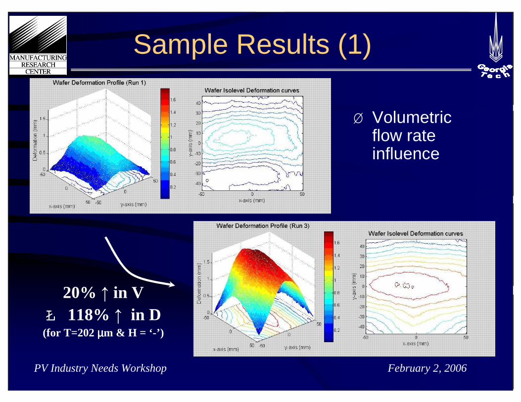
Sample Results (1)
Ø Volumetric flow rate influence
20% in V ŁŁŁŁ 118% in D(for T=202 µµµµm & H = ‘-’)

PV Industry Needs Workshop February 2, 2006
Sample Results (2)
Ø Thickness influence
43% in T ŁŁŁŁ 50% in D
(for V= 39.1 lpm & H=‘-’)
PV Industry Needs Workshop February 2, 2006
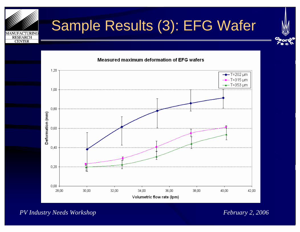
Sample Results (3): EFG Wafer

PV Industry Needs Workshop February 2, 2006
Modeling & Analysis (1)
Ø Methodology for modeling and analysis of deformation and stresses in thin wafer held by Bernoulli gripper
ri
ro
h
hi
re
Cone Mill
Separation
( ) )()(2
1)( 22
0 rEfrvvprp a +−=− ρ
∫= 0
)()(r
rdrrdEfrEf
2
2
3
)(
81
)(
16)(
r
rhQK
rhr
QrdEf ×+×=
νππνρ
PV Industry Needs Workshop February 2, 2006
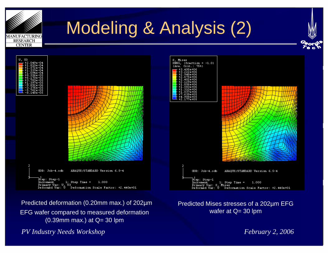
Modeling & Analysis (2)
Predicted deformation (0.20mm max.) of 202µm
EFG wafer compared to measured deformation(0.39mm max.) at Q= 30 lpm
Predicted Mises stresses of a 202µm EFG wafer at Q= 30 lpm

PV Industry Needs Workshop February 2, 2006
Modeling & Analysis (3)
PV Industry Needs Workshop February 2, 2006
Summary
Ø Research focus on developing fundamental understanding of thin wafer handling issues
Ø Evaluate capabilities and limitations of current handlingdevices for thin silicon wafers e.g. Bernoulli, vacuum, mechanical grippers
Ø Analyze interaction of residual stresses and handlingstresses
Ø Develop physics-based models for thin wafer handlingoptimization to minimize breakage

PV Industry Needs Workshop February 2, 2006
Acknowledgments
Ø NREL
Ø Schott Solar
Ø Manz Automation