h20 hsupa pci express mini card module - radiosurplus … h20.pdf · · 2017-06-201.1 description...
TRANSCRIPT
D
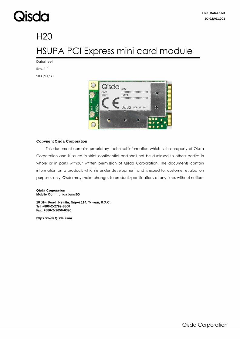
H20 HSUPA PCI Express mini card module
Datasheet
Rev. 1.0
2008/11/30
Copyright Qisda Corporation
This document contains proprietary technical information which is the property of Qisd
Corporation and is issued in strict confidential and shall not be disclosed to others parties
whole or in parts without written permission of Qisda Corporation. The documents conta
information on a product, which is under development and is issued for customer evaluatio
purposes only. Qisda may make changes to product specifications at any time, without notice
Qisda Corporation Mobile Communications BG 18 JiHu Road, Nei-Hu, Taipei 114, Taiwan, R.O.C. Tel: +886-2-2799-8800 Fax: +886-2-2656-6390 http://www.Qisda.com
atasheet H20 Datasheet9J.0JA01.001
a
in
in
n
.

HISTORY
Version Date Notes
VER: 1.0 2008-NOV-30 FIRST RELEASE
1. INTRODUCTION.......................................................................................................................................................................... 4
1.1 Description....................................................................................................................................................4
1.2 Application Device......................................................................................................................................4
2. FEATURES .................................................................................................................................................................................... 5
2.1 General Characteristics..............................................................................................................................5
2.2 RF Functionalities..........................................................................................................................................6
3. HARDWARE DESCRIPTION....................................................................................................................................................... 10
3.1 System Interface ........................................................................................................................................10
3.2 Functional Diagram ...................................................................................................................................11
3.3 Pin Description............................................................................................................................................12
3.4 Terminal Definition .....................................................................................................................................14
3.5 Electrical Characteristics ......................................................................................................................................... 16
3.6 Environmental ............................................................................................................................................23
3.7 Physical Package......................................................................................................................................24
4. SOFTWARE CHARACTERISTICS................................................................................................................................................ 27
4.1 Introduction ................................................................................................................................................27
4.2 Software Architecture................................................................................................................................27
4.3 HSPA Modem Application ........................................................................................................................29

1. INTRODUCTION
1.1 Description
Overview
This document describes all the functions, features, and interfaces of the HSUPA PCI
Express Mini Card Module – H20 from Qisda. Qisda H20 HSUPA module supports Tri-band
WCDMA/HSDPA/HSUPA and Quad-band GSM/GPRS/EDGE network connection capability.
Qisda H20 HSUPA card can provides high speed data connection, the data speed of
downlink and uplink path is up to 7.2Mbps and 5.76Mbps respectively .Furthermore, users can
ease to use this module by using the “HSPA Modem” application software that we provide for
Windows XP and Vista system.
With the Qisda H20 HSUPA module, devices are enhanced in both functionality and
usability based on state of the art wireless technology.
1.2 Application Device
Scope
Qisda H20 module is a high speed modem card with PCI Express minicard form factor
and is focusing on the Notebook, UMPC, MID and other portable device marketing.
Notebook
Ultra Mobile PC
Mobile Internet Device
Wireless Router

2. FEATURES
2.1 General Characteristics
Bands:
Tri Band WCDMA and Quad Band GSM
Band TX RX
GSM850 824~849 MHz 869~894MHz
EGSM900 880~915 MHz 925~960MHz
DCS1800 1710~1785MHz 1805~1880MHz
PCS1900 1850~1910MHz 1930~1990MHz
WCDMA850 824~849 MHz 869~894MHz
WCDMA1900 1850~1910MHz 1930~1990MHz
WCDMA2100 1920~1980MHz 2110~2170MHz
Support SIM Interface: 1.8V/3V
Form factor
i. Dimension: 50.95 x 30 x 5.0 mm
ii. Weight: 12g
Power
Operation Voltage: 3.3V +/- 9%
Power Consumption:
Data Mode:
Band Typ Max Unit
GSM850 / PCL=5 360 390 mA
EGSM900 / PCL=5 360 390 mA
DCS / PCL=0 310 340 mA
PCS / PCL=0 310 340 mA
WCDMA (all band) 750 820 mA
EDGE & GPRS Multislut:
GMSK 8PSK
Band Slot 1 Slot 2 Slot 3 Slot 4 Slot 1 Slot 2 Slot 3 Slot 4
GSM850 < 380mA <635mA < 755mA < 775mA < 280mA < 310mA < 425mA < 505mA
GSM900 < 380mA < 635mA < 755mA < 775mA <280mA <310mA < 425mA < 380mA
DCS1800 < 330mA < 525mA < 610mA < 640mA < 200mA < 305mA < 340mA < 375mA
PCS1900 <330mA < 525mA < 610mA < 640mA < 200mA < 305mA < 340mA < 375mA

Sleeping Mode:
Typ (Average) Max (Average) Unit
GSM / MFRM=2 5 6 mA
GSM / MFRM =9 3 4.5 mA
DCS / MFRM =2 5 6 mA
DCS / MFRM =9 3.4 5 mA
PCS / MFRM =2 5 6 mA
PCS / Page frame=9 3.1 4.5 mA
WCDMA / DRX=6 (0.64 S) 5.7 5.5 mA
WCDMA / DRX=9 (5.12 S) 3.2 4.5 mA
Shutdown current 0.1 1 uA
Hardware Interface:
52 Pins PCI Express Mini Card connector interface
2 RF Antenna Coaxial Connectors
Software Interface:
USB driver
HSPA Modem software tool.
2.2 RF Functionalities
Maximum TX Power
The performance of the transmitter meets test requirement ETSI TS 151 010-1 chapter 13.3 for
GSM, chapter 13.17.3 for EDGE and TS 34.121 chapter 5.2&5.4.3 for WCDMA, chapter 5.2A for
HSDPA, chapter 5.2B for HSUPA.
Band Max Min
GSM850 33 dBm ±2dBm 5 dBm ±5dBm
EGSM 33 dBm ±2dBm 5 dBm ±5dBm
DCS 30 dBm ±2dBm 0 dBm ±5dBm
PCS 30 dBm ±2dBm 0 dBm ±5dBm
GSM850(EDGE) 27 dBm ±3dBm 5 dBm ±5dBm
EGSM(EDGE) 27 dBm ±3dBm 5 dBm ±5dBm
DCS(EDGE) 26 dBm ±3dBm 2 dBm ±5dBm
PCS(EDGE) 26 dBm ±3dBm 2 dBm ±5dBm
UMTS-2100 24 dBm +1/-3dBm Less than -50dBm
UMTS-1900 24 dBm +1/-3dBm Less than -50dBm
UMTS-850 24 dBm +1/-3dBm Less than -50dBm
1/15≦βo/βd≦12/15 (HS-DPCCH) 24 dBm +1/-3dBm
13/15≦βo/βd≦15/8 (HS-DPCCH) 23 dBm +2/-3dBm
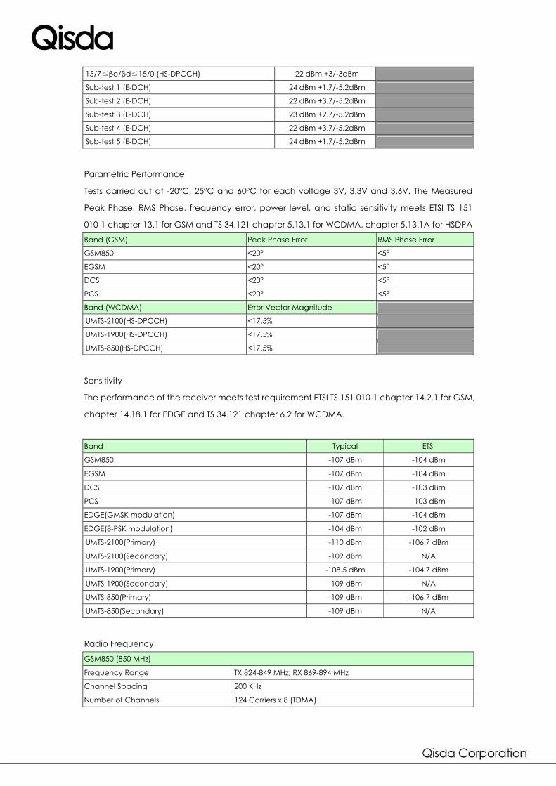
15/7≦βo/βd≦15/0 (HS-DPCCH) 22 dBm +3/-3dBm
Sub-test 1 (E-DCH) 24 dBm +1.7/-5.2dBm
Sub-test 2 (E-DCH) 22 dBm +3.7/-5.2dBm
Sub-test 3 (E-DCH) 23 dBm +2.7/-5.2dBm
Sub-test 4 (E-DCH) 22 dBm +3.7/-5.2dBm
Sub-test 5 (E-DCH) 24 dBm +1.7/-5.2dBm
Parametric Performance
Tests carried out at -20ºC, 25ºC and 60ºC for each voltage 3V, 3.3V and 3.6V. The Measured
Peak Phase, RMS Phase, frequency error, power level, and static sensitivity meets ETSI TS 151
010-1 chapter 13.1 for GSM and TS 34.121 chapter 5.13.1 for WCDMA, chapter 5.13.1A for HSDPA
Band (GSM) Peak Phase Error RMS Phase Error
GSM850 <20° <5°
EGSM <20° <5°
DCS <20° <5°
PCS <20° <5°
Band (WCDMA) Error Vector Magnitude
UMTS-2100(HS-DPCCH) <17.5%
UMTS-1900(HS-DPCCH) <17.5%
UMTS-850(HS-DPCCH) <17.5%
Sensitivity
The performance of the receiver meets test requirement ETSI TS 151 010-1 chapter 14.2.1 for GSM,
chapter 14.18.1 for EDGE and TS 34.121 chapter 6.2 for WCDMA.
Band Typical ETSI
GSM850 -107 dBm -104 dBm
EGSM -107 dBm -104 dBm
DCS -107 dBm -103 dBm
PCS -107 dBm -103 dBm
EDGE(GMSK modulation) -107 dBm -104 dBm
EDGE(8-PSK modulation) -104 dBm -102 dBm
UMTS-2100(Primary) -110 dBm -106.7 dBm
UMTS-2100(Secondary) -109 dBm N/A
UMTS-1900(Primary) -108.5 dBm -104.7 dBm
UMTS-1900(Secondary) -109 dBm N/A
UMTS-850(Primary) -109 dBm -106.7 dBm
UMTS-850(Secondary) -109 dBm N/A
Radio Frequency
GSM850 (850 MHz)
Frequency Range TX 824-849 MHz; RX 869-894 MHz
Channel Spacing 200 KHz
Number of Channels 124 Carriers x 8 (TDMA)

Modulation GMSK / 8-PSK
Duplex Spacing 45 MHz
Frequency Stability +/- 0.1 ppm (Uplink TX)
Power Output 33 dBm Class 8 (2 W peak) – 5 dBm
Output Impedance 50 Ohm
Spurious Emission -36 dBm up to 1 GHz (< -30 dBm > 1 GHz)
EGSM (900 MHz)
Frequency Range TX 880-915 MHz; RX 925-960 MHz
Channel Spacing 200 KHz
Number of Channels 124 Carriers x 8 (TDMA)
Modulation GMSK / 8-PSK
Duplex Spacing 45 MHz
Frequency Stability +/- 0.1 ppm (Uplink TX)
Power Output 33 dBm Class 8 (2 W peak) – 5 dBm
Output Impedance 50 Ohm
Spurious Emission -36 dBm up to 1 GHz (< -30 dBm > 1 GHz)
DCS (1800 MHz)
Frequency Range TX 1710-1785 MHz; RX 1805-1880 MHz
Channel Spacing 200 KHz
Number of Channels 374 Carriers x 8 (TDMA)
Modulation GMSK / 8-PSK
Duplex Spacing 95 MHz
Frequency Stability +/- 0.1 ppm (Uplink TX)
Power Output 30 dBm – 0 dBm
Output Impedance 50 Ohm
Spurious Emission -36 dBm up to 1 GHz (< -30 dBm > 1 GHz) Compatible with phase 2 feature
PCS (1900 MHz)
Frequency Range TX: 1850~1910MHz; RX: 1930~1990MHz
Channel Spacing 200KHz
Number of Channels 299 Carriers x 8 (TDMA)
Modulation GMSK / 8-PSK
Duplex Spacing 80 MHz
Frequency Stability +/- 0.1 ppm (Uplink TX)
Power Output 30 dBm – 0 dBm
Output Impedance 50 Ohm
Spurious Emission -36 dBm up to 1 GHz (< -30 dBm > 1 GHz) Compatible with phase 2 feature
WCDMA_IMT (2100 MHz)
Frequency Range TX: 1920~1980MHz; RX: 2110~2170MHz
Channel Raster 200KHz
Number of Channels 299 Carriers x 8 (TDMA)
Modulation QPSK
Duplex Spacing 190 MHz
Frequency Stability +/- 0.1 ppm (Uplink TX)
Power Output 24 dBm +1/-3dBm - less than -50dBm
Output Impedance 50 Ohm
Spurious Emission -67dBm(925-935MHz);-79dBm(935-960MHz);-71dBm(1805-1880MHz) ;-60dBm(1845-1880MHz);-41dBm(1885-1920MHz)

WCDMA_PCS (1900 MHz)
Frequency Range TX: 1850~1910MHz; RX: 1930~1990MHz
Channel Raster 200KHz
Number of Channels 299 Carriers x 8 (TDMA)
Modulation QPSK
Duplex Spacing 80 MHz
Frequency Stability +/- 0.1 ppm (Uplink TX)
Power Output 24 dBm +1/-3dBm - less than -50dBm
Output Impedance 50 Ohm
Spurious Emission
WCDMA_850 (850 MHz)
Frequency Range TX 824-849 MHz; RX 869-894 MHz
Channel Raster 200KHz
Number of Channels 299 Carriers x 8 (TDMA)
Modulation QPSK
Duplex Spacing 45 MHz
Frequency Stability +/- 0.1 ppm (Uplink TX)
Power Output 24 dBm +1/-3dBm - less than -50dBm
Output Impedance 50 Ohm
Spurious Emission -60dBm(869-894MHz;1930-1990MHz;2110-2155MHz)
GPS performance
Current sensitivity is measured to be -154dBm.
GSM or WCDMA connection to basic station reduces sensitivity. The sensitivity is measured to be
-152dBm
When the GPS function enable, total current consumption will increase about 138 mA.
GPS and Receiver diversity Function
The receiver diversity and GPS functionality can not be used simultaneously. So, using GPS
active the module will be disable the receiver diversity functionality. When GPS reception is
finished, module will be automatic change to receiver diversity mode. For this reason, the
secondary antenna must be designed to support the both GPS and UMTS band frequency
Note:
No support active antenna for GPS functionality

3. HARDWARE DESCRIPTION
3.1 System Interface
The I/O connectors of H20 module are PCI EXPRESS MINI CARD and two RF antenna connectors.
Table 3-1 summarizes the 25 signals and 18 power lines that are supported by the PCI Express
Mini Card System Interface. Table 3-2 shows the antenna interface.
Table 3-1 System Interface
Signal Group Pin no. Description
Power 5 3.3V power source
GND 13 Return current path
USB 2 USB serial data interface compliant to the USB 2.0 specification
PERST# 1 Function reset to the card
W_DISABLE# 1 Shutdown the HSDPA module
USIM 4 SIM function
LED 1 Status indicators
PCM 4 PCM interface
Table 3-2 Antenna interface
Signal Group Connector no. Description
ANT 2 Antenna interface

3.2 Functional Diagram
Qisda H20 HSPA PCI Express mini card Block Diagram
UMTS2100 (Band I)1920 ~ 1980 MHz (UL)2110 ~ 2170 MHz (DL)
UMTS850 (Band V)824 ~ 849 MHz (UL)869 ~ 894 MHz (DL)
GSM850824 ~ 849 MHz (UL)869 ~ 894 MHz (DL)
GSM900890 ~ 915 MHz (UL)935 ~ 960 MHz (DL)
DCS18001710 ~ 1785 MHz (UL)1805 ~ 1880 MHz (DL)
PCS19001850 ~ 1910 MHz (UL)1930 ~ 1990 MHz (DL)
UMTS1900 (Band II)1850 ~ 1910 MHz (UL)1930 ~ 1990 MHz (DL)
Mobile Station ModemQCT MSM7225
NAND Flash&
DDR SDRAM(MCP)
UMTS TransceiverQCT RTR6285
U1900TX SAW
PA
SWITCHPLEXER
Power Management UnitQCT PM7540
x2RX IQ
TX IQ
UMTS TX
UMTS RX PRx
UMTS Diversity
x16
USB DATA USBTransceiver
U2100TX SAW
PA
U850TX SAW
PA T/R
T/R
T/R
SWITCHPLEXER
PrimaryAntenna
Quad BandPAGSM/PCS/DCS TX
850/900 TX(Low Band)
1800/1900 TX(High Band)
USIM I/F
850/900SAW
1800/1900SAW
GSM/PCS/DCS RX
GSM850 RX
GSM900 RX
DCS1800 RX
PCS1900 RX
NAND Interface
SSBI
U2100RX SAW
U850 RX SAW
x2
SSBI
32.768KHzCrystal
19.2MHzTCXO
x2
1G/512MU1900
RX SAW
Quad Band UMTS RX DRx
x2
RX IQ
DC/DC Converter
3.6V
x32DDR SDRAM
Interface
PCIeBusI/F
x2
UART I/F(for GPS)
x5+3.3V Power
x6Control Signals
Status Indicator
GPSRX SAW
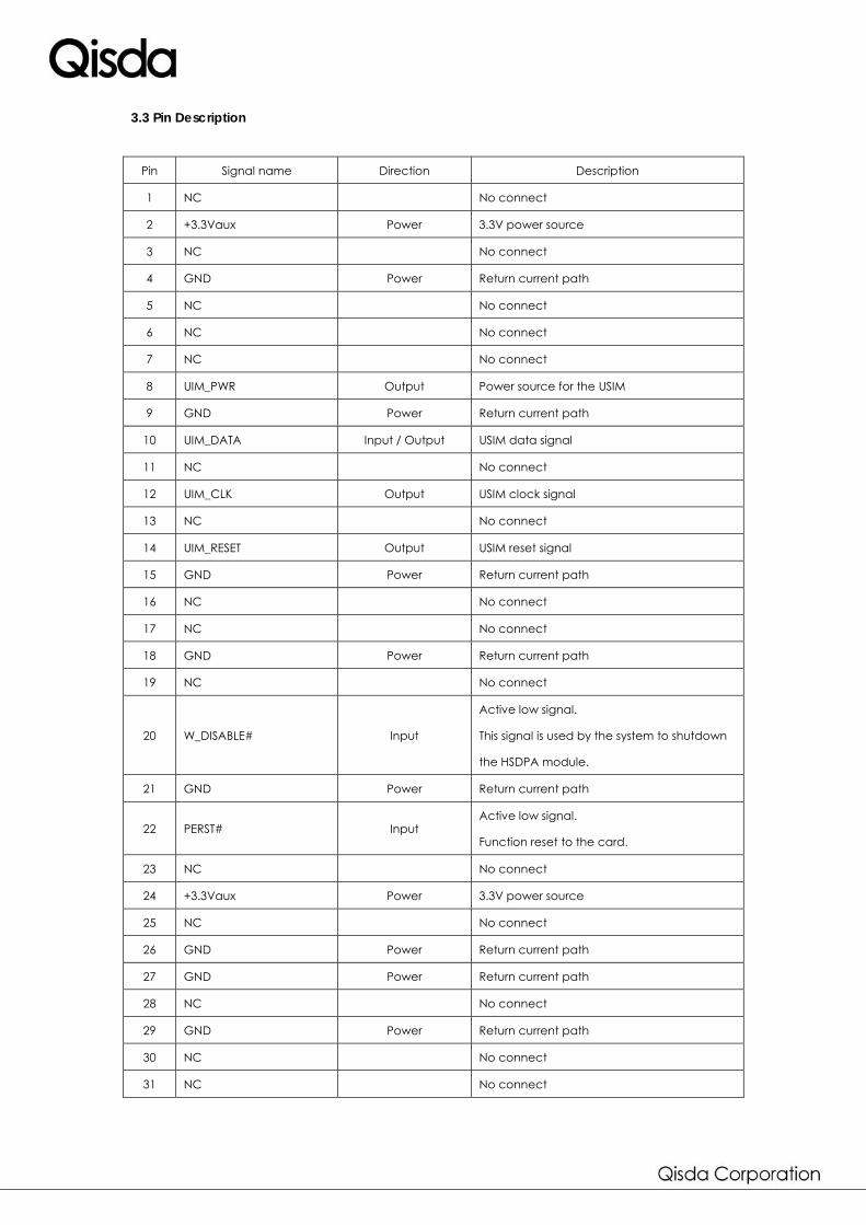
3.3 Pin Description
Pin Signal name Direction Description
1 NC No connect
2 +3.3Vaux Power 3.3V power source
3 NC No connect
4 GND Power Return current path
5 NC No connect
6 NC No connect
7 NC No connect
8 UIM_PWR Output Power source for the USIM
9 GND Power Return current path
10 UIM_DATA Input / Output USIM data signal
11 NC No connect
12 UIM_CLK Output USIM clock signal
13 NC No connect
14 UIM_RESET Output USIM reset signal
15 GND Power Return current path
16 NC No connect
17 NC No connect
18 GND Power Return current path
19 NC No connect
20 W_DISABLE# Input
Active low signal.
This signal is used by the system to shutdown
the HSDPA module.
21 GND Power Return current path
22 PERST# Input Active low signal.
Function reset to the card.
23 NC No connect
24 +3.3Vaux Power 3.3V power source
25 NC No connect
26 GND Power Return current path
27 GND Power Return current path
28 NC No connect
29 GND Power Return current path
30 NC No connect
31 NC No connect
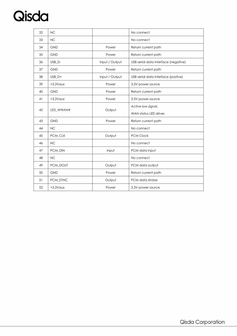
32 NC No connect
33 NC No connect
34 GND Power Return current path
35 GND Power Return current path
36 USB_D- Input / Output USB serial data interface (negative)
37 GND Power Return current path
38 USB_D+ Input / Output USB serial data interface (postive)
39 +3.3Vaux Power 3.3V power source
40 GND Power Return current path
41 +3.3Vaux Power 3.3V power source
42 LED_WWAN# Output Active low signal.
WAN status LED driver.
43 GND Power Return current path
44 NC No connect
45 PCM_CLK Output PCM Clock
46 NC No connect
47 PCM_DIN Input PCM data input
48 NC No connect
49 PCM_DOUT Output PCM data output
50 GND Power Return current path
51 PCM_SYNC Output PCM data strobe
52 +3.3Vaux Power 3.3V power source

3.4 Terminal Definition
Recommend antenna connect
Hirose Coaxial Connectors

System connector
The Qisda H20 PCIE Express interface compatibility Mini Card Electromechanical Specification
Revision 1.1.

3.5 Electrical Characteristics
DC characteristics
Pin Function/ Name Direction Parameter Min Typ Max Unit
1 NC
2 +3.3Vaux Power Power Supply Voltage 3.0 3.3 3.6 V
3 NC
4 GND Power Ground
5 NC
6 NC
7 NC
Supply Voltage 1.5 2.85 3.05 V 8 UIM_PWR Output
Current 150 mA
9 GND Power Ground
10 UIM_DATA Input / Output
11 NC
12 UIM_CLK Output
13 NC
14 UIM_RESET Output
15 GND Power Ground
16 NC
17 NC
18 GND Power Ground
19 NC
Logic High Input Voltage 0.7Vcc V 20 W_DISABLE# Input
Logic Low Input Voltage 0.3Vcc V
21 GND Power Ground
Logic High Input Voltage 0.65Vcc V 22 PERST# Input
Logic Low Input Voltage 0.35Vcc V
23 NC
24 +3.3Vaux Power Power Supply Voltage 3.0 3.3 3.6 V
25 NC
26 GND Power Ground
27 GND Power Ground
28 NC
29 GND Power Ground
30 NC
31 NC

32 NC
33 NC
34 GND Power Ground
35 GND Power Ground
36 USB_D- Input / Output Termination Voltage 3.3 V
37 GND Power Ground
38 USB_D+ Input / Output Termination Voltage 3.3 V
39 +3.3Vaux Power Power Supply Voltage 3.0 3.3 3.6 V
40 GND Power Ground
41 +3.3Vaux Power Power Supply Voltage 3.0 3.3 3.6 V
42 LED_WWAN# Output Driver current 10 mA
43 GND Power Ground
44 NC
45 PCM_CLK Output
46 NC
47 PCM_DIN Input
48 NC
49 PCM_DOUT Output
50 GND Power Ground
51 PCM_SYNC Output
52 +3.3Vaux Power Power Supply Voltage 3.0 3.3 3.6 V
◆ Power Supply:
Symbol Parameter Min Typ Max Unit
+3.3Vaux Power Supply Voltage 3.0 3.3 3.6 V
Isys System Current Consumption 2.5 A
※ The module draws more than 2.5A peak current while transmitting. Use wide
traces for power supply line and compliant with the PCB layout rule.
The current rating of component related with the power supply line must be
taken into consideration.

◆ Control Interface:
․W_DISABLE# :
Symbol Parameter Min Max Unit
VIH High Level Input Voltage 0.7Vcc V
VIL Low Level Input Voltage 0.3Vcc V
tpwron Power-on sequence interval 1.5 sec
High Level: Device Power on Low Level: Device Power off
※ W_DISABLE# must stay high at least tpwron to power on the Device.
․PERST# :
Symbol Parameter Min Max Unit
VIH High Level Input Voltage 0.65Vcc V
VIL Low Level Input Voltage 0.35Vcc V
Low Level: Reset H20
※ PERST# has internal pull-up resistor.
◆ USB Transceiver DC characteristics
The USB interface is powered from 3.3V power source.
Parameter Symbol Min Max Unit
Input Levels for Low/Full Speed
High VIH 2.0 V
Low VIL 0.8 V
Differential Input Sensitivity VDI 0.2 V
Input Levels for High Speed
High Speed Squelch Detection Threshold VHSSQ 100 150 mV
High Speed Disconnection Detection
Threshold
VHSDSC 100 150 mV
Output Levels for Low/Full Speed
Low VOL 0.0 0.3 V
High VOH 2.85 3.3 V

Output Levels for High Speed
High Speed Idle Level VHSOI -10.0 10.0 mV
High Speed Data Signaling High VHSOH 360 440 mV
High Speed Data Signaling Low VHSOL -10.0 10.0 mV
◆ USIM Interface
The USIM signals are defined on system connector to provide the interface between the
removable User Identity Module. USIM interface usually run off either 1.8V or 3.0V.
Pin Name Direction Description
8 UIM_PWR Output Power source for the USIM
10 UIM_DATA Input / Output USIM data signal
12 UIM_CLK Output USIM clock signal
14 UIM_RESET Output USIM reset signal
Parameter Symbol Min Max Unit
Logic High Input Voltage VIH 0.65‧VSIM VSIM +0.3 V
Logic Low Input Voltage VIL -0.3 0.35‧VSIM V
Input High Leakage Current IIH - 1 uA
Input Low Leakage Current IIL -1 - uA
Logic High Output Voltage VOH VSIM-0.45 VSIM V
Logic Low Output Voltage VOL 0 0.45 V
High-Level, Three-State Leakage
Current
IOZH - 1 uA
Low-Level, Three-State Leakage Current IOZL -1 - uA
Type I (8 Pins USIM socket)

Type II (6 Pins USIM socket)
◆ Current Driver Interface:
Parameter Min Typ Max Unit
LED_WWAN 10 mA
LED Application Circuit:
※ Recommend to reserve “Resistor” and “Capacitor” for improve RF wireless
performance.

◆ PCM Interface
The PCM interface runs at 2.048 MHz and uses 488 ns sync pulse (one 2.048-MHz clock tick),
and support linear (16 bits), u-law (8 bits) and a-law (8 bits) format.
The PCM_SYNC runs at 8 KHz with a 50% duty cycle.
PCM interface DC characteristics ( Vpcm=2.6V)
Parameter Symbol Min Max Unit
Logic High Input Voltage VIH 0.65‧Vpcm Vpcm +0.3 V
Logic Low Input Voltage VIL -0.3 0.35‧Vpcm V
Input High Leakage Current IIH - 1 uA
Input Low Leakage Current IIL -1 - uA
Logic High Output Voltage VOH Vpcm-0.45 Vpcm V
Logic Low Output Voltage VOL 0 0.45 V
High-Level, Three-State Leakage
Current
IOZH - 1 uA
Low-Level, Three-State Leakage Current IOZL -1 - uA
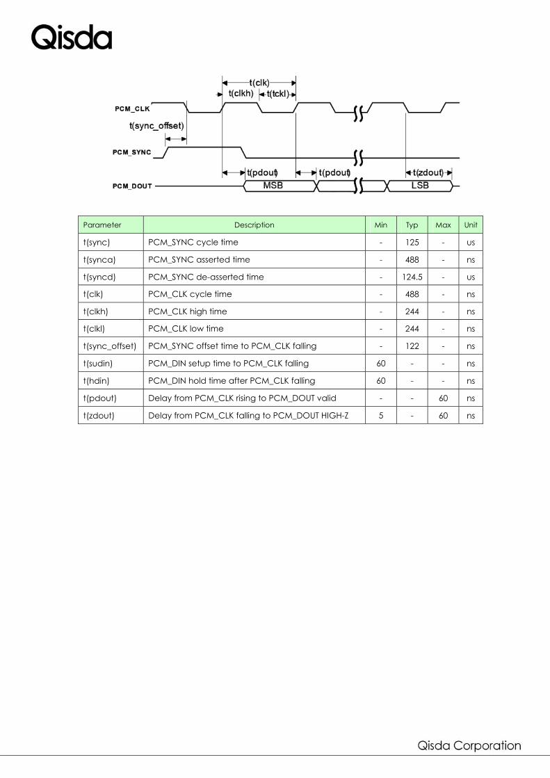
Parameter Description Min Typ Max Unit
t(sync) PCM_SYNC cycle time - 125 - us
t(synca) PCM_SYNC asserted time - 488 - ns
t(syncd) PCM_SYNC de-asserted time - 124.5 - us
t(clk) PCM_CLK cycle time - 488 - ns
t(clkh) PCM_CLK high time - 244 - ns
t(clkl) PCM_CLK low time - 244 - ns
t(sync_offset) PCM_SYNC offset time to PCM_CLK falling - 122 - ns
t(sudin) PCM_DIN setup time to PCM_CLK falling 60 - - ns
t(hdin) PCM_DIN hold time after PCM_CLK falling 60 - - ns
t(pdout) Delay from PCM_CLK rising to PCM_DOUT valid - - 60 ns
t(zdout) Delay from PCM_CLK falling to PCM_DOUT HIGH-Z 5 - 60 ns
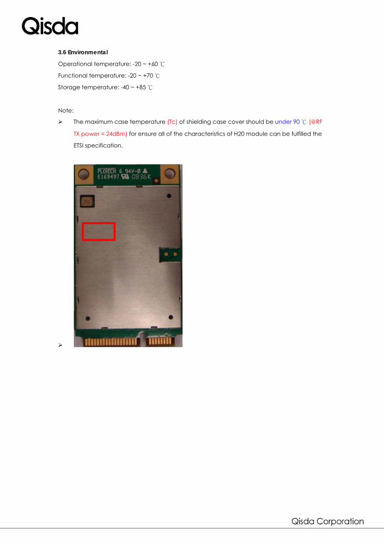
3.6 Environmental
Operational temperature: -20 ~ +60 ℃
Functional temperature: -20 ~ +70 ℃
Storage temperature: -40 ~ +85 ℃
Note:
The maximum case temperature (Tc) of shielding case cover should be under 90 ℃ (@RF
TX power = 24dBm) for ensure all of the characteristics of H20 module can be fulfilled the
ETSI specification.

3.7 Physical Package
Top View
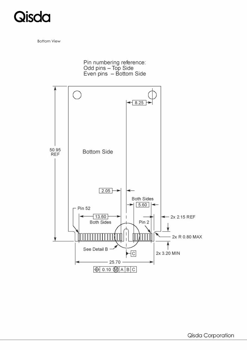
Bottom View
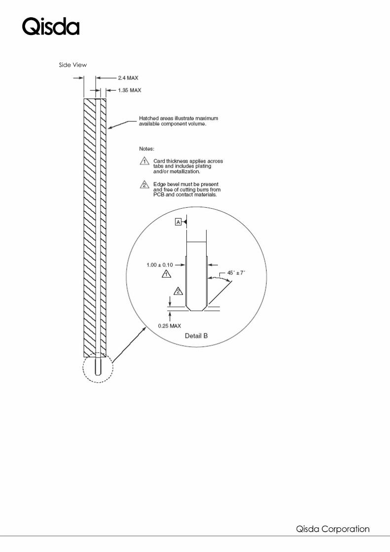
Side View
4. SOFTWARE CHARACTERISTICS
4.1 Introduction
H20 uses the cutting edge technique of Qualcomm 3.75G wireless communication. It is a
wireless data card product embedded in any host device which has mini-PCI Express
interface. The software platform is Qualcomm MSM7225. It uses USB interfaces to
communicate with PC/NB. The USB interfaces are composed of three parts “NDIS interface”,
“AT command Serial COM port” and “Qualcomm Diag COM port”. “Network app” use NDIS
interface to transmit Internet data between H20 device and Host device. PC tool (“SMS,
phone book and setting app”) can send the standard AT commands to drive H20 device by
“AT command Serial COM port”. “Qualcomm Diag COM port” interface is used for
Qualcomm and Qisda Factory tools. We can use this interface to get all device debug
messages and update the firmware of your H20 device.
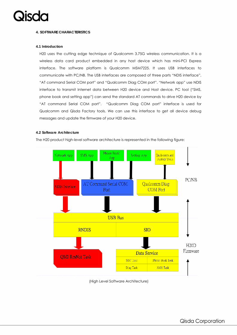
4.2 Software Architecture
The H20 product high-level software architecture is represented in the following figure:
(High Level Softw re Architecture)
a

4.2.1. The first layer is application layer.
(Application layer)
This layer contains network, SMS, phone book, device setting, Qualcomm and Qisda factory
tools. Qisda PC tool provides “network App, SMS App, phone book App and setting App”. User
can use this tool to surf the Internet and manage SMS messages, contact list, device settings.
“Qualcomm and Factory Tools” can support technician to get all debug message from H20
device.
4.2.2. The second layer is USB COM interface layer.
(USB COM interface layer)
H20 can support three different USB COM interfaces:
NDIS Interface – This interface is in charge of Internet data transmission between H20
and Host device.
AT command serial COM port- This a standard modem serial port. It can send/receive
the standard AT commands.
Qualcomm Diag COM port- This is Qualcomm proprietary interface, all
Debug/Download tools of Qualcomm and Qisda use this interface to transmit data.
4.2.3. The third layer is USB driver layer.
(USB driver layer)
This layer contains PC USB driver and H20 firmware USB driver. PC transmits data to H20 firmware
via this layer.
4.2.4. The fourth layer is RNDIS and SIO layer.
(RNDIS and SIO layer)
This layer works inside H20 firmware. RNDIS can process the NDIS data and command which USB

driver and QMI RmNet task transmit. SIO can process the AT and diag command which USB
driver and Data service transmit.
4.2.5. The fifth layer is task layer.
(Task layer)
This layer works inside H20 firmware. QMI RmNet Task is in charge of NDIS command for network
connection function. Data Service is in charge of processing all AT commands, including SIM,
Diag, Phone book and SMS task.
4.3 HSPA Modem Application
HSPA Modem Application is PC tool for end user to use. This tool contains four main functions-
network, SMS, phone book and setting application.

4.3.1. Network App uses NDIS interface to surf the Internet.
4.3.2. Phone Book App is in charge of the contact list, includes New, Edit, Export, Import
operations on your SIM card.

4.3.3. SMS App is in charge of SMS message receiving, sending, forward, reply, move, copy,
delete, new and backup operations.
4.3.4. Setting App includes some device settings about operator network setting and PIN
code setting.