h ig h a ltitu d e w e a th e r b a llo o n pr o je c...
TRANSCRIPT

Page 1
High Altitude Weather Balloon Project Patrick A. Costello
Menlo School
50 Valparaiso Street
Atherton, CA 94027
[email protected], [email protected]
April 14, 2008
ABSTRACT
The goal of the High Altitude Weather
Balloon Project is to send a balloon with
a payload to acquire weather data into
near space, approximately 33 km. The
project entailed designing both hardware
and software and modifying existing hardware. The project is still in progress
at this time.
Keywords
high altitude, weather balloon, ATV,
PIC microcontroller
1. MOTIVATION
The motivation for this project came
from the author’s interest after the Applied Science Research class did a
small-scale tethered balloon experiment
to 300 meters. Further motivation came
from J. Meehan’s balloon project on
http://vpizza.org/~jmeehan/balloon/,
which was found via http://www.hackaday.com.
2. HISTORY
Amateur high altitude weather balloons
are becoming increasingly popular with
amateur radio operators. Many people have used weather balloons to transmit
messages and to take aerial photography from the edge of space.
3. HARDWARE
The hardware schematics are available in Appendix A. The bill of materials for
the hardware design is available in
Appendix B. A picture of the flight
control board is in Appendix F.
3.1. Purchased Parts
The major portion of spending has gone
to purchasing equipment for radio
transmitting. Unfortunately, this is
completely necessary because without it there would be no data recovery and the
balloon would be lost. A complete list of
purchased parts is in Appendix D.
Copies of order forms are in Appendix
F.
3.2. Flight Controller
The flight controller is a 40-pin DIP
(Duel In-line package) dsPIC30F3014
from Microchip Technology Inc. Other
considered devices were the PIC16F887 and the PIC16F917. The dsPIC30F3014
was chosen because of its DIP
packaging, its UART (Universal
Asynchronous Receiver Transmitter)
Module, and its support for the
Microchip C30 Compiler.[1] The DIP packaging is important because it makes
integration into the circuit much easier because it can fit on normal prototyping
board without the need of an additional
socket. The double UART module with
alternate pins is important because 2 UART modules are needed, one for GPS
connection (see GPS) and one for connection to the radio and PC (see
Radio). The Microchip C30 compiler allowed the dsPIC30F3014 to be
programmed in the C programming language. Photos of the hardware are in
Appendix F.

Page 2
3.2.1 UART The UART configuration requires
several initialization registers to be set. An important set up is the baud rate
generator in the special function register
UxBRG. Equation 1 contains the
equation used to calculate the UxBRG
special function register. Other initialization needs are shown in the
code in Appendix E. 3.2.2 Crystal
The crystal oscillator used is a 9.8304
MHz crystal. 9.8304 MHz is optimal
because when used in baud rate calculations for typical baud rate values,
it generates clean numbers with no error
for the baud rate generator. Typical
values are 1200 baud and 9600 baud. When the UxBRG is calculated, there
will normally be a slight error, for example with a 4 MHz clock frequency
the error is 0.16 percent. [2] This error can offset UART data transmission,
which could lead to jumbled data. Using
the 9.8304 MHz crystal, this error
becomes 0 percent. 3.3. GPS
The GPS module chosen was the Jupiter TU30-D140 OEM (Original Equipment
Manufacturer) module from Rockwell International. The Jupiter module was
chosen because of its low cost and lightweight. It has no unnecessary
buttons, screens, etc. that are included on normal commercial GPS devices. It has
a UART module that outputs at 4800 baud on TTL levels. This is perfect for
integration with the PIC UART. The GPS outputs data that is based on
NMEA-0183 mode protocols.[3] The
antenna used for the GPS is an active
antenna, which increases the signal strength by a gain of 26dB.[4]
3.4. Memory
The memory chips chosen were 16-
megabit DataFlash chips (AT45DB161D) made by Atmel. This
chip is ideal because of its SPI (Serial Peripheral Interface) that can interface
directly with the PIC. Unfortunately, the
chip can only be written in 512 page
increments, so each page will contain a significant amount of filler bits. Writing
to the flash is very easy and only
requires a single opcode.
3.4.1 MicroSD Option
The other memory device that was
considered was a microSD card [6], similar to those found in digital cameras.
The microSD card would allow for more
data, an elegant FAT32 file system, and
easy transfer of data to the PC. However,
implementing the FAT32 file system and
using the SD card would be difficult to implement and would add unnecessary
complexity to saving data.
3.5. Sensors
The sensors on board the payload are two temperature sensors, one pressure
sensor, and one accelerometer. Data
sheets for the sensors are in Appendix J.
3.5.1 Temperature Sensor
The two temperature sensors used are the LM335 from National
Semiconductor and the LM135 from National Semiconductor. [8] The LM335
has an operating range of -40˚C to 100˚C while the LM135 has an operating range
of -55˚C to 150˚C. The LM135 is
necessary for the external sensor because
!
UxBRG =FCY
16" Baud Rate#1
Equation 1: Equation for
determining the UART baud rate
generator special function register
value. [2] In this equation, FCY is the processor clock frequency, and Baud
Rate is the desired baud rate. ‘x’ denotes the UART channel.

Page 3
the temperature between 0 meters and 30,000 meters can reach temperatures as
far as -65˚C. [9] 3.5.2 Pressure Sensor
The pressure sensor used is the
MPXM212D/A from Freescale
Semiconductor. [10] The pressure sensor is optimized for a 10-volt power supply,
so additional amplification was necessary for proper data
acquisition.[11] 3.5.3 Signal Amplification
Both pressure and temperature data was amplified using the LMC6042 Duel Op
Amp (Operational Amplifier). [12]
3.5.4 Accelerometer
The accelerometer selected was the MMA1270 from Freescale
Semiconductor. [13] The MMA1270 is a
single-axis accelerometer, allowing the
measurement of z-axis acceleration. The
z-axis is of most interest because side-to-
side acceleration should be very minimal.
3.6. Radio
The radio system will transmit data
using packet radio. ITU (International
Telecommunications Union) codes
requires using radio bands specific to packet radio. Most of these bands
require at least a technician class
amateur radio license from the FCC. The most used packet radio frequencies are
in the 2 meter band, between 144.90 and 145.10 MHz. Packet radio in this range
operates on odd frequencies every 20
kHz. This means the operating
frequencies are 144.91 MHz, 144.93 MHz, … 145.09 MHz. [14]
3.6.2 Balloon Radio
The radio finally chosen for transmission
from the weather balloon was the Kenwood TH-D7A. This radio is
preferred because it has a built-in terminal node controller (TNC). The
TNC is what converts the data signals to
radio signals (and vice-versa).
3.6.3 Recovery Vehicle Radio
The radio chosen for the recovery
vehicle was the TH-D7A’s mobile
counterpart, the Kenwood TM-D710A.
This radio is built just like the TH-D7A,
but it runs off the car battery supply, and
has higher sensitivity, allowing it to pick up and transmit better signal. The TM-
D710A also has a built-in TNC with a
serial port connection.
3.7. Camera
The payload will be equipped with 5
cameras, one on each side and one pointed directly down. The cameras used
are Digital Single-Use Cameras from
GPS TEXT, TIME, LAT, N or S, LONG, W or E, SIGNAL, SATS, MAG, ELEV, M, +/-, M, , NUM, PRESS, ACCEL, INT TEMP, EXT TEMP, CHECKSUM
$GPGGA,140546,4049.9762,N,11920.9620,W,1,10,0.82,1269.1,M,-20.8,M,,0355,AB9,A87,461,4F8,*121A
$GPGGA,140547,4049.9762,N,11920.9620,W,1,10,0.82,1269.1,M,-20.8,M,,0356,ACA,A82,021,007,*11FD
$GPGGA,140548,4049.9762,N,11920.9620,W,1,10,0.82,1269.1,M,-20.8,M,,0357,A8A,A7E,462,4FB,*1234
$GPGGA,140549,4049.9762,N,11920.9620,W,1,10,0.82,1269.1,M,-20.8,M,,0358,AB6,A81,45F,4F8,*122B
Figure 1: Data transmitted from flight controller. The data transmitted from the
flight controller includes GPS, pressure, acceleration, internal temperature, external temperature, sample number, and a checksum. All values—besides GPS—are hex
values. Following the GPS data, there are four comma separated values, followed by a checksum. The first number is the packet number. The second number is the pressure,
the third acceleration, the fourth internal temperature, and the fifth is external
temperature.

Page 4
Longs Photo. The cameras are made by Pure Digital Technologies, and are
model 400. These digital cameras have a photo limit of 25 pictures, and must be
returned to the store for processing.
However, it is possible to unlock the
firmware [15], allowing the photos to be processed using a USB connection and
allows the cameras to be used more than once. The cameras were unlocked and
wired to allow for power-on and shutter control to be controlled by the flight
controller. The eyepiece, flash, and flash capacitor were removed from the flash
because they are not needed. Photos of
the camera are in Appendix F.
3.8. Cut-down Device
The cut down device was designed as a
U shaped metal piece with a bolt through
the top of the U (making it into a ring).
This bolt would be attached to a motor,
and then when the cut-down call is
made, the PIC microcontroller will supply power to the motor, removing the
bolt and allowing the balloon to float
freely away from the payload. See
Appendix C for the cut-down device
sketch design.
3.8.1 Problems with Cut-down
Device
The cut-down device was never
implemented due to the problem of
supplying power to the cut-down. A wire may have interfered with the parachute,
causing the payload to descend too
quickly. An option in implementing the
cut-down device would be providing power and the cut-down signal remotely,
but this would require a separate power source and implementation of a short-
range wireless device. This option was not explored due to lack of time.
3.9. Landing Device
The landing device consists of a piezo
beeper that begins beeping after 90
minutes. This allows the device to be
found if it lands out of line-of-sight. The beeper has a power-off switch, allowing
the finder to turn it off. 4. SOFTWARE
The software was programmed in the C
programming language using
Microchip’s MPLAB integrated development environment. The code was
compiled using a student edition of Microchip’s C30 Compiler. For the
complete code, see Appendix E. 4.1. Program modes
The flight controller has 3 different program modes, determined by jumper
configurations in hardware. The three
modes are: Acquire Data, Erase Flash,
and Transmit to PC. 4.2. Acquire Data
The acquire data program mode handles
all acquisition of hardware and in-flight
operations. Operation is controlled by a
combination of interrupts and hard-
coded commands. The operation is as follows:
1.Initialize UART1 for GPS receiving.
2.Initialize UART2 for radio interaction.
3.Wait for GPS packet to be read.
4.Read A/D values.
5.Add a checksum. 6.Write packet to flash and radio.
7.Repeat steps 3-6.
4.3. Erase Flash
The erase flash program fully erases the flash, which must be done one page at a
time. This will be done pre-launch to
ensure maximum acquisition of data.
4.4. Transmit to PC
The transmit-to-PC program transmits
all the data on the flash to the PC. This program also parses the data to eliminate
all meaningless data. This increases the speed at which the flash can be read,
because reading the entire flash over the UART would take approximately 30
minutes.

Page 5
5. DATA
The data syntax transmitted from the
flight controller is very similar to that of the NMEA protocol data. A sample of
the data can be seen in Error! Reference
source not found. The data values are
hex values, and each sample is separated by a carriage return.
5.1. Sample Number The sample number counts up by one
every time a sample is sent (every second). This is useful because it resets
when the chip resets, so if the chip resets during flight, which will interrupt data
communication, the packet number will
be able to confirm a flight controller
reset. If the flight controller stops receiving GPS data, the sample number
will allow the flight controller to keep
track of time and collect data at a slower
rate of one sample per 2 seconds.
6. PAYLOAD AND FLIGHT
STRING 6.1. Payload
The payload was constructed from a
insulated cooler from Target. The top
half of the payload was dedicated to the
flight controller and radio, and the
bottom half was used for the cameras. The camera was placed in the bottom
because they were less important to the
recovery of the balloon, and in the result
of a hard landing would be the first to go.
6.2. Flight String
The flight string was designed to prevent
the balloon from becoming entangled in the parachute, forcing the payload to
descent too rapidly. The flight string was assembled, top to bottom, as follows:
1. Balloon 2. 4 feet string
3. Small parachute (dangling) 4. 12 feet string
5. large parachute (in-line)
6. payload
The purpose of the small parachute is to hold the balloon shards far above the
main parachute. 6.3. GPS Antenna
The GPS antenna, which was initially
designed to go directly on top of the
payload box, had to be placed 6 feet to the side of the payload due to radio
interference from the radio antenna. At first, the GPS antenna wire was coiled
around the wood post holding it away from the payload, but it would not
receive GPS data in that position. The only position it successfully received
GPS data in was when the antenna wire
was dangling. While the radio was the
main factor in interfering with the GPS signal, the antenna may also have been
broken from transit.
7. RESULTS
All raw data is available in the excel
spreadsheet “Raw Data.xls”, which is
available from the author of this paper or on http://www.pcostello.com.
7.1. Pressure
The pressure data follows the expected
trend of moving inversely to the altitude,
as shown in Figure 2. However, as show
in Figure 3, there is some error. This may be a result of the accuracy of the
sensor, or the fact that it was placed
inside the payload rather than on the
outside, effecting both the pressure and the temperature of the air around the
sensor.

Page 6
Figure 2: Pressure versus Time. This
graph shows pressure data acquired over
the length of the flight (red). Altitude data is included on the right y-axis as a
reference (purple).
Figure 3: Calculated altitude from
pressure compared with altitude
acquired from GPS versus time. The
blue line represents the calculated altitude from pressure and external
temperature in Equation 2. The purple
line represents the altitude data acquired
from GPS readings.
!
h =
kT ln(Ph
P0)
mg
Equation 2: Altitude equation based
on the barometric equation. Variables
are Ph and T. This equation is derived in Appendix G.
7.2. Temperature 7.2.1 External Temperature
The external temperature reached lows of -40.3 ºC. This is slightly warmer than
the expected minimum of -60 ºC. A
possible reason for this temperature
difference could be the particular area in the atmosphere, or close proximity to the
payload could have led to higher temperatures due to radiating heat from
the internal electronics and heating devices.
Figure 4: External Temperature (ºC)
versus time. The external temperature data in orange is ploted against flight
time, with a purple altitude for reference.
As seen in Figure 4, the external
temperature decrease with an increase in
altitude until it reaches approximately
40ºC. The reason for this is that at approximately that altitude the
troposphere ends and the stratosphere
begins. In the stratosphere (also know as
the ozone layer), radiation from the sun cause O3 to break into O2 and O,
releasing heat in the process, as shown in
Diagram 1.

Page 7
Diagram 1: Temperature versus
height in the troposphere and
stratosphere. [16]
Figure 5 shows altitude versus
temperature in the same format as
Diagram 1 for a better comparison.
Figure 5: Altitude versus
Temperature. The purple line
represents the changing altitude versus the external temeprature. The line has
multiple data for each temperature point due to data being acquired on both the
ascent and the descent.
7.2.2 Internal Temperature
The internal temperature was kept in a
relatively safe range between
approximately -1ºC and 20ºC. The internal temperature is very important
because all of the electrical components have a temperature operating range. If
the temperature inside the payload exceeded this range (either by being too
hot or too cold), the electronics could
stop working causing a loss in data acquisition or transmission, causing the
payload to be lost.
Figure 6: Internal temperature versus
time. The internal temperature (green) is plotted against flight time with the
external temperature (orange) and
altitude (purple) as references.
The internal temperature, as shown in Figure 6, had a small range in
comparison to the external temperature.
Reasons for this include heat warmers
placed in the balloon and heat generated
by the electronics.
7.3. Acceleration The acceleration data, as shown in
Figure 7, is much less stable and linear
than the temperature and pressure data,
and as a result is more difficult to
interpret. Areas of note are the balloon
burst and the landing. A significant change in the acceleration data is shown
at these two points.
Figure 7: Acceleration versus time.
The acceleration (blue), measured in G-

Page 8
forces versus time with altitude (purple) as a reference. The acceleration data is
zeroed around -1g, the gravitational force. Acceleration in the negative
direction indicates acceleration towards
the ground.
7.4. Photos from the Payload
Cameras
Photos from the payload cameras are available in Appendix H.
8. LAUNCH AND FLIGHT PATH The launch took place at
40°49'58.23"N, 119°20'57.75"W at 14:21:28 Z on May 4, 2008. Flight lasted
1 hour and 16 minutes, touching down at
15:37:31 Z on May 4, 2008 at
40°58'36.84"N, 119° 5'54.32"W. The straight-line path from the launch point
to the landing point was 26.5 km. The
approximate over-land distance traveled
by the balloon was 36.6 km.
Figure 8: Balloon flight path via
Google Earth. The blue represents the flight path of the balloon.
The flight path and predicted flight path are available as “Flight Path.gpx” and
“Predicted Flight Path.kml”,
respectively. Predicting the flight path
also used an ascent rate calculator,
provided as “Ascent Rate
Calculator.xml”.
9. CONCLUSION
This project brought together the need
for both hardware and software design. Building, coding, and debugging on a
large project is incredibly time consuming and at times painful. Finally
launching, and the recovering, was very rewarding.
9.1 Furthering Research
A major thing that needs to be changed
is the type of balloon. The balloon used was from Scientific Online, but there are
much better balloons available from Kaymont Consolidated. Another major
change may be GPS. The GPS antenna definitely should be replaced with a
better one, or at least a new one. However replacing the GPS module may
also be a good idea. The current GPS
module seems to be falling apart, and it
may make sense to get a new, not discontinued GPS. Another change
would be to add additional sensors.
There were many sensors that would be
interesting additions, such as CO 2,
oxygen content, etc. Another interesting
addition would be an ATV board and a video camera in order to stream live
video.
10. ACKNOLEDGEMENTS
This project could never have been
completed without help from Peter
Costello. He acted as a mentor, a guide, and a source of knowledge. Thank you.
11. REFERENCES
[1] “dsPIC30F3014, dsPIC30F4013
Data Sheet.” Microchip Technology Inc.
[2] “dsPIC30F Family Reference
Manual.” Microchip Technology Inc.
[3] “Rockwell Jupiter GPS Module.” Available from:
http://www.gpskit.nl/gps-readme.html. Accessed on: April 14,
2008. [4] “Antenna GPS 3V Magnetic Mount
MCX.” Sparkfun Electronics. Available from:
http://www.sparkfun.com/commerce/

Page 9
product_info.php?products_id=8254. Accessed on: April 14, 2008.
[5] “AT45DB161D.” Atmel Corporation.
[6] “SD Specifications: Part 1. Physical
Layer: Simplified Specification.”
Version 2.00, September 25, 2006. SD Group.
[7] “Microsoft extensible Firmware Initiative FAT32 File System
Specification.” Version 1.03, December 6, 2000. Microsoft Corp.
[8] “LM135/LM235/LM335, LM135A/LM235A/LM335A
Precision Temperature Sensors.”
November 2000. National
Semiconductor. [9] “Radiosonde Data.” University of
Wyoming. Available from:
http://weather.uwyo.edu/cgi-
bin/sounding?region=naconf&TYPE
=TEXT%3ALIST&YEAR=2008&
MONTH=04&FROM=0312&TO=0312&STNM=72489. Accessed on:
April 14, 2008.
[10] “100 kPa On-Chip Temperature
Compensated & Calibrated Silicon
Pressure Sensors.” Rev 4, September 2005. Freescale Semiconductor.
[11] Schultz, Warren. “Amplifiers for Semiconductor Pressure Sensors.”
Rev 3, May 2005. Freescale
Semiconductor.
[12] “LMC6042 CMOS Dual Micropower Operational Amplifier.”
August 2000. National Semiconductor.
[13] “Low G Micromachined Accelerometer.” Rev 4, September
2005. Freescale Semiconductor. [14] “ARRLWeb: ARRL Band
Plans.” American Radio Relay
League. December 14, 2006.
Available from: http://www.arrl.org/FandES/field/reg
ulations/bandplan.html. Accessed on:
15 April 2008.
[15] Camerahacking.com. Available
from:
“http://camerahacks.10.forumer.com/” Accessed on: April 20, 2008.
[16] “The Stratosphere.” Available from:
http://apollo.lsc.vsc.edu/classes/met130/
notes/chapter1/vert_temp_strat_o3.html.
Accessed on: May 15, 2008.

Appendix A: Hardware Schematic
Page 10

Appendix A: Hardware Schematic
Page 11

Appendix A: Hardware Schematic
Page 12

Part Number Value Digikey Part #B1 6V
C1 470uF
C2 470uF
C3 .1uF
C4 .1uF
C5 .1uF
C6 .1uF
C7 .1uF
C8 .1uF
C9 .1uF
C10 .1uF
C11 .1uF
C12 .1uF
C13 .1uF
C14 .1uF
C15 22pF PCC1973CT-ND
C16 22pF PCC1973CT-ND
C17 .1uF
C18 .1uF
C19 .1uF
C20 .1uF
C21 .1uF
C22 .01uf
C23 0.001uF
C24 1000pF
C25 .01uF
C26 1000pF
C27 220uF
D1
J1
J2
J3
J4
JP3
JP4
Q1
Q2
Q3
R1 15
R2 15
R3 100K
R4 100K
R5 1k
R6 16.9K
R7 1.78K
R8 23.2K
R9 383K
R10 105
R11 44.2K
R12 200
R13 3K
R14 10.2K
Appendix B: Bill of Materials
Page 13

R15 24.9K
R16 6.81K
R17 6.55K
R18 3K
R19 10.2K
R20 24.9K
R21 4.7K
R22 15
R23 15
R24 3.9K
R25 4.7K
R26 4.7K
R27 4.7K
R28 1K
SW1
U1 dsPIC30f3014 DSPIC30F301430/P-ND
U2 LM7905 296-8157-5-ND
U3 AT45DB161D AT45DB151D-SU-ND
U4 AT45DB161D AT45DB151D-SU-ND
U5 ST202E 497-3009-5-ND
U6 MMA1270 MMA1270EG-ND
U7 MPXM2102A MPXM2102A-ND
U8 LM335 LM335ZNS-ND
U9 LM135 LM135SAH-ND
U10 LMC6042 LMC6042AIN-ND
U11 LMC6042 LMC6042AIN-ND
U12 LM709033 497-1510-5-ND
U13 BEEPER 668-1056-ND
X1 9.8304 MHz X1097-ND
Appendix B: Bill of Materials
Page 14

Appendix C: Cutdown Device
Page 15

Item Type Item Supplier Part Number Date Ordered Price Quanity Total Purchased Purchase Type Total Cost
GPS Rockwell Jupiter eBay January 21, 2008 $31.99 $31.99 Expense $31.99
Book Ham Radio for DummiesAmazon January 23, 2008 $14.95 $14.95 No Purchase
Book Ham Radio: Simplified Amazon January 23, 2008 $8.95 $8.95 No Purchase
Camera 5.0M Pixel Webcam eBay January 25, 2008 $11.88 $11.88 No Purchase
GPS GPS Passive Antenna eBay January 25, 2008 $8.94 $8.94 No Purchase
Sensor Temperature Sensor Digikey LM335ZNS-ND January 27, 2008 $1.21 5 $6.05 Expense $1.21
Sensor Accelerometer Digikey MMA7360LT-ND January 27, 2008 $6.10 1 $6.10 No Purchase
Sensor Pressure Sensor Digikey MPXM2102A-ND January 27, 2008 $9.55 2 $19.10 Expense $9.55
Memory Kingston 1GB MicroSD CardAmazon February 14, 2008 $9.15 2 $18.30 No Purchase
Connector Flash Connector Digikey 3M5607CT-ND February 18, 2008 $1.16 $1.16 No Purchase
IC IC RS232 Transceiver Digikey 497-2052-1-ND February 18, 2008 $1.61 2 $3.22 No Purchase
Connector Flash Connector Digikey 670-1528-1-ND February 18, 2008 $1.91 $1.91 No Purchase
Memory IC 16MB Flash Digikey AT45DB161D-CNU-ND February 18, 2008 $2.37 2 $4.74 Expense $4.74
Memory IC 64MB Flash Digikey AT45DB642D-CNU-ND February 18, 2008 $6.99 2 $13.98 No Purchase
Connector microSD Breakout BoardSparkfun Electronics BOB-00544 February 18, 2008 $14.95 $14.95 No Purchase
Connector Flash Connector Digikey CCM01-6202LFT February 18, 2008 $1.55 $1.55 No Purchase
Connector Flash Connector Digikey HR1929CT-ND February 18, 2008 $3.00 $3.00 No Purchase
Connector Flash Connector Digikey HR1938CT-ND February 18, 2008 $2.99 $2.99 No Purchase
Connector Flash Connector Digikey HR1940CT-ND February 18, 2008 $2.38 $2.38 No Purchase
Connector Flash Connector Digikey HR846CT-ND February 18, 2008 $4.09 $4.09 No Purchase
Sensor IC Temp Sensor Digikey MCP9803-M/SN-ND February 18, 2008 $1.58 4 $6.32 No Purchase
Connector Flash Connector Digikey WM19079CT-ND February 18, 2008 $3.12 $3.12 No Purchase
Connector Flash Connector Digikey WM19081CT-ND February 18, 2008 $4.61 $4.61 No Purchase
Crystal 4.9152 MHz Crystal Digikey X1049-ND February 18, 2008 $0.58 2 $1.16 No Purchase
Crystal 7.3728 MHz Crystal Digikey X1084-ND February 18, 2008 $0.75 2 $1.50 No Purchase
Crystal 9.8394 MHz Crystal Digikey X1097-ND February 18, 2008 $0.58 2 $1.16 No Purchase
Crystal 14.7456 MHz Crystal Digikey X1102-ND February 18, 2008 $0.58 2 $1.16 No Purchase
Crystal 19.6608 MHz Crystal Digikey X1108-ND February 18, 2008 $0.58 2 $1.16 No Purchase
Crystal 3.6864 MHz Crystal Digikey X402-ND February 18, 2008 $0.58 2 $1.16 No Purchase
GPS GPS Active Antenna Sparkfun Electronics GPS-08254 February 28, 2008 $12.95 $12.95 Expense $12.95
IC IC Reg 5V Digikey 296-8157-5-ND March 4, 2008 $5.40 4 $21.60 Expense $5.40
IC IC Reg 3.3V Digikey 497-1510-5-ND March 4, 2008 $2.55 4 $10.20 Expense $2.55
IC IC RS232 Digikey 497-3009-5-ND March 18, 2008 $1.95 2 $3.90 Expense $1.95
Connector Header .100 Digikey 929550-01-36-ND March 18, 2008 $3.96 1 $3.96 Expense $3.96
Appendix D: Parts Purchased
Page 16

Connector 40 pin DIP Socket Digikey A411-ND March 18, 2008 $1.93 2 $3.86 No Purchase
Connector 18PIn SOIC Socket Digikey A736-ND March 18, 2008 $5.87 2 $11.74 Expense $11.74
Memory IC 16MB Flash 2.5V Digikey AT45DB161D-SU-2.5-ND March 18, 2008 $2.37 4 $9.48 No Purchase
IC dsPIC30F3014 Digikey DSPIC30F301430/P-ND March 18, 2008 $8.85 2 $17.70 Expense $8.85
IC OP AMP Dual Digikey LMC6042AIN-ND March 18, 2008 $2.53 4 $10.12 Expense $5.06
Sensor Accelerometer Digikey MMA1270EG-ND March 18, 2008 $11.51 $11.51 Expense $11.51
IC Charge Pump Digikey TC962CPA-ND March 18, 2008 $2.53 2 $5.06 No Purchase
Radio 2M Mobile Ant Ham Radio Outlet AX-75 April 5, 2008 $49.95 2 $99.90 Capital $99.90
Radio 16.5 ft Coax Ham Radio Outlet CK-3M5 April 5, 2008 $34.95 $34.95 Capital $34.95
Radio 18 inch SMA to SO-239Ham Radio Outlet HS-05 April 5, 2008 $11.95 $11.95 Capital $11.95
Radio PC to THD7A Cable Ham Radio Outlet PG-4W April 5, 2008 $45.95 $45.95 Capital $45.95
Radio Luggage Rack Mount Ham Radio Outlet RS-560C April 5, 2008 $29.95 $29.95 Capital $29.95
Radio Handheld Radio Ham Radio Outlet TH-D7A(G) April 5, 2008 $329.95 $329.95 Capital $329.95
Radio Mobile Radio Ham Radio Outlet TM-D710A April 5, 2008 $589.95 $589.95 Capital $589.95
Connector DB9 Backshell Digikey 609-1424-ND April 7, 2008 $1.89 3 $5.67 No Purchase
Connector DB9 Male Soldercup Digikey 609-1524-ND April 7, 2008 $1.53 2 $3.06 No Purchase
Connector DB8 Female Soldercup Digikey 609-1525-ND April 7, 2008 $1.56 2 $3.12 Expense $3.12
IC Piezo Beeper Digikey 668-1056-ND April 7, 2008 $8.66 1 $8.66 Expense $8.66
Connector 18PIn SOIC Socket Digikey A750-ND April 7, 2008 $6.95 3 $20.85 Expense $13.90
Connector 2.5mm 6' Cable Digikey CP-2204-ND April 7, 2008 $2.49 2 $4.98 No Purchase
Connector 2.5mm Connector Digikey CP-2501SP-ND April 7, 2008 $0.96 2 $1.92 No Purchase
Sensor IC Temp Sensor Digikey LM135AH-ND April 7, 2008 $16.59 $16.59 Expense $16.59
Crystal 9.8304 MHz Crystal Digikey X1097-ND April 7, 2008 $0.58 4 $2.32 Capital $0.58
Parachute SkyAngle Swivel Omega Rocketry April 25, 2008 $3.75 2 $7.50 Capital $7.50
Parachute SkyAngle Classic II 44 Omega Rocketry April 25, 2008 $66.00 $66.00 Capital $66.00
Parachute SkyAngle Streamer 3" Omega Rocketry April 25, 2008 $10.00 $10.00 Capital $10.00
Connector Conn Power Plug Digikey CP3-1003-ND April 25, 2008 $0.93 2 $1.86 Capital $0.93
Connector Holder AA 4Cell Digikey 2478K-ND April 25, 2008 $1.43 4 $5.72 Capital $2.86
Connector Holder AA w/ 9V snap Digikey 2476K-ND April 25, 2008 $1.43 4 $5.72 Capital $1.43
Connector Cord DC plug w/ fuse Digikey ZA5073-2.5-ND April 25, 2008 $5.47 $5.47 No Purchase
IC CAP .33F Gold Digikey P11065-ND April 25, 2008 $1.85 $1.85 Expense $1.85
Battery Lithium Battery Digikey N602-ND April 25, 2008 $3.33 30 $99.90 Expense $99.90
Connector Strap Battery 9V Digikey 2243K-ND April 25, 2008 $0.89 2 $1.78 No Purchase
Parachute SkyAngle Classic 20 Omega Rocketry April 30, 2008 $20.00 $20.00 Capital $20.00
Appendix D: Parts Purchased
Page 17

Total By Item Type Total $1,759.23
IC Total $82.31 Total with Tax $1,904.37
Connector Total $119.47
Memory Total $46.50 MENLO SCHOOL
Crystal Total $9.62 Capital Purchases $1,251.90
Sensor Total $65.67 Project Expenses $255.48
GPS Total $53.88 Sales Tax $124.36
Camera Total $11.88 TOTAL COSTS $1,631.74
Book Total $23.90
Radio Total $1,142.60 PATRICK COSTELLO
Paracute Total $103.50 Surplus Inventory $251.85
Battery Total $99.90 Sales Tax $20.78
Total $1,555.83 Shipping No Receipts
Appendix D: Parts Purchased
Page 18

/*******************************************
*
* High Altitude Weather Balloon Project
*
* Author: Patrick Costello
* Date: May 2, 2008
*
* This program was designed for use the Microchip
* C30 Compiler. It was developed specifically for
* the dsPIC30F3014.
*
**********************************************/
#include <p30f3014.h>
#include "WeatherBalloo.h"
/* Interrupt macros */
//#define _ISR __attribute__((interrupt))
//#define _ISRFAST __attribute__((interrupt, shadow))
#define _ISRFASTx __attribute__((interrupt, shadow, no_auto_psv))
/********************************************
* Config Bits *
********************************************/
// _FOSC(XT); // 9.8304MHz Crystal
_FOSC( CSW_FSCM_OFF & HS ) // 9.8304MHz
// _FOSC( CSW_FSCM_OFF & FRC & HS ) // 8MHz
// Enable Watchdog to 6sec
_FWDT( WDT_ON & WDTPSA_512 & WDTPSB_6 )
// Enable Brown-out Reset at 4.5 Volts and initialize the Power-up
// timer to 64 milliseconds and configure the use of the MCLR pin for
I/O.
_FBORPOR( PBOR_ON & BORV_45 & PWRT_64 & MCLR_DIS )
/********************************************
* Variables *
********************************************/
// 3 programs. Controlled by switches.
int programMode;
#define EchoGPS 0
#define TransmitToPC 1
#define AcquireData 2
#define EraseFlash 3
#define LED PORTDbits.RD2
#define LEDON 0
#define LEDOFF 1
Appendix E: Software Code
Page 19

#define CAMERA_ON PORTDbits.RD8
#define CAMERA_SHOOT PORTDbits.RD9
#define ALARM PORTDbits.RD3
#define CUTDOWN PORTAbits.RA11
// Note: Back-to-Back "RF0=1; RF1=1" fails. Use "PORTF |= 3".
#define EnableFlash0 PORTFbits.RF0=0;
#define EnableFlash1 PORTFbits.RF1=0;
#define DisableFlash PORTF |= 0x3;
#define TRUE 1
#define FALSE 0
// Variable managed by RS232 interrupts
#define BUFLEN 256 // AX.25 allows upto 256
bytes per packet
#define BUFMASK 0xFF
#define BUF0 0 // 1st half of 'buf'
#define BUF1 BUFLEN // 2nd half of 'buf'
#define RESERVED_BUFLEN 40 // #Reserved char for
";N0123P012A012T012T012*0123\n"
unsigned char buf[BUFLEN*2];
long seconds=0; // Number of seconds since
RESET
int skipPacket=FALSE; // Skip current packet?
int validLine=FALSE; // Save current GPS line?
int gotPacket=FALSE; // 0=Idle, 1=executing
ProcessPacket()
int uart2Active=FALSE; // 0=Idle, 1=Uart2 Active
int dollarIndex=BUF0; // Last '$' in 'buf'
int writeIndex=BUF0; // Current write index into 'buf'
int packetEnd; // Index for end of packet in
'buf'.
int uart2Index; // Read index in 'buf' for
output to radio
unsigned int txThrottle=0; // Limit radio to 1packet in 4 sec
to extend battery life
#define TxRate 4 // Radio transmit every 4 sec
// Variables managed by flash interface
int flashChip=0; // Chip 0 or Chip 1. If 2+, then
flash is full
int flashPage=0; // Page = 0..4095
int flashByte=0; // Byte = 0..527
Appendix E: Software Code
Page 20

// Variables for Camera
//#define CameraInterval 300 // Additional pictures every 5 minutes
#define CameraInterval 180 // Additional pictures every 3
minutes
long cameraTrigger = 600; // First picture at 10 minutes
unsigned int cameraState=0; // Time camera 'shoot' & off
// Variables for XON/XOFF flow control through radio
#define IrqOff SRbits.IPL=7
#define IrqOn SRbits.IPL=0
#define XON 0x11
#define XOFF 0x13
int pauseTx2=FALSE;
// Variables to re-init radio at periodic intervals
#define RadioInterval 300 // Re-init radio every 5min in case
it power-cycles
long radioTrigger=RadioInterval;
char* radioInitStr = "MY K16POU-2\rUN K16POU-1\rP 240\rCR OFF\rK\r\0";
// Variables for cutdown control
char* cutDownStr = "CUTDOWN";
#define CutDownStrLength 7
int cutDownIndex=0; // Looking for 'C', then 'U',
etc
long cutDownTrigger=0; // Turn off cutdown after trigger
#define CutDownPeriod 60 // Run cutdown motor for 60 seconds
int main()
cpuInit();
LED = LEDON; // Turn on LED
// Wait 2 seconds for power bounce to stop.
timer1Init(2000); // 2 second interrupt
Idle();
ALARM=1;
timer1Init(100); // Blip ALARM, so we can hear it
Idle();
timer1Off();
ALARM=0;
ClrWdt();
programMode = PORTD & 0x3;
if (programMode==EchoGPS)
echoGPS();
else if (programMode==AcquireData)
Appendix E: Software Code
Page 21

acquireData(); // Acquire data until power dies
else
if (programMode==EraseFlash)
eraseFlash();
else if (programMode==TransmitToPC)
transmitToPC();
// Toggle LEDs at 100ms ON, 4000ms OFF
IEC0 = 0;
IEC1 = 0;
while (TRUE)
ClrWdt(); // Clear watchdog timer
LED = LEDON;
timer1Init(100);
Idle();
LED = LEDOFF;
timer1Init(4000);
Idle();
return 0;
/** cpuInit */
void cpuInit()
INTCON1bits.NSTDIS = 1; // No nested interrupts
PORTAbits.RA11=0;
TRISA = 0xF7FF; // RA11 is output
// TRISB=1 disables digital output on same pin
PORTB = 0;
TRISB = 0x003F; // Bits 5:0 are analog inputs
// Port D
PORTD = 0;
TRISD = 0x0003; // TRISD TO xx00.xxxx.0011
// ADPCFG=0 selects analog input pins.
ADPCFG = 0xFFC0; // Bits 5:0 are analog inputs
PORTF = 0xFFFF; // All pins inactive high when
SPIEN=0;
TRISF = 0x0014; // TRISF TO x001.0100
/** echoGPS
* Echo GPS on Uart1 to Uart2
*/
void echoGPS()
uartInit(0,4800,Serial8N1); // Init GPS at 4800 baud, Alt Uart
Pins
Appendix E: Software Code
Page 22

uartInit(2,4800,Serial8N1); // Echo to Uart2
while (TRUE)
ClrWdt();
if (U1STAbits.URXDA)
unsigned char ch = U1RXREG; // Read char
U2TXREG = ch; // Write char to Uart2
TxBuf
LED = ((LED==LEDOFF) ? LEDON : LEDOFF);
/*************************************************************
* Program AcquireData
* Program selected by jumper pins
* Read 4800 baud RS232 output from GPS unit
* If GPS fails, use timer to build a packet every 2 sec.
* Read analog Pressure, Acceleration, Temperature (in & out)
* Assemble packet
* Write packet to flash
* Send packet to 1200 baud radio
*
* Packet is assembled in one 256 byte buffer and stored from a second
* 256 byte buffer. The buffers toggle after each packet.
* Buffer format is:
*
$GPRMC,164917,V,3726.2346,N,12209.0270,W0.000,0.0,150408,15.2,E*4F
* ;N000 (Number of seconds since RESET)
* P89A (Outside Pressure, 16bit hex value, terminated
with CR)
* ACDE (Acceleration)
* T012 (Outside Temp, 16bit hex value, terminated with
CR)
* T456 (Inside Temp, 16bit hex value, terminated with
CR)
* *0123\r (16bit packet checksum)
* 0 End-of-buffer
*************************************************************/
void acquireData()
PORTB &= 0x003F; // Clear RB12:6
setFlashPage(); // Find next erased flash
page
uartInit(0,4800,Serial8N1); // Init GPS at 4800 baud, Alt Uart
Pins
uartInit(2,9600,Serial8N1); // Talk to Kenwood TH-D7A at 9600
baud
Appendix E: Software Code
Page 23

LED = LEDOFF;
radioInit(); // Initialize radio TNC
timer1Init(2000); // 2 second interrupt
timer2Init(8000); // 8 second fail-safe interrupt
IEC1bits.U2TXIE = 1; // Enable Radio TX interrupt
IEC1bits.U2RXIE = 1; // Enable Radio XON/XOFF RX
interrupt
IEC0bits.U1RXIE = 1; // Enable GPS RX interrupts
gotPacket = FALSE;
seconds = -1; // Start with packet "N0001"
while (TRUE)
if (gotPacket==TRUE) processPacket();
// Entering IDLE resets WDT. Use Timer to simulate WDT.
// Wait until next RS232 or Timer interrupt.
Idle();
/** radioInit
* Initialize Kenwood TH-D7A
* MYCALL K16POU-2 // My Call Sign
* RETRY 0 // No retries
* UNPROTO K16POU-1 // Use Digipeaters?
* C K16POU-1 // Connect
*/
void radioInit()
uart2Tx('\r');
char* ptr = radioInitStr;
char ch;
while ((ch=*ptr++)!=0) uart2Tx(ch);
/** Process packet
* Add #seconds since reset
* Add analog values
* Add checksum
* Send to packet radio
* Manage Camera & CutDown variables
*/
void processPacket()
int i;
LED = LEDON;
// Set Uart TX buffer to start of packet
Appendix E: Software Code
Page 24

uart2Index = ((packetEnd<BUF1) ? BUF0 : BUF1);
// Add "$N,,,,,,,,,,,,,," if no "$GPGGA"
if ((packetEnd&BUFMASK)==0)
buf[packetEnd++]='$';
buf[packetEnd++]='N';
for (i=14;i>0;i-=1) buf[packetEnd++]=',';
// Sample Analog values
sampleAnalog();
// Calculate checksum
int checkSum=0;
i=uart2Index;
while (i<packetEnd) checkSum += buf[i++];
// Add checksum to packet
buf[packetEnd++] = '*';
buf[packetEnd++] = toHex(checkSum>>12);
buf[packetEnd++] = toHex(checkSum>>8);
buf[packetEnd++] = toHex(checkSum>>4);
buf[packetEnd++] = toHex(checkSum);
buf[packetEnd++] = '\r';
buf[packetEnd]=0; // Mark End of Buffer
// Keep watchdog from triggering. Kind of worthless since 'idle()'
// instruction resets watchdog counter. Rely mainly on TMR2/3.
ClrWdt();
// TX first char of previous buffer to radio
// Subsequent char will be sent in interrupt routine
if (txThrottle >= TxRate)
txThrottle=0; // Reset counter that throttles
transmit
// Re-init radio at interval. This is only necessary if the radio
// runs out of battery. But! if the battery dies, we are in
trouble anyway.
if (seconds>=radioTrigger)
radioTrigger += RadioInterval;
char* ptr = radioInitStr;
char ch;
while ((ch=*ptr++)!=0) buf[packetEnd++]=ch;
buf[packetEnd]=0; // Mark End of Buffer
// Disable interrupts so we can test 'pauseTx2' (XON/XOFF)
Appendix E: Software Code
Page 25

without
// intervening Uart receive interrupt that might set it true.
IrqOff; // Disable all
interrupts
if ((pauseTx2==FALSE)&&(U2STAbits.UTXBF==FALSE))
U2TXREG=buf[uart2Index++]; // Start transmit queue
uart2Active=TRUE;
TMR2=TMR3=0; // Reset TMR2/3
watchdog
IrqOn;
// Write packet to flash
writeFlashPacket();
// Camera
if (seconds>=cameraTrigger)
cameraState += 1;
if (cameraState==1) // Toggle On/Off
CAMERA_ON = 1;
else if (cameraState==2)
CAMERA_ON = 0;
else if (cameraState==10) // Take picture
CAMERA_SHOOT = 1;
else if (cameraState==11)
CAMERA_SHOOT = 0;
else if (cameraState==20) // Toggle On/Off
CAMERA_ON = 1;
else if (cameraState==21)
CAMERA_ON = 0;
cameraState = 0;
cameraTrigger += CameraInterval;
// Turn on Alarm after 150min. ON/OFF might be easier to hear.
if (seconds > 9000)
if (ALARM==0) ALARM=1; else ALARM=0;
// Turn off CutDown to save power
if (seconds > cutDownTrigger) CUTDOWN=0;
gotPacket = FALSE;
LED = LEDOFF;
Appendix E: Software Code
Page 26

/** toHex */
unsigned char toHex(int i)
i = (i&0xf);
unsigned char ch = (i<10) ? ('0'+i) : ('A'+(i-10));
return (ch);
/*************************************************************
* UART Interface
*************************************************************/
// UART Definitions
#define CPU_FREQ 9830400L
#define Serial8N1 0x0
#define Serial8N2 0x1
#define Serial8E1 0x2
#define Serial8E2 0x3
#define Serial8O1 0x4
#define Serial8O2 0x5
#define Serial9N1 0x6
#define Serial9N2 0x7
/** uartInit */
void uartInit(int channel,unsigned long baud,unsigned int mode)
// UxMode<15>, UARTEN=1
// UxMode<13>, USIDL=0, UART active in CPU IDLE_MODE
// UxMode<2:1>, PDSEL<1:0>: 00=8/NoParity, 01=8/Even, 10=8/Odd,
11=9N
// UxMode<0>, STSEL: 0=1 stop bit, 1=2 stop bit
mode = 0x8000 | (mode & 0x7);
// UxSTA<15>, UTXISEL=1, Interrupt when 4byte TxBuf becomes empty
// UxSTA<10>, UTXEN=1, TxEnable
// UxSTA<9>, UTXBF, Read-only, TxBuf Full (4bytes)
// UxSTA<8>, TRMT, Read-only, 1=TransmitIdle
// UxSTA<7:6> URXISEL<1:0>=11, Interrupt when RxBuf Full (4bytes),
0b00=Interrupt after 1 char
// UxSTA<4>, RIDLE, Read-only, 1=ReceiverIdle.
// UxSTA<3>, PERR, Read-only, ParityError on current char
// UxSTA<2>, FERR, Read-only, FramingError on current char.
// UxSTA<1>, OERR, OverrunError. MUST clear or Rx Stops
// UxSTA<0>, URXDA, Read-only, Rx Data Available
//unsigned int status = 0x14C0;
// BaudRate.
long freq = CPU_FREQ;
unsigned int brg = ((freq>>6) / baud) - 1;
Appendix E: Software Code
Page 27

// Channel 0 = UART1 Alt I/O Pins, Channel 1 = UART1, Channel 2 =
UART2
if (channel==0) mode |= 0x0400;
if (channel<=1)
U1STA = 0;
U1BRG = brg;
U1MODE = mode;
U1STA = 0x14C0;
IFS0bits.U1TXIF = 0;
IFS0bits.U1RXIF = 0;
else if (channel==2)
U2STA = 0;
U2BRG = brg;
U2MODE = mode;
U2STA = 0x1400;
IFS1bits.U2TXIF = 0;
IFS1bits.U2RXIF = 0;
// Compare 2 strings. Use inline code to make it fast.
#define gpsCmd(a,b,c,d,e)
((buf[dollarIndex+5]==e)&&(buf[dollarIndex+4]==d)&&(buf[dollarIndex+3]=
=c)&&(buf[dollarIndex+2]==b))
/** RS232 receive interrupt from GPS */
void _ISRFASTx _U1RXInterrupt()
while (U1STAbits.URXDA)
int error = (U1STA & 0xE); // Parity, Framing or Overrun Error
unsigned char ch = U1RXREG; // Read char
if (error)
ch = '#'; // Data corrupted. Include
error
U1STAbits.OERR=0; // Clear overrun error
// All GPS lines start with '$' and end with CRLF
// Keep all lines that are at least 10char long (eg "$GMRMC,012")
if (ch=='$')
if ((writeIndex-dollarIndex)>=10) dollarIndex=writeIndex;
validLine=TRUE;
else if ((ch<' ')||(ch=='*'))
if ((writeIndex-dollarIndex)>=10) dollarIndex=writeIndex;
validLine=FALSE; // Trim CRLF and checksum
Appendix E: Software Code
Page 28

// If saving current GPS line
if (validLine == TRUE)
buf[writeIndex++] = ch;
int lineLen = (writeIndex-dollarIndex);
if (lineLen==6)
// $GPGGA ($GMRMC) is first desired line in a gps
packet
// Finish prior buffer & start the next
//if (gpsCmd('G','P','R','M','C'))
if (gpsCmd('G','P','G','G','A'))
// Hold off 2second timer interrupt
TMR1 = 0;
IFS0bits.T1IF = 0;
seconds += 1;
txThrottle += 1;
// Check if prior packet still being sent to
radio
if (gotPacket|uart2Active)
skipPacket = TRUE; // Prune
other NMEA lines
validLine = FALSE;
writeIndex = dollarIndex;
else if (seconds!=0)
skipPacket = FALSE;
gotPacket=TRUE;
// Swap buffers 0..255 and 256..511
packetEnd = dollarIndex; // End of
Buffer
dollarIndex = writeIndex =
((packetEnd<BUF1) ? BUF1 : BUF0);
// Add '$GPGGA' or '$GPRMC' to new buffer
unsigned char *ptr = buf+writeIndex;
writeIndex += 6;
*ptr++ = '$';
*ptr++ = 'G';
*ptr++ = 'P';
*ptr++ = 'G';
*ptr++ = 'G';
*ptr++ = 'A';
// Only keep certain gps command lines
else
/* To include other GPS NMEA lines, uncomment
Appendix E: Software Code
Page 29

the following:
validLine = (skipPacket==FALSE) && (
gpsCmd('G','P','R','M','C') || gpsCmd('G','M','Z','Z','Z') );
if (validLine==FALSE) writeIndex=dollarIndex;
*/
validLine = FALSE;
writeIndex=dollarIndex;
// Check for buffer overrun.
// Don't check for overrun until GPS '$GMXXX' received.
// Reserve a block for A-to-D values
else if (lineLen>6)
int bufLen = (writeIndex & BUFMASK);
if (bufLen > (BUFLEN-RESERVED_BUFLEN))
validLine=FALSE;
writeIndex=dollarIndex; // Overwrite last
line
IFS0bits.U1RXIF = 0;
/** UART transmit interrupt to packet radio */
void _ISRFASTx _U2TXInterrupt()
if (pauseTx2==FALSE) // If not XOFF
while (U2STAbits.UTXBF == 0) // While !TxBufFull
unsigned char ch = buf[uart2Index];
if (ch==0)
uart2Active=FALSE;
break;
uart2Index += 1;
U2TXREG = ch; // Add char to TxBuf
IFS1bits.U2TXIF = 0;
/** Receive Char from radio */
void _ISRFASTx _U2RXInterrupt()
while (U2STAbits.URXDA)
int error = (U2STA & 0xE); // Parity, Framing or Overrun Error
unsigned char ch = U2RXREG; // Read char
if (error) // Parity, Framing or Overrun
Error
Appendix E: Software Code
Page 30

U2STAbits.OERR=0; // Clear overrun error
else if (ch==XON)
pauseTx2=FALSE;
// Restart transmit if it is idle
if (uart2Active && (U2STAbits.UTXBF==0))
unsigned char ch = buf[uart2Index];
if (ch==0)
uart2Active=FALSE;
else
uart2Index += 1;
U2TXREG = ch; // Add char to TxBuf
else if (ch==XOFF)
// XOFF must be followed by XON within
pauseTx2=TRUE;
else if (ch==cutDownStr[cutDownIndex])
if (++cutDownIndex >= CutDownStrLength)
cutDownIndex=0;
cutDownTrigger = seconds+CutDownPeriod;
CUTDOWN=1;
else
cutDownIndex=0;
IFS1bits.U2RXIF = 0;
/** Transmit Char */
void uart2Tx(unsigned char ch)
while (pauseTx2); // Wait for XOFF
while (U2STAbits.UTXBF);
U2TXREG = ch;
/** UART Idle?
* Return true if receiver & transmitter idle
*/
int uart2Idle()
return ((U2STA & 0x0110) == 0x0110);
/*************************************************************
* Timer1 INTERFACE
*************************************************************/
#define TimerSec1 (CPU_FREQ >> 10) // 1 second = 9600
Appendix E: Software Code
Page 31

void timer1Init(unsigned int millisec)
unsigned int period = (millisec/10) * (TimerSec1/100);
PR1 = period; // Periodic interrupt
TMR1 = 0; // Reset timer counter
T1CON = 0x8030; // Clock at 256Tcy
IFS0bits.T1IF = 0; // Reset any pending interrupt
IEC0bits.T1IE = 1; // Enable Timer interrupts
/** Turn off Timer1 */
void timer1Off()
IEC0bits.T1IE = 0;
T1CON = 0x0030;
IFS0bits.T1IF = 0; // Reset any pending interrupt
/** 2 second Timer interrupt */
void _ISRFASTx _T1Interrupt()
seconds += 2;
txThrottle += 2;
if ((gotPacket|uart2Active)==FALSE)
gotPacket=TRUE;
// Swap buffers 0..255 and 256..511
packetEnd = dollarIndex; // End of Buffer
dollarIndex = writeIndex = (packetEnd<BUF1) ? BUF1 : BUF0;
IFS0bits.T1IF = 0;
/*************************************************************
* Timer2/3 INTERFACE
*************************************************************/
void timer2Init(unsigned long msec)
unsigned long period = (msec/10) * (TimerSec1/100);
unsigned int periodLow = period & 0xFFFF;
unsigned int periodHigh = (period >> 16) & 0xFFFF;
PR3 = periodHigh;
PR2 = periodLow;
TMR2 = TMR3= 0;
T2CON = 0x8038; // TON =1, TSIDL = 0, TGATE = 0,
TCKPS<1:0> = 11, T32 = 1, TCS = 0;
// T2CON = 0x8030;
IEC0bits.T3IE = 1; // Enable Timer3 interrupts (use 3, not 2
for 32-bit timer)
Appendix E: Software Code
Page 32

/** Timer 2 Interrupt (normally 8sec) */
void _ISRFASTx _T2Interrupt()
_DefaultInterrupt(); // Hard Reset
IFS0bits.T3IF = 0;
/*************************************************************
* 12-Bit A-to-D INTERFACE
*************************************************************/
void sampleAnalog()
// ADCON1<15>, ADON=1 to turn on A/D
// ADCON1<7:5>, SSRC<2:0>=111 uses TAD for analog sample/hold
period
// ADCON1<2>, ASAM=1. Enable Auto-sample.
ADCON1 = 0x00E4; // ADCON1.ADON=0
// ADCON2<15:13>, VCFG<2:0>=011 for Vref+/- references
// ADCON2<10>, CSNA=1 for input scanning
// ADCON2<5:2>, SMPI<3:0>=0011 for 4 samples before interrupt
ADCON2 = 0x640C;
// ADCON3<12:8>, SAMC<4:0>=01010, 10 TAD for analog sample/hold
// ADCON3<5:0>, ADCS<5:0>=010100, 20 cycle per TAD (407ns x 20 =
8usec)
ADCON3 = 0x0A14;
// ADCHS. MuxA and MuxB not used with input scanning
ADCHS = 0;
// ADPCFG=0 selects analog input pins.
// TRISB=1 disables digital output on same pin
ADPCFG = 0xFFC0; // Bits 5:0 are analog inputs
TRISB = 0x003F; // Bits 5:0 are analog inputs
// ADCSSL=1 selects analog inputs for scanning
ADCSSL = 0x003C; // Bits 5:2 are scanned
// ADCON1<15>, ADON=1 to turn on A/D
// ADCON1<7:5>, SSRC<2:0>=111 uses TAD for analog sample/hold
period
// ADCON1<2>, ASAM=1. Enable Auto-sample.
ADCON1bits.ADON = 1;
// Enable Analog Interrupt
IFS0bits.ADIF = 0;
IEC0bits.ADIE = 1;
// Go into IDLE mode to reduce digital noise.
// A-to-D acquisition will take about 800usec.
// 4 samples, each with 10TAD sample time + 14TAD
conversion time.
// TAD is 20 cpu instruction cycles (8usec = 20 x 407ns
at 9.8304MHz)
Idle();
Appendix E: Software Code
Page 33

// Read results and save to packet in memory
int i;
for (i=5;i>0;i-=1)
unsigned int value;
if (i==5)
value = seconds; // Seconds since reset
buf[packetEnd++] = toHex(value>>12);
else if (i==4)
value = ADCBUF0; // Pressure
else if (i==3)
value = ADCBUF1; // Acceleration
else if (i==2)
value = ADCBUF2; // Internal Temp
else
value = ADCBUF3; // External Temp
buf[packetEnd++] = toHex(value>>8);
buf[packetEnd++] = toHex(value>>4);
buf[packetEnd++] = toHex(value);
buf[packetEnd++] = ',';
/** A/D Interrupt */
void _ISRFASTx _ADCInterrupt()
ADCON1 = 0x00;
IEC0bits.ADIE = 0;
IFS0bits.ADIF = 0;
/*************************************************************
* FLASH INTERFACE
*************************************************************/
/** setFlashPage
* Find first erased flash page
* Method requires 55usec per page (450msec worst-case)
*/
void setFlashPage()
flashChip=0;
flashByte=0;
do
flashPage=0;
do
writeSpiCmd(0x03); // Continuous read
SPI1BUF=0; // Shift out & in
while (SPI1STATbits.SPIRBF == FALSE);
Appendix E: Software Code
Page 34

unsigned char ch = (SPI1BUF & 0xff);
DisableFlash;
if (ch == 0xFF) return;
while (++flashPage < 4096);
while (++flashChip<2);
/** writeSpiCmd
* Write SPI command. Assume ByteAddr=0.
* Busy wait on SPIRBF so data read gets correct byte
*/
void writeSpiCmd(unsigned char cmd)
DisableFlash;
SPI1STAT=0; // Clear any Overflow
SPI1CON = 0x007F; // 8bit data, SPI mode 3
SPI1STATbits.SPIEN = 1;
if (flashChip==0) EnableFlash0; else EnableFlash1;
// Write OpCode
SPI1BUF = cmd;
while (SPI1STATbits.SPIRBF == FALSE);
unsigned char ch = SPI1BUF; // Prevent RX overrun
// <0,0,PA11,PA10,PA9,PA8,PA7,PA6>
int addrHi = (flashPage >> 6);
SPI1BUF = addrHi;
while (SPI1STATbits.SPIRBF == FALSE);
ch = SPI1BUF; // Prevent RX overrun
// <PA5,PA4,PA3,PA2,PA1,BA9,BA8>
int addrMid = (flashPage<<2);
SPI1BUF = addrMid;
while (SPI1STATbits.SPIRBF == FALSE);
ch = SPI1BUF; // Prevent RX overrun
// <BA7,BA6,BA5,BA4,BA3,BA2,BA1,BA0>
SPI1BUF = 0;
while (SPI1STATbits.SPIRBF == FALSE);
ch = SPI1BUF; // Prevent RX overrun
/** spiStatus
* Write SPI status command. Return status.
*/
unsigned char spiStatus()
DisableFlash;
SPI1STAT=0; // Clear any Overflow
SPI1CON = 0x007F; // 8bit data, SPI mode 3
Appendix E: Software Code
Page 35

SPI1STATbits.SPIEN = 1;
if (flashChip==0) EnableFlash0; else EnableFlash1;
SPI1BUF = 0xD7;
while (SPI1STATbits.SPIRBF == FALSE);
unsigned char ch = SPI1BUF; // Clear SPIRBF,
prevent SPIROV
SPI1BUF = 0xD7;
while (SPI1STATbits.SPIRBF == FALSE);
ch = SPI1BUF;
DisableFlash;
return ch;
/** readSpiData
* Read byte from SPI
*/
unsigned char readSpiData()
SPI1BUF=0; // Shift out & in
while (SPI1STATbits.SPIRBF == FALSE);
unsigned char ch = (SPI1BUF & 0xff);
return ch;
/** writeFlashPacket.
* Write packet to flash.
* Page write takes upto 40msec. By toggling between flash Buffer1
and Buffer2,
* We don't need to check that 1st write has completed
*/
void writeFlashPacket()
if (flashChip<2)
int flashIndex = (packetEnd<BUF1) ? BUF0 : BUF1;
unsigned char ch;
while ((ch=buf[flashIndex++]) != 0)
// Output "Buffer Write" command at start of page
// Write even pages thru Buffer1, Odd pages thru Buffer2
if (flashByte==0)
unsigned char opCode = ((flashPage&1)==0) ? 0x84 :
0x87;
writeSpiCmd(opCode);
// Write data to SPI
while (SPI1STATbits.SPITBF == TRUE); // Wait
while TX full
SPI1BUF = ch;
// On last byte in a page, write Buffer1/2 to Flash (w/o
Appendix E: Software Code
Page 36

erase)
if (++flashByte>=528)
// Write Buffer to Flash
unsigned char opCode = ((flashPage&1)==0) ? 0x88 :
0x89;
writeSpiCmd(opCode);
// Deassert CS to start the write
DisableFlash;
flashByte=0;
if (++flashPage>=4096)
flashPage = 0;
if (++flashChip>=2) return; //
Flash is full
// After '\r', next char is 0 or radioInitStr. Don't write
it to flash.
if (ch=='\r') break;
/** Erase Flash chips
* Erase by sector using Programmed IO
*/
void eraseFlash()
int chip;
for (chip=0;chip<2;chip+=1)
flashChip=chip;
int page;
for (page=0;page<4096;page+=8)
flashPage=page;
writeSpiCmd(0x50); // Block
erase
while ((spiStatus() & 0x80)==0); // Wait until ready
ClrWdt();
/*************************************************************
* Program TransmitToPC
* Program selected by jumpers
* Read data from Flash,
* Send non-0xFF values to UART to PC
Appendix E: Software Code
Page 37

*************************************************************/
void transmitToPC()
// Init uart2 to 38400 baud, 8bit data, no parity, 1 stop bits
// Warning: Legal values are
300,600,1200,2400,4800,9600,19200,38400, 51200, 76800, 153600
uartInit(2,38400,Serial8N1);
uart2Tx('\r'); // CR after power-up
BREAK
flashChip=0;
flashByte=0;
int countFF = 1;
do
flashPage=0;
writeSpiCmd(0x03); // ContinuousRead
int page;
for (page=0;page<4096;page+=1)
int byte;
for (byte=0;byte<528;byte+=1)
unsigned char ch = readSpiData();
if (ch == 0xff)
if (countFF++ >= 528) byte=page=4096;
else
countFF=0;
uart2Tx(ch); // Transmit char
ClrWdt(); // Clear watchdog timer
while (++flashChip<2);
// Wait until last uart char transmitted
while (!uart2Idle());
Appendix E: Software Code
Page 38

Due to the large size of
Appendix F: Hardware Photos,
the appendix is available separately as
“Appendix F”
Appendix F: Hardware Photos
Page 39 - 56

!
Ph = P0e
"mgh
kT
!
Ph
P0
= e
mgh
kT
!
ln(Ph
P0) =
mgh
kT
!
h =
kT ln(Ph
P0)
"mg
Constants:
k = Universal gas constant for air: 8.31432 N·m / (mol·K)
m = Molar mass of Earth's air: 0.0289644 kg/mol
P0 = Static Pressure at sea level: 101325 pascals
g = Gravitational acceleration (9.80665 m/s!)
Variables:
Ph = Pressure at given point (pascals)
T = Temperature at given point (K)
Appendix G: Barometric Equation
Page 57

Due to the large size of
Appendix H: Photos from Payload,
the appendix is available separately as
“Appendix H”
Appendix H: Photos from Payload
Page 56 - 111

Due to the large size of
Appendix I: Photos from Launch,
the appendix is available separately as
“Appendix I”
Appendix I: Photos from Launch
Page 111-227

Document Number: MMA1270DRev 3, 03/2006
Freescale SemiconductorTechnical Data
© Freescale Semiconductor, Inc., 2006. All rights reserved.
Low GMicromachined Accelerometer
The MMA series of silicon capacitive, micromachined accelerometers feature signal conditioning, a 2-pole low pass filter and temperature compensation. Zero-g offset full scale span and filter cut-off are factory set and require no external devices. A full system self-test capability verifies system functionality.
Features• Integral Signal Conditioning
• Linear Output
• 2nd Order Bessel Filter
• Calibrated Self-test
• EPROM Parity Check Status
• Transducer Hermetically Sealed at Wafer Level for Superior Reliability
• Robust Design, High Shock Survivability
Typical Applications• Vibration Monitoring and Recording
• Appliance Control
• Mechanical Bearing Monitoring
• Computer Hard Drive Protection
• Computer Mouse and Joysticks
• Virtual Reality Input Devices
• Sports Diagnostic Devices and Systems
ORDERING INFORMATION
Device Name Temperature Range Case No. Package
MMA1270D –40° to 105°C 475-01 SOIC-16
MMA1270EG –40° to 105°C 475-01 SOIC-16
MMA1270
MMA1270D: Z AXIS SENSITIVITY MICROMACHINEDACCELEROMETER
±2.5g
D SUFFIXEG SUFFIX (Pb-FREE)
16-LEAD SOICCASE 475-01
Figure 1. Simplified Accelerometer Functional Block Diagram Figure 2. Pin Connections
G-CellSensor
Integrator Gain FilterTemp Comp
and Gain
Self-testControl Logic &
EPROM Trim CircuitsClock
GeneratorOscillator
VDD
VOUT
VSS
ST
STATUS
VSSVSSVSS
VOUTSTATUS
VDDVSSST
N/CN/CN/CN/CN/CN/CN/CN/C
12345678
16151413121110
9
Appendix J Sensor Datasheets
Page 228

MMA1270D
Sensors2 Freescale Semiconductor
ELECTRO STATIC DISCHARGE (ESD)
WARNING: This device is sensitive to electrostatic discharge.
Although the Freescale accelerometers contain internal 2kV ESD protection circuitry, extra precaution must be taken by the user to protect the chip from ESD. A charge of over 2000 volts can accumulate on the human body or associated test equipment. A charge of this magnitude can alter the
performance or cause failure of the chip. When handling the accelerometer, proper ESD precautions should be followed to avoid exposing the device to discharges which may be detrimental to its performance.
Table 1. Maximum Ratings(Maximum ratings are the limits to which the device can be exposed without causing permanent damage.)
Rating Symbol Value Unit
Powered Acceleration (all axes) Gpd 1500 g
Unpowered Acceleration (all axes) Gupd 2000 g
Supply Voltage VDD –0.3 to +7.0 V
Drop Test (1)
1. Dropped onto concrete surface from any axis.
Hdrop 1.2 m
Storage Temperature Range Tstg –40 to +125 °C
Appendix J Sensor Datasheets
Page 229

MMA1270D
SensorsFreescale Semiconductor 3
Table 2. Operating Characteristics(Unless otherwise noted: –40°C ≤ TA ≤ +105°C, 4.75 ≤ VDD ≤ 5.25, Acceleration = 0g, Loaded output.(1))
1. For a loaded output the measurements are observed after an RC filter consisting of a 1 kΩ resistor and a 0.01 µF capacitor to ground.
Characteristic Symbol Min Typ Max Unit
Operating Range(2)
Supply Voltage(3)
Supply CurrentOperating Temperature RangeAcceleration Range
2. These limits define the range of operation for which the part will meet specification.3. Within the supply range of 4.75 and 5.25 volts, the device operates as a fully calibrated linear accelerometer. Beyond these supply limits the
device may operate as a linear device but is not guaranteed to be in calibration.
VDD
IDD
TA
gFS
4.751.1– 40—
5.002.1—2.5
5.253.0
+105—
VmA°Cg
Output SignalZero g (TA = 25°C, VDD = 5.0 V)(4)
Zero g (VDD = 5.0 V)Sensitivity (TA = 25°C, VDD = 5.0 V)(5)
Sensitivity (VDD = 5.0 V)Bandwidth ResponseNonlinearity
4. The device can measure both + and – acceleration. With no input acceleration the output is at midsupply. For positive acceleration the output will increase above VDD/2 and for negative acceleration the output will decrease below VDD/2.
5. Sensitivity limits apply to 0 Hz acceleration.
VOFF
VOFF
SS
f-3dB
NLOUT
2.252.2
712.5693.8
40– 1.0
2.52.575075050—
2.752.8
787.5806.3
60+1.0
VV
mV/gmV/g
Hz% FSO
NoiseRMS (0.1 Hz – 1.0 kHz)Spectral Density (RMS, 0.1 Hz – 1.0 KHz)(6)
6. At clock frequency ≅ 35 kHz.
nRMS
nSD
——
3.5700
6.5—
mVrmsµg/√Hz
Self-TestOutput Response (VDD = 5.0 V)Input LowInput HighInput Loading(7)
Response Time(8)
7. The digital input pin has an internal pull-down current source to prevent inadvertent self test initiation due to external board level leakages.8. Time for the output to reach 90% of its final value after a self-test is initiated.
∆VST
VIL
VIH
IINtST
0.9VSS
0.7 VDD
– 50—
1.25——
– 12510
1.60.3 VDD
VDD
– 30025
VVV
µAms
Status(9), (10)
Output Low (Iload = 100 µA)Output High (Iload = 100 µA)
9. The Status pin output is not valid following power-up until at least one rising edge has been applied to the self-test pin. The Status pin is high whenever the self-test input is high.
10. The Status pin output latches high if the EPROM parity changes to odd. The Status pin can be reset by rising edge on self-test, unless a fault condition continues to exist.
VOL
VOH
—VDD – 0.8
——
0.4—
VV
Output Stage PerformanceElectrical Saturation Recovery Time(11)
Full Scale Output Range (IOUT = 200 µA)Capacitive Load Drive(12)
Output Impedance
11. Time for amplifiers to recover after an acceleration signal causes them to saturate.12. Preserves phase margin (60°) to guarantee output amplifier stability.
tDELAY
VFSO
CL
ZO
—VSS +0.25
——
———50
2.0VDD – 0.25
100—
msVpFΩ
Mechanical CharacteristicsTransverse Sensitivity(13)
13. A measure of the device's ability to reject an acceleration applied 90° from the true axis of sensitivity.
VXZ,YZ — — 5.0 % FSO
Appendix J Sensor Datasheets
Page 230

MMA1270D
Sensors4 Freescale Semiconductor
PRINCIPLE OF OPERATION
The Freescale accelerometer is a surface-micromachined integrated-circuit accelerometer.
The device consists of a surface micromachined capacitive sensing cell (g-cell) and a CMOS signal conditioning ASIC contained in a single integrated circuit package. The sensing element is sealed hermetically at the wafer level using a bulk micromachined “cap'' wafer.
The g-cell is a mechanical structure formed from semiconductor materials (polysilicon) using semiconductor processes (masking and etching). It can be modeled as two stationary plates with a moveable plate in-between. The center plate can be deflected from its rest position by subjecting the system to an acceleration (Figure 3).
When the center plate deflects, the distance from it to one fixed plate will increase by the same amount that the distance to the other plate decreases. The change in distance is a measure of acceleration.
The g-cell plates form two back-to-back capacitors (Figure 4). As the center plate moves with acceleration, the distance between the plates changes and each capacitor's value will change, (C = Aε/D). Where A is the area of the plate, ε is the dielectric constant, and D is the distance between the plates.
The CMOS ASIC uses switched capacitor techniques to measure the g-cell capacitors and extract the acceleration data from the difference between the two capacitors. The ASIC also signal conditions and filters (switched capacitor) the signal, providing a high level output voltage that is ratiometric and proportional to acceleration.
SPECIAL FEATURES
FilteringThe Freescale accelerometers contain an onboard 2-pole
switched capacitor filter. A Bessel implementation is used because it provides a maximally flat delay response (linear phase) thus preserving pulse shape integrity. Because the filter is realized using switched capacitor techniques, there is no requirement for external passive components (resistors and capacitors) to set the cut-off frequency.
Self-TestThe sensor provides a self-test feature that allows the
verification of the mechanical and electrical integrity of the accelerometer at any time before or after installation. This feature is critical in applications such as automotive airbag systems where system integrity must be ensured over the life of the vehicle. A fourth “plate'' is used in the g-cell as a self-test plate. When the user applies a logic high input to the self-test pin, a calibrated potential is applied across the self-test plate and the moveable plate. The resulting electrostatic force (Fe = 1/2 AV2/d2) causes the center plate to deflect. The resultant deflection is measured by the accelerometer's control ASIC and a proportional output voltage results. This procedure assures that both the mechanical (g-cell) and electronic sections of the accelerometer are functioning.
StatusFreescale accelerometers include fault detection circuitry
and a fault latch. The Status pin is an output from the fault latch, OR'd with self-test, and is set high whenever the following event occurs:
• Parity of the EPROM bits becomes odd in number.
• The fault latch can be reset by a rising edge on the self-test input pin, unless one (or more) of the fault conditions continues to exist.
Acceleration
Figure 3. Transducer Physical Model
Figure 4. Equivalent Circuit Model
Appendix J Sensor Datasheets
Page 231

MMA1270D
SensorsFreescale Semiconductor 5
BASIC CONNECTIONS
Pinout Description
Figure 5. SOIC Accelerometer with RecommendedConnection Diagram
PCB Layout
Figure 6. Recommended PCB Layout for Interfacing Accelerometer to Microcontroller
NOTES:1. Use a 0.1 µF capacitor on VDD to decouple the power
source.
2. Physical coupling distance of the accelerometer to the microcontroller should be minimal.
3. Place a ground plane beneath the accelerometer to reduce noise, the ground plane should be attached to all of the open ended terminals shown in Figure 6.
4. Use an RC filter of 1 kΩ and 0.01 µF on the output of the accelerometer to minimize clock noise (from the switched capacitor filter circuit).
5. PCB layout of power and ground should not couple power supply noise.
6. Accelerometer and microcontroller should not be a high current path.
7. A/D sampling rate and any external power supply switching frequency should be selected such that they do not interfere with the internal accelerometer sampling frequency. This will prevent aliasing errors.
Table 3. Pin Descriptions
Pin No. Pin Name Description
1 thru 3 VSS Redundant connections to the internal VSS and may be left unconnected.
4 VOUT Output voltage of the accelerometer.
5 STATUS Logic output pin used to indicate fault.
6 VDD The power supply input.
7 VSS The power supply ground.
8 ST Logic input pin used to initiate self-test.
9 thru 13 Trim pins Used for factory trim.Leave unconnected.
14 thru 16 — No internal connection.Leave unconnected.
VSSVSSVSS
VOUTSTATUS
VDDVSSST
N/CN/CN/CN/CN/CN/CN/CN/C
12345678
161514131211109
8MMA1270D
ST
VDD
VSS
VOUT OUTPUTSIGNAL
R11 kΩ
4
C20.1 µF
6
7
LOGICINPUT
VDD
C10.1 µF
STATUS5
321
VSS
VSS
VSS
P0
A/D In
VRH
VSS
VDD
ST
VOUT
VSS
VDD
0.01 µF1 kΩ
0.1 µF
0.1 µF
Power Supply
0.1 µF
P1STATUS
Mic
roco
ntro
ller
Acce
lero
met
er
C
C
C
C
R
Appendix J Sensor Datasheets
Page 232

MMA1270D
Sensors6 Freescale Semiconductor
1. When positioned as shown, the Earth's gravity will result in a positive 1g output
ACCELERATION SENSING DIRECTIONS
16-Pin SOIC PackageN/C pins are recommended to be left FLOATING–g
+g
Direction of Earth's gravity field(1)
DYNAMIC ACCELERATION
STATIC ACCELERATION
–1g
+1g
0g 0gVOUT = 2.50 V VOUT = 2.50 V
VOUT = 3.25 V
VOUT = 1.75 V
VSSVSSVSS
VOUTSTATUS
VDDVSSST
N/CN/CN/CN/CN/CN/CN/CN/C
12345678
16151413121110
9
Appendix J Sensor Datasheets
Page 233

MMA1270D
SensorsFreescale Semiconductor 7
PACKAGE DIMENSIONS
CASE 475-01ISSUE C
16-LEAD SOIC
PAGE 1 OF 2
Appendix J Sensor Datasheets
Page 234

MMA1270D
Sensors8 Freescale Semiconductor
PACKAGE DIMENSIONS
CASE 475-01ISSUE C
16-LEAD SOIC
PAGE 2 OF 2
Appendix J Sensor Datasheets
Page 235

How to Reach Us:
Home Page:www.freescale.com
E-mail:[email protected]
USA/Europe or Locations Not Listed:Freescale SemiconductorTechnical Information Center, CH3701300 N. Alma School RoadChandler, Arizona 85224+1-800-521-6274 or [email protected]
Europe, Middle East, and Africa:Freescale Halbleiter Deutschland GmbHTechnical Information CenterSchatzbogen 781829 Muenchen, Germany+44 1296 380 456 (English)+46 8 52200080 (English)+49 89 92103 559 (German)+33 1 69 35 48 48 (French)[email protected]
Japan:Freescale Semiconductor Japan Ltd.HeadquartersARCO Tower 15F1-8-1, Shimo-Meguro, Meguro-ku,Tokyo 153-0064Japan0120 191014 or +81 3 5437 [email protected]
Asia/Pacific:Freescale Semiconductor Hong Kong Ltd.Technical Information Center2 Dai King StreetTai Po Industrial EstateTai Po, N.T., Hong Kong+800 2666 [email protected]
For Literature Requests Only:Freescale Semiconductor Literature Distribution CenterP.O. Box 5405Denver, Colorado 802171-800-441-2447 or 303-675-2140Fax: [email protected]
MMA1270DRev. 303/2006
RoHS-compliant and/or Pb-free versions of Freescale products have the functionality and electrical characteristics of their non-RoHS-compliant and/or non-Pb-free counterparts. For further information, see http://www.freescale.com or contact your Freescale sales representative.
For information on Freescale’s Environmental Products program, go to http://www.freescale.com/epp.
Information in this document is provided solely to enable system and software implementers to use Freescale Semiconductor products. There are no express or implied copyright licenses granted hereunder to design or fabricate any integrated circuits or integrated circuits based on the information in this document.
Freescale Semiconductor reserves the right to make changes without further notice to any products herein. Freescale Semiconductor makes no warranty, representation or guarantee regarding the suitability of its products for any particular purpose, nor does Freescale Semiconductor assume any liability arising out of the application or use of any product or circuit, and specifically disclaims any and all liability, including without limitation consequential or incidental damages. “Typical” parameters that may be provided in Freescale Semiconductor data sheets and/or specifications can and do vary in different applications and actual performance may vary over time. All operating parameters, including “Typicals”, must be validated for each customer application by customer’s technical experts. Freescale Semiconductor does not convey any license under its patent rights nor the rights of others. Freescale Semiconductor products are not designed, intended, or authorized for use as components in systems intended for surgical implant into the body, or other applications intended to support or sustain life, or for any other application in which the failure of the Freescale Semiconductor product could create a situation where personal injury or death may occur. Should Buyer purchase or use Freescale Semiconductor products for any such unintended or unauthorized application, Buyer shall indemnify and hold Freescale Semiconductor and its officers, employees, subsidiaries, affiliates, and distributors harmless against all claims, costs, damages, and expenses, and reasonable attorney fees arising out of, directly or indirectly, any claim of personal injury or death associated with such unintended or unauthorized use, even if such claim alleges that Freescale Semiconductor was negligent regarding the design or manufacture of the part.
Freescale™ and the Freescale logo are trademarks of Freescale Semiconductor, Inc.All other product or service names are the property of their respective owners.
© Freescale Semiconductor, Inc., 2006. All rights reserved.
Appendix J Sensor Datasheets
Page 236

Data Sheet January 19, 1998 Order No. GD003E
“Jupiter” Global Positioning System (GPS) Receiver(Part No. TU30-D140-221/231)
IntroductionRockwell’s “Jupiter” GPS receiver is a single-board, 12parallel-channel receiver engine intended as a componentfor an Original Equipment Manufacturer (OEM) product.The receiver (shown in Figures 1 and 2) continuouslytracks all satellites in view, thus providing accuratesatellite positioning data. It is designed for highperformance and maximum flexibility in a wide range ofOEM configurations including handhelds, panel mounts,sensors, and in-vehicle automotive products.
The highly integrated digital receiver uses the Zodiac chipset composed of two custom Rockwell devices: the“Gemini/Pisces” MonoPac™ and the “Scorpio” DigitalSignal Processor (DSP). These two custom chips,together with suitable memory devices and a minimum ofexternal components, form a complete low-power, high-performance GPS receiver solution for OEMs.
Product OverviewThe “Jupiter” receiver decodes and processes signalsfrom all visible GPS satellites. These satellites, in variousorbits around the Earth, broadcast radio frequency (RF)ranging codes and navigation data messages. Thereceiver uses all available signals to produce a highlyaccurate and robust navigation solution that can be usedin a wide variety of end product applications.
The “Jupiter” is packaged on a 28 square centimeterprinted circuit board intended for harsh industrialapplications. The receiver requires conditioned DC powerand a GPS signal from a passive or active antenna.
The all-in-view tracking of the “Jupiter” receiver providesrobust performance in applications that require highvehicle dynamics and in applications that operate in areasof high signal blockage such as dense urban centers. Thereceiver continuously tracks all visible GPS satellites anduses all the measurements to produce anoverdetermined, smoothed navigation solution. Thissolution is relatively immune to the position jumps inducedby blockage that can occur in receivers with fewerchannels.
The 12-channel architecture provides rapid Time-To-First-Fix (TTFF) under all startup conditions. While the bestTTFF performance is achieved when time of day andcurrent position estimates are provided to the receiver, theflexible signal acquisition system takes advantage of allavailable information to provide a rapid TTFF. Acquisitionis guaranteed under all initialization conditions as long asvisible satellites are not obscured.
To minimize TTFF when prime power is removed from thereceiver, an external OEM-supplied DC supply voltage isrequired to maintain power to the Static Random AccessMemory (SRAM) and to the Real-Time Clock (RTC). Inthis case, the shortest possible TTFF is achieved by usingthe RTC time data and prior position data stored in thereceiver’s Electrical Eraseable Programmable Read-OnlyMemory (EEPROM).
The receiver supports Two-Dimensional (2-D) operationwhen less than four satellites are available or whenrequired by operating conditions. Altitude informationrequired for 2-D operation is determined by the receiver ormay be provided by the OEM application.
Communication with the receiver is established throughtwo identical, independent, asynchronous serial I/O portsthat support full duplex data communication. Thereceiver’s primary serial port (the host port) outputsnavigation data and accepts commands from the OEMapplication in National Marine Electronics Association(NMEA-0183) format or Rockwell binary message format.
The secondary port (the auxiliary port) is configured toaccept Differential GPS (DGPS) corrections in the RadioTechnical Commission For Maritime Services (RTCMSC-104) format (a summary of the supported RTCMmessage types is listed in Table 9). A completedescription of the serial data interface is contained in theRockwell document, Zodiac GPS Receiver FamilyDesigner’s Guide.
Appendix J Sensor Datasheets
Page 237

“Jupiter” GPS Receiver TU30-D140-221/231
2 January 19, 1998 GD003E
Receiver Architecture. The functional architecture of the“Jupiter” receiver is shown in Figure 3. The receiverdesign is based on the Rockwell Zodiac chip set: the“Gemini/Pisces” MonoPacTM and the “Scorpio” DSP, whichcontain the required GPS functionality. The“Gemini/Pisces” MonoPacTM contains all the RFdownconversion and amplification circuitry, and presentsthe In-Phase (I) and Quadrature-Phase (Q) IntermediateFrequency (IF) sampled data to the “Scorpio” device. The“Scorpio” device contains an integral microprocessor andall the required GPS-specific signal processing hardware.Memory and other external supporting componentsconfigure the receiver into a complete navigation system.
“Jupiter” Product Features
• OEM product development is fully supportedthrough applications engineering.
• One of the smallest, most compact GPS receiverfootprints measuring 2.800” x 1.600” x 0.442”(approximately 71 x 41 x 11 mm).
• Twelve parallel satellite tracking channels for fastacquisition and reacquisition.
• Support for true NMEA-0183 data protocol.• Direct, differential RTCM SC-104 data capability to
dramatically improve positioning accuracy (in bothRockwell binary and NMEA host modes).
• Enhanced algorithms provide superior navigationperformance in “urban canyon” and foliageenvironments.
• Adaptive threshold-based signal detection forimproved reception of weak signals.
• Static navigation enhancements to minimizewander due to Selective Availability (SA).
• Compatible with passive antennas for lowest totalsystem cost or active antennas for installationflexibility.
• Maximum navigation accuracy achievable with theStandard Positioning Service (SPS).
• Enhanced TTFF upon power-up when in a “Keep-Alive” power condition before start-up.
Figure 2. The Rockwell “Jupiter” GPS Receiver (Bottom View -- Shown Approximately Twice Actual Size)
Figure 1. The Rockwell “Jupiter” GPS Receiver (Top View -- Shown Approximately Twice Actual Size)
Appendix J Sensor Datasheets
Page 238

TU30-D140-221/231 “Jupiter” GPS Receiver
GD003E January 19, 1998 3
• Meets rigid shock and vibration requirements.• Automatic Altitude Hold Mode from Three-
Dimensional to Two-Dimensional navigation.• Automatic cold start acquisition process (when no
initialization data is entered by the user).• Maximum operational flexibility and configurability
via user commands over the host serial port.• Ability to accept externally supplied initialization
data over the host serial port.• User selectable satellites.• User selectable visible satellite mask angle.• Standard straight OSX subminiature, snap-on,
coaxial RF jack receptacle.• Standard 2x10 pin-field I/O connector.• Operation/storage over an extended temperature
range (-40° C to +85° C).
Product ApplicationsThe “Jupiter” GPS receiver is suitable for a wide range ofOEM highly integrated GPS design applications such as:
• Handheld GPS receiver applications.• Automotive applications.• Marine navigation applications.• Aviation applications.• Timing applications.
Figure 4 illustrates an architecture that might be used tointegrate the receiver with an applications processor thatdrives peripheral devices such as a display and keyboard.The interface between the applications processor and thereceiver is through the serial data interface.
Ordering InformationTo order the receiver, use Rockwell part number TU30-D140-221/231. For the complete part number, pricing, anddelivery information, contact any one of the RockwellRegional Sales Offices shown on the last page of thisData Sheet.
Technical DescriptionGeneral Information. The “Jupiter” GPS receiver requires+5 volts primary DC input power. The receiver canoperate from either an active or passive GPS antenna,supplied by the OEM, to receive L1 band frequency GPScarrier signals.
Since the receiver determines its position by rangingsignals from four or more GPS satellites orbiting the Earth,its antenna must have reasonable visibility of the sky. Thisis generally not a problem when the receiver is usedoutdoors in the open. However, when used indoors orinside of an automobile, the antenna should be positionedin such a way as to have an unobstructed “view” of thesky. To establish an initial navigation fix, the receiver
Pre-Select Filter
RF Connector
Post-Select Filter
RF MONOPAC
"PISCES"
SIGNAL SAMPLES
Serial Port 2
Serial Port 1
Timing Reference
OEM Host Interface
1PPS, 10 KHz
CLKS
AAMP2-8
SRAM
Serial EEPROM
ROM** contains Rockwell software
RTC
DGPS Data (RTCM SC-104)
"SCORPIO" DSP
A/D CTRL
"GEMINI"
Power Supervisor and SRAM Control
Logic
EMI Filtering, Voltage Regulator,
Backup Source
10.95 MHz XTAL
29 MHz XTAL
32 KHz XTAL
DC Regulated Power
RESET
RESET_F Backup Power
+5 VDC Prime Power
RW203
Figure 3. “Jupiter” Receiver Architecture
Appendix J Sensor Datasheets
Page 239

“Jupiter” GPS Receiver TU30-D140-221/231
4 January 19, 1998 GD003E
requires a minimum of four satellites in track with goodgeometry (Geometric Dilution of Precision [GDOP]<10).
If satellite signals are blocked, the length of time for thereceiver to receive those signals and determine itsposition will be longer. If fewer than four satellites arebeing tracked, or if the satellite geometry is degraded,signal blockage may result in a failure to navigate.
Satellite Acquisition. The “Jupiter” GPS receiversupports four types of satellite signal acquisitiondepending on the availability of critical data. Table 1provides the corresponding TTFF times for each of thefollowing acquisition states.
• Warm Start. A warm start results from a softwarereset after a period of continuous navigation or areturn from a short idle period (i.e., a few minutes)that was preceded by a period of continuousnavigation. In this state, all of the critical data(position, velocity, time, and satellite ephemeris) is
valid to the specified accuracy and available inSRAM.
• Initialized Start. An initialized start typically resultsfrom user-supplied position and time initializationdata or continuous RTC operation with an accuratelast known position available from EEPROM. Inthis state, position and time data are present andvalid but ephemeris data validity has expired.
• Cold Start. A cold start acquisition state resultswhen position and/or time data is unknown, eitherof which results in an unreliable satellite visibilitylist. Almanac information is used to identifypreviously healthy satellites.
• Frozen Start. A frozen start acquisition stateoccurs if there are no valid internal data sourcesavailable.
Figure 4. Typical “Jupiter”/OEM Architecture
GPS Receiver Engine
OEM Applications Processor
Display
Keypad
Power/Communications Interface
Preamplifier (Optional)
Power Supply
DGPS (Optional)
RW101
GPS Antenna
Table 1. “Jupiter” Receiver Signal Acquisition
Time-To-First-Fix Initial Error Uncertainties (3 Sigma)MaximumAlmanac
Age
MaximumEphemeris
AgeSatellite
AcquisitionState
Typical(minutes)
90% Probable(minutes)
Position (km) Velocity(m/sec)
Time(minutes)
Weeks Hours
WarmInitialized
ColdFrozen
0.300.82.0(*)
0.41.02.5(*)
100100N/AN/A
7575
N/AN/A
55
N/AN/A
111
N/A
4N/AN/AN/A
N/A = Not available in real-time to the receiver. Note that times are valid at 25 degrees Celsius with no satellite signal blockage.(*) = Frozen start is considered to be a recovery mode. An “out-of-the-box” board that has not operated for a significant amount of time(months) may approximate this state because the data in EEPROM may be valid but expired or partially complete.
Appendix J Sensor Datasheets
Page 240

TU30-D140-221/231 “Jupiter” GPS Receiver
GD003E January 19, 1998 5
Navigation Modes. The “Jupiter” GPS receiver supportsthree types of Navigation Mode operations: Three-Dimensional (3-D), Two-Dimensional (2-D), and DGPS.Each of these modes is briefly described below:
• Three-Dimensional Navigation (3-D). Thereceiver defaults to 3-D navigation whenever atleast four GPS satellites are being tracked. In 3-Dnavigation, the receiver computes latitude,longitude, altitude, and time information fromsatellite measurements. The accuracies that canbe obtained in 3-D navigation are shown in Table2.
• Two-Dimensional Navigation (2-D). When lessthan four GPS satellite signals are available orwhen a fixed value of altitude can be used toproduce an acceptable navigation solution, the“Jupiter” receiver will enter the 2-D navigationmode from 3-D navigation using a fixed value ofaltitude determined either during prior 3-Dnavigation or as provided by the OEM. Forcedoperation in 2-D mode can be commanded by theOEM.
In 2-D navigation, the navigational accuracy isprimarily determined by the relationship of the fixedvalue of altitude to the true altitude of the antenna.If the fixed value is correct, the horizontalaccuracies shown in Table 2 apply. Otherwise, thehorizontal accuracies will degrade as a function ofthe error in the fixed altitude.
• DGPS Navigation. The “Jupiter” receiverprocesses DGPS corrections through its Auxiliaryserial port (port 2). These corrections must becompliant with the RTCM recommended standardsfor differential Navstar GPS service, also known asRTCM SC-104.
Depending on the DGPS configuration,navigational accuracies can be improveddramatically in 3-D DGPS mode and the “Jupiter”supports the accuracies described in the RTCMSC-104 document.
Table 3. “Jupiter” GPS Receiver External Power Requirements
INPUT VOLTAGE REQUIREMENT BY MODE
OPERATE “KEEP-ALIVE”(5 VDC)
“KEEP-ALIVE”(3 VDC)
PWRIN Voltage +5 ± 0.25V 0V or GND 0V or GND
PWRIN (Typical) 195 mA(975 mW)
N/A N/A
PWRIN (Maximum) 230 mA(1150 mW)
N/A N/A
PWRIN Ripple P-P (mV) 100 N/A N/A
VBATT Voltage N/A +5 ± 0.25V +3 ± 0. 50V
VBATT Current (*) N/A 75 µA 40 µA
VBATT Maximum Power (*) N/A 0.38 mW 0.12 mW
(*) Typical, measured at 25° C.
Position (meters)Velocity
Horizontal 3-D Vertical (meters/sec)
CEP (2 dRMS) 3-D (2 sigma)
Full Accuracy C/A 25 50 93 78 0.1
Standard Positioning Service(SPS)
50 100(95%)
200(95%)
173(95%)
(*)
(*) Velocity accuracies for SPS are not specified for the GPS system.
Table 2. GPS Receiver Navigational Accuracies
Appendix J Sensor Datasheets
Page 241

“Jupiter” GPS Receiver TU30-D140-221/231
6 January 19, 1998 GD003E
Power Modes And Power Sequencing Requirements.The “Jupiter” receiver has three power modes: Off,Operate, and “Keep-Alive.” Table 3 summarizes the signalconditions and current requirements for each of thesemodes. The Off mode assumes that neither prime powernor external “Keep-Alive” voltage is available.
The Off mode implies that the receiver is completely de-energized. The Operate mode implies that the receiver iscompletely energized. The “Keep-Alive” mode implies thatprime power has been removed but that an external DCvoltage source is provided for backup of the SRAM andRTC.
• Off mode. The receiver is completely de-energized including all DC supply input signals,serial data input signals, and control input signals.
• Operate mode. The receiver enters its Operatepower mode when the receiver’s components arefully energized at +5 ± 0.25 VDC. The M_RSTcontrol signal must be asserted or at a CMOS“high” logic level.
• “Keep-Alive” mode. From Operate mode, thereceiver will enter a “Keep-Alive” mode whenPWRIN voltage is removed, provided that anexternal DC supply voltage is available at theVBATT signal input. In this state, the externalvoltage supply provides power for the SRAM andRTC. If the board is subsequently powered up fromthis state, the receiver uses the current timemaintained by the RTC as well as critical satellitedata stored in SRAM to achieve rapid TTFF.
CAUTION:
During the OFF or “Keep-Alive” modes, de-energizing(i.e., not driven to a CMOS “high” level) the following I/Ofunctions is recommended:
• Master Reset (pin J1-5).• NMEA Protocol Select (pin J1-7).• ROM Default Select (pin J1-8).• Time Mark Pulse (pin J1-19).• Host Port Serial Data Output and Input (pins J1-11
and 12).• Auxiliary Port Serial Data Input (pin J1-15).
Violation of the specified operating voltages will result inerratic receiver operation. The voltage threshold level atwhich the receiver’s power supervisory circuit places thereceiver’s microprocessor in reset is +4.5 (+0/-0.2) VDC,in which case PWRIN will continue to supply power to thereceiver. No damage will occur if PWRIN dwells in thisuncertainty region, but power dissipation will be affected.Also, critical SRAM data and RTC time keeping may
become corrupted, affecting TTFF when the receiver isreturned to normal operating conditions.
Power-Up Sequencing. The power-up sequence for the“Jupiter” receiver is the same from either the OFF mode orthe “Keep-Alive” mode. Primary DC power, as specified inTable 3, is applied to the PWRIN pin of the receiver’sOEM interface connector by the host system. If theM_RST pin on the interface connector is asserted highwhen DC power is applied, the receiver will begin normaloperation after 200 milliseconds.
Technical SpecificationsOperational Characteristics ___________________________
Signal Acquisition Performance. Refer to Table 1. Thevalues shown are based on unobscured satellite signals.
Accuracy. Accuracy is a function of the entire Navstarsystem and geometry of the satellites at the time ofmeasurement. In general, individual receivers have verylittle influence over the accuracy provided. Navigationalaccuracies using Full Accuracy C/A Code (SA Off) andthe SPS (SA On) are shown in Table 2. These accuraciesare based on a Position Dilution of Precision (PDOP) of6.0 and the maximum vehicle dynamic of 500 m/sec.
Solution Update Rate. Once per second.
Reacquisition. 2 seconds typical with a 10 secondblockage.
RTCM SC-104 Differential Compatibility. Direct datainput over the Auxiliary serial port.
Time Mark. Once per second.
Serial Data Output Protocol. Rockwell binary serial I/Omessages or NMEA-0183 serial I/O messages.
Power Requirements _________________________________
Regulated power for the “Jupiter” GPS receiver is requiredaccording to the information provided in Table 3.
When the receiver is operated with an active GPSantenna, the antenna’s maximum preamp “pass-through”current is 100 mA at voltages up to +12 volts. This currentmust be limited outside of the receiver.
Radio Frequency Signal Environment ___________________
RF Input. 1575.42 MHz (L1 band) at a level between -130dBW and -163 dBW to an OSX high-rentention femaleconnector.
Burnout Protection. -10 dBW signal within a bandwidthof 10 MHz centered about the L1 carrier frequency.
Appendix J Sensor Datasheets
Page 242

TU30-D140-221/231 “Jupiter” GPS Receiver
GD003E January 19, 1998 7
Physical___________________________________________
Dimensions. 2.800” x 1.600” x 0.442” (71 mm x 41 mm x11 mm) with an OSX straight (or optional right angle),coaxial RF jack receptacle and a standard 2x10 pin-fieldI/O connector.
Weight. 0.85 ounces (23.8 gm)
Environmental _____________________________________
Cooling (operating/storage). Convection
Temperature. -40°C to +85°C
Humidity. Relative humidity up to 95% noncondensing ora wet-bulb temperature of +35° C, whichever is less.
Altitude (operating/storage). -1000 feet to 60,000 feet.
Maximum Vehicle Dynamic. 500 m/sec (acquisition andnavigation).
Vibration. Full Performance, see the composite SAEcurve in Figure 5. Survival, 18G peak, 5 msec duration.
Shock. Shipping (in container): 10 drops from 75 cm ontoa concrete floor.
RF Connector _______________________________________
The RF connector is a 50 Ohm standard straight OSXsubminiature, snap-on coaxial RF jack receptacle. Anoptional right angle OSX connector is also available.
OEM Interface Connector _____________________________
The OEM communications interface is a dual row, straight2x10 pin field connector header. The pins are spaced on2.0 mm (0.0787 in) centers and the pin lengths are 6.4mm (0.250 in) on the board configuration containing astraight OSX RF connector. The pin lengths are 7.62 mm(0.300 in) on the board configuration containing theoptional right angle OSX connector. Figure 6 diagrams thepin 1 reference location.
Mechanical Layout___________________________________
The mechanical drawing for the “Jupiter” board is shownin Figures 7 and 8. Figure 7 illustrates the board with astraight OSX connector and Figure 8 illustrates the boardwith an optional right angle OSX connector.
100
100
10-1
10-2
10-3
10-4
10-5
10-6
101 102 103 104
5 Hz
15 Hz 80 Hz
100 Hz
500 Hz
2000 Hz
RW301
G2 Hz
Vibration Frequency (Hz)
Figure 5. SAE Composite Curve (Random Noise)
202191
Card Edge
RW404
Figure 6. 2x10 Pin Field Connector (J1) Pin 1 Reference Location (Top VIew)
Appendix J Sensor Datasheets
Page 243

“Jupiter” GPS Receiver TU30-D140-221/231
8 January 19, 1998 GD003E
Figu
re 7
. "Ju
pite
r" B
oard
Mec
hani
cal D
raw
ing
(Stra
ight
OSX
Con
nect
or C
onfig
urat
ion)
RW57
5
Appendix J Sensor Datasheets
Page 244

TU30-D140-221/231 “Jupiter” GPS Receiver
GD003E January 19, 1998 9
Figu
re 8
. "Ju
pite
r" B
oard
Mec
hani
cal D
raw
ing
Righ
t Ang
le O
SX C
onne
ctor
Con
figur
atio
n)
RW57
6
Appendix J Sensor Datasheets
Page 245

“Jupiter” GPS Receiver TU30-D140-221/231
10 January 19, 1998 GD003E
Hardware InterfaceThe electrical interface for the “Jupiter” receiver is astandard 2x10 pin field connector header that is used forall data input and output. A pinout description for thisconnector is provided in Table 4.
The following paragraphs describe the basic functionsallocated to the various pins on the 2x10 pin field interfaceconnector. These functions are divided into three groups:Configuration and timing signals, serial communicationsignals, and DC input signals.
Configuration And Timing Signals _____________________
Pin J1-5: Master Reset (M_RST)This signal allows the OEM to generate a systemhardware reset to the receiver. This signal is capable ofbeing driven directly by an external microprocessor or byexternal logic without the need for any external pull-up orpull-down resistors. The OEM can generate a systemreset to the receiver by pulling the M_RST control signallow to ground.
NOTE: The M_RST signal must be pulled to a CMOSlogic “high” level coincident with, or after, the applicationof prime DC power for the receiver to enter its Operatemode. The M_RST must be held at ground level for aminimum of 150 nanoseconds to assure propergeneration of a hardware reset to the receiver.
This signal can also be used to provide control of the“Jupiter” receiver’s Operate mode without removing primeinput power from the receiver. When M_RST is pulled toground, the receiver will enter a low power state for aslong as the M_RST signal is asserted low. In this state, aportion of the receiver’s RF circuitry is de-energized, theSRAMs are transitioned into their low power data retentionstate, and the RTC device is maintained. When the
receiver is placed into this low power state through theuse of the M_RST control signal, the receiver will continueto draw current from the primary input power (PWRIN) butat a reduced level.
When the M_RST signal is subsequently asserted high bythe OEM, RF power is re-applied, a system reset isgenerated, and the receiver will return to its normalOperate mode.
Pin J1-4: ReservedThis signal is reserved and NO electrical connectionsshould be made to the OEM application.
Pin J1-6: ReservedThis signal is reserved and NO electrical connectionsshould be made to the OEM application.
Pin J1-7: NMEA Protocol Select (GPIO2)The “Jupiter” receiver has two hardware selectablemessage protocols that may be used to communicateover the host serial I/O port. These message protocols area Rockwell binary message format and a NMEA ASCIImessage format. When this signal is pulled “low,” thereceiver communicates over the host serial port using theNMEA message format (4800 bps, no parity, 8 data bits,and 1 stop bit).
When this signal is pulled “high,” the receivercommunicates over the host serial I/O port using theformat determined by the setting of the Read-OnlyMemory (ROM) Default Select pin (J1-8).
Binary and NMEA messages are both described in theRockwell document, Zodiac GPS Receiver FamilyDesigner’s Guide.
The relationship between the user-selectable functions(GPIO2 and GPIO3) is shown in Table 5.
Table 4. “Jupiter” Receiver Standard 2x10 Pin Field OEM Interface Connector Pinout
PIN NAME DESCRIPTION PIN NAME DESCRIPTION1 PREAMP Preamp power input 11 SDO1 Serial data output port #12 PWRIN_5 Primary +5 VDC power input 12 SDI1 Serial data input port #1
3 VBATT Battery backup voltage input 13 GND Ground
4 N/C Reserved (no connect) 14 N/C Reserved (no connect)
5 M_RST Master reset input (active low) 15 SDI2 Serial data input port #2
6 N/C Reserved (no connect) 16 GND Ground
7 GPIO2 NMEA protocol select 17 GND Ground
8 GPIO3 ROM default select 18 GND Ground
9 GPIO4 Reserved (no connect) 19 TMARK 1PPS time mark output
10 GND Ground 20 10KHZ 10 KHz clock output
Appendix J Sensor Datasheets
Page 246

TU30-D140-221/231 “Jupiter” GPS Receiver
GD003E January 19, 1998 11
Pin J1-8: ROM Default Select (GPIO3)This signal determines whether the message format, hostport communication settings, receiver default messageset, and initialization data parameters are obtained fromdefault values stored in ROM or from user-configurablesettings stored in SRAM/EEPROM. If this signal is pulled“low,” the ROM-based factory default values are used.
Note: when the ROM defaults select (GPIO3) signal ispulled “low,” each power cycle or reset of the receiver willresult in a longer TTFF. This is because the receiver willuse default initialization parameters stored in ROM ratherthan the current initialization parameters that may beavailable in SRAM or EEPROM.
The default values for NMEA protocol are 4800 bpsRX/TX, no parity, 8 data bits, and 1 stop bit. The defaultvalues for binary protocol are 9600 bps RX/TX, no parity,8 data bits, and 1 stop bit.
If this signal is pulled “high,” the port configurationparameters are accessed in the following priority:
1. If SRAM checksums are valid, the communicationparameters and initialization data parameters willbe read from SRAM.
2. If SRAM checksums are invalid and EEPROMchecksums are valid, the communicationparameters and initialization data parameters willbe read from EEPROM.
3. If SRAM checksums are invalid and EEPROMchecksums are invalid, the default values in ROMwill be used.
The relationship between the user-selectable functions(GPIO2 and GPIO3) is shown in Table 5.
Pin J1-9: Reserved (GPIO4)This signal is reserved and NO electrical connectionsshould be made to the OEM application.
Pin J1-14: ReservedThis signal is reserved and NO electrical connectionsshould be made to the OEM application.
Pin J1-19: UTC Time Mark Pulse (TMARK)The Time Mark output provides a one pulse-per-second (1pps) signal to the OEM application processor. When thereceiver provides a valid navigation solution, the risingedge of each TMARK pulse is synchronized with the UTCone second epochs to within ±1 microsecond.
The receiver software produces a binary format datamessage containing the UTC time associated with eachtime mark pulse. The relationship between the UTC TimeMark Pulse Output message and the TMARK pulse isshown in Figure 9. When the receiver’s serial datacommunication port is set to 9600 bps, the UTC TimeMark Pulse Output message preceeds the TMARK pulseby 400 to 500 milliseconds (typically).
The TMARK pulse waveform is shown in Figure 10. Thissignal is a positive logic, buffered CMOS level outputpulse that transitions from a logic “low” condition to a logic“high” at a 1 Hz rate. The TMARK output pulse rise time istypically less than 2 nanoseconds and the pulse durationis typically 25.6 milliseconds.
NMEA ProtocolSelect(pin 7)
ROM DefaultSelect(pin 8)
Result
0 0 NMEA message format; host port communication settings = 4800 bps, noparity, 8 data bits, 1 stop bit. The receiver operates from default initializationvalues stored in ROM and will output the default NMEA message set fromROM.
0 1 NMEA message format; host port communication settings = 4800 bps, noparity, 8 data bits, 1 stop bit. The receiver selects the default NMEA outputmessage set and uses initialization values from the data stored in SRAM orEEPROM (*).
1 0 Binary message format; host port communication settings = 9600 bps, noparity, 8 data bits, 1 stop bit. The receiver operates from default initializationvalues stored in ROM.
1 1 Data stored in SRAM or EEPROM determines message format, host portcommunication settings, and default message set (*).
(*) For further information, refer to the description of the ROM Default Select pin (J1-8) below.
Table 5. “Jupiter” Receiver Serial Port Configuration Truth Table
Appendix J Sensor Datasheets
Page 247

“Jupiter” GPS Receiver TU30-D140-221/231
12 January 19, 1998 GD003E
1 PPS
t t+1 t+2
msg 1108 t msg 1108 t+1 msg 1108 t+2Binary message 1108 data (*)
(*) Binary message data, 9600 bps, receiver reporting valid navigation solutionRW320
Figure 10. Jupiter GPS Receiver Time Mark Pulse Waveform
Figure 9. UTC Time Mark Pulse Output Message/UTC TMARK Pulse Relationship
Appendix J Sensor Datasheets
Page 248

TU30-D140-221/231 “Jupiter” GPS Receiver
GD003E January 19, 1998 13
Pin J1-20: 10 KHz UTC Synchronized ClockThis is a 10 KHz clock waveform that is synchronized tothe UTC TMARK pulse. The relationship between the 10KHz clock and the TMARK UTC pulse is shown in Figure11. This clock signal is a positive logic, buffered CMOSlevel output.
Serial Communication Signals ________________________
Note: both the Configuration and Timing signals,described in the previous section, and the SerialCommunication signals described below must be appliedaccording to the limits shown in Table 6.
Pins J1-11 and 12: Host Port Serial Data Output AndInput (SDO1 and SDI1)The host port consists of a full-duplex asynchronous serialdata interface. Both binary and NMEA initialization andconfiguration data messages are transmitted and receivedacross this port.
The OEM application must provide any Line Driver/LineReceiver (LD/LR) circuitry to extend the range of theinterface. Port Idle is nominally a CMOS logical high (+5VDC).
Pin J1-15: Auxiliary Port Serial Data Input (SDI2)The auxiliary port consists of a second half-duplexasynchronous serial data interface. This port is configuredto receive RTCM DGPS correction data messages.
The OEM application must provide any LD/LR circuitry toextend the range of the interface. Port Idle is nominally aCMOS logical high (+5 VDC).
DC Input Signals ____________________________________
Pin J1-1: Preamp Power Input (PREAMP)The OEM may optionally supply power to a preamplifierusing the antenna cable center conductor. The maximumvoltage is +12 VDC and the current must not exceed 100mA.
WARNING: DO NOT APPLY POWER TO A PASSIVEANTENNA OR DAMAGE TO THE RECEIVER WILLOCCUR.
Pin J1-2: Power Input (PWRIN_5)This signal is the main power input to the “Jupiter”receiver. Regulated DC power requirements are shown inTable 3.
Pin J1-3: Battery Backup Power Input (VBATT)This signal is used to provide a DC power input to theSRAM and RTC devices only. The receiver automaticallyswitches to the VBATT input signal when primary DCpower (PWRIN) is removed from the board.
This feature is intended to provide the receiver with a“warm start” capability by maintaining an accurate timesource and using position and satellite data stored in
RW305
Figure 11. 10 KHz Clock/UTC TMARK Pulse Relationship
Appendix J Sensor Datasheets
Page 249

“Jupiter” GPS Receiver TU30-D140-221/231
14 January 19, 1998 GD003E
SRAM after prime input power (PWRIN) has beenremoved from the receiver.
Pin J1-4: ReservedThis signal is reserved and no electrical connectionsshould be made to the OEM application.
Pins J1-10, 13, 16, 17, and 18: Ground (GND)DC grounds for the board. All grounds are tied togetherthrough the receiver’s printed wiring board (PWB) groundplane and should all be grounded externally to thereceiver.
Software InterfaceThe host serial I/O port of the “Jupiter’s” serial datainterface supports full duplex communication between thereceiver and the OEM application. Data messages can bein the Rockwell binary format or NMEA-0183 format. Thereceiver also contains an auxiliary port dedicated to directprocessing of the RTCM SC-104 messages for DGPScorrections.
Binary Data Messages. All of the output and input binarymessages for the “Jupiter” receiver are listed in Table 7,along with their corresponding message IDs. A completedescription of each binary message is contained in theRockwell document, Zodiac GPS Receiver FamilyDesigner’s Guide.
NMEA Data Messages. All of the output and input NMEAmessages for the “Jupiter” receiver are listed in Table 8along with their corresponding message IDs. A completedescription of each NMEA message is contained in theRockwell document, Zodiac GPS Receiver FamilyDesigner’s Guide.
RTCM SC-104 Data Messages. Table 9 lists thosemessages defined in the RTCM SC-104 standard that areused by the “Jupiter” receiver to form a DGPS positionsolution (not all DGPS messages are necessary for DGPSoperation).
Table 6. Jupiter GPS Receiver Digital Signal Requirements
SYMBOL PARAMETER LIMITS (*) UNITS
PWRIN_5 Main Power Input to the “Jupiter” (+5 VDC) 4.75 to 5.25 voltsVIH (min) Minimum High-Level Input Voltage 0.7 x PWRIN volts
VIH (max) Maximum High-Level Input Voltage PWRIN volts
VIL (min) Minimum Low-Level Input Voltage -0.3 volts
VIL (max) Maximum Low-Level Input Voltage 0.3 x PWRIN volts
VOH (min) Minimum High-Level Output Voltage 0.8 x PWRIN volts
VOH (max) Maximum High-Level Output Voltage PWRIN volts
VOL (min) Minimum Low-Level Output Voltage 0 volts
VOL (max) Maximum Low-Level Output Voltage 0.2 x PWRIN volts
tr, tf Input Rise and Fall Time 50 nanoseconds
C out Maximum Output Load Capacitance 25 picofarads
(*) PWRIN refers to a +5 VDC power input (PWRIN_5).
Appendix J Sensor Datasheets
Page 250

TU30-D140-221/231 “Jupiter” GPS Receiver
GD003E January 19, 1998 15
Output Message Name Message IDGeodetic Position Status Output (*) 1000Channel Summary (*) 1002
Visible Satellites (*) 1003
Differential GPS Status 1005
ECEF Position Output 1009
Receiver ID (**) 1011
User-Settings Output 1012
Built-In Test Results 1100
UTC Time Mark Pulse Output (*) 1108
Serial Port Communication Parameters In Use 1130
EEPROM Update 1135
EEPROM Status 1136
Input Message Name Message IDGeodetic Position and Velocity Initialization 1200User-Defined Datum Definition 1210
Map Datum Select 1211
Satellite Elevation Mask Control 1212
Satellite Candidate Select 1213
Differential GPS Control 1214
Cold Start Control 1216
Solution Validity Criteria 1217
User-Entered Altitude Input 1219
Application Platform Control 1220
Nav Configuration 1221
Perform Built-In Test Command 1300
Restart Command 1303
Serial Port Communication Parameters 1330
Message Protocol Control 1331
Raw DGPS RTCM SC-104 Data 1351
(*) Enabled by default at power-up(**) Once at power-up/reset
Table 7. “Jupiter” Receiver Binary Data Messages
Appendix J Sensor Datasheets
Page 251

“Jupiter” GPS Receiver TU30-D140-221/231
16 January 19, 1998 GD003E
Table 8. “Jupiter” Receiver NMEA Data Messages
Output Message Name Message IDRockwell Proprietary Built-In Test (BIT) Results BITGPS Fix Data (*) GGA
GPS DOP and Active Satellites (*) GSA
GPS Satellites in View (*) GSV
Track Made Good and Ground Speed VTG
Recommended Minimum Specific GPS Data (*) RMC
Rockwell Proprietary Receiver ID (**) RID
Rockwell Proprietary Zodiac Channel Status (*) ZCH
Input Message Name Message IDRockwell Proprietary Built-In Test (BIT) Command IBITRockwell Proprietary Log Control Message ILOG
Rockwell Proprietary Receiver Initialization INIT
Rockwell Proprietary Protocol Message IPRO
Standard Query Message Q
(*) Default power-up message(**) Once at power-up/reset
Appendix J Sensor Datasheets
Page 252

TU30-D140-221/231 “Jupiter” GPS Receiver
GD003E January 19, 1998 17
Information provided by Rockwell International Corporation is believed to be accurate and reliable. However, no responsibility is assumed byRockwell International for its use, nor any infringement of patents or other rights of third parties which may result from its use. No license isgranted by implication or otherwise under any patent rights of Rockwell International other than for circuitry embodied in Rockwell products.Rockwell International reserves the right to change circuitry at any time without notice. This document is subject to change without notice.
Table 9. “Jupiter” Receiver RTCM SC-104 Data Messages
Message ID Status (*) Title Used For DGPS Corrections?1 F Differential GPS Corrections Y
2 F Delta DGPS Corrections Y
3 F Reference Station Parameters N
4 R Surveying (message retired) N
5 F Constellation Health N
6 F Null Frame N
7 F Beacon Almanacs N
8 T Pseudolite Almanacs N
9 F Partial Satellite Set Differential Corrections Y
10 R P-Code Differential Corrections N
11 R CA Code L1/L2 Delta Corrections N
12 R Pseudolite Station Parameters N
13 T Ground Transmitter Parameters N
14 R Surveying Auxiliary Message N
15 R Ionosphere (Troposphere) Message N
16 F Special Message N
17 T Ephemeris Almanac N
18 T Uncorrected Carrier Phase Measurements N
19 T Uncorrected Pseudorange Measurements N
20 T RTK Carrier Phase Corrections N
21 T RTK Pseudo-Range Corrections N
22-58 Undefined N
59 T Proprietary Message N
60-63 R Multi-Purpose Usage N
(*) “F” = Fixed, “T” = Tentative, and “R” = Reserved. Status types are defined in Table 4.3 of the RTCM SC-104 version 2.1 standard.
Appendix J Sensor Datasheets
Page 253

Worldwide HeadquartersRockwell Semiconductor Systems4311 Jamboree Road,P.O. Box CNewport Beach, CA 92658-8902Phone: (714) 221-4600Fax: (714) 221-6375
For more information:Call 1-800-854-8099International information:Call 1-714-221-6996
URL Address:http://www.rss.rockwell.comE-Mail Address:[email protected]
REGIONAL SALES OFFICESUS Northwest/Pacific NorthwestRockwell Semiconductor SystemsUS Northwest Office3600 Pruneridge AvenueSuite 100Santa Clara, CA 95051Phone: (408) 249-9696Fax: (408) 249-7113US Los AngelesRockwell Semiconductor Systems1000 Business Center CircleSuite 215Thousand Oaks, CA 91320Phone: (805) 376-0559Fax: (805) 376-8180US SouthwestRockwell Semiconductor Systems5000 Birch StreetSuite 400Newport Beach, CA 92660Phone: (714) 222-9119Fax: (714) 222-0620
US North CentralRockwell Semiconductor SystemsTwo Pierce PlaceChancellory ParkSuite 810Itasca, IL 60143Phone: (630) 773-3454Fax: (630) 773-3907US South CentralRockwell Semiconductor Systems2001 North Collins BlvdSuite 103Richardson, TX 75080Phone: (972) 479-9310Fax: (972) 479-9317US NortheastRockwell Semiconductor Systems239 Littleton RoadSuite 4AWestford, MA 01886Phone: (508) 692-7660Fax: (508) 692-8185US SoutheastRockwell Semiconductor Systems3500 Parkway Lane, Suite 415Norcross, GA 30092Phone: (770) 246-8283Fax: (770) 246-0018US Florida/South AmericaRockwell Semiconductor SystemsOne Prestige Place2600 McCormick DriveSuite 350Clearwater, FL 33759Phone: (813) 799-8406Fax: (813) 799-8306US Mid-AtlanticRockwell Semiconductor SystemsPrinceton Pike Corporate Center993 Lenox Drive, Suite 200Lawrenceville, NJ 08648Phone: (609) 219-7462Fax: (609) 895-2666
European HeadquartersRockwell Semiconductor Systems S.A.S.Les Taissounieres B11680 Route des DolinesBP 28306905 Sophia Antipolis CedexFrancePhone: (33) 4 93 00 33 35Fax: (33) 4 93 00 33 03Europe CentralRockwell Int'l GmbH,Rockwell Semiconductor Systems BranchPaul-Gerhardt-Allee 50 a81245 MünchenGermanyPhone: (49-89) 829-1320Fax: (49-89) 834-2734Europe MediterraneanRockwell Semiconductor Systemsc/o Rockwell Automation S.r.l.Via G. Di Vittorio, 120017 Mazzo Di Rho (MI)ItalyPhone: (39 2) 93179911Fax (39 2) 93179913Europe NorthRockwell Semiconductor Systems, Ltd.Berkshire CourtWestern RoadBracknellBerkshire RG12 1REEnglandPhone: 44 (0) 1344 486444Fax: 44 (0) 1344 486555Europe North (Satellite)Rockwell Semiconductor Systems Israel, Ltd.(RSSI)11 Galgaley Haplada StreetP.O. Box 12660Herzlia 46733IsraelPhone: (972) 9 9524000Fax: (972) 9 9573732
Europe SouthRockwell Semiconductor Systems S.A.S.Tour GANCedex 1392082 Paris La Défense 2FrancePhone: (33) 1 49 06 39 80Fax: (33) 1 49 06 39 90APAC HeadquartersRockwell Int’l Manufacturing Pte Ltd1 Kim Seng Promenade#09-01 East TowerGreat World CitySingapore 237994Phone: (65) 737-7355Fax: (65) 737-9077AustraliaRockwell Australia Pty LimitedSuite 603, 51 Rawson StreetEpping, NSW 2121AustraliaPhone: (61-2) 9869 4088Fax: (61-2) 9869 4077
ChinaRockwell Semiconductor Systems Worldwide,Inc.Shanghai Representative OfficeLT Square Building, Suite 3002500 Chengdu North RoadShanghai 200003 P.R.C.Phone: 86-21-6361-2515Fax: 86-21-6361-2516Hong KongRockwell Int'l (Asia Pacific) Ltd.13th Floor, Suites 8-10,Harbour Centre25 Harbour RoadWanchai,Hong KongPhone: (852) 2 827-0181Fax: (852) 2 827-6488
IndiaRockwell Int’l Overseas CorporationRegional Office - South AsiaCapital Trust House47 Community CentreFriends ColonyNew Delhi - 110 065IndiaPhone: (91-11) 692-4780Fax: (91-11) 692-4712KoreaRockwell Collins Int'l, Inc.Room No. 1508Korea Textile Centre Building944-31, Daechi-3dongKangnam P.O. Box 2037Kangnam-kuSeoulKoreaPhone: (82-2) 565-2880Fax: (82-2) 565-1440Taiwan HeadquartersRockwell Int'l Taiwan Company, Ltd.Room 2808 International Trade Bldg.333, Keelung Road, Section ITaipei,Taiwan10548 ROCPhone: (886-2) 720-0282Fax: (886-2) 757-6760Japan HeadquartersRockwell Int'l Japan Co., Ltd.Shimomoto Bldg1-46-3 Hatsudai, Shibuya-kuTokyo, 151JapanPhone: (81-3) 5371 1520Fax: (81-3) 5371 1501
SOUD110497
©1997, Rockwell International CorporationPrinted in U.S.A.All Rights Reserved
Appendix J Sensor Datasheets
Page 254

Appendix J Sensor Datasheets
Page 255

C
Appendix J Sensor Datasheets
Page 256
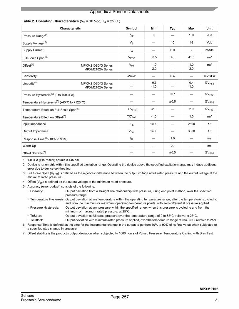
Appendix J Sensor Datasheets
Page 257

Linearity Specification Comparison
Appendix J Sensor Datasheets
Page 258

Appendix J Sensor Datasheets
Page 259

Appendix J Sensor Datasheets
Page 260

PIN 4
PIN 1
Appendix J Sensor Datasheets
Page 261

Appendix J Sensor Datasheets
Page 262

Appendix J Sensor Datasheets
Page 263

LM135/LM235/LM335, LM135A/LM235A/LM335APrecision Temperature SensorsGeneral DescriptionThe LM135 series are precision, easily-calibrated, integratedcircuit temperature sensors. Operating as a 2-terminal zener,the LM135 has a breakdown voltage directly proportional toabsolute temperature at +10 mV/˚K. With less than 1Ω dy-namic impedance the device operates over a current rangeof 400 µA to 5 mA with virtually no change in performance.When calibrated at 25˚C the LM135 has typically less than1˚C error over a 100˚C temperature range. Unlike othersensors the LM135 has a linear output.Applications for the LM135 include almost any type of tem-perature sensing over a −55˚C to +150˚C temperaturerange. The low impedance and linear output make interfac-ing to readout or control circuitry especially easy.The LM135 operates over a −55˚C to +150˚C temperaturerange while the LM235 operates over a −40˚C to +125˚C
temperature range. The LM335 operates from −40˚C to+100˚C. The LM135/LM235/LM335 are available packagedin hermetic TO-46 transistor packages while the LM335 isalso available in plastic TO-92 packages.
Featuresn Directly calibrated in ˚Kelvinn 1˚C initial accuracy availablen Operates from 400 µA to 5 mAn Less than 1Ω dynamic impedancen Easily calibratedn Wide operating temperature rangen 200˚C overrangen Low cost
Schematic Diagram
DS005698-1
November 2000LM135/LM
235/LM335,LM
135A/LM235A/LM
335APrecision
Temperature
Sensors
© 2000 National Semiconductor Corporation DS005698 www.national.com
Appendix J Sensor Datasheets
Page 264

Connection DiagramsTO-92
Plastic Package
DS005698-8
Bottom ViewOrder Number LM335Z
or LM335AZSee NS PackageNumber Z03A
SO-8Surface Mount Package
DS005698-25
Order Number LM335MSee NS PackageNumber M08A
TO-46Metal Can Package*
DS005698-26
*Case is connected to negative pin
Bottom ViewOrder Number LM135H,LM135H-MIL, LM235H,LM335H, LM135AH,
LM235AH or LM335AHSee NS PackageNumber H03HLM
135/LM235/LM335,LM135A/LM235A/LM335A
www.national.com 2
Appendix J Sensor Datasheets
Page 265

Absolute Maximum Ratings (Note 4)If Military/Aerospace specified devices are required,please contact the National Semiconductor Sales Office/Distributors for availability and specifications.
Reverse Current 15 mAForward Current 10 mAStorage TemperatureTO-46 Package −60˚C to +180˚CTO-92 Package −60˚C to +150˚CSO-8 Package −65˚C to +150˚C
Specified Operating Temp. RangeContinuous Intermittent
(Note 2)LM135, LM135A −55˚C to +150˚C 150˚C to 200˚CLM235, LM235A −40˚C to +125˚C 125˚C to 150˚CLM335, LM335A −40˚C to +100˚C 100˚C to 125˚CLead Temp. (Soldering, 10 seconds)TO-92 Package: 260˚CTO-46 Package: 300˚CSO-8 Package: 300˚CVapor Phase (60 seconds): 215˚CInfrared (15 seconds): 220˚C
Temperature Accuracy (Note 1)LM135/LM235, LM135A/LM235A
Parameter Conditions LM135A/LM235A LM135/LM235 UnitsMin Typ Max Min Typ Max
Operating Output Voltage TC = 25˚C, IR = 1 mA 2.97 2.98 2.99 2.95 2.98 3.01 VUncalibrated Temperature Error TC = 25˚C, IR = 1 mA 0.5 1 1 3 ˚CUncalibrated Temperature Error TMIN ≤ TC ≤ TMAX, IR = 1 mA 1.3 2.7 2 5 ˚CTemperature Error with 25˚C TMIN ≤ TC ≤ TMAX, IR = 1 mA 0.3 1 0.5 1.5 ˚CCalibrationCalibrated Error at Extended TC = TMAX (Intermittent) 2 2 ˚CTemperaturesNon-Linearity IR = 1 mA 0.3 0.5 0.3 1 ˚C
Temperature Accuracy (Note 1)LM335, LM335A
Parameter Conditions LM335A LM335 UnitsMin Typ Max Min Typ Max
Operating Output Voltage TC = 25˚C, IR = 1 mA 2.95 2.98 3.01 2.92 2.98 3.04 VUncalibrated Temperature Error TC = 25˚C, IR = 1 mA 1 3 2 6 ˚CUncalibrated Temperature Error TMIN ≤ TC ≤ TMAX, IR = 1 mA 2 5 4 9 ˚CTemperature Error with 25˚C TMIN ≤ TC ≤ TMAX, IR = 1 mA 0.5 1 1 2 ˚CCalibrationCalibrated Error at Extended TC = TMAX (Intermittent) 2 2 ˚CTemperaturesNon-Linearity IR = 1 mA 0.3 1.5 0.3 1.5 ˚C
Electrical Characteristics (Note 1)
LM135/LM235 LM335Parameter Conditions LM135A/LM235A LM335A Units
Min Typ Max Min Typ MaxOperating Output Voltage 400 µA≤IR≤5 mA 2.5 10 3 14 mVChange with Current At Constant TemperatureDynamic Impedance IR=1 mA 0.5 0.6 Ω
Output Voltage Temperature +10 +10 mV/˚CCoefficientTime Constant Still Air 80 80 sec
100 ft/Min Air 10 10 secStirred Oil 1 1 sec
Time Stability TC=125˚C 0.2 0.2 ˚C/khr
LM135/LM
235/LM335,LM
135A/LM235A/LM
335A
www.national.com3
Appendix J Sensor Datasheets
Page 266

Electrical Characteristics (Note 1) (Continued)
Note 1: Accuracy measurements are made in a well-stirred oil bath. For other conditions, self heating must be considered.Note 2: Continuous operation at these temperatures for 10,000 hours for H package and 5,000 hours for Z package may decrease life expectancy of the device.Note 3:
Thermal Resistance TO-92 TO-46 SO-8θJA (junction to ambient) 202˚C/W 400˚C/W 165˚C/WθJC (junction to case) 170˚C/W N/A N/ANote 4: Refer to RETS135H for military specifications.
Typical Performance CharacteristicsReverse Voltage Change
DS005698-27
Calibrated Error
DS005698-28
Reverse Characteristics
DS005698-29
Response Time
DS005698-30
Dynamic Impedance
DS005698-31
Noise Voltage
DS005698-32
Thermal ResistanceJunction to Air
DS005698-33
Thermal Time Constant
DS005698-34
Thermal Response in Still Air
DS005698-35
LM135/LM235/LM335,LM135A/LM235A/LM335A
www.national.com 4
Appendix J Sensor Datasheets
Page 267

Typical Performance Characteristics (Continued)
Application HintsCALIBRATING THE LM135Included on the LM135 chip is an easy method of calibratingthe device for higher accuracies. A pot connected across theLM135 with the arm tied to the adjustment terminal allows a1-point calibration of the sensor that corrects for inaccuracyover the full temperature range.This single point calibration works because the output of theLM135 is proportional to absolute temperature with the ex-trapolated output of sensor going to 0V output at 0˚K(−273.15˚C). Errors in output voltage versus temperature areonly slope (or scale factor) errors so a slope calibration atone temperature corrects at all temperatures.The output of the device (calibrated or uncalibrated) can beexpressed as:
where T is the unknown temperature and To is a referencetemperature, both expressed in degrees Kelvin. By calibrat-ing the output to read correctly at one temperature the outputat all temperatures is correct. Nominally the output is cali-brated at 10 mV/˚K.
To insure good sensing accuracy several precautions mustbe taken. Like any temperature sensing device, self heatingcan reduce accuracy. The LM135 should be operated at thelowest current suitable for the application. Sufficient current,of course, must be available to drive both the sensor and thecalibration pot at the maximum operating temperature aswell as any external loads.If the sensor is used in an ambient where the thermal resis-tance is constant, self heating errors can be calibrated out.This is possible if the device is run with a temperature stablecurrent. Heating will then be proportional to zener voltageand therefore temperature. This makes the self heating errorproportional to absolute temperature the same as scalefactor errors.
WATERPROOFING SENSORSMeltable inner core heat shrinkable tubing such as manufac-tured by Raychem can be used to make low-cost waterproofsensors. The LM335 is inserted into the tubing about 1⁄2"from the end and the tubing heated above the melting pointof the core. The unfilled 1⁄2" end melts and provides a sealover the device.
Typical Applications
Thermal Response in Stirred Oil Bath
DS005698-36
Forward Characteristics
DS005698-37
Basic Temperature Sensor
DS005698-2
Calibrated Sensor
DS005698-9
*Calibrate for 2.982V at 25˚C
Wide Operating Supply
DS005698-10
LM135/LM
235/LM335,LM
135A/LM235A/LM
335A
www.national.com5
Appendix J Sensor Datasheets
Page 268

Typical Applications (Continued)
Minimum Temperature Sensing
DS005698-4
Average Temperature Sensing
DS005698-18
Remote Temperature Sensing
DS005698-19
Wire length for 1˚C error due to wire drop
IR = 1mA
IR = 0.5 mA*
AWG FEET FEET14 4000 800016 2500 500018 1600 320020 1000 200022 625 125024 400 800
*For IR = 0.5 mA, the trim pot must be deleted.
Isolated Temperature Sensor
DS005698-20
LM135/LM235/LM335,LM135A/LM235A/LM335A
www.national.com 6
Appendix J Sensor Datasheets
Page 269

Typical Applications (Continued)
Simple Temperature Controller
DS005698-5
Simple Temperature Control
DS005698-21
Ground Referred Fahrenheit Thermometer
DS005698-22
*Adjust R2 for 2.554V across LM336.Adjust R1 for correct output.
Centigrade Thermometer
DS005698-23
*Adjust for 2.7315V at output of LM308
LM135/LM
235/LM335,LM
135A/LM235A/LM
335A
www.national.com7
Appendix J Sensor Datasheets
Page 270

Typical Applications (Continued)
Fahrenheit Thermometer
DS005698-24
*To calibrate adjust R2 for 2.554V across LM336.Adjust R1 for correct output.
THERMOCOUPLE COLD JUNCTION COMPENSATIONCompensation for Grounded Thermocouple
DS005698-6
*Select R3 for proper thermocouple type
THERMO- R3 SEEBECKCOUPLE (±1%) COEFFICIENT
J 377Ω 52.3 µV/˚CT 308Ω 42.8 µV/˚CK 293Ω 40.8 µV/˚CS 45.8Ω 6.4 µV/˚C
Adjustments: Compensates for both sensor and resistor tolerances1. Short LM329B2. Adjust R1 for Seebeck Coefficient times ambient temperature (in degrees K) across R3.3. Short LM335 and adjust R2 for voltage across R3 corresponding to thermocouple type
J 14.32 mV K 11.17 mVT 11.79 mV S 1.768 mV
LM135/LM235/LM335,LM135A/LM235A/LM335A
www.national.com 8
Appendix J Sensor Datasheets
Page 271

Typical Applications (Continued)
Single Power Supply Cold Junction Compensation
DS005698-11
*Select R3 and R4 for thermocouple type
THERMO- R3 R4 SEEBECKCOUPLE COEFFICIENT
J 1.05K 385Ω 52.3 µV/˚CT 856Ω 315Ω 42.8 µV/˚CK 816Ω 300Ω 40.8 µV/˚CS 128Ω 46.3Ω 6.4 µV/˚C
Adjustments:1. Adjust R1 for the voltage across R3 equal to the Seebeck Coefficient times ambient temperature in degrees Kelvin.2. Adjust R2 for voltage across R4 corresponding to thermocouple
J 14.32 mVT 11.79 mVK 11.17 mVS 1.768 mV
LM135/LM
235/LM335,LM
135A/LM235A/LM
335A
www.national.com9
Appendix J Sensor Datasheets
Page 272

Typical Applications (Continued)
Centigrade Calibrated Thermocouple Thermometer
DS005698-12
Terminate thermocouple reference junction in close proximity to LM335.Adjustments:1. Apply signal in place of thermocouple and adjust R3 for a gain of 245.7.2. Short non-inverting input of LM308A and output of LM329B to ground.3. Adjust R1 so that VOUT = 2.982V @ 25˚C.4. Remove short across LM329B and adjust R2 so that VOUT = 246 mV @ 25˚C.5. Remove short across thermocouple.
Fast Charger for Nickel-Cadmium Batteries
DS005698-13
†Adjust D1 to 50 mV greater VZ than D2.Charge terminates on 5˚C temperature rise. Couple D2 to battery.
Differential Temperature Sensor
DS005698-7
LM135/LM235/LM335,LM135A/LM235A/LM335A
www.national.com 10
Appendix J Sensor Datasheets
Page 273

Typical Applications (Continued)
Differential Temperature Sensor
DS005698-14
Variable Offset Thermometer
DS005698-15
†Adjust for zero with sensor at 0˚C and 10T pot set at 0˚C*Adjust for zero output with 10T pot set at 100˚C and sensor at 100˚COutput reads difference between temperature and dial setting of 10T pot
LM135/LM
235/LM335,LM
135A/LM235A/LM
335A
www.national.com11
Appendix J Sensor Datasheets
Page 274

Typical Applications (Continued)
Definition of TermsOperating Output Voltage: The voltage appearing acrossthe positive and negative terminals of the device at specifiedconditions of operating temperature and current.Uncalibrated Temperature Error: The error between theoperating output voltage at 10 mV/˚K and case temperatureat specified conditions of current and case temperature.
Calibrated Temperature Error: The error between operat-ing output voltage and case temperature at 10 mV/˚K over atemperature range at a specified operating current with the25˚C error adjusted to zero.
Ground Referred Centigrade Thermometer
DS005698-16
Air Flow Detector*
DS005698-17
*Self heating is used to detect air flow
LM135/LM235/LM335,LM135A/LM235A/LM335A
www.national.com 12
Appendix J Sensor Datasheets
Page 275

Physical Dimensions inches (millimeters) unless otherwise noted
Metal Can Package (H)Order Number LM135H, LM235H, LM335H, LM135AH, LM235AH or LM335AH
NS Package Number H03H
8-Lead Molded Small Outline Package (M)Order Number LM335M
NS Package Number M08A
LM135/LM
235/LM335,LM
135A/LM235A/LM
335A
www.national.com13
Appendix J Sensor Datasheets
Page 276

Physical Dimensions inches (millimeters) unless otherwise noted (Continued)
LIFE SUPPORT POLICY
NATIONAL’S PRODUCTS ARE NOT AUTHORIZED FOR USE AS CRITICAL COMPONENTS IN LIFE SUPPORTDEVICES OR SYSTEMS WITHOUT THE EXPRESS WRITTEN APPROVAL OF THE PRESIDENT AND GENERALCOUNSEL OF NATIONAL SEMICONDUCTOR CORPORATION. As used herein:
1. Life support devices or systems are devices orsystems which, (a) are intended for surgical implantinto the body, or (b) support or sustain life, andwhose failure to perform when properly used inaccordance with instructions for use provided in thelabeling, can be reasonably expected to result in asignificant injury to the user.
2. A critical component is any component of a lifesupport device or system whose failure to performcan be reasonably expected to cause the failure ofthe life support device or system, or to affect itssafety or effectiveness.
National SemiconductorCorporationAmericasTel: 1-800-272-9959Fax: 1-800-737-7018Email: [email protected]
National SemiconductorEurope
Fax: +49 (0) 180-530 85 86Email: [email protected]
Deutsch Tel: +49 (0) 69 9508 6208English Tel: +44 (0) 870 24 0 2171Français Tel: +33 (0) 1 41 91 8790
National SemiconductorAsia Pacific CustomerResponse GroupTel: 65-2544466Fax: 65-2504466Email: [email protected]
National SemiconductorJapan Ltd.Tel: 81-3-5639-7560Fax: 81-3-5639-7507
www.national.com
Plastic PackageOrder Number LM335Z or LM335AZ
NS Package Z03A
LM135/LM235/LM335,LM135A/LM235A/LM335A
PrecisionTemperatureSensors
National does not assume any responsibility for use of any circuitry described, no circuit patent licenses are implied and National reserves the right at any time without notice to change said circuitry and specifications.
Appendix J Sensor Datasheets
Page 277