guidelines for board - asset-intertech.com · board-level bs infrastructure design a simple bs...
TRANSCRIPT

Guidelines for Board Design For Test (DFT)
Based on Boundary Scan Part 1
Prepared by Ben Bennetts, DFT Consultant
for ASSET InterTech, Inc.
April 2006
ABSTRACT: This document is Part 1 of a 2-part document that contains a series of DFT Guidelines for boards to be tested
primarily through the use of boundary scan, based on the IEEE 1149.1-2001 Standard.
Any comments, corrections, suggested additions should be sent to the author, Ben Bennetts, at [email protected].

Slide 3Last revised: March, 2006
© 2006, Bennetts AssociatesASSET InterTech, Inc.
About The Author/Presenter
He is currently an Advisor to the Board of Directors of ASSET InterTech, advising the company on future directions of boundary-scan technology. He is also a core-group member of IJTAG and SJTAG (and currently the SJTAG Chairman), a co-founder and past Program Chair of the IEEE Board Test Workshop, founder of the IEEE European Board Test Workshop, and the founder and current Chairman of the IEEE’s BTTACorganisation.
Ben has published over 100 papers plus three books on test and DFT subjects.
Dr R G “Ben” Bennetts is an independent consultant in Design-For-Test (DFT), consulting in product life-cycle DFT strategies, and delivering on-site and open educational courses in DFT technologies.Previously, he has worked for LogicVision, Synopsys, GenRadand Cirrus Computers. Between 1986 and 1993, he was a free-lance consultant and lecturer on Design-for-Test (DFT) topics. During this time, he was a member of JTAG, the organization that created the IEEE 1149.1 Boundary-Scan Standard.
Slide 4Last revised: March, 2006
© 2006, Bennetts AssociatesASSET InterTech, Inc.
DFT Guidelines: Part 1
Ben Bennetts, DFT ConsultantBennetts Associates, UK
Tel: +44 1489 581276 E-mail: [email protected]://www.dft.co.uk/
Boundary-Scan Testability: Board-Level Guidelines (1)
General Guidelines
Boundary-Scan Testability: Board-Level Guidelines (1)
General Guidelines
In this document, we will look at general DFT guidelines specific to the design of boards to be tested through the
JTAG/boundary-scan registers of IEEE 1149.1-compliant devices.
© 2006, Bennetts Associates 2 April 2006 ASSET InterTech, Inc.
Slide 5Last revised: March, 2006
© 2006, Bennetts AssociatesASSET InterTech, Inc.
Board-Level DFT Guidelines
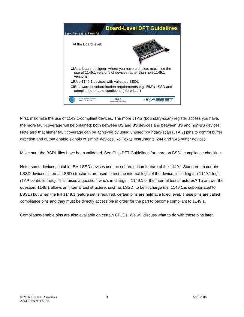
As a board designer, where you have a choice, maximise the use of 1149.1 versions of devices rather than non-1149.1 versionsUse 1149.1 devices with validated BSDLBe aware of subordination requirements e.g. IBM’s LSSD and compliance-enable conditions (more later)
At the Board level:
First, maximize the use of 1149.1-compliant devices. The more JTAG (boundary-scan) register access you have,
the more fault-coverage will be obtained: both between BS and BS devices and between BS and non-BS devices.
Note also that higher fault coverage can be achieved by using unused boundary-scan (JTAG) pins to control buffer
direction and output enable signals of simple devices like Texas Instruments’ 244 and ‘245 buffer devices.
Make sure the BSDL files have been validated. See Chip DFT Guidelines for more on BSDL compliance checking.
Note, some devices, notable IBM LSSD devices use the subordination feature of the 1149.1 Standard. In certain
LSSD devices, internal LSSD structures are used to test the internal logic of the device, including the 1149.1 logic
(TAP controller, etc). This raises a question: who’s in charge – 1149.1 or the internal test structures? To answer the
question, 1149.1 allows an internal test structure, such as LSSD, to be in charge (i.e. 1149.1 is subordinated to
LSSD) but when the full 1149.1 feature set is required, certain pins are held at a fixed level. These pins are called
compliance pins and they must be directly accessible in order for the part to become compliant to 1149.1.
Compliance-enable pins are also available on certain CPLDs. We will discuss what to do with these pins later.
© 2006, Bennetts Associates 3 April 2006 ASSET InterTech, Inc.
Slide 6Last revised: March, 2006
© 2006, Bennetts AssociatesASSET InterTech, Inc.
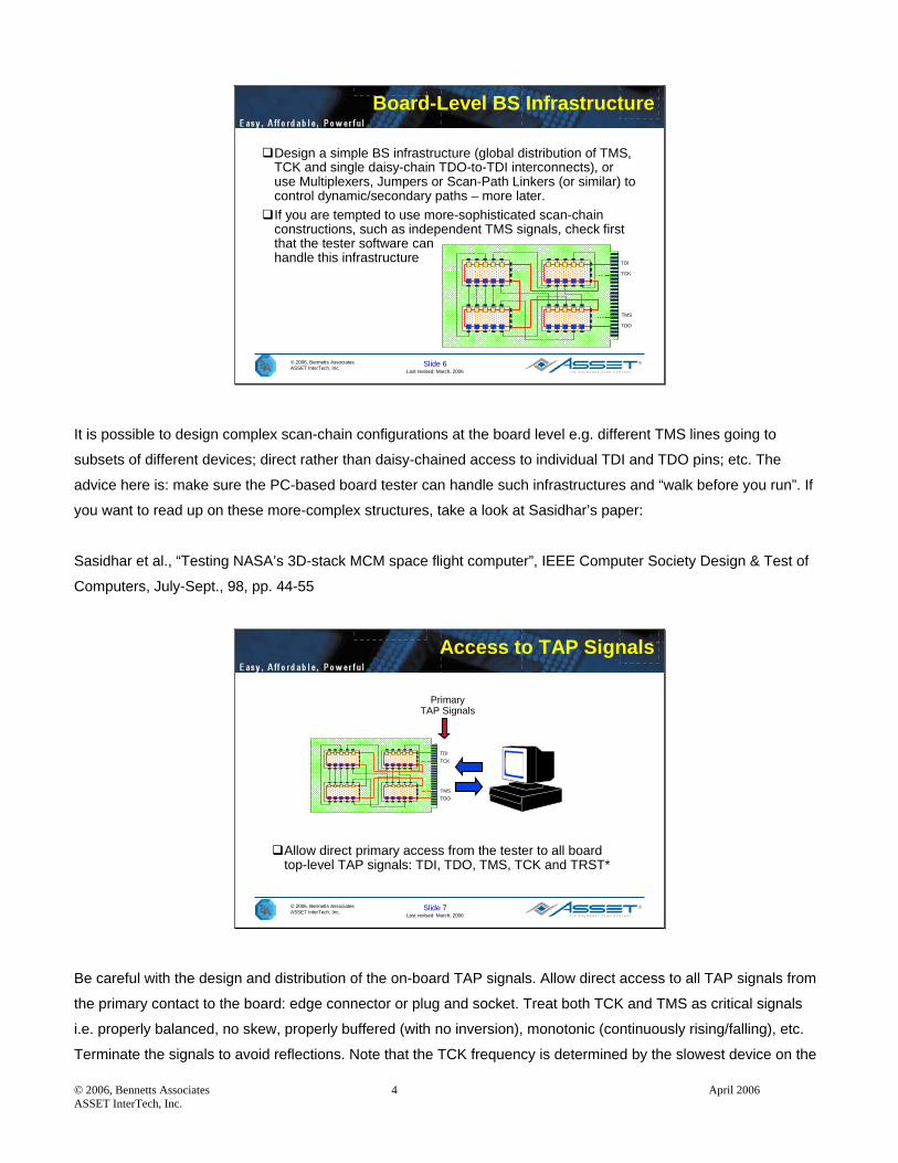
Board-Level BS Infrastructure
Design a simple BS infrastructure (global distribution of TMS, TCK and single daisy-chain TDO-to-TDI interconnects), or use Multiplexers, Jumpers or Scan-Path Linkers (or similar) to control dynamic/secondary paths – more later.If you are tempted to use more-sophisticated scan-chain constructions, such as independent TMS signals, check first that the tester software can handle this infrastructure TDI
TCK
TMS
TDO
It is possible to design complex scan-chain configurations at the board level e.g. different TMS lines going to
subsets of different devices; direct rather than daisy-chained access to individual TDI and TDO pins; etc. The
advice here is: make sure the PC-based board tester can handle such infrastructures and “walk before you run”. If
you want to read up on these more-complex structures, take a look at Sasidhar’s paper:
Sasidhar et al., “Testing NASA’s 3D-stack MCM space flight computer”, IEEE Computer Society Design & Test of
Computers, July-Sept., 98, pp. 44-55
Slide 7Last revised: March, 2006
© 2006, Bennetts AssociatesASSET InterTech, Inc.
Access to TAP Signals
Allow direct primary access from the tester to all board top-level TAP signals: TDI, TDO, TMS, TCK and TRST*
TDITCK
TMSTDO
PrimaryTAP Signals
Be careful with the design and distribution of the on-board TAP signals. Allow direct access to all TAP signals from
the primary contact to the board: edge connector or plug and socket. Treat both TCK and TMS as critical signals
i.e. properly balanced, no skew, properly buffered (with no inversion), monotonic (continuously rising/falling), etc.
Terminate the signals to avoid reflections. Note that the TCK frequency is determined by the slowest device on the
© 2006, Bennetts Associates 4 April 2006 ASSET InterTech, Inc.
board. (Maximum TCK frequency for a device is specified in the BSDL file for that device.) Place a weak pull down
on the TRST* signal – see later.
Slide 8Last revised: March, 2006
© 2006, Bennetts AssociatesASSET InterTech, Inc.
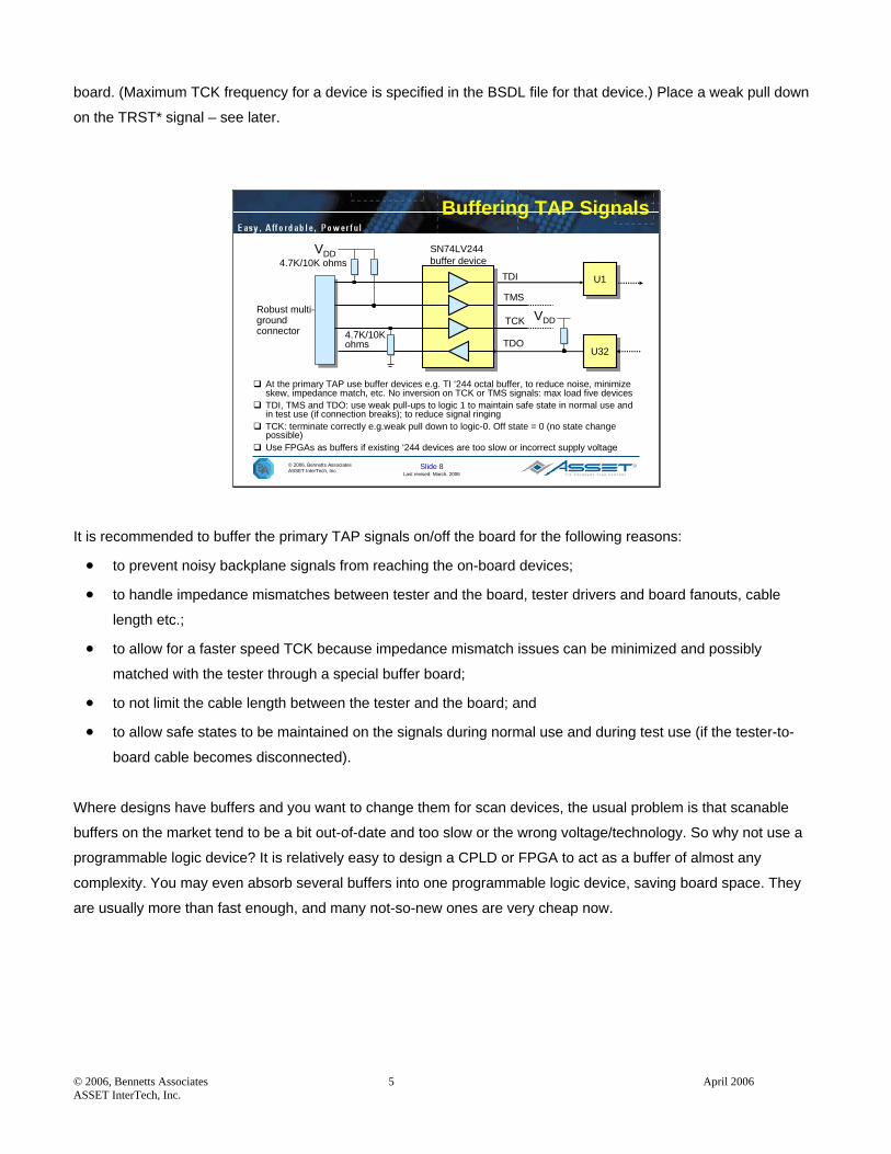
Buffering TAP Signals
At the primary TAP use buffer devices e.g. TI ‘244 octal buffer, to reduce noise, minimize skew, impedance match, etc. No inversion on TCK or TMS signals: max load five devicesTDI, TMS and TDO: use weak pull-ups to logic 1 to maintain safe state in normal use and in test use (if connection breaks); to reduce signal ringingTCK: terminate correctly e.g.weak pull down to logic-0. Off state = 0 (no state change possible)Use FPGAs as buffers if existing ‘244 devices are too slow or incorrect supply voltage
TDI
TMS
TDO
TCK
SN74LV244 buffer device4.7K/10K ohms
U1U1
U32U32
Robust multi-ground connector
VDD
4.7K/10K ohms
VDD
It is recommended to buffer the primary TAP signals on/off the board for the following reasons:
• to prevent noisy backplane signals from reaching the on-board devices;
• to handle impedance mismatches between tester and the board, tester drivers and board fanouts, cable
length etc.;
• to allow for a faster speed TCK because impedance mismatch issues can be minimized and possibly
matched with the tester through a special buffer board;
• to not limit the cable length between the tester and the board; and
• to allow safe states to be maintained on the signals during normal use and during test use (if the tester-to-
board cable becomes disconnected).
Where designs have buffers and you want to change them for scan devices, the usual problem is that scanable
buffers on the market tend to be a bit out-of-date and too slow or the wrong voltage/technology. So why not use a
programmable logic device? It is relatively easy to design a CPLD or FPGA to act as a buffer of almost any
complexity. You may even absorb several buffers into one programmable logic device, saving board space. They
are usually more than fast enough, and many not-so-new ones are very cheap now.
© 2006, Bennetts Associates 5 April 2006 ASSET InterTech, Inc.
Slide 9Last revised: March, 2006
© 2006, Bennetts AssociatesASSET InterTech, Inc.
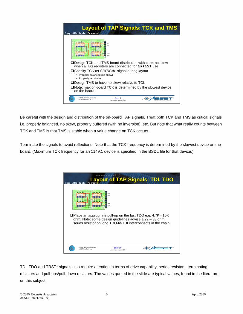
Layout of TAP Signals: TCK and TMS
Design TCK and TMS board distribution with care: no skew when all BS registers are connected for EXTEST useSpecify TCK as CRITICAL signal during layout
Properly balanced (no skew)Properly terminated
Design TMS to have no skew relative to TCKNote: max on-board TCK is determined by the slowest device on the board
TDITCK
TMSTDO
Be careful with the design and distribution of the on-board TAP signals. Treat both TCK and TMS as critical signals
i.e. properly balanced, no skew, properly buffered (with no inversion), etc. But note that what really counts between
TCK and TMS is that TMS is stable when a value change on TCK occurs.
Terminate the signals to avoid reflections. Note that the TCK frequency is determined by the slowest device on the
board. (Maximum TCK frequency for an 1149.1 device is specified in the BSDL file for that device.)
Slide 10Last revised: March, 2006
© 2006, Bennetts AssociatesASSET InterTech, Inc.
Layout of TAP Signals: TDI, TDO
Place an appropriate pull-up on the last TDO e.g. 4.7K - 10K ohm. Note: some design guidelines advise a 22 – 33 ohm series resistor on long TDO-to-TDI interconnects in the chain.
TDITCK
TMSTDO
TDI, TDO and TRST* signals also require attention in terms of drive capability, series resistors, terminating
resistors and pull-ups/pull-down resistors. The values quoted in the slide are typical values, found in the literature
on this subject.
© 2006, Bennetts Associates 6 April 2006 ASSET InterTech, Inc.

Slide 11Last revised: March, 2006
© 2006, Bennetts AssociatesASSET InterTech, Inc.
Board TRST*: Floating or Tied?
1149.1 requires TRST* internal to go high (logic-1) when left open-circuit If the master TRST* signal is left floating during normal operation andthere is no internal power-up reset to the TLR state (not mandated when TRST* is supplied), the 1149.1 TAP controller can power up in any state.
TDI
TMS
TCK
TDO
1 2 3
TRST*
Section 6.3 of the 1149.1 Standard states that, ”The TAP controller shall be forced into the Test-Logic-Reset
controller state at power-up either by use of the TRST* signal or as a result of circuitry built into the test logic”., It is
not necessary to provide an internal power-up reset if the TRST* signal has been supplied. If this is the case, what
should a designer do with TRST* lines on a board once the board has been tested and is now working normally in a
system – leave it floating or tie it low?
The 1149.1 Standard requires TRST* to go high (logic-1) when left open-circuit so that the device is tolerant to an
open-circuit fault on the TRST* pin of any 1149.1-compliant device. But, this means that if the master TRST* signal
is left floating during normal operation, the 1149.1 devices can potentially power-up in an unsafe state. One solution
is to hold TRST* constantly low while the board is operating normally. This and other solutions are discussed in the
following slides.
Note: if the TRST* signal is not incorporated into the 1149.1-compliant devices, the device must contain an internal
power-up reset and the problem does not exist.
© 2006, Bennetts Associates 7 April 2006 ASSET InterTech, Inc.

Slide 12Last revised: March, 2006
© 2006, Bennetts AssociatesASSET InterTech, Inc.
One Potential Consequence of No POR
D
Clk
Q D
Clk
Q
0
1
0
1
Data In(PI)
Scan In(SI)
ShiftDR ClockDR UpdateDR
Mode
Data Out(PO)
Scan Out(SO)
Scan Cell Hold Cell
Problem:
1. Unknown status of the Mode signal
2. Unknown content of the Hold cellBut IR Hold section should be IDCODE or BYPASS so probably OK.
Problem:
1. Unknown status of the Mode signal
2. Unknown content of the Hold cellBut IR Hold section should be IDCODE or BYPASS so probably OK.
Output goes to U?
Output goes to U?
Here, the potential problem is illustrated with the BC_1 boundary-scan cell. The output multiplexer Mode control
signal is generated by the decoded output of the Instruction register. If the register is not initialised (to the Test-
Logic Reset state), then the value of the Mode control signal could be unknown. If the Mode control line powers up
as 1, then the unknown state of the Hold Cell will be passed to the output pin.
Footnote. Strictly speaking, the Hold section of the Instruction Register should power up with the opcode for either
the IDCODE instruction (if the Identification register is present), else for the BYPASS instruction. Both these
instructions maintain the chip in its functional mode, not test mode. In functional mode, the Mode signal on a BC_1
boundary-scan cell should be logic 0, not logic 1. So, although the state of the boundary-scan (JTAG) cell may be
unknown, this unknown value should not be presented to the output pin.
© 2006, Bennetts Associates 8 April 2006 ASSET InterTech, Inc.

Slide 13Last revised: March, 2006
© 2006, Bennetts AssociatesASSET InterTech, Inc.
Solution #1: Power-Up Reset on Board
TDI
TMS
TCK
TDO
2 31
Power-UpReset CircuitPower-Up
Reset Circuit
TRST*
One solution is an automatic power-up reset circuit on the board. This solution is simple but usually not used. The
next slide shows the most common solution.
Slide 14Last revised: March, 2006
© 2006, Bennetts AssociatesASSET InterTech, Inc.
Solution #2: Board Pull-Down Resistance
TDI
TMS
TCK
TDO
1 2 3
R (~10K ohm)
On-BoardPull-Down Resistor
On-BoardPull-Down Resistor
TRST*
Note: place the pull-down resistor upstream of the buffer. Do not place individual pull-downs at each TRST* signal pin.
Another solution is to place a weak pull down (typically around 10K ohm) on the TRST* line that
• overcomes the parallel sum of the device internal pull ups, and
• is easily driven high by a PC-based Board tester.
This solution is common and used by Motorola (see ITC2000, Paper 2.3) but the value of the pull-down resistor is
critical if there is no buffer on the TRST* signal input. Too low, and a PC-based driver may not be able to drive
© 2006, Bennetts Associates 9 April 2006 ASSET InterTech, Inc.

TRST* high enough to be sensed reliably as a logic 1 by all boundary-scan TRST* inputs. Too high, and the board
will contain a voltage divider that may drain considerable power from, say, a battery power-supply system.
Note, when the board contains a very large number of JTAG/boundary-scan devices with the TRST* signal
provided, the parallel sum of the internal TRST* pull-ups will become very low. Under these conditions, it is
recommended to use a buffer to drive the primary TRST* signal onto the multiple TRST* signals and then to place
the pull-down resistor on the primary side of the buffer, as shown in the Figure above. This solution removes the
objections above.
Slide 15Last revised: March, 2006
© 2006, Bennetts AssociatesASSET InterTech, Inc.
Solution #3: Internal POR Circuit
TDI
TMS
TCK
TDO
1 2 3
TRST*
Adding a Power-On-Reset (POR) circuit inside each 1149.1-compliant device will also solve the problem but it requires all 1149.1 devices to include the POR.
If each 1149.1-compliant device contains a Power-On-Reset (to the Test-Logic/Reset state), then the problem goes
away. But, every device in the chain, including those devices without a TRST* signal, has to have this facility for it
to work correctly at board level.
© 2006, Bennetts Associates 10 April 2006 ASSET InterTech, Inc.

Slide 16Last revised: March, 2006
© 2006, Bennetts AssociatesASSET InterTech, Inc.
Testing The Tester: Resolving Opens
“Testing the tester” via IR-Scan or DR-Scan can lead to ambiguous diagnosis if there is an open on a TDO-to-TDI interconnect.“Solution: add test points or flying probe/in-circuit nails onto these interconnects
TDI
TMS
TCK
TDO
1 2 3
TRST*
Testing the tester can be done either by an IR-Scan or a DR-Scan. IR-Scan places the Instruction register between
TDI and TDO and then captures and shifts out the internal hard-wired 01 in the two least significant bits of the
register. DR-Scan places the Identification register, if present, else Bypass register between TDI and TDO and then
captures and shifts out the internal hard-wired values (1 + 31 bits for Identification, 0 for Bypass). If there is an open
circuit between a TDO-out and the next TDI-in, it is not possible to identify at what end the open has occurred.
Consequently, the diagnosis is to both devices. Placing a test point or flying probe/in-circuit nail on these
interconnects is a simple solution that allows the open to be located to just one of the devices.
Slide 17Last revised: March, 2006
© 2006, Bennetts AssociatesASSET InterTech, Inc.
Tying-Off Control Pins
TAPController
Instructionregister
Boundary-ControlRegister
BypassRegister
IdentificationRegister
Boundary-Scan Register
TDI TDO
TCK
TMS
TI SN74LVTH18502ADevice Function:18 bidirectional
Transceiver Channels+
12 control pins
A1 (1:9)
B2 (1:9)A2 (1:9)
B1 (1:9)OEBA_NEG1
OEBA_NEG2
OEAB_NEG1
OEAB_NEG2
Use weak pull-ups/downs for tied-of pins, not direct connection to Power or Ground. This allows the pin to be pulled against the resistor in test mode
Use weak pull-ups/downs for tied-of pins, not direct connection to Power or Ground. This allows the pin to be pulled against the resistor in test mode
VDD
Or unusedBS output
If bidirectional (IO) or three-state (OZ) control pins are tied-off at board level, tie off with a weak pull-up or pull-down
resistor rather than connect direct to the Power or Ground rails. This allows an ICT/FPT nail to be used during test
© 2006, Bennetts Associates 11 April 2006 ASSET InterTech, Inc.

mode to change the status of the pins, plus it allows detection of a missing or open-circuit resistor through a simple
parametric test.
Slide 18Last revised: March, 2006
© 2006, Bennetts AssociatesASSET InterTech, Inc.
Board-Level Ground Bounce
Assess the possibility of ground bounce at the board level during application of EXTEST patterns.
Update_DR drives simultaneous value changes onto input and output driversToo many simultaneous changes may cause transients on power or groundCheck max Simultaneous Switching Output Limit (SSOL)Note: individual 1149.1 devices should be tolerant of internal ground bounce but this does not guarantee that the board is also tolerant of ground bounce
TDI20 x Driver (TX) boundary-scan cells
TDO
20 x Sensor (RX) boundary-scan cells
200-to-1
or1-to-0
changes
Although each 1149.1-compliant device should not exhibit internal ground bounce under worst-case switching
conditions, there is no guarantee that ground bounce will not happen at board level when all devices are switching
worst-case. Some PC-based testers are able to accept a specification for a maximum Simultaneous Switching
Output Limit (SSOL) and to constrain the interconnect pattern-generator to conform to this limit but note that this is
really not a JTAG/boundary-scan issue. It is more a general board-design issue and the responsibility is with the
board designer to ensure no ground-bounce problems for the board no matter what operational mode the board is
in – functional or test.
Note: Most big FPGAs state in their data sheet that they cannot support switching of more than a specified number
of cells at once. They have so many cells (some pushing 3,000) that the infrastructure to support switching all at
once is not practical.
© 2006, Bennetts Associates 12 April 2006 ASSET InterTech, Inc.

Slide 19Last revised: March, 2006
© 2006, Bennetts AssociatesASSET InterTech, Inc.
Achieving SSOL Constraints
C U
C U
C U
C U
C U
C U
C U
C U
Net 1
Net 2
Net 3
Net 4
Chip 1 Chip 23 2
21
0
0
0
0
0 0 1
0 1 0
0 1 1
1 0 0
P1P2P3Patterns P2a
Three patterns, P1, P2 and P3, based on the standard counting algorithm produce a SSO of 2 (50%) between P1 and P2, and an SSO of 3 (75%) between P2 and P3. Assume SSO/> 50%
In the 4-interconnect example above, the patterns have been assigned based on the Counting Algorithm – straight
up count.
Assume SSOL = 2 i.e. no more than 50% of the boundary-scan or JTAG cells can switch simultaneously
The Counting Algorithm breaks the 50% constraint limit between Pattern 2 and Pattern 3 if Pattern 3 follows the
vertical counting pattern of 0001.
Extra test, P2a = 0000, is added to reduce SSOs between pattern 2 and Pattern 3 to 2 and 1 respectively.
© 2006, Bennetts Associates 13 April 2006 ASSET InterTech, Inc.
Slide 20Last revised: March, 2006
© 2006, Bennetts AssociatesASSET InterTech, Inc.
Achieving SSOL Constraints
C U
C U
C U
C U
C U
C U
C U
C U
Net 1
Net 2
Net 3
Net 4
0 0 1
0 1 0
0 1 1
1 0 0
Chip 1 Chip 2
1
3 22
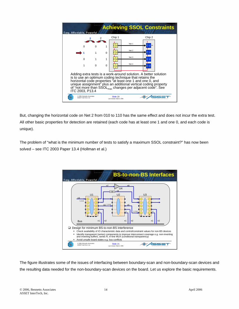
Adding extra tests is a work-around solution. A better solution is to use an optimum coding technique that retains the horizontal code properties “at least one 1 and one 0, and unique assignment” plus an additional vertical coding property of “not more than SSOLmax changes per adjacent code”. See ITC 2003, P13.4
But, changing the horizontal code on Net 2 from 010 to 110 has the same effect and does not incur the extra test.
All other basic properties for detection are retained (each code has at least one 1 and one 0, and each code is
unique).
The problem of “what is the minimum number of tests to satisfy a maximum SSOL constraint?” has now been
solved – see ITC 2003 Paper 13.4 (Hollman et al.)
Slide 21Last revised: March, 2006
© 2006, Bennetts AssociatesASSET InterTech, Inc.
BS-to-non-BS Interfaces
Design for minimum BS-to-non-BS interference Check availability of IO characteristic data and control/constraint values for non-BS devicesIdentify transparent (series) components to improve interconnect coverage e.g. non-inverting and inverting buffers, series R, in-line MUX (conditional transparency)Avoid unsafe board states e.g. bus conflicts
IO IOIO
O_Enab
Bus
O_Enab
O_Enab
U1 U2 U3
U4
n1 n2 n1 n2 n1 n2
n3
n4 n5
n6
n7 n8
R
The figure illustrates some of the issues of interfacing between boundary-scan and non-boundary-scan devices and
the resulting data needed for the non-boundary-scan devices on the board. Let us explore the basic requirements.
© 2006, Bennetts Associates 14 April 2006 ASSET InterTech, Inc.

The Interconnect pattern-generation algorithm will have no awareness of the nature of any other non-boundary-
scan device attached to JTAG/boundary-scan controlled or observed nets. Therefore, we have to supply some
basic information about these devices. For example, are the non-boundary-scan pins inputs (I), outputs (O), tristate
outputs (OZ) or bidirectional (IO)? This data, simple to determine, is called characteristic data or cluster-model
data. In the example above, we will need to supply characteristic data files for the non-boundary-scan devices U2
and U4.
In the case of tristate and bidirectional pins, we need to know what logic values on what pins will control the status
of these pins so that, if necessary, we can put them into a safe high-Z or input-mode state (no bus conflict). This
data is known as constraint data. In the example above, we will need to constrain the bidirectional pins of U2 to be
inputs rather than outputs during interconnect test. This will be achieved by a constraint value on U2’s O_Enab
signal.
Finally, certain non-boundary-scan devices, such as a series resistor or a line driver (U4 above), have a useful
property called transparency – that is, logic values on the inputs are passed to the outputs with no change. If the
interconnect pattern-generator knows about this property, then it may be able to treat two separate nets (n7 and n8
above) as one continuous net and drive test patterns across the single net, thereby increasing the coverage. Make
sure all characteristic data for non-BS devices are available, including transparent properties and enabling pins and
control value for three-state (OZ) and bidirectional (IO) pins.
Slide 22Last revised: March, 2006
© 2006, Bennetts AssociatesASSET InterTech, Inc.
Controlling NBS-Device Output Enables
IO IOIO
O_Enab
Bus
O_Enab
O_Enab
U1 U2 U3
U4
n1 n2 n1 n2 n1 n2
n3
n4 n5
n6
n7 n8
R
Maximise the use of un-used boundary-scan cells and/or physical nails during board test
To control the outputs of non-BS devices e.g. by non-BS device O_Enab pinsTo receive inputs from non-BS devices
A general guideline that comes out of the previous discussion is to make sure that pin-status control signals for
non-boundary-scan devices can be controlled: either directly from the edge connector, or by a physical ICT/FPT
nail, or by an unused JTAG/boundary-scan cell.
© 2006, Bennetts Associates 15 April 2006 ASSET InterTech, Inc.

Slide 23Last revised: March, 2006
© 2006, Bennetts AssociatesASSET InterTech, Inc.
Beware Unsafe Board States
Chip_Select
Chip_Select
Chip_Select
RAM1
RAM3
RAM2
Bus
0
0
1
1
0
Z
EXTEST: use constraintsPRELOAD + CLAMPDirect control thru flying probe/ICT nails
During interconnect test, boundary-scan or JTAG devices are in test mode (EXTEST instruction). If a boundary-
scan or JTAG device in test mode happens also to be connected to a non-boundary-scan device, the values driven
into the non-boundary-scan device are coming from the JTAG/boundary-scan cells and are the values created by
the interconnect pattern-generator. These values have the potential to damage the non-boundary-scan device and
the board should be designed to prevent this from happening.
The example above shows three non-boundary-scan RAMs whose Chip-Select control inputs are connected to
three outputs of a JTAG or boundary-scan device. If the three boundary-scan/JTAG cells are unconstrained, there
is a high probability that any two or all three RAMs will be selected simultaneously, thus creating a bus conflict.
One solution is to include the hold section in the boundary-scan cell (as in the BC_1) and to use the EXTEST
instruction to load continuously safe values (known as constraint values) into the hold sections of these three cells.
Alternatively, a set of safe values could be set up by the PRELOAD instruction and applied through the CLAMP
instruction, leaving the JTAG or boundary-scan device with its BYPASS register selected. Yet another solution
would be to provide an external control on the Chip-Select lines and drive the outputs to their high-Z state.
As an aside, it is worth noting that many BSDL files define X to be the safe state on Tristate and Bidirectional pins.
In reality, there is no such thing as an X state and the value will default to either 1 or 0. This value is usually
program-generation software specific. To avoid surprises, the designer should check that either interpretation of X
will not cause damage to driven devices.
© 2006, Bennetts Associates 16 April 2006 ASSET InterTech, Inc.

Slide 24Last revised: March, 2006
© 2006, Bennetts AssociatesASSET InterTech, Inc.
Loop-Back Connector Test
Scan cells to/from a board connector cannot be tested for open-circuits.Solution: use a connector loop-back fixture or a simple 1149.1 device.
1
Connector e.g Ethernet, RS 232, etc
Are there any boundary scan devices connected directly to an edge connector? If so, can a loop-back test be used
to check for opens between the scan cells and the connector pins? Alternatively, can you plug into a dummy 1149.1
device for testing purposes?
Slide 25Last revised: March, 2006
© 2006, Bennetts AssociatesASSET InterTech, Inc.
Different Voltage Levels
Ideally, group devices with the same voltage levels into the same scan chain ...… or provide voltage converters between different parts of the scan chain
TDI
TMS
TCK
TDO
1 2 3
TRST*
3.3Vto
1.8V
1.8Vto
3.3V
3.3V 3.3V 1.8V
Optional
Devices on the same board with different voltage levels should be grouped and master TAP signals distributed
globally passing through appropriate voltage-level converters. That way, full interconnect tests can still be applied.
Note: final TDO off the board may need to be converted back to the same level as the initial TDI, TMS and TCK
levels. It depends on the flexibility of the interface pod.
© 2006, Bennetts Associates 17 April 2006 ASSET InterTech, Inc.
Slide 26Last revised: March, 2006
© 2006, Bennetts AssociatesASSET InterTech, Inc.
Handling Non-Compliant Devices
Place a zero-ohm jumper between TDI and TDO of suspected non-compliant or boundary-scan non-operational devices in order to bypass them if necessary.Make sure TMS is disconnected to ensure that the non-compliant device is held in its Test-Logic Reset state (TMS = 1 when open circuit).
TDI
TMSTCK
TDO
1 2 3
TRST*
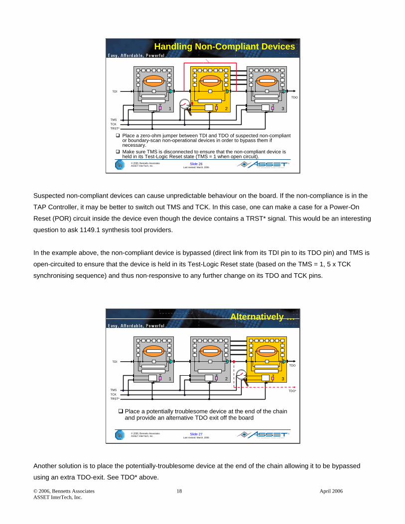
Suspected non-compliant devices can cause unpredictable behaviour on the board. If the non-compliance is in the
TAP Controller, it may be better to switch out TMS and TCK. In this case, one can make a case for a Power-On
Reset (POR) circuit inside the device even though the device contains a TRST* signal. This would be an interesting
question to ask 1149.1 synthesis tool providers.
In the example above, the non-compliant device is bypassed (direct link from its TDI pin to its TDO pin) and TMS is
open-circuited to ensure that the device is held in its Test-Logic Reset state (based on the TMS = 1, 5 x TCK
synchronising sequence) and thus non-responsive to any further change on its TDO and TCK pins.
Slide 27Last revised: March, 2006
© 2006, Bennetts AssociatesASSET InterTech, Inc.
Alternatively …
Place a potentially troublesome device at the end of the chain and provide an alternative TDO exit off the board
TDI
TMSTCK
TDO
1 2 3
TRST*
TDO*
Another solution is to place the potentially-troublesome device at the end of the chain allowing it to be bypassed
using an extra TDO-exit. See TDO* above.
© 2006, Bennetts Associates 18 April 2006 ASSET InterTech, Inc.
Slide 28Last revised: March, 2006
© 2006, Bennetts AssociatesASSET InterTech, Inc.
Using Un-Used Boundary-Scan Cells
Using two unused boundary-scan cells to control system clock distribution to reduce noise, for example.Very useful during prototype board debug
Clock distribution
Osc A
Osc B
En A
Out A1Out A2Out A3Out A4Out B1Out B2Out B3Out B4
En B
1
In A
In B
VSS
E.g. Un-used FPGA pins
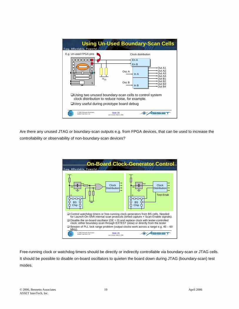
Are there any unused JTAG or boundary-scan outputs e.g. from FPGA devices, that can be used to increase the
controllability or observability of non-boundary-scan devices?
Slide 29Last revised: March, 2006
© 2006, Bennetts AssociatesASSET InterTech, Inc.
On-Board Clock-Generator Control
Control watchdog timers or free-running clock generators from BS cells. Needed for Launch-On-Shift internal scan protocols (timed capture + Scan-Enable signals).Disable the on-board oscillator (OE = 0) and replace clock with tester-controlled clock: either boundary-scan through EXTEST (slow) or directly from the testerBeware of PLL lock range problem (output clocks work across a range e.g. 45 – 60 MHz).
ClockDistributionOE
Out
BSChip
0
ClockDistributionOE
Out
BSChip
0 Test-Enab
Free-running clock or watchdog timers should be directly or indirectly controllable via boundary-scan or JTAG cells.
It should be possible to disable on-board oscillators to quieten the board down during JTAG (boundary-scan) test
modes.
© 2006, Bennetts Associates 19 April 2006 ASSET InterTech, Inc.
Slide 30Last revised: March, 2006
© 2006, Bennetts AssociatesASSET InterTech, Inc.
Allow Defeatable Tied-Off Control Pins
Chip_Select
Bus
ZChip 1
Chip 2
Weak pull-down
or unused BS cell Functional mode:• Chip 1: outputs active• Chip 2: bidirects
always inputsTest Mode:• Chip 1: outputs highZ• Chip 2: bidirects
either outputs or inputs e.g BC_7s
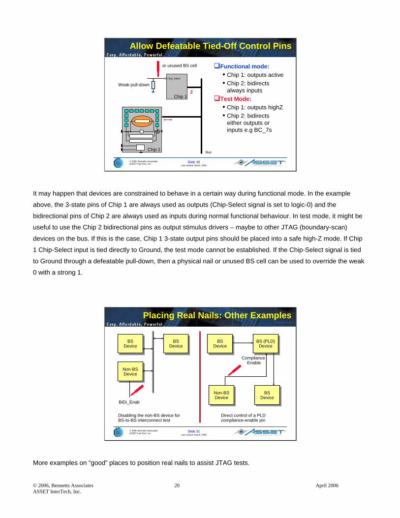
It may happen that devices are constrained to behave in a certain way during functional mode. In the example
above, the 3-state pins of Chip 1 are always used as outputs (Chip-Select signal is set to logic-0) and the
bidirectional pins of Chip 2 are always used as inputs during normal functional behaviour. In test mode, it might be
useful to use the Chip 2 bidirectional pins as output stimulus drivers – maybe to other JTAG (boundary-scan)
devices on the bus. If this is the case, Chip 1 3-state output pins should be placed into a safe high-Z mode. If Chip
1 Chip-Select input is tied directly to Ground, the test mode cannot be established. If the Chip-Select signal is tied
to Ground through a defeatable pull-down, then a physical nail or unused BS cell can be used to override the weak
0 with a strong 1.
Slide 31Last revised: March, 2006
© 2006, Bennetts AssociatesASSET InterTech, Inc.
Placing Real Nails: Other Examples
BSDeviceBS
Device
Non-BSDevice
Non-BSDevice
BSDeviceBS
Device
BiDi_Enab
Disabling the non-BS device forBS-to-BS interconnect test
BSDeviceBS
DeviceBS (PLD)
DeviceBS (PLD)
Device
Compliance Enable
Direct control of a PLD compliance-enable pin
BSDeviceBS
DeviceNon-BSDevice
Non-BSDevice
More examples on “good” places to position real nails to assist JTAG tests.
© 2006, Bennetts Associates 20 April 2006 ASSET InterTech, Inc.

Slide 32Last revised: March, 2006
© 2006, Bennetts AssociatesASSET InterTech, Inc.
Use of Physical Nails: Summary
Consider placing Flying Probe/ICT nails on:Non-BS device Output-Enable, BiDi-Enable signalsBoundary-scan signals of emulatable devices (for monitoring)Any special control signals needed to effect compliance or otherwise activate boundary-scan modesAny signals that de-activate non-BS devices attached to a BS-to-BS interconnect (to simplify interconnect test)IO signals of RAMs and non-BS flash devices and the disabling signals of the non-BS devices connected to these IO signals (for quicker control sequences)TDO-to-TDI interconnects (to assist scan-chain diagnosis)Any other signals required for a non-BS test e.g. defeatable pull-ups/pull-downs, etc.
© 2006, Bennetts Associates 21 April 2006 ASSET InterTech, Inc.