grounding in high speed systems walt kester, james …...d a a gnd dn ia id a b = analog grounda...
TRANSCRIPT
1
GROUNDING IN HIGH SPEED SYSTEMS
Walt Kester, James Bryant
The importance of maintaining a low impedance large area ground plane is criticalto practically all analog circuits today, especially at high speeds. The ground planenot only acts as a low impedance return path for high frequency currents but alsominimizes EMI/RFI emissions. Because of the shielding action of the ground plane,the circuits susceptibility to external EMI/RFI is also reduced.
All IC ground pins should be soldered directly to the ground plane to minimize seriesinductance. Power supply pins should be decoupled to the ground plane using lowinductance ceramic surface mount capacitors. If through-hole mounted ceramiccapacitors must be used, their leads should be less than 1mm. Ferrite beads may bealso required.
The ground plane allows the impedance of PCB traces to be controlled, and highfrequency signals can be terminated in the characteristic impedance of the trace tominimize reflections when necessary.
Each PCB in the system should have at least one complete layer dedicated to theground plane. Ideally, a double-sided board should have one side dedicated toground and the other side for interconnections. In practice, this is not possible, sincesome of the ground plane will certainly have to be removed to allow for signal andpower crossovers and vias. Nevertheless, as much area as possible should bepreserved, and at least 75% should remain. After completing an initial layout, theground layer should be checked carefully to make sure there are no isolated ground"islands." IC ground pins located in a ground "island" have no current return path tothe ground plane.
The best way of minimizing ground impedance in a multicard system is to useanother PCB as a backplane for interconnections between cards, thus providing acontinuous ground plane to the mother card. The PCB connector should have atleast 30-40% of its pins devoted to ground, and these pins should be connected to theground plane on the backplane mother card. To complete the overall systemgrounding scheme there are two possibilities: (1) The backplane ground plane can beconnected to chassis ground at numerous points, thereby diffusing the variousground current return paths. (2) The ground plane can be connected to a singlesystem "star ground" point (generally at the power supply).
The first approach is often used at very high frequencies and where the returncurrents are relatively constant. The low ground impedance is maintained all theway through the PC boards, the backplane, and ultimately the chassis. It is criticalthat good electrical contact be made where the grounds are connected to the sheetmetal chassis. This requires self-tapping sheet metal screws or "biting" washers.Special care must be taken where anodized aluminum is used for the chassismaterial, since its surface acts as an insulator.
In other systems, especially high speed ones with large amounts of digital circuitry,it is highly desirable to physically separate sensitive analog components from noisydigital components. It is usually desirable to use separate ground planes for theanalog and the digital circuitry. On PCBs which have both analog and digital
2
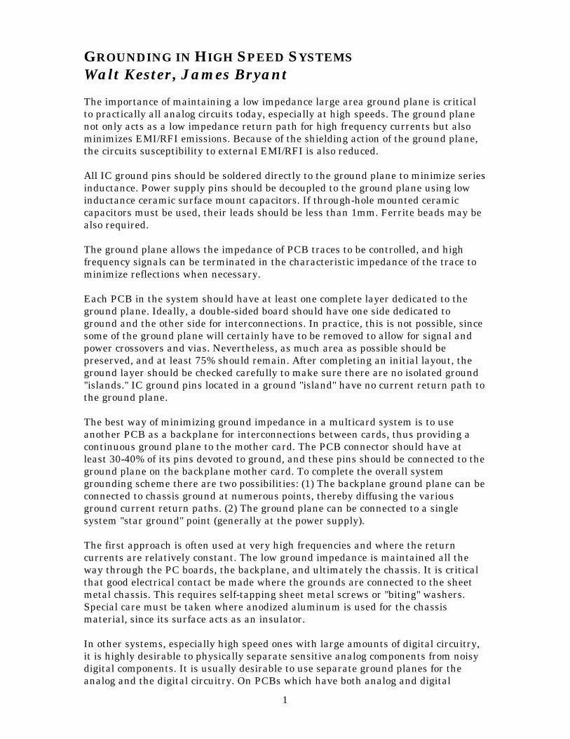
circuits, there are two separate ground planes. These planes should not overlap inorder to minimize capacitive coupling between the two. The separate analog anddigital ground planes are continued on the backplane using either motherboardground planes or "ground screens" which are made up of a series of wiredinterconnections between the connector ground pins. The arrangement shown inFigure 7.26 illustrates that the two planes are kept separate all the way back to acommon system "star" ground, generally located at the power supplies. Theconnections between the ground planes, the power supplies, and the "star" should bemade up of multiple bus bars or wide copper brads for minimum resistance andinductance. The back-to-back Schottky diodes on each PCB are inserted to preventaccidental DC voltage from developing between the two ground systems when cardsare plugged and unplugged.
a
SEPARATING ANALOG AND DIGITAL GROUNDS
7.26
SYSTEM STARGROUND
POWERSUPPLIES
ANALOG GND PLANE
DIGITAL GND PLANE
BACKPLANE
DIGITALGROUNDPLANE
ANALOGGROUNDPLANE
DIGITALGROUNDPLANE
ANALOGGROUNDPLANE
PCB
A D A
VA
VD
PCB
VDVAVDVA
D
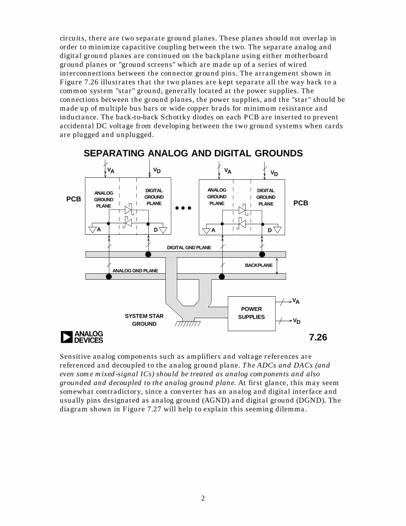
Sensitive analog components such as amplifiers and voltage references arereferenced and decoupled to the analog ground plane. The ADCs and DACs (andeven some mixed-signal ICs) should be treated as analog components and alsogrounded and decoupled to the analog ground plane. At first glance, this may seemsomewhat contradictory, since a converter has an analog and digital interface andusually pins designated as analog ground (AGND) and digital ground (DGND). Thediagram shown in Figure 7.27 will help to explain this seeming dilemma.
3
7.27
PROPER GROUNDING OF ADCs, DACs,AND OTHER MIXED-SIGNAL ICs
a
"QUIET"DIGITAL BUFFER
LATCH
NOISYDATA BUS
= DIGITAL GROUND PLANE
DA
AGND DGND
IA ID
BA
= ANALOG GROUND PLANE
ANALOGIN/OUT
CSTRAY
CSTRAY
VA VDA
A D
ADC,ORDAC
VA
A
∆∆V
D
D
A
ANALOGCIRCUITS
DIGITALCIRCUITS
A
Inside an IC that has both analog and digital circuits, such as an ADC or a DAC, thegrounds are usually kept separate to avoid coupling digital signals into the analogcircuits. Figure 7.27 shows a simple model of a converter. There is nothing the ICdesigner can do about the wirebond inductance and resistance associated withconnecting the pads on the chip to the package pins except to realize it's there. Therapidly changing digital currents produce a voltage at point B which will inevitablycouple into point A of the analog circuits through the stray capacitance, CSTRAY. Inaddition, there is approximately 0.2pF unavoidable stray capacitance between everypin of the IC package! It's the IC designer's job to make the chip work in spite ofthis. However, in order to prevent further coupling, the AGND and DGND pinsshould be joined together externally to the analog ground plane with minimum leadlengths. Any extra impedance in the DGND connection will cause more digital noiseto be developed at point B; it will, in turn, couple more digital noise into the analogcircuit through the stray capacitance.
The name "DGND" on an IC tells us that this pin connects to the digital ground of theIC. This does not imply that this pin must be connected to the digital ground of thesystem.
It is true that this arrangement will inject a small amount of digital noise on theanalog ground plane. These currents should be quite small, and can be minimized byensuring that the converter input/or output does not drive a large fanout (theynormally can't by design). Minimizing the fanout on the converter's digital port willalso keep the converter logic transitions relatively free from ringing, and therebyminimize any potential coupling into the analog port of the converter. The logic
4
supply pin (VD) can be further isolated from the analog supply by the insertion of asmall lossy ferrite bead as shown in Figure 7.27. The internal digital currents of theconverter will return to ground through the VD pin decoupling capacitor (mountedas close to the converter as possible) and will not appear in the external groundcircuit. It is always a good idea (as shown in Figure 7.27) to place a buffer latchadjacent to the converter to isolate the converter's digital lines from any noise whichmay be on the data bus. Even though a few high speed converters have three-stateoutputs/inputs, this isolation latch represents good design practice.
The buffer latch and other digital circuits should be grounded and decoupled to thedigital ground plane of the PC board. Notice that any noise between the analog anddigital ground plane reduces the noise margin at the converter digital interface.Since digital noise immunity is of the orders of hundreds or thousands of millivolts,this is unlikely to matter.
7.28
POWER SUPPLY, GROUNDING, AND DECOUPLING POINTS
a
= DIGITAL GROUND PLANE
= ANALOG GROUND PLANEA
D
A BUFFERLATCH
TO OTHERDIGITALCIRCUITS
ADCOR
DAC
A A A
AAA
A
AA
VAVA VD
D
D
VA
VAVD
DGNDAGND
VA
VOLTAGEREFERENCE
SAMPLINGCLOCK
GENERATOR
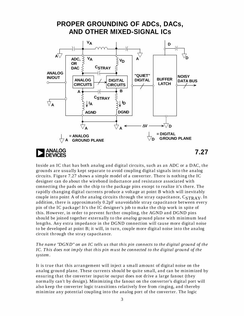
Separate power supplies for analog and digital circuits are also highly desirable. Theanalog supply should be used to power the converter. If the converter has a pindesignated as a digital supply pin (VD), it should either be powered from a separateanalog supply, or filtered as shown in the diagram. All converter power pins shouldbe decoupled to the analog ground plane, and all logic circuit power pins should bedecoupled to the digital ground plane. If the digital power supply is relatively quiet,it may be possible to use it to supply analog circuits as well, but be very cautious.The sampling clock generation circuitry should also be grounded and heavily-decoupled to the analog ground plane. As previously discussed, phase noise on thesampling clock produces degradation in system SNR.
A low phase-noise crystal oscillator should be used to generate the ADC samplingclock, because sampling clock jitter modulates the input signal and raises the noise
5
and distortion floor. The sampling clock generator should be isolated from noisydigital circuits and grounded and decoupled to the analog ground plane, as is truefor the op amp and the ADC.
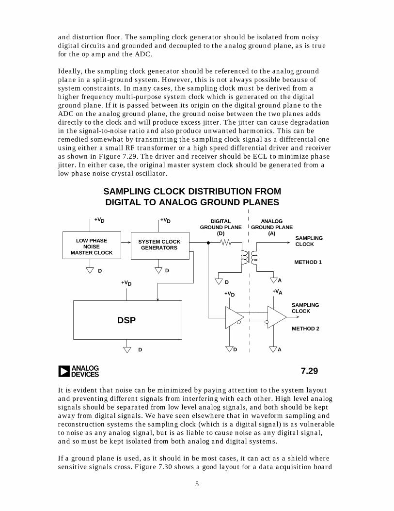
Ideally, the sampling clock generator should be referenced to the analog groundplane in a split-ground system. However, this is not always possible because ofsystem constraints. In many cases, the sampling clock must be derived from ahigher frequency multi-purpose system clock which is generated on the digitalground plane. If it is passed between its origin on the digital ground plane to theADC on the analog ground plane, the ground noise between the two planes addsdirectly to the clock and will produce excess jitter. The jitter can cause degradationin the signal-to-noise ratio and also produce unwanted harmonics. This can beremedied somewhat by transmitting the sampling clock signal as a differential oneusing either a small RF transformer or a high speed differential driver and receiveras shown in Figure 7.29. The driver and receiver should be ECL to minimize phasejitter. In either case, the original master system clock should be generated from alow phase noise crystal oscillator.
a
SAMPLING CLOCK DISTRIBUTION FROMDIGITAL TO ANALOG GROUND PLANES
7.29
DIGITALGROUND PLANE
(D)
+VD ANALOGGROUND PLANE
(A)SAMPLINGCLOCK
SAMPLINGCLOCK
+VD
+VD
+VD+VA
A
A
D
D
DD
D
LOW PHASENOISE
MASTER CLOCK
SYSTEM CLOCKGENERATORS
DSP
METHOD 1
METHOD 2
It is evident that noise can be minimized by paying attention to the system layoutand preventing different signals from interfering with each other. High level analogsignals should be separated from low level analog signals, and both should be keptaway from digital signals. We have seen elsewhere that in waveform sampling andreconstruction systems the sampling clock (which is a digital signal) is as vulnerableto noise as any analog signal, but is as liable to cause noise as any digital signal,and so must be kept isolated from both analog and digital systems.
If a ground plane is used, as it should in be most cases, it can act as a shield wheresensitive signals cross. Figure 7.30 shows a good layout for a data acquisition board

6
where all sensitive areas are isolated from each other and signal paths are kept asshort as possible. While real life is rarely as tidy as this, the principle remains avalid one.
7.30
A PC BOARD LAYOUT SHOWING GOOD SIGNAL ROUTING
a
SAMPLING CLOCKGENERATOR
POWER
ANALOGINPUT
MULTIPLEGROUNDS
DATABUS
ADDRESSBUS
MULTIPLEGROUNDS
ADC
FILTER
AMPLIFIER
DSP
BUFFERLATCH
CONTROLLOGIC
DEMULTIPLEXER
BUFFERMEMORY
REF
TIMINGCIRCUITS
There are a number of important points to be considered when making signal andpower connections. First of all a connector is one of the few places in the systemwhere all signal conductors must run parallel - it is therefore a good idea to separatethem with ground pins (creating a faraday shield) to reduce coupling between them.
Multiple ground pins are important for another reason: they keep down the groundimpedance at the junction between the board and the backplane. The contactresistance of a single pin of a PCB connector is quite low (of the order of 10 mOhms)when the board is new - as the board gets older the contact resistance is likely torise, and the board's performance may be compromised. It is therefore wellworthwhile to afford extra PCB connector pins so that there are many groundconnections (perhaps 30-40% of all the pins on the PCB connector should be groundpins). For similar reasons there should be several pins for each power connection,although there is no need to have as many as there are ground pins.
7
POWER SUPPLY NOISE REDUCTION AND
FILTERING
Walt Jung and John McDonald
Precision analog circuitry has traditionally been powered from well regulated, lownoise linear power supplies. During the last decade however, switching powersupplies have become much more common in electronic systems. As a consequence,they also are being used for analog supplies. Good reasons for the general popularityinclude their high efficiency, low temperature rise, small size, and light weight.
In spite of these benefits, switchers do have drawbacks, most notably high outputnoise. This noise generally extends over a broad band of frequencies, resulting inboth conducted and radiated noise, as well as unwanted electric and magnetic fields.Voltage output noise of switching supplies are short-duration voltage transients, orspikes. Although the fundamental switching frequency can range from 20kHz to1MHz, the spikes can contain frequency components extending to 100MHz or more.While specifying switching supplies in terms of RMS noise is common vendorpractice, as a user you should also specify the peak (or p-p) amplitudes of theswitching spikes, with the output loading of your system.
The following section discusses filter techniques for rendering a noisy switcheroutput analog ready, that is sufficiently quiet to power precision analog circuitrywith relatively small loss of DC terminal voltage. The filter solutions presented aregenerally applicable to all power supply types incorporating switching element(s) intheir energy path. This includes various DC-DC converters as well as popular 5V(PC type) supplies.
An understanding of the EMI process is necessary to understand the effects ofsupply noise on analog circuits and systems. Every interference problem has asource, a path, and a receptor [Reference 1]. In general, there are three methods fordealing with interference. First, source emissions can be minimized by properlayout, pulse-edge rise time control/reduction, filtering, and proper grounding.Second, radiation and conduction paths should be reduced through shielding andphysical separation. Third, receptor immunity to interference can be improved, viasupply and signal line filtering, impedance level control, impedance balancing, andutilizing differential techniques to reject undesired common-mode signals. Thissection focuses on reducing switching power supply noise with external post filters.
Tools useful for combating high frequency switcher noise are shown by Figure 7.31.They differ in electrical characteristics as well as practicality towards noisereduction, and are listed roughly in an order of priorities. Of these tools, L and C arethe most powerful filter elements, and are the most cost-effective, as well as smallsized.
NOISE REDUCTION TOOLS
nn Capacitors
nn Inductors
8
nn Ferrites
nn Resistors
nn Linear Post Regulation
nn PHYSICAL SEPARATION FROM SENSITIVEANALOG CIRCUITS !!
a 7.31
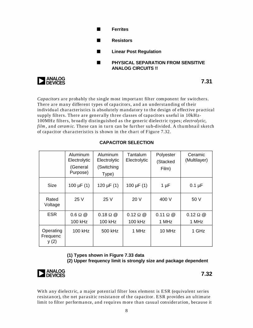
Capacitors are probably the single most important filter component for switchers.There are many different types of capacitors, and an understanding of theirindividual characteristics is absolutely mandatory to the design of effective practicalsupply filters. There are generally three classes of capacitors useful in 10kHz-100MHz filters, broadly distinguished as the generic dielectric types; electrolytic,film, and ceramic. These can in turn can be further sub-divided. A thumbnail sketchof capacitor characteristics is shown in the chart of Figure 7.32.
CAPACITOR SELECTION
AluminumElectrolytic
(GeneralPurpose)
AluminumElectrolytic
(Switching
Type)
TantalumElectrolytic
Polyester
(Stacked
Film)
Ceramic(Multilayer)
Size 100 µF (1) 120 µF (1) 100 µF (1) 1 µF 0.1 µF
RatedVoltage
25 V 25 V 20 V 400 V 50 V
ESR 0.6 Ω @
100 kHz
0.18 Ω @
100 kHz
0.12 Ω @
100 kHz
0.11 Ω @
1 MHz
0.12 Ω @
1 MHz
OperatingFrequenc
y (2)
≅ 100 kHz ≅ 500 kHz ≅ 1 MHz ≅ 10 MHz ≅ 1 GHz
(1) Types shown in Figure 7.33 data(2) Upper frequency limit is strongly size and package dependent
a 7.32
With any dielectric, a major potential filter loss element is ESR (equivalent seriesresistance), the net parasitic resistance of the capacitor. ESR provides an ultimatelimit to filter performance, and requires more than casual consideration, because it
9
can vary both with frequency and temperature in some types. Another capacitor losselement is ESL (equivalent series inductance). ESL determines the frequency wherethe net impedance characteristic switches from capacitive to inductive. This variesfrom as low as 10kHz in some electrolytics to as high as 100MHz or more in chipceramic types. Both ESR and ESL are minimized when a leadless package is used.All capacitor types mentioned are available in surface mount packages, preferablefor high speed uses.
The electrolytic family provides an excellent, cost-effective low-frequency filtercomponent, because of the wide range of values, a high capacitance-to-volume ratio,and a broad range of working voltages. It includes general purpose aluminumelectrolytic types, available in working voltages from below 10V up to about 500V,and in size from 1 to several thousand µF (with proportional case sizes). Allelectrolytic capacitors are polarized, and thus cannot withstand more than a volt orso of reverse bias without damage. They also have relatively high leakage currents(up to tens of µA, and strongly dependent upon design specifics).
A subset of the general electrolytic family includes tantalum types, generally limitedto voltages of 100V or less, with capacitance of 500µF or less[Reference 3]. In a givensize, tantalums exhibit a higher capacitance-to-volume ratios than do generalpurpose electrolytics, and have both a higher frequency range and lower ESR. Theyare generally more expensive than standard electrolytics, and must be carefullyapplied with respect to surge and ripple currents.
A subset of aluminum electrolytic capacitors is the switching type, designed forhandling high pulse currents at frequencies up to several hundred kHz with lowlosses [Reference 4]. This capacitor type competes directly with tantalums in highfrequency filtering applications, with the advantage of a broader range of values.
A more specialized high performance aluminum electrolytic capacitor type uses anorganic semiconductor electrolyte [Reference 5]. The OS-CON capacitors featureappreciably lower ESR and higher frequency range than do other electrolytic types,with an additional feature of low low-temperature ESR degradation.
Film capacitors are available in very broad value ranges and an array of dielectrics,including polyester, polycarbonate, polypropylene, and polystyrene. Because of thelow dielectric constant of these films, their volumetric efficiency is quite low, and a10µF/50V polyester capacitor (for example) is actually a handful. Metalized (asopposed to foil) electrodes does help to reduce size, but even the highest dielectricconstant units among film types (polyester, polycarbonate) are still larger than anyelectrolytic, even using the thinnest films with the lowest voltage ratings (50V).Where film types excel is in their low dielectric losses, a factor which may notnecessarily be a practical advantage for filtering switchers. For example, ESR infilm capacitors can be as low as 10mΩ or less, and the behavior of films generally isvery high in terms of Q. In fact, this can cause problems of spurious resonance infilters, requiring damping components.
Typically using a wound layer-type construction, film capacitors can be inductive,which can limit their effectiveness for high frequency filtering. Obviously, only non-inductively made film caps are useful for switching regulator filters. One specificstyle which is non-inductive is the stacked-film type, where the capacitor plates arecut as small overlapping linear sheet sections from a much larger wound drum of
10
dielectric/plate material. This technique offers the low inductance attractiveness of aplate sheet style capacitor with conventional leads [see References 4, 5, 6].Obviously, minimal lead length should be used for best high frequency effectiveness.Very high current polycarbonate film types are also available, specifically designedfor switching power supplies, with a variety of low inductance terminations tominimize ESL [Reference 7].
Dependent upon their electrical and physical size, film capacitors can be useful atfrequencies to well above 10MHz. At the highest frequencies, only stacked film typesshould be considered. Some manufacturers are now supplying film types in leadlesssurface mount packages, which eliminates the lead length inductance.
Ceramic is often the capacitor material of choice above a few MHz, due to itscompact size, low loss, and availability up to several µF in the high-K dielectricformulations (X7R and Z5U), at voltage ratings up to 200V [see ceramic families ofReference 3]. NP0 (also called COG) types use a lower dielectric constantformulation, and have nominally zero TC, plus a low voltage coefficient (unlike theless stable high-K types). NP0 types are limited to values of 0.1µF or less, with0.01µF representing a more practical upper limit.
Multilayer ceramic “chip caps” are very popular for bypassing/ filtering at 10MHz ormore, simply because their very low inductance design allows near optimum RFbypassing. For smaller values, ceramic chip caps have an operating frequency rangeto 1GHz. For high frequency applications, a useful selection can be ensured byselecting a value which has a self-resonant frequency above the highest frequency ofinterest.
All capacitors have some finite ESR. In some cases, the ESR may actually be helpfulin reducing resonance peaks in filters, by supplying “free” damping. For example, inmost electrolytic types, a nominally flat broad series resonance region can be notedin an impedance vs. frequency plot. This occurs where |Z| falls to a minimum level,nominally equal to the capacitor’s ESR at that frequency. This low Q resonance cangenerally be noted to cover a relatively wide frequency range of several octaves.Contrasted to the very high Q sharp resonances of film and ceramic caps, the low Qbehavior of electrolytics can be useful in controlling resonant peaks.
In most electrolytic capacitors, ESR degrades noticeably at low temperature, by asmuch as a factor of 4-6 times at –55°C vs. the room temperature value. For circuitswhere ESR is critical to performance, this can lead to problems. Some specificelectrolytic types do address this problem, for example within the HFQ switchingtypes, the –10°C ESR at 100kHz is no more than 2× that at room temperature. TheOSCON electrolytics have a ESR vs. temperature characteristic which is relativelyflat.
Figure 7.33 illustrates the high frequency impedance characteristics of a number ofelectrolytic capacitor types, using nominal 100µF/20V samples. In these plots, theimpedance, |Z|, vs. frequency over the 20Hz-200kHz range is displayed using ahigh resolution 4-terminal setup [Reference 8]. Shown in this display areperformance samples for a 100µF/25V general purpose aluminum unit (top curve @right), a 120µF/25V HFQ unit (next curve down @ right), a 100µF/20V tantalumbead type (next curve down @ right), and a 100µF/20V OS-CON unit (lowest curve @right). While the HFQ and tantalum samples are close in 100kHz impedance, the
11
general purpose unit is about 4 times worse. The OS-CON unit is nearly an order ofmagnitude lower in 100kHz impedance than the tantalum and switching electrolytictypes.
IMPEDANCE Z(ΩΩ)) VS. FREQUENCY FOR 100µµFELECTROLYTIC CAPACITORS (AC CURRENT = 50mA RMS)
7.33a
100
10
1
0.1
10m
1m
Z(ΩΩ)
FREQUENCY (Hz)20 100 1k 10k 100k 200k
"HFQ" 120µF, 25V
GEN. PURPOSE AL100µF, 25V
TANTALUM BEAD100µF, 20V
OS-CON AL100µF, 20V
As noted, all real capacitors have parasitic elements which limit their performance.The equivalent electrical network representing a real capacitor models both ESRand ESL as well as the basic capacitance, plus some shunt resistance. In such apractical capacitor, at low frequencies the net impedance is almost purely capacitive(noted in Figure 7.33 by the 100Hz impedance). At intermediate frequencies, the netimpedance is determined by ESR, for example about 0.12Ω to 0.4Ω at 125kHz, forseveral types. Above about 1MHz these capacitor types become inductive, withimpedance dominated by the effect of ESL (not shown). All electrolytics will displayimpedance curves similar in general shape. The minimum impedance will vary withthe ESR, and the inductive region will vary with ESL (which in turn is stronglyeffected by package style).
Regarding inductors, Ferrites (non-conductive ceramics manufactured from theoxides of nickel, zinc, manganese, or other compounds) are extremely useful inpower supply filters [Reference 9]. At low frequencies (<100kHz), ferrites areinductive; thus they are useful in low-pass LC filters. Above 100kHz, ferrites becomeresistive, an important characteristic in high-frequency filter designs. Ferriteimpedance is a function of material, operating frequency range, DC bias current,number of turns, size, shape, and temperature. Figure 7.34 summarize a numberferrite characteristics.
CHARACTERISTICS OF FERRITES
nn Good for frequencies above 25kHz
12
nn Many sizes and shapes available includingleaded "resistor style"
nn Ferrite impedance at high frequencies isprimarily resistive -- Ideal for HF filtering
nn Low DC loss: Resistance of wire passing throughferrite is very low
nn High saturation current
nn Low cost
a 7.34
Several ferrite manufacturers offer a wide selection of ferrite materials from whichto choose, as well as a variety of packaging styles for the finished network (seeReferences 10 and 11). A simple form is the bead of ferrite material, a cylinder of theferrite which is simply slipped over the power supply lead to the decoupled stage.Alternately, the leaded ferrite bead is the same bead, pre-mounted on a length ofwire and used as a component (see Reference 11). More complex beads offer multipleholes through the cylinder for increased decoupling, plus other variations. Surfacemount beads are also available.
PSpice ferrite models for Fair-Rite materials are available, and allow ferriteimpedance to be estimated [see Reference 12]. These models have been designed tomatch measured impedances rather than theoretical impedances.
A ferrite’s impedance is dependent upon a number of inter-dependent variables, andis difficult to quantify analytically, thus selecting the proper ferrite is notstraightforward. However, knowing the following system characteristics will makeselection easier. First, determine the frequency range of the noise to be filtered.Second, the expected temperature range of the filter should be known, as ferriteimpedance varies with temperature. Third, the DC current flowing through theferrite must be known, to ensure that the ferrite does not saturate. Although modelsand other analytical tools may prove useful, the general guidelines given above,coupled with some experimentation with the actual filter connected to the supplyoutput under system load conditions, should lead to a proper ferrite selection.
CHOOSING THE RIGHT FERRITE DEPENDS ON
nn Source of Interference
nn Interference Frequency Range
nn Impedance Required at Interference Frequency
nn Environmental Conditions:
Temperature, AC and DC Field Strength,
13
Size / Space Available
nn Don't fail to Test the Design -------
EXPERIMENT! EXPERIMENT!
a 7.35
Using proper component selection, low and high frequency band filters can bedesigned to smooth a noisy switcher’s DC output so as to produce an analog ready5V supply. It is most practical to do this over two (and sometimes more) stages, eachstage optimized for a range of frequencies. A basic stage can be used to carry all ofthe DC load current, and filter noise by 60dB or more up to a 1-10MHz range. Thislarger filter is used as a card entry filter providing broadband filtering for all powerentering a PC card. Smaller, more simple local filter stages are also used to providehigher frequency decoupling right at the power pins of individual stages.
Figure 7.36 illustrates a card entry filter suitable for use with switching supplies.With a low rolloff point of 1.5kHz and mV level DC errors, it is effective for a widevariety of filter applications just as shown. This filter is a single stage LC low-passfilter covering the 1kHz to 1MHz range, using carefully chosen parts. Because ofcomponent losses, it begins to lose effectiveness above a few MHz, but is still able toachieve an attenuation approaching 60dB at 1MHz.
"CARD-ENTRY" SWITCHING SUPPLY FILTER
7.36a
C1100µµF,20V
TANTALUM
R11ΩΩ
5V INPUTFROM NOISYSWITCHING
SUPPLY OR DCTO DC
CONVERTER
C21µµFCERAMIC
L1
100µµH
+ +
- -
OUTPUT TO300mA LOAD
ANALOG STAGE+
The key to low DC losses is the use of input choke, L1, a ferrite-core unit selected fora low DC resistance (DCR) of <0.25Ω at the 100µH inductance (either an axial lead

14
type 5250 or a radial style 6000-101K choke should give comparable results)[Reference 13]. These chokes have low inductance shift with a 300mA load current,and the low DCR allows the 300mA to be passed with no more than 75mV of DCerror. Alternately, resistive filtering might be used in place of L1, but a basictradeoff here is that load current capacity will be compromised for comparable DCerrors. C1, a 100µF/20V tantalum type, provides the bulk of the capacitive filtering,shunted by a 1µF multilayer ceramic.
Figure 7.37 shows the frequency response of this filter in terms of SPICE simulationand lab measurements, with good agreement between the simulation and themeasurements below 1MHz.
OUTPUT RESPONSE OF "CARD-ENTRY" FILTERLAB VS. SIMULATION
7.37a
0
-20
-40
-60
-80
-100
Z(ΩΩ)
FREQUENCY (Hz)10 100 1.0k 10k 100k 1.0M 10M 100M
= SPICE SIMULATION= LAB RESULTSX
X X XX
X
X
X
X
X
X
X
X
X
This type of filter does have some potential pitfalls, and one of them is the control ofresonances. If the LCR circuit formed does not have sufficiently high resistance atthe resonant frequency, amplitude peaking will result. This peaking can beminimized with resistance at two locations: in series with L1, or in series withC1+C2. Obviously, limited resistance is usable in series with L1, as this increasesthe DC errors.
In the filter, R1 is a damping resistor, used to control resonant peaks, and it shouldnot be eliminated. A 1Ω value provides a slightly underdamped response, withpeaking on the order of 1dB. Alternately, 1.5Ω can be used for less peaking, with atradeoff of less attenuation below 1MHz. Note that for wide temperature rangeapplications, all temperature sensitive filter components will need consideration.
15
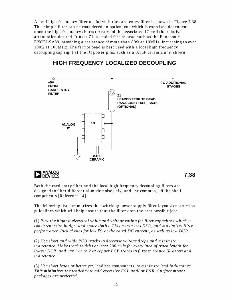
A local high frequency filter useful with the card entry filter is shown in Figure 7.38.This simple filter can be considered an option, one which is exercised dependentupon the high frequency characteristics of the associated IC and the relativeattenuation desired. It uses Z1, a leaded ferrite bead such as the PanasonicEXCELSA39, providing a resistance of more than 80Ω at 10MHz, increasing to over100Ω at 100MHz. The ferrite bead is best used with a local high frequencydecoupling cap right at the IC power pins, such as a 0.1µF ceramic unit shown.
HIGH FREQUENCY LOCALIZED DECOUPLING
7.38a
Z1LEADED FERRITE BEADPANASONIC EXCELSA39(OPTIONAL)
+5VFROMCARD-ENTRYFILTER
ANALOGIC
U1
0.1µµFCERAMIC
TO ADDITIONALSTAGES
U1
Both the card entry filter and the local high frequency decoupling filters aredesigned to filter differential-mode noise only, and use common, off the shelfcomponents [Reference 14].
The following list summarizes the switching power supply filter layout/constructionguidelines which will help ensure that the filter does the best possible job:
(1) Pick the highest electrical value and voltage rating for filter capacitors which isconsistent with budget and space limits. This minimizes ESR, and maximizes filterperformance. Pick chokes for low ∆L at the rated DC current, as well as low DCR.
(2) Use short and wide PCB tracks to decrease voltage drops and minimizeinductance. Make track widths at least 200 mils for every inch of track length forlowest DCR, and use 1 oz or 2 oz copper PCB traces to further reduce IR drops andinductance.
(3) Use short leads or better yet, leadless components, to minimize lead inductance.This minimizes the tendency to add excessive ESL and/or ESR. Surface mountpackages are preferred.
16
(4) Use a large-area ground plane for minimum impedance.
(5) Know what your components do over frequency, current and temperaturevariations! Make use of vendor component models for the simulation of prototypedesigns, and make sure that lab measurements correspond reasonably with thesimulation. While simulation is not absolutely necessary, it does instill confidence ina design when correlation is achieved(see Reference 15).
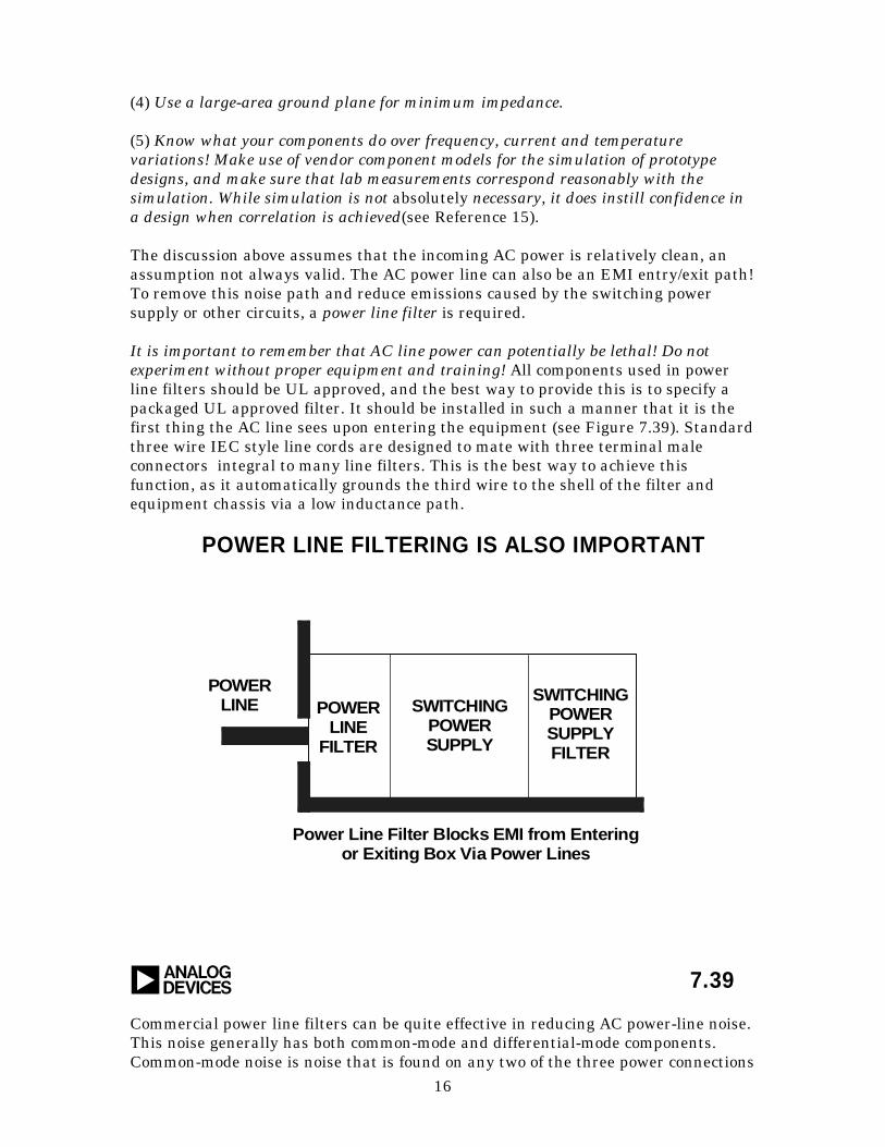
The discussion above assumes that the incoming AC power is relatively clean, anassumption not always valid. The AC power line can also be an EMI entry/exit path!To remove this noise path and reduce emissions caused by the switching powersupply or other circuits, a power line filter is required.
It is important to remember that AC line power can potentially be lethal! Do notexperiment without proper equipment and training! All components used in powerline filters should be UL approved, and the best way to provide this is to specify apackaged UL approved filter. It should be installed in such a manner that it is thefirst thing the AC line sees upon entering the equipment (see Figure 7.39). Standardthree wire IEC style line cords are designed to mate with three terminal maleconnectors integral to many line filters. This is the best way to achieve thisfunction, as it automatically grounds the third wire to the shell of the filter andequipment chassis via a low inductance path.
POWER LINE FILTERING IS ALSO IMPORTANT
7.39a
POWERLINE POWER
LINEFILTER
SWITCHINGPOWERSUPPLY
SWITCHINGPOWERSUPPLYFILTER
Power Line Filter Blocks EMI from Enteringor Exiting Box Via Power Lines
Commercial power line filters can be quite effective in reducing AC power-line noise.This noise generally has both common-mode and differential-mode components.Common-mode noise is noise that is found on any two of the three power connections

17
(black, white, or green) with the same amplitude and polarity. In contrast,differential-mode noise is noise found only between two lines. By design, mostcommercially available filters address both noise modes (see Reference 16).
18
REFERENCES: NOISE REDUCTION AND FILTERING
1. EMC Design Workshop Notes, Kimmel-Gerke Associates, Ltd.,St. Paul, MN. 55108, (612) 330-3728.
2. Walt Jung, Dick Marsh, Picking Capacitors, Parts 1 & 2, Audio,February, March, 1980.
3. Tantalum Electrolytic and Ceramic Capacitor Families, KemetElectronics, Box 5928, Greenville, SC, 29606, (803) 963-6300.
4. Type HFQ Aluminum Electrolytic Capacitor and type V StackedPolyester Film Capacitor, Panasonic, 2 Panasonic Way, Secaucus,NJ, 07094, (201) 348-7000.
5. OS-CON Aluminum Electrolytic Capacitor 93/94 Technical Book,Sanyo, 3333 Sanyo Road, Forrest City, AK, 72335, (501) 633-6634.
6. Ian Clelland, Metalized Polyester Film Capacitor Fills High FrequencySwitcher Needs, PCIM, June 1992.
7. Type 5MC Metallized Polycarbonate Capacitor, Electronic Concepts, Inc.,Box 1278, Eatontown, NJ, 07724, (908) 542-7880.
8. Walt Jung, Regulators for High-Performance Audio, Parts 1 and 2,The Audio Amateur, issues 1 and 2, 1995.
9. Henry Ott, Noise Reduction Techniques in Electronic Systems,2d Ed., 1988, Wiley.
10. Fair-Rite Linear Ferrites Catalog, Fair-Rite Products, Box J, Wallkill,NY, 12886, (914) 895-2055.
11. Type EXCEL leaded ferrite bead EMI filter, and type EXC L leadlessferrite bead, Panasonic, 2 Panasonic Way, Secaucus, NJ, 07094,(201) 348-7000.
12. Steve Hageman, Use Ferrite Bead Models to Analyze EMI Suppression,The Design Center Source, MicroSim Newsletter, January, 1995.
13. Type 5250 and 6000-101K chokes, J. W. Miller, 306 E. Alondra Blvd.,Gardena, CA, 90247, (310) 515-1720.
14. DIGI-KEY, PO Box 677, Thief River Falls, MN, 56701-0677,(800) 344-4539.
15. Tantalum Electrolytic Capacitor SPICE Models, Kemet Electronics,Box 5928, Greenville, SC, 29606, (803) 963-6300.
16. Eichhoff Electronics, Inc., 205 Hallene Road, Warwick, RI., 02886,(401) 738-1440.
19
POWER SUPPLY REGULATION/CONDITIONING
Walt Jung
Many analog circuits require stable regulated voltages relatively close in potentialto an unregulated source. An example would be a linear post regulator for aswitching power supply, where voltage loss (dropout) is critical. This low dropouttype of regulator is readily implemented with a rail-rail output op amp. The wideoutput swing and low saturation voltage enables outputs to come within a fraction ofa volt of the source for medium current (<30mA) loads, such as referenceapplications. For higher output currents, the rail-rail voltage swing feature allowsdirect drive to low saturation voltage pass devices, such as power PNPs or P-channelMOSFETs. Op amps working from 3V up with the rail-rail features are mostsuitable here, providing power economy and maximum flexibility.
LOW DROPOUT REFERENCES
Basic references
Among the many problems in making stable DC voltage references work from 5Vand lower supplies are quiescent power consumption, overall efficiency, the ability tooperate down to 3V, low input/output (dropout) capability, and minimum noiseoutput. Because low voltage supplies can't support zeners of ≅6V, low voltage refer-ences must necessarily be bandgap based-- a basic ≅1.2V potential. With low voltagesystems, power conservation can be a critical issue with references, as can outputDC precision.
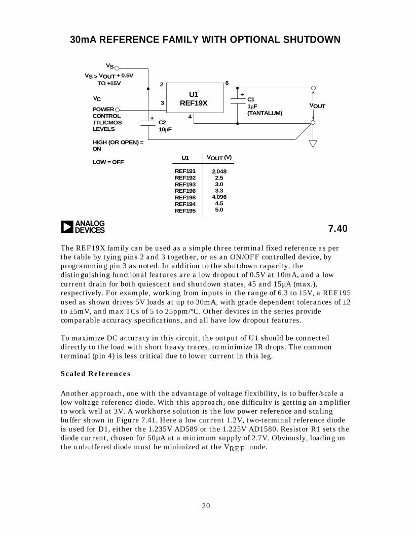
For many applications, simple one-package fixed (or variable) voltage referenceswith minimal external circuitry and high accuracy are attractive. Two uniquefeatures of the three terminal REF19X bandgap reference family are low power, andshutdown capability. The series allows fixed outputs from 2.048-5V to be controlledbetween ON and OFF, via a TTL/CMOS power control input. It provides precisionreference quality for those popular voltages shown in Figure 7.40.
20
30mA REFERENCE FAMILY WITH OPTIONAL SHUTDOWN
7.40a
VOUTC11µµF(TANTALUM)
VS > VOUT + 0.5VTO +15V
VOUT (V)
2.0482.53.03.3
4.0964.55.0
U1REF19X
6
+
4
2
3
VS
+C210µµF
VC
POWERCONTROLTTL/CMOSLEVELS
HIGH (OR OPEN) =ON
LOW = OFFU1
REF191REF192REF193REF196REF198REF194REF195
The REF19X family can be used as a simple three terminal fixed reference as perthe table by tying pins 2 and 3 together, or as an ON/OFF controlled device, byprogramming pin 3 as noted. In addition to the shutdown capacity, thedistinguishing functional features are a low dropout of 0.5V at 10mA, and a lowcurrent drain for both quiescent and shutdown states, 45 and 15µA (max.),respectively. For example, working from inputs in the range of 6.3 to 15V, a REF195used as shown drives 5V loads at up to 30mA, with grade dependent tolerances of ±2to ±5mV, and max TCs of 5 to 25ppm/°C. Other devices in the series providecomparable accuracy specifications, and all have low dropout features.
To maximize DC accuracy in this circuit, the output of U1 should be connecteddirectly to the load with short heavy traces, to minimize IR drops. The commonterminal (pin 4) is less critical due to lower current in this leg.
Scaled References
Another approach, one with the advantage of voltage flexibility, is to buffer/scale alow voltage reference diode. With this approach, one difficulty is getting an amplifierto work well at 3V. A workhorse solution is the low power reference and scalingbuffer shown in Figure 7.41. Here a low current 1.2V, two-terminal reference diodeis used for D1, either the 1.235V AD589 or the 1.225V AD1580. Resistor R1 sets thediode current, chosen for 50µA at a minimum supply of 2.7V. Obviously, loading onthe unbuffered diode must be minimized at the VREF node.
21
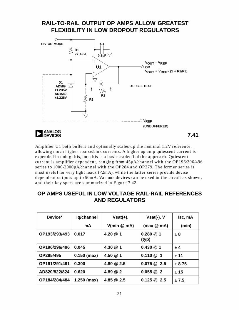
RAIL-TO-RAIL OUTPUT OP AMPS ALLOW GREATESTFLEXIBILITY IN LOW DROPOUT REGULATORS
7.41
C1
0.1µµF
R3R2
D1AD589
+1.235VAD1580+1.225V
U1
+3V OR MORE
VREF(UNBUFFERED)
VOUT = VREFORVOUT = VREF× × (1 + R2/R3)
U1: SEE TEXT
R127.4kΩΩ
+
-
a
Amplifier U1 both buffers and optionally scales up the nominal 1.2V reference,allowing much higher source/sink currents. A higher op amp quiescent current isexpended in doing this, but this is a basic tradeoff of the approach. Quiescentcurrent is amplifier dependent, ranging from 45µA/channel with the OP196/296/496series to 1000-2000µA/channel with the OP284 and OP279. The former series ismost useful for very light loads (<2mA), while the latter series provide devicedependent outputs up to 50mA. Various devices can be used in the circuit as shown,and their key specs are summarized in Figure 7.42.
OP AMPS USEFUL IN LOW VOLTAGE RAIL-RAIL REFERENCESAND REGULATORS
Device* Iq/channel
mA
Vsat(+),
V(min @ mA)
Vsat(-), V
(max @ mA)
Isc, mA
(min)
OP193/293/493 0.017 4.20 @ 1 0.280 @ 1(typ)
±± 8
OP196/296/496 0.045 4.30 @ 1 0.430 @ 1 ±± 4
OP295/495 0.150 (max) 4.50 @ 1 0.110 @ 1 ±± 11
OP191/291/491 0.300 4.80 @ 2.5 0.075 @ 2.5 ±± 8.75
AD820/822/824 0.620 4.89 @ 2 0.055 @ 2 ±± 15
OP184/284/484 1.250 (max) 4.85 @ 2.5 0.125 @ 2.5 ±± 7.5
22
OP279 2.000 4.80 @ 10 0.075 @ 10 ±± 45
*Typical device specifications @ Vs = +5V, TA = 25°°C, unless otherwise noted.
a 7.42
In Figure 7.41, without gain scaling resistors R2-R3, VOUT is simply equal to VREF.With the scaling resistors, VOUT can be set anywhere between VREF and thepositive rail, due to the op amp’s rail-rail output swing. Also, this buffered referenceis inherently low dropout, allowing a +4.5V reference output on a +5V supply, forexample. The general expression for VOUT is shown in the figure, where VREF isthe reference voltage.
Amplifier standby current can be further reduced below 20µA, if an amplifier fromthe OP193/293/493 series is used. This will be at the expense of current drive andpositive rail saturation, but does provide the lowest possible quiescent current ifnecessary. All devices in Figure 7.42 operate from voltages down to 3V (except theOP279, which operates at 5V).
Low Dropout Regulators
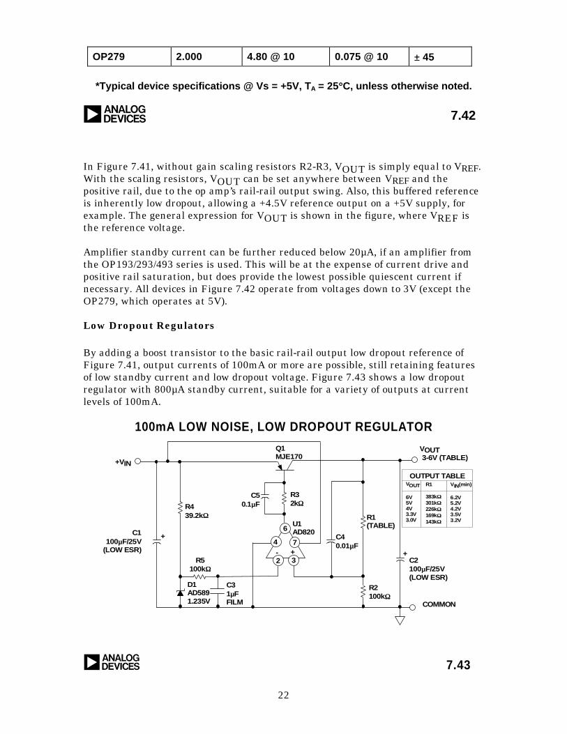
By adding a boost transistor to the basic rail-rail output low dropout reference ofFigure 7.41, output currents of 100mA or more are possible, still retaining featuresof low standby current and low dropout voltage. Figure 7.43 shows a low dropoutregulator with 800µA standby current, suitable for a variety of outputs at currentlevels of 100mA.
100mA LOW NOISE, LOW DROPOUT REGULATOR
7.43a
VOUT
VOUT
6V5V4V3.3V3.0V
+
+VIN
+C1100µµF/25V
(LOW ESR)
R439.2kΩΩ
C50.1µµF
R32kΩΩ
R1(TABLE)
Q1MJE170
U1AD820
C40.01µµF
COMMON
C2100µµF/25V(LOW ESR)
3-6V (TABLE)
C31µµFFILM
R5100kΩΩ
D1AD5891.235V
R2100kΩΩ
+-
6
4 7
2 3
R1
383kΩΩ301kΩΩ226kΩΩ169kΩΩ143kΩΩ
VIN(min)
6.2V5.2V4.2V3.5V3.2V
OUTPUT TABLE
23
The 100mA output is achieved with a controlled gain bipolar power transistor forpass device Q1, an MJE170. Maximum output current control is provided bylimiting base drive to Q1 via series resistor R3. This limits the base current to about2mA, so the max HFE of Q1 then allows no more than 500mA. This limits Q1’s shortcircuit power dissipation to safe levels.
Overall, the circuit operates as a follower with gain, as was true in the case ofFigure 7.41, so VOUT has a similar output expression. The circuit is adapted fordifferent voltages simply by programming R1 via the table. Dropout with a 100mAload is about 200mV, thus a 5V output is maintained for inputs above 5.2V (seetable), and VOUT levels down to 3V are possible. Step load response of this circuit isquite good, and transient error is only a few mVp-p for a 30-100mA load change.This is achieved with low ESR switching type capacitors at C1-C2, but the circuitalso works with conventional electrolytics (with higher transient errors).
If desired, lowest output noise with the AD820 is reached by including the optionalreference noise filter, R5-C3. Lower current op amps can also be used for lowerstandby current, but with larger transient errors due to reduced bandwidth.
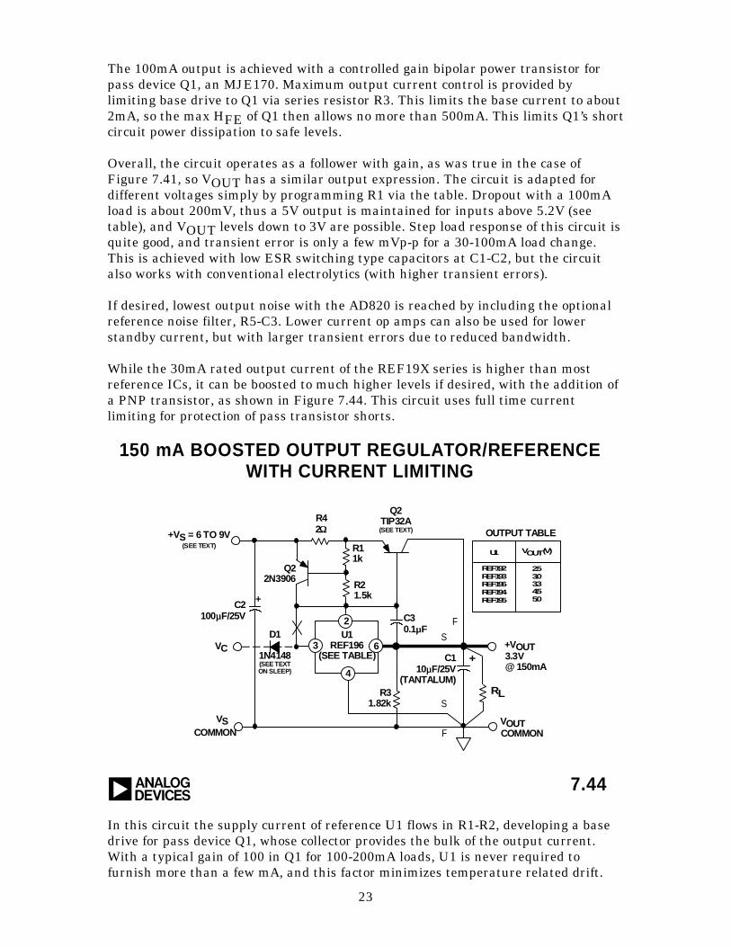
While the 30mA rated output current of the REF19X series is higher than mostreference ICs, it can be boosted to much higher levels if desired, with the addition ofa PNP transistor, as shown in Figure 7.44. This circuit uses full time currentlimiting for protection of pass transistor shorts.
150 mA BOOSTED OUTPUT REGULATOR/REFERENCEWITH CURRENT LIMITING
7.44a
U1
REF192REF193REF196REF194REF195
VOUT (V)
2.53.03.34.55.0
R11k
VOUT
+VS = 6 TO 9V(SEE TEXT)
+C2
100µµF/25V
Q22N3906
COMMON
C30.1µµF
R42ΩΩ
RL
COMMONVS
U1REF196
(SEE TABLE)VC
C110µµF/25V
(TANTALUM)4
3 6
2
+
R21.5k
Q2TIP32A(SEE TEXT)
D1
1N4148(SEE TEXTON SLEEP)
R31.82k
F
S
S
F
+VOUT3.3V@ 150mA
OUTPUT TABLE
In this circuit the supply current of reference U1 flows in R1-R2, developing a basedrive for pass device Q1, whose collector provides the bulk of the output current.With a typical gain of 100 in Q1 for 100-200mA loads, U1 is never required tofurnish more than a few mA, and this factor minimizes temperature related drift.
24
Short circuit protection is provided by Q2, which clamps drive to Q1 at about 300mAof load current. With separation of control/power functions, DC stability is optimum,allowing best advantage of premium grade REF19X devices for U1. Of course, loadmanagement should still be exercised. A short, heavy, low resistance conductorshould be used from U1-6 to the VOUT sense point “S”, where the collector of Q1connects to the load.
Because of the current limiting, dropout voltage is raised about 1.1V over that of theREF19X devices. However, overall dropout typically is still low enough to allowoperation of a 5 to 3.3V regulator/reference using the 3.3V REF-196 for U1, with aVs of 4.5V and a load current of 150mA.
The heat sink requirements of Q1 depend upon the maximum power. With Vs = 5Vand a 300mA current limit, the worst case dissipation of Q1 is 1.5W, less than theTO-220 package 2W limit. If TO-39 or TO-5 packaged devices such as the 2N4033are used, the current limit should be reduced to keep maximum dissipation belowthe package rating, by raising R4. A tantalum output capacitor is used at C1 for itslow ESR, and the higher value is required for stability. Capacitor C2 provides inputbypassing, and can be an ordinary electrolytic.
Shutdown control of the booster stage is shown as an option, and when used, somecautions are in order. To enable shutdown control, the connection to U1-2 and U1-3is broken at “X”, and diode D1 allows a CMOS control source to drive U1-3 forON/OFF control. Startup from shutdown is not as clean under heavy load as it iswith the basic REF19X series stand-alone, and can require several millisecondsunder load. Nevertheless, it is still effective, and can fully control 150mA loads.When shutdown control is used, heavy capacitive loads should be minimized.
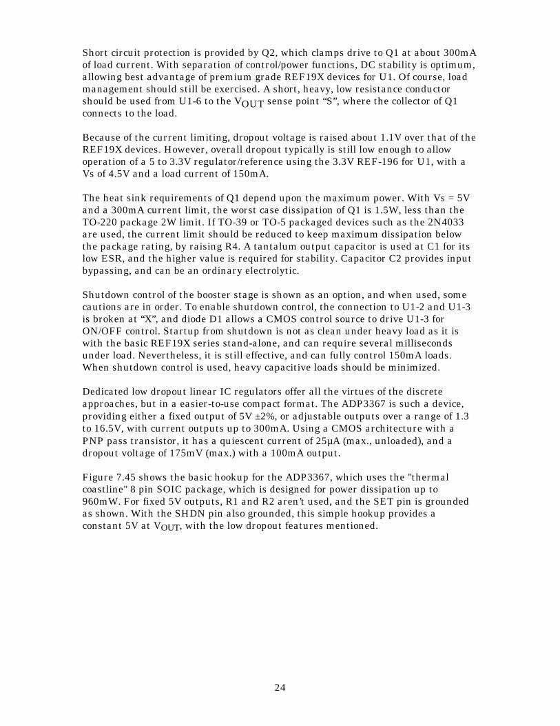
Dedicated low dropout linear IC regulators offer all the virtues of the discreteapproaches, but in a easier-to-use compact format. The ADP3367 is such a device,providing either a fixed output of 5V ±2%, or adjustable outputs over a range of 1.3to 16.5V, with current outputs up to 300mA. Using a CMOS architecture with aPNP pass transistor, it has a quiescent current of 25µA (max., unloaded), and adropout voltage of 175mV (max.) with a 100mA output.
Figure 7.45 shows the basic hookup for the ADP3367, which uses the "thermalcoastline" 8 pin SOIC package, which is designed for power dissipation up to960mW. For fixed 5V outputs, R1 and R2 aren’t used, and the SET pin is groundedas shown. With the SHDN pin also grounded, this simple hookup provides aconstant 5V at VOUT, with the low dropout features mentioned.
25
R1
WITH R1, R2:
VOUT = VREF ( )WHERE VREF = +1.255V,
VOUT = +3.3V (VALUES SHOWN)
a
300mA LOW DROPOUT FIXED/VARIABLEREGULATOR WITH OPTIONAL SHUTDOWN
7.45
R2
R2162kΩΩ
VIN VOUT
C1
0.1µµF
C2
10µµF
R1100kΩΩVSHDN
IN OUT
SETSHDN
+5.15VTO
+16.5V
+5V
*
*
GND
+
1 +
ADP3367
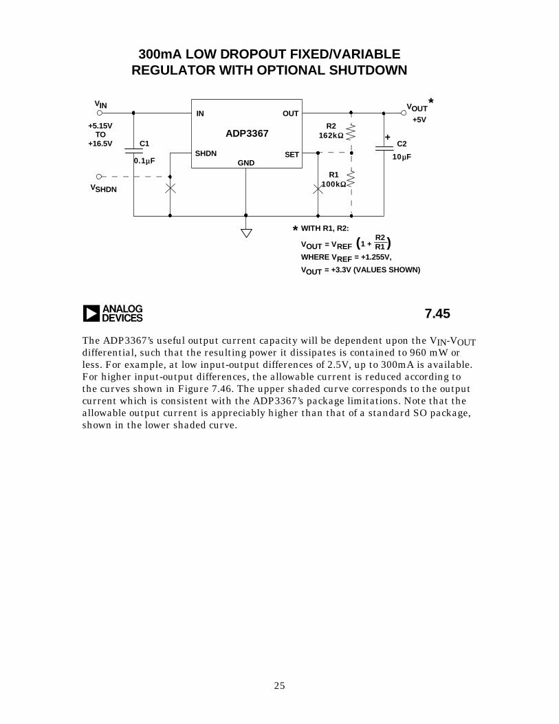
The ADP3367’s useful output current capacity will be dependent upon the VIN-VOUTdifferential, such that the resulting power it dissipates is contained to 960 mW orless. For example, at low input-output differences of 2.5V, up to 300mA is available.For higher input-output differences, the allowable current is reduced according tothe curves shown in Figure 7.46. The upper shaded curve corresponds to the outputcurrent which is consistent with the ADP3367’s package limitations. Note that theallowable output current is appreciably higher than that of a standard SO package,shown in the lower shaded curve.
26
7.46
ADP3367 LOAD CURRENT VS. INPUT - OUTPUT VOLTAGE
aVINVOUT V
400
200
00 155 10
100
TA = +50°C
300GUARANTEED 300mA
ADP3367DISSIPATION LIMIT
STANDARDSO PACKAGEDISSIPATION LIMIT
LOA
D C
UR
RE
NT
- m
A
The ADP3367 can be placed in a shutdown mode, which reduces the output voltageto zero and drops the standby current to less than 1µA. When implemented,shutdown is accomplished by applying a control voltage of more than 1.5V to VSHDN.Otherwise, this pin should be tied to ground as shown. The SET pin has a dualfunction, and can be used either to select an internal divider (which provides thefixed 5V output), or it can be used with an external divider, R1-R2. When the SETpin is grounded, the internal divider is active, and the 5 V output results. When theSET pin is used with the external divider, VOUT is programmed as:
VOUT VREFR2R1
= ∗ +
1
where VREF is 1.255V, the internal reference voltage of the ADP3367. The divider’sabsolute resistance values are not critical, since the input current at the SET pin islow, typically 10pA. This allows resistances of 100k - 1meg, consistent with theoverall low standby power objectives. The example 1% values shown provide a 3.3Voutput. They can be further increased, if it is desired to lower standby currentconsumption below the ≅12µA resulting with the values shown.
C2, the output capacitor, is a 10µF type, and is required for regulator stability.Larger sizes are permissible, and will help improve transient response. An inputbypass is also recommended, C1.
To achieve the full power capability inherent to the design, the ADP3367 should bemounted on a PCB in such as way that internally-generated heat can flow outwardeasily from the die to the PCB. Large area PCB copper traces should be usedbeneath and around the IC, and mounting should be such that the part is exposed tounrestricted air flow [see Reference 5].

27
28
REFERENCES: POWER SUPPLYREGULATION/CONDITIONING 1. Walt Jung, Build an Ultra-Low-Noise Voltage Reference,
Electronic Design Analog Applications Issue, June 24, 1993.
2. Walt Jung, Getting the Most from IC Voltage References, AnalogDialogue 28-1, 1994.
3. Walt Jung, The Ins and Outs of ‘Green’ Regulators/References ,Electronic Design Analog Applications Issue, June 27, 1994.
4. Walt Jung, Very-Low-Noise 5-V Regulator, Electronic Design,July 25, 1994.
5. “Power Dissipation” Discussions, ADP3367 Data Sheet, Analog Devices.
29
THERMAL MANAGEMENT
Walt Jung
For reliability reasons, modern semiconductor based systems are increasingly calledupon to observe some form of thermal management. All semiconductors have somespecified safe upper limit to junction temperature (TJ), usually on the order of 150°C(but sometimes 175°). Like maximum power supply potentials, maximum junctiontemperature is a worst case limitation which shouldn’t be exceeded. In conservativedesigns, it won’t be approached by less than an ample safety margin. This is acritical point, since the lifetime of all semiconductors is inversely related to theiroperating junction temperature. The cooler semiconductors can be kept duringoperation, the more closely they will approach maximum useful life.
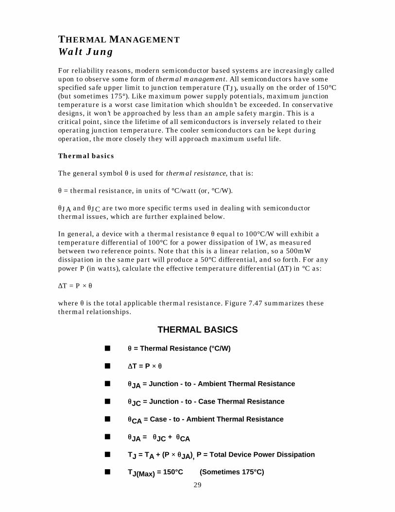
Thermal basics
The general symbol θ is used for thermal resistance, that is:
θ = thermal resistance, in units of °C/watt (or, °C/W).
θJA and θJC are two more specific terms used in dealing with semiconductorthermal issues, which are further explained below.
In general, a device with a thermal resistance θ equal to 100°C/W will exhibit atemperature differential of 100°C for a power dissipation of 1W, as measuredbetween two reference points. Note that this is a linear relation, so a 500mWdissipation in the same part will produce a 50°C differential, and so forth. For anypower P (in watts), calculate the effective temperature differential (∆T) in °C as:
∆T = P × θ
where θ is the total applicable thermal resistance. Figure 7.47 summarizes thesethermal relationships.
THERMAL BASICS
nn θθ = Thermal Resistance (°C/W)
nn ∆∆T = P ×× θθ
nn θθJA = Junction - to - Ambient Thermal Resistance
nn θθJC = Junction - to - Case Thermal Resistance
nn θθCA = Case - to - Ambient Thermal Resistance
nn θθJA = θθJC + θθCA
nn TJ = TA + (P ×× θθJA), P = Total Device Power Dissipation
nn TJ(Max) = 150°C (Sometimes 175°C)
30
a 7.47
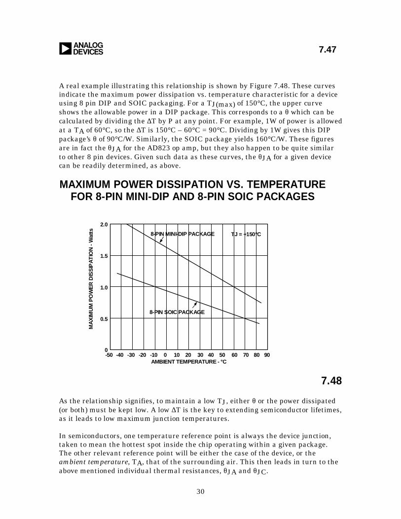
A real example illustrating this relationship is shown by Figure 7.48. These curvesindicate the maximum power dissipation vs. temperature characteristic for a deviceusing 8 pin DIP and SOIC packaging. For a TJ(max) of 150°C, the upper curveshows the allowable power in a DIP package. This corresponds to a θ which can becalculated by dividing the ∆T by P at any point. For example, 1W of power is allowedat a TA of 60°C, so the ∆T is 150°C – 60°C = 90°C. Dividing by 1W gives this DIPpackage’s θ of 90°C/W. Similarly, the SOIC package yields 160°C/W. These figuresare in fact the θJA for the AD823 op amp, but they also happen to be quite similarto other 8 pin devices. Given such data as these curves, the θJA for a given devicecan be readily determined, as above.
7.48
MAXIMUM POWER DISSIPATION VS. TEMPERATUREFOR 8-PIN MINI-DIP AND 8-PIN SOIC PACKAGES
MA
XIM
UM
PO
WE
R D
ISS
IPA
TIO
N -
Wat
ts
AMBIENT TEMPERATURE °C
2.0
1.5
050 9040 30 20 10 0 10 20 30 50 60 70 8040
1.0
0.5
8-PIN MINI-DIP PACKAGE
8-PIN SOIC PACKAGE
TJ = +150°C
As the relationship signifies, to maintain a low TJ, either θ or the power dissipated(or both) must be kept low. A low ∆T is the key to extending semiconductor lifetimes,as it leads to low maximum junction temperatures.
In semiconductors, one temperature reference point is always the device junction,taken to mean the hottest spot inside the chip operating within a given package.The other relevant reference point will be either the case of the device, or theambient temperature, TA, that of the surrounding air. This then leads in turn to theabove mentioned individual thermal resistances, θJA and θJC.
31
Taking the more simple case first, θJA is the thermal resistance of a given devicemeasured between its junction and the ambient air. This thermal resistance is mostoften used with small, relatively low power ICs which do not dissipate seriousamounts of power, that is 1W or less. θJA figures typical of op amps and other smalldevices are on the order of 90-100°C/W for a plastic 8 pin DIP package. It must beunderstood that thermal resistances are highly package dependent, as differentmaterials have differing degrees of thermal conductivity. As a general rule of thumb,thermal resistance for the conductors within packaging materials is closelyanalogous to electrical resistances, that is copper is the best, followed by aluminum,steel, and so on. Thus copper lead frame packages offer the highest performance(lowest θ).
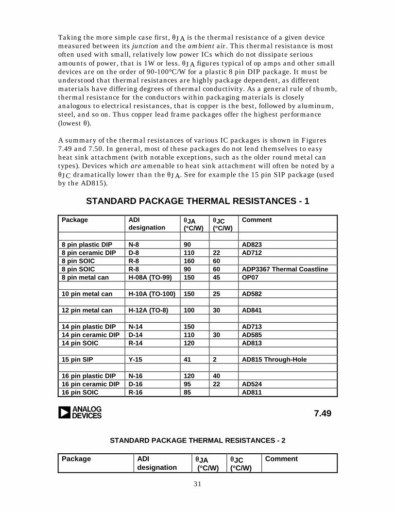
A summary of the thermal resistances of various IC packages is shown in Figures7.49 and 7.50. In general, most of these packages do not lend themselves to easyheat sink attachment (with notable exceptions, such as the older round metal cantypes). Devices which are amenable to heat sink attachment will often be noted by aθJC dramatically lower than the θJA. See for example the 15 pin SIP package (usedby the AD815).
STANDARD PACKAGE THERMAL RESISTANCES - 1
Package ADIdesignation
θθJA(°°C/W)
θθJC(°°C/W)
Comment
8 pin plastic DIP N-8 90 AD8238 pin ceramic DIP D-8 110 22 AD7128 pin SOIC R-8 160 608 pin SOIC R-8 90 60 ADP3367 Thermal Coastline8 pin metal can H-08A (TO-99) 150 45 OP07
10 pin metal can H-10A (TO-100) 150 25 AD582
12 pin metal can H-12A (TO-8) 100 30 AD841
14 pin plastic DIP N-14 150 AD71314 pin ceramic DIP D-14 110 30 AD58514 pin SOIC R-14 120 AD813
15 pin SIP Y-15 41 2 AD815 Through-Hole
16 pin plastic DIP N-16 120 4016 pin ceramic DIP D-16 95 22 AD52416 pin SOIC R-16 85 AD811
a 7.49
STANDARD PACKAGE THERMAL RESISTANCES - 2
Package ADIdesignation
θθJA (°°C/W)
θθJC(°°C/W)
Comment
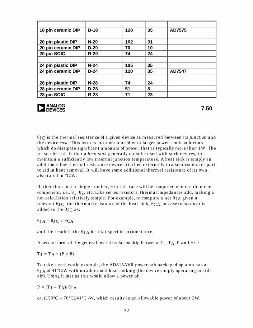
32
18 pin ceramic DIP D-18 120 35 AD7575
20 pin plastic DIP N-20 102 3120 pin ceramic DIP D-20 70 1020 pin SOIC R-20 74 24
24 pin plastic DIP N-24 105 3524 pin ceramic DIP D-24 120 35 AD7547
28 pin plastic DIP N-28 74 2428 pin ceramic DIP D-28 51 828 pin SOIC R-28 71 23
a 7.50
θJC is the thermal resistance of a given device as measured between its junction andthe device case. This form is most often used with larger power semiconductorswhich do dissipate significant amounts of power, that is typically more than 1W. Thereason for this is that a heat sink generally must be used with such devices, tomaintain a sufficiently low internal junction temperature. A heat sink is simply anadditional low thermal resistance device attached externally to a semiconductor partto aid in heat removal. It will have some additional thermal resistance of its own,also rated in °C/W.
Rather than just a single number, θ in this case will be composed of more than onecomponent, i.e., θ1, θ2, etc. Like series resistors, thermal impedances add, making anet calculation relatively simple. For example, to compute a net θJA given arelevant θJC, the thermal resistance of the heat sink, θCA, or case to ambient isadded to the θJC as:
θJA = θJC + θCA
and the result is the θJA for that specific circumstance.
A second form of the general overall relationship between TJ, TA, P and θ is:
TJ = TA + (P × θ)
To take a real world example, the AD815AVR power-tab packaged op amp has aθJA of 41°C/W with no additional heat sinking (the device simply operating in stillair). Using it just as this would allow a power of:
P = (TJ – TA)/ θJA
or, (150°C – 70°C)/41°C /W, which results in an allowable power of about 2W.
33
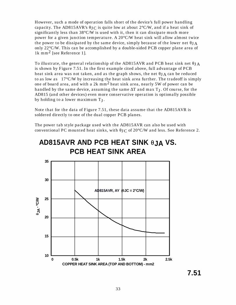
However, such a mode of operation falls short of the device’s full power handlingcapacity. The AD815AVR’s θJC is quite low at about 2°C/W, and if a heat sink ofsignificantly less than 38°C/W is used with it, then it can dissipate much morepower for a given junction temperature. A 20°C/W heat sink will allow almost twicethe power to be dissipated by the same device, simply because of the lower net θJAonly 22°C/W. This can be accomplished by a double-sided PCB copper plane area of1k mm2 [see Reference 1].
To illustrate, the general relationship of the AD815AVR and PCB heat sink net θJAis shown by Figure 7.51. In the first example cited above, full advantage of PCBheat sink area was not taken, and as the graph shows, the net θJA can be reducedto as low as ≅17°C/W by increasing the heat sink area further. The tradeoff is simplyone of board area, and with a 2k mm2 heat sink area, nearly 5W of power can behandled by the same device, assuming the same ∆T and max TJ. Of course, for theAD815 (and other devices) even more conservative operation is optionally possibleby holding to a lower maximum TJ.
Note that for the data of Figure 7.51, these data assume that the AD815AVR issoldered directly to one of the dual copper PCB planes.
The power tab style package used with the AD815AVR can also be used withconventional PC mounted heat sinks, with θJC of 20°C/W and less. See Reference 2.
COPPER HEAT SINK AREA (TOP AND BOTTOM) mm2
35
30
100 2.5k0.5k 1k 1.5k 2k
25
20
15
AD815AVR, AY (θθJC = 2°C/W)
7.51
AD815AVR AND PCB HEAT SINK θθJA VS.PCB HEAT SINK AREA
θθ JA
- ºC
/W
34
Calculating Power In Various Devices
In all instances of thermal calculations, a basic assumption is that the power is thetotal for a given package. With many modern devices now using more than onesupply, the net total power dissipated will be the sum of all individual supplyquiescent powers, plus any load dependent power. For many low output current opamps for example, total power will then be essentially the same as the quiescent. Aslong as this is safely less than the package can support, there is little worry.However, with some devices operable over a wide range of supply voltages, there areinstances where high supply voltages and a medium to high quiescent current plusload current can be a problem.
The AD811 is such an example, being capable of operation from ±5V to ±15V, with aquiescent current of about 16mA. If operated at ±15V, the quiescent dissipation isnearly 500mW, which with a 90°C/W θJA, will push TJ to about 115°C in a 70°Cambient, high enough for concern. If the signal voltage output for such an amplifierdoesn’t require the ±15V supplies, then reducing the supplies will lower thequiescent power, and TJ.
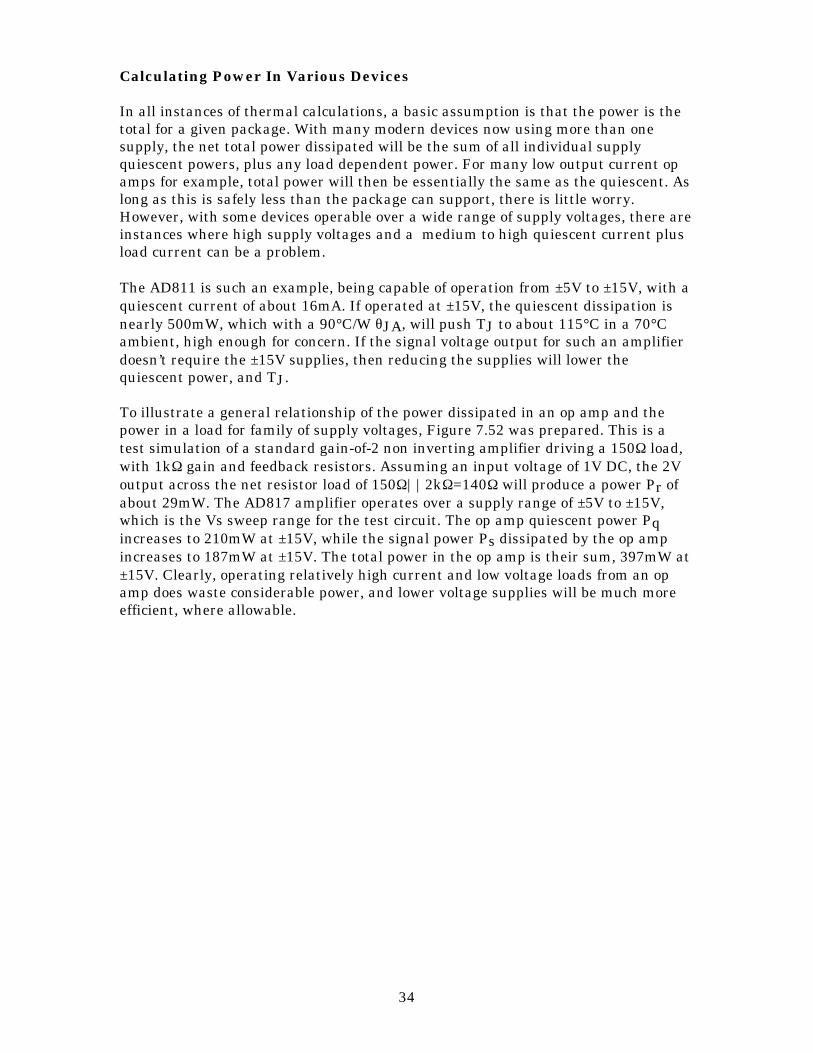
To illustrate a general relationship of the power dissipated in an op amp and thepower in a load for family of supply voltages, Figure 7.52 was prepared. This is atest simulation of a standard gain-of-2 non inverting amplifier driving a 150Ω load,with 1kΩ gain and feedback resistors. Assuming an input voltage of 1V DC, the 2Voutput across the net resistor load of 150Ω||2kΩ=140Ω will produce a power Pr ofabout 29mW. The AD817 amplifier operates over a supply range of ±5V to ±15V,which is the Vs sweep range for the test circuit. The op amp quiescent power Pqincreases to 210mW at ±15V, while the signal power Ps dissipated by the op ampincreases to 187mW at ±15V. The total power in the op amp is their sum, 397mW at±15V. Clearly, operating relatively high current and low voltage loads from an opamp does waste considerable power, and lower voltage supplies will be much moreefficient, where allowable.
35
a
AD817 OP AMP POWER DISSIPATION VS. SUPPLY VOLTAGE
7.52
+
-
AD817
+2V
150ΩΩ
1kΩΩ
+1V
1kΩΩ
+VS
-VS
POWER(mW)
±VS, VOLTS
400
300
200
100
0
0 5 10 15
Ps + Pq = TOTALOP AMP POWER
Pq = QUIESCENT POWER
Ps = SIGNAL POWER
Pr = LOAD POWER
Where appropriate, a clip on DIP compatible heat sink such as the AAVID 580100can be used [Reference 3]. This series has sinks compatible with ICs of 8 through 40pin sizes, using a staggered fin design. Performance of these (and all) heat sinks isenhanced by air movement, either through forced convection, or as a minimum, byarranging PCB cards vertically to enhance natural convection.
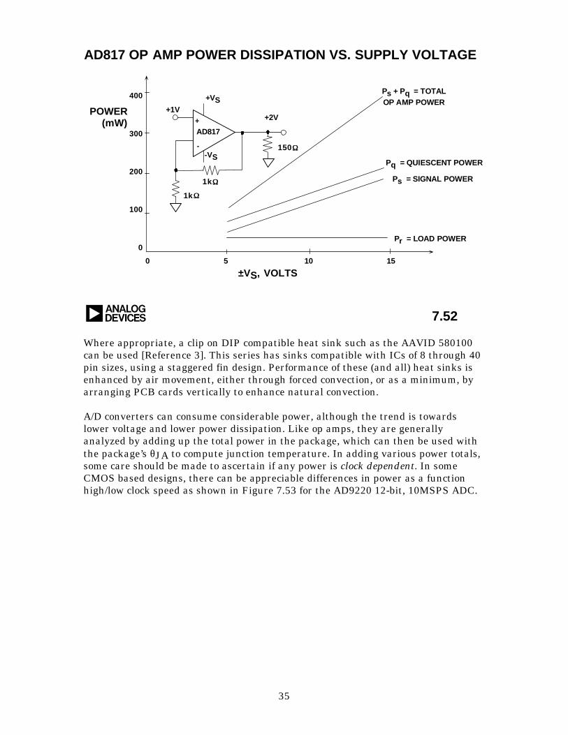
A/D converters can consume considerable power, although the trend is towardslower voltage and lower power dissipation. Like op amps, they are generallyanalyzed by adding up the total power in the package, which can then be used withthe package’s θJA to compute junction temperature. In adding various power totals,some care should be made to ascertain if any power is clock dependent. In someCMOS based designs, there can be appreciable differences in power as a functionhigh/low clock speed as shown in Figure 7.53 for the AD9220 12-bit, 10MSPS ADC.
36
7.53
AD9220 12-BIT, 10MSPS CMOS ADC POWER DISSIPATIONVS. SAMPLING CLOCK FREQUENCY
aCLOCK FREQUENCY MHz
300
240
1210
280
260
INPUT = 5Vp-p
INPUT = 2Vp-p
220
20086420 14
PO
WE
R -
mW
For example, the AD9042 12 bit A/D consumes about 600mW total on two 5Vsupplies, and its 28 pin DIP package has a θJA of 34°C/W. What will be the max TJfor this part in a TA of 70°C? You should get a TJ of 90.4°C (∆T = 0.6W × 34°C/W =20.4°C, so TJ for TA of 70°C = 70°C + 20.4°C). This particular part is therefore ingood shape for this TA, assuming that there are no adjacent “hot spot” sources toincrease the device’s effective TA.
Airflow Control
For large power dissipations and/or to maintain low TJ’s, forced air movement canbe used to increase air flow and aid in heat removal. In its most simple form this canconsist of a continuously or thermostatically operated fan, directed across hightemperature, high wattage dissipation devices such as CPUs, DSP chips, etc.
Quite often however, more sophisticated temperature control is necessary. Recenttemperature monitoring and control ICs such as the TMP12, an airflow temperaturesensor IC, lend themselves to such applications.
The TMP12 includes on chip two comparators, a voltage reference, a temperaturesensor and a heater. The heater is used to force a predictable internal temperaturerise, to match a power IC such as a microprocessor. The temperature sensing andcontrol portions of the IC can then be programmed to respond to the temperaturechanges and control an external fan, so as to maintain some range of temperature.Compared to a simple thermostat, this allows infinite resolution of user control forcontrol points and ON/OFF hysteresis.
The device is placed in an airstream near the power IC, such that both see the samestream of air, and will thus have like temperature profiles, assuming proper controlof the stream. This is shown in basic form by the layout diagram of Figure 7.54.
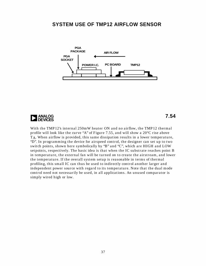
37
7.54
SYSTEM USE OF TMP12 AIRFLOW SENSOR
a
POWER I.C.
PGAPACKAGE
PGA SOCKET
PC BOARD
AIR FLOW
TMP12
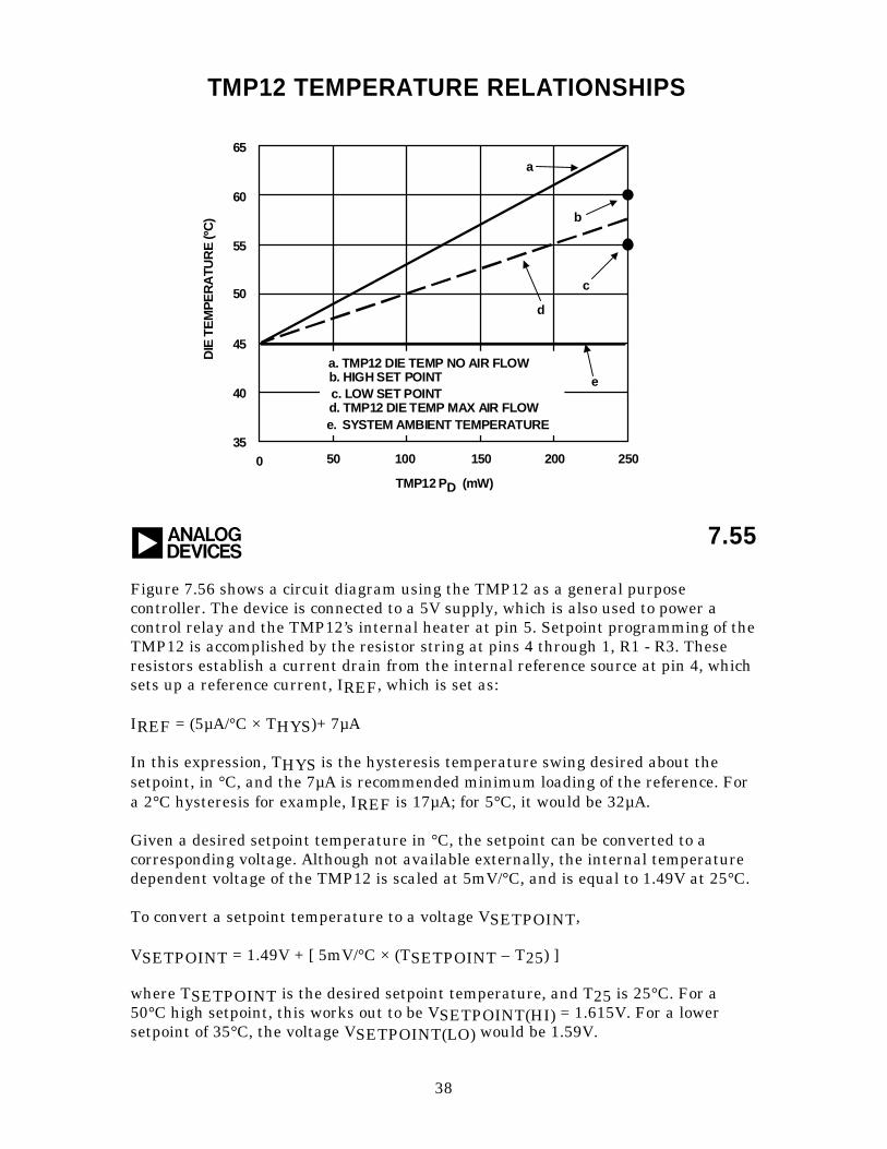
With the TMP12’s internal 250mW heater ON and no airflow, the TMP12 thermalprofile will look like the curve “A” of Figure 7.55, and will show a 20°C rise aboveTA. When airflow is provided, this same dissipation results in a lower temperature,“D”. In programming the device for airspeed control, the designer can set up to twoswitch points, shown here symbolically by “B” and “C”, which are HIGH and LOWsetpoints, respectively. The basic idea is that when the IC substrate reaches point Bin temperature, the external fan will be turned on to create the airstream, and lowerthe temperature. If the overall system setup is reasonable in terms of thermalprofiling, this small IC can thus be used to indirectly control another larger andindependent power source with regard to its temperature. Note that the dual modecontrol need not necessarily be used, in all applications. An unused comparator issimply wired high or low.
38
7.55
TMP12 TEMPERATURE RELATIONSHIPS
a
35
40
45
50
55
60
65
50 100 150 200 2500
TMP12 PD (mW)
a. TMP12 DIE TEMP NO AIR FLOW
c. LOW SET POINTb. HIGH SET POINT
d. TMP12 DIE TEMP MAX AIR FLOWe. SYSTEM AMBIENT TEMPERATURE
a
b
c
d
e
DIE
TE
MP
ER
ATU
RE
(ºC
)
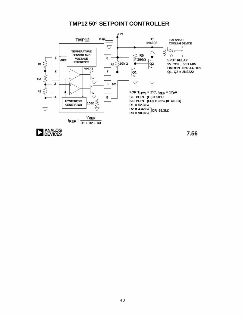
Figure 7.56 shows a circuit diagram using the TMP12 as a general purposecontroller. The device is connected to a 5V supply, which is also used to power acontrol relay and the TMP12’s internal heater at pin 5. Setpoint programming of theTMP12 is accomplished by the resistor string at pins 4 through 1, R1 - R3. Theseresistors establish a current drain from the internal reference source at pin 4, whichsets up a reference current, IREF, which is set as:
IREF = (5µA/°C × THYS)+ 7µA
In this expression, THYS is the hysteresis temperature swing desired about thesetpoint, in °C, and the 7µA is recommended minimum loading of the reference. Fora 2°C hysteresis for example, IREF is 17µA; for 5°C, it would be 32µA.
Given a desired setpoint temperature in °C, the setpoint can be converted to acorresponding voltage. Although not available externally, the internal temperaturedependent voltage of the TMP12 is scaled at 5mV/°C, and is equal to 1.49V at 25°C.
To convert a setpoint temperature to a voltage VSETPOINT,
VSETPOINT = 1.49V + [ 5mV/°C × (TSETPOINT – T25) ]
where TSETPOINT is the desired setpoint temperature, and T25 is 25°C. For a50°C high setpoint, this works out to be VSETPOINT(HI) = 1.615V. For a lowersetpoint of 35°C, the voltage VSETPOINT(LO) would be 1.59V.
39
The divider resistors are then chosen to draw the required current IREF whilesetting the two tap voltages corresponding to VSETPOINT(HI) andVSETPOINT(LO).
RTOTAL = VREF / IREF = 2.5V / IREF
R1 = [ VREF – VSETPOINT(HI) ] / IREF = [ 2.5V – VSETPOINT(HI) ] / IREF
R2= [ VSETPOINT(HI) – VSETPOINT(LO) ] / IREF
R3 = VSETPOINT(LO) / IREF
In the example of the figure, the resulting standard values for R1 - R3 correspond tothe temperature/voltage setpoint examples noted above. Ideal 1% values shown giveresistor related errors of only 0.1°C from ideal. Note that this is error is independentof the TMP12 temperature errors, which are ±2°C.
As noted above, both comparators of the device need not always be used, and in thiscase the lower comparator output is not used. For a single point 50°C controller, the35°C setpoint is superfluous. One resistor can be eliminated by making R2 + R3 asingle value of 95.3kΩ and connecting pin 3 to GND. Pin 6 should be left as a no-connect. If a greater hysteresis is desired, the resistor values will be proportionallylowered.
It is also important to minimize potential parasitic temperature errors associatedwith the TMP12. Although the open-collector outputs can sink up to 20mA, it isadvised that currents be kept low at this node, to limit any additional temperaturerise. The Q1 - Q2 transistor buffer shown in the figure raises the current drive to100mA, allowing a 50Ω/5V coil to be driven. The relay type shown is generalpurpose, and many other power interfaces are possible with the TMP12. If used asshown, the relay contacts would be used to turn on a fan for airflow when the activelow output at pin 7 changes, indicating the upper setpoint threshold.
A basic assumption of the TMP12’s operation is that it will “mimic” another devicein temperature rise. Therefore, a practical working system must be arranged andtested for proper airflow channeling, minimal disturbances from adjacent devices,etc. Some experimentation should be expected before a final setup will result.
40
a
TMP12 50º SETPOINT CONTROLLER
7.56
Q2
R5390ΩΩ
0.1µµF
100ΩΩ
1
2
3
4 5
6
7
8
HYSTERESISGENERATOR
+
-
-
+
VPTAT
R1
R2
R3
VREF
TEMPERATURESENSOR AND
VOLTAGEREFERENCE
TMP12
+5V
R4 10kΩΩ
Q1
D1IN4002
TO FAN ORCOOLING DEVICE
SPDT RELAY5V COIL, 50ΩΩ MINOMRON G2R-14-DC5Q1, Q2 = 2N2222
FOR THYS = 2ºC, IREF = 17µµASETPOINT (HI) = 50ºCSETPOINT (LO) = 35ºC (IF USED)R1 = 52.3kΩΩR2 = 4.42kΩΩR3 = 90.9kΩΩ
OR 95.3kΩΩ
NC
IREF =VREF
R1 + R2 + R3
41
REFERENCES: THERMAL MANAGEMENT
1. Power Consideration Discussions, AD815 Data Sheet, Analog Devices.
2. Heat Sinks for Multiwatt Packages, AAVID Engineering, Inc., One KoolPath, Laconia, NH, 03246, (603) 528-3400.
3. General Catalog, AAVID Engineering, Inc., One Kool Path, Laconia, NH,03246, (603) 528-3400.
42
EMI/RFI CONSIDERATIONS
Adolfo A. Garcia
Electromagnetic interference (EMI) has become a hot topic in the last few yearsamong circuit designers and systems engineers. Although the subject matter andprior art have been in existence for over the last 50 years or so, the advent ofportable and high-frequency industrial and consumer electronics has provided acomfortable standard of living for many EMI testing engineers, consultants, andpublishers. With the help of EDN Magazine and Kimmel Gerke Associates, thissection will highlight general issues of EMC (electromagnetic compatibility) tofamiliarize the system/circuit designer with this subject and to illustrate proventechniques for protection against EMI.
A PRIMER ON EMI REGULATIONS
The intent of this section is to summarize the different types of electromagneticcompatibility (EMC) regulations imposed on equipment manufacturers, bothvoluntary and mandatory. Published EMC regulations apply at this time only toequipment and systems, and not to components. Thus, EMI hardened equipmentdoes not necessarily imply that each of the components used (integrated circuits,especially) in the equipment must also be EMI hardened.
Commercial Equipment
The two driving forces behind commercial EMI regulations are the FCC (FederalCommunications Commission) in the U. S. and the VDE (Verband DeutscherElectrotechniker) in Germany. VDE regulations are more restrictive than the FCC’swith regard to emissions and radiation, but the European Community will beadding immunity to RF, electrostatic discharge, and power-line disturbances to theVDE regulations, and now requires mandatory compliance. In Japan, commercialEMC regulations are covered under the VCCI (Voluntary Control Council forInterference) standards and, implied by the name, are much looser than their FCCand VDE counterparts.
All commercial EMI regulations primarily focus on radiated emissions, specifically toprotect nearby radio and television receivers, although both FCC and VDEstandards are less stringent with respect to conducted interference (by a factor of 10over radiated levels). The FCC Part 15 and VDE 0871 regulations group commercialequipment into two classes: Class A, for all products intended for businessenvironments; and Class B, for all products used in residential applications. Forexample, Table 7.1 illustrates the electric-field emission limits of commercialcomputer equipment for both FCC Part 15 and VDE 0871 compliance.
Radiated Emission Limits for Commercial Computer Equipment
Frequency (MHz) Class A Class B

43
( at 3 m) (at 3 m)30 - 88 300 µV/m 100 µV/m
88 - 216 500 µV/m 150 µV/m216 - 1000 700 µV/m 200 µV/m
Reprinted from EDN Magazine (January 20, 1994), © CAHNERS PUBLISHINGCOMPANY 1995, A Division of Reed Publishing USA.
Table 7.1
In addition to the already stringent VDE emission limits, the European CommunityEMC standards (IEC and IEEE) now requires mandatory compliance to theseadditional EMI threats: Immunity to RF fields, electrostatic discharge, and power-line disturbances. All equipment/systems marketed in Europe must exhibit animmunity to RF field strengths of 1-10V/m (IEC standard 801-3), electrostaticdischarge (generated by human contact or through material movement) in the rangeof 10-15kV (IEC standard 801-2), and power-line disturbances of 4kV EFTs(extremely fast transients, IEC standard 801-4) and 6kV lightning surges (IEEEstandard C62.41).
Military Equipment
The defining EMC specification for military equipment is MIL-STD-461 whichapplies to radiated equipment emissions and equipment susceptibility tointerference. Radiated emission limits are very typically 10 to 100 times morestringent than the levels shown in Table 7.1. Required limits on immunity to RFfields are typically 200 times more stringent (RF field strengths of 5-50mV/m) thanthe limits for commercial equipment.
Medical Equipment
Although not yet mandatory, EMC regulations for medical equipment are presentlybeing defined by the FDA (Food and Drug Administration) in the USA and theEuropean Community. The primary focus of these EMC regulations will be onimmunity to RF fields, electrostatic discharge, and power-line disturbances, andmay very well be more stringent than the limits spelled out in MIL-STD-461. Theprimary objective of the medical EMC regulations is to guarantee safety to humans.
Industrial- and Process-Control Equipment
Presently, equipment designed and marketed for industrial- and process-controlapplications are not required to meet pre-existing mandatory EMC regulations. Infact, manufacturers are exempt from complying to any standard in the USA.However, since industrial environments are very much electrically hostile, allequipment manufacturers will be required to comply with all European CommunityEMC regulations in 1996.
Automotive Equipment
Perhaps the most difficult and hostile environment in which electrical circuits andsystems must operate is that found in the automobile. All of the key EMI threats to

44
electrical systems exist here. In addition, operating temperature extremes, moisture,dirt, and toxic chemicals further exacerbate the problem. To complicate mattersfurther, standard techniques (ferrite beads, feed-through capacitors, inductors,resistors, shielded cables, wires, and connectors) used in other systems are notgenerally used in automotive applications because of the cost of the additionalcomponents.
Presently, automotive EMC regulations, defined by the very comprehensive SAEStandards J551 and J1113, are not yet mandatory. They are, however, veryrigorous. SAE standard J551 applies to vehicle-level EMC specifications, andstandard J1113 (functionally similar to MIL-STD-461) applies to all automotiveelectronic modules. For example, the J1113 specification requires that electronicmodules cannot radiate electric fields greater than 300nV/m at a distance of 3meters. This is roughly 1000 times more stringent than the FCC Part 15 Class Aspecification. In many applications, automotive manufacturers are imposing J1113RF field immunity limits on each of the active components used in these modules.Thus, in the very near future, automotive manufacturers will require that ICproducts comply with existing EMC standards and regulations.
EMC Regulations’ Impact on Design
In all these applications and many more, complying with mandatory EMCregulations will require careful design of individual circuits, modules, and systemsusing established techniques for cable shielding, signal and power-line filteringagainst both small- and large-scale disturbances, and sound multi-layer PCBlayouts. The key to success is to incorporate sound EMC principles early in thedesign phase to avoid time-consuming and expensive redesign efforts.
A DIAGNOSTIC FRAMEWORK FOR EMI/RFI PROBLEM
SOLVING
With any problem, a strategy should be developed before any effort is expendedtrying to solve it. This approach is similar to the scientific method: initial circuitmisbehavior is noted, theories are postulated, experiments designed to test thetheories are conducted, and results are again noted. This process continues until alltheories have been tested and expected results achieved and recorded. With respectto EMI, a problem solving framework has been developed. As shown in Figure 7.57,the model suggested by Kimmel-Gerke in [Reference 1] illustrates that all threeelements (a source, a receptor or victim, and a path between the two) must exist inorder to be considered an EMI problem. The sources of electromagnetic interferencecan take on many forms, and the ever-increasing number of portableinstrumentation and personal communications/computation equipment only addsthe number of possible sources and receptors.
A DIAGNOSTIC FRAMEWORK FOR EMIReprinted from EDN Magazine (January 20,1994), © CAHNERS PUBLISHING COMPANY
1995, A Division of Reed Publishing USA
ANY INTERFERENCE PROBLEM CAN BE BROKEN DOWN INTO:
nn The SOURCE of interference
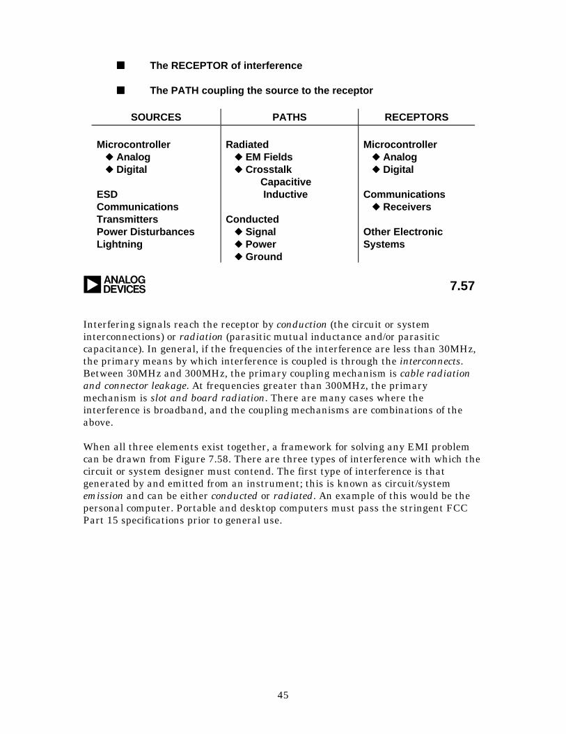
45
nn The RECEPTOR of interference
nn The PATH coupling the source to the receptor
SOURCES PATHS RECEPTORS
Microcontroller uu Analog uu Digital
ESDCommunicationsTransmittersPower DisturbancesLightning
Radiated uu EM Fields uu Crosstalk Capacitive Inductive
Conducted uu Signal uu Power uu Ground
Microcontroller uu Analog uu Digital
Communications uu Receivers
Other ElectronicSystems
a 7.57
Interfering signals reach the receptor by conduction (the circuit or systeminterconnections) or radiation (parasitic mutual inductance and/or parasiticcapacitance). In general, if the frequencies of the interference are less than 30MHz,the primary means by which interference is coupled is through the interconnects.Between 30MHz and 300MHz, the primary coupling mechanism is cable radiationand connector leakage. At frequencies greater than 300MHz, the primarymechanism is slot and board radiation. There are many cases where theinterference is broadband, and the coupling mechanisms are combinations of theabove.
When all three elements exist together, a framework for solving any EMI problemcan be drawn from Figure 7.58. There are three types of interference with which thecircuit or system designer must contend. The first type of interference is thatgenerated by and emitted from an instrument; this is known as circuit/systememission and can be either conducted or radiated. An example of this would be thepersonal computer. Portable and desktop computers must pass the stringent FCCPart 15 specifications prior to general use.
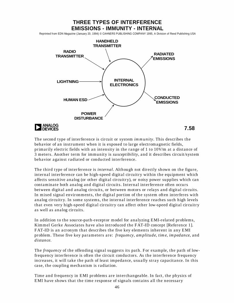
46
THREE TYPES OF INTERFERENCEEMISSIONS - IMMUNITY - INTERNAL
7.58a
Reprinted from EDN Magazine (January 20, 1994) © CAHNERS PUBLISHING COMPANY 1995, A Division of Reed Publishing USA
RADIOTRANSMITTER
HANDHELDTRANSMITTER
RADIATEDEMISSIONS
CONDUCTEDEMISSIONS
LIGHTNING
HUMAN ESD
POWERDISTURBANCE
INTERNALELECTRONICS
The second type of interference is circuit or system immunity. This describes thebehavior of an instrument when it is exposed to large electromagnetic fields,primarily electric fields with an intensity in the range of 1 to 10V/m at a distance of3 meters. Another term for immunity is susceptibility, and it describes circuit/systembehavior against radiated or conducted interference.
The third type of interference is internal. Although not directly shown on the figure,internal interference can be high-speed digital circuitry within the equipment whichaffects sensitive analog (or other digital circuitry), or noisy power supplies which cancontaminate both analog and digital circuits. Internal interference often occursbetween digital and analog circuits, or between motors or relays and digital circuits.In mixed signal environments, the digital portion of the system often interferes withanalog circuitry. In some systems, the internal interference reaches such high levelsthat even very high-speed digital circuitry can affect other low-speed digital circuitryas well as analog circuits.
In addition to the source-path-receptor model for analyzing EMI-related problems,Kimmel Gerke Associates have also introduced the FAT-ID concept [Reference 1].FAT-ID is an acronym that describes the five key elements inherent in any EMIproblem. These five key parameters are: frequency, amplitude, time, impedance, anddistance.
The frequency of the offending signal suggests its path. For example, the path of low-frequency interference is often the circuit conductors. As the interference frequencyincreases, it will take the path of least impedance, usually stray capacitance. In thiscase, the coupling mechanism is radiation.
Time and frequency in EMI problems are interchangeable. In fact, the physics ofEMI have shows that the time response of signals contains all the necessary

47
information to construct the spectral response of the interference. In digital systems,both the signal rise time and pulse repetition rate produce spectral componentsaccording to the following relationship:
fEMI1trise
=⋅π
Eq. 7.1
For example, a pulse having a 1ns rise time is equivalent to an EMI frequency ofover 300MHz. This time-frequency relationship can also be applied to high-speedanalog circuits, where slew rates in excess of 1000V/µs and gain-bandwidth productsgreater than 500MHz are not uncommon.
When this concept is applied to instruments and systems, EMI emissions are againfunctions of signal rise time and pulse repetition rates. Spectrum analyzers and highspeed oscilloscopes used with voltage and current probes are very useful tools inquantifying the effects of EMI on circuits and systems.
Another important parameter in the analysis of EMI problems is the physicaldimensions of cables, wires, and enclosures. Cables can behave as either passiveantennas (receptors) or very efficient transmitters (sources) of interference. Theirphysical length and their shield must be carefully examined where EMI is a concern.As previously mentioned, the behavior of simple conductors is a function of length,cross-sectional area, and frequency. Openings in equipment enclosures can behaveas slot antennas, thereby allowing EMI energy to affect the internal electronics.
PASSIVE COMPONENTS: YOUR ARSENAL AGAINST EMI
Minimizing the effects of EMI requires that the circuit/system designer becompletely aware of the primary arsenal in the battle against interference: passivecomponents. To use successfully these components, the designer must understandtheir non-ideal behavior. For example, Figure 7.59 illustrates the real behavior ofthe passive components used in circuit design. At very high frequencies, wiresbecome transmission lines, capacitors become inductors, inductors becomecapacitors, and resistors behave as resonant circuits.
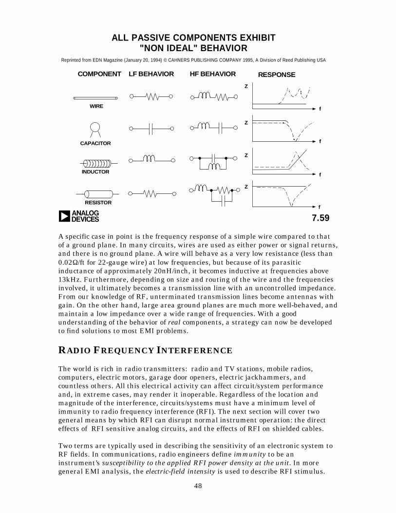
48
ALL PASSIVE COMPONENTS EXHIBIT"NON IDEAL" BEHAVIOR
7.59a
Reprinted from EDN Magazine (January 20, 1994) © CAHNERS PUBLISHING COMPANY 1995, A Division of Reed Publishing USA
WIRE
COMPONENT LF BEHAVIOR HF BEHAVIOR RESPONSE
CAPACITOR
INDUCTOR
RESISTOR
Z
Z
Z
Z
f
f
f
f
A specific case in point is the frequency response of a simple wire compared to thatof a ground plane. In many circuits, wires are used as either power or signal returns,and there is no ground plane. A wire will behave as a very low resistance (less than0.02Ω/ft for 22-gauge wire) at low frequencies, but because of its parasiticinductance of approximately 20nH/inch, it becomes inductive at frequencies above13kHz. Furthermore, depending on size and routing of the wire and the frequenciesinvolved, it ultimately becomes a transmission line with an uncontrolled impedance.From our knowledge of RF, unterminated transmission lines become antennas withgain. On the other hand, large area ground planes are much more well-behaved, andmaintain a low impedance over a wide range of frequencies. With a goodunderstanding of the behavior of real components, a strategy can now be developedto find solutions to most EMI problems.
RADIO FREQUENCY INTERFERENCE
The world is rich in radio transmitters: radio and TV stations, mobile radios,computers, electric motors, garage door openers, electric jackhammers, andcountless others. All this electrical activity can affect circuit/system performanceand, in extreme cases, may render it inoperable. Regardless of the location andmagnitude of the interference, circuits/systems must have a minimum level ofimmunity to radio frequency interference (RFI). The next section will cover twogeneral means by which RFI can disrupt normal instrument operation: the directeffects of RFI sensitive analog circuits, and the effects of RFI on shielded cables.
Two terms are typically used in describing the sensitivity of an electronic system toRF fields. In communications, radio engineers define immunity to be aninstrument’s susceptibility to the applied RFI power density at the unit. In moregeneral EMI analysis, the electric-field intensity is used to describe RFI stimulus.
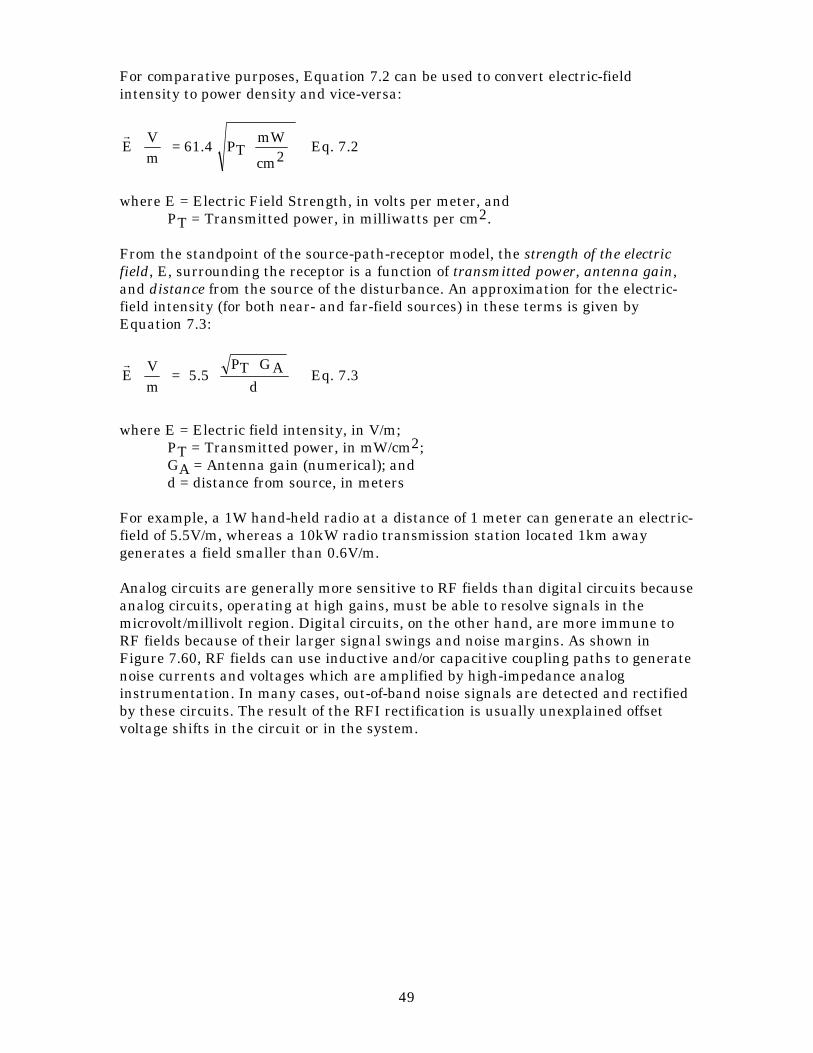
49
For comparative purposes, Equation 7.2 can be used to convert electric-fieldintensity to power density and vice-versa:
rE
Vm
61.4 PTmW
cm2
=
Eq. 7.2
where E = Electric Field Strength, in volts per meter, andPT = Transmitted power, in milliwatts per cm2.
From the standpoint of the source-path-receptor model, the strength of the electricfield, E, surrounding the receptor is a function of transmitted power, antenna gain,and distance from the source of the disturbance. An approximation for the electric-field intensity (for both near- and far-field sources) in these terms is given byEquation 7.3:
rE
Vm
5.5PT
=⋅
GAd
Eq. 7.3
where E = Electric field intensity, in V/m;PT = Transmitted power, in mW/cm2;GA = Antenna gain (numerical); andd = distance from source, in meters
For example, a 1W hand-held radio at a distance of 1 meter can generate an electric-field of 5.5V/m, whereas a 10kW radio transmission station located 1km awaygenerates a field smaller than 0.6V/m.
Analog circuits are generally more sensitive to RF fields than digital circuits becauseanalog circuits, operating at high gains, must be able to resolve signals in themicrovolt/millivolt region. Digital circuits, on the other hand, are more immune toRF fields because of their larger signal swings and noise margins. As shown inFigure 7.60, RF fields can use inductive and/or capacitive coupling paths to generatenoise currents and voltages which are amplified by high-impedance analoginstrumentation. In many cases, out-of-band noise signals are detected and rectifiedby these circuits. The result of the RFI rectification is usually unexplained offsetvoltage shifts in the circuit or in the system.
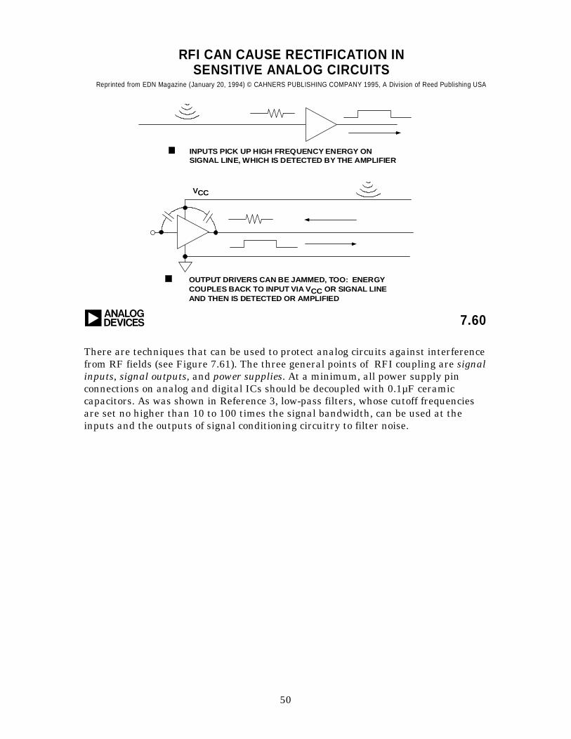
50
RFI CAN CAUSE RECTIFICATION INSENSITIVE ANALOG CIRCUITS
7.60a
Reprinted from EDN Magazine (January 20, 1994) © CAHNERS PUBLISHING COMPANY 1995, A Division of Reed Publishing USA
VCC
INPUTS PICK UP HIGH FREQUENCY ENERGY ONSIGNAL LINE, WHICH IS DETECTED BY THE AMPLIFIER
OUTPUT DRIVERS CAN BE JAMMED, TOO: ENERGYCOUPLES BACK TO INPUT VIA VCC OR SIGNAL LINEAND THEN IS DETECTED OR AMPLIFIED
There are techniques that can be used to protect analog circuits against interferencefrom RF fields (see Figure 7.61). The three general points of RFI coupling are signalinputs, signal outputs, and power supplies. At a minimum, all power supply pinconnections on analog and digital ICs should be decoupled with 0.1µF ceramiccapacitors. As was shown in Reference 3, low-pass filters, whose cutoff frequenciesare set no higher than 10 to 100 times the signal bandwidth, can be used at theinputs and the outputs of signal conditioning circuitry to filter noise.
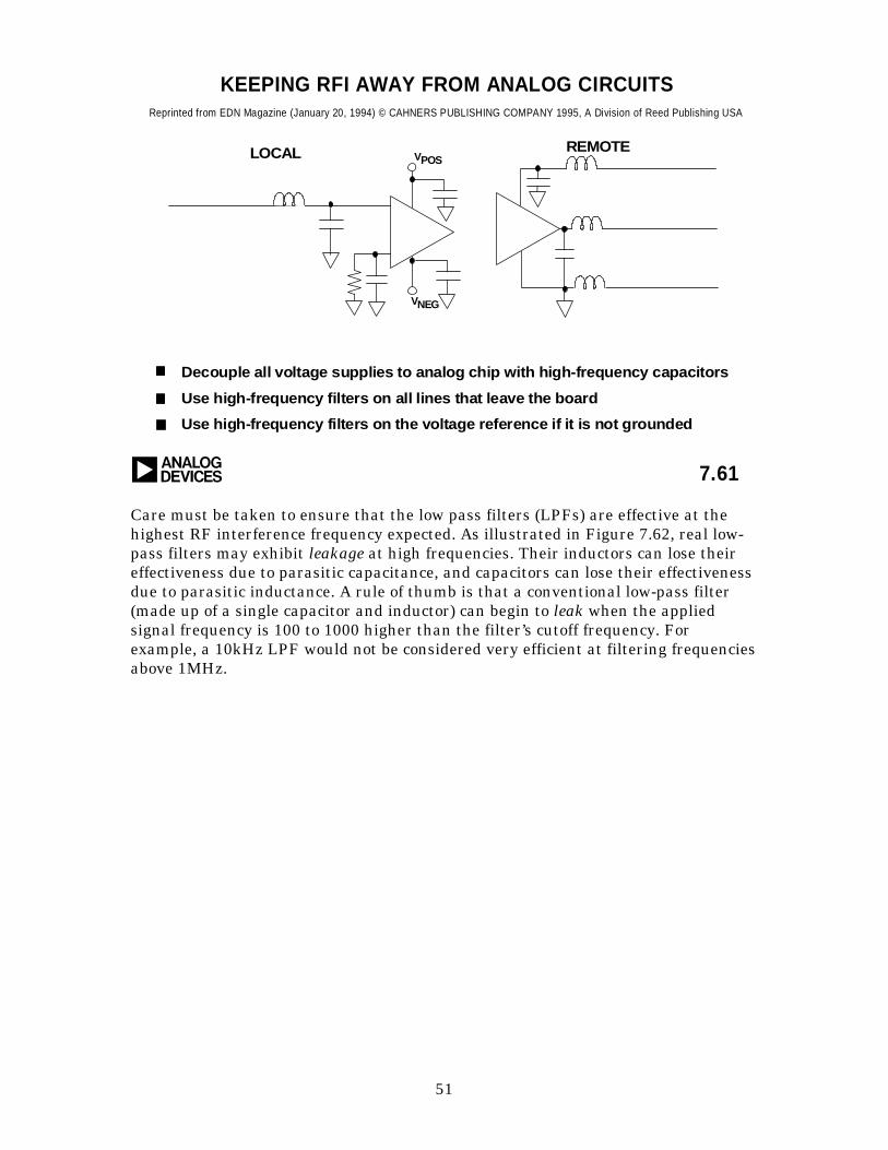
51
VPOS
KEEPING RFI AWAY FROM ANALOG CIRCUITS
7.61a
Reprinted from EDN Magazine (January 20, 1994) © CAHNERS PUBLISHING COMPANY 1995, A Division of Reed Publishing USA
Decouple all voltage supplies to analog chip with high-frequency capacitors
Use high-frequency filters on all lines that leave the board
Use high-frequency filters on the voltage reference if it is not grounded
LOCAL REMOTE
VNEG
Care must be taken to ensure that the low pass filters (LPFs) are effective at thehighest RF interference frequency expected. As illustrated in Figure 7.62, real low-pass filters may exhibit leakage at high frequencies. Their inductors can lose theireffectiveness due to parasitic capacitance, and capacitors can lose their effectivenessdue to parasitic inductance. A rule of thumb is that a conventional low-pass filter(made up of a single capacitor and inductor) can begin to leak when the appliedsignal frequency is 100 to 1000 higher than the filter’s cutoff frequency. Forexample, a 10kHz LPF would not be considered very efficient at filtering frequenciesabove 1MHz.
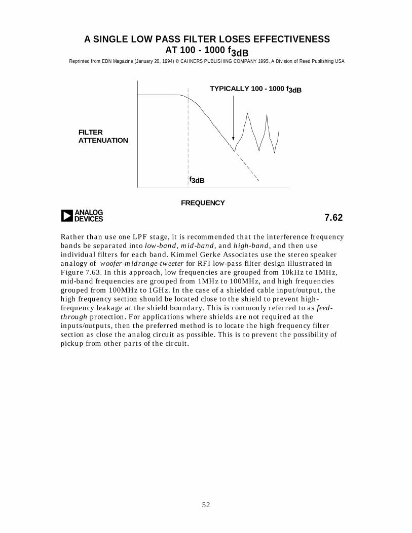
52
A SINGLE LOW PASS FILTER LOSES EFFECTIVENESSAT 100 - 1000 f3dB
7.62a
Reprinted from EDN Magazine (January 20, 1994) © CAHNERS PUBLISHING COMPANY 1995, A Division of Reed Publishing USA
TYPICALLY 100 - 1000 f3dB
f3dB
FREQUENCY
FILTERATTENUATION
Rather than use one LPF stage, it is recommended that the interference frequencybands be separated into low-band, mid-band, and high-band, and then useindividual filters for each band. Kimmel Gerke Associates use the stereo speakeranalogy of woofer-midrange-tweeter for RFI low-pass filter design illustrated inFigure 7.63. In this approach, low frequencies are grouped from 10kHz to 1MHz,mid-band frequencies are grouped from 1MHz to 100MHz, and high frequenciesgrouped from 100MHz to 1GHz. In the case of a shielded cable input/output, thehigh frequency section should be located close to the shield to prevent high-frequency leakage at the shield boundary. This is commonly referred to as feed-through protection. For applications where shields are not required at theinputs/outputs, then the preferred method is to locate the high frequency filtersection as close the analog circuit as possible. This is to prevent the possibility ofpickup from other parts of the circuit.
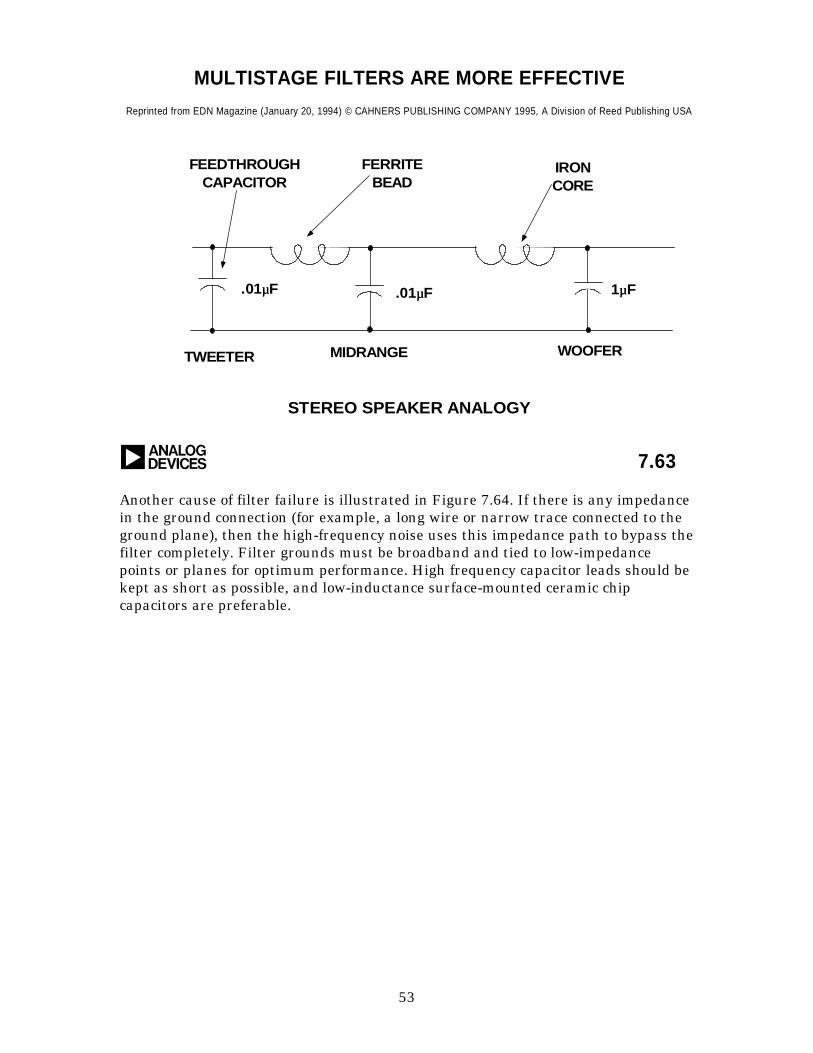
53
MULTISTAGE FILTERS ARE MORE EFFECTIVE
7.63a
Reprinted from EDN Magazine (January 20, 1994) © CAHNERS PUBLISHING COMPANY 1995, A Division of Reed Publishing USA
FERRITEBEAD
IRONCORE
WOOFERMIDRANGE
.01µµF.01µµF
TWEETER
STEREO SPEAKER ANALOGY
FEEDTHROUGHCAPACITOR
1µµF
Another cause of filter failure is illustrated in Figure 7.64. If there is any impedancein the ground connection (for example, a long wire or narrow trace connected to theground plane), then the high-frequency noise uses this impedance path to bypass thefilter completely. Filter grounds must be broadband and tied to low-impedancepoints or planes for optimum performance. High frequency capacitor leads should bekept as short as possible, and low-inductance surface-mounted ceramic chipcapacitors are preferable.
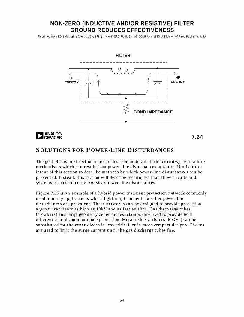
54
NON-ZERO (INDUCTIVE AND/OR RESISTIVE) FILTERGROUND REDUCES EFFECTIVENESS
7.64a
Reprinted from EDN Magazine (January 20, 1994) © CAHNERS PUBLISHING COMPANY 1995, A Division of Reed Publishing USA
HFENERGY
FILTER
BOND IMPEDANCE
HFENERGY
SOLUTIONS FOR POWER-LINE DISTURBANCES
The goal of this next section is not to describe in detail all the circuit/system failuremechanisms which can result from power-line disturbances or faults. Nor is it theintent of this section to describe methods by which power-line disturbances can beprevented. Instead, this section will describe techniques that allow circuits andsystems to accommodate transient power-line disturbances.
Figure 7.65 is an example of a hybrid power transient protection network commonlyused in many applications where lightning transients or other power-linedisturbances are prevalent. These networks can be designed to provide protectionagainst transients as high as 10kV and as fast as 10ns. Gas discharge tubes(crowbars) and large geometry zener diodes (clamps) are used to provide bothdifferential and common-mode protection. Metal-oxide varistors (MOVs) can besubstituted for the zener diodes in less critical, or in more compact designs. Chokesare used to limit the surge current until the gas discharge tubes fire.
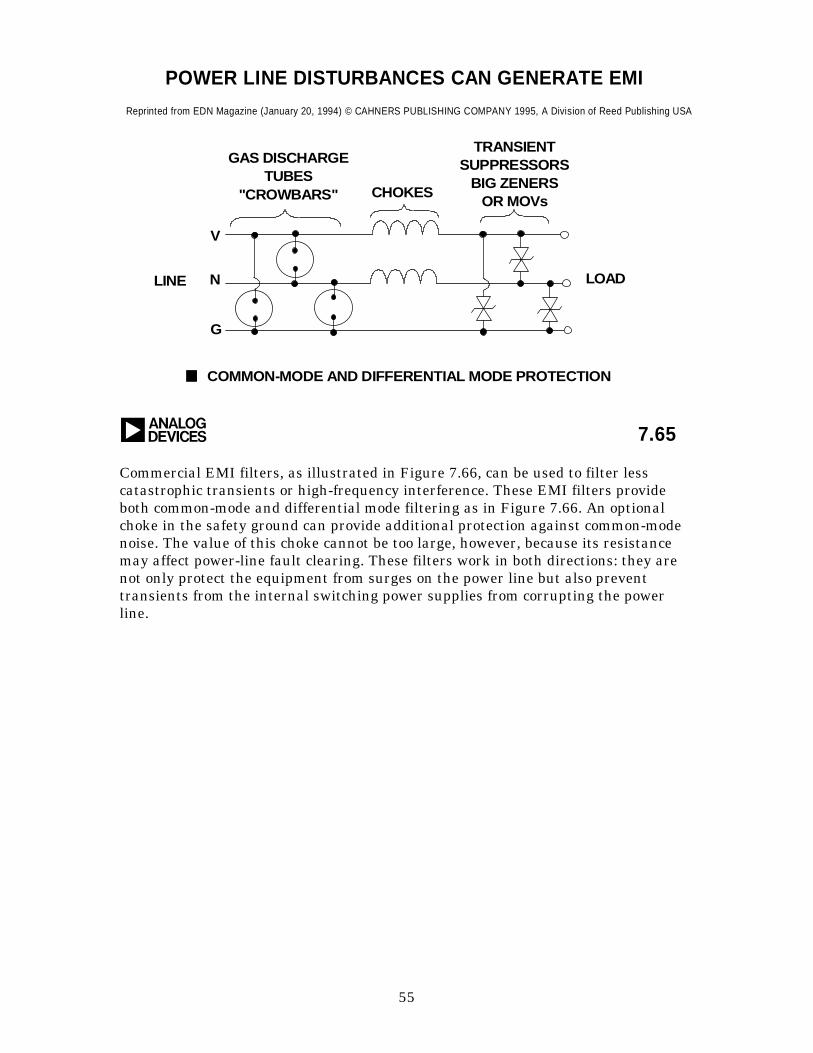
55
POWER LINE DISTURBANCES CAN GENERATE EMI
7.65a
Reprinted from EDN Magazine (January 20, 1994) © CAHNERS PUBLISHING COMPANY 1995, A Division of Reed Publishing USA
COMMON-MODE AND DIFFERENTIAL MODE PROTECTION
GAS DISCHARGETUBES
"CROWBARS" CHOKES
TRANSIENTSUPPRESSORS
BIG ZENERSOR MOVs
V
N
G
LINE LOAD
Commercial EMI filters, as illustrated in Figure 7.66, can be used to filter lesscatastrophic transients or high-frequency interference. These EMI filters provideboth common-mode and differential mode filtering as in Figure 7.66. An optionalchoke in the safety ground can provide additional protection against common-modenoise. The value of this choke cannot be too large, however, because its resistancemay affect power-line fault clearing. These filters work in both directions: they arenot only protect the equipment from surges on the power line but also preventtransients from the internal switching power supplies from corrupting the powerline.
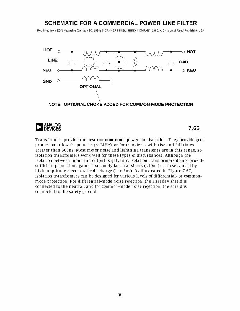
56
SCHEMATIC FOR A COMMERCIAL POWER LINE FILTER
7.66a
Reprinted from EDN Magazine (January 20, 1994) © CAHNERS PUBLISHING COMPANY 1995, A Division of Reed Publishing USA
NOTE: OPTIONAL CHOKE ADDED FOR COMMON-MODE PROTECTION
HOT
NEU
GND
LINE
OPTIONAL
HOT
NEU
LOAD
Transformers provide the best common-mode power line isolation. They provide goodprotection at low frequencies (<1MHz), or for transients with rise and fall timesgreater than 300ns. Most motor noise and lightning transients are in this range, soisolation transformers work well for these types of disturbances. Although theisolation between input and output is galvanic, isolation transformers do not providesufficient protection against extremely fast transients (<10ns) or those caused byhigh-amplitude electrostatic discharge (1 to 3ns). As illustrated in Figure 7.67,isolation transformers can be designed for various levels of differential- or common-mode protection. For differential-mode noise rejection, the Faraday shield isconnected to the neutral, and for common-mode noise rejection, the shield isconnected to the safety ground.
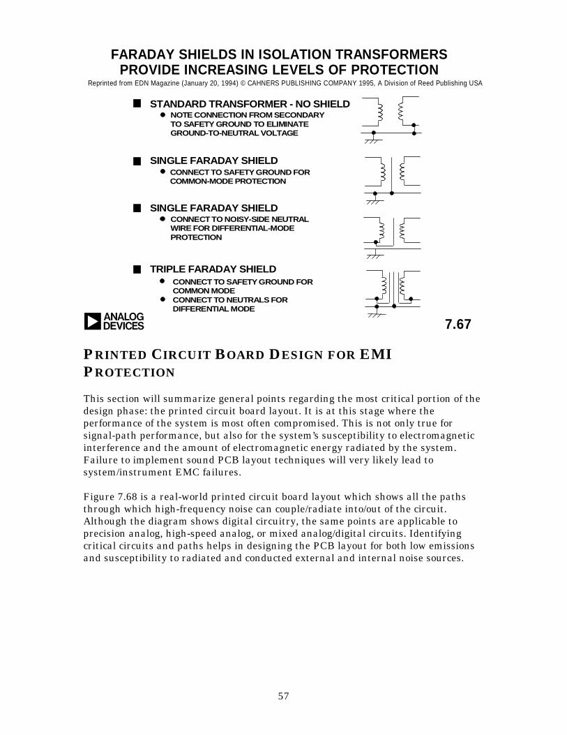
57
FARADAY SHIELDS IN ISOLATION TRANSFORMERSPROVIDE INCREASING LEVELS OF PROTECTION
7.67a
Reprinted from EDN Magazine (January 20, 1994) © CAHNERS PUBLISHING COMPANY 1995, A Division of Reed Publishing USA
SINGLE FARADAY SHIELD
STANDARD TRANSFORMER - NO SHIELD
SINGLE FARADAY SHIELD
TRIPLE FARADAY SHIELD
NOTE CONNECTION FROM SECONDARYTO SAFETY GROUND TO ELIMINATEGROUND-TO-NEUTRAL VOLTAGE
CONNECT TO SAFETY GROUND FORCOMMON-MODE PROTECTION
CONNECT TO NOISY-SIDE NEUTRALWIRE FOR DIFFERENTIAL-MODEPROTECTION
CONNECT TO SAFETY GROUND FORCOMMON MODECONNECT TO NEUTRALS FORDIFFERENTIAL MODE
PRINTED CIRCUIT BOARD DESIGN FOR EMIPROTECTION
This section will summarize general points regarding the most critical portion of thedesign phase: the printed circuit board layout. It is at this stage where theperformance of the system is most often compromised. This is not only true forsignal-path performance, but also for the system’s susceptibility to electromagneticinterference and the amount of electromagnetic energy radiated by the system.Failure to implement sound PCB layout techniques will very likely lead tosystem/instrument EMC failures.
Figure 7.68 is a real-world printed circuit board layout which shows all the pathsthrough which high-frequency noise can couple/radiate into/out of the circuit.Although the diagram shows digital circuitry, the same points are applicable toprecision analog, high-speed analog, or mixed analog/digital circuits. Identifyingcritical circuits and paths helps in designing the PCB layout for both low emissionsand susceptibility to radiated and conducted external and internal noise sources.
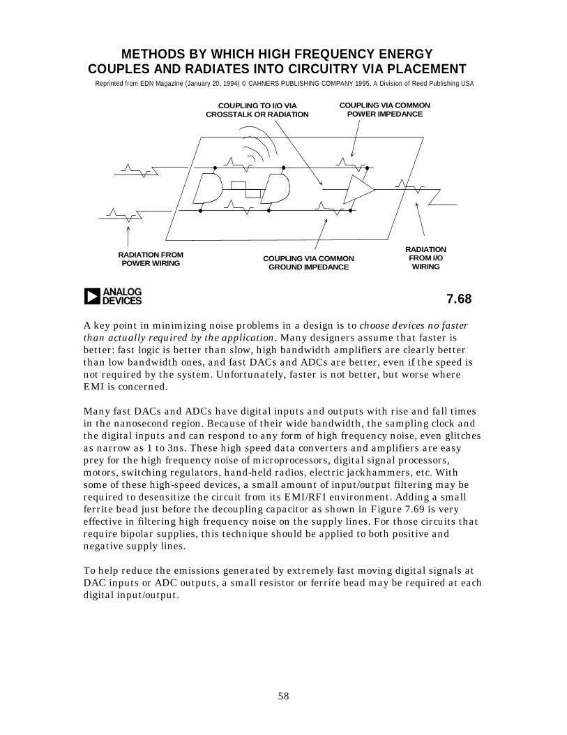
58
METHODS BY WHICH HIGH FREQUENCY ENERGYCOUPLES AND RADIATES INTO CIRCUITRY VIA PLACEMENT
7.68a
Reprinted from EDN Magazine (January 20, 1994) © CAHNERS PUBLISHING COMPANY 1995, A Division of Reed Publishing USA
COUPLING TO I/O VIACROSSTALK OR RADIATION
COUPLING VIA COMMONPOWER IMPEDANCE
COUPLING VIA COMMONGROUND IMPEDANCE
RADIATION FROMPOWER WIRING
RADIATIONFROM I/OWIRING
A key point in minimizing noise problems in a design is to choose devices no fasterthan actually required by the application. Many designers assume that faster isbetter: fast logic is better than slow, high bandwidth amplifiers are clearly betterthan low bandwidth ones, and fast DACs and ADCs are better, even if the speed isnot required by the system. Unfortunately, faster is not better, but worse whereEMI is concerned.
Many fast DACs and ADCs have digital inputs and outputs with rise and fall timesin the nanosecond region. Because of their wide bandwidth, the sampling clock andthe digital inputs and can respond to any form of high frequency noise, even glitchesas narrow as 1 to 3ns. These high speed data converters and amplifiers are easyprey for the high frequency noise of microprocessors, digital signal processors,motors, switching regulators, hand-held radios, electric jackhammers, etc. Withsome of these high-speed devices, a small amount of input/output filtering may berequired to desensitize the circuit from its EMI/RFI environment. Adding a smallferrite bead just before the decoupling capacitor as shown in Figure 7.69 is veryeffective in filtering high frequency noise on the supply lines. For those circuits thatrequire bipolar supplies, this technique should be applied to both positive andnegative supply lines.
To help reduce the emissions generated by extremely fast moving digital signals atDAC inputs or ADC outputs, a small resistor or ferrite bead may be required at eachdigital input/output.
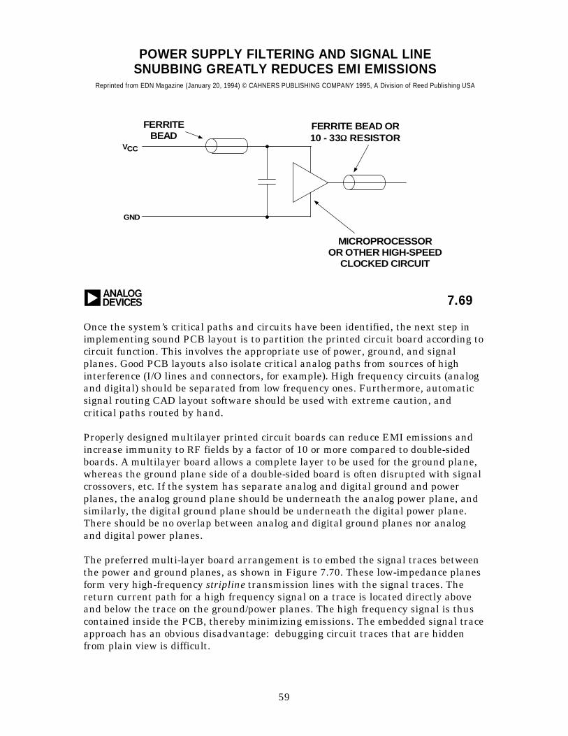
59
POWER SUPPLY FILTERING AND SIGNAL LINESNUBBING GREATLY REDUCES EMI EMISSIONS
7.69a
Reprinted from EDN Magazine (January 20, 1994) © CAHNERS PUBLISHING COMPANY 1995, A Division of Reed Publishing USA
FERRITEBEAD
GND
VCC
MICROPROCESSOROR OTHER HIGH-SPEED
CLOCKED CIRCUIT
FERRITE BEAD OR10 - 33ΩΩ RESISTOR
Once the system’s critical paths and circuits have been identified, the next step inimplementing sound PCB layout is to partition the printed circuit board according tocircuit function. This involves the appropriate use of power, ground, and signalplanes. Good PCB layouts also isolate critical analog paths from sources of highinterference (I/O lines and connectors, for example). High frequency circuits (analogand digital) should be separated from low frequency ones. Furthermore, automaticsignal routing CAD layout software should be used with extreme caution, andcritical paths routed by hand.
Properly designed multilayer printed circuit boards can reduce EMI emissions andincrease immunity to RF fields by a factor of 10 or more compared to double-sidedboards. A multilayer board allows a complete layer to be used for the ground plane,whereas the ground plane side of a double-sided board is often disrupted with signalcrossovers, etc. If the system has separate analog and digital ground and powerplanes, the analog ground plane should be underneath the analog power plane, andsimilarly, the digital ground plane should be underneath the digital power plane.There should be no overlap between analog and digital ground planes nor analogand digital power planes.
The preferred multi-layer board arrangement is to embed the signal traces betweenthe power and ground planes, as shown in Figure 7.70. These low-impedance planesform very high-frequency stripline transmission lines with the signal traces. Thereturn current path for a high frequency signal on a trace is located directly aboveand below the trace on the ground/power planes. The high frequency signal is thuscontained inside the PCB, thereby minimizing emissions. The embedded signal traceapproach has an obvious disadvantage: debugging circuit traces that are hiddenfrom plain view is difficult.
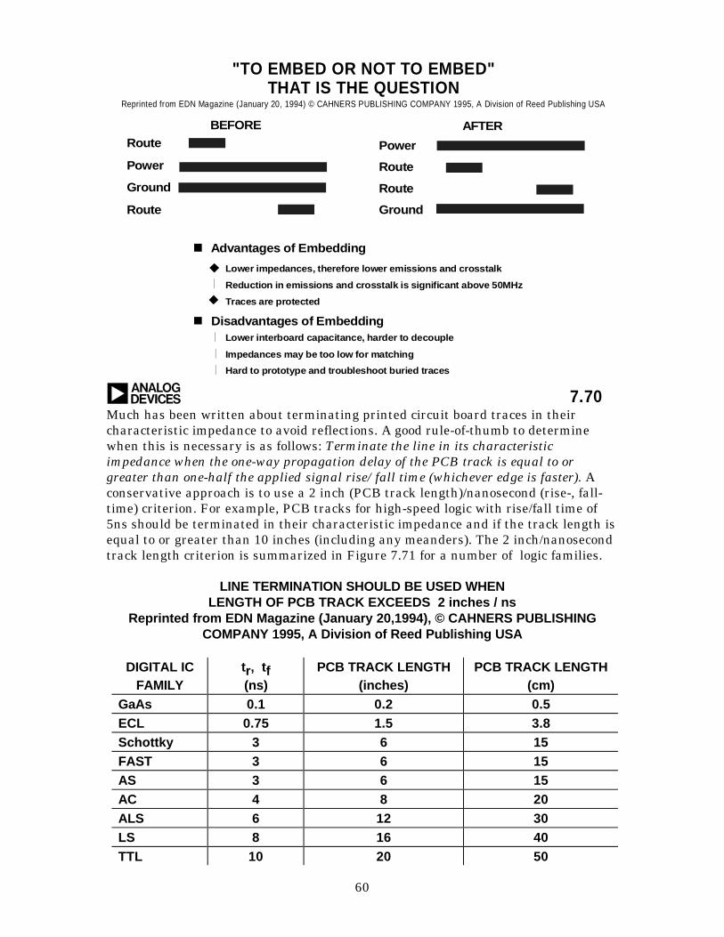
60
"TO EMBED OR NOT TO EMBED"THAT IS THE QUESTION
7.70a
Reprinted from EDN Magazine (January 20, 1994) © CAHNERS PUBLISHING COMPANY 1995, A Division of Reed Publishing USA
BEFORE AFTERRoute
Power
Ground
Route
Power
Route
Route
Ground
Advantages of Embedding
Disadvantages of Embedding
Lower impedances, therefore lower emissions and crosstalk
Reduction in emissions and crosstalk is significant above 50MHz
Traces are protected
Lower interboard capacitance, harder to decouple
Impedances may be too low for matching
Hard to prototype and troubleshoot buried traces
Much has been written about terminating printed circuit board traces in theircharacteristic impedance to avoid reflections. A good rule-of-thumb to determinewhen this is necessary is as follows: Terminate the line in its characteristicimpedance when the one-way propagation delay of the PCB track is equal to orgreater than one-half the applied signal rise/fall time (whichever edge is faster). Aconservative approach is to use a 2 inch (PCB track length)/nanosecond (rise-, fall-time) criterion. For example, PCB tracks for high-speed logic with rise/fall time of5ns should be terminated in their characteristic impedance and if the track length isequal to or greater than 10 inches (including any meanders). The 2 inch/nanosecondtrack length criterion is summarized in Figure 7.71 for a number of logic families.
LINE TERMINATION SHOULD BE USED WHENLENGTH OF PCB TRACK EXCEEDS 2 inches / ns
Reprinted from EDN Magazine (January 20,1994), © CAHNERS PUBLISHINGCOMPANY 1995, A Division of Reed Publishing USA
DIGITAL ICFAMILY
tr, tf(ns)
PCB TRACK LENGTH(inches)
PCB TRACK LENGTH(cm)
GaAs 0.1 0.2 0.5ECL 0.75 1.5 3.8Schottky 3 6 15FAST 3 6 15AS 3 6 15AC 4 8 20ALS 6 12 30LS 8 16 40TTL 10 20 50
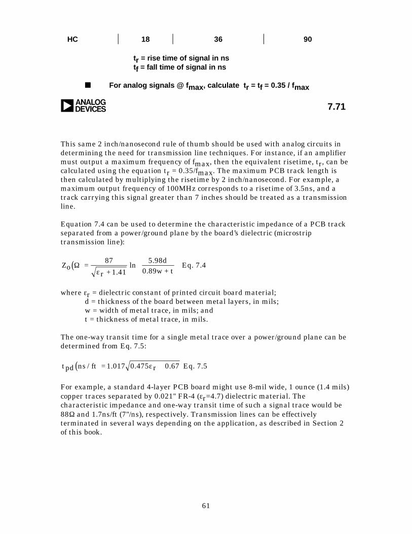
61
HC 18 36 90
tr = rise time of signal in nstf = fall time of signal in ns
nn For analog signals @ fmax, calculate tr = tf = 0.35 / fmax
a 7.71
This same 2 inch/nanosecond rule of thumb should be used with analog circuits indetermining the need for transmission line techniques. For instance, if an amplifiermust output a maximum frequency of fmax, then the equivalent risetime, tr, can becalculated using the equation tr = 0.35/fmax. The maximum PCB track length isthen calculated by multiplying the risetime by 2 inch/nanosecond. For example, amaximum output frequency of 100MHz corresponds to a risetime of 3.5ns, and atrack carrying this signal greater than 7 inches should be treated as a transmissionline.
Equation 7.4 can be used to determine the characteristic impedance of a PCB trackseparated from a power/ground plane by the board’s dielectric (microstriptransmission line):
( )Zor +1.41
5.98d0.89w + t
Ω =
87
εln Eq. 7.4
where εr = dielectric constant of printed circuit board material;d = thickness of the board between metal layers, in mils;w = width of metal trace, in mils; andt = thickness of metal trace, in mils.
The one-way transit time for a single metal trace over a power/ground plane can bedetermined from Eq. 7.5:
( )tpd ns / ft 1.017 0.475 r 0.67 = +ε Eq. 7.5
For example, a standard 4-layer PCB board might use 8-mil wide, 1 ounce (1.4 mils)copper traces separated by 0.021" FR-4 (εr=4.7) dielectric material. Thecharacteristic impedance and one-way transit time of such a signal trace would be88Ω and 1.7ns/ft (7"/ns), respectively. Transmission lines can be effectivelyterminated in several ways depending on the application, as described in Section 2of this book.
62
REFERENCES ON EMI/RFI
1. EDN’s Designer’s Guide to Electromagnetic Compatibility, EDN,January, 20, 1994, material reprinted by permission of Cahners Publishing Company, 1995.
2. Designing for EMC (Workshop Notes), Kimmel Gerke Associates, Ltd., 1994.
3. Systems Application Guide, Chapter 1, pg. 21-55, Analog Devices, Incorporated, Norwood, MA, 1994.
4. Henry Ott, Noise Reduction Techniques In Electronic Systems,Second Edition, New York, John Wiley & Sons, 1988.
5. Ralph Morrison, Grounding And Shielding Techniques In Instrumentation, Third Edition, New York, John Wiley & Sons, 1986.
6. Amplifier Applications Guide, Chapter XI, pg. 61, Analog Devices, Incorporated, Norwood, MA, 1992.
7. B.Slattery and J.Wynne, Design and Layout of a Video GraphicsSystem for Reduced EMI, Analog Devices Application Note AN-333.
8. Paul Brokaw, An IC Amplifier User Guide To Decoupling, Grounding,And Making Things Go Right For A Change, Analog DevicesApplication Note, Order Number E1393-5-590.
9. A. Rich, Understanding Interference-Type Noise, Analog Dialogue, 16-3, 1982, pp. 16-19.
10. A. Rich, Shielding and Guarding, Analog Dialogue, 17-1, 1983, pp. 8-13.
11. EMC Test & Design, Cardiff Publishing Company, Englewood, CO.An excellent, general purpose trade journal on issues of EMI and EMC.
63
SHIELDING CONCEPTS
Adolfo Garcia, John McDonald
The concepts of shielding effectiveness presented next are background material.Interested readers should consult References 1,2, and 6 cited at the end of thesection for more detailed information.
Applying the concepts of shielding requires an understanding of the source of theinterference, the environment surrounding the source, and the distance between thesource and point of observation (the receptor or victim). If the circuit is operatingclose to the source (in the near-, or induction-field), then the field characteristics aredetermined by the source. If the circuit is remotely located (in the far-, or radiation-field), then the field characteristics are determined by the transmission medium.
A circuit operates in a near-field if its distance from the source of the interference isless than the wavelength (λ) of the interference divided by 2π, or λ/2π. If the distancebetween the circuit and the source of the interference is larger than this quantity,then the circuit operates in the far field. For instance, the interference caused by a1ns pulse edge has an upper bandwidth of approximately 350MHz. The wavelengthof a 350MHz signal is approximately 32 inches (the speed of light is approximately12"/ns). Dividing the wavelength by 2π yields a distance of approximately 5 inches,the boundary between near- and far-field. If a circuit is within 5 inches of a 350MHzinterference source, then the circuit operates in the near-field of the interference. Ifthe distance is greater than 5 inches, the circuit operates in the far-field of theinterference.
Regardless of the type of interference, there is a characteristic impedance associatedwith it. The characteristic, or wave impedance of a field is determined by the ratio ofits electric (or E-) field to its magnetic (or H-) field. In the far field, the ratio of theelectric field to the magnetic field is the characteristic (wave impedance) of freespace, given by Zo = 377Ω. In the near field, the wave-impedance is determined bythe nature of the interference and its distance from the source. If the interferencesource is high-current and low-voltage (for example, a loop antenna or a power-linetransformer), the field is predominately magnetic and exhibits a wave impedancewhich is less than 377Ω. If the source is low-current and high-voltage (for example, arod antenna or a high-speed digital switching circuit), then the field ispredominately electric and exhibits a wave impedance which is greater than 377Ω.
Conductive enclosures can be used to shield sensitive circuits from the effects ofthese external fields. These materials present an impedance mismatch to theincident interference because the impedance of the shield is lower than the waveimpedance of the incident field. The effectiveness of the conductive shield depends ontwo things: First is the loss due to the reflection of the incident wave off theshielding material. Second is the loss due to the absorption of the transmitted wavewithin the shielding material. Both concepts are illustrated in Figure 7.72. Theamount of reflection loss depends upon the type of interference and its waveimpedance. The amount of absorption loss, however, is independent of the type ofinterference. It is the same for near- and far-field radiation, as well as for electric ormagnetic fields.
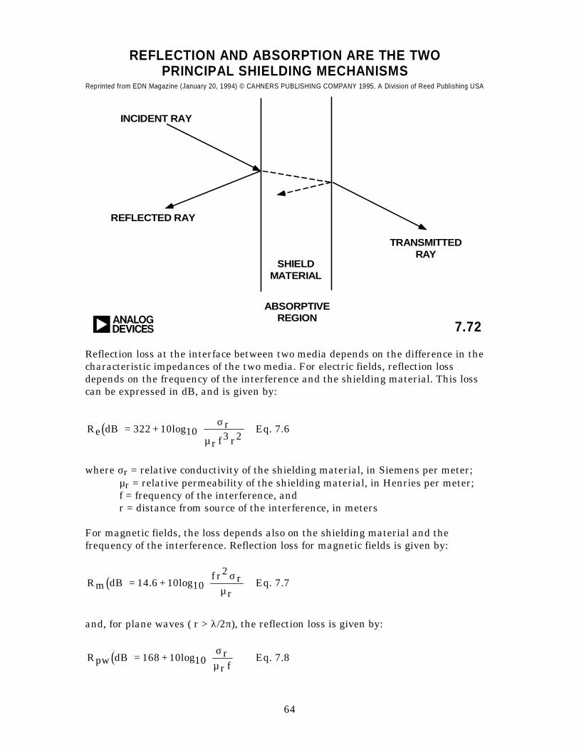
64
REFLECTION AND ABSORPTION ARE THE TWOPRINCIPAL SHIELDING MECHANISMS
7.72a
Reprinted from EDN Magazine (January 20, 1994) © CAHNERS PUBLISHING COMPANY 1995, A Division of Reed Publishing USA
INCIDENT RAY
REFLECTED RAY
ABSORPTIVEREGION
SHIELDMATERIAL
TRANSMITTEDRAY
Reflection loss at the interface between two media depends on the difference in thecharacteristic impedances of the two media. For electric fields, reflection lossdepends on the frequency of the interference and the shielding material. This losscan be expressed in dB, and is given by:
( )Re dB = 322 +10log10r
r f 3 r2σ
µ
Eq. 7.6
where σr = relative conductivity of the shielding material, in Siemens per meter;µr = relative permeability of the shielding material, in Henries per meter;f = frequency of the interference, andr = distance from source of the interference, in meters
For magnetic fields, the loss depends also on the shielding material and thefrequency of the interference. Reflection loss for magnetic fields is given by:
( )Rm dB = 14.6 +10log10f r2
rr
σµ
Eq. 7.7
and, for plane waves ( r > λ/2π), the reflection loss is given by:
( )Rpw dB = 168 +10log10rr f
σµ
Eq. 7.8
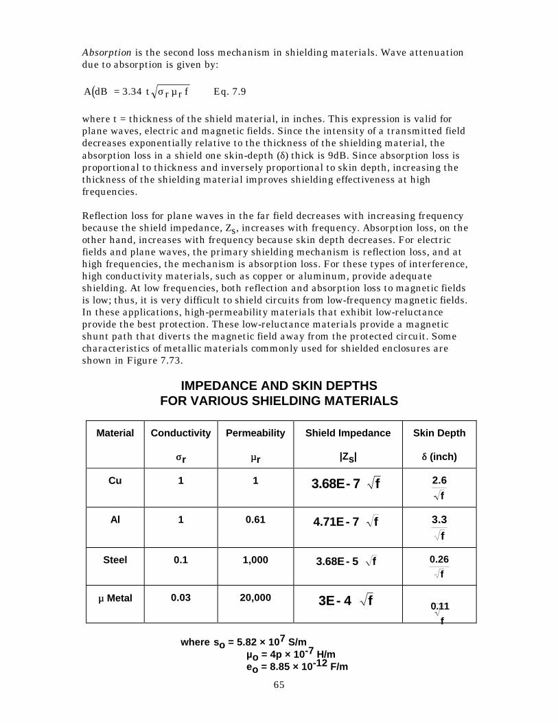
65
Absorption is the second loss mechanism in shielding materials. Wave attenuationdue to absorption is given by:
( )A dB = 3.34 t r r fσ µ Eq. 7.9
where t = thickness of the shield material, in inches. This expression is valid forplane waves, electric and magnetic fields. Since the intensity of a transmitted fielddecreases exponentially relative to the thickness of the shielding material, theabsorption loss in a shield one skin-depth (δ) thick is 9dB. Since absorption loss isproportional to thickness and inversely proportional to skin depth, increasing thethickness of the shielding material improves shielding effectiveness at highfrequencies.
Reflection loss for plane waves in the far field decreases with increasing frequencybecause the shield impedance, Zs, increases with frequency. Absorption loss, on theother hand, increases with frequency because skin depth decreases. For electricfields and plane waves, the primary shielding mechanism is reflection loss, and athigh frequencies, the mechanism is absorption loss. For these types of interference,high conductivity materials, such as copper or aluminum, provide adequateshielding. At low frequencies, both reflection and absorption loss to magnetic fieldsis low; thus, it is very difficult to shield circuits from low-frequency magnetic fields.In these applications, high-permeability materials that exhibit low-reluctanceprovide the best protection. These low-reluctance materials provide a magneticshunt path that diverts the magnetic field away from the protected circuit. Somecharacteristics of metallic materials commonly used for shielded enclosures areshown in Figure 7.73.
IMPEDANCE AND SKIN DEPTHSFOR VARIOUS SHIELDING MATERIALS
Material Conductivity
σσr
Permeability
µµr
Shield Impedance
|Zs|
Skin Depth
δδ (inch)
Cu 1 1 3.68E- 7 f ⋅⋅ 2.6
f
Al 1 0.61 4.71E- 7 f ⋅⋅ 3.3
f
Steel 0.1 1,000 3.68E- 5 f ⋅⋅ 0.26
f
µµ Metal 0.03 20,000 3E- 4 f ⋅⋅ 0.11
f
where so = 5.82 × 10⁷ S/mµo = 4p × 10-7 H/meo = 8.85 × 10⁻¹² F/m
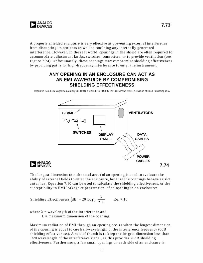
66
a 7.73
A properly shielded enclosure is very effective at preventing external interferencefrom disrupting its contents as well as confining any internally-generatedinterference. However, in the real world, openings in the shield are often required toaccommodate adjustment knobs, switches, connectors, or to provide ventilation (seeFigure 7.74). Unfortunately, these openings may compromise shielding effectivenessby providing paths for high-frequency interference to enter the instrument.
ANY OPENING IN AN ENCLOSURE CAN ACT ASAN EMI WAVEGUIDE BY COMPROMISING
SHIELDING EFFECTIVENESS
7.74a
Reprinted from EDN Magazine (January 20, 1994) © CAHNERS PUBLISHING COMPANY 1995, A Division of Reed Publishing USA
SEAMS
SWITCHESDISPLAYPANEL
DATACABLES
POWERCABLES
VENTILATORS
The longest dimension (not the total area) of an opening is used to evaluate theability of external fields to enter the enclosure, because the openings behave as slotantennas. Equation 7.10 can be used to calculate the shielding effectiveness, or thesusceptibility to EMI leakage or penetration, of an opening in an enclosure:
( )Shielding Effectiveness dB = 20 log10 2 Lλ⋅
Eq. 7.10
where λ = wavelength of the interference andL = maximum dimension of the opening
Maximum radiation of EMI through an opening occurs when the longest dimensionof the opening is equal to one half-wavelength of the interference frequency (0dBshielding effectiveness). A rule-of-thumb is to keep the longest dimension less than1/20 wavelength of the interference signal, as this provides 20dB shieldingeffectiveness. Furthermore, a few small openings on each side of an enclosure is
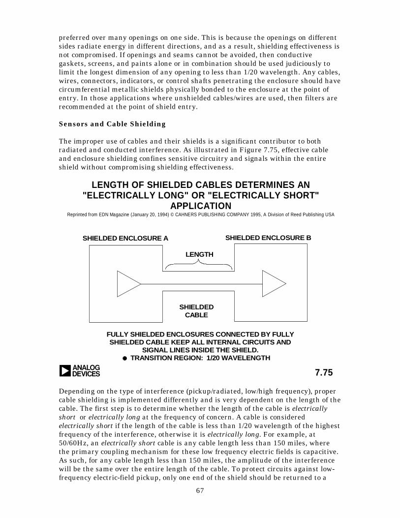
67
preferred over many openings on one side. This is because the openings on differentsides radiate energy in different directions, and as a result, shielding effectiveness isnot compromised. If openings and seams cannot be avoided, then conductivegaskets, screens, and paints alone or in combination should be used judiciously tolimit the longest dimension of any opening to less than 1/20 wavelength. Any cables,wires, connectors, indicators, or control shafts penetrating the enclosure should havecircumferential metallic shields physically bonded to the enclosure at the point ofentry. In those applications where unshielded cables/wires are used, then filters arerecommended at the point of shield entry.
Sensors and Cable Shielding
The improper use of cables and their shields is a significant contributor to bothradiated and conducted interference. As illustrated in Figure 7.75, effective cableand enclosure shielding confines sensitive circuitry and signals within the entireshield without compromising shielding effectiveness.
LENGTH OF SHIELDED CABLES DETERMINES AN"ELECTRICALLY LONG" OR "ELECTRICALLY SHORT"
APPLICATION
7.75a
Reprinted from EDN Magazine (January 20, 1994) © CAHNERS PUBLISHING COMPANY 1995, A Division of Reed Publishing USA
SHIELDED ENCLOSURE A SHIELDED ENCLOSURE B
LENGTH
SHIELDEDCABLE
FULLY SHIELDED ENCLOSURES CONNECTED BY FULLYSHIELDED CABLE KEEP ALL INTERNAL CIRCUITS AND
SIGNAL LINES INSIDE THE SHIELD.TRANSITION REGION: 1/20 WAVELENGTH
Depending on the type of interference (pickup/radiated, low/high frequency), propercable shielding is implemented differently and is very dependent on the length of thecable. The first step is to determine whether the length of the cable is electricallyshort or electrically long at the frequency of concern. A cable is consideredelectrically short if the length of the cable is less than 1/20 wavelength of the highestfrequency of the interference, otherwise it is electrically long. For example, at50/60Hz, an electrically short cable is any cable length less than 150 miles, wherethe primary coupling mechanism for these low frequency electric fields is capacitive.As such, for any cable length less than 150 miles, the amplitude of the interferencewill be the same over the entire length of the cable. To protect circuits against low-frequency electric-field pickup, only one end of the shield should be returned to a
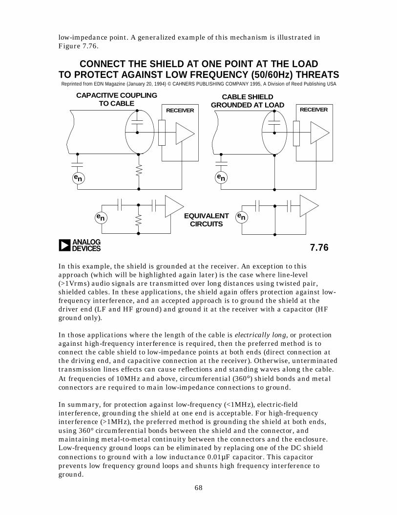
68
low-impedance point. A generalized example of this mechanism is illustrated inFigure 7.76.
CONNECT THE SHIELD AT ONE POINT AT THE LOADTO PROTECT AGAINST LOW FREQUENCY (50/60Hz) THREATS
7.76a
Reprinted from EDN Magazine (January 20, 1994) © CAHNERS PUBLISHING COMPANY 1995, A Division of Reed Publishing USA
EQUIVALENTCIRCUITS
RECEIVER RECEIVER
CABLE SHIELDGROUNDED AT LOAD
CAPACITIVE COUPLINGTO CABLE
en
en en
en
In this example, the shield is grounded at the receiver. An exception to thisapproach (which will be highlighted again later) is the case where line-level(>1Vrms) audio signals are transmitted over long distances using twisted pair,shielded cables. In these applications, the shield again offers protection against low-frequency interference, and an accepted approach is to ground the shield at thedriver end (LF and HF ground) and ground it at the receiver with a capacitor (HFground only).
In those applications where the length of the cable is electrically long, or protectionagainst high-frequency interference is required, then the preferred method is toconnect the cable shield to low-impedance points at both ends (direct connection atthe driving end, and capacitive connection at the receiver). Otherwise, unterminatedtransmission lines effects can cause reflections and standing waves along the cable.At frequencies of 10MHz and above, circumferential (360°) shield bonds and metalconnectors are required to main low-impedance connections to ground.
In summary, for protection against low-frequency (<1MHz), electric-fieldinterference, grounding the shield at one end is acceptable. For high-frequencyinterference (>1MHz), the preferred method is grounding the shield at both ends,using 360° circumferential bonds between the shield and the connector, andmaintaining metal-to-metal continuity between the connectors and the enclosure.Low-frequency ground loops can be eliminated by replacing one of the DC shieldconnections to ground with a low inductance 0.01µF capacitor. This capacitorprevents low frequency ground loops and shunts high frequency interference toground.
69
Shielded Twisted Pair Cable Grounding Examples
The environments in which analog systems operate are often rich in sources of EMI.Common EMI noise sources include power lines, logic signals, switching powersupplies, radio stations, electric lighting, and motors. Noise from these sources caneasily couple into long analog signal paths, such as cables, which act as efficientantennas. Shielded cables protect signal conductors from electric field (E-field)interference by providing low impedance paths to ground at the offendingfrequencies. Aluminum foil, copper, and braided stainless steel are materials verycommonly used for cable shields due to their low impedance properties.
Simply increasing the separation between the noise source and the cable will yieldsignificant additional attenuation due to reduced coupling, but shielding is stillrequired in most applications involving remote sensors.
There are two paths from an EMI source to a susceptible cable: capacitive (or E-field) and magnetic (or H-field) coupling. Capacitive coupling occurs when parasiticcapacitance exists between a noise source and the cable. The amount of parasiticcapacitance is determined by the separation, shape, orientation, and the mediumbetween the source and the cable.
Magnetic coupling occurs through parasitic mutual inductance when a magneticfield is coupled from one conductor to another. Parasitic mutual inductance dependson the shape and relative orientation of the circuits in question, the magneticproperties of the medium, and is directly proportional to conductor loop area.Minimizing conductor loop area reduces magnetic coupling proportionally.
Shielded twisted pair cables offer further noise immunity to magnetic fields.Twisting the conductors together reduces the net loop area, which has the effect ofcanceling any magnetic field pickup, because the sum of positive and negativeincremental loop areas is ideally equal to zero.
To study the shielding problem, a precision RTD (Resistance Temperature Detector)amplifier circuit was used as the basis for a series of experiments. A remote 100ΩRTD was connected to the bridge, bridge driver, and the bridge amplifier circuit(Figure 7.77) using 10 feet of a shielded twisted pair cable. The RTD is one elementof a 4-element bridge (the three other resistor elements are located in the bridge andbridge driver circuit). The gain of the instrumentation amplifier was adjusted sothat the sensitivity at the output was 10mV/°C, with a 5V full scale. Measurementswere made at the output of the instrumentation amplifier with the shield groundedin various ways. The experiments were conducted in lab standard environmentwhere a considerable amount of electronic equipment was in operation.
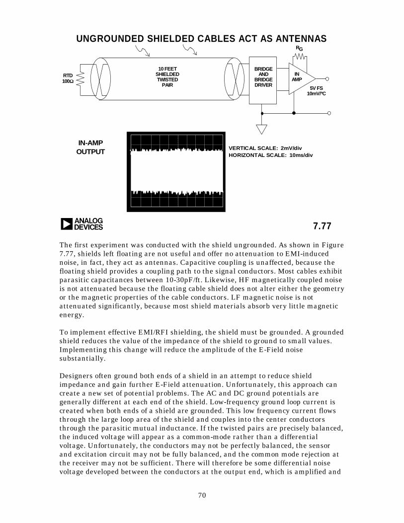
70
UNGROUNDED SHIELDED CABLES ACT AS ANTENNAS
7.77a
IN-AMPOUTPUT
VERTICAL SCALE: 2mV/divHORIZONTAL SCALE: 10ms/div
BRIDGEAND
BRIDGEDRIVER
INAMP
RG
5V FS10mV/ºC
10 FEETSHIELDEDTWISTED
PAIR
RTD100ΩΩ
The first experiment was conducted with the shield ungrounded. As shown in Figure7.77, shields left floating are not useful and offer no attenuation to EMI-inducednoise, in fact, they act as antennas. Capacitive coupling is unaffected, because thefloating shield provides a coupling path to the signal conductors. Most cables exhibitparasitic capacitances between 10-30pF/ft. Likewise, HF magnetically coupled noiseis not attenuated because the floating cable shield does not alter either the geometryor the magnetic properties of the cable conductors. LF magnetic noise is notattenuated significantly, because most shield materials absorb very little magneticenergy.
To implement effective EMI/RFI shielding, the shield must be grounded. A groundedshield reduces the value of the impedance of the shield to ground to small values.Implementing this change will reduce the amplitude of the E-Field noisesubstantially.
Designers often ground both ends of a shield in an attempt to reduce shieldimpedance and gain further E-Field attenuation. Unfortunately, this approach cancreate a new set of potential problems. The AC and DC ground potentials aregenerally different at each end of the shield. Low-frequency ground loop current iscreated when both ends of a shield are grounded. This low frequency current flowsthrough the large loop area of the shield and couples into the center conductorsthrough the parasitic mutual inductance. If the twisted pairs are precisely balanced,the induced voltage will appear as a common-mode rather than a differentialvoltage. Unfortunately, the conductors may not be perfectly balanced, the sensorand excitation circuit may not be fully balanced, and the common mode rejection atthe receiver may not be sufficient. There will therefore be some differential noisevoltage developed between the conductors at the output end, which is amplified and
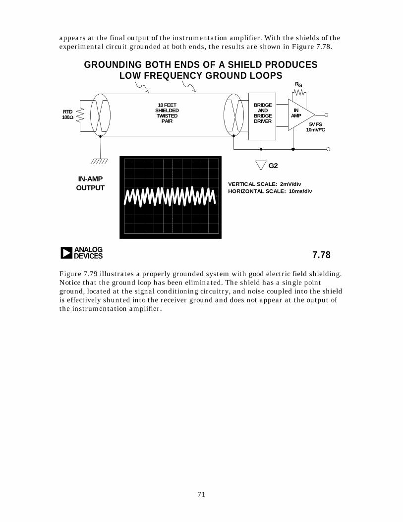
71
appears at the final output of the instrumentation amplifier. With the shields of theexperimental circuit grounded at both ends, the results are shown in Figure 7.78.
GROUNDING BOTH ENDS OF A SHIELD PRODUCESLOW FREQUENCY GROUND LOOPS
7.78a
IN-AMPOUTPUT
VERTICAL SCALE: 2mV/divHORIZONTAL SCALE: 10ms/div
BRIDGEAND
BRIDGEDRIVER
INAMP
RG
5V FS10mV/ºC
10 FEETSHIELDEDTWISTED
PAIR
RTD100ΩΩ
G2
Figure 7.79 illustrates a properly grounded system with good electric field shielding.Notice that the ground loop has been eliminated. The shield has a single pointground, located at the signal conditioning circuitry, and noise coupled into the shieldis effectively shunted into the receiver ground and does not appear at the output ofthe instrumentation amplifier.
72
GROUNDING SHIELD AT RECEIVER END SHUNTS LOW- ANDHIGH-FREQUENCY NOISE INTO RECEIVER GROUND
7.79a
IN-AMPOUTPUT
VERTICAL SCALE: 2mV/divHORIZONTAL SCALE: 10ms/div
BRIDGEAND
BRIDGEDRIVER
INAMP
RG
5V FS10mV/ºC
10 FEETSHIELDEDTWISTED
PAIR
RTD100ΩΩ
Figure 7.80 shows an example of a remotely located, ungrounded, passive sensor(ECG electrodes) which is connected to a high-gain, low power AD620instrumentation amplifier through a shielded twisted pair cable. Note that theshield is properly grounded at the signal conditioning circuitry. The AD620 gain is1000× , and the amplifier is operated on ±3V supplies. Notice the absence of 60Hzinterference in the amplifier output.
73
FOR UNGROUNDED PASSIVE SENSORS,GROUND SHIELD AT THE RECEIVING END
7.80a
IN-AMPOUTPUT
VERTICAL SCALE: 10mV/divHORIZONTAL SCALE: 0.2sec/div
AD620
RG
SHIELDEDTWISTED
PAIR
G1
+
-
REF OUTPUT
G = 1000
G2
EEGELECTRODES
+
-
Most high impedance sensors generate low-level current or voltage outputs, such asa photodiode responding to incident light. These low-level signals are especiallysusceptible to EMI, and often are of the same order of magnitude as the parasiticparameters of the cable and input amplifier.
Even properly shielded cables can degrade the signals by introducing parasiticcapacitance that limits bandwidth, and leakage currents that limit sensitivity. Anexample is shown in Figure 7.81, where a high-impedance photodiode is connected toa preamp through a long shielded twisted pair cable. Not only will the cablecapacitance limit bandwidth, but cable leakage current limits sensitivity. A pre-amplifier, located close to the high-impedance sensor, is recommended to amplify thesignal and to minimize the effect of cable parasitics.
74
SHIELDS ARE NOT EFFECTIVE WITHHIGH IMPEDANCE REMOTE SENSORS
7.81a
CCOMP
SHIELDEDTWISTED
PAIR +
-
PHOTODIODEDETECTOR RFB
HIGHIMPEDANCE>100MΩΩ ≈≈ 20pF/ft
CABLE CAPACITANCE LIMITS BANDWIDTH
CABLE LEAKAGE CURRENT LIMITS SENSITIVITY
Figure 7.82 is an example of a high-impedance photodiode detector and pre-amplifier, driving a shielded twisted pair cable. Both the amplifier and the shield aregrounded at a remote location. The shield is connected to the cable driver common,G1, ensuring that the signal and the shield at the driving end are both referenced tothe same point. The capacitor on the receiving side of the cable shunts highfrequency noise on the shield into ground G2 without introducing a low-frequencyground loop. This popular grounding scheme is known as hybrid grounding.

75
REMOTELY LOCATED HIGH IMPEDANCESENSOR WITH PREAMP
7.82a
REF
IN-AMPSHIELDEDTWISTED
PAIR
PHOTODIODEPREAMP
-
+
G2
HF GROUND
RG
G1
LF AND HFGROUND
-
+
Figure 7.83 illustrates a balanced active line driver with a hybrid shield groundimplementation. When a system’s operation calls for a wide frequency range, thehybrid grounding technique often provides the best choice (Reference 8). Thecapacitor at the receiving end shunts high-frequency noise on the shield into G2without introducing a low-frequency ground loop. At the receiver, a common-modechoke can be used to help prevent RF pickup entering the receiver, and subsequentRFI rectification (see References 9 and 10). Care should be taken that the shieldsare grounded to the chassis entry points to prevent contamination of the signalground (Reference 11).
76
HYBRID (LF AND HF) GROUNDING WITH ACTIVE DRIVER
7.83a
REF
SHIELDEDTWISTED
PAIR
-
G2
HF GROUND
G1
LF AND HFGROUND
BALANCEDLINEDRIVER
BALANCEDLINERECEIVER
CMCHOKE
To summarize this discussion, shield grounding techniques must take into accountthe type and the configuration of the sensor as well as the nature of the interference.When a low-impedance passive sensor is used, grounding the shield to the receivingend is the best choice. Active sensor shields should generally be grounded at thesource (direct connection to source ground) and at the receiver (connect to receiverground using a capacitor). This hybrid approach minimizes high-frequencyinterference and prevents low-frequency ground loops. Shielded twisted conductorsoffer additional protection against shield noise because the coupled noise occurs as acommon-mode, and not a differential signal.
The best shield can be compromised by poor connection techniques. Shields often use“pig-tail” connections to make the connection to ground. A “pig-tail” connection is asingle wire connection from shield to either chassis or circuit ground. This type ofconnection is inexpensive, but at high frequency, it does not provide low impedance.Quality shields do not leave large gaps in the cable/instrument shielding system.Shield gaps provide paths for high frequency EMI to enter the system. The cableshielding system should include the cable end connectors. Ideally, cable shieldconnectors should make 360° contact with the chassis ground.
As shown in Figure 7.84, pigtail terminations on cables very often cause systems tofail radiated emissions tests because high-frequency noise has coupled into the cableshield, generally through stray capacitance. If the length of the cable is consideredelectrically long at the interference frequency, then it can behave as a very efficientquarter-wave antenna. The cable pigtail forms a matching network, as shown in thefigure, to radiate the noise which coupled into the shield. In general, pigtails areonly recommended for applications below 10kHz, such as 50/60Hz interferenceprotection. For applications where the interference is greater than 10kHz, shieldedconnectors, electrically and physically connected to the chassis, should be used.
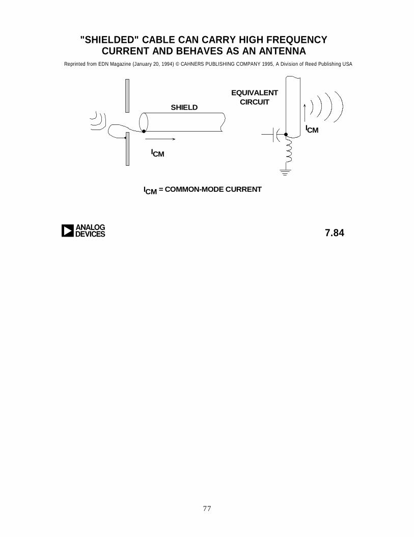
77
"SHIELDED" CABLE CAN CARRY HIGH FREQUENCYCURRENT AND BEHAVES AS AN ANTENNA
7.84a
Reprinted from EDN Magazine (January 20, 1994) © CAHNERS PUBLISHING COMPANY 1995, A Division of Reed Publishing USA
ICM
ICM
ICM = COMMON-MODE CURRENT
SHIELD
EQUIVALENTCIRCUIT
78
REFERENCES: CABLE SHIELDING
1. H.W. Ott, Noise Reduction Techniques in Electronic Systems,Second Edition, John Wiley & Sons, Inc., New York, 1988.
2. Ralph Morrison, Grounding and Shielding Techniques inInstrumentation, Third Edition, John Wiley & Sons, Inc.,New York, 1988.
3. Systems Application Guide, Section 1, Analog Devices, Inc.,Norwood, MA, 1993.
4. AD620 Instrumentation Amplifier, Data Sheet, Analog Devices, Inc.
5. A. Rich, Understanding Interference-Type Noise, Analog Dialogue,16-3, 1982, pp. 16-19.
6. A. Rich, Shielding and Guarding, Analog Dialogue, 17-1, 1983,pp. 8-13.
7. EDN’s Designer’s Guide to Electromagnetic Compatibility, EDN,January, 20, 1994, material reprinted by permission of CahnersPublishing Company, 1995.
8. Designing for EMC (Workshop Notes), Kimmel Gerke Associates,Ltd., 1994.
9. James Bryant and Herman Gelbach, High Frequency SignalContamination, Analog Dialogue, Vol. 27-2, 1993.
10. Walt Jung, System RF Interference Prevention, Analog Dialogue,Vol. 28-2, 1994.
11. Neil Muncy, Noise Susceptibility in Analog and Digital SignalProcessing Systems, presented at 97th Audio Engineering SocietyConvention, Nov. 1994.
79
GENERAL REFERENCES: HARDWAREDESIGN TECHNIQUES
1. Linear Design Seminar, Section 11, Analog Devices, Inc., 1995.
2. E.S.D. Prevention Manual Available free from Analog Devices, Inc.
3. B.I. & B. Bleaney, Electricity & Magnetism, OUP 1957, pp 23,24, & 52.
4. Paul Brokaw, An I.C. Amplifier User's Guide to Decoupling, Groundingand Making Things Go Right for a Change, Analog Devices Application Note, Available free of charge from Analog Devices, Inc.
5. Jeff Barrow, Avoiding Ground Problems in High Speed Circuits,R.F. Design, July 1989.
AND
Paul Brokaw & Jeff Barrow, Grounding for Low- and High-Frequency Circuits, Analog Dialogue, 23-3 1989.
Free from Analog Devices.
6. International EMI Emission Regulations Canada CSA C108.8-M1983 FDR VDE 0871/VDE 0875 Japan CISPR (VCCI)/PUB 22 USA FCC-15 Part J
7. Bill Slattery & John Wynne, Design & Layout of a Video Graphics Systemfor Reduced EMI, Analog Devices Application Note (E1309-15-10/89)
Free from Analog Devices.
8. William R. Blood, Jr., MECL System Design Handbook(HB205, Rev. 1), Motorola Semiconductor Products, Inc., 1988.
9. Wainwright Instruments Inc., 69 Madison Ave., Telford, PA,18969-1829, Tel. 215-723-4333, Fax. 215-723-4620.
Wainwright Instruments GmbH, Widdersberger Strasse 14,DW-8138 Andechs-Frieding, Germany. Tel: +49-8152-3162,Fax: +49-8152-40525.
10. Ralph Morrison, Grounding and Shielding Techniques in Instrumentation, Third Edition, John Wiley, Inc., 1986.
11. Henry W. Ott, Noise Reduction Techniques in Electronic Systems, Second Edition, John Wiley, Inc., 1988.
12. Robert A. Pease, Troubleshooting Analog Circuits, Butterworth-Heinemann, 1991.
80
13. Jim Williams, Editor, Analog Circuit Design: Art, Science, and Personalities, Butterworth-Heinemann, 1991.
14. Doug Grant and Scott Wurcer, Avoiding Passive Component Pitfalls,The Best of Analog Dialogue, pp. 143-148, Analog Devices, Inc., 1991.
15. Walt Jung and Richard Marsh, Picking Capacitors, Part I., Audio,February, 1980.
16. Walt Jung and Richard Marsh, Picking Capacitors, Part II., Audio,March, 1980.
17. Daryl Gerke and Bill Kimmel, The Designer's Guide to Electromagnetic Compatibility, EDN Supplement, January 20, 1994.
18. Walt Kester, Basic Characteristics Distinguish Sampling A/D Converters,EDN, September 3, 1992, pp.135-144.
19. Walt Kester, Peripheral Circuits Can Make or Break Sampling ADCSystem, EDN, October 1, 1992, pp. 97-105.
20. Walt Kester, Layout, Grounding, and Filtering Complete SamplingADC System, EDN, October 15, 1992, pp. 127-134.
21. Howard W. Johnson and Martin Graham, High-Speed Digital Design,PTR Prentice Hall, 1993.