greenchip tea1755 integrated pfc and flyback controller greenchip tea1755 integrated pfc and flyback...
TRANSCRIPT
AN11142GreenChip TEA1755 integrated PFC and flyback controllerRev. 2 — 13 September 2017 Application note
COMPANY PUBLIC
Document informationInformation ContentKeywords GreenChip, TEA1755, PFC, flyback, high-efficiency, adapter, notebook, PC
power, low-power standby mode
Abstract The TEA1755 is a member of the new generation of combined PFC andflyback controller ICs, used for efficient switched mode power supplies. Burstmode enhances the overall efficiency of the system at low-output power andimproves the audible noise performance. The TEA1755 has a high levelof integration allowing cost-effective design of power supplies using theminimum number of external components. The TEA1755 is fabricated in aSilicon-On-Insulator (SOI) process, enabling it to operate at a wide voltagerange.

NXP Semiconductors AN11142GreenChip TEA1755 integrated PFC and flyback controller
AN11142 All information provided in this document is subject to legal disclaimers. © NXP B.V. 2017. All rights reserved.
Application note Rev. 2 — 13 September 2017COMPANY PUBLIC 2 / 56
Revision historyRev Date Descriptionv.2 20170912 second, updated version
Modifications: • Text and graphics have been updated throughout the document.
v.1 20121112 first issue

NXP Semiconductors AN11142GreenChip TEA1755 integrated PFC and flyback controller
AN11142 All information provided in this document is subject to legal disclaimers. © NXP B.V. 2017. All rights reserved.
Application note Rev. 2 — 13 September 2017COMPANY PUBLIC 3 / 56
1 Introduction
The TEA1755 is a combination controller comprising an integrated PFC and flybackcontroller in an SO16 package. Both controllers operate in Quasi-Resonant (QR)mode and in Discontinuous Conduction Mode (DCM) with valley detection and areindependently switched.
The PFC output power is on-time controlled for simplicity. It is not necessary to sensethe phase of the mains voltage. The flyback output power is current mode controlledproviding good input voltage ripple suppression.
The integrated communication circuitry between the controllers does not requireadjustment.
Note: The voltage and current levels contained in this application note are typical values.The specification of the pin level spreading is given in the TEA1755T and TEA1755LTdata sheets.
Note: In all cases where a parameter value in this application note is different from thesame parameter in the data sheet, the data sheet is leading.
1.1 ScopeThis application note describes the functionality of the TEA1755 and the adjustmentsrequired within the power converter application.
Excluded from this document are the large signal parts of the PFC/flyback power stagesand the coil/transformer design and data.
1.2 The TEA1755 GreenChip controllerThe GreenChip features allow the design of reliable, cost-effective, and efficient SwitchedMode Power Supplies (SMPS) using the minimum number of external components.
1.2.1 Key features• PFC and flyback controller integrated in one SO16 package• Switching frequencies of PFC and flyback controller are independent of each other• No external hardware required for the communication between both controllers• High level of integration, resulting in a low external component count• Integrated mains voltage enable and brownout protection• Fast-latch reset function implemented• Power-down functionality for very low Standby mode power requirements
NXP Semiconductors AN11142GreenChip TEA1755 integrated PFC and flyback controller
AN11142 All information provided in this document is subject to legal disclaimers. © NXP B.V. 2017. All rights reserved.
Application note Rev. 2 — 13 September 2017COMPANY PUBLIC 4 / 56
1.2.2 System features• Safe restart mode for system fault conditions• High-voltage start-up current source (5 mA)• Reduction of HV current source (1 mA) in safe restart mode• Wide VCC range (13.4 V to 38 V)• MOSFET driver voltage limited• Easy control of start-up behavior and VCC circuit• General-purpose input for latched protection• Internal IC overtemperature protection• Accurate PFC switch on/switch off control using flyback switching frequency
measurement• One high-voltage spacer between the HV pin and the next active pin• Open pin protection on the VINSENSE, VOSENSE, PFCAUX, FBCTRL, and FBAUX
pins
1.2.3 PFC features• Dual-output voltage boost converter• QR/DCM operation with valley switching• Frequency limitation (139 kHz) to reduce switching losses and ElectroMagnetic
Interference (EMI)• ton controlled• Mains input voltage compensation for control loop for good transient response• OverCurrent Protection (OCP)• Soft-start and soft-stop• Open/short-circuit detection for PFC feedback loop: no external OverVoltage Protection
(OVP) circuit necessary• Adjustable delay for switching off the PFC• Overriding the PFC switch on/switch off functionality
1.2.4 Flyback features• Burst/FR/QR/DCM operation with valley switching• Frequency Reduction (FR) with an adjustable minimum peak current and valley
switching to maintain high efficiency at low output power levels• Burst mode enhances the overall efficiency at low-output power• Burst mode benefits the reduction of audible noise• Frequency limitation (130 kHz) to reduce switching losses and EMI• Current mode controlled• Overcurrent protection• Soft-start• Accurate OVP through auxiliary winding• Time-out protection for output overloads and open feedback loop, available as safe
restart (TEA1755T) or latched (TEA1755LT) protection• VCC undervoltage prevention during burst mode
NXP Semiconductors AN11142GreenChip TEA1755 integrated PFC and flyback controller
AN11142 All information provided in this document is subject to legal disclaimers. © NXP B.V. 2017. All rights reserved.
Application note Rev. 2 — 13 September 2017COMPANY PUBLIC 5 / 56
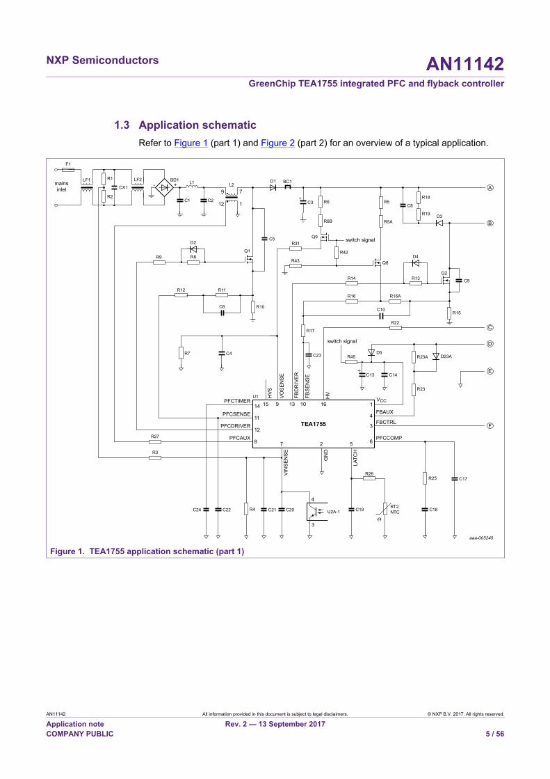
1.3 Application schematicRefer to Figure 1 (part 1) and Figure 2 (part 2) for an overview of a typical application.
+mainsinlet
C17
C18C19
U1PFCTIMER
GN
D
LATC
H
VIN
SEN
SE
HVS
VO
SE
NS
E
FBD
RIV
ER
FBS
ENS
E
HV
VCC
PFCSENSE
PFCDRIVER
PFCAUX
C20C21C22C24 R4
R25R26
RT2NTC
C14
C10
C23C4R7
R10C6
R11
R27
R3
R12
R9
C5
C2C1
BD1LF2LF1
F1
CX1
R1
R2
D1 BC1
R14
R31
R43
R42
R13
D4
D3
Q2
R18
R19
R15
R17
R6B
R6
R5A
Q8
Q9
R5
R16 R16A
Q1R8
D2
7
1
9
12
TEA1755
C13
FBCTRL
FBAUX
PFCCOMP
R23A
R23
D23AD5
R22
R45
C9
C8C3
L2L1
4
14
11
12
8 7
15 9 13 10 16 1
2 5
3
6
aaa-005245
- A
B
C
D
E
F
U2A-1
4
3
switch signal
switch signal
Figure 1. TEA1755 application schematic (part 1)

NXP Semiconductors AN11142GreenChip TEA1755 integrated PFC and flyback controller
AN11142 All information provided in this document is subject to legal disclaimers. © NXP B.V. 2017. All rights reserved.
Application note Rev. 2 — 13 September 2017COMPANY PUBLIC 6 / 56
T1
5
1
4
2
6
019aab986
CY1 BC2
U3VCC
C30
R30
Q4
R32
R33 C31
D30113
4
2
5
DR
IVE
R
SR
SEN
SE
n.c.
6 1GND
SELREG TEA1792
C53
D52
Q7
R54R52
R50
R51
R53
1
2
C15
C16
D50
C27
U2A-2
L4
C28C52C51C50
C29
L3
7, 8
9, 10
Vout+
U5VSENSE
3 1
2
6
5
4OPTO
GND
VCC
SWDET
PSENSE TEA1703
R35
R36
C34
R56
R34R37
R38
1
2U2-1
4
3
U2-2
U4
R55
C35
R24
R57
Vout-
A
B
C
D
E
F
Figure 2. TEA1755 application schematic (part 2)

NXP Semiconductors AN11142GreenChip TEA1755 integrated PFC and flyback controller
AN11142 All information provided in this document is subject to legal disclaimers. © NXP B.V. 2017. All rights reserved.
Application note Rev. 2 — 13 September 2017COMPANY PUBLIC 7 / 56
2 Pin descriptionTable 1. Pin descriptionPin Name Functional description1 VCC Supply voltage; Vstartup = 22.3 V; Vth(UVLO) = 13.4 V.
At mains switch-on, the capacitor connected to this pin is charged to Vstartupby the internal HV current source. When the VCC < 0.6 V, the chargecurrent is limited to 1.1 mA. This feature prevents overheating of the IC ifthe VCC pin is short-circuited. When the pin voltage is between 0.6 V andVth(UVLO), the charge current is 5 mA to enable a fast start-up. When it isbetween Vth(UVLO) and Vstartup, the charge current is limited to 1 mA againto reduce the safe restart duty cycle. The result is a reduction of the inputpower during fault conditions. When Vstartup is reached, the HV currentsource is pinched off and VCC is regulated to Vstartup until the flyback starts.See Section 3.2 for a complete description of the start-up sequence.
2 GND Ground connection.
3 FBCTRL Control input for flyback for direct connection of the optocoupler. At acontrol voltage of 4.9 V, the flyback delivers maximum power. The flybackenters FR mode at a control voltage of 4 V and burst mode at a control-voltage of approximately 1.2 V. It exits burst mode at 2.8 V. The flybackdriver stops switching when FBCTRL is lower than 0.77 V. The built-inlogic controls an internal 29 µA current source that is connected to the pin.This current source can be used to implement a timeout function to detectan open control loop or a short circuit of the output voltage. The timeoutfunction is disabled by connecting a resistor of 180 kΩ between this pin andground.
4 FBAUX Input from auxiliary winding for transformer demagnetization detection,mains dependent OverPower Protection (OPP), and OverVoltageProtection (OVP) of the flyback.The combination of demagnetization and the valley detection on the HV pindetermines the switch-on moment of the flyback controller in the valley. Aflyback OVP is detected at a current higher than 300 μA to the FBAUX pin.Internal filtering prevents false detection of an OVP. The flyback OPP startsat a current lower than −100 μA from the FBAUX pin.
5 LATCH General-purpose latched protection input.When Vstartup (on the VCC pin) is reached, the LATCH pin is charged to582 mV before the PFC and flyback controllers can be switched on. Thelatched protection is triggered when the pin is pulled below 494 mV and thePFC and the flyback are switched off.The logic controls an internal 30.5 µA current source which is connectedto the pin. Using this current source, an optional Negative TemperatureCoefficient (NTC) resistor can be directly connected to the LATCH pin fortemperature protection.
6 PFCCOMP Frequency compensation pin for the PFC control loop.

NXP Semiconductors AN11142GreenChip TEA1755 integrated PFC and flyback controller
AN11142 All information provided in this document is subject to legal disclaimers. © NXP B.V. 2017. All rights reserved.
Application note Rev. 2 — 13 September 2017COMPANY PUBLIC 8 / 56
Pin Name Functional description7 VINSENSE Sense input for mains voltage. The VINSENSE pin has six functions:
• mains start level: Vstart(VINSENSE) = 1.16 V;• mains stop level (brownout): Vstop(VINSENSE) = 0.89 V;• mains voltage compensation for the PFC control loop gain bandwidth;• fast-latch reset: Vflr = 0.75 V;• dual-boost switch-over point: Vbst(dual) high = 2.28 V or low = 2.08 V
(see Section 4 for more information• Standby mode: Vth(pd) = 385 mV• Exit Standby mode: Vth(pd)exit = 460 mVThe voltage on the VINSENSE pin must be an averaged DC value,representing the AC line voltage. The pin is not used for sensing the phaseof the mains voltage.
8 PFCAUX Input from an auxiliary winding of the PFC coil for demagnetization timingand valley detection to control PFC switching.Connect the auxiliary winding using a 5 kΩ series resistor to preventdamage to the input because of EMI surges.
9 VOSENSE Sense input for the PFC output voltage.• VOSENSE pin, open-loop, and short-circuit detection; Vth(stop)
(VOSENSE) = 1 V;• VOSENSE pin, start level Vth(start)VOSENSE = 1.1 V;• PFC output voltage regulation; Vreg(VOSENSE) = 2.5 V;• PFC soft OVP (cycle-by-cycle): Vovp(VOSENSE) = 2.62 V;• Control output for the output voltage of the PFC; dual-boost current:
Ibst(dual) = −8.1 μA
10 FBSENSE Flyback current sense input.On this pin, the sum of three voltages across three resistors is measured.Selecting the proper resistor values:• Prevents or minimizes the risk of saturation of the flyback transformer;• Allows some adjustment for switching on or switching off the PFC
controller;• Allows a system that operates line voltage independently.The maximum Vsense(fb)max level is 545 mV at dV/dt = 0 mV/μs. TheVsense(fb)min level is 232 mV at dV/dt = 0 mV/μs. Vsense(fb)min is related tothe adjustable peak current through the flyback transformer when flyback isrunning in burst mode or frequency reduction mode. There are two internalcurrent sources connected to this pin, Istart(soft)fb and Iadj(FBSENSE).The internal logic controls a 60 μA current source Istart(soft)fb. The currentsource is used to implement a soft-start function for the flyback controller.The flyback driver only starts when the internal current source can chargethe soft-start capacitor to a voltage of more than 0.55 V. Therefore aminimum soft-start resistor of 15 kΩ is required to ensure that the flybackcontroller is switched on. The current source Iadj(FBSENSE) = 2.1 μA. It isintended to support the adjustment for switch on and switch off the PFC.

NXP Semiconductors AN11142GreenChip TEA1755 integrated PFC and flyback controller
AN11142 All information provided in this document is subject to legal disclaimers. © NXP B.V. 2017. All rights reserved.
Application note Rev. 2 — 13 September 2017COMPANY PUBLIC 9 / 56
Pin Name Functional description11 PFCSENSE PFC overcurrent protection input.
This input is used to limit the maximum peak current in the PFC core.The PFCSENSE is a switching-cycle-by-switching-cycle protection. ThePFC MOSFET switches off when the PFCSENSE reaches 495 mV at dV/dt = 0 mV/μs.The logic controls a 60 µA current source which is connected to this pin.This current source is used to implement a soft-start and soft-stop functionfor the PFC to prevent audible noise. The PFC driver only starts when theinternal current source can charge the soft-start capacitor to a voltage ofmore than 0.5 V. A soft-start resistor of at least 15 kΩ is required to ensurethat the PFC starts up.
12 PFCDRIVER PFC MOSFET gate-driver output
13 FBDRIVER Flyback MOSFET gate-driver output
14 PFCTIMER This pin enables the use of two options:• Option 1: The timer delays the switching off the PFC when the load of
the flyback is removed or minimized. The PFC is switched off when twoconditions are met:– the filtered flyback operating frequency < 53 kHz (only valid during FR
mode)– the voltage across the PFCTIMER pin is high (≥ 3 V).
• Option 2: When an external voltage supply is connected to this pin, thetypical PFC behavior is overridden. The PFC is switched on when theVPFCTIMER is forced ≤ 1.03 V. The PFC is switched off when the voltage≥ 4.4 V.
15 HVS High-voltage safety spacer, not connected.
16 HV High-voltage input for the internal start-up current source (output on theVCC pin) and valley sensing of the flyback.Valley detection input: The combination of demagnetization detection atthe FBAUX pin and valley detection at the HV pin determine the switch-onmoment of the flyback MOSFET in the valley.

NXP Semiconductors AN11142GreenChip TEA1755 integrated PFC and flyback controller
AN11142 All information provided in this document is subject to legal disclaimers. © NXP B.V. 2017. All rights reserved.
Application note Rev. 2 — 13 September 2017COMPANY PUBLIC 10 / 56
3 System description and calculation
3.1 PFC and flyback start conditionsFigure 3 and Figure 4 show the conditions for switching on the PFC and the flybackduring initial start-up. If start-up problems occur, check these conditions to find the causeof the problem. Some of the conditions are dynamic signals (see Figure 5). Check themusing an oscilloscope.
AND
LATCH ≥ 582 mV
PFCSENSE (soft-start) ≥ 0.5 V
VINSENSE ≥ 1.16 V
VOSENSE ≥ 1.1 V
IPFCCOMP > -55 µA
PFC switchon signal
aaa-002534
Figure 3. Switching on the PFC during initial start-up
AND
FBSENSE (soft-start) ≥ 0.55 V
FBCTRL < 7.75 V
PFC switch on signal
flyback switchon signal
aaa-002535
Figure 4. Switching on the flyback during initial start-up
3.2 Initial start-up sequenceAt switch-on with a low mains voltage, the TEA1755 power supply has the following start-up sequence (see Figure 5):
1. The HV current source is set to 1.1 mA and the electrolytic capacitor CVCC is chargedto 0.60 V to enable short-circuit detection on the VCC pin.
2. At VCC = 0.60 V, the HV current source is set to 5 mA and the CVCC is quickly chargedto Vth(UVLO).
3. At VCC = Vth(UVLO), the HV current source is set to 1 mA and the VCC electrolyticcapacitor is charged to Vstartup.
4. At Vstartup, the HV current source is switched off. The 30.5 μA LATCH pin currentsource is switched on to charge the LATCH pin capacitor. The PFCSENSE andFBSENSE soft-start current sources are switched on.
5. When the LATCH pin is charged to 582 mV, the PFC can start switching when theVOSENSE = 1.1 V and VINSENSE = 1.16 V.
6. Two additional conditions for enabling the PFC driver are:• Charge the soft-start capacitor on PFCSENSE to 0.5 V.• Charge the capacitor connected to the PFCCOMP pin to either 1.92 V or 3.32 V
depending on the VINSENSE voltage and wait until IPFCCOMP < 55 μA.7. Conditions to enable the flyback driver are:
• all conditions for enabling the PFC are met.• charge the soft-start capacitor on the FBSENSE pin to 0.55 V.• ensure that the voltage on the FBCTRL pin is lower than 7.75 V. Normally, the
voltage on the FBCTRL pin is lower than 7.75 V at the first flyback switching cycle,unless the FBCTRL pin is open. When flyback starts, the FBCTRL timeout currentsource is switched on.
8. When flyback has reached its nominal output voltage, the auxiliary winding takes overthe VCC supply. If the flyback feedback loop signal is missing, the timeout protectionon the FBCTRL pin is triggered. Both converters are switched off, VCC drops to theVth(UVLO) level and the IC restarts at step 3 of the start-up cycle. Step 3 is the safe

NXP Semiconductors AN11142GreenChip TEA1755 integrated PFC and flyback controller
AN11142 All information provided in this document is subject to legal disclaimers. © NXP B.V. 2017. All rights reserved.
Application note Rev. 2 — 13 September 2017COMPANY PUBLIC 11 / 56
restart cycle for the TEA1755T. The TEA1755LT is latched off and does not return tostep 3. Instead, VCC starts cycling between Vth(UVLO) and Vstartup without restarting.
VCC
LATCH
PROTECTION
PFCSENSE
PFCDRIVER
FBSENSE
FBDRIVER
FBCTRL
VOSENSE
VO
charging VCCcapacitor starting
convertersnormal
operationprotection restart
soft start
soft start
IHV
Vstart(VINSENSE)
Vto(FBCTRL)
Vstartup
Vth(UVLO)Vtrip
Ven(LA TCH)
Vstart(fb)
VINSENSE
014aaa744
PFCCOMPVen(PFCCOMP)
Figure 5. Start-up sequence at low mains voltage
The charge time of the soft-start capacitors can be chosen independently for the PFCand the flyback.
3.3 VCC cycle in safe restart modeIn safe restart mode, the controller goes through the steps 3 to 8 as described inSection 3.2.

NXP Semiconductors AN11142GreenChip TEA1755 integrated PFC and flyback controller
AN11142 All information provided in this document is subject to legal disclaimers. © NXP B.V. 2017. All rights reserved.
Application note Rev. 2 — 13 September 2017COMPANY PUBLIC 12 / 56
3.4 Mains voltage sensing and brownoutThe mains input voltage is measured through the VINSENSE pin. When the VINSENSEpin has reached Vstart(VINSENSE) (1.16 V), the PFC starts switching. However, only if theother start conditions are also met (see Section 3.1).
When the voltage on the VINSENSE pin ≤ Vstop(VINSENSE) (0.89 V), the PFC stopsswitching. However, the flyback driver continues switching until the maximum flyback on-time protection ton(fb)max (38.5 μs) is triggered. When this protection is triggered, the ICstops switching and enters safe restart mode.
The voltage on the VINSENSE pin must be an average DC value, representing the mainsinput voltage. The system works optimally using a time constant of approximately 150 mson the VINSENSE pin.
019aab491
ICVINSENSE
GND
7
2
mainsinlet CX1
R1
C1
BD1+-
R2
R3
R4 C20
Figure 6. VINSENSE circuitry
3.4.1 Discharging the mains input capacitorDischarge the X-capacitors in the ElectroMagnetic Compatibility (EMC) input filter using atime constant of τ < 1 s for safety reasons.
Use Equation 1 to determine the replacement resistor value of RV:
(1)
Where:
• R = R1 = R2
A 90 W adapter often uses a value of 220 nF for CX1. Therefore, the RV value must belower than or equal to:
(2)
NXP Semiconductors AN11142GreenChip TEA1755 integrated PFC and flyback controller
AN11142 All information provided in this document is subject to legal disclaimers. © NXP B.V. 2017. All rights reserved.
Application note Rev. 2 — 13 September 2017COMPANY PUBLIC 13 / 56
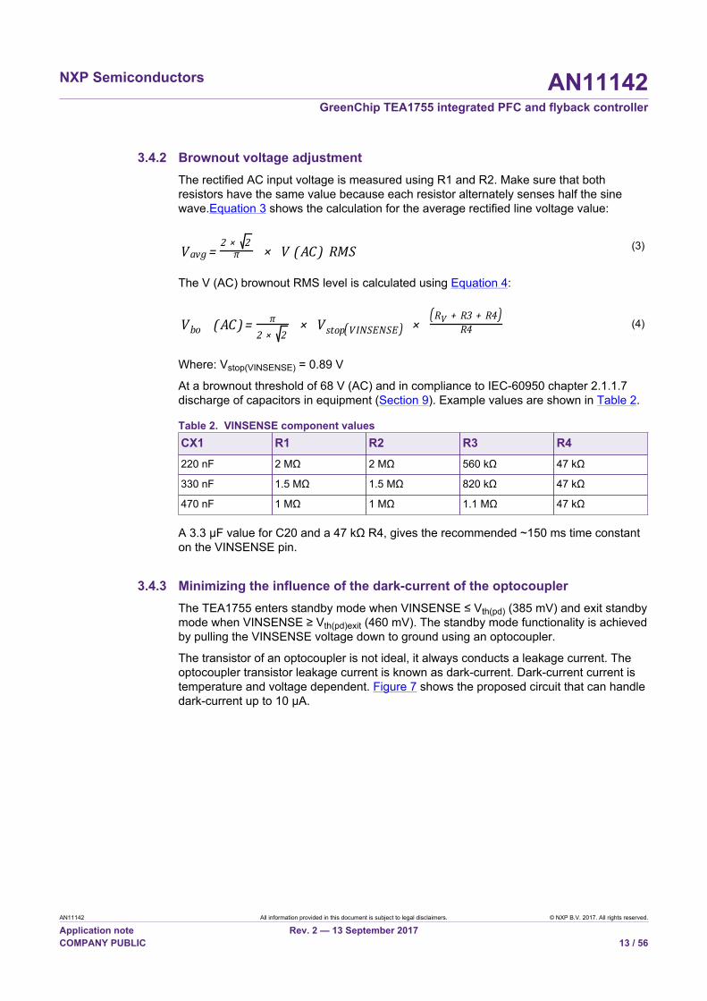
3.4.2 Brownout voltage adjustmentThe rectified AC input voltage is measured using R1 and R2. Make sure that bothresistors have the same value because each resistor alternately senses half the sinewave.Equation 3 shows the calculation for the average rectified line voltage value:
(3)
The V (AC) brownout RMS level is calculated using Equation 4:
(4)
Where: Vstop(VINSENSE) = 0.89 V
At a brownout threshold of 68 V (AC) and in compliance to IEC-60950 chapter 2.1.1.7discharge of capacitors in equipment (Section 9). Example values are shown in Table 2.
Table 2. VINSENSE component valuesCX1 R1 R2 R3 R4220 nF 2 MΩ 2 MΩ 560 kΩ 47 kΩ
330 nF 1.5 MΩ 1.5 MΩ 820 kΩ 47 kΩ
470 nF 1 MΩ 1 MΩ 1.1 MΩ 47 kΩ
A 3.3 μF value for C20 and a 47 kΩ R4, gives the recommended ~150 ms time constanton the VINSENSE pin.
3.4.3 Minimizing the influence of the dark-current of the optocouplerThe TEA1755 enters standby mode when VINSENSE ≤ Vth(pd) (385 mV) and exit standbymode when VINSENSE ≥ Vth(pd)exit (460 mV). The standby mode functionality is achievedby pulling the VINSENSE voltage down to ground using an optocoupler.
The transistor of an optocoupler is not ideal, it always conducts a leakage current. Theoptocoupler transistor leakage current is known as dark-current. Dark-current current istemperature and voltage dependent. Figure 7 shows the proposed circuit that can handledark-current up to 10 μA.

NXP Semiconductors AN11142GreenChip TEA1755 integrated PFC and flyback controller
AN11142 All information provided in this document is subject to legal disclaimers. © NXP B.V. 2017. All rights reserved.
Application note Rev. 2 — 13 September 2017COMPANY PUBLIC 14 / 56
C20 C21
C13
R8
D1000
D1001BD1001A
U2A-1LTV-817B
4
3
R1000R1001
(optional)
R4
R3R2
R1
gate Q8 and Q9
VCC (pin 1)line
neutral
VINSENSE (pin 7)
R45
Q11BC547
019aab513
Figure 7. Proposed VSENSE circuit for minimizing the influence of the dark current
The VINSENSE voltage must reach the Vth(pd)exit before the internal HV current source isenabled. The VCC supply voltage increases and supports any dark-current needed for theoptocoupler. The optocoupler dark-current no longer influences the VINSENSE voltage.
Add the red colored components to the schematic shown in Figure 1. Diode D1001Aand D1001B are available in one component. Remove two resistors (R42 and R43) inFigure 1 when Figure 7 is added.
3.5 Internal OverTemperature Protection (OTP)The IC has an internal temperature protection to protect the IC from overheating. Whenthe junction temperature exceeds the thermal shutdown temperature, the IC stopsswitching. As long as the OTP is active, the VCC capacitor is not recharged from the HVmains. If the VCC supply voltage is not sufficient, the OTP circuit is supplied from the HVpin. OTP is a latched protection.
3.6 LATCH pinThe LATCH pin is a general-purpose input pin which can be used to latch off bothconverters. The pin sources a bias current IO(LATCH) of 30.5 μA for the direct connectionof an NTC. When the voltage on the LATCH pin is pulled below Vprot(LATCH), switching ofboth converters is stopped immediately. VCC starts cycling between the Vth(UVLO) (13.4 V)and Vstartup (22.3 V) without a restart. Switching off the mains input voltage and thenswitching it on triggers the fast-latch reset circuit and resets the latch (see Section 3.7).
At start-up, the LATCH pin is charged above Ven(LATCH) (582 mV) before both convertersare enabled. Charging of the LATCH pin starts when VCC = Vstartup.
A 10 nF capacitor is placed between the LATCH pin and the IC GND pin to prevent falsetriggering. In addition, when the LATCH pin function is not used add a 10 nF capacitor.

NXP Semiconductors AN11142GreenChip TEA1755 integrated PFC and flyback controller
AN11142 All information provided in this document is subject to legal disclaimers. © NXP B.V. 2017. All rights reserved.
Application note Rev. 2 — 13 September 2017COMPANY PUBLIC 15 / 56
ICLATCH
C19
RT2
R26
aaa-002536
5
2GND
Figure 8. Usage of the LATCH pin protection
Latching on application overtemperature occurs when the total resistance value of theNTC plus the series resistor drops under the following:
(5)
3.7 Fast-latch resetSwitching off the mains input voltage and then switching on resets the latchedprotection. After the mains input is switched off, the voltage on the VINSENSE pin drops≤ Vflr (0.75 V). The voltage drop triggers the fast-latch reset circuit but does not reset thelatched protection. After the mains input is switched on, the voltage on the VINSENSEpin rises again. The latch is reset when the level has passed Vflr + Vflr(hys) (0.86 V). Thesystem restarts when the VCC pin is charged to Vstartup (See step 4 of Section 3.2).

NXP Semiconductors AN11142GreenChip TEA1755 integrated PFC and flyback controller
AN11142 All information provided in this document is subject to legal disclaimers. © NXP B.V. 2017. All rights reserved.
Application note Rev. 2 — 13 September 2017COMPANY PUBLIC 16 / 56
4 PFC description and calculation
The PFC controller operates in either QR mode or DCM mode with valley detection toreduce the switch-on losses. The maximum switching frequency of the PFC is limited tofsw(PFC)max (139 kHz) to reduce switching losses. If necessary, one or more valleys areskipped to keep the frequency below 139 kHz.
The PFC is designed as a dual-boost converter with two output voltage levels that aredependent on the mains input voltage range. The advantage is that the overall systemefficiency at low mains is improved because of the reduction of the PFC switching losses.In low and medium power adapters (< 120 W), the contribution of PFC switching lossesto the total losses is relatively high.
An internal current source of 8.1 μA (Ibst(dual)) on the VOSENSE pin controls the dual-output voltage. The mains input voltage measured at the VINSENSE pin is usedto control the internal current source as shown in Figure 9. This current source, incombination with the resistors connected to the VOSENSE pin, sets the lower PFCoutput voltage. At high mains, the current source is switched off. The maximum PFCoutput voltage is unaffected by the current source accuracy. In a typical adapter, witha 385 V (DC) PFC output voltage at high mains, the PFC output voltage is 250 V (DC)at low mains. A voltage of 2.3 V at the VINSENSE pin corresponds with a mains inputvoltage of approximately 170 V (AC). The small slope at the transfer function ensures astable switchover of the PFC output voltage without hiccups.
aaa-004486
2.08 V 2.28 VVVINSENSE
II(VOSENSE)
Figure 9. Transfer function of the VINSENSE voltage to the dual-boost current at VOSENSE
The PFC is switched off to ensure high efficiency during low output currents. After switchoff, the electrolytic bulk capacitor voltage VCbulk drops to line voltage × √2.
4.1 PFC output power and voltage controlThe PFC of the TEA1755 is on-time controlled. So it is not necessary to measure themains phase angle. The on-time is kept constant during the half sine wave to obtain agood Power Factor (PF) and a class-D Mains Harmonics Reduction (MHR).
The PFC output voltage is controlled using the VOSENSE pin. At the VOSENSEpin, there is a transconductance error amplifier with a reference voltage of2.5 V (Vreg(VOSENSE)). The error on the VOSENSE pin is converted with 77 μA/V (gm) to acurrent on the PFCCOMP pin. The voltage on the PFCCOMP pin, in combination with thevoltage on pin VINSENSE, determines the PFC on-time.
NXP Semiconductors AN11142GreenChip TEA1755 integrated PFC and flyback controller
AN11142 All information provided in this document is subject to legal disclaimers. © NXP B.V. 2017. All rights reserved.
Application note Rev. 2 — 13 September 2017COMPANY PUBLIC 17 / 56
VVINSENSE 7
IC
11
6 8
12
VVOSENSE
V/ITRANSDUCER I2
+-
+-
VM
Idch
IchV-
V+
VR
VS
RQ
SVPFCDRIVER
PFCOSCILLATOR
Vosc
VALLEYDETECTION
VPFCAUX
voltage comparator
ramp oscillator
VVALLEY
ton limiting circuit
Icomp
VPFCCOMP
compensation network
C1
C2R1
VREF
transconductanceamplifier
currentmultiplier
I1
I2 Vp
C S
019aab492
Figure 10. TEA1755 PFC converter on-time control
A network with one resistor and two capacitors at the PFCCOMP pin is used to stabilizethe PFC control loop. The equation for a boost converter transfer function contains thesquare of the mains input voltage. In a typical application, the result is a low regulationbandwidth for low mains input voltages and a high regulation bandwidth for high inputvoltages. The result can be that at high mains input voltages, it can be difficult to meetthe MHR requirements. The TEA1755 uses the mains input voltage measured throughthe VINSENSE pin to compensate the control loop gain as a function of the mains inputvoltage. As a result the gain is constant over the entire mains input voltage range.
The voltage on the VINSENSE pin must be an average DC value, representing the mainsinput voltage. The system works optimally with a time constant of approximately 150 mson the VINSENSE pin.

NXP Semiconductors AN11142GreenChip TEA1755 integrated PFC and flyback controller
AN11142 All information provided in this document is subject to legal disclaimers. © NXP B.V. 2017. All rights reserved.
Application note Rev. 2 — 13 September 2017COMPANY PUBLIC 18 / 56
4.1.1 Setting the PFC output voltageThe PFC output voltage is set using a resistor divider between the PFC output voltageand the VOSENSE pin. In normal mode, the PFC output voltage is regulated so that thevoltage on the VOSENSE pin is equal to Vreg(VOSENSE) (2.5 V).
VINSENSE2.1 V
8.1 µA
VVOSENSE
GND
9
2IC
C4
PFC stageD1
C3
VO(PFC)
R6
R6A
R7
place C4 and R7as close aspossible to the IC
aaa-005246
Figure 11. TEA1755 PFC converter output voltage setting
The VOSENSE pin has an integrated protection circuit to detect an open circuitpin (see Section 4.3.2). The open-circuit pin protection operates reliably whenR7 ≤ Vth(stop)VOSENSE(min) / Ibst(dual)max = 0.95 V / 9.1 μA = 104.4 kΩ. The first possibleresistor value (below the 104.4 kΩ) available in the E96 series is 102 kΩ.
Note: MAX is the maximum limiting current value. In data sheet, it is a negative number.Normally, we calculate using positive numbers, so it is called in this application note themaximum value.
Selecting a larger value for R7 can override PFC open-loop protection. The maximumbulk electrolytic capacitor voltage (Vbulk(PFC)high) can be calculated using Equation 6:
(6)
The PFC converter only operates correctly when Vbulk(max) > Vmains(max) × √2 + 10 V(voltage margin). In a universal mains adapter, the highest line voltage is typically 264 V.
Therefore, Vbulk(max) = 264 × √2 + 0 ≈ 383 V. Using this information together withEquation 6 the minimum resistor divider value is calculated (see Equation 7):
(7)
Rewriting Equation 7 results in:
(8)
Vbulk(PFC)low is calculated using:
(9)

NXP Semiconductors AN11142GreenChip TEA1755 integrated PFC and flyback controller
AN11142 All information provided in this document is subject to legal disclaimers. © NXP B.V. 2017. All rights reserved.
Application note Rev. 2 — 13 September 2017COMPANY PUBLIC 19 / 56
At low line voltages, the recommended value for Vbulk(PFC)low ≥ 250 V.
Equation 9 looks as follows when rewritten with the values:
(10)
With R6 + R6A equal to:
(11)
If R6 = R6A, then R6 = 15539 / 2 = 7769 kΩ = 7.77 MΩ.
The calculated Vbulk(PFC)low value fits with the recommended minimum value of 250 Vat low line voltages. Lowering the R7 value results in an increased Vbulk(PFC)low andVbulk(PFC)high. Table 3 shows some calculation examples using R6 = 7680 kΩ andR6A = 7870 kΩ (R6 + R6A = 15550 kΩ).
Table 3. Resistors R6 and R6A calculated using different values for resistor R7R7 (kΩ) R6 + R6A / R7 (kΩ) Vbulk(PFC)low (V) Vbulk(PFC)high (V)102 152.45 258 386
100 155.55 265 394
97.6 159.32 275 403
Note: The selected values for resistor R7 in Table 3 are standard values of the E96series.
When R7 ≤ 104.4 kΩ and Vbulk(PFC)low ≥ 250 V meet their requirements, the results arewithin limits.
Capacitor C4 (see Figure 1) filters noise and prevents protection modes false triggeringbecause of MOSFET switching noise. False triggering of the Vovp(VOSENSE) protection cancause audible noise and disturbance of the AC mains input current.
A time constant between 500 ns and 1 μs at the VOSENSE pin is sufficient, resulting in a4.7 nF C4 capacitor value.
Place R7 and C4 as close as possible to the IC between the VOSENSE pin and the GNDpin.

NXP Semiconductors AN11142GreenChip TEA1755 integrated PFC and flyback controller
AN11142 All information provided in this document is subject to legal disclaimers. © NXP B.V. 2017. All rights reserved.
Application note Rev. 2 — 13 September 2017COMPANY PUBLIC 20 / 56
4.1.2 Calculation of the PFC soft-start and soft-stop componentsSoft-start and soft-stop are implemented using the RC network connected to thePFCSENSE pin.
To enable PFC driver start-up, resistor RSS1 must be ≥ 15 kΩ minimum value to ensurethat the Vstart(soft)PFC voltage of 0.5 V is reached. See Section 3.2 for a description ofstart-up.
SOFT-STARTSOFT-STOPCONTROL
OCP11PFCSENSE
0.5 V
Istart(soft)PFC ≤ 60 AQ1
RSS1
CSS1Rsense
019aab493
IC
Figure 12. PFC soft start and soft stop
The total soft-start or soft-stop time is tsoft-start = 3 × RSSI × CSSI.
Switching off the PFC always ends with a soft stop. However, there is an exception tothis rule. The switched on PFC does not generate a soft stop when the system entersburst mode even though CSS1 charges up to Vsense(PFC)max after switching off the PFC.The charged CSS1 capacitor allows a fast restart of the PFC when applicable.
Keep the soft-start time of the PFC shorter than the soft-start time of the flybackcontroller. It is also recommended that the soft-start time is kept within a range of 2 ms to5 ms.
Using C6 = 100 nF and R11 = 15 kΩ results in a soft-start time of 4.5 ms.
4.2 PFC demagnetizing and valley detectionThe PFC MOSFET is switched on after the transformer is demagnetized. The internalcircuitry connected to the PFCAUX pin detects the end of the secondary stroke. It alsodetects the voltage across the PFC MOSFET. The next primary stroke is started whenthe voltage across the PFC MOSFET is at its minimum level. When the voltage is atthe minimum level, switching losses and ElectroMagnetic Interference (EMI) (valleyswitching) are reduced.
To reduce the switching losses, the PFC converter maximum switching frequency islimited to 139 kHz. If necessary, one or more valleys are skipped to keep the frequencyunder 139 kHz.
When demagnetization is not detected on the PFCAUX pin, the controller generatesa Zero-Current Signal (ZCS) 48 μs (tto(demag)PFC) after the last PFC gate signal. Ifa valley signal is not detected on this pin, the controller generates a valley signal4.2 μs (tto(demag)PFC) after demagnetization was detected.

NXP Semiconductors AN11142GreenChip TEA1755 integrated PFC and flyback controller
AN11142 All information provided in this document is subject to legal disclaimers. © NXP B.V. 2017. All rights reserved.
Application note Rev. 2 — 13 September 2017COMPANY PUBLIC 21 / 56
019aab478
C1 C2
L1L29
5
7
1
R27
R9
Q1
D1
C3
PFCAUX
GND
PFCDRIVER12
8
2
IC
Figure 13. TEA1755 PFCAUX circuitry
4.2.1 Design of the PFCAUX winding and circuitSet the voltage on pin PFCAUX as high as possible within the absolute maximum voltagerating of ±25 V. This setting guarantees valley detection at low ringing amplitudes.
The number of turns of the PFCAUX winding is calculated using Equation 12.
(12)
Where:
• VPFCAUX is the absolute maximum rating of the PFCAUX pin• VL(max) is the maximum voltage across the PFC primary winding
The PFC output voltage at the PFC OVP level determines the maximum voltage acrossthe PFC primary winding and is calculated using Equation 13:
(13)
When a PFC coil with a higher number of auxiliary turns is used, place a resistor voltagedivider between the auxiliary winding and the PFCAUX pin. The total resistive valueof the divider must be ≤ 10 kΩ to prevent a valley detection delay due to parasiticcapacitance.
The polarity of the signal at the PFCAUX pin is reversed compared to the PFC MOSFETdrain signal.
To protect against electrical overstress during lightning surge events, add a 5 kΩ resistorbetween the PFC auxiliary winding and the PFCAUX pin. To prevent incorrect valleyswitching of the PFC because of external disturbances, place the resistor as close aspossible to the IC.

NXP Semiconductors AN11142GreenChip TEA1755 integrated PFC and flyback controller
AN11142 All information provided in this document is subject to legal disclaimers. © NXP B.V. 2017. All rights reserved.
Application note Rev. 2 — 13 September 2017COMPANY PUBLIC 22 / 56
4.3 PFC protection modes
4.3.1 VOSENSE overvoltage protectionOvervoltage can occur across the bulk electrolytic capacitor during the initial start-upand large load changes. The relative slow response of the PFC control loop causes thisovervoltage. The PFC control loop response must be relatively slow to guarantee a goodpower factor and meet the MHR requirements. The OverVoltage Protection (OVP) on theVOSENSE pin limits the overvoltage.
When the Vovp(VOSENSE) level = 2.62 V is detected, the PFC MOSFET is switched offimmediately regardless of the on-time setting. The switching of the MOSFET is blockeduntil the voltage on the VOSENSE pin drops < 2.62 V again. OVP is also triggered whenthe resistor between the VOSENSE pin and ground is open. The peak voltage during anovershoot across the electrolytic bulk capacitor is calculated using Equation 14.
(14)
4.3.2 VOSENSE open and short pin detectionThe VOSENSE pin senses the PFC output voltage. The VOSENSE pin has an integratedprotection circuit to detect an open and short circuited pin. The VOSENSE pin alsosenses that one of the resistors in the voltage divider is open making the VOSENSE pinfail-safe.
It is not necessary to add an external OVP circuit for the PFC.
When the pin is open, an internal current source pulls VVOSENSE up and VOVP(VOSENSE)is detected. The PFC stops switching when VOVP(VOSENSE) is detected and an internalvoltage clamp limits the maximum VOSENSE voltage. The same condition applies whenonly resistor R7 is open (see Figure 11). The internal voltage clamp again limits themaximum VOSENSE voltage to acceptable values.
The PFC is not switching when VVOSENSE ≤ VVth(stop)VOSENSE, this condition is applicablewhen VOSENSE is short circuited to ground. The same condition is applicable ifonly resistor R6 or R6A (see Figure 11) is open. However under the condition thatR7 ≤ 104.4 kΩ (see Section 4.1.1).
4.3.3 VINSENSE open pin detectionThe VINSENSE pin senses the mains input voltage, The VINSENSE pin has aprotection circuit to detect an open pin. An internal current source pulls down the pin to≤ Vstop(VINSENSE) (0.89 V) when the pin is open.
NXP Semiconductors AN11142GreenChip TEA1755 integrated PFC and flyback controller
AN11142 All information provided in this document is subject to legal disclaimers. © NXP B.V. 2017. All rights reserved.
Application note Rev. 2 — 13 September 2017COMPANY PUBLIC 23 / 56
4.3.4 Overcurrent protectionThe overcurrent protection limits the maximum current through the PFC MOSFETand PFC coil. The current is measured via a current sense resistor in series with theMOSFET source. The MOSFET is switched off immediately when the voltage on thePFCSENSE pin exceeds the Vsense(PFC)max level of 495 mV at dV/dt = 0 mV/μs. OCP is acycle-by-cycle protection.
To avoid false triggering of the PFC OCP by the flyback converter switching, use a100 mV margin. False triggering of the Vsense(PFC)max protection can cause interferenceto the AC mains input current. To suppress any external disturbance, place a smallcapacitor between 100 pF and 220 pF next to the PFCSENSE pin.
The current sense resistor is calculated using Equation 15:
(15)
Where: the maximum PFC peak current is IpQR(PFC)max at the high output load and lowmains.
The maximum peak current for the PFC operating in Quasi-Resonant (QR) mode iscalculated using Equation 16:
(16)
Where:
• Po(max) is the maximum output power of the flyback• Factor 1.1 is used to compensate the dead-time between zero-current in the PFC
inductor at the end of the secondary stroke and the detection of the first valley in quasi-resonant mode
• η is the expected efficiency of the total converter at maximum output power• V(AC)min is minimum mains input voltage.

NXP Semiconductors AN11142GreenChip TEA1755 integrated PFC and flyback controller
AN11142 All information provided in this document is subject to legal disclaimers. © NXP B.V. 2017. All rights reserved.
Application note Rev. 2 — 13 September 2017COMPANY PUBLIC 24 / 56
5 Flyback description and calculation
5.1 Flyback output power controlThe TEA1755 flyback system waits until the transformer is demagnetized and at leastone valley has appeared before it is magnetized again for the next cycle. The FBAUX pindetects demagnetization via the auxiliary winding. The HV pin detects the bottom of thevalley via the drain of the MOSFET or the central tap of the primary winding.
The output power (PO) of the flyback is calculated using Equation 17:
(17)
Where:
• Lp is the flyback transformer primary inductance• Ipk is the flyback transformer primary peak current• fs is the flyback controller operating frequency• η is the flyback controller efficiency
Lp is selected at the start of the design. The primary peak current controls the (high)output power in QR and DCM mode. The switching frequency is a result of externalapplication parameters and IC parameters.
External application parameters are the transformer turns ratio, primary inductance, thedrain source capacitance, input voltage, output voltage, and the feedback signal from thecontrol loop. IC parameters are the oscillator setting, the peak current setting, and thedemagnetization and valley detection.
The primary current Ipk is fixed at medium and low output power. The power is controlledby changing the operating frequency. Output power and operating frequency arelinearly related during this type of control. In this application note, it is called operatingin frequency reduction mode (See Section 5.1.1.3). The minimum switching frequencyin FR mode is 25 kHz. At even lower output powers, the IC enters the burst mode whichminimizes audible noise.
The burst mode is a hysteresis controlled system, used during low output-power. Theprimary peak current Ipk and operating frequency of the flyback are both fixed when thesystem supports power to the output.
Using VFBCTRL as a hysteresis input results in a variable number of FBDRIVER switchingpulses combined with a changing burst mode repetition frequency.
The flyback input voltage is measured using the FBAUX pin and it is used to implementan OverPower Protection (OPP). OPP keeps the maximum output power of the flybackconverter constant over the input voltage.
The flyback has an accurate OverVoltage Protection (OVP) circuit. The overvoltage ismeasured through the FBAUX pin. Both flyback and PFC controllers are switched off in alatched protection when an overvoltage is detected.

NXP Semiconductors AN11142GreenChip TEA1755 integrated PFC and flyback controller
AN11142 All information provided in this document is subject to legal disclaimers. © NXP B.V. 2017. All rights reserved.
Application note Rev. 2 — 13 September 2017COMPANY PUBLIC 25 / 56
5.1.1 Four TEA1755 operation modesAt initial start-up, the flyback always starts at the maximum output power. So, the systemstarts up in Quasi-resonant mode. The flyback of the TEA1755 passes through fouroperation modes (see Figure 14) from maximum to minimum output power:
• Quasi-Resonant (QR) mode• Discontinuous Conduction Mode (DCM)• Frequency Reduction (FR) mode• Burst Mode (BM)
The internal demagnetization detection and valley switching circuitry is active in all fouroperating modes.
aaa-002672
VFBCTRL (V)
PFC off PFC on
flybackswitching
frequency
fsw(fb)max
4.94.02.82.40.77
burst modefrequency
FR minimumfrequency
FR DCM QR
BM
QR: Quasi ResonantDCM: Discontinuous Conduction Mode
FR: Frequency ReductionBM: Burst Mode
Figure 14. Flyback operation modes
5.1.1.1 Quasi-resonant mode
The flyback operates in quasi-resonant mode at high and maximum output power. Thepeak current controls the output power (see Section 5.1). A lower peak current than themaximum allowed value results in lower output power and a higher operating frequencyuntil the maximum operating frequency is reached. The quasi-resonant mode can easilybe recognized. The next primary switching cycle starts when the bottom of the first valleyis detected.
The voltage on the FBCTRL pin sets the primary peak current (Ipk). To avoid flybackcontroller interference by the PFC MOSFET switching, place the 220 pF noise filtercapacitor (C15) as close as possible to the FBCTRL pin. The voltage on the FBCTRL pinis measured back at the FBSENSE pin and is calculated using Equation 18 (only valid inQR mode or DCM):
(18)

NXP Semiconductors AN11142GreenChip TEA1755 integrated PFC and flyback controller
AN11142 All information provided in this document is subject to legal disclaimers. © NXP B.V. 2017. All rights reserved.
Application note Rev. 2 — 13 September 2017COMPANY PUBLIC 26 / 56
Where:
• VFBCTRL is allowed to vary between the 4 V and 4.9 V (only valid in QR mode and DCMmode)
• Iadj(FBSENSE) related to a current source inside the IC, connected to the FBSENSE pin• Resistors R16 and R17 are found in the circuit diagram, see Figure 15.
C10
FBSENSER16
Lp
Q2
Rsense
Rcomp
C23
R16A
FBDRIVERRSERIES = R17 + R16
Vi (DC)
R17
T1
Coutput
Doutput
019aaa039
Iadj(FBSENSE)
The FBSENSE pin has two internal reference levels:(1) Vsense(fb)max = 545 mV at dV/dt = 0 mV/μs(2) Vsense(fb)min = 232 mV at dV/dt = 0 mV/μs
Figure 15. Most important components for adjusting the flyback in the application
Equation 19 defines the peak current Ipk through the flyback transformer:
(19)
Vsense(fb)max determines the maximum peak current Ipk(max). Resistor R16A is notmentioned in Equation 18 and Equation 19. However, resistor R16A is explained inSection 5.1.5. Decreasing the output power results in the flyback entering discontinuousconduction mode when the maximum switching frequency is reached.
5.1.1.2 Discontinuous conduction mode
Reducing the peak current (Ipk) and skipping more valleys decreases the output power. Itresults in a switching frequency close to but never higher than fsw(PFC)max (139 kHz). Theoperating mode switches from DCM to FR mode when VFBCTRL = 4 V (Vstart(red)f)).
Sometimes DCM is not reached when the selected primary inductance of the inductoris too large. In this case, flyback skips DCM when it is reducing power. It jumps directlyfrom QR mode to FR mode.
5.1.1.3 Frequency reduction mode and PFC switch on/switch off control
The voltage across the FBCTRL pin in Frequency reduction mode does not set the peakcurrent, instead it sets the operating frequency. The minimum primary peak currentIpk(min) through the flyback transformer is kept constant during FR mode.
The ratio Ipk(min) : Ipk(max) mainly depends on the sense resistor Rsense value assumingthat the core is not saturated at Ipk(max). Decreasing the output power reduces theoperating frequency. As a result of the frequency reduction, more valleys are skipped.

NXP Semiconductors AN11142GreenChip TEA1755 integrated PFC and flyback controller
AN11142 All information provided in this document is subject to legal disclaimers. © NXP B.V. 2017. All rights reserved.
Application note Rev. 2 — 13 September 2017COMPANY PUBLIC 27 / 56
The flyback operating frequency during FR mode determines when the PFC is switchedon or switched off.
Decreasing the output-power from maximum to minimum switches off the PFC beforeit has reached 25 % of the nominal output current. Switching off the PFC improves theoverall efficiency at low output power.
Increasing the output-power from minimum to maximum starts the PFC up before it hasreached 50 % of the nominal output current. Starting up the PFC improves the powerfactor of the line current at high output power.
The PFC switch-on/switch-off state depends on the primary inductance value, the outputpower, and the line voltage. It is therefore, important to select the right inductance valueto ensure enough hysteresis between the PFC switch-on/switch off state, especially atlow line voltages (see Section 5.1.2).
The following three options are used to switch on the PFC:
1. The PFC is using the flyback operating frequency during FR mode (f ≥ fsw(fb)swon(PFC)).2. VFBCTRL ≥ Ven(PFC)FBCTRL (3.75 V), applicable at initial start-up or when the flyback
operating frequency cannot reach fsw(fb)swon(PFC).3. When the duty cycle of the FBDRIVER ≥ 50 %.
Option 3 is useful during line dips, assuming that some residual line voltage is presentthat can support power. The flyback can support more power to the output when its inputvoltage is higher (because of the switched on PFC). So, it can hold the nominal outputvoltage for a longer time.
Table 4. PFC switch-on and switch-off signalsThe table does not list the PFC table override function. See Section 5.2.1 and Section 5.2.2.
Options PFC switch-on signal PFC switch-off signal1 fsw(fb) ≥ 73 kHz fsw(fb) ≤ 53 kHz
2 VFBCTRL ≥ 3.75 V -
3 δFBDRIVER ≥ 50 %
Note: VINSENSE ≤ Vstop(VINSENSE) switches off the PFC, regardless which PFC switch-on signal is used.
The minimum operating frequency during FR mode is 25 kHz. This frequency is abovethe audible frequency for humans.
5.1.1.4 Burst mode
Requesting less output power activates the frequency clamp and the flyback controllerstarts to operate in burst mode. The PFC continues to operate if it was switching. ThePFC stops switching when VPFCTIMER ≥ Vstop(PFCTIMER) (3 V). The internal circuitry of theTEA1755 is partly shut down, resulting in a reduced supply current.
The peak current Ipk(min) during burst mode is equal to the value in FR mode.
The burst mode repetition frequency and number of FBDRIVER pulses depends on thefeedback loop and output power.
The maximum burst mode repetition frequency is preferably below the 700 Hz, someadjustment can be made by changing the value of R34. A relatively low burst moderepetition frequency minimizes the risk on audible noise.
NXP Semiconductors AN11142GreenChip TEA1755 integrated PFC and flyback controller
AN11142 All information provided in this document is subject to legal disclaimers. © NXP B.V. 2017. All rights reserved.
Application note Rev. 2 — 13 September 2017COMPANY PUBLIC 28 / 56
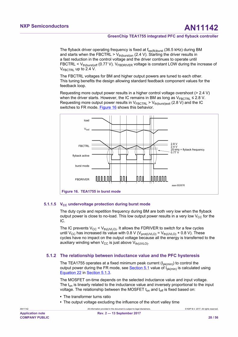
The flyback driver operating frequency is fixed at fsw(fb)burst (36.5 kHz) during BMand starts when the FBCTRL > Vth(burst)on (2.4 V). Starting the driver results ina fast reduction in the control voltage and the driver continues to operate untilFBCTRL < Vth(burst)off (0.77 V). VFBDRIVER voltage is constant LOW during the increase ofVFBCTRL up to 2.4 V.
The FBCTRL voltages for BM and higher output powers are tuned to each other.This tuning benefits the design allowing standard feedback component values for thefeedback loop.
Requesting more output power results in a higher control voltage overshoot (> 2.4 V)when the driver starts. However, the IC remains in BM as long as VFBCTRL ≤ 2.8 V.Requesting more output power results in VFBCTRL > Vth(burst)exit (2.8 V) and the ICswitches to FR mode. Figure 16 shows this behavior.
aaa-002676
load
Vout
FBCTRL
flyback active
burst mode
FBDRIVER
2.8 V2.4 V25 kHz = flyback frequency0.77 V
Figure 16. TEA1755 in burst mode
5.1.1.5 VCC undervoltage protection during burst mode
The duty cycle and repetition frequency during BM are both very low when the flybackoutput power is close to no-load. This low output power results in a very low VCC for theIC.
The IC prevents VCC < Vth(UVLO). It allows the FDRIVER to switch for a few cyclesuntil VCC has increased its value with 0.8 V (Vprot(UVLO) = Vth(UVLO) + 0.8 V). Thesecycles have no impact on the output voltage because all the energy is transferred to theauxiliary winding when VCC is just above Vth(UVLO).
5.1.2 The relationship between inductance value and the PFC hysteresisThe TEA1755 operates at a fixed minimum peak current (Ipk(min)) to control theoutput power during the FR mode, see Section 5.1 value of Ipk(min) is calculated usingEquation 22 in Section 5.1.3.
The MOSFET on-time depends on the selected inductance value and input voltage.The ton is linearly related to the inductance value and inversely proportional to the inputvoltage. The relationship between the MOSFET ton and toff is fixed based on:
• The transformer turns ratio• The output voltage excluding the influence of the short valley time

NXP Semiconductors AN11142GreenChip TEA1755 integrated PFC and flyback controller
AN11142 All information provided in this document is subject to legal disclaimers. © NXP B.V. 2017. All rights reserved.
Application note Rev. 2 — 13 September 2017COMPANY PUBLIC 29 / 56
The relatively large inductance results in the flyback running in QR mode at low linevoltages although the flyback controller is running in FR mode. This situation is easy torecognize. FBDRIVER is immediately activated at the bottom of the first valley. (Normaloperation usually skips valleys during FR mode). Figure 17 shows the operation of aflyback controller at low and lower line voltages.
tp ts
Is
Is
tp
T = 1 / fs
ts
ts
tx
T + tx = 1 / fs-low
ts
tvalley
(1)
(2)
Ipk(min) = fixed value
Ipk(min) = fixed value
tvalley
tp + txtp + tx
aaa-005247
(1) Flyback controller driven at low line voltages assuming a relatively large primary inductance for the flybacktransformer.(2) Flyback controller driven at very low line voltages assuming a relatively large primary inductance for the flybacktransformer.
Figure 17. Operating frequency as a function of low line voltages, assuming a relatively high selected primaryinductance value for the flyback transformer
Lowering the line voltage results in a lower operating frequency and output power whenthe selected primary inductance is relatively high.
In practice, the flyback driver supports a limited amount of power at low line voltages.Requesting more power activates the feedback loop and the PFC controller starts up at alower output power than was originally intended. The hysteresis between PFC switch-onand switch-off becomes smaller therefore at low line voltages. The PFC starts switchingwhen VFBCTRL ≥ Ven(PFC)FBCTRL = 3.75 V, if the flyback operating frequency cannot reachfsw(fb)swon.
Normally, a relatively high primary inductance value is preferred because it minimizesswitching losses. However, it must not result in unwanted system behavior at low line

NXP Semiconductors AN11142GreenChip TEA1755 integrated PFC and flyback controller
AN11142 All information provided in this document is subject to legal disclaimers. © NXP B.V. 2017. All rights reserved.
Application note Rev. 2 — 13 September 2017COMPANY PUBLIC 30 / 56
voltages because of lost hysteresis. Limiting the maximum inductance value preventsany unwanted system behavior at low line voltages. In addition, a longer valley timemakes the hysteresis between PFC switch-on and switch-off even smaller. Keep thevalley time close to 1.1 μs.
It is helpful to have an indication of the acceptable maximum transformer primaryinductance value at the start of the design. Several assumptions are made whencalculating these inductance values as shown in Figure 18. Therefore, these values areonly for use as indications.
(1)
(2)
(3)
(4)
019aaa041
PO (W)75 15513511595
400
600
800
Lp(µH)
200
(5)
Lp = f(PO)Assumptions: Minimum voltage across the buffer capacitor (C3) is approximately 100 V (DC)at 50 % of the nominal output power.(1) N × (VO + Vf) = 80 V(2) N × (VO + Vf) = 92 V(3) N × (VO + Vf) = 104 V(4) N × (VO + Vf) = 118 V(5) N × (VO + Vf) = 130 V
Figure 18. Indication of the maximum primary inductance value, related to output powerand N × (VO + Vf)
Figure 18 shows an indication for the maximum primary flyback inductance value atdifferent output powers and turn ratios.
The following effects are seen for the primary inductance:
• Selecting a higher value results in a reduction of the PFC switch on and switch offhysteresis
• Selecting a lower value results in lower efficiency (related to more overall switchinglosses)
The inductance values shown in Figure 18 result in the loss of some hysteresis at≤ 115 V (AC) line voltage. However, the hysteresis is still acceptable at 90 V (AC),assuming that the voltage across C3 does not drop under approximately 100 V (DC) at50 % of the nominal load.
Usually this minimum voltage condition is achieved when C3 in μF is equal to the nominaloutput power in W as a rule of thumb. The assumption is the minimum line voltage is90 V (RMS)/60 Hz and PPFC(swon) ≤ 0.5 × Pnominal
NXP Semiconductors AN11142GreenChip TEA1755 integrated PFC and flyback controller
AN11142 All information provided in this document is subject to legal disclaimers. © NXP B.V. 2017. All rights reserved.
Application note Rev. 2 — 13 September 2017COMPANY PUBLIC 31 / 56
The following methods can be used to select the inductance value:
• using Figure 18• using Equation 20
(20)
Where:
• IO(nom) stands for the nominal output current according to the type plate of the adapter• VO the output voltage• Vf the forward voltage across the secondary diode• Lp the flyback transformer primary inductance• N the turns ratio between the primary and secondary windings (Np/Ns)
Equation 20 gives some deviation at a low and a high value of the N × (VO + Vf) product.Keep this value between 80 V and 130 V.
Example:
• IO(nom) = 4.62 A• VO = 19.5 V• Vf = 0.1 V• N × (VO + Vf) = 104.5
The final value used is 450 μH.
5.1.3 Relationship between Ipk(min) and the required PFC(swon)/PFC(swoff) levelThe PFC is switched on and switched off usually between 50 % and 25 % of the nominaloutput current of the flyback. The PFC is only switched on or switched off when theflyback controller is running in FR mode. The PFC switches on at a flyback operatingfrequency of 73 kHz (fsw(fb)swon(PFC)) and switches off the PFC at 53 kHz (fsw(fb)swoff(PFC)).
The recommended PFC switch off output power is 30.3 % of the typical output-power.The margin between 30.3 % and the 25 % requirement is used for a range of tolerances.Use components with a tolerance values that comply with the components given inthe Bill Of Materials section of the UM10514 user manual (see Section 9). Allowingmore tolerance for the components requires a larger margin for the recommendedoutput power when a 25 % power requirement is met. Using this information results inEquation 21:
NXP Semiconductors AN11142GreenChip TEA1755 integrated PFC and flyback controller
AN11142 All information provided in this document is subject to legal disclaimers. © NXP B.V. 2017. All rights reserved.
Application note Rev. 2 — 13 September 2017COMPANY PUBLIC 32 / 56
(21)
or:
(22)
Where:
• 0.303 is the recommended multiplying factor related to PFC(swoff)• VO is the output voltage• IO(nom) is the nominal output current according to the type of adapter plate• Vf is forward voltage across the secondary diode• Lp is the primary inductances of the flyback transformer• fsw(fb)swoff(PFC) is 53000• ηfb is the efficiency of the flyback (use relatively high values, such as 0.94 to 0.96)
Example:
• IO(nom) = 4.62 A• VO = 19.5 V• Vf = 0.1 V• Lp = 450 μH• ηfb = 0.95
PFC(swon) is calculated using Equation 23:
(23)
Using the data results in:
This value can be translated into an output current Iout(en):
(24)

NXP Semiconductors AN11142GreenChip TEA1755 integrated PFC and flyback controller
AN11142 All information provided in this document is subject to legal disclaimers. © NXP B.V. 2017. All rights reserved.
Application note Rev. 2 — 13 September 2017COMPANY PUBLIC 33 / 56
5.1.4 The influence of Rsense and the R16/R17 series resistanceThe sense resistor, Rsense, together with the series impedance R16 and R17, has fourfunctions:
• prevent or minimize the risk of saturation of the flyback transformer• allow enough power to the output (assuming the inductance is not going into saturation)• allow some adjustment for switching on or switching off the PFC at a certain output
power level. The value of Rsense is more dominant for this adjustment than the value ofR16, as its influence is much smaller
• R17 and C23 prevent FBSENSE being charged negative because of disturbancesacross Rsense
The saturation level (Isat) of the transformer and the value of the sense resistor areimportant design parameters. Section 5.1.4.1 shows the calculation for the transformersaturation level. Next, the maximum peak current (Ipk(max)) through the transformer isdetermined. This value is preferably below the transformer saturation level.
5.1.4.1 Calculating the flyback transformer saturation current Isat
The transformer saturation level is calculated using Equation 25.
(25)
Example based on the following assumptions:
• Np = 32 turns• Bmax = 390 mT (PQ3220, material PC44, Bmax at 100 °C)• Ae = 170 × 10−6 m2 (from transformer supplier data sheet)• Lp = 450 × 10−6
Result:
Values for Ae and Bmax are contained in the transformer data sheet. The Bmax valuedepends on temperature. It decreases rapidly at high operating temperatures. Therefore,select the Bmax value at high operating temperatures. Core saturation does not occurwhen the maximum peak current (Ipk(max)) is less than the saturation current (Isat).Section 5.1.4.2 shows the calculation of Ipk(max). A saturated core deteriorates the overallsystem performance. It results in more stress, EMI and in the worst case, a possiblesystem failure.
NXP Semiconductors AN11142GreenChip TEA1755 integrated PFC and flyback controller
AN11142 All information provided in this document is subject to legal disclaimers. © NXP B.V. 2017. All rights reserved.
Application note Rev. 2 — 13 September 2017COMPANY PUBLIC 34 / 56
5.1.4.2 Calculation of Ipk(max) for flyback operating in Quasi-resonant mode
The flyback peak current in QR mode is calculated using Equation 26:
(26)
Where:
• a = N × Vi(DC)min × Lp• b = −2 × IO × Lp × {N × (VO + Vf) + Vi(DC)min}• c = −2 × IO × tvalley × N × Vi(DC)min × (VO + Vf)
For a, b and c:
• VO is the output voltage• N is the turns ratio between the primary and secondary windings (Np/Ns)• Vf is the forward voltage across the secondary diode• Lp is the inductance value of the primary winding• tvalley is the valley time, sometimes also described as dead-time. This time is usually
around the 1.1 μs• Vi(DC)min is the minimum voltage across electrolytic bulk capacitor C3 during a load-
step. The customer defines the load step but the maximum value of the load stepis limited to the nominal output power. In this example, Vi(DC)min = 75 V (DC). Thevoltage depends on the load step, the value of the Cbulk and when the PFC is switchedon during the mains cycle. It is recommended that this value is checked in everyapplication.
Examples:
• a = 5.3333 × 75 × 450× 10−6 = 180 × 10−3
• b = −2 × 4.62 × 450 × 10−6 × {5.3333 × (19.5 + 0.1) + 75} = −746.499 × 10⁻³
• c = −2 × 4.62 × 1.1 × 10−6 × 5.3333 × 75 × (19.5 + 0.1) = −79.6875 × 10⁻³
(27)
The calculated peak current is under the 4.71 A saturation level (see Section 5.1.4.1).Allow a margin between the calculated value and the saturation level of the core. Forexample, the system could still run into a problem during a peak load. Check carefully forthese instances in the final design.
Assuming the PFC has been switched on for some time, Equation 28 shows the resultsusing a peak output current of 5.7 A and Vbulk = 250 V (DC).
• a1 = 5.3333 × 250 × 450 × 10−6 = 0.6• b1 =−2 × 5.70 × 450 × 10−6 × {5.3333 × (19.5 + 0.1) + 250} = −1.8188• c1 = −2 × 5.70 × 1.1 × 10−6 × 5.3333 × 250 × (19.5 + 0.1) = −32.77 × 10⁻³

NXP Semiconductors AN11142GreenChip TEA1755 integrated PFC and flyback controller
AN11142 All information provided in this document is subject to legal disclaimers. © NXP B.V. 2017. All rights reserved.
Application note Rev. 2 — 13 September 2017COMPANY PUBLIC 35 / 56
(28)
Select the highest Ipk(max) value (with IO = 4.62 A and IO = 5.7 A). Compare the Ipk(max)value with the Isat value. The highest Ipk(max) value must be lower than the Isat value.
If so, use the Isat value for Ipmax to allow a better maximum output power margin.
5.1.4.3 Calculation of the current sense resistor Rsense
The next step is calculating the Rsense value, see Equation 29:
(29)
Note: fill in the highest for Ipk(max) level (see Section 5.1.4.2).
Using the saturation current Isat for Ipk(max) is often preferred (assuming that Isat > Ipk(max))because it allows a higher maximum output power.
Using the highest peak current of all (Isat = 4.715 A, see Section 5.1.2) results in a valuefor Rsense as calculated in Equation 30:
(30)
5.1.4.4 Calculation of the series resistance R16 and R17
Equation 31 calculates the series resistance of R16 and R17:
(31)
A typical 90 W adapter example:
The value of R17 is often roughly between 680 Ω and 1.2 kΩ. Its purpose is to preventC10 being charged in an unwanted way because of spikes across Rsense which cantrigger the internal ESD protection. Selecting a value between these two limits allowssome freedom for trimming R16 or the delay compensation resistor R16A. When the R17value is chosen as 1000 Ω, R16 = 37100 Ω − 1000 Ω = 36100 Ω.

NXP Semiconductors AN11142GreenChip TEA1755 integrated PFC and flyback controller
AN11142 All information provided in this document is subject to legal disclaimers. © NXP B.V. 2017. All rights reserved.
Application note Rev. 2 — 13 September 2017COMPANY PUBLIC 36 / 56
5.1.5 Calculation of the delay compensation resistors Rcomp and R16ARcomp and R16A are intended to compensate the sum of the following three delays:
• the internal delay time of the IC• the switch off time of the MOSFET• the delay time related to R17 × C23 (filter in front of the FBSENSE pin)
The transformer still conducts current on the primary side during the sum of all thesedelay times. These delay times are translated into an extra current IDELAY through thetransformer (see Figure 19) which results in extra output energy. The amount of extraenergy depends on the input voltage.
The current flows through two resistors placed in series, R5 and R5A. The combinedresistance of R5 and R5A resistors is called Rcomp. Select Rcomp ≤ 13.6 MΩ.
Rcomp is calculated using Equation 32:
(32)
Resistors Rcomp and R16A compensate for the unwanted current (IDELAY) using acorresponding delay time.
The voltage across R16A is translated to the current IPRESET with the correspondingpreset time. When the preset values cancel the delay values, the system iscompensated.
The voltage across resistor R16A depends on the current passing through it.
IDELAY
IPREFERRED
tPREFERRED
IPRESET
tDELAYtPRESET
019aaa042
Figure 19. Principle of delay compensation
An example calculation for a typical 90 W adapter: Rcomp = 6.8 + 6.8 = 13.6 MΩ
The IC internal delay time, MOSFET switch off response time and the R17 × C23 timeconstant determine the final delay time. A minimum RC time is required to filter outdisturbances on the FBSENSE pin.
An RC time selection that is too large cannot follow the input voltage ramp-up properly.All other delays are subtracted first from the flyback MOSFET conducting time. Theremaining time must be at least 5.5 times the minimum RC time required for filtering outinterference on the FBSENSE pin.

NXP Semiconductors AN11142GreenChip TEA1755 integrated PFC and flyback controller
AN11142 All information provided in this document is subject to legal disclaimers. © NXP B.V. 2017. All rights reserved.
Application note Rev. 2 — 13 September 2017COMPANY PUBLIC 37 / 56
td(FBDRIVER) defines the internal delay of the TEA1755 at 80 ns. Switching off theMOSFET usually takes around 60 ns.
Note: Check the time for switching off the MOSFET (td(MOSFET)off) in the final applicationbecause using different MOSFETs and gate resistors can change its duration.
The conduction time of the flyback MOSFET is shortest when the input voltage is at itshighest. The highest value is usually 390 V (DC). Equation 33 shows the calculation forR17 × C23:
(33)
An example calculation for a typical 90 W adapter:
A commonly used RC time for this filter is 220 ns using 1 kΩ for resistor R17 and 220 pFfor capacitor C23. The RC time value is used in the subsequent equations. The toleranceof capacitor C23 is ≤ 10 %.
Using a maximum tolerance of 10 % for C23 limits the impact on the overall spreading forthe PFC(swon) on and PFC(swoff) level.
The output follows the input with a delay of just one RC time after roughly five RC times.The total delay time is calculated using Equation 34:
(34)
An example for a typical 90 W adapter:
The R16A value is calculated using Equation 35:
(35)
An example for a typical 90 W adapter:

NXP Semiconductors AN11142GreenChip TEA1755 integrated PFC and flyback controller
AN11142 All information provided in this document is subject to legal disclaimers. © NXP B.V. 2017. All rights reserved.
Application note Rev. 2 — 13 September 2017COMPANY PUBLIC 38 / 56
5.1.6 Calculation of flyback soft start componentsSoft start is implemented using the RC network connected to the FBSENSE pin.
The sum of resistors R16, R16A, and R17 must be > 15 kΩ to ensure Vstart(soft)fb (0.55 V)is reached and flyback start-up is enabled. See the TEA1755T and TEA1755LT datasheets (see Section 9).
In general, the R16A and R17 values are much smaller than the value of R16. Therefore,the soft-start time is: τsoft-start ≈ 3 × R16 × C10.
Make τsoft-start for flyback longer than for the PFC. Keep τsoft-start in the range of 5 ms to10 ms. When C10 = 68 nF and R16 = 36 kΩ, the total tsoft-start is approximately 7 ms.
5.2 Two PFCTIMER pin optionsThe PFCTIMER pin can be used to extend the PFC operating time when the outputpower drops below the PFC switch off level. This option prevents the PFC fromconstantly switching on and off because of fast, large dynamic load changes at theoutput. Preventing that the PFC switches on and off results in reduced audible noise.This option is further described in Section 5.2.1.
Another option for the PFCTIMER pin is overriding the PFC switch-on (PFC(swon)) andswitch off (PFC(swoff)) functionality. Refer to Section 5.2.2 for more information aboutthis subject.
5.2.1 Option 1: adjustable PFC(swoff) timeA capacitor connected to an internal current source determines the adjustablePFC(swoff) time. Capacitor C24 charges from 0 V to 3 V during this adjustable time, thePFC typically switches off using a soft-stop when VPFCTIMER > 3 V. Equation 36 showshow this time is calculated.
(36)
Example: a capacitance of 1.5 μF for C24 results in a 0.96 s delay, approximately.Typically, after the PFC is switched off, C24 is charged to 3.8 V.
Note: Always connect a capacitor with a minimum value of 1 nF to the PFCTIMER pin.
Table 5 shows the behavior and conditions of the PFCTIMER pin when an externalsource does not override it.

NXP Semiconductors AN11142GreenChip TEA1755 integrated PFC and flyback controller
AN11142 All information provided in this document is subject to legal disclaimers. © NXP B.V. 2017. All rights reserved.
Application note Rev. 2 — 13 September 2017COMPANY PUBLIC 39 / 56
Table 5. PFCTIMER adjustable PFC disable timeTypical status withoutoverriding signal [1]
PFC(swon) PFC(swoff)
Activation signal fsw(fb) ≥ 73 kHz orVFBCTRL ≥ 3.75 V
fsw(fb) ≤ 53 kHz andVPFCTIMER ≥ 3 V
Activation delay no delay adjustable
Zo or Isource(PFCTIMER) resistor impedance = 5.3 kΩ Isource(PFCTIMER) = −4.7 μA
Condition 0 < VPFCTIMER < 3 V 3 < VPFCTIMER < 3.8 V
[1] The PFC can only be switched on or switched off when the flyback is running in FR mode.
Capacitor CPFCTIMER discharges when the PFC switches on.
An operating PFC continues switching when Po drops within the range of Po(PFC)swon(see Figure 20). An output power below the PFC off level for a short time results incharging of capacitor CPFCTIMER. However, if the PFCTIMER voltage was still under 3 V,CPFCTIMER immediately discharges when the output power is back in the Po(PFC)swon/Po(PFC)swoff range.
The PFCDRIVER signal operates continuously during these load changes at the output(see Figure 20).
Applying less power than Po(PFC)swoff during a time that allows VPFCTIMER to rise abovethe 3 V causes the PFC to switch off.
The PFC switches on immediately when Po > Po(PFC)swon and the CPFCTIMER isdischarged.
t
t
t
PFCDRIVER
active
on hold
VPFCTIMER
1
3
PO(PFC)swoff
PO
PO(PFC)swon
aaa-005290
Figure 20. Control of the PFCTIMER pin when PFC is not overridden

NXP Semiconductors AN11142GreenChip TEA1755 integrated PFC and flyback controller
AN11142 All information provided in this document is subject to legal disclaimers. © NXP B.V. 2017. All rights reserved.
Application note Rev. 2 — 13 September 2017COMPANY PUBLIC 40 / 56
5.2.2 Option 2: Overriding the PFC(swon) and PFC(swoff) functionsThe PFC in the TEA1755 is typically switched on or switched off using the filtered flybackoperating frequency. However, the PFCTIMER allows overriding of this functionality, ifnecessary (see Table 5). The conditions for overriding the PFC are as follows:
• The disabled PFC is overridden (PFC(swon)) when VPFCTIMER ≤ 1.0 V butVPFCTIMER > 1 V immediately switches off the PFC again.
• The enabled PFC is overridden (PFC(swoff)) when VPFCTIMER ≥ 4.4 V butVPFCTIMER < 4.4 V switches on PFC again.
The TEA1755 does not allow overriding of the PFC during flyback burst mode. Allother flyback operation modes enable overriding of the PFC(swon) and PFC(swoff)functionality.
The recommended CPFCTIMER capacitor value is 1 nF. The recommended capacitancevalue results in the shortest PFCTIMER pin response time to an external signal. Correcttiming is important if an external signal is used to override the PFC, especially whenswitching on the PFC.
Keep VPFCTIMER close to the 4.4 V (Vth(off)PFCTIMER) when the PFC is switched off. Thisaction minimizes the external driver current required to override the PFC. In addition,together with the small PFCTIMER capacitance, it allows the fastest response on theexternal PFC switch-on signal.
Table 6 shows the behavior and required conditions of the PFCTIMER pin when anexternal source overrides it.
Table 6. PFCTIMER behavior and required conditions when overridden by an external sourceTypicalstatus
Overridesignalstatechange
VPFCTIMER Time delay(td(PFCTIMER))
Override trigger(Ith(PFCTIMER))
Condition
PFC(swoff) ≥ 4.4 V none - 1 V ≤ VPFCTIMER ≤ 10 V → PFCstate is not changing
PFC(swoff)
PFC(swon) ≤ 1 V minimize anydelay
Ith(PFCTIMER) >> +4.7 μA 0 V ≤ VPFCTIMER ≤ 1 VbutVPFCTIMER > 1 V → PFC(swoff);use VPFCTIMER(max) ≈ 4.4 V [1]
and CPFCTIMER = 1 nF
PFC(swoff) ≥ 4.4 V possiblenegligibledelay
resistor impedance 5.3 kΩ, soIth(PFCTIMER) =VPFCTIMER / 5.3 kΩ
4.4 V ≤ VPFCTIMER ≤ 10 VbutVPFCTIMER < 4.4 V→ PFC(swon);use VPFCTIMER(max) ≈ 4.4 V [1]
and CPFCTIMER = 1 nF
PFC(swon)
PFC(swon) ≤ 1 V none - 0 V ≤ VPFCTIMER ≤ 3 V → PFCstate is not changing
[1] VPFCTIMER refers to the recommended value before overriding to allow the fast PFC(swon).
Two circuit solutions for overriding the PFC(swon) and PFC(swoff) functionality areshown in Figure 21 and Figure 22. The optocoupler transistor operates as a currentsource. The constant current through the optocoupler diode determines the transistor
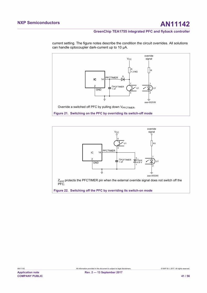
NXP Semiconductors AN11142GreenChip TEA1755 integrated PFC and flyback controller
AN11142 All information provided in this document is subject to legal disclaimers. © NXP B.V. 2017. All rights reserved.
Application note Rev. 2 — 13 September 2017COMPANY PUBLIC 41 / 56
current setting. The figure notes describe the condition the circuit overrides. All solutionscan handle optocoupler dark-current up to 10 μA.
aaa-002539
2
IC
CPCFTIMER1 nF
PFCTIMER D
1
3
1
2
R1.3 MΩ
overridesignalVCC
GND
14
R
U1 U1
Override a switched off PFC by pulling down VPFCTIMER.
Figure 21. Switching on the PFC by overriding its switch-off mode
aaa-005295
2
ICPFCTIMER
4
3
3
1
1
2
overridesignalVCC
GND
14
CPCFTIMER1 nF
R1U1
U1Zprot6.8 V
Zprot protects the PFCTIMER pin when the external override signal does not switch off thePFC.
Figure 22. Switching off the PFC by overriding its switch-on mode

NXP Semiconductors AN11142GreenChip TEA1755 integrated PFC and flyback controller
AN11142 All information provided in this document is subject to legal disclaimers. © NXP B.V. 2017. All rights reserved.
Application note Rev. 2 — 13 September 2017COMPANY PUBLIC 42 / 56
5.3 Flyback protection mode
5.3.1 Short-circuit on the FBCTRL pinIf the FBCTRL pin is shorted to ground, switching of the flyback controller is inhibited.
5.3.2 Open FBCTRL pinAs shown in Figure 23 , the FBCTRL pin is connected to an internal 7 V voltage sourcevia an internal 13.2 kΩ resistor. When the voltage on the FBCTRL pin exceeds 5.5 V, thisconnection is disabled. The FBCTRL pin is biased with an internal 29 μA current source.When the voltage on the FBCTRL pin > Vto(FBCTRL) (7.7 V), a fault is assumed. Flybackand PFC switching is blocked and the controller:
• TEA1755T: enters the safe restart mode• TEA1755LT: triggers the latched protection
When the controller is blocked, an internal switch pulls the FBCTRL pin down.
5.3.3 Time-out flyback control loopA timeout function can be created to protect against an output short-circuit at initial start-up or against an open control loop situation. This feature is made when a resistor ismounted in series with a capacitor between the FBCTRL pin and ground. Triggering thetimeout protection generates:
• TEA1755T: a safe restart• TEA1755LT: a latched protection
When the voltage on the FBCTRL pin > 5.5 V (see Figure 23), the switch in series withthe 13.2 kΩ resistor is opened. The FBCTRL pin and therefore the RC combination isbiased with a 29 μA current source (Ito(FBCTRL)).
When the voltage on the FBCTRL pin > 7.75 V, flyback and PFC switching is blockedand the controller enters the relevant protection mode. The resistor and capacitor areboth used to set the time delay required to reach 7.75 V on the FBCTRL pin. The resistoris also necessary to separate the relatively large timeout capacitor from the control loopresponse. Use a resistor value ≥ 30 kΩ.
The timeout time tto is calculated using Equation 37:
(37)
Note: dvto(FBCTRL) value 2.25 V in Equation 37 is related to Vto(FBCTRL), it is the trip valueminus enable value: 7.75 V − 5.5 V = 2.25 V.
An example based on the following assumptions:
• R24 = 39 kΩ• C16 = 330 nF
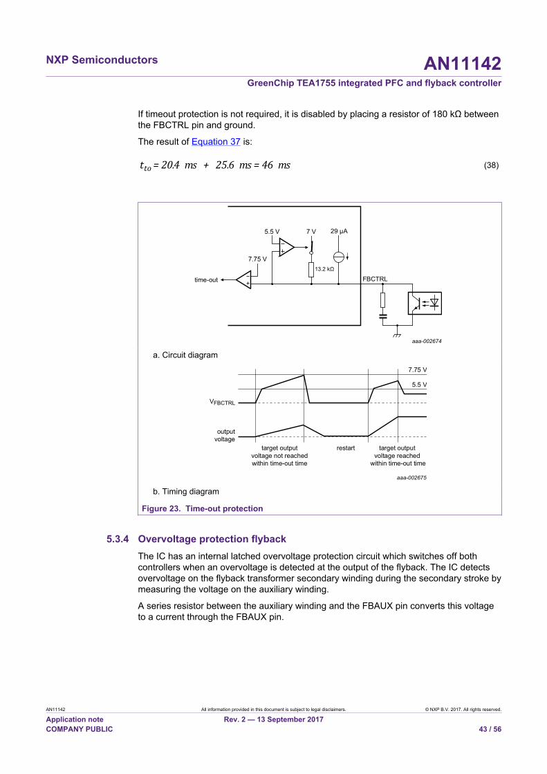
NXP Semiconductors AN11142GreenChip TEA1755 integrated PFC and flyback controller
AN11142 All information provided in this document is subject to legal disclaimers. © NXP B.V. 2017. All rights reserved.
Application note Rev. 2 — 13 September 2017COMPANY PUBLIC 43 / 56
If timeout protection is not required, it is disabled by placing a resistor of 180 kΩ betweenthe FBCTRL pin and ground.
The result of Equation 37 is:
(38)
aaa-002674
FBCTRL
29 µA
13.2 kΩ
7 V5.5 V
7.75 V
time-out
a. Circuit diagram
aaa-002675
7.75 V
5.5 V
VFBCTRL
outputvoltage
target outputvoltage reached
within time-out time
restarttarget outputvoltage not reachedwithin time-out time
b. Timing diagram
Figure 23. Time-out protection
5.3.4 Overvoltage protection flybackThe IC has an internal latched overvoltage protection circuit which switches off bothcontrollers when an overvoltage is detected at the output of the flyback. The IC detectsovervoltage on the flyback transformer secondary winding during the secondary stroke bymeasuring the voltage on the auxiliary winding.
A series resistor between the auxiliary winding and the FBAUX pin converts this voltageto a current through the FBAUX pin.

NXP Semiconductors AN11142GreenChip TEA1755 integrated PFC and flyback controller
AN11142 All information provided in this document is subject to legal disclaimers. © NXP B.V. 2017. All rights reserved.
Application note Rev. 2 — 13 September 2017COMPANY PUBLIC 44 / 56
IC
ROVP = R23
ROPP = R23 + R23A
C13
D5
D_output
T1
secondaryauxiliary
primary
R23 R23A
D23A
019aab496
GND
FBAUX
VCC
2
1
4
Figure 24. Flyback OVP and OPP circuit
When a 300 μA current Iovp(FBAUX) is applied to the FBAUX pin, the IC detects anovervoltage. An internal integrator filters noise and voltage spikes. The output of theintegrator is used as an input for a counter. The counter has been added as an extra filterto prevent false OVP detection which can occur during ESD or lightning events.
If the integrator detects an overvoltage, the counter increases its value by one. If anotherovervoltage is detected during the next switching cycle, the counter increases its valueby one again. If no overvoltage is detected during the next switching cycle, the countersubtracts its value by two. (The minimum value is zero.) If the value reaches six, the ICassumes a true overvoltage and activates the latched protection. Both converters areswitched off immediately and VCC starts cycling between Vth(UVLO) and Vstartup without arestart.
Switching off the mains input voltage and then switching on again, triggers the fast-latchreset circuit and resets the latch.
Resistor Rovp sets the OVP level:
(39)
Where:
• Ns is the number of turns on the secondary winding.• Naux is the number of turns on the flyback transformer auxiliary winding.• Vclamp(FBAUX) is the FBAUX pin positive clamp voltage.• Vf(D23A) is the forward voltage of D23A at a current of 300 μA.• VO is the output voltage• Vf is the forward voltage across the secondary diode
Take the tolerances on Iovp(FBAUX) into account for the Vovp(VOSENSE) level calculation toavoid OVP triggering during normal operation.

NXP Semiconductors AN11142GreenChip TEA1755 integrated PFC and flyback controller
AN11142 All information provided in this document is subject to legal disclaimers. © NXP B.V. 2017. All rights reserved.
Application note Rev. 2 — 13 September 2017COMPANY PUBLIC 45 / 56
5.3.5 OverPower Protection (OPP)The maximum power that the flyback can support depends on its input voltage. A higherinput voltage allows more output power which can result in more stress during faultconditions. The OPP circuit is implemented to limit the output power to a predefinedvalue at higher input voltages. Triggering the OPP circuit results in activation of thetimeout protection (see Section 5.3.3 for more information).
The design of the circuit starts with calculating the required flyback input voltage thatmatches the predefined OPP level. Equation 40 shows the calculation
(40)
Where:
• N is the turn ratio between primary turns and secondary windings of the flybacktransformer
• Lp is the primary inductances of the flyback transformer• Isat is the calculated maximum peak current• VO is the output voltage of the flyback• Vf is forward voltage across the secondary diode (or conducting MOSFET)• Popp is the requested maximum output power of the flyback• tvalley is the measured valley time• ηfb is the efficiency of the flyback. Use relatively high values, such as 0.94 to 0.96
The example is based on the following assumptions:
• N = 5.3333 (see Section 5.1.4.2)• Isat = 4.715 A (see Section 5.1.4.1)• VO = 19.5 V (see Section 5.1.2)• Vf = 0.1 V (see Section 5.1.2)• Popp = 131.3 W; the assumed and preferred OPP level of the flyback• tvalley = 1.1 μs (see Section 5.1.4.2)• ηfb = 0.95 (see Section 5.1.3)
Using these values in Equation 40 results in: Vbulk(opp)min = 143.4 V (DC).
The preferred OPP output power level is almost independent of the line voltage whenVbulk(opp)min < Vbulk(PCF)low. Refer to Section 4.1.1 for more information about Vbulk(PCF)low.Keep a margin of 50 V between Vbulk(PCF)low and Vbulk(opp)min. A transformer running veryclose to saturation has a negative effect on the tolerance of the OPP circuit. Using atleast a margin of 50 V minimizes this effect.
During the flyback primary stroke, the input voltage is sensed by measuring the currentdrawn from the FBAUX pin. A resistor, placed between the flyback transformer auxiliarywinding and the FBAUX pin, converts the voltage to the current IFBAUX. The IC uses thecurrent information to reduce the setting of the maximum flyback peak current measuredthrough the FBSENSE pin.
See Figure 24 for the limitation of the maximum VFBSENSE level as a function of IFBAUX.
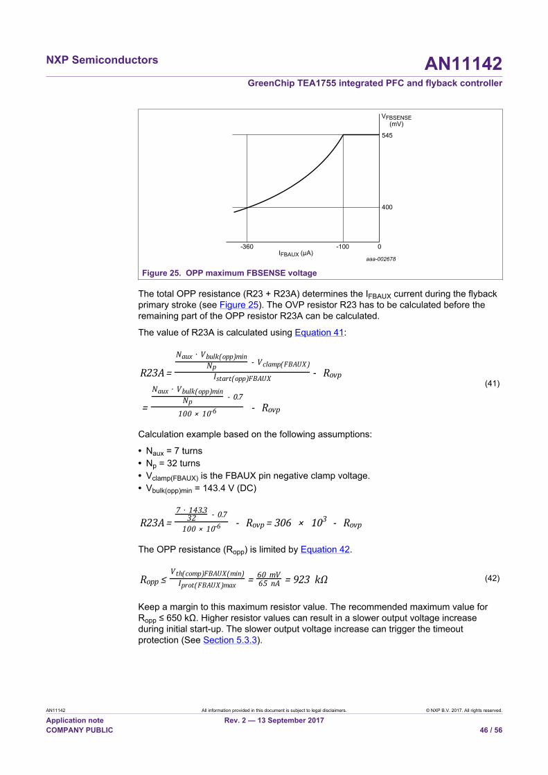
NXP Semiconductors AN11142GreenChip TEA1755 integrated PFC and flyback controller
AN11142 All information provided in this document is subject to legal disclaimers. © NXP B.V. 2017. All rights reserved.
Application note Rev. 2 — 13 September 2017COMPANY PUBLIC 46 / 56
-360 0-100
aaa-002678
545
400
IFBAUX (µA)
VFBSENSE(mV)
Figure 25. OPP maximum FBSENSE voltage
The total OPP resistance (R23 + R23A) determines the IFBAUX current during the flybackprimary stroke (see Figure 25). The OVP resistor R23 has to be calculated before theremaining part of the OPP resistor R23A can be calculated.
The value of R23A is calculated using Equation 41:
(41)
Calculation example based on the following assumptions:
• Naux = 7 turns• Np = 32 turns• Vclamp(FBAUX) is the FBAUX pin negative clamp voltage.• Vbulk(opp)min = 143.4 V (DC)
The OPP resistance (Ropp) is limited by Equation 42.
(42)
Keep a margin to this maximum resistor value. The recommended maximum value forRopp ≤ 650 kΩ. Higher resistor values can result in a slower output voltage increaseduring initial start-up. The slower output voltage increase can trigger the timeoutprotection (See Section 5.3.3).

NXP Semiconductors AN11142GreenChip TEA1755 integrated PFC and flyback controller
AN11142 All information provided in this document is subject to legal disclaimers. © NXP B.V. 2017. All rights reserved.
Application note Rev. 2 — 13 September 2017COMPANY PUBLIC 47 / 56
6 Summary of calculations for flyback adjustment
See Section 1.3 application schematics for component reference numbers.
C10
FBSENSER16
Lp
Q2
Rsense
Rcomp
C23
R16A
FBDRIVERRSERIES = R17 + R16
Vi (DC)
R17
T1
Coutput
Doutput
019aaa039
Iadj(FBSENSE)
FBSENSE has two internal reference levels:(1) Vstart(soft)fb = 545 mV at dV/dt = 0 mV/μs(2) Vsense(fb)min = 232 mV at dV/dt = 0 mV/μs
a. Most important components for adjusting the flyback in the application
(1)
(2)
(3)
(4)
019aaa041
PO (W)75 15513511595
400
600
800
Lp(µH)
200
(5)
Lp as a function of POAssumptions: Minimum voltage across Cbulk (C3) is approximately 100 V (DC) at 50 % of thenominal output power.(1) N × (VO + Vf) = 80 V(2) N × (VO + Vf) = 92 V(3) N × (VO + Vf) = 104 V(4) N × (VO + Vf) = 118 V(5) N × (VO + Vf) = 130 V
b. Indication of the maximum inductance value, related to output power and N × (VO + Vf)
Figure 26. Most important components and maximum inductance value for adjusting theflyback in the application

NXP Semiconductors AN11142GreenChip TEA1755 integrated PFC and flyback controller
AN11142 All information provided in this document is subject to legal disclaimers. © NXP B.V. 2017. All rights reserved.
Application note Rev. 2 — 13 September 2017COMPANY PUBLIC 48 / 56
Step 1: Use the graph in Figure 26 to determine an indication for the maximum primaryinductance value or use Equation 43.
(43)
Step 2: Select a transformer and calculate the saturation current:
(44)
Step 3: Calculate the required peak current through the flyback transformer. Calculatethis value at nominal output power in combination with the minimum Vbulk and when thePFC is operating at maximum peak output power. Calculate using both values for Ipk(max)but only use the highest value of these two parameters.
A common rule is that Isat > Ipk(max). Selecting the higher Isat value for Ipk(max) preventstransformer saturation and allows a power margin. In general, the calculation is carriedout using Ipk(max) = Isat.
(45)
Where:
• a = N × Vi(DC)min × Lp• b = −2 × IO × Lp × {N × (VO + Vf) + Vi(DC)min}• c = −2 × IO × tvalley × N × Vi(DC)min × (VO + Vf)
Step 4: Calculate Ipk(min) (related to switching off the PFC):
(46)
ηfb is the flyback efficiency. Use a relatively high value, for example, approximately 0.94to 0.96.
Step 5: Calculate the value of Rsense:
(47)
Step 6: Calculate the value of Rseries:
(48)
The Rseries resistance comprises two components, R16 and R17. The common value forR17 is between 820 Ω and 1.2 kΩ. A typical value that is used often is 1 kΩ.
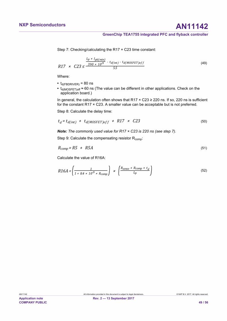
NXP Semiconductors AN11142GreenChip TEA1755 integrated PFC and flyback controller
AN11142 All information provided in this document is subject to legal disclaimers. © NXP B.V. 2017. All rights reserved.
Application note Rev. 2 — 13 September 2017COMPANY PUBLIC 49 / 56
Step 7: Checking/calculating the R17 × C23 time constant:
(49)
Where:
• td(FBDRIVER) = 80 ns• td(MOSFET)off ≈ 60 ns (The value can be different in other applications. Check on the
application board.)
In general, the calculation often shows that R17 × C23 ≥ 220 ns. If so, 220 ns is sufficientfor the constant R17 × C23. A smaller value can be acceptable but is not preferred.
Step 8: Calculate the delay time:
(50)
Note: The commonly used value for R17 × C23 is 220 ns (see step 7).
Step 9: Calculate the compensating resistor Rcomp:
(51)
Calculate the value of R16A:
(52)

NXP Semiconductors AN11142GreenChip TEA1755 integrated PFC and flyback controller
AN11142 All information provided in this document is subject to legal disclaimers. © NXP B.V. 2017. All rights reserved.
Application note Rev. 2 — 13 September 2017COMPANY PUBLIC 50 / 56
7 PCB layout considerations
A good layout is an important part of the final design. It minimizes many kinds ofdisturbances and makes the overall performance more robust with less risk of EMI.Guidelines for the improvement of the layout of the PCB are as follows:
• Separate large signal grounds from small signal grounds (see Figure 28). A triangularsymbol indicates small signal grounds. All other ground symbols are related to largesignal grounds
• Make the print area within the indicated large signal loops (see Figure 28) as small aspossible. Each indicated large signal loop has its own color. Make the copper tracks asshort and wide as possible
• The connection between both MOSFETs (PFC and flyback) and the IC driver outputsmust be as short as possible (green line in Figure 28). Use wide tracks. Increasethe distance between the copper tracks and/or preferably using a separate guidedground track for both connections minimizes the coupling between the PFCDRIVERand FBDRIVER. A circuit diagram according to Figure 27 can be added in case it isimpossible to locate the MOSFET and IC close to each other.
• The power ground and small signal ground are only connected with one short coppertrack (make this track as short and as wide as possible). Preferably it should becomeone spot (connection between ground 4a and ground 6a, shown as a green line inFigure 28)
• Use a ground shield underneath the IC, connect this ground shield to the GND pin ofthe IC
• Connect all series connected resistors that are fixed to an IC pin as close as possible tothat pin
• Connect heatsinks which are connected to the component nearest correspondingground signal. Make this connection as short as possible. Connect the heat sink ofdiode bridge BD1 to ground 1, Q1 to 4 and Q2 to 4b. In typical applications, all threecomponents are often mounted on a single heat sink. If so, make one wide coppertrack that connects all three grounds to each other. Also combine in this copper trackground 2
• Connect the grounds of 6b to each other• Make a local "star ground" from ground 6a, 6b, 6c, and 7. Ground 6a is the middle of
the star and is connected to the GND pin (the ground of the IC)• Grounds marked 7 do not have to be a star ground• Place the Y-capacitor across grounds 1 and 8. Use one copper track, separated
from all others for this connection. Alternatively in a typical application setup, use theheatsinks connection copper track for this purpose.
• Place C4, C15, C23, and C22 (in order of priority) as close as possible to the IC.Reduce coupling between the PFC switching signals (PFC driver and PFCAUX) andthe flyback sense signals (FBSENSE and FBCTRL) as much as possible. The couplingreduction minimizes the risk of electromagnetic interference and audible noise
• Figure 28 shows an overview of the hierarchy of the different grounds at the bottom• Connect the anode of the TL431 (ground 8) to ground 9 using one special separate
connecting copper track. Minimize all other currents in this special track. Make theconnection as close as possible to the output
• Place the TEA1792 close to the power MOSFET Q4• Connect the ground of the TEA1792 directly to a wide and short copper track to the
source of Q4
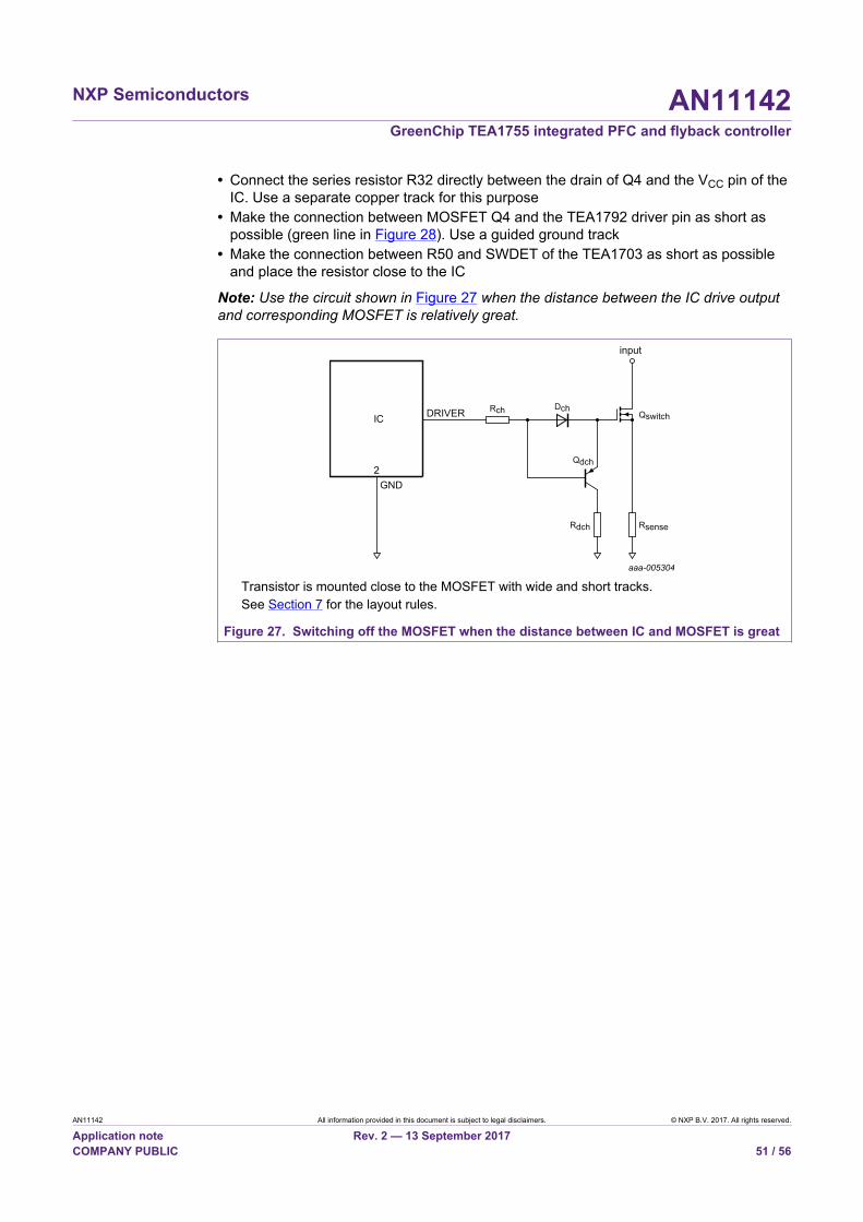
NXP Semiconductors AN11142GreenChip TEA1755 integrated PFC and flyback controller
AN11142 All information provided in this document is subject to legal disclaimers. © NXP B.V. 2017. All rights reserved.
Application note Rev. 2 — 13 September 2017COMPANY PUBLIC 51 / 56
• Connect the series resistor R32 directly between the drain of Q4 and the VCC pin of theIC. Use a separate copper track for this purpose
• Make the connection between MOSFET Q4 and the TEA1792 driver pin as short aspossible (green line in Figure 28). Use a guided ground track
• Make the connection between R50 and SWDET of the TEA1703 as short as possibleand place the resistor close to the IC
Note: Use the circuit shown in Figure 27 when the distance between the IC drive outputand corresponding MOSFET is relatively great.
Qdch
input
QswitchDch
RsenseRdch
IC DRIVER Rch
GND2
aaa-005304
Transistor is mounted close to the MOSFET with wide and short tracks.See Section 7 for the layout rules.
Figure 27. Switching off the MOSFET when the distance between IC and MOSFET is great

NXP Semiconductors AN11142GreenChip TEA1755 integrated PFC and flyback controller
AN11142 All information provided in this document is subject to legal disclaimers. © NXP B.V. 2017. All rights reserved.
Application note Rev. 2 — 13 September 2017COMPANY PUBLIC 52 / 56
large signal current loop
large signal current loop
large signal current loop
+mainsinlet
C17
C18C19
U1PFCTIMER
GN
D
LATC
H
VIN
SEN
SE
HV
S
VO
SEN
SE
FBD
RIV
ER
FBSE
NSE
HV
VCC
PFCSENSE
PFCDRIVER
PFCAUX
C20C21C22C24 R4
R25R26
RT2NTC
C14
C10
C23C4R7
R10C6
R11
R27
R3
R12
R9
C5
C2C1
BD1LF2LF1
F1
CX1
R1
R2
D1 BC1
R14
R31
R43
R42
R13
D4
D3
Q2
R18
R19
R15
R17
R6B
R6
R5A
Q8
Q9
R5
R16 R16A
Q1R8
D2
7
1
9
12
IC
C13
FBCTRL
FBAUX
PFCCOMP
R23A
R23
D23AD5
R22
R45
C9
C8C3
L2L1
4
14
11
12
8 7
15 9 13 10 16 1
2 5
3
6
aaa-005268
1
2 3 6c4a
6b
44b
7 7 7
6b6b
6a
77 7 7 7 7 7 7 7 7
6b
1 3
4
4a 4b 8 9
6a 6b
6c7
2
- A
B
C
D
E
F
U2A-1
4
3
switch signal
switch signal
Figure 28. PCB layout considerations (part 1)

NXP Semiconductors AN11142GreenChip TEA1755 integrated PFC and flyback controller
AN11142 All information provided in this document is subject to legal disclaimers. © NXP B.V. 2017. All rights reserved.
Application note Rev. 2 — 13 September 2017COMPANY PUBLIC 53 / 56
large signal current loop
large signal current loop
large signal current loop
T1
5
1
4
2
6
019aab801
CY1 BC2
U3VCC
C30
R30
Q4
R32
R33 C31
D30113
4
2
5
DR
IVE
R
SRS
ENS
E
n.c.
6 1GND
SELREG TEA1792
8
8
9
8
7
81
C53
D52
Q7
R54R52
R50
R51
R53
1
2
C15
C16
D50
C27
U2A-2
L4
C28C52C51C50
C29
L3
7, 8
9, 10
Vout+
U5VSENSE
3 1
2
6
5
4OPTO
GND
VCC
SWDET
PSENSE TEA1703
R35
R36
C34
R56
R34R37
R38
1
2U2-1
4
3
U2-2
U4
R55
C35
R24
R57
Vout-
A
B
C
D
E
F
Figure 29. PCB layout considerations (part 2)
NXP Semiconductors AN11142GreenChip TEA1755 integrated PFC and flyback controller
AN11142 All information provided in this document is subject to legal disclaimers. © NXP B.V. 2017. All rights reserved.
Application note Rev. 2 — 13 September 2017COMPANY PUBLIC 54 / 56
8 AbbreviationsTable 7. AbbreviationsAcronym DescriptionBM Burst Mode
DCM Discontinuous Conduction Mode
EMI ElectroMagnetic Interference
FR Frequency Reduction
HV High Voltage
MHR Mains Harmonics Reduction
OCP OverCurrent Protection
OTP OverTemperature Protection
OVP OverVoltage Protection
PCB Printed-Circuit Board
PFC Power Factor Converter/Controller/Correction
QR Quasi-Resonant
SMPS Switched Mode Power Supply
9 References
1 TEA1755T data sheet HV start-up DCM/QR flyback controller with integrated DCM/QR PFC controller; 2015, NXP Semiconductors
2 TEA1755LT data sheet HV start-up DCM/QR flyback controller with integrated DCM/QR PFC controller; 2015, NXP Semiconductors
3 UM10514 user manual Notebook adapter using the TEA1755; 2016, NXPSemiconductors
TEA1755T
HV start-up DCM/QR flyback controller with integrated DCM/QR PFC controller; 2015,NXP Semiconductors
TEA1755LT
HV start-up DCM/QR flyback controller with integrated DCM/QR PFC controller; 2015,NXP Semiconductors
UM10514
Notebook adaptor using the TEA1755; 2016, NXP Semiconductors

NXP Semiconductors AN11142GreenChip TEA1755 integrated PFC and flyback controller
AN11142 All information provided in this document is subject to legal disclaimers. © NXP B.V. 2017. All rights reserved.
Application note Rev. 2 — 13 September 2017COMPANY PUBLIC 55 / 56
10 Legal information
10.1 DefinitionsDraft — The document is a draft version only. The content is still underinternal review and subject to formal approval, which may result inmodifications or additions. NXP Semiconductors does not give anyrepresentations or warranties as to the accuracy or completeness ofinformation included herein and shall have no liability for the consequencesof use of such information.
10.2 DisclaimersLimited warranty and liability — Information in this document is believedto be accurate and reliable. However, NXP Semiconductors does notgive any representations or warranties, expressed or implied, as to theaccuracy or completeness of such information and shall have no liabilityfor the consequences of use of such information. NXP Semiconductorstakes no responsibility for the content in this document if provided by aninformation source outside of NXP Semiconductors. In no event shall NXPSemiconductors be liable for any indirect, incidental, punitive, special orconsequential damages (including - without limitation - lost profits, lostsavings, business interruption, costs related to the removal or replacementof any products or rework charges) whether or not such damages are basedon tort (including negligence), warranty, breach of contract or any otherlegal theory. Notwithstanding any damages that customer might incur forany reason whatsoever, NXP Semiconductors’ aggregate and cumulativeliability towards customer for the products described herein shall be limitedin accordance with the Terms and conditions of commercial sale of NXPSemiconductors.
Right to make changes — NXP Semiconductors reserves the right tomake changes to information published in this document, including withoutlimitation specifications and product descriptions, at any time and withoutnotice. This document supersedes and replaces all information supplied priorto the publication hereof.
Suitability for use — NXP Semiconductors products are not designed,authorized or warranted to be suitable for use in life support, life-critical orsafety-critical systems or equipment, nor in applications where failure ormalfunction of an NXP Semiconductors product can reasonably be expectedto result in personal injury, death or severe property or environmentaldamage. NXP Semiconductors and its suppliers accept no liability forinclusion and/or use of NXP Semiconductors products in such equipment orapplications and therefore such inclusion and/or use is at the customer’s ownrisk.
Applications — Applications that are described herein for any of theseproducts are for illustrative purposes only. NXP Semiconductors makesno representation or warranty that such applications will be suitablefor the specified use without further testing or modification. Customersare responsible for the design and operation of their applications andproducts using NXP Semiconductors products, and NXP Semiconductorsaccepts no liability for any assistance with applications or customer product
design. It is customer’s sole responsibility to determine whether the NXPSemiconductors product is suitable and fit for the customer’s applicationsand products planned, as well as for the planned application and use ofcustomer’s third party customer(s). Customers should provide appropriatedesign and operating safeguards to minimize the risks associated withtheir applications and products. NXP Semiconductors does not accept anyliability related to any default, damage, costs or problem which is basedon any weakness or default in the customer’s applications or products, orthe application or use by customer’s third party customer(s). Customer isresponsible for doing all necessary testing for the customer’s applicationsand products using NXP Semiconductors products in order to avoid adefault of the applications and the products or of the application or use bycustomer’s third party customer(s). NXP does not accept any liability in thisrespect.
Export control — This document as well as the item(s) described hereinmay be subject to export control regulations. Export might require a priorauthorization from competent authorities.
Evaluation products — This product is provided on an “as is” and “with allfaults” basis for evaluation purposes only. NXP Semiconductors, its affiliatesand their suppliers expressly disclaim all warranties, whether express,implied or statutory, including but not limited to the implied warranties ofnon-infringement, merchantability and fitness for a particular purpose. Theentire risk as to the quality, or arising out of the use or performance, of thisproduct remains with customer. In no event shall NXP Semiconductors, itsaffiliates or their suppliers be liable to customer for any special, indirect,consequential, punitive or incidental damages (including without limitationdamages for loss of business, business interruption, loss of use, loss ofdata or information, and the like) arising out the use of or inability to usethe product, whether or not based on tort (including negligence), strictliability, breach of contract, breach of warranty or any other theory, even ifadvised of the possibility of such damages. Notwithstanding any damagesthat customer might incur for any reason whatsoever (including withoutlimitation, all damages referenced above and all direct or general damages),the entire liability of NXP Semiconductors, its affiliates and their suppliersand customer’s exclusive remedy for all of the foregoing shall be limited toactual damages incurred by customer based on reasonable reliance up tothe greater of the amount actually paid by customer for the product or fivedollars (US$5.00). The foregoing limitations, exclusions and disclaimersshall apply to the maximum extent permitted by applicable law, even if anyremedy fails of its essential purpose.
Translations — A non-English (translated) version of a document is forreference only. The English version shall prevail in case of any discrepancybetween the translated and English versions.
10.3 TrademarksNotice: All referenced brands, product names, service names andtrademarks are the property of their respective owners.
GreenChip — is a trademark of NXP B.V.

NXP Semiconductors AN11142GreenChip TEA1755 integrated PFC and flyback controller
Please be aware that important notices concerning this document and the product(s)described herein, have been included in section 'Legal information'.
© NXP B.V. 2017. All rights reserved.For more information, please visit: http://www.nxp.comFor sales office addresses, please send an email to: [email protected]
Date of release: 13 September 2017Document identifier: AN11142
Contents1 Introduction ......................................................... 31.1 Scope .................................................................31.2 The TEA1755 GreenChip controller .................. 31.2.1 Key features ...................................................... 31.2.2 System features .................................................41.2.3 PFC features ..................................................... 41.2.4 Flyback features ................................................ 41.3 Application schematic ........................................ 52 Pin description .................................................... 73 System description and calculation ................103.1 PFC and flyback start conditions ..................... 103.2 Initial start-up sequence .................................. 103.3 VCC cycle in safe restart mode .......................113.4 Mains voltage sensing and brownout .............. 123.4.1 Discharging the mains input capacitor .............123.4.2 Brownout voltage adjustment .......................... 133.4.3 Minimizing the influence of the dark-current
of the optocoupler ............................................133.5 Internal OverTemperature Protection (OTP) ....143.6 LATCH pin ....................................................... 143.7 Fast-latch reset ................................................154 PFC description and calculation ..................... 164.1 PFC output power and voltage control ............ 164.1.1 Setting the PFC output voltage ........................184.1.2 Calculation of the PFC soft-start and soft-
stop components ............................................. 204.2 PFC demagnetizing and valley detection .........204.2.1 Design of the PFCAUX winding and circuit ......214.3 PFC protection modes .....................................224.3.1 VOSENSE overvoltage protection ................... 224.3.2 VOSENSE open and short pin detection ......... 224.3.3 VINSENSE open pin detection ........................ 224.3.4 Overcurrent protection ..................................... 235 Flyback description and calculation ............... 245.1 Flyback output power control ...........................245.1.1 Four TEA1755 operation modes ......................255.1.1.1 Quasi-resonant mode ...................................... 255.1.1.2 Discontinuous conduction mode ......................265.1.1.3 Frequency reduction mode and PFC switch
on/switch off control .........................................265.1.1.4 Burst mode ...................................................... 275.1.1.5 VCC undervoltage protection during burst
mode ................................................................285.1.2 The relationship between inductance value
and the PFC hysteresis ................................... 285.1.3 Relationship between Ipk(min) and the
required PFC(swon)/PFC(swoff) level ............. 315.1.4 The influence of Rsense and the R16/R17
series resistance ..............................................335.1.4.1 Calculating the flyback transformer
saturation current Isat ......................................335.1.4.2 Calculation of Ipk(max) for flyback operating
in Quasi-resonant mode .................................. 34
5.1.4.3 Calculation of the current sense resistorRsense .............................................................35
5.1.4.4 Calculation of the series resistance R16 andR17 .................................................................. 35
5.1.5 Calculation of the delay compensationresistors Rcomp and R16A ..............................36
5.1.6 Calculation of flyback soft start components .... 385.2 Two PFCTIMER pin options ............................ 385.2.1 Option 1: adjustable PFC(swoff) time .............. 385.2.2 Option 2: Overriding the PFC(swon) and
PFC(swoff) functions ....................................... 405.3 Flyback protection mode ................................. 425.3.1 Short-circuit on the FBCTRL pin ......................425.3.2 Open FBCTRL pin ...........................................425.3.3 Time-out flyback control loop ...........................425.3.4 Overvoltage protection flyback ........................ 435.3.5 OverPower Protection (OPP) ...........................456 Summary of calculations for flyback
adjustment ......................................................... 477 PCB layout considerations .............................. 508 Abbreviations .................................................... 549 References ......................................................... 5410 Legal information ..............................................55