graphene–si cmos oscillators
TRANSCRIPT

Nanoscale
PAPER
Cite this: Nanoscale, 2019, 11, 3619
Received 27th September 2018,Accepted 25th January 2019
DOI: 10.1039/c8nr07862a
rsc.li/nanoscale
Graphene–Si CMOS oscillators†
Carlo Gilardi,a Paolo Pedrinazzi, a Kishan Ashokbhai Patel,a Luca Anzi, a
Birong Luo,b Timothy J. Booth, b Peter Bøggild b and Roman Sordan *a
Graphene field-effect transistors (GFETs) offer a possibility of exploiting unique physical properties of gra-
phene in realizing novel electronic circuits. However, graphene circuits often lack the voltage swing and
switchability of Si complementary metal–oxide-semiconductor (CMOS) circuits, which are the main
building block of modern electronics. Here we introduce graphene in Si CMOS circuits to exploit favorable
electronic properties of both technologies and realize a new class of simple oscillators using only a GFET,
Si CMOS D latch, and timing RC circuit. The operation of the two types of realized oscillators is based on
the ambipolarity of graphene, i.e., the symmetry of the transfer curve of GFETs around the Dirac point.
The ambipolarity of graphene also allowed to turn the oscillators into pulse-width modulators (with a
duty cycle ratio ∼1 : 4) and voltage-controlled oscillators (with a frequency ratio ∼1 : 8) without any circuit
modifications. The oscillation frequency was in the range from 4 kHz to 4 MHz and limited only by the
external circuit connections, rather than components themselves. The demonstrated graphene–Si CMOS
hybrid circuits pave the way to the more widespread adoption of graphene in electronics.
1 Introduction
The development of graphene electronic circuits is mostlyguided by the state-of-the-art circuit design of Si transistortechnology. Such circuits try to exploit very large mobility1 andsaturation velocity2 of charge carriers in graphene to match theperformance of the corresponding Si circuits. However, thisapproach has not yielded satisfactory results so far because gra-phene does not have a bandgap3–5 and therefore graphene field-effect transistors (GFETs) exhibit insufficient drain current satur-ation6,7 and cannot be turned off. For instance, graphene ringoscillators8 can indeed match the speed of the Si CMOS ringoscillators but only at the expense of considerable static powerdissipation, which is unacceptable in highly-integrated digitalcircuits.9 If graphene were to find applications in electronics, itsunique properties, such as flexibility,10 transparency,11 and ambi-polarity,3 should be exploited to achieve either novel functional-ity or the same functionality with fewer transistors, rather thanto mimic Si circuits. One of the truly unique electronic propertiesof graphene not exhibited by conventional semiconductors isambipolarity. The ambipolarity of graphene has been used in
the past to realize very simple logic gates12 and frequency multi-pliers.13 However, the logic gates suffered from large power dissi-pation and the mixers from large conversion loss, renderingboth types of circuits unusable in realistic applications.
Here we demonstrate a novel class of graphene–Si CMOS cir-cuits that exploit the ambipolarity of graphene to simplify thecircuit and provide additional functionality. To illustrate theconcept, we experimentally demonstrate two types of simpleoscillators comprising just a GFET, a Si CMOS D latch, and atiming RC circuit. The D latch provides switching and largevoltage swing for controlling the GFET, while the RC circuit isused to set the oscillation frequency ( fosc). The highestobtained oscillation frequency was fosc = 4.2 MHz, limited onlyby the connections between the used discrete components. Theambipolarity of graphene allows realization of pulse-widthmodulators (PWMs) and voltage-controlled oscillators (VCOs)from the same oscillators, i.e., without any circuit modifi-cations. Oscillating signals with a duty cycle in the range from20% to 80% and maximum-to-minimum frequency ratio of 7.7were obtained in this way. The concept of exploiting favorableelectronic properties of GFETs and Si CMOS is general and canbe realized with any ambipolar material, although graphene ispreferable for high-speed operation.
2 Results
Top-gated GFETs were fabricated from graphene grown bychemical vapor deposition14,15 (CVD) and then transferred to
†Electronic supplementary information (ESI) available: Discussions on the shape ofthe static voltage transfer characteristic of the graphene circuit used in the oscillators,the highest frequency waveforms measured in a parabolic oscillator, and calculatedPWM and VCO characteristics of the oscillators. See DOI: 10.1039/C8NR07862A
aL-NESS, Department of Physics, Politecnico di Milano, Via Anzani 42, 22100 Como,
Italy. E-mail: [email protected]; Tel: +39 031 332 7622bCNG, DTU Nanotech, Department of Micro- and Nanotechnology, Technical University
of Denmark, Ørsted Plads, Building 345C, 2800 Lyngby, Denmark
This journal is © The Royal Society of Chemistry 2019 Nanoscale, 2019, 11, 3619–3625 | 3619
Ope
n A
cces
s A
rtic
le. P
ublis
hed
on 1
1 Fe
brua
ry 2
019.
Dow
nloa
ded
on 2
/25/
2022
4:1
1:48
PM
. T
his
artic
le is
lice
nsed
und
er a
Cre
ativ
e C
omm
ons
Attr
ibut
ion-
Non
Com
mer
cial
3.0
Unp
orte
d L
icen
ce.
View Article OnlineView Journal | View Issue
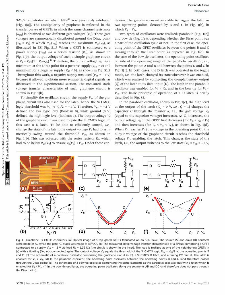
SiO2/Si substrates on which hBN16 was previously exfoliated(Fig. 1(a)). The ambipolarity of graphene is reflected in thetransfer curves of GFETs in which the same channel resistance(Rch) is obtained at two different gate voltages (VG). These gatevoltages are symmetrically distributed around the Dirac point(VG = V0) at which Rch(VG) reaches the maximum Rch(V0), asillustrated in ESI Fig. S1.† When a GFET is connected to apower supply (VSS) via a series resistor (RS), as shown inFig. 1(b), the output voltage of such a simple graphene circuitis VS = VSS/(1 + RS/Rch).
12 Therefore, the output voltage VS has amaximum at the Dirac point for a positive supply (VSS > 0) andminimum for a negative supply (VSS < 0), as shown in Fig. S1.†Throughout this work, a negative supply was used (VSS = −2 V)because it allowed to obtain more symmetric digital signals, asdiscussed in the Experimental section. The measured staticvoltage transfer characteristic of such graphene circuit isshown in Fig. 1(b).
To simplify the oscillator circuit, the supply VSS of the gra-phene circuit was also used for the latch, hence the Si CMOSlogic threshold was Vth ≈ VSS/2 = −1 V. Therefore, VSS = −2 Vdefined the low logic level (Boolean 0), while ground (0 V)defined the high logic level (Boolean 1). The output voltage VSof the graphene circuit was used to gate the Si CMOS logic, inthis case a D latch. To be able to efficiently control, i.e.,change the state of the latch, the output voltage VS had to sym-metrically swing around the threshold Vth, as shown inFig. 1(b). This was adjusted with the series resistor RS, whichhad to be below Rch(V0) to ensure VS(V0) < Vth. Under these con-
ditions, the graphene circuit was able to trigger the latch intwo operating points, denoted by B and C in Fig. 1(b), inwhich VS = Vth.
Two types of oscillators were realized: parabolic (Fig. 1(c))and bow tie (Fig. 1(e)), depending whether the Dirac point wasa part of the oscillation cycle or not. In the first case, the oper-ating point of the GFET oscillates between the points B and Cmoving through the Dirac point, as depicted in Fig. 1(d). Inthe case of the bow tie oscillator, the operating point oscillatesoutside of the operating range of the parabolic oscillator, i.e.,between the points A and B and between the points D and C inFig. 1(f ). In both cases, the D latch was operated in the togglemode, i.e., the latch changed its state whenever it was enabled,which was realized by connecting the complementary output(Q̄) of the latch to its data input (D). The latch in the parabolicoscillator was enabled for VS > Vth and in the bow tie for VS <Vth. The basic principle of operation of a D latch is brieflydescribed in Fig. S2.†
In the parabolic oscillator, shown in Fig. 1(c), the high levelat the output of the latch (VQ = 0 V, i.e., Q = 1) charges thecapacitor C through the resistor R, i.e., the gate voltage VG(equal to the capacitor voltage) increases. As VG increases, theoutput voltage VS of the GFET first decreases (for VB < VG < V0)and then increases (for V0 < VG < VC), as shown in Fig. 1(d).When VG reaches VC (the voltage in the operating point C), theoutput voltage of the graphene circuit reaches the thresholdvoltage Vth enabling the latch. This changes the state of thelatch, i.e., the output switches to the low state (VQ = VSS = −2 V,
Fig. 1 Graphene–Si CMOS oscillators. (a) Optical image of 5 top-gated GFETs fabricated on an hBN flake. The source (S) and drain (D) contactswere made of Au while the gate (G) stack was made of Al/AlOx. (b) The measured static voltage transfer characteristic of a circuit comprising a GFETconnected to a supply VSS = −2 V via load RS = 1.26 kΩ (the circuit is shown in the inset). The load is realized as one of the neighboring GFETs in(a) with a floating (i.e., not connected) gate. The output voltage VS equals the threshold of the Si CMOS logic Vth ≈ VSS/2 at the operating points Band C. (c) The schematic of a parabolic oscillator comprising the graphene circuit in (b), a Si CMOS D latch, and a timing RC circuit. The latch isenabled for VS > Vth. (d) In the parabolic oscillator, the operating point oscillates between the operating points B and C (and therefore passesthrough the Dirac point). (e) The schematic of a bow tie oscillator comprising the same elements as the parabolic oscillator but with a latch which isenabled for VS < Vth. (f ) In the bow tie oscillator, the operating point oscillates along the segments AB and DC (and therefore does not pass throughthe Dirac point).
Paper Nanoscale
3620 | Nanoscale, 2019, 11, 3619–3625 This journal is © The Royal Society of Chemistry 2019
Ope
n A
cces
s A
rtic
le. P
ublis
hed
on 1
1 Fe
brua
ry 2
019.
Dow
nloa
ded
on 2
/25/
2022
4:1
1:48
PM
. T
his
artic
le is
lice
nsed
und
er a
Cre
ativ
e C
omm
ons
Attr
ibut
ion-
Non
Com
mer
cial
3.0
Unp
orte
d L
icen
ce.
View Article Online
i.e., Q = 0) and the capacitor starts discharging through thesame resistor. As VG decreases, VS decreases below thethreshold Vth disabling the latch. With the further decrease ofVG, VS first decreases (for V0 < VG < VC) and then increases (forVB < VG < V0), finally reaching the threshold voltage Vth in theoperating point B. This enables the latch again, which switchesto the high state (Q = 1) and starts charging the capacitor. AsVS decreases, the latch disables and the entire cycle repeatsagain. In this way, the present relaxation oscillator keeps oscil-lating between the operating points B and C.
In the bow tie oscillator, shown in Fig. 1(e), when the latchis in the low state (VQ = VSS = −2 V, i.e., Q = 0), the high state atthe complementary output (Q̄ = 1) charges the capacitor Cthrough the resistor R, and the gate voltage increases to VB, asshown in Fig. 1(f ). As VG increases, the output voltage VS of thegraphene circuit decreases and when it reaches the thresholdVth in the operating point B, the latch is enabled and switchesto the high state (VQ = 0 V, i.e., Q = 1). The sudden increase ofVQ by |VSS| is transferred to the gate voltage VG because thecapacitor voltage is a continuous function of time. As a conse-quence, the oscillator switches to the operating point D inwhich VD = VB + |VSS|. This disables the latch and the low stateat the complementary output (Q̄ = 0) starts discharging thecapacitor and therefore decreasing VG. Consequently, VSdecreases from VD to VC, enabling the latch at the operatingpoint C in which VS = Vth. The latch switches to the low stateagain, instantly decreasing VG by |VSS|. The oscillator thereforeswitches to the operating point A in which VA = VC − |VSS| initi-ating the same cycle again.
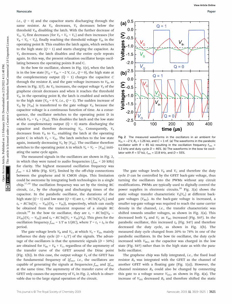
The measured signals in the oscillators are shown in Fig. 2,in which they were tuned to audio frequencies ( fosc < 20 kHz)for clarity. The highest measured oscillation frequency wasfosc = 4.2 MHz (Fig. S3†), limited by the off-chip connectionsbetween the graphene and Si CMOS chips. This limitationcould be overcome by integrating both technologies in a singlechip.17,18 The oscillation frequency was set by the timing RCcircuit, i.e., by the charging and discharging times of thecapacitor. In the parabolic oscillator, the durations of thehigh state (Q = 1) and low state (Q = 0) are t1 = RC ln(VB/VC) andt0 = RC ln((VC − VSS)/(VB − VSS)), respectively, which can easilybe obtained from the transient response of a simple RCcircuit.19 In the bow tie oscillator, they are t1 = RC ln((VB −2VSS)/(VC − VSS)) and t0 = RC ln((VC + VSS)/VB). This gives for theoscillation frequency fosc = 1/T ∝ 1/(RC), where T = t1 + t0 is theperiod.
The gate voltage levels VB and VC, at which VS = Vth, mainlyinfluence the duty cycle (D = t1/T ) of the signals. The advan-tage of the oscillators is that the symmetric signals (D = 50%)are obtained for VSS = VB + VC, regardless of the asymmetry ofthe transfer curve of the GFET around the Dirac point(Fig. 1(b)). In this case, the output voltage VS of the GFET hasthe fundamental frequency of 2fosc, i.e., the oscillators arecapable of generating the signals at frequencies fosc and 2foscat the same time. The asymmetry of the transfer curve of theGFET only causes the asymmetry of VS in Fig. 2, which is obser-vable due to the large signal operation of the circuit.
The gate voltage levels VB and VC and therefore the dutycycle D can be controlled by the GFET back-gate voltage, thusturning the oscillators into the PWMs without any circuitmodifications. PWMs are typically used to digitally control thepower supplies in electronic circuits.20 Fig. 3(a) shows thestatic voltage transfer characteristic VS(VG) at different back-gate voltages (VBG). As the back-gate voltage is increased, asmaller top-gate voltage was required to reach the same carrierdensity in the channel, i.e., the transfer characteristic wasshifted towards smaller voltages, as shown in Fig. 3(a). Thisdecreased both VB and VC as VBG increased (Fig. S4†). In theparabolic oscillator, this increased t0 (Fig. S4†) and thereforedecreased the duty cycle, as shown in Fig. 3(b). Themeasured duty cycle changed from 20% to 78% in one of theparabolic oscillators. In the bow tie oscillator, the duty cycleincreased with VBG, as the capacitor was charged in the lowstate (Fig. S4†) rather than in the high state as with the para-bolic oscillator.
The graphene chip was fully integrated, i.e., the fixed loadresistor RS was integrated with the GFET as the channel ofanother GFET with a floating gate (Fig. 1(a)). However, thechannel resistance RS could also be changed by connectingthis gate to a voltage source VGG, as shown in Fig. 4(a). Theincrease of VGG decreased RS and therefore shifted the static
Fig. 2 The measured waveforms in the oscillators in air ambient forVSS = −2 V, RS = 1.26 kΩ, and C = 1 nF. (a) The waveforms in the parabolicoscillator with R = 85 kΩ resulting in the oscillation frequency fosc =5.3 kHz and duty cycle D = 46%. (b) The waveforms in the bow tie oscil-lator with R = 57 kΩ, fosc = 13.8 kHz, and D = 55%.
Nanoscale Paper
This journal is © The Royal Society of Chemistry 2019 Nanoscale, 2019, 11, 3619–3625 | 3621
Ope
n A
cces
s A
rtic
le. P
ublis
hed
on 1
1 Fe
brua
ry 2
019.
Dow
nloa
ded
on 2
/25/
2022
4:1
1:48
PM
. T
his
artic
le is
lice
nsed
und
er a
Cre
ativ
e C
omm
ons
Attr
ibut
ion-
Non
Com
mer
cial
3.0
Unp
orte
d L
icen
ce.
View Article Online

voltage transfer characteristic VS(VG) to smaller output voltagesVS, as shown in the same figure. This decreased VB andincreased VC (Fig. S5†) and therefore increased both t1 and t0in the parabolic oscillators, decreasing their oscillation fre-quency fosc. In this way, the gate voltage VGG was used tocontrol fosc realizing the functionality of a VCO, one of themost used electronic circuits in communications systems.21 Byincreasing VGG, the measured oscillation frequency decreasedfrom 137 to 18 kHz in one of the parabolic oscillators, asshown in Fig. 4(b). In contrast, the increase of VGG decreasedt1 and t0 (Fig. S5†) and therefore increased the oscillation fre-quency in the bow tie oscillators.
3 Discussion
For the same circuit components, the oscillation frequency ofthe bow tie oscillator is higher than that of the parabolic oscil-lator because the operating point of the bow tie oscillator staysonly on one side of the Dirac point during each half period.Assuming a duty cycle of 50% in both oscillators, i.e., VSS =VB + VC, the bow tie oscillator oscillates at twice the frequencyof the parabolic oscillator if VB = 0.742VSS and VC = 0.258VSS.The disadvantage of the bow tie oscillator is that its gatevoltage can overshoot the supply voltage rails at the signal
Fig. 3 PWM functionality obtained by controlling the duty cycle with aback-gate voltage at VSS = −2 V and RS = 708 Ω. (a) The static voltagetransfer characteristics VS(VG) of the graphene circuit shown in the inset,at the back-gate voltages VBG ranging from −12.5 V to 40 V in steps of2.5 V. The intersections between a characteristic and the CMOSthreshold Vth (which are at VG = VB and VG = VC) can be controlled byVBG. For VBG = 0 V, the intersections are at VB ≈ −1 V and VC ≈ −0.5 V. (b)The measured duty cycle D as a function of the applied back-gatevoltage VBG. The insets show the measured waveforms with the largest(D = 78%) and smallest (D = 20%) measured duty cycle. The time rangeof the waveforms is 100 μs and the voltage range is from −2 V to 0 V. Inall measurements R = 17.78 kΩ and C = 0.5 nF.
Fig. 4 VCO functionality obtained by controlling the oscillationfrequency with a gate voltage at VSS = −2 V. (a) The static voltage transfercharacteristics VS(VG) of the graphene circuit shown in the inset fordifferent gate voltages VGG of a load GFET which replaces the seriesresistor RS. VGG ranges from −2.2 V to −1 V in steps of 0.1 V. VGG controlsthe GFET resistance RS and consequently the vertical shift of the transfercharacteristics. The intersections between a characteristic and theCMOS threshold Vth (which are at VG = VB and VG = VC) are thereforecontrolled by VGG. For VGG = −1.8 V, the intersections are at VB ≈ −1.4 Vand VC ≈ −0.6 V. (b) The measured oscillation frequency fosc as a func-tion of the gate voltage VGG. The insets show the measured waveformswith the highest ( fosc = 137 kHz) and lowest ( fosc = 18 kHz) measuredoscillation frequency. The time range of the waveforms is 100 μs and thevoltage range is from −2 V to 0 V. In all measurements R = 10 kΩ andC = 1 nF.
Paper Nanoscale
3622 | Nanoscale, 2019, 11, 3619–3625 This journal is © The Royal Society of Chemistry 2019
Ope
n A
cces
s A
rtic
le. P
ublis
hed
on 1
1 Fe
brua
ry 2
019.
Dow
nloa
ded
on 2
/25/
2022
4:1
1:48
PM
. T
his
artic
le is
lice
nsed
und
er a
Cre
ativ
e C
omm
ons
Attr
ibut
ion-
Non
Com
mer
cial
3.0
Unp
orte
d L
icen
ce.
View Article Online

edges, e.g., |VG| > |VSS| at the falling edge of Q in Fig. 2(b).This could be dangerous for other components in the circuit,primarily the GFET which has the gate voltage breakdown of∼2.9 V. In a bow tie PWM, the largest overshoots are at the twoextremes of the duty cycle.
The present oscillators can be fabricated on a large scalebecause they do not require exfoliated hBN or a global backgate. The exfoliated hBN was used only because of the largedoping of the GFETs on SiO2 in the used batch. Similarly, theglobal backgate was used in PWMs only for demonstration; inrealistic devices this can easily be replaced by a local back gateso that each PWM is individually gated. Control voltages inPWMs and VCOs are typically obtained from the output ofother circuits rather than separate power supplies. Forexample, a VCO is driven by a phase detector in a phase-lockedloop (PLL).21
The demonstrated principle of operation is general, i.e., theother ambipolar materials, e.g., amorphous Si,22 Si nano-wires23 or semiconducting carbon nanotubes,24 could also beused. Although their ambipolarity has been exploited in appli-cations25,26 similar to that of graphene,12 they have not beencombined with Si CMOS logic so far. In contrast to other ambi-polar materials, graphene has much larger carrier mobility1
and saturation velocity2 allowing much faster operation. Thesymmetric band structure of graphene27 (i.e., almost identicalelectron and hole mobilities) also leads to symmetric digitalsignals, which cannot easily be obtained in materials withdifferent electron and hole mobilities.
In terms of the component count, the present oscillatorsare similar to the simplest Si field-effect transistor (FET) oscil-lators, because they were made of only 5 components.However, it should be noted that a gated D latch28 is usuallymade of 10 FETs, resulting in 14 components in the oscillator.The commercial discrete D latches usually comprise morethan 10 FETs because they also provide three-state outputs(which were not used here). For comparison, the simplest con-ventional astable multivibrators with vertical signal edges19
have only 2 FETs, but also 10 other components, bringing thetotal component count to 12. The simplest Si CMOS ring oscil-lators29 have 6 FETs but their oscillation frequency is deter-mined by internal gate delays8,9 rather than a timing RCcircuit. Finally, the simplest Schmitt trigger inverter oscil-lators30 have 8 components. Despite similar component count,the present oscillators provide additional functionalities of thePWMs and VCOs. Compared to graphene ring oscillators,8,9
which have a limited output voltage swing, the output voltageswing in the present oscillators is determined by the Si CMOSpart of the circuit providing rail-to-rail operation.
Although the oscillators use a GFET which cannot beturned off, the static power dissipation is not a critical factorbecause the relaxation oscillators do not spend any time in theidle state and dissipate the dynamic power continuously. Thiscould also be understood from the ratio between the staticpower dissipation of the graphene circuit Ps ∼ VSS
2/(2Rs) anddynamic (switching) power dissipation Pd ∼ foscCVSS
2/2 of thetiming RC circuit. Here it was assumed for simplicity that the
voltage on the capacitor oscillates between 0.25VSS and 0.75VSS(as in Fig. 2(a)) and that the power dissipation of the D latch isnegligible. The ratio Ps/Pd ∼ R/Rs, because fosc ∼ 1/(RC),meaning that for large fosc (i.e., R < Rs), Ps < Pd. For example,R/Rs ∼ 50 in the low-frequency oscillators shown in Fig. 2,but R/Rs ∼ 0.25 in the high-frequency oscillator shown inFig. S3.†
The realized oscillators could be used to provide high-frequency reference required for the signal up/down conver-sion in high frequency transmitters/receivers. The D latch isnot expected to limit the bandwidth of the fully integratedoscillators because high-speed Si CMOS technology is capableof operating at very high serial data rates (up to 120 Gb s−1).31
The realized oscillators could also be used to generate clocksignals for digital data processing which requires the exactclock duty cycle of 50%. In microprocessors, this is typicallyachieved by running a VCO (inside the PLL) at twice the clockfrequency and then dividing the frequency by two.32,33
However, such realizations significantly increase the dynamicpower dissipation and are not practical at very high frequen-cies. Our oscillators offer an alternative solution because bothPWM (duty cycle tuning) and VCO (frequency tuning) are inte-grated in the same circuit.
The integration of graphene with Si CMOS technologyshould be considered in the context of 3D monolithic inte-grated circuits (ICs). Such ICs cannot be easily made in SiCMOS technology due to high temperatures required for thefabrication of each Si CMOS layer in a 3D stack. This problemcan be overcome by stacking other transistor technologies,which do not require high-temperature fabrication, on top ofSi CMOS.34 Alternative transistor technologies also allowrealization of additional functionalities which cannot beobtained with Si CMOS alone.34,35 Graphene is a good candi-date for the integration with Si CMOS in 3D monolithic ICsbecause it can be transferred to a target substrate at roomtemperature.
4 Conclusions
We exploited the symmetry of the transfer characteristics ofGFETs to realize a new class of very simple electronic relax-ation oscillators comprising a GFET, Si CMOS latch, and RCtiming circuit. The difference between the two types of therealized oscillators was in the movement of the operatingpoint, oscillating through the Dirac point in the first typeand jumping over the Dirac point in the second type. Thesimplicity of the oscillators and additional PWM and VCOfunctionalities, obtained without any circuit modifications,stemmed from the ambipolarity of graphene. The switchingand large voltage swing of generated waveforms were pro-vided by Si CMOS logic. The introduction of graphene in SiCMOS logic may prove to be a feasible approach in simplify-ing it and providing additional functionality while at thesame time overcoming barriers to entry of graphene inelectronics.
Nanoscale Paper
This journal is © The Royal Society of Chemistry 2019 Nanoscale, 2019, 11, 3619–3625 | 3623
Ope
n A
cces
s A
rtic
le. P
ublis
hed
on 1
1 Fe
brua
ry 2
019.
Dow
nloa
ded
on 2
/25/
2022
4:1
1:48
PM
. T
his
artic
le is
lice
nsed
und
er a
Cre
ativ
e C
omm
ons
Attr
ibut
ion-
Non
Com
mer
cial
3.0
Unp
orte
d L
icen
ce.
View Article Online

5 ExperimentalhBN was exfoliated on highly p-doped (>1019 cm−3) Si sub-strates with a 300 nm thick top layer of SiO2. The back of the Sisubstrates was metallized and used as a global back-gate, ifneeded. Monocrystalline monolayer graphene was grown byCVD on Cu from the CH4 precursor and then transferred (by awet process) to the same substrates on which hBN was pre-viously exfoliated. The GFETs were patterned by electron-beam(e-beam) lithography using poly(methyl methacrylate) resist.The GFET channels (the channel width W = 5 μm) weredefined by etching graphene in O2 plasma both in parts of thesubstrates covered and uncovered by hBN flakes. This allowedfabrication of a large number of GFETs on hBN (the only selec-tion criteria were the lateral size >5 μm and thickness <50 nmof the hBN flakes) and control GFETs on SiO2 in the samechips.
The rest of the fabrication process was the same in bothcases. Top-gates were patterned first by e-beam lithography fol-lowed by e-beam evaporation of 100 nm of Al. Al oxidized aftera few days in air ambient creating a thin (∼4 nm) native layerof AlOx on all surfaces of Al, including the interface withgraphene.36–40 This formed an AlOx/Al gate stack with a top-gate oxide capacitance8,40 Cox = 1.37 μF cm−2. Source and drainAu contacts (100 nm) were finally fabricated by e-beam litho-graphy and e-beam evaporation. The gate length was L = 1 μm,source-to-drain distance LSD = 1.2 μm (i.e., the access lengthfrom both sides of the gate was 100 nm), and length of thesource and drain contacts was 2 μm.
The oscillators worked both with a positive and negativepower supply. However, we found that a negative supplyallowed more symmetric digital signals at |VSS| ∼ 2 V, i.e., thesignals with a duty cycle closer to 50%. This is because theunbiased GFETs on hBN had the Dirac voltage V0 ≈ −0.5 V,which changed to ≈V0 + VSS/4 when VSS was applied (becauseRch ≈ RS at the Dirac point). The signal symmetry requiresVH − VC = VB − VL, i.e., that the Dirac voltage is approximatelyhalf way between the voltage rails. This means V0 + VSS/4 ≈VSS/2, i.e., VSS ≈ 4V0, which is the reason the supply VSS = −2 Vwas used. The series resistance RS was realized as either anexternal discrete resistor or another GFET with a floating gate.The output voltage swing of the graphene circuit depends onRS, e.g., the highest swing in the parabolic oscillator is
obtained for RS ¼ffiffiffiffiffiffiffiffiffiffiffiffiffiffiffiffiffiffiffiffiffiffiffiffiffiffiffiffiffiffiffiRch V0ð ÞRch VBð Þp
.The GFETs were made on hBN substrate because the lower
|V0| allowed the use of lower supply voltages |VSS|, as describedabove. We also found that GFETs on hBN had much betterlong-term stability than GFETs on SiO2. The same GFETs onhBN were repeatedly measured in the oscillators for monthswithout any apparent degradation of their electrical properties.
The Si CMOS part of the oscillator circuit (including thetiming RC circuit) was built on a breadboard (in low-frequencyoscillators) or printed circuit board (in high-frequency oscil-lators) and connected to the GFET via a FormFactor probestation. The Si CMOS gated D latch was 74HC375AP or74AC573P. The dc characteristics were measured by Keithley
2611A source measure units, while the waveforms weremeasured by Keysight Infiniium DSO9404A oscilloscope andKeysight N2795A and 1158A active probes.
Conflicts of interest
There are no conflicts to declare.
Acknowledgements
This research was supported by the EU H2020 GrapheneFlagship Core 2 Grant No. 785219.
References
1 A. S. Mayorov, R. V. Gorbachev, S. V. Morozov, L. Britnell,R. Jalil, L. A. Ponomarenko, P. Blake, K. S. Novoselov,K. Watanabe, T. Taniguchi and A. K. Geim, Nano Lett.,2011, 11, 2396–2399.
2 V. E. Dorgan, M.-H. Bae and E. Pop, Appl. Phys. Lett., 2010,97, 082112.
3 K. S. Novoselov, A. K. Geim, S. V. Morozov, D. Jiang,Y. Zhang, S. V. Dubonos, I. V. Grigorieva and A. A. Firsov,Science, 2004, 306, 666–669.
4 Y.-W. Son, M. L. Cohen and S. G. Louie, Phys. Rev. Lett.,2006, 97, 216803.
5 M. Y. Han, B. Özyilmaz, Y. Zhang and P. Kim, Phys. Rev.Lett., 2007, 98, 206805.
6 B. N. Szafranek, G. Fiori, D. Schall, D. Neumaier andH. Kurz, Nano Lett., 2012, 12, 1324–1328.
7 E. Guerriero, P. Pedrinazzi, A. Mansouri, O. Habibpour,M. Winters, N. Rorsman, A. Behnam, E. A. Carrion,A. Pesquera, A. Centeno, A. Zurutuza, E. Pop, H. Zirath andR. Sordan, Sci. Rep., 2017, 7, 2419.
8 E. Guerriero, L. Polloni, M. Bianchi, A. Behnam, E. Carrion,L. G. Rizzi, E. Pop and R. Sordan, ACS Nano, 2013, 7, 5588–5594.
9 M. Bianchi, E. Guerriero, M. Fiocco, R. Alberti, L. Polloni,A. Behnam, E. A. Carrion, E. Pop and R. Sordan, Nanoscale,2015, 7, 8076–8083.
10 T. Carey, S. Cacovich, G. Divitini, J. Ren, A. Mansouri,J. M. Kim, C. Wang, C. Ducati, R. Sordan and F. Torrisi,Nat. Commun., 2017, 8, 1202.
11 P. Blake, E. W. Hill, A. H. Castro Neto, K. S. Novoselov,D. Jiang, R. Yang, T. J. Booth and A. K. Geim, Appl. Phys.Lett., 2007, 91, 063124.
12 R. Sordan, F. Traversi and V. Russo, Appl. Phys. Lett., 2009,94, 073305.
13 H. Wang, D. Nezich, J. Kong and T. Palacios, IEEE ElectronDevice Lett., 2009, 30, 547–549.
14 X. Li, W. Cai, J. An, S. Kim, J. Nah, D. Yang, R. Piner,A. Velamakanni, I. Jung, E. Tutuc, S. K. Banerjee,L. Colombo and R. S. Ruoff, Science, 2009, 324, 1312–1314.
Paper Nanoscale
3624 | Nanoscale, 2019, 11, 3619–3625 This journal is © The Royal Society of Chemistry 2019
Ope
n A
cces
s A
rtic
le. P
ublis
hed
on 1
1 Fe
brua
ry 2
019.
Dow
nloa
ded
on 2
/25/
2022
4:1
1:48
PM
. T
his
artic
le is
lice
nsed
und
er a
Cre
ativ
e C
omm
ons
Attr
ibut
ion-
Non
Com
mer
cial
3.0
Unp
orte
d L
icen
ce.
View Article Online

15 J. D. Wood, S. W. Schmucker, A. S. Lyons, E. Pop andJ. W. Lyding, Nano Lett., 2011, 11, 4547–4554.
16 C. R. Dean, A. F. Young, I. Meric, C. Lee, L. Wang,S. Sorgenfrei, K. Watanabe, T. Taniguchi, P. Kim, K. L. Shepardand J. Hone, Nat. Nanotechnol., 2010, 5, 722–726.
17 M. C. Lemme, T. J. Echtermeyer, M. Baus and H. Kurz,IEEE Electron Device Lett., 2007, 28, 282–284.
18 S. K. Hong, C. S. Kim, W. S. Hwang and B. J. Cho, ACSNano, 2016, 10, 7142–7146.
19 J. Millman and H. Taub, Pulse, Digital, and SwitchingWaveforms, McGraw-Hill, Kogakusha, 1965.
20 D. G. Holmes and T. A. Lipo, Pulse Width Modulation forPower Converters: Principles and Practice, Wiley-IEEE Press,Hoboken, 2003.
21 S. Voinigescu, High-Frequency Integrated Circuits,Cambridge University Press, Cambridge, 2013.
22 H. Pfleiderer and W. Kusian, Solid-State Electron., 1986, 29,317–319.
23 S.-M. Koo, M. D. Edelstein, Q. Li, C. A. Richter andE. M. Vogel, Nanotechnology, 2005, 16, 1482.
24 R. Martel, V. Derycke, C. Lavoie, J. Appenzeller, K. K. Chan,J. Tersoff and P. Avouris, Phys. Rev. Lett., 2001, 87, 256805.
25 R. Sordan, K. Balasubramanian, M. Burghard and K. Kern,Appl. Phys. Lett., 2006, 88, 053119.
26 D. Sacchetto, Y. Leblebici and G. D. Micheli, IEEE ElectronDevice Lett., 2012, 33, 143–145.
27 K. S. Novoselov, A. K. Geim, S. V. Morozov, D. Jiang,M. I. Katsnelson, I. V. Grigorieva, S. V. Dubonos andA. A. Firsov, Nature, 2005, 438, 197–200.
28 R. C. Jaeger and T. N. Blalock, Microelectronic CircuitDesign, McGraw-Hill, New York, 2011.
29 B. Razavi, Design of Analog CMOS Integrated Circuits,McGraw-Hill, Boston, 2001.
30 R. J. Baker, CMOS Circuit Design, Layout, and Simulation,Wiley-IEEE Press, Hoboken, 2010.
31 K. K. Tokgoz, S. Maki, J. Pang, N. Nagashima, I. Abdo,S. Kawai, T. Fujimura, Y. Kawano, T. Suzuki, T. Iwai,K. Okada and A. Matsuzawa, 2018 IEEE Int. Solid - StateCircuits Conf. - (ISSCC), 2018, pp. 168–170.
32 I. A. Young, J. K. Greason and K. L. Wong, IEEE J. Solid-State Circuits, 1992, 27, 1599–1607.
33 S. Tam, S. Rusu, U. N. Desai, R. Kim, J. Zhang andI. Young, IEEE J. Solid-State Circuits, 2000, 35, 1545–1552.
34 M. M. Shulaker, G. Hills, R. S. Park, R. T. Howe,K. Saraswat, H. S. P. Wong and S. Mitra, Nature, 2017, 547,74–78.
35 T. Palacios, Nat. Nanotechnol., 2011, 6, 464–465.36 H. Miyazaki, S. Li, A. Kanda and K. Tsukagoshi, Semicond.
Sci. Technol., 2010, 25, 034008.37 E. Guerriero, L. Polloni, L. G. Rizzi, M. Bianchi,
G. Mondello and R. Sordan, Small, 2012, 8, 357–361.38 C.-C. Lu, Y.-C. Lin, C.-H. Yeh, J.-C. Huang and P.-W. Chiu,
ACS Nano, 2012, 6, 4469–4474.39 C.-H. Yeh, Y.-W. Lain, Y.-C. Chiu, C.-H. Liao, D. R. Moyano,
S. S. H. Hsu and P.-W. Chiu, ACS Nano, 2014, 8, 7663–7670.40 C. D. English, K. K. Smithe, R. Xu and E. Pop, Int. El.
Devices Meet., San Francisco, CA, USA, 2016, pp. 5.6.1–5.6.4.
Nanoscale Paper
This journal is © The Royal Society of Chemistry 2019 Nanoscale, 2019, 11, 3619–3625 | 3625
Ope
n A
cces
s A
rtic
le. P
ublis
hed
on 1
1 Fe
brua
ry 2
019.
Dow
nloa
ded
on 2
/25/
2022
4:1
1:48
PM
. T
his
artic
le is
lice
nsed
und
er a
Cre
ativ
e C
omm
ons
Attr
ibut
ion-
Non
Com
mer
cial
3.0
Unp
orte
d L
icen
ce.
View Article Online