graphene transistors _ nature nanotechnology _ nature publishing group
DESCRIPTION
trueTRANSCRIPT
3/21/2015 Graphene transistors : Nature Nanotechnology : Nature Publishing Group
http://www.nature.com/nnano/journal/v5/n7/full/nnano.2010.89.html 1/17
nature.com Publications AZ index Browse by subject Login Register Cart
NATURE NANOTECHNOLOGY | REVIEW
Graphene transistorsFrank Schwierz
Nature Nanotechnology 5, 487–496 (2010) doi:10.1038/nnano.2010.89Published online 30 May 2010
AbstractGraphene has changed from being the exclusive domain of condensedmatter physicists to being explored by those in theelectrondevice community. In particular, graphenebased transistors have developed rapidly and are now considered an optionfor postsilicon electronics. However, many details about the potential performance of graphene transistors in real applicationsremain unclear. Here I review the properties of graphene that are relevant to electron devices, discuss the tradeoffs among theseproperties and examine their effects on the performance of graphene transistors in both logic and radiofrequency applications. Iconclude that the excellent mobility of graphene may not, as is often assumed, be its most compelling feature from a deviceperspective. Rather, it may be the possibility of making devices with channels that are extremely thin that will allow graphene fieldeffect transistors to be scaled to shorter channel lengths and higher speeds without encountering the adverse shortchanneleffects that restrict the performance of existing devices. Outstanding challenges for graphene transistors include opening asizeable and welldefined bandgap in graphene, making largearea graphene transistors that operate in the currentsaturationregime and fabricating graphene nanoribbons with welldefined widths and clean edges.
IntroductionEvery now and again, a single paper ignites a revolution in science and technology. Such a revolution was started in October2004, when condensedmatter physicists reported that they had prepared graphene—twodimensional sheets of carbon atoms—and observed the electric field effect in their samples1. It was not long before this new material attracted the attention of theelectrondevice community, and today a growing number of groups are successfully fabricating graphene transistors. Major chipmakers are now active in graphene research and the International Technology Roadmap for Semiconductors, the strategicplanning document for the semiconductor industry, considers graphene to be among the candidate materials for postsiliconelectronics2.
Several excellent reviews on the basic science of graphene have been published in recent years3, 4, 5. Given the growing interestin graphene in the electrondevice community, and ongoing discussions of the potential of graphene transistors, a review articlefocusing on graphene devices is timely. Here, from the point of view of a device engineer, I discuss the potential of graphene as anew material for electron devices, and summarize the state of the art for graphene transistors. I will focus mostly on the fieldeffecttransistor (FET), because this is the most successful device concept in electronics and because most work on graphene devicesso far has been related to FETs.
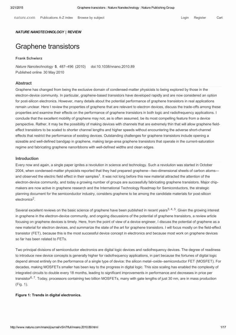
Two principal divisions of semiconductor electronics are digital logic devices and radiofrequency devices. The degree of readinessto introduce new device concepts is generally higher for radiofrequency applications, in part because the fortunes of digital logicdepend almost entirely on the performance of a single type of device: the silicon metal–oxide–semiconductor FET (MOSFET). Fordecades, making MOSFETs smaller has been key to the progress in digital logic. This size scaling has enabled the complexity ofintegrated circuits to double every 18 months, leading to significant improvements in performance and decreases in price pertransistor6, 7. Today, processors containing two billion MOSFETs, many with gate lengths of just 30 nm, are in mass production(Fig. 1).
Figure 1: Trends in digital electronics.
3/21/2015 Graphene transistors : Nature Nanotechnology : Nature Publishing Group
http://www.nature.com/nnano/journal/v5/n7/full/nnano.2010.89.html 2/17
Evolution of MOSFET gate length in productionstage integrated circuits (filled red circles) and International Technology Roadmap forSemiconductors (ITRS) targets (open red circles). As gate lengths have decreased, the number of transistors per processor chip hasincreased (blue stars). Maintaining these trends is a significant challenge for the semiconductor industry, which is why new materials suchas graphene are being investigated.
Because the fabrication of integrated circuits is highly complex, semiconductor fabrication plants are extremely expensive (atpresent costing several billion US dollars). Furthermore, because scaling alone has provided the needed performanceimprovements from one generation of integrated circuits to the next, there has been little motivation for the chipmakers tointroduce devices based on a fundamentally different physics or on a material other than silicon. However, there is a consensus inthe community that MOSFET scaling is approaching its limits and that, in the long run, it will be necessary to introduce newmaterial and device concepts to ensure that performance continues to improve.
The situation is different for radiofrequency electronics. This field was dominated by defence applications until the late 1980s, andalthough it moved into the mainstream in the 1990s owing to advances in wireless communications, the military continued toprovide generous financial support for research into new radiofrequency devices. This, together with the fact that radiofrequencycircuits are much less complex than digital logic chips, has led to makers of radiofrequency chips being more open to new deviceconcepts. An indication of this is the large variety of different transistor types and materials used in radiofrequency electronics:these include highelectronmobility transistors (HEMTs) based on III–V semiconductors such as GaAs and InP, silicon nchannelMOSFETs, and different types of bipolar transistor8, 9.
As I discuss below, graphene is potentially well suited to radiofrequency applications because of its promising carrier transportproperties and its purely twodimensional structure. This, combined with the relative openness of the radiofrequencyelectronicsindustry to new materials, suggests that graphene might make its first appearance in radiofrequency applications rather than inlogic circuits.
FET physics: what really mattersA FET consists of a gate, a channel region connecting source and drain electrodes, and a barrier separating the gate from thechannel (Fig. 2a). The operation of a conventional FET relies on the control of the channel conductivity, and thus the draincurrent, by a voltage, V , applied between the gate and source.
Figure 2: Conventional FETs.
GS

3/21/2015 Graphene transistors : Nature Nanotechnology : Nature Publishing Group
http://www.nature.com/nnano/journal/v5/n7/full/nnano.2010.89.html 3/17
a, Crosssection of an nchannel Si MOSFET. When the voltage applied between the source and gate electrodes exceeds a thresholdvoltage, V , a conducting channel is formed and a drain current, I , flows. The length of the channel is defined by the length of the gateelectrode; the thickness of the gatecontrolled channel region is the depth to which the electronic properties of the semiconductor (pdopedSi in this case) are influenced by the gate. b, FET transfer characteristics showing I (on a logarithmic scale on the left and a linear scaleon the right) versus the gate–source voltage, V . The transistor is considered to be switched on when V is equal to the maximumvoltage supplied to the device, V . The higher the slope in the subthreshold region (V < V ), the better the transistor switchoncharacteristics become. Above threshold, the change in I for a given change in V is called the terminal transconductance, g .
For highspeed applications, FETs should respond quickly to variations in V ; this requires short gates and fast carriers in thechannel. Unfortunately, FETs with short gates frequently suffer from degraded electrostatics and other problems (collectivelyknown as shortchannel effects), such as thresholdvoltage rolloff, draininduced barrier lowering, and impaired draincurrentsaturation7, 10. Scaling theory predicts that a FET with a thin barrier and a thin gatecontrolled region (measured in the verticaldirection in Fig. 2a) will be robust against shortchannel effects down to very short gate lengths (measured in the horizontaldirection in Fig. 2a)11. The possibility of having channels that are just one atomic layer thick is perhaps the most attractive featureof graphene for use in transistors. (Mobility, which is often considered to be graphene's most useful property for applications innanoelectronics, is discussed later.) By comparison, the channels in III–V HEMTs are typically 10–15 nm thick, and althoughsilicononinsulator MOSFETs with channel (that is, silicon body) thicknesses of less than 2 nm have been reported12, rough
Th D
D
GS GS
DD GS Th
D GS mt
GS
3/21/2015 Graphene transistors : Nature Nanotechnology : Nature Publishing Group
http://www.nature.com/nnano/journal/v5/n7/full/nnano.2010.89.html 4/17
interfaces caused their mobility to deteriorate. More importantly, the body of these MOSFETs showed thickness fluctuations thatwill lead to unacceptably large thresholdvoltage variations (and similar problems are expected to occur when the thickness of thechannel in a III–V HEMT is reduced to only a few nanometres). These problems occur at thicknesses that are many times greaterthan the thickness of graphene.
The series resistances between the channel and the source and drain terminals are also important, and their adverse impact onthe FET becomes more pronounced as the gate length decreases13. Thus, device engineers devote considerable effort todeveloping transistor designs in which shortchannel effects are suppressed and series resistances are minimized.
Modern digital logic is based on silicon complementary metal oxide semiconductor (CMOS) technology. CMOS logic gates consistof both n and pchannel MOSFETs that can switch between the onstate (with a large oncurrent, I , and V = ±V , whereV is the maximum voltage supplied to the device) and the offstate (with a small offcurrent, I , and V = 0). In theterminology of digital logic, a gate is not the gate terminal of a transistor but a combination of two or more transistors that canperform a certain logic operation. The value of V at which the FET is just on the verge of switching on is the threshold voltage,V . Figure 2b shows the transfer characteristics of an nchannel FET indicating the onstate and the offstate. Useful measureswith which to assess the switching behaviour are the subthreshold swing, S (relevant to the subthreshold region), and the terminaltransconductance, g (relevant to the abovethreshold region).
In the steady state, a certain number of the MOSFETs in a CMOS logic gate are always switched off so that no current—exceptthe small I —flows through the gate14. The ability of silicon MOSFETs to switch off enables silicon CMOS to offer extremely lowstatic power dissipation (which is the reason why silicon CMOS has bested all competing logic technologies). Thus, any successorto the silicon MOSFET that is to be used in CMOSlike logic must have excellent switching capabilities, as well as an on–off ratio,I /I , of between 104 and 107 (ref. 2). In a conventional FET, this requires semiconducting channels with a sizeable bandgap,preferably 0.4 eV or more. Moreover, n and pchannel FETs with symmetrical threshold voltages, that is, with V = −V ,are needed for proper CMOS operation.
In radiofrequency applications, however, switchoff is not required per se. In smallsignal amplifiers, for example, the transistor isoperated in the onstate and small radiofrequency signals that are to be amplified are superimposed onto the d.c. gate–sourcevoltage. To discuss the radiofrequency performance of FETs, I use the equivalent circuit from Fig. 3a and focus on the cutofffrequency, f , which is the frequency at which the magnitude of the smallsignal current gain rolls off to unity. The cutofffrequency is the most widely used figure of merit for radiofrequency devices and is, in effect, the highest frequency at which a FETis useful in radiofrequency applications.
Figure 3: FET d.c. and smallsignal operation.
on GS DD
DD off GS
GS
Th
mt
off
on off
Th,n Th,p
T

3/21/2015 Graphene transistors : Nature Nanotechnology : Nature Publishing Group
http://www.nature.com/nnano/journal/v5/n7/full/nnano.2010.89.html 5/17

3/21/2015 Graphene transistors : Nature Nanotechnology : Nature Publishing Group
http://www.nature.com/nnano/journal/v5/n7/full/nnano.2010.89.html 6/17
a, Smallsignal equivalent FET circuit. The intrinsic transconductance, g , is related to the internal smallsignal gate–source and drain–source voltages, v and v , whereas the terminal transconductance, g , is related to the applied gate–source and drain–sourcevoltages, V and V (Table 1 and Fig. 2b). b, The drain current, I (blue lines), at different values of V , and the cutoff frequency, f(red line), both versus V for a radiofrequency GaAs highelectronmobility transistor15, 16. The cutoff frequency peaks at V = 1 V andV = 0.15 V. c, The intrinsic transconductance (blue line), the overall gate capacitance, C = C + C (red line), and the drainconductance, g (1/r ; black line), versus V for the same FET.
As can be seen from the expression for f given in Table 1 (Refs 7, 8), the cutoff frequency can be maximized by making theintrinsic transconductance, g , as large as possible and making the drain conductance, g , and all the capacitances andresistances in the equivalent circuit (Fig. 3) as small as possible7, 8. However, the values of all these quantities vary with theapplied d.c. gate–source voltage, V , and the applied d.c. drain–source voltage, V . As shown exemplarily for a typical GaAsHEMT15, 16 (Fig. 3b,c),V has a pronounced effect on the FET performance. For this transistor, f peaks around V = 1 V,that is, deep in the region of draincurrent saturation, where g is near its peak and g has decreased sufficiently. For lowervalues of V , the device operates in the linear regime and the cutoff frequency is low because g is small and g is large.
Table 1: Performance measures for the fieldeffect transistor.
The bottom line for radiofrequency performance is that although shorter gates, faster carriers and lower series resistances all leadto higher cutoff frequencies, saturation of the drain current is essential to reach the maximum possible operating speeds. Thispoint is frequently missed in discussions of transistor speeds. Draincurrent saturation is also necessary to maximize the intrinsicgain, G = g /g , which has become a popular figure of merit for mixedsignal circuits.
Graphene properties relevant to transistorsSinglelayer graphene is a purely twodimensional material. Its lattice consists of regular hexagons with a carbon atom at eachcorner. The bond length between adjacent carbon atoms, L , is 1.42 Å and the lattice constant, a, is 2.46 Å (Fig. 4a). The firstreports on this material appeared decades ago, even before the name graphene had been coined (see, for example, Refs 17, 18,19), but it took the pioneering 2004 paper by the Manchester group1 to spark the present explosion of interest in the material.
Figure 4: Properties of graphene and graphene nanoribbons.
a, Schematic of an armchair (ac) graphene nanoribbon (GNR) of length L and width W . The nanoribbon shown here has N = 9 carbonatoms along its width and thus belongs to the 3p family, where p is an integer. b, Band structure around the K point of (i) largeareagraphene, (ii) graphene nanoribbons, (iii) unbiased bilayer graphene, and (iv) bilayer graphene with an applied perpendicular field. Largeareagraphene and unbiased bilayer graphene do not have a bandgap, which makes them less useful for digital electronics. c, Bandgap versusnanoribbon width from experiments24, 25, 26, 27 and calculations28, 29. By comparison, the bandgap of Si is above 1 eV. zz: zigzag.
At present, the most popular approaches to graphene preparation are mechanical exfoliation1, growth on metals and subsequentgraphene transfer to insulating substrates20, 21, and thermal decomposition of SiC to produce socalled epitaxial graphene on topof SiC wafers22, 23. Exfoliation is still popular for laboratory use but it is not suited to the electronics industry, whereas the othertwo options both have the potential for producing waferscale graphene. After the graphene has been prepared, commonsemiconductor processing techniques (such as lithography, metallization and etching) can be applied to fabricate graphenetransistors.
In this section, I discuss two important aspects of graphene: the presence (or otherwise) of a bandgap, and charge transport(mobility and highfield transport) at room temperature.
m
GSi DSi mt
GS DS D GS T
DS DS
GS G GS GD
ds ds DS
T
m ds
GS DS
DS T DS
m ds
DS m ds
int m ds
b
ac ac

3/21/2015 Graphene transistors : Nature Nanotechnology : Nature Publishing Group
http://www.nature.com/nnano/journal/v5/n7/full/nnano.2010.89.html 7/17
Bandgap. Largearea graphene is a semimetal with zero bandgap. Its valence and conduction bands are coneshaped and meetat the K points of the Brillouin zone (Fig. 4b). Because the bandgap is zero, devices with channels made of largearea graphenecannot be switched off and therefore are not suitable for logic applications. However, the band structure of graphene can bemodified, and it is possible to open a bandgap in three ways: by constraining largearea graphene in one dimension to formgraphene nanoribbons, by biasing bilayer graphene and by applying strain to graphene. See Table 2 and Refs 24, 25, 26, 27, 28,29, 30, 31, 32, 33, 34, 35, 36, 37, 38, 39, 40, 41, 42, 43 for more details.
Table 2: Does graphene have a bandgap?
It has been predicted28 that both armchair nanoribbons and zigzag nanoribbons (the two ideal types of nanoribbon; Fig. 4a) havea bandgap that is, to a good approximation, inversely proportional to the width of the nanoribbon. The opening of a bandgap innanoribbons has been verified experimentally for widths down to about 1 nm (Refs 24, 25, 26, 27), and theory and experimentsboth reveal bandgaps in excess of 200 meV for widths below 20 nm (Fig. 4c). However, it should be noted that real nanoribbonshave rough edges and widths that change along their lengths. Even modest edge disorder obliterates any difference in thebandgap between nanoribbons with different edge geometries29, and edge functionalization and doping can also affect thebandgap44.
To open a bandgap useful for conventional fieldeffect devices, very narrow nanoribbons with welldefined edges are needed. Thisrepresents a serious challenge given the semiconductor processing equipment available at the moment. Recently, nanoribbonsthat were uniform in width and had reduced edge roughness were produced by 'unzipping' carbon nanotubes45. However, even aperfect nanoribbon is not perfect for electronics applications. In general, the larger the bandgap that opens in a nanoribbon, themore the valence and conduction bands become parabolic (rather than coneshaped): this decreases the curvature around the Kpoint and increases the effective mass of the charge carriers46, which is likely to decrease the mobility.
Bilayer graphene is also gapless (Fig. 4b), and its valence and conduction bands have a parabolic shape near the K point. If anelectric field is applied perpendicular to the bilayer, a bandgap opens and the bands near the K point take on the socalledMexicanhat shape. This opening was predicted by theory30, 31 and has been verified in experiments32, 33. Theoreticalinvestigations have also shown that the size of the bandgap depends on the strength of the perpendicular field and can reachvalues of 200–250 meV for high fields ((1–3) × 107 V cm−1; Refs 30,31).
The bandgap of largearea singlelayer epitaxial graphene is at present the subject of controversy34. Although some resultssuggest a zero bandgap37, 38, others report a bandgap of around 0.25 eV (Refs 35, 36). The transfer characteristics of epitaxialgraphene MOSFETs show no switchoff, which suggests a zero bandgap. However, a bandgap is consistently observed forepitaxial bilayer graphene38, 39.
Finally, strain has been discussed as a means of opening a bandgap in largearea graphene, and the effect of uniaxial strain onthe band structure has been simulated40, 41. At present it seems that if it is possible at all, opening a gap in this way will require aglobal uniaxial strain exceeding 20%, which will be difficult to achieve in practice. Moreover, little is known about the ways in whichother types of strain, such as biaxial strain and local strain, influence the band structure of graphene.
Thus, although there are a number of techniques for opening a bandgap in graphene, they are all at the moment some way frombeing suitable for use in realworld applications.
Mobility. The most frequently stated advantage of graphene is its high carrier mobility at room temperature. Mobilities of 10,000–15,000 cm2 V−1 s−1 are routinely measured for exfoliated graphene on SiO covered silicon wafers1, 47, and upper limits ofbetween 40,000 and 70,000 cm2 V−1 s−1 have been suggested47, 48. Moreover, in the absence of charged impurities and ripples,mobilities of 200,000 cm2 V−1 s−1 have been predicted49, and a mobility of 106 cm2 V−1 s−1 was recently reported for suspendedgraphene50. For largearea graphene grown on nickel and transferred to a substrate, mobilities greater than 3,700 cm2 V−1 s−1
have been measured20.
Finally, for epitaxial graphene on silicon carbide, the mobility depends on whether the graphene is grown on the silicon face or thecarbon face of SiC. Although graphene grown on the carbon face has higher mobility (values of ~5,000 cm2 V−1 s−1 have beenreported23, compared with ~1,000 cm2 V−1 s−1 for graphene grown on the silicon face23, 51), it is easier to grow singlelayer andbilayer graphene on the silicon face, which makes the silicon face of SiC more suited for electronic applications.
2

3/21/2015 Graphene transistors : Nature Nanotechnology : Nature Publishing Group
http://www.nature.com/nnano/journal/v5/n7/full/nnano.2010.89.html 8/17
In early graphene MOS structures, the mobility was affected by the use of a topgate dielectric52, 53. However, the recentdemonstration of mobilities of around 23,000 cm2 V−1 s−1 in topgated graphene MOS channels54 and the observation of similarmobilities before and after topgate formation55 show that highmobility graphene MOS channels can be made with a properchoice of the gate dielectric and optimization of the deposition process.
These mobility numbers are impressive, but they require closer inspection. The high mobilities mentioned above relate to largearea graphene, which is gapless. A general trend for conventional semiconductors is that the electron mobility decreases as thebandgap increases, and a similar trend has been predicted for carbon nanotubes (CNTs)56, 57 and graphene nanoribbons58, 59,60, 61 (Fig. 5a). This means that the mobility in nanoribbons with a bandgap similar to that of silicon (1.1 eV) is expected to belower than in bulk silicon and no higher than the mobility in the silicon channel of a conventional MOS device58. The mobilitiesmeasured in experiments—less than 200 cm2 V−1 s−1 for nanoribbons 1–10 nm wide26, 62 and 1,500 cm2 V−1 s−1 for ananoribbon 14 nm wide45 (which is the highest mobility so far measured for a nanoribbon)—support the theoretical results (Fig.5b). Therefore, although the high mobilities offered by graphene can increase the speed of devices, they come at the expense ofmaking it difficult to switch devices off, thus removing one of the main advantages of the CMOS configuration—its low static powerconsumption.
Figure 5: Carrier transport in graphene.
a, Electron mobility versus bandgap in low electric fields for different materials, as indicated (from left to right, III–V compounds are InSb,InAs, In Ga As, InP, GaAs, In Ga P, and GaN). The mobility data relates to undoped material except for the Si MOS data. Alsoshown are mobility data for carbon nanotubes (CNTs; simulation56, 57), graphene nanoribbons (simulation58, 59) and graphene (experimentand simulation47, 48, 49, 50). b, Carrier mobility versus nanoribbon width at low electric fields from simulations60, 61 and experiments (open62
and full45 stars). Data for largearea graphene are also shown1, 47, 48. c, Electron drift velocity versus electric field for commonsemiconductors (Si, GaAs, In Ga As), a carbon nanotube (simulation57) and largearea graphene (simulation63, 64).
Highfield transport. In the days when FETs had gates several micrometres long, the mobility was the appropriate measure ofthe speed of carrier transport. Strictly speaking, however, the mobility describes carrier transport in low electric fields; the shortgate lengths in modern FETs result in high fields in a sizeable portion of the channel, reducing the relevance of mobility to deviceperformance. To illustrate this, let us consider a FET with a gate 100 nm long and a drain–source voltage of 1 V. If we assume avoltage drop of 0.3 V across the series resistances, the average field in the channel is 70 kV cm−1. At such high fields, the steadystate carrier velocity saturates, and this saturation velocity becomes another important measure of carrier transport. Figure 5cshows plots of the electron velocity versus the electric field for conventional semiconductors, and simulated plots for largeareagraphene63, 64 and a carbon nanotube57. For graphene and the nanotube, maximum carrier velocities of around 4 × 107 cm s−1
are predicted, in comparison with 2 × 107 cm s−1 for GaAs and 107 cm s−1 for silicon. Moreover, at high fields the velocity ingraphene and the nanotube does not drop as drastically as in the III–V semiconductors. Unfortunately, there is at present noexperimental data available on highfield transport in graphene nanoribbons and in largearea graphene. However, othermeasurements65 suggest highfield carrier velocities of several 107 cm s−1 in graphene. Thus, regarding highfield transport,graphene and nanotubes seem to have a slight advantage over conventional semiconductors.
Finally, it is worth noting that reported mobilities for graphene devices need to be interpreted carefully because there are severaldefinitions for the MOSFET channel mobility and they are difficult to compare66. Furthermore, the techniques used to measuremobility are only vaguely described in some papers. Most frequently, the fieldeffect mobility, μ , is measured (Table 1).However, the effect of the source and drain series resistances must be eliminated from the measured characteristics to determinethis quantity, and it is not always clear that this has been done.
An additional complication lies in the interpretation of data from topgated graphene MOSFETs, which involves arriving at a valuefor the gate capacitance, C . Frequently C is approximated by the oxide capacitance per unit area, as C = ε /t , where ε
0.53 0.47 0.49 0.51
0.53 0.47
FE
G G ox ox ox ox

3/21/2015 Graphene transistors : Nature Nanotechnology : Nature Publishing Group
http://www.nature.com/nnano/journal/v5/n7/full/nnano.2010.89.html 9/17
is the dielectric constant of the topgate dielectric and t is the thickness of this dielectric. However, when t is small, thequantum capacitance, C , must be taken into account67, 68 because it is connected in series with C , making the overall gatecapacitance C = C C /(C + C ). The overall gate capacitance can be significantly smaller than C , particularly close to theDirac point (the point of minimum drain current), so neglecting the effect of C will lead to an underestimate of the fieldeffectmobility.
State of the art of graphene transistorsA graphene MOS device was among the breakthrough results reported by the Manchester group in 2004 (ref. 1). A 300nm SiOlayer underneath the graphene served as a backgate dielectric and a doped silicon substrate acted as the backgate (Fig. 6a).Such backgate devices have been very useful for proofofconcept purposes, but they suffer from unacceptably large parasiticcapacitances and cannot be integrated with other components. Therefore, practical graphene transistors need a topgate. Thefirst graphene MOSFET with a topgate was reported in 2007 (ref. 52), representing an important milestone, and progress hasbeen very rapid since then (Fig. 6b). Although research into graphene is still in its infancy, graphene MOSFETs can compete withdevices that have benefited from decades of research and investment.
Figure 6: Structure and evolution of graphene MOSFETs.
a, Schematics of different graphene MOSFET types: backgated MOSFET (left); topgated MOSFET with a channel of exfoliated grapheneor of graphene grown on metal and transferred to a SiO covered Si wafer (middle); topgated MOSFET with an epitaxialgraphene channel(right). The channel shown in red can consist of either largearea graphene or graphene nanoribbons. b, Progress in graphene MOSFETdevelopment1, 52, 69, 73 compared with the evolution of nanotube FETs78, 98, 99, 100.
Topgated graphene MOSFETs have been made with exfoliated graphene52, 53, 54, 55, 69, 70, graphene grown on metals such asnickel and copper71, 72, and epitaxial graphene23, 73, 74; SiO , Al O , and HfO have been used for the topgate dielectric. Thechannels of these topgated graphene transistors have been made using largearea graphene, which does not have a bandgap,so they have not been able to switch off.
Largeareagraphene transistors have a unique current–voltage transfer characteristic (Fig. 7a). The carrier density and the typeof carrier (electrons or holes) in the channel are governed by the potential differences between the channel and the gates (topgate and/or backgate). Large positive gate voltages promote an electron accumulation in the channel (ntype channel), and largenegative gate voltages lead to a ptype channel. This behaviour gives rise to the two branches of the transfer characteristicsseparated by the Dirac point (Fig. 7a). The position of the Dirac point depends on several factors: the difference between the workfunctions of the gate and the graphene, the type and density of the charges at the interfaces at the top and bottom of the channel(Fig. 6), and any doping of the graphene. The on–off ratios reported for MOSFET devices with largeareagraphene channels arein the range 2–20.
Figure 7: Directcurrent behaviour of graphene MOSFETs with a largeareagraphene channel.
ox ox
q ox
G ox q ox q ox
q
2
2
2 2 3 2
3/21/2015 Graphene transistors : Nature Nanotechnology : Nature Publishing Group
http://www.nature.com/nnano/journal/v5/n7/full/nnano.2010.89.html 10/17
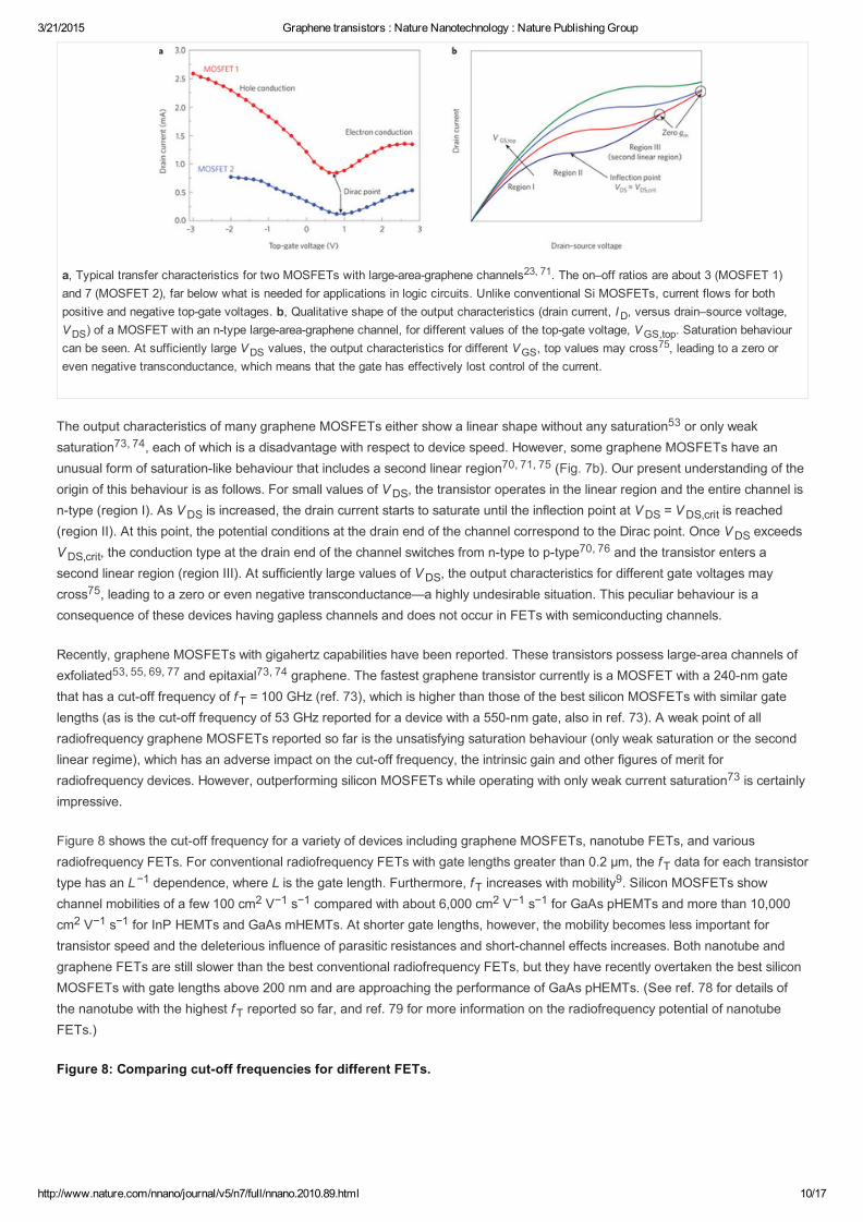
a, Typical transfer characteristics for two MOSFETs with largeareagraphene channels23, 71. The on–off ratios are about 3 (MOSFET 1)and 7 (MOSFET 2), far below what is needed for applications in logic circuits. Unlike conventional Si MOSFETs, current flows for bothpositive and negative topgate voltages. b, Qualitative shape of the output characteristics (drain current, I , versus drain–source voltage,V ) of a MOSFET with an ntype largeareagraphene channel, for different values of the topgate voltage, V . Saturation behaviourcan be seen. At sufficiently large V values, the output characteristics for different V , top values may cross75, leading to a zero oreven negative transconductance, which means that the gate has effectively lost control of the current.
The output characteristics of many graphene MOSFETs either show a linear shape without any saturation53 or only weaksaturation73, 74, each of which is a disadvantage with respect to device speed. However, some graphene MOSFETs have anunusual form of saturationlike behaviour that includes a second linear region70, 71, 75 (Fig. 7b). Our present understanding of theorigin of this behaviour is as follows. For small values of V , the transistor operates in the linear region and the entire channel isntype (region I). As V is increased, the drain current starts to saturate until the inflection point at V = V is reached(region II). At this point, the potential conditions at the drain end of the channel correspond to the Dirac point. Once V exceedsV , the conduction type at the drain end of the channel switches from ntype to ptype70, 76 and the transistor enters asecond linear region (region III). At sufficiently large values of V , the output characteristics for different gate voltages maycross75, leading to a zero or even negative transconductance—a highly undesirable situation. This peculiar behaviour is aconsequence of these devices having gapless channels and does not occur in FETs with semiconducting channels.
Recently, graphene MOSFETs with gigahertz capabilities have been reported. These transistors possess largearea channels ofexfoliated53, 55, 69, 77 and epitaxial73, 74 graphene. The fastest graphene transistor currently is a MOSFET with a 240nm gatethat has a cutoff frequency of f = 100 GHz (ref. 73), which is higher than those of the best silicon MOSFETs with similar gatelengths (as is the cutoff frequency of 53 GHz reported for a device with a 550nm gate, also in ref. 73). A weak point of allradiofrequency graphene MOSFETs reported so far is the unsatisfying saturation behaviour (only weak saturation or the secondlinear regime), which has an adverse impact on the cutoff frequency, the intrinsic gain and other figures of merit forradiofrequency devices. However, outperforming silicon MOSFETs while operating with only weak current saturation73 is certainlyimpressive.
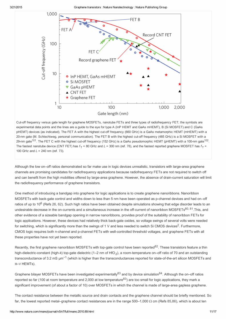
Figure 8 shows the cutoff frequency for a variety of devices including graphene MOSFETs, nanotube FETs, and variousradiofrequency FETs. For conventional radiofrequency FETs with gate lengths greater than 0.2 μm, the f data for each transistortype has an L−1 dependence, where L is the gate length. Furthermore, f increases with mobility9. Silicon MOSFETs showchannel mobilities of a few 100 cm2 V−1 s−1 compared with about 6,000 cm2 V−1 s−1 for GaAs pHEMTs and more than 10,000cm2 V−1 s−1 for InP HEMTs and GaAs mHEMTs. At shorter gate lengths, however, the mobility becomes less important fortransistor speed and the deleterious influence of parasitic resistances and shortchannel effects increases. Both nanotube andgraphene FETs are still slower than the best conventional radiofrequency FETs, but they have recently overtaken the best siliconMOSFETs with gate lengths above 200 nm and are approaching the performance of GaAs pHEMTs. (See ref. 78 for details ofthe nanotube with the highest f reported so far, and ref. 79 for more information on the radiofrequency potential of nanotubeFETs.)
Figure 8: Comparing cutoff frequencies for different FETs.
D
DS GS,top
DS GS
DS
DS DS DS,crit
DS
DS,crit
DS
T
T
T
T
3/21/2015 Graphene transistors : Nature Nanotechnology : Nature Publishing Group
http://www.nature.com/nnano/journal/v5/n7/full/nnano.2010.89.html 11/17
Cutoff frequency versus gate length for graphene MOSFETs, nanotube FETs and three types of radiofrequency FET; the symbols areexperimental data points and the lines are a guide to the eye for type A (InP HEMT and GaAs mHEMT), B (Si MOSFET) and C (GaAspHEMT) devices (as indicated). The FET A with the highest cutoff frequency (660 GHz) is a GaAs metamorphic HEMT (mHEMT) with a20nm gate (M. Schlechtweg, personal communication). The FET B with the highest cutoff frequency (485 GHz) is a Si MOSFET with a29nm gate101. The FET C with the highest cutoff frequency (152 GHz) is a GaAs pseudomorphic HEMT (pHEMT) with a 100nm gate102.The fastest nanotube device (CNT FET) has f = 80 GHz and L = 300 nm (ref. 78), and the fastest reported graphene MOSFET has f =100 GHz and L = 240 nm (ref. 73).
Although the low on–off ratios demonstrated so far make use in logic devices unrealistic, transistors with largearea graphenechannels are promising candidates for radiofrequency applications because radiofrequency FETs are not required to switch offand can benefit from the high mobilities offered by largearea graphene. However, the absence of draincurrent saturation will limitthe radiofrequency performance of graphene transistors.
One method of introducing a bandgap into graphene for logic applications is to create graphene nanoribbons. NanoribbonMOSFETs with backgate control and widths down to less than 5 nm have been operated as pchannel devices and had on–offratios of up to 106 (Refs 26, 62). Such high ratios have been obtained despite simulations showing that edge disorder leads to anundesirable decrease in the oncurrents and a simultaneous increase in the offcurrent of nanoribbon MOSFETs80, 81.This, andother evidence of a sizeable bandgap opening in narrow nanoribbons, provides proof of the suitability of nanoribbon FETs forlogic applications. However, these devices had relatively thick backgate oxides, so voltage swings of several volts were neededfor switching, which is significantly more than the swings of 1 V and less needed to switch Si CMOS devices2. Furthermore,CMOS logic requires both nchannel and pchannel FETs with wellcontrolled threshold voltages, and graphene FETs with allthese properties have not yet been reported.
Recently, the first graphene nanoribbon MOSFETs with topgate control have been reported82. These transistors feature a thinhighdielectricconstant (highk) topgate dielectric (1–2 nm of HfO ), a roomtemperature on–off ratio of 70 and an outstandingtransconductance of 3.2 mS μm−1 (which is higher than the transconductances reported for stateoftheart silicon MOSFETs andIII–V HEMTs).
Graphene bilayer MOSFETs have been investigated experimentally83 and by device simulation84. Although the on–off ratiosreported so far (100 at room temperature and 2,000 at low temperature83) are too small for logic applications, they mark asignificant improvement (of about a factor of 10) over MOSFETs in which the channel is made of largearea gapless graphene.
The contact resistance between the metallic source and drain contacts and the graphene channel should be briefly mentioned. Sofar, the lowest reported metal–graphene contact resistances are in the range 500–1,000 Ω cm (Refs 85,86), which is about ten
T T
2
3/21/2015 Graphene transistors : Nature Nanotechnology : Nature Publishing Group
http://www.nature.com/nnano/journal/v5/n7/full/nnano.2010.89.html 12/17
times the contact resistance of silicon MOSFETs and III–V HEMTs8, 13. Remarkably, in spite of the importance of the contacts(particularly for shortchannel devices), only a few studies dealing with metal–graphene contacts have been published85, 86, 87
and more work is needed to understand the contact properties.
I now return to the twodimensional nature of graphene. According to scaling theory, as noted previously, a thin channel regionallows shortchannel effects to be suppressed and thus makes it feasible to scale MOSFETs to very short gate lengths. The twodimensional nature of graphene means it offers us the thinnest possible channel, so graphene MOSFETs should be morescalable than their competitors. It should be noted, however, that scaling theory is valid only for transistors with a semiconductingchannel and does not apply to graphene MOSFETs with gapless channels. Thus, the scaling theory does describe nanoribbonMOSFETs, which have a bandgap but which have significantly lower mobilities than largearea graphene, as discussed. Giventhat the high published values of mobility relate to gapless largearea graphene, the most attractive characteristic of graphene foruse in MOSFETs, in particular those required to switch off, may be its ability to scale to shorter channels and higher speeds,rather than its mobility.
Further options for graphene devicesIt has become clear that graphene devices based on the conventional MOSFET principle suffer from some fundamentalproblems. This has motivated researchers to explore new graphene device concepts, such as tunnel FETs and bilayerpseudospin FETs. In a tunnel FET, the bandtoband tunnelling across the source–channel junction can be controlled using thegate–source voltage. The big advantage of tunnel FETs is that their subthreshold swings are not limited to 60 mV per decade, asin conventional MOSFETs7, 10, which should lead to steeper subthreshold characteristics and better switchoff. The tunnelFETapproach has already been explored in silicon and carbonnanotube MOSFETs88, 89. Tunnel FETs based on nanoribbons andbilayer graphene have been investigated in simulations84, 90, 91 but have not been demonstrated experimentally. In particular, thebilayer graphene tunnel FET is now considered to be a promising device for a number of reasons: narrow nanoribbons are notneeded, so edge disorder will not be a problem and patterning will be relatively easy; the small bandgap opened by a vertical fieldapplied across the two layers is sufficient to suppress bandtoband tunnelling in the offstate and thus enables effective switchoff;and the possibility of subthreshold swings below 60 mV per decade should make high on–off ratios possible84.
The bilayer pseudospin FET consists of a vertical stack of two graphene layers separated by a thin dielectric92. Under certain biasconditions the tunnelling resistance between the two graphene layers becomes so small that the layers are effectively shorted,causing the FET to pass a high current, whereas under other conditions the tunnelling resistance is very large, shutting thecurrent off. The bilayer pseudospin FET might therefore be able to deliver fast and ultralowpower logic operation.
Although graphene tunnel FETs and bilayer pseudospin FETs are both still at an embryonic stage, they have already gainedconsiderable attention in the electrondevice community and have been included in the chapter on emerging research devices inthe latest edition of the ITRS2. It might also be possible to make interconnects from graphene, which would open the possibility ofallgraphene integrated circuits in which both the active devices and the wiring were made of graphene22. It has been shown thatgraphene interconnects compete well with copper interconnects93, 94; indeed, graphene can support current densities greaterthan 108 A cm−2 (which is 100 times higher than those supported by copper and is comparable with those supported bynanotubes)95 and has a thermal conductivity of around 30–50 W cm−1 K−1 (in comparison with 4 W cm−1 K−1 for copper)96.
OutlookSince 2007, we have witnessed huge progress in the development of graphene transistors. Most impressive were thedemonstrations of a graphene MOSFET with a cutoff frequency of 100 GHz (ref. 73), the excellent switching behaviour ofnanoribbon MOSFETs26, 62, and channel mobilities exceeding 20,000 cm2 V−1 s−1 in topgated graphene MOSFETs54.However, this progress has been accompanied by the appearance of a number of problems. MOSFETs with largeareagraphenechannels cannot be switched off, making them unsuitable for logic applications, and their peculiar saturation behaviour limits theirradiofrequency performance. Nanoribbon graphene, which does have a bandgap and results in transistors that can be switchedoff, has serious fabrication issues because of the small widths required and the presence of edge disorder.
The primary challenges facing the community at present, therefore, are to create in a controlled and practical fashion a bandgapin graphene, which would allow logic transistors to switch off and radiofrequency transistors to avoid the second linear regime (Fig.7b), and to develop other means of improving transistor saturation characteristics by, for example, developing contacts that blockone kind of carrier without degrading the transistor's speed. The community may also benefit from recognizing that the motivationto use graphene in transistors in the first place stems less from ultrahigh mobilities than from graphene's ability to scale to short

3/21/2015 Graphene transistors : Nature Nanotechnology : Nature Publishing Group
http://www.nature.com/nnano/journal/v5/n7/full/nnano.2010.89.html 13/17
gate lengths and high speeds by virtue of its thinness.
This discussion of the problems of graphene MOSFETs should not lead to the conclusion that graphene is not a promisingmaterial for transistors. Rather, I have chosen a more critical view to avoid a situation that has been seen in the past, in which anew device or material concept has been prematurely declared capable of replacing the status quo. Also, I agree with DavidFerry, a veteran of semiconductor device research, when he says that97 “many such saviours have come and gone, yet thereliable silicon CMOS continues to be scaled and to reach even higher performance levels”.
I conclude by noting that the first topgated graphene transistors were reported only three years ago. Given this short history, andgiven that all other possible successors to conventional mainstream transistors also face serious problems, we cannot help but beimpressed with the rapid development of graphene. Concepts that have been investigated for many years, such as spintransistors or molecular devices, seem to be farther from real application than does graphene, and it is not clear if they will everreach the production stage. At the moment, it is impossible to say which, if any, of the alternative device concepts beingconsidered will replace conventional transistors. However, the latest ITRS roadmap strongly recommends intensified research intographene and even contains a research and development schedule for carbonbased nanoelectronics2. The race is still open andthe prospects for graphene devices are at least as promising as those for alternative concepts.
References1. Novoselov, K. S. et al. Electric field effect in atomically thin carbon films. Science 306, 666–669 (2004).
2. The International Technology Roadmap for Semiconductors http://www.itrs.net/Links/2009ITRS/Home2009.htm(Semiconductor Industry Association, 2009).
3. Geim, A. K. & Novoselov, K. S. The rise of graphene. Nature Mater. 6, 183–191 (2007).
4. Geim, A. K. Graphene: status & prospects. Science 324, 1530–1534 (2009).
5. Castro Neto, A. H. et al. The electronic properties of graphene. Rev. Mod. Phys. 81, 109–162 (2009).
6. Moore, G. E. in Tech. Dig. ISSCC 20–23 (IEEE, 2003).
7. Schwierz, F., Wong, H. & Liou, J. J. Nanometer CMOS (Pan Stanford, 2010).
8. Schwierz, F. & Liou, J. J. Modern Microwave Transistors – Theory, Design, and Performance (Wiley, 2003).
9. Schwierz, F. & Liou, J. J. RF transistors: recent developments and roadmap toward terahertz applications. SolidStateElectron. 51, 1079–1091 (2007).
10. Taur, Y. & Ning, T. H. Fundamentals of Modern VLSI Devices(Cambridge Univ. Press, 1998).
11. Frank, D. J., Taur, Y. & Wong, HS. P. Generalized scale length for twodimensional effects in MOSFETs. IEEE ElectronDev. Lett. 19, 385–387 (1998).
12. Aberg, I. & Hoyt, J. L. Hole transport in ultrathinbody MOSFETs in strainedSi directly on insulator with strainedSithickness less than 5 nm. IEEE Electron Dev. Lett. 26, 661–663 (2005).
13. Thompson, S. E. et al. In search of “forever”, continued transistor scaling one new material at a time. IEEE Trans.Semicond. Manuf. 18, 26–36 (2005).
14. Uyemura, J. P. CMOS Logic Circuit Design (Kluwer Academic, 1999).
15. Hughes, B. & Tasker, P. J. Bias dependence of the MODFET intrinsic model elements values at microwave frequencies.IEEE Trans. Electron. Dev. 36, 2267–2273 (1989).
16. Nguyen, L. D. et al. in Tech. Dig. IEDM 176–179 (IEEE, 1988).
17. Boehm, H. P., Clauss, A., Hofmann, U. & Fischer, G. O. Dünnste KohlenstoffFolien. Z. Naturforsch. B 17, 150–153 (1962).
18. May, J. W. Platinum surface LEED rings. Surf. Sci. 17, 267–270 (1969).
19. van Bommel, A. J., Crombeen, J. E. & van Tooren, A. LEED and Auger electron observations of the SiC (0001) surface.Surf. Sci. 48, 463–472 (1975).
20. Kim, KS. et al. Largescale pattern growth of graphene films for stretchable transparent electrodes. Nature 457, 706–710(2009).

3/21/2015 Graphene transistors : Nature Nanotechnology : Nature Publishing Group
http://www.nature.com/nnano/journal/v5/n7/full/nnano.2010.89.html 14/17
21. Reina, A. et al. Large area, fewlayer graphene films on arbitrary substrates by chemical vapor deposition. Nano Lett. 9,30–35 (2009).
22. Berger, C. et al. Electronic confinement and coherence in patterned epitaxial graphene. Science 312, 1191–1196 (2006).
23. Kedzierski, J. et al. Epitaxial graphene transistors on SiC substrates. IEEE Trans. Electron. Dev. 55, 2078–2085 (2008).
24. Han, M. et al. Energy bandgap engineering of graphene nanoribbons. Phys. Rev. Lett. 98, 206805 (2007).
25. Kim, P. et al. in Tech. Dig. IEDM 241–244 (IEEE, 2009).
26. Li, X., Wang, X., Zhang, L., Lee, S. & Dai, H. Chemically derived, ultrasmooth graphene nanoribbon semiconductors.Science 319, 1229–1232 (2008).
27. Chen, Z., Lin, YM., Rooks, M. J. & Avouris, Ph. Graphene nanoribbon electronics. Physica E 40, 228–232 (2007).
28. Yang, L. et al. Quasiparticle energies and band gaps in graphene nanoribbons. Phys. Rev. Lett. 99, 186801 (2007).
29. Evaldsson, M., Zozoulenko, I. V., Xu, H. & Heinzel, T. Edgedisorderinduced Anderson localization and conduction gap ingraphene nanoribbons. Phys. Rev. B 78, 161407 (2008).
30. Castro, E. V. et al. Biased bilayer graphene: semiconductor with a gap tunable by the electric field effect. Phys. Rev. Lett.99, 216802 (2007).
31. Gava, P., Lazzeri, M., Saitta, A. M. & Mauri, F. Ab initio study of gap opening and screening effects in gated bilayergraphene. Phys. Rev. B 79, 165431 (2009).
32. Ohta, T., Bostwick, A., Seyller, Th., Horn, K. & Rotenberg, E. Controlling the electronic structure of bilayer graphene.Science 313, 951–954 (2006).
33. Zhang, Y. et al. Direct observation of a widely tunable bandgap in bilayer graphene. Nature 459, 820–823 (2009).
34. Rotenberg, E. et al. and Zhou, S. Y. et al. Origin of the energy bandgap in epitaxial graphene. Nature Mater. 7, 258–260(2008).
35. Zhou, S. Y. et al. Substrateinduced bandgap opening in epitaxial graphene. Nature Mater. 6, 770–775 (2007).
36. Kim, S., Ihm, J., Choi, H. J. & Son, YW. Origin of anomalous electronic structures of epitaxial graphene on silicon carbide.Phys. Rev. Lett. 100, 176802 (2008).
37. Bostwick, A., Ohta, T., Seyller, Th., Horn, K. & Rotenberg, E. Quasiparticle dynamics in graphene. Nature Phys. 3, 36–40(2007).
38. Peng, X. & Ahuja, R. Symmetry breaking induced bandgap in epitaxial graphene layers on Si. Nano Lett. 8, 4464–4468(2008).
39. Sano, E. & Otsuji, T. Theoretical evaluation of channel structure in graphene fieldeffect transistors. Jpn. J. Appl. Phys. 48,041202 (2009).
40. Pereira, V. M., Castro Neto, A. H. & Peres, N. M. R. Tightbinding approach to uniaxial strain in graphene. Phys. Rev. B 80,045401 (2009).
41. Ni, Z. H. et al. Uniaxial strain on graphene: Raman spectroscopy study and bandgap opening. ACS Nano 2, 2301–2305(2008); erratum 3, 483 (2009).
42. Sols, F., Guinea, F. & Castro Neto, A. H. Coulomb blockade in graphene nanoribbons. Phys. Rev. Lett. 99, 166803 (2007).
43. Han, M. Y., Brant, J. C. & Kim, P. Electron transport in disordered graphene nanoribbons. Phys. Rev. Lett. 104, 056801(2010).
44. CervantesSodi, F., Csanyi, G., Picanec, S. & Ferrari, A. C. Edgefunctionalized and substitutionally doped graphenenanoribbons: electronic and spin properties. Phys. Rev. B 77, 165427 (2008).
45. Jiao, J., Wang, X., Diankov, G., Wang, H. & Dai, H. Facile synthesis of highquality graphene nanoribbons. NatureNanotech. 5, 321–325 (2010).
46. Raza, H. & Kan, E. C. Armchair graphene nanoribbons: electronic structure and electricfield modulation. Phys. Rev. B 77,245434 (2008).

3/21/2015 Graphene transistors : Nature Nanotechnology : Nature Publishing Group
http://www.nature.com/nnano/journal/v5/n7/full/nnano.2010.89.html 15/17
47. Chen, JH., Jang, C., Xiao, S., Ishigami, M. & Fuhrer, M. S. Intrinsic and extrinsic performance limits of graphene deviceson SiO . Nature Nanotech. 3, 206–209 (2008).
48. Chen, F., Xia, J., Ferry, D. K. & Tao, N. Dielectric screening enhanced performance in graphene FET. Nano Lett. 9,2571–2574 (2009).
49. Morozov, V. S. et al. Giant intrinsic carrier mobilities in graphene and its bilayer. Phys. Rev. Lett. 100, 016602 (2008).
50. Geim, A. Graphene update. Bull. Am. Phys. Soc. 55, abstr. J21.0004, http://meetings.aps.org/link/BAPS.2010.MAR.J21.4(2010).
51. Emtsev, K. V. et al. Towards wafersize graphene layers by atmospheric pressure graphitization of silicon carbide. NatureMater. 8, 203–207 (2009).
52. Lemme, M. C., Echtermeyer, T. J., Baus, M. & Kurz, H. A graphene fieldeffect device. IEEE Electron Dev. Lett. 28,282–284 (2007).
53. Lin, YM. et al. Operation of graphene transistors at gigahertz frequencies. Nano Lett. 9, 422–426 (2009).
54. Liao, L. et al. Highκ oxide nanoribbons as gate dielectrics for high mobility topgated graphene transistors. Proc. Natl Acad.Sci. USA 107, 6711–6715 (2010).
55. Farmer, D. B. et al. Utilization of a buffered dielectric to achieve high fieldeffect carrier mobility in graphene transistors.Nano Lett. 9, 4474–4478 (2009).
56. Zhou, X., Park, JY., Huang, S., Liu, J. & McEuen, P. L. Band structure, phonon scattering, and performance limit of singlewalled carbon nanotube transistors. Phys. Rev. Lett. 95, 146805 (2005).
57. Perebeinos, V., Tersoff, J. & Avouris, Ph. Electronphonon interaction and transport in semiconducting carbon nanotubes.Phys. Rev. Lett. 94, 0786802 (2005).
58. Obradovic, B. et al. Analysis of graphene nanoribbons as a channel material for fieldeffect transistors. Appl. Phys. Lett. 88,142102 (2006).
59. Fang, T., Konar, A., Xing, H. & Jena, D. Mobility in semiconducting nanoribbons: phonon, impurity, and edge roughnessscattering. Phys. Rev. B 78, 205403 (2008).
60. Bresciani, M., Palestri, P., Esseni, D. & Selmi, L. in Proc. ESSDERC '09 480–483 (IEEE, 2009).
61. Betti, A., Fiori, G., Iannaccone, G. & Mao, Y. in Tech. Dig. IEDM 2009 897–900 (IEEE, 2009).
62. Wang, X. et al. Roomtemperature allsemiconducting sub10nm graphene nanoribbon fieldeffect transistors. Phys. Rev.Lett. 100, 206803 (2008).
63. Akturk, A. & Goldsman, N. Electron transport and fullband electronphonon interactions in graphene. J. Appl. Phys. 103,053702 (2008).
64. Shishir, R. S. & Ferry, D. K. Velocity saturation in intrinsic graphene. J. Phys. Condens. Matter 21, 344201 (2009).
65. Barreiro, A., Lazzeri, M., Moser, J., Mauri, F. & Bachtold, A. Transport properties of graphene in the highcurrent limit.Phys. Rev. Lett. 103, 076601 (2009).
66. Schroder, D. K. Semiconductor Material and Device Characterization (Wiley, 1990).
67. Fang, T., Konar, A., Xing, H. & Jena, D. Carrier statistics and quantum capacitance of graphene sheets and nanoribbons.Appl. Phys. Lett. 91, 092109 (2007).
68. Chen, Z. & Appenzeller, J. in Tech. Dig. IEDM 2008, paper 21.1 (IEEE, 2008).
69. Meric, I., Baklitskaya, N., Kim, P. & Shepard, K. L. in Tech. Dig. IEDM 2008, paper 21.2 (IEEE, 2008).
70. Meric, I. et al. Current saturation in zerobandgap, topgated graphene fieldeffect transistors. Nature Nanotech. 3, 654–659(2008).
71. Kedzierski, J. et al. Grapheneoninsulator transistors made using C on Ni chemicalvapor deposition. IEEE Electron Dev.Lett. 30, 745–747 (2009).
72. Li, X. et al. Largearea synthesis of highquality and uniform graphene films on copper foils. Science 324, 1312–1314
2

3/21/2015 Graphene transistors : Nature Nanotechnology : Nature Publishing Group
http://www.nature.com/nnano/journal/v5/n7/full/nnano.2010.89.html 16/17
(2009).
73. Lin, YM. et al. 100GHz transistors from waferscale epitaxial graphene. Science 327, 662 (2010).
74. Moon, J. S. et al. Epitaxialgraphene RF fieldeffect transistors on Siface 6HSiC substrates. IEEE Electron Dev. Lett. 30,650–652 (2009).
75. Tahy, K. et al. in Proc. Dev. Res. Conf. 2009 207–208 (IEEE, 2009).
76. Thiele, S., Schaefer, J. A. & Schwierz, F. Modeling of graphene metal–oxide–semiconductor fieldeffect transistors withgapless largearea graphene channels. J. Appl. Phys. 107, 094505 (2010).
77. Lin, YM. et al. Dualgate graphene FETs with f of 50 GHz. IEEE Electron Dev. Lett. 31, 68–70 (2010).
78. Nougaret, N. et al. 80 GHz fieldeffect transistors produced using high purity semiconducting singlewalled carbonnanotubes. Appl. Phys. Lett. 94, 243505 (2009).
79. Rutherglen, C., Jain, D. & Burke, P. Nanotube electronics for radiofrequency applications. Nature Nanotech. 4, 811–819(2009).
80. Yoon, Y. & Guo, J. Effects of edge roughness in graphene nanoribbon transistors. Appl. Phys. Lett. 91, 073103 (2007).
81. Basu, D., Gilbert, M. J., Register, L. F., Banerjee, S. K. & MacDonald, A. H. Effect of edge roughness on electronictransport in graphene nanoribbon channel metal–oxide–semiconductor fieldeffect transistors. Appl. Phys. Lett. 92, 042114(2008).
82. Liao, L. et al. Topgated graphene nanoribbon transistors with ultrathin highk dielectrics. Nano Lett. 10, 1917–1921 (2010).
83. Xia, F., Farmer, D. B., Lin, YM. & Avouris, Ph. Graphene fieldeffect transistors with high on/off current ratio and largetransport band gap at room temperature. Nano Lett. 10, 715–718 (2010).
84. Iannaccone, G. et al. in Tech. Dig. IEDM 2009 245–248 (IEEE, 2009).
85. Nagashio, K., Nishimura, T., Kita, K. & Toriumi, A. in Tech. Dig. IEDM 2009 565–568 (IEEE, 2009).
86. Russo, S., Cracuin, M. F., Yamamoto, Y., Morpurgo, A. F. & Tarucha, S. Contact resistance in graphenebased devices.Physica E 42, 677–679 (2010).
87. Huard, B., Stander, N., Sulpizio, J. A. & GoldhaberGordon, D. Evidence of the role of contacts on the observed electronhole asymmetry in graphene. Phys. Rev. B 78, 121402 (2008).
88. Boucart, K. & Ionescu, A. M. Doublegate tunnel FET with highκ gate dielectric. IEEE Trans. Electron. Dev. 54, 1725–1733(2007).
89. Appenzeller, J., Lin, YM., Knoch, J. & Avouris, Ph. Bandtoband tunneling in carbon nanotube fieldeffect transistor. Phys.Rev. Lett. 93, 196805 (2004).
90. Luisier, M. & Klimeck, G. in Proc. Dev. Res. Conf. 2009 201–202 (IEEE, 2009).
91. Fiori, G. & Iannaccone, G. Ultralowvoltage bilayer graphene tunnel FET. IEEE Electron Dev. Lett. 30, 1096–1098 (2009).
92. Banerjee, S. K., Register, L. F., Tutuc, E., Reddy, D. & MacDonald, A. H. Bilayer pseudospin fieldeffect transistor(BiSFET): a proposed new logic device. IEEE Electron Dev. Lett. 30, 158–160 (2009).
93. Murali, R., Brenner, K., Yang, Y., Beck, Th. & Meindl, J. D. Resistivity of graphene nanoribbon interconnects. IEEEElectron Dev. Lett. 30, 611–613 (2009).
94. Awano, Y. in Tech. Dig. IEDM 2009 233–236 (IEEE, 2009).
95. Moser, J., Barreiro, A. & Bachtold, A. Currentinduced cleaning of graphene. Appl. Phys. Lett. 91, 163513 (2007).
96. Balandin, A. A. et al. Superior thermal conductivity of singlelayer graphene. Nano Lett. 8, 902–907 (2008).
97. Ferry, D. K., Gilbert, M. J. & Akis, R. Some considerations on nanowires in nanoelectronics. IEEE Trans. Electron. Dev. 55,2820–2826 (2008).
98. Iijima, S. Helical microtubules of graphitic carbon. Nature 354, 56–58 (1991).
99. Tans, S. J., Verschueren, A. R. M. & Dekker, C. Roomtemperature transistor based on a single carbon nanotube. Nature
T

3/21/2015 Graphene transistors : Nature Nanotechnology : Nature Publishing Group
http://www.nature.com/nnano/journal/v5/n7/full/nnano.2010.89.html 17/17
Nature Nanotechnology ISSN 17483387 EISSN 17483395 Banner image © Ward Lopes, Heinrich Jaeger
© 2010 Macmillan Publishers Limited. All Rights Reserved.
partner of AGORA, HINARI, OARE, INASP, ORCID, CrossRef and COUNTER
393, 49–52 (1998).
100. Li, S., Yu, Z., Yen, SF., Tang, W. C. & Burke, P. J. Carbon nanotube transistor operation at 2.6 GHz. Nano Lett. 4,753–756 (2004).
101. Lee, S. et al. in Tech. Dig. IEDM 2007 255–258 (IEEE, 2007).
102. Nguyen, L. D., Tasker, P. J., Radulescu, D. C. & Eastman, L. F. Characterization of ultrahighspeed AlGaAs/InGaAs (onGaAs) MODFETs. IEEE Trans. Electron. Dev. 36, 2243–2248 (1989).
Download references
AcknowledgementsThis work was financially supported by the 2008–2009 Excellence Research Grant of Technische Universität Ilmenau. The authorthanks A. Castro Neto, K. Novoselov and Th. Seyller for discussions. He also thanks St. Thiele for his comments and forgraphene MOSFET simulations, and M. Schlechtweg for providing GaAs metamorphicHEMT data before publication.
Author informationAffiliationsTechnische Universität Ilmenau, Postfach 100565, 98694 Ilmenau, Germany. Frank Schwierz
Competing financial interestsThe author declares no competing financial interests.