gpus/data parallel accelerators dezső sima nov. 2008 © dezső sima 2008 ver. 1.0
TRANSCRIPT

GPUs/Data Parallel Accelerators
Dezső Sima
Nov. 2008
© Dezső Sima 2008Ver. 1.0

2. Basics of the SIMT execution
Content
s
1.Introduction
3. Overview of GPGPUs
4. Overview of data parallel accelerators
5. Microarchitecture and operation
5.1 Nvidia’s GPGPU line
5.2 Intel’s Larrabee
6. References

1. The emergence of GPGPUs

Programming of 3D graphical apps on GPUs
GPUs are programmed traditionally by using 3D graphics API libraries, such as
• the open source OpenGL
• Mirosoft’s Direct3D
(that is part of Microsoft’ s DirectX API and is supported by Microsoft’s Windows OS)
Both API libraries provide – among others - shaders
Shaders:
set of instructions used to achieve rendering
Rendering:
Generating an image from its 3-dimensional description, that includes geometry, viewpoint, texture, lighting and shading information
Graphics APIs act as a layer between the application and the graphics hardware.Programmers write their code by using the same APIs for different GPUs, it is the API’s task to translate this code to instructions understandable to the graphics hardware.
This approach releases the programmer from the need to use device specific instructions.
Note
1. The emergence of GPGPUs (1)

Main types of shaders
Shaders
Geometry shaders Vertex shaders Pixel shaders(Fragment shaders)
Transform each vertex’s 3D-position in the virtual space
to the 2D coordinate, at which it appears on the screen
Calculate the color of the pixels
Can add or removevertices from a mesh
Note
In computer graphics objects are typically represented by triangles,
1. The emergence of GPGPUs (2)

Vertex
Edge Surface
Vertices
• have three spatial coordinates• supplementary information necessary to render the object, such as
• color• texture• reflectance properties• etc.
Triangulated representation of objects
1. The emergence of GPGPUs (3)

Support of shaders in graphics API libraries
Subsequent versions of Graphics API libraries support different underlying shader models (SM) [21].
E.g. DirectX9 (issued in 12/2002) supports SM2 DirectX9.0c (08/2004) SM3 DirectX10 (11/2006) SM4.
1. The emergence of GPGPUs (4)

DirectX version Pixel SM Vertex SM Supporting OS
8.0 (11/2000) 1.0, 1.1 1.0, 1.1 Windows 2000
8.1 (10/2001) 1.2, 1.3, 1.4 1.0, 1.1 Windows XP/ Windows Server 2003
9.0 (12/2002) 2.0 2.0
9.0a (3/2003) 2_A, 2_B 2.x
9.0c (8/2004) 3.0 3.0 Windows XP SP2
10.0 (11/2006) 4.0 4.0 Windows Vista
10.1 (2/2008) 4.1 4.1 Windows Vista SP1/ Windows Server 2008
11 (in development) 5.0 5.0
Table: Pixel/vertex shader models (SM) supported by subsequent versions of DirectXand MS’s OSs [18], [21]
1. The emergence of GPGPUs (5)

Convergence of important features of the vertex and pixel shader models
Subsequent shader models introduce typically, a number of new/enhanced features.
Shader model 2 [19]
• Different precision requirements
Vertex shader: FP32 (coordinates)
Pixel shader: FX24 (3 colors x 8)
• Different instructions
• Different resources (e.g. registers)
Differences between the vertex and pixel shader models in subsequent shader models concerning precision requirements, instruction sets and programming resources.
Shader model 3 [19]
• Unified precision requirements for both shaders (FP32) with the option to specify partial precision (FP16 or FP24) by adding a modifier to the shader code
• Different instructions
• Different resources (e.g. registers)
1. The emergence of GPGPUs (6)

Shader model 4 (introduced with DirectX10) [20]
• Unified precision requirements for both shaders (FP32) with the possibility to use new data formats.
• Unified instruction set
• Unified resources (e.g. temporary and constant registers)
Shader architectures of GPUs prior to SM4
GPUs prior to SM4 (DirectX 10):
have separate vertex and pixel units with different features. Drawback of having separate units for vertex and pixel shading
Inefficiency of the hardware implementation(Vertex shaders and pixel shaders often have complementary load patterns [21]).
1. The emergence of GPGPUs (7)
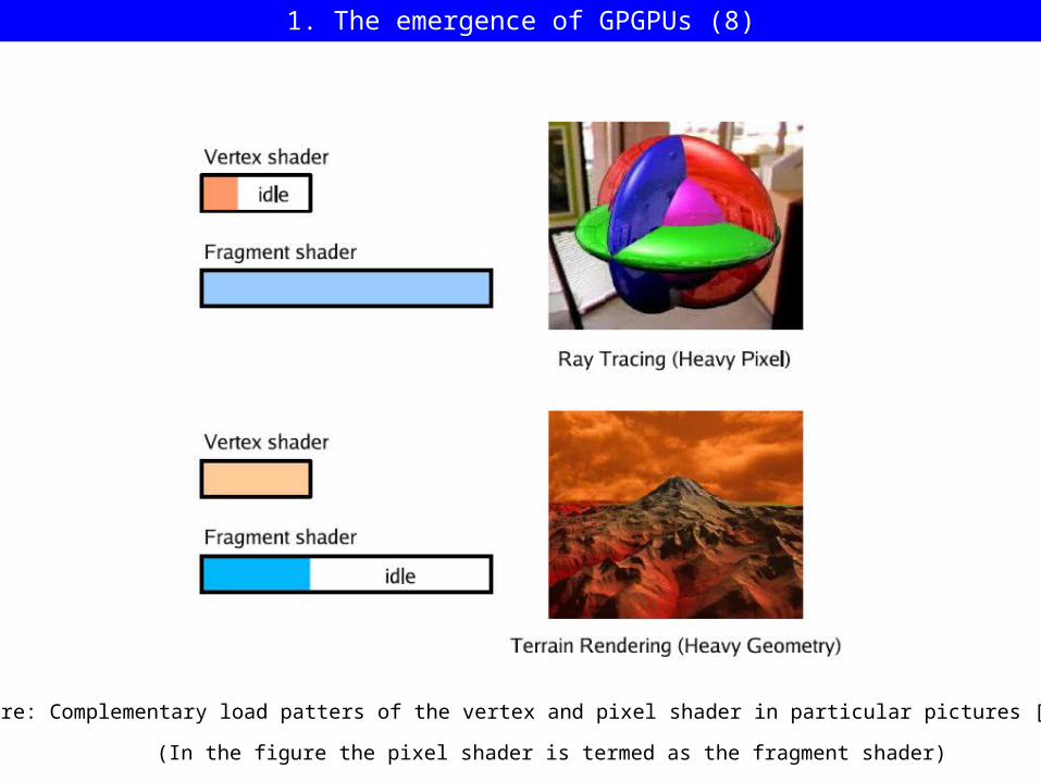
Figure: Complementary load patters of the vertex and pixel shader in particular pictures [21]
(In the figure the pixel shader is termed as the fragment shader)
1. The emergence of GPGPUs (8)

Figure: Rendering pipeline history [23]
1. The emergence of GPGPUs (9)

Figure: Principle of the unified shader architecture [22]
1. The emergence of GPGPUs (10)

Unified shader model (introduced in the SM 4.0 of DirectX 10.0)
The same (programmable) processor can be used to implement all shaders;
• the vertex shader• the pixel shader and• the geometry shader (new feature of the SMl 4)
Unified, programable shader architecture
1. The emergence of GPGPUs (11)

The unified shader performs an inherent load balancing while executing the vertex and pixel shader operations [21] on the same hardware.
(For further benefits of SM4 see [20], [21].
1. The emergence of GPGPUs (12)

Figure: Different loading of separately implemented shaders vs load balancing in a unified shader in particular pictures [21]
(In the figure the pixel shader is termed as the fragment shader)
1. The emergence of GPGPUs (13)

First GPUs with unified shader architecture
Predecessor
ATI Tecnologies R500 (codename: Xenos) (11/2005)
• Used in Microsoft’s Xbox 360 console.• Supports SM 3.O (of DirectX 9.0c)• Has 48 unified shader units.
First consumer GPU
Nvidia’s G80 (11/2006)
• Used in the 8800 GTX and 8800 GTS graphics cards• Supports SM 4.0 ( of DirectX 10)• Has 128 shader units (designated as Streaming processors)
1. The emergence of GPGPUs (14)

Based on its FP32 computing capability and the large number of FP-units available
the unified shader is a prospective candidate for speeding up HPC!
GPUs with unified shader architectures also termed as
GPGPUs
(General Purpose GPUs)
1. Introduction (1)

Figure: Peak SP FP performance of Nvidia’s GPUs vs Intel’ P4 and Core2 processors [11]
1. Introduction (2)

Figure: Bandwidth values of Nvidia’s GPU’s vs Intel’s P4 and Core2 processors [11]
1. Introduction (3)

Not cached
Figure: Contrasting the utilization of the silicon area in CPUs and GPUs [11]
1. Introduction (4)

2. Basics of the SIMT execution
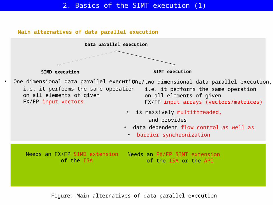
Main alternatives of data parallel execution
Data parallel execution
SIMD execution SIMT execution
• One dimensional data parallel execution, i.e. it performs the same operation on all elements of given FX/FP input vectors
• One/two dimensional data parallel execution, i.e. it performs the same operation on all elements of given FX/FP input arrays (vectors/matrices)
E.g. 2. and 3. generationsuperscalars
GPGPUs,data parallel accelerators
Figure: Main alternatives of data parallel execution
• data dependent flow control as well as • barrier synchronization
• is massively multithreaded, and provides
Needs an FX/FP SIMD extension of the ISA
Needs an FX/FP SIMT extension of the ISA or the API
2. Basics of the SIMT execution (1)

Scalar execution SIMD execution SIMT execution
Domain of execution:single data elements
Domain of execution:elements of vectors
Domain of execution:elements of matrices
(at the programming level)
Figure: Domains of execution in case of scalar, SIMD and SIMT execution
2. Basics of the SIMT execution (2)
Remark
SIMT execution is also termed as SPMD (Single_Program Multiple_Data) execution (Nvidia)

Key components of the implementation of SIMT execution
• Data parallel execution
• Massive multithreading
• Data dependent flow control
• Barrier synchronization
2. Basics of the SIMT execution (3)

(i.e. all ALUs of a SIMT core perform typically the same operation).
Data parallel execution
Fetch/Decode
ALU ALU ALUALU
SIMT core
Figure: Basic layout of a SIMT core
ALU ALU ALUALU
Performed by SIMT cores
SIMT cores execute the same instruction stream on a number of ALUs
SIMT cores are the basic building blocks of GPGPU or data parallel accelerators.
2. Basics of the SIMT execution (4)
During SIMT execution 2-dimensional matrices will be mapped to blocks of SIMT cores.
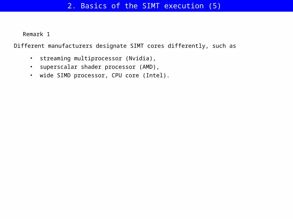
• streaming multiprocessor (Nvidia), • superscalar shader processor (AMD),• wide SIMD processor, CPU core (Intel).
Remark 1
Different manufacturers designate SIMT cores differently, such as
2. Basics of the SIMT execution (5)

Fetch/Decode
ALU ALU ALUALU
RF RF RF RF
Each ALU is allocated a working register set (RF)
Figure: Main functional blocks of a SIMT core
ALU ALU ALUALU
RFRFRFRF
2. Basics of the SIMT execution (6)

SIMT ALUs perform typically, RRR operations, that is
ALUs take their operands from and write the calculated results to the register set (RF) allocated to them.
ALU
RF
Figure: Principle of operation of the SIMD ALUs
2. Basics of the SIMT execution (7)

Remark 2
ALU
RF RF RF RF RF RF RF RF
ALU ALU ALUALU ALU ALUALU ALU ALUALU ALU
Figure: Allocation of distinct parts of a large register set as workspaces of the ALUs
Actually, the register sets (RF) allocated to each ALU are given parts of a large enough register file.
2. Basics of the SIMT execution (8)

Basic operation of recent SIMT ALUs
ALU
RF
• are pipelined, capable of starting a new operation every new clock cycle, (more precisely, every shader clock cycle),
• execute basically SP FP-MADD (simple precision i.e. 32-bit. Multiply-Add) instructions of the form axb+c ,
• need a few number of clock cycles, e.g. 4 shader cycles, to present the results of the SP FMADD operations to the RF,
That is, without further enhancements their peak performance is 2 SP FP operations/cycle
2. Basics of the SIMT execution (9)
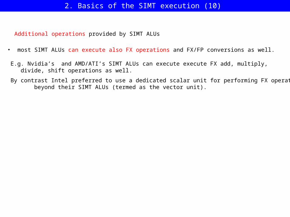
Additional operations provided by SIMT ALUs
• most SIMT ALUs can execute also FX operations and FX/FP conversions as well.
E.g. Nvidia’s and AMD/ATI’s SIMT ALUs can execute execute FX add, multiply, divide, shift operations as well.
By contrast Intel preferred to use a dedicated scalar unit for performing FX operations beyond their SIMT ALUs (termed as the vector unit).
2. Basics of the SIMT execution (10)
Enhancements of SIMT cores
Typically, beyond a number of identical SIMD ALUs (designated occasionally as the vector unit) SIMT cores include also
one or more dedicated units to speed up special computations not supported by the SIMD ALUs, such as
Examples
• double precision (DP) FP operations,• trigonometric functions, such as sin, cos, etc.
most recent GPGPU cores of Nvidia and AMD/ATI (GT200, RV770)
2. Basics of the SIMT execution (11)

Massive multithreading
Multithreading is implemented by
creating and managing parallel executable threads for each data element of the execution domain.
Figure: Parallel executable threads for each element of the execution domain
Same instructions for all data elements
2. Basics of the SIMT execution (12)
Aim of multithreading
Speeding up computations
• by increased utilization of available computing resources in case when threads stall due to long latency operations,
(achieved by suspending stalled threads from execution and allocating free computing resources to runable threads)
• by increased utilization of available silicon area for performing computations rather than for implementing sophisticated cache systems,
(achieved by hiding memory access latencies through multithreading)
2. Basics of the SIMT execution (13)

Effective implementation of multithreading
when thread switches, called context switches, do not cause cycle penalties.
• providing and maintaining separate contexts for each thread, and
• implementing a zero-cycle context switch mechanism.
Achieved by
2. Basics of the SIMT execution (14)

ALUALU ALU ALUALU ALU ALUALU ALU ALUALU ALU
CTX CTX CTX CTX CTX CTX CTXCTX
CTX CTX CTX CTX CTX CTX CTXCTX
CTX CTX CTX CTX CTX CTX CTXCTX
CTX CTX CTX CTX CTX CTX CTXCTX
CTX CTX CTX CTX CTX CTX CTXCTX
CTX CTX CTX CTX CTX CTX CTXCTX
Actual context Register file (RF)
Context switch
Figure: Providing separate thread contexts for each thread allocated for execution in a SIMT ALU
Fetch/Decode
SIMT core
2. Basics of the SIMT execution (15)
Data dependent flow control
SIMT branches allow data dependent thread execution.
In SIMT processing both paths of a branch are executed such that
for each path the prescribed operations are executed on all data elements which obey the data condition valid for that path (e.g. xi > 0).
Example
2. Basics of the SIMT execution (16)

Figure: Execution of branches [24]
The given condition will be checked separately for each thread
2. Basics of the SIMT execution (17)

Figure: Execution of branches [24]
First all ALUs meeting the condition execute the prescibed three operations,then all ALUs missing the condition execute the next two operatons
2. Basics of the SIMT execution (18)

Figure: Resuming instruction stream processing after executing a branch [24]
2. Basics of the SIMT execution (19)

Barrier synchronization
Implemented in AMD’s Intermediate Language (IL) by the fence_threads instruction [10].
In the R600 ISA this instruction is coded by setting the BARRIER field of the Control Flow (CF) instruction format [7].
Remark
Allows to let complete all prior instructions before executing the next instruction.
2. Basics of the SIMT execution (20)

3. Overview of GPGPUs

Basic implementation alternatives of the SIMT execution
GPGPUs Data parallel accelerators
Dedicated units supporting data parallel execution
with appropriate programming environment
Programmable GPUs with appropriate
programming environments
E.g. Nvidia’s 8800 and GTX linesAMD’s HD 38xx, Hd48xx lines
Nvidia’s Tesla linesAMD’s FireStream lines
Have display outputs No display outputsHave larger memories than GPGPUs
Figure: Basic implementation alternatives of the SIMT execution
3. Overview of GPGPUs (1)

GPGPUs
Nvidia’s line AMD/ATI’s line
Figure: Overview of Nvidia’s and AMD/ATI’s GPGPU lines
90 nm G80
65 nm G92 G200
Shrink Enhanced arch.
80 nm R600
55 nm RV670 RV770
Shrink Enhanced arch.
3. Overview of GPGPUs (2)

48 ALUs
6/08
65 nm/1400 mtrs
11/06
90 nm/681 mtrs
Cores
Cards
CUDA
Cores
G80
2005 2006 2007 2008
96 ALUs320-bit
8800 GTS
10/07
65 nm/754 mtrs
G92
128 ALUs384-bit
8800 GTX
112 ALUs256-bit
8800 GT
GT200
192 ALUs448-bit
GTX260
240 ALUs512-bit
GTX280
6/07
Version 1.0
11/07
Version 1.1
6/08
Version 2.0
5/08
55 nm/956 mtrs
5/07
80 nm/681 mtrs
R600
11/07
55 nm/666 mtrs
R670 RV770
11/05
R500
320 ALUs512-bit
HD 2900XT
320 ALUs256-bit
HD 3850
320 ALUs256-bit
HD 3870
800 ALUs256-bit
HD 4850
800 ALUs256-bit
HD 4870Cards (Xbox)
11/07
Brook+Brooks+
RapidMind
2009
NVidia
AMD/ATI
6/08
support
3870
Figure: Overview of GPGPUs
3. Overview of GPGPUs (3)

8800 GTS 8800 GTX 8800 GT GTX 260 GTX 280
Core G80 G80 G92 GT200 GT200
Introduction 11/06 11/06 10/07 6/08 6/08
IC technology 90 nm 90 nm 65 nm 65 nm 65 nm
Nr. of transistors 681 mtrs 681 mtrs 754 mtrs 1400 mtrs 1400 mtrs
Die are 480 mm2 480 mm2 324 mm2 576 mm2 576 mm2
Core frequency 500 MHz 575 MHz 600 MHz 576 MHz 602 MHz
Computation
No. stream proc.s 96 128 112 192 240
Shader frequency 1.2 GHz 1.35 GHz 1.512 GHz 1.242 GHz 1.296 GHz
No. FP32 inst./cycle 3* (but only in a few issue cases) 3 3
Peak FP32 performance 346 GLOPS 512 GLOPS 508 GLOPS 715 GLOPS 933 GLOPS
Peak FP64 performance – – – – 77/76 GLOPS
Memory
Mem. transfer rate (eff) 1600 Mb/s 1800 Mb/s 1800 Mb/s 1998 Mb/s 2214 Mb/s
Mem. interface 320-bit 384-bit 256-bit 448-bit 512-bit
Mem. bandwidth 64 GB/s 86.4 GB/s 57.6 GB/s 111.9 GB/s 141.7 GB/s
Mem. size 320 MB 768 MB 512 MB 896 MB 1.0 GB
Mem. type GDDR3 GDDR3 GDDR3 GDDR3 GDDR3
Mem. channel 6*64-bit 6*64-bit 4*64-bit 8*64-bit 8*64-bit
Mem. contr. Crossbar Crossbar Crossbar Crossbar Crossbar
System
Multi. CPU techn. SLI SLI SLI SLI SLI
Interface PCIe x16 PCIe x16 PCIe 2.0x16 PCIe 2.0x16 PCIe 2.0x16
MS Direct X 10 10 10 10.1 subset 10.1 subset
Table: Main features of Nvidia’s GPGPUs
3. Overview of GPGPUs (4)

HD 2900XT HD 3850 HD 3870 HD 4850 HD 4870
Core R600 R670 R670 RV770 RV770
Introduction 5/07 11/07 11/07 5/08 5/08
IC technology 80 nm 55 nm 55 nm 55 nm 55 nm
Nr. of transistors 700 mtrs 666 mtrs 666 mtrs 956 mtrs 956 mtrs
Die are 408 mm2 192 mm2 192 mm2 260 mm2 260 mm2
Core frequency 740 MHz 670 MHz 775 MHz 625 MHz 750 MHz
Computation
No. stream proc.s 320 320 320 800 800
Shader frequency 740 MHz 670 MHz 775 MHz 625 MHz 750 MHz
No. FP32 inst./cycle 2 2 2 2 2
Peak FP32 performance 471.6 GLOPS 429 GLOPS 496 GLOPS 1000 GLOPS 1200 GLOPS
Peak FP64 performance – – – 200 GLOPS 240 GLOPS
Memory
Mem. transfer rate (eff) 1600 Mb/s 1660 Mb/s 2250 Mb/s 2000 Mb/s 3600 Mb/s (GDDR5)
Mem. interface 512-bit 256-bit 256-bit 265-bit 265-bit
Mem. bandwidth 105.6 GB/s 53.1 GB/s 720 GB/s 64 GB/s 118 GB/s
Mem. size 512 MB 256 MB 512 MB 512 MB 512 MB
Mem. type GDDR3 GDDR3 GDDR4 GDDR3 GDDR3/GDDR5
Mem. channel 8*64-bit 8*32-bit 8*32-bit 4*64-bit 4*64-bit
Mem. contr. Ring bus Ring bus Ring bus Crossbar Crossbar
System
Multi. CPU techn. CrossFire CrossFire X CrossFire X CrossFire X CrossFire X
Interface PCIe x16 PCIe 2.0x16 PCIe 2.0x16 PCIe 2.0x16 PCIe 2.0x16
MS Direct X 10 10.1 10.1 10.1 10.1
Table: Main features of AMD/ATIs GPGPUs
3. Overview of GPGPUs (5)
Price relations (as of 10/2008)
Nvidia
GTX260 ~ 300 $GTX280 ~ 600 $
AMD/ATI
HD4850 ~ 200 $HD4870 na
3. Overview of GPGPUs (6)

Implementation alternatives of data parallel accelerators
On-dieintegration
On card implementation
Recent implementations
Futureimplementations
E.g. GPU cards
Data-parallelaccelerator cards
Intel’s Heavendahl
AMD’s Torrenzaintegration technology
AMD’s Fusionintegration technology
Trend
Figure: Implementation alternatives of dedicated data parallel accelerators
Data parallel accelerators
3. Overview of GPGPUs (7)

4. Overview of data parallel accelerators

On-card accelerators
1U serverimplementations
Cardimplementations
Desktopimplementations
Usually dual cardsmounted into a box,
connected to anadapter card
that is inserted into a free PCI-E x16 slot of the host PC through a cable.
E.g. Nvidia Tesla D870 Nvidia Tesla S870Nvidia Tesla S1070AMD FireStream 9250
Nvidia Tesla C870Nvidia Tesla C1060AMD FireStream 9170
Usually 4 cards mounted into a 1U server rack,connected two adapter cards
that are inserted into two free PCIEx16 slots of a server
through two switches and two cables.
Single cards fittinginto a free PCI Ex16 slotof the host computer.
Figure:Implementation alternatives of on-card accelerators
4. Overview of data parellel accererators (1)

Figure: Main functional units of Nvidia’s Tesla C870 card [2]
FB: Frame Buffer
4. Overview of data parellel accererators (2)

Figure: Nvida’s Tesla C870 and AMD’s FireStream 9170 cards [2], [3]
4. Overview of data parellel accererators (3)

Figure: Tesla D870 desktop implementation [4]
4. Overview of data parellel accererators (4)

Figure: Nvidia’s Tesla D870 desktop implementation [4]
4. Overview of data parellel accererators (5)

Figure: PCI-E x16 host adapter card of Nvidia’s Tesla D870 desktop [4]
4. Overview of data parellel accererators (6)
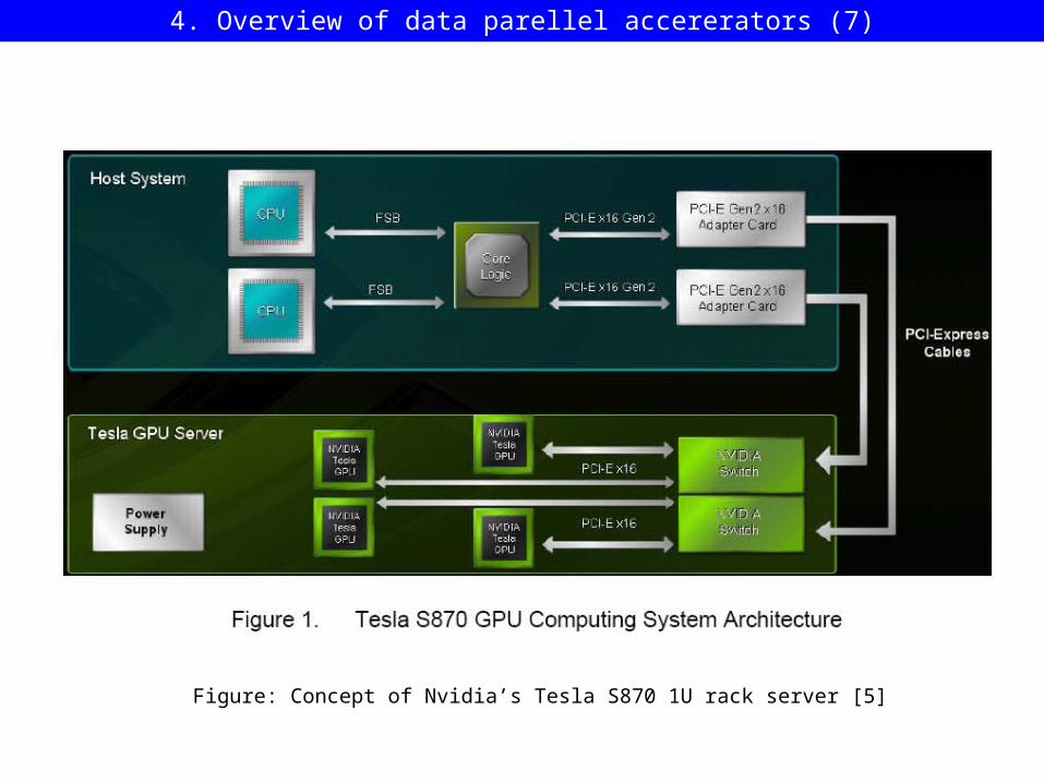
Figure: Concept of Nvidia’s Tesla S870 1U rack server [5]
4. Overview of data parellel accererators (7)

Figure: Internal layout of Nvidia’s Tesla S870 1U rack [6]
4. Overview of data parellel accererators (8)

Figure: Connection cable between Nvidia’s Tesla S870 1U rack and the adapter cards
inserted into PCI-E x16 slots of the host server [6]
4. Overview of data parellel accererators (9)

6/08
GT200-based4 GB GDDR30.936 GLOPS
6/07
G80-based1.5 GB GDDR30.519 GLOPS
Card
Desktop
IU Server
C870
2007 2008
C1060
CUDA
NVidia Tesla
6/07
G80-based2*C870 incl.3 GB GDDR31.037 GLOPS
D870
6/07
G80-based4*C870 incl.6 GB GDDR32.074 GLOPS
S870
6/07
Version 1.0
6/08
GT200-based4*C1060
16 GB GDDR33.744 GLOPS
S1070
11/07
Version 1.01
6/08
Version 2.0
Figure: Overview of Nvidia’s Tesla family
4. Overview of data parellel accererators (10)

6/08
Shipped
11/07
RV670-based2 GB GDDR3
500 GLOPS FP32~200 GLOPS FP64
Card
Stream Computing SDK
9170
2007 2008
9170
Rapid Mind
AMD FireStream
6/08
RV770-based1 GB GDDR31 TLOPS FP32
~300 GFLOPS FP64
9250
12/07
Brook+ACM/AMD Core Math LibraryCAL (Computer Abstor Layer)
Version 1.0
10/08
Shipped
9250
Figure: Overview of AMD/ATI’s FireStream family
4. Overview of data parellel accererators (11)
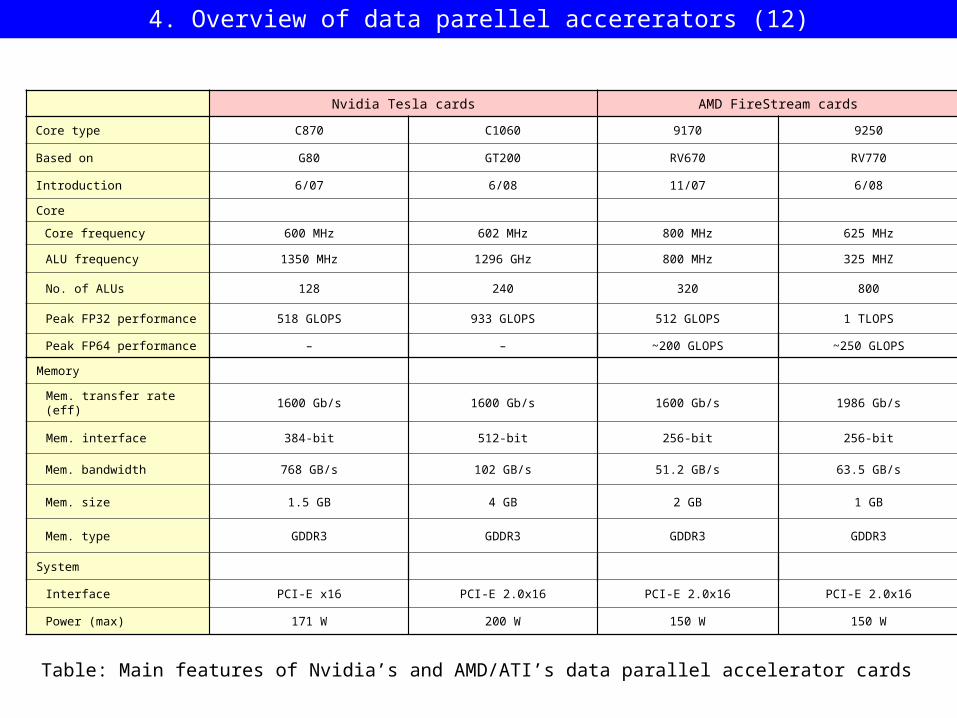
Nvidia Tesla cards AMD FireStream cards
Core type C870 C1060 9170 9250
Based on G80 GT200 RV670 RV770
Introduction 6/07 6/08 11/07 6/08
Core
Core frequency 600 MHz 602 MHz 800 MHz 625 MHz
ALU frequency 1350 MHz 1296 GHz 800 MHz 325 MHZ
No. of ALUs 128 240 320 800
Peak FP32 performance 518 GLOPS 933 GLOPS 512 GLOPS 1 TLOPS
Peak FP64 performance – – ~200 GLOPS ~250 GLOPS
Memory
Mem. transfer rate (eff) 1600 Gb/s 1600 Gb/s 1600 Gb/s 1986 Gb/s
Mem. interface 384-bit 512-bit 256-bit 256-bit
Mem. bandwidth 768 GB/s 102 GB/s 51.2 GB/s 63.5 GB/s
Mem. size 1.5 GB 4 GB 2 GB 1 GB
Mem. type GDDR3 GDDR3 GDDR3 GDDR3
System
Interface PCI-E x16 PCI-E 2.0x16 PCI-E 2.0x16 PCI-E 2.0x16
Power (max) 171 W 200 W 150 W 150 W
Table: Main features of Nvidia’s and AMD/ATI’s data parallel accelerator cards
4. Overview of data parellel accererators (12)

Price relations (as of 10/2008)
Nvidia Tesla
C870 ~ 1500 $D870 ~ 5000 $S870 ~ 7500 $
C1060 ~ 1600 $
S1070 ~ 8000 $
AMD/ATI FireStream
9170 ~ 800 $ 9250 ~ 800 $
4. Overview of data parellel accererators (13)

5. Microarchitecture and operation
5.1 Nvidia’s GPGPU line
5.2 AMD/ATI’s GPGPU line
5.3 Intel’s Larrabee
5.1 Nvidia’s GPGPU line

Microarchitecture of GPGPUs
3-levelmicroarchitectures
Two-level microarchitectures
Dedicated microarchitecturesa priory developed to support
both graphics and HPC
Microarchitectures inheriting the structure of
programmable GPUs
E.g. Nvidia’s and AMD/ATI’sGPGPUs
Intel’sLarrabee
Figure: Alternative layouts of microarchitectures of GPGPUs
Microarchitecture of GPUs
5.1 Nvidia’s GPGPU line (1)

Cores
L1 Cache
Cores
L1 Cache1 n
IN
L2
MC
L2
MC
Global MemoryH
ub
Dis
pla
y c.
Work Schedeler
Command Processor Unit
North Bridge Host memoryHost CPU
Commands
CBA
Data
2x32-bit 2x32-bit
1 m
CB CB
CB: Core Blocks
CBA: Core Block Array
IN: Interconnection Network
MC: Memory Controller
5.1 Nvidia’s GPGPU line (2)
PCI-E x 16 IF
Simplified block diagram of recent 3-level GPUs/data-parallel accelerators(Data parallel accelerators do not include Display controllers)

In these slides Nvidia AMD/ATI
CCoreSIMT Core
SMStreaming Multiprocesszor Multithreaded processor
Shader-processzorThread processor
CB Core Block TPCTexture Processor ClusterMultiprocessor
SIMD ArraySIMD EngineSIMD coreSIMD
CBA Core Block Array SPA Streaming Processor Array
ALU Algebraic Logic UnitStreaming ProcessorThread ProcessorScalar ALU
Stream Processing UnitStream Processor
Table: Terminologies used with GPGPUs/Data parallel accelerators
5.1 Nvidia’s GPGPU line (3)

Microarchitecture of Nvidia’s GPGPUs
GPGPUs based on 3-level microarchitectures
Nvidia’s line AMD/ATI’s line
Figure: Overview of Nvidia’s and AMD/ATI’s GPGPU lines
90 nm G80
65 nm G92 G200
Shrink Enhanced arch.
80 nm R600
55 nm RV670 RV770
Shrink Enhanced arch.
5.1 Nvidia’s GPGPU line (4)
G80/G92
5.1 Nvidia’s GPGPU line (5)
Microarchitecture
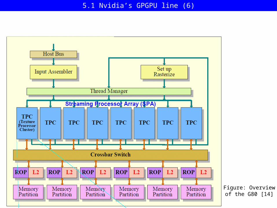
Figure: Overviewof the G80 [14]
5.1 Nvidia’s GPGPU line (6)

Figure: Overviewof the G92 [15]
5.1 Nvidia’s GPGPU line (7)

Figure: The Core Block of theG80/G92 [14], [15]
5.1 Nvidia’s GPGPU line (8)

Figure: Block diagramof G80/G92 cores
[14], [15]
Streaming Processors:SIMT ALUs
5.1 Nvidia’s GPGPU line (9)

8K registers (each 4 bytes wide) deliver 4 operands/clock
Load/Store pipe can also read/write RF
I$L1
MultithreadedInstruction Buffer
RF
C$L1
SharedMem
Operand Select
MAD SFU
SM Register File (RF)
Figure: Register File [12]
Individual components of the core
5.1 Nvidia’s GPGPU line (10)
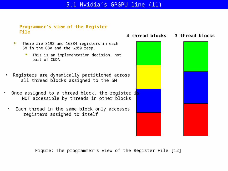
Programmer’s view of the Register File
There are 8192 and 16384 registers in each SM in the G80 and the G200 resp.
This is an implementation decision, not part of CUDA
4 thread blocks 3 thread blocks
• Registers are dynamically partitioned across all thread blocks assigned to the SM
• Once assigned to a thread block, the register is NOT accessible by threads in other blocks
• Each thread in the same block only accesses registers assigned to itself
Figure: The programmer’s view of the Register File [12]
5.1 Nvidia’s GPGPU line (11)
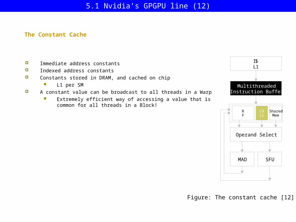
The Constant Cache
Immediate address constants Indexed address constants Constants stored in DRAM, and cached on chip
L1 per SM A constant value can be broadcast to all threads in a Warp
Extremely efficient way of accessing a value that is common for all threads in a Block!
I$L1
MultithreadedInstruction Buffer
RF
C$L1
SharedMem
Operand Select
MAD SFU
Figure: The constant cache [12]
5.1 Nvidia’s GPGPU line (12)

Shared Memory
Each SM has 16 KB of Shared Memory 16 banks of 32 bit words
CUDA uses Shared Memory as shared storage visible to all threads in a thread block
read and write access Not used explicitly for pixel shader programs
I$L1
MultithreadedInstruction Buffer
RF
C$L1
SharedMem
Operand Select
MAD SFU
Figure: Shared Memory [12]
5.1 Nvidia’s GPGPU line (13)

A program needs to manage the global, constant and texture memory spaces visible to kernels through calls to the CUDA runtime.
This includes memory allocation and deallocation as well as invoking data transfers between the CPU and GPU.
5.1 Nvidia’s GPGPU line (14)
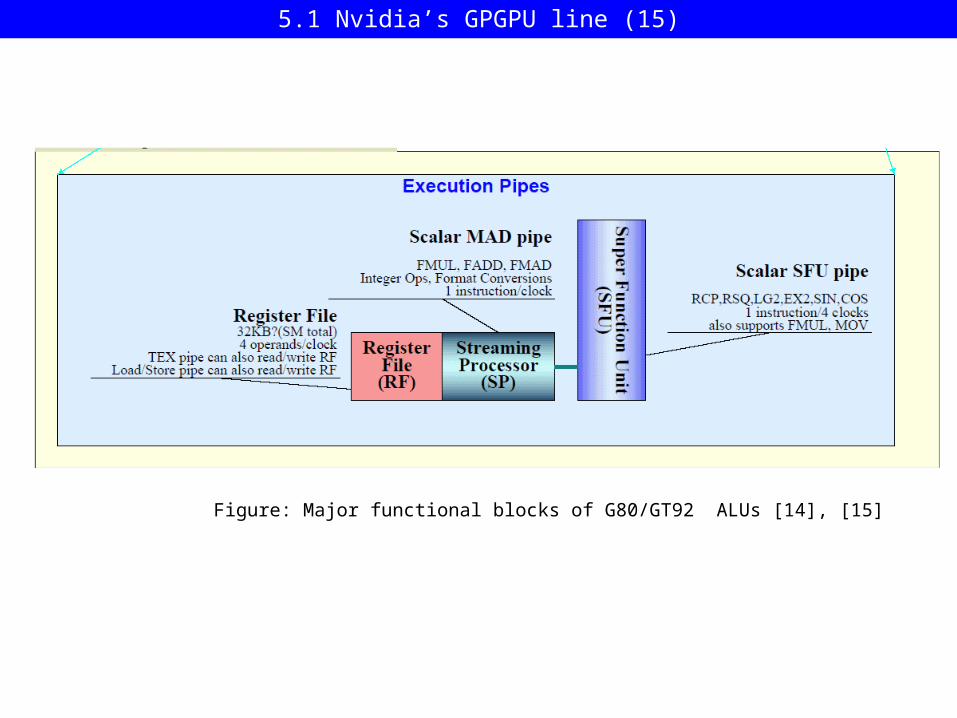
Figure: Major functional blocks of G80/GT92 ALUs [14], [15]
5.1 Nvidia’s GPGPU line (15)
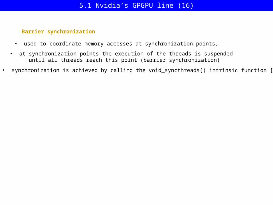
Barrier synchronization
• synchronization is achieved by calling the void_syncthreads() intrinsic function [11];
• used to coordinate memory accesses at synchronization points,
• at synchronization points the execution of the threads is suspended until all threads reach this point (barrier synchronization)
5.1 Nvidia’s GPGPU line (16)

Based on Nvidia’s data parallel computing model
Principle of operation
Nvidia’s data parallel computing model is specified at different levels of abstraction
• at the Instruction Set Architecture level (ISA) (not disclosed)
• at the intermediate level (at the level of APIs) not discussed here)
• at the high level programming language level by means of CUDA.
5.1 Nvidia’s GPGPU line (17)

CUDA [11]
• programming language and programming environment that allows explicit data parallel execution on an attached massively parallel device (GPGPU),
• its underlying principle is to allow the programmer to target portions of the source code for execution on the GPGPU,
• defined as a set of C-language extensions,
The key element of the language is the notion of kernel
5.1 Nvidia’s GPGPU line (18)

A kernel is specified by
• using the _global_ declaration specifier,• a number of associated CUDA threads, • a domain of execution (grid, blocks) using the syntax <<<….>>>
Execution of kernels
when called, a kernel is executed N times in parallel by N associated CUDA threads, as opposed to only once like in case of regular C functions.
5.1 Nvidia’s GPGPU line (19)

Example
• adds two vectors A and B of size N and• stores the result into vector C
Remark
The thread index threadIdx is a vector of up to 3-components, that identifies a one-, two- or three-dimensional thread block.
The above sample code
by executing the invoked threads (identified by a one dimensional index i) in parallel on the attached massively parallel GPGPU, rather than adding the vectors A and B by executing embedded loops on the conventional CPU.
5.1 Nvidia’s GPGPU line (20)

The kernel concept is enhanced by three key abstractions
• the thread concept,• the memory concept and • the synchronization concept.
5.1 Nvidia’s GPGPU line (21)

The thread concept
based on a three level hierarchy of threads
• grids• thread blocks• threads
5.1 Nvidia’s GPGPU line (22)

Each kernel invocation is executed as a grid ofthread blocks (Block(i,j))kernel0<<<>>>()
kernel1<<<>>>()
Host Device
Figure: Hierarchy of threads [25]
The hierarchy of threads
5.1 Nvidia’s GPGPU line (23)
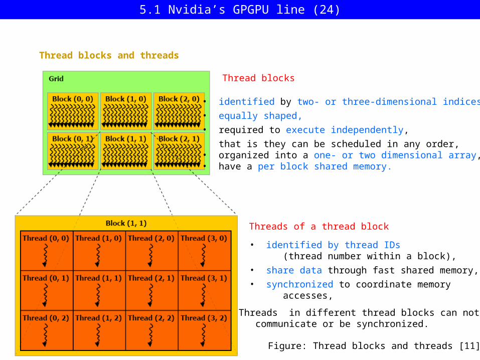
Thread blocks
• identified by two- or three-dimensional indices,
• equally shaped,
• required to execute independently,
that is they can be scheduled in any order,• organized into a one- or two dimensional array, • have a per block shared memory.
Figure: Thread blocks and threads [11]
Threads of a thread block
• identified by thread IDs (thread number within a block),
• share data through fast shared memory,
• synchronized to coordinate memory accesses,
Threads in different thread blocks can not communicate or be synchronized.
Thread blocks and threads
5.1 Nvidia’s GPGPU line (24)

• private registers (R/W access)• per block shared memory (R/W access)• per grid global memory (R/W access)• per block constant memory (R access)• per TPC texture memory (R access)
Threads have
The global, constant and texture memory spaces can be read from or written to by the CPU and are persistent across kernel launches by the same application.
Shared memory is organized into banks (16 banks in version 1)
Figure: Memory concept [26] (revised)
The memory concept
5.1 Nvidia’s GPGPU line (25)

Mapping of the memory spaces of the programming model to the memory spaces of the streaming processor
Streaming Multiprocessor 1 (SM 1)
A thread block is scheduled for execution to a particular multithreaded SM
An SM incorporates 8 Execution Units (designated a Processors in the figure)
SMs are the fundamental processing units for CUDA thread blocks
Figure: Memory spaces of the SM [7]
5.1 Nvidia’s GPGPU line (26)

The synchronization concept
• synchronization is achieved by the declaration void_syncthreads();
• used to coordinate memory accesses at synchronization points,
• at synchronization points the execution of the threads is suspended until all threads reach this point (barrel synchronization)
Barrier synchronization
5.1 Nvidia’s GPGPU line (27)

GT200
5.1 Nvidia’s GPGPU line (28)

Figure: Block diagram of the GT200 [16]
5.1 Nvidia’s GPGPU line (29)

Figure: The Core Block of theGT200 [16]
5.1 Nvidia’s GPGPU line (30)
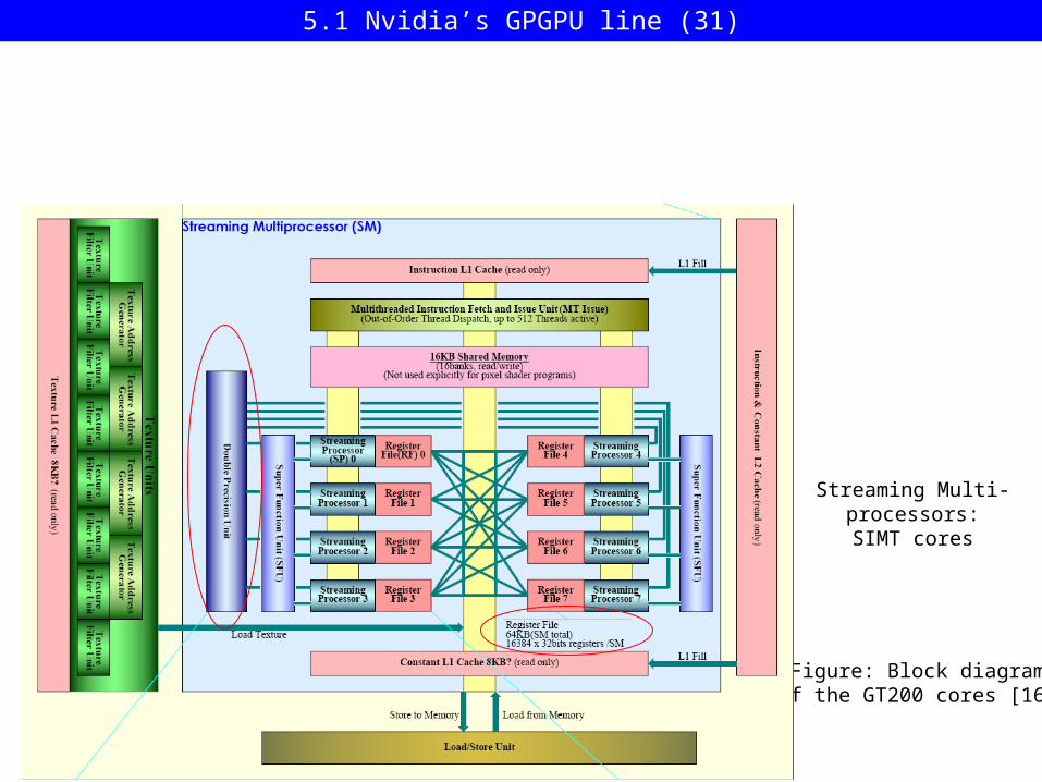
Figure: Block diagramof the GT200 cores [16]
Streaming Multi-processors:SIMT cores
5.1 Nvidia’s GPGPU line (31)

Figure: Major functional blocks of GT200 ALUs [16]
5.1 Nvidia’s GPGPU line (32)

Figure: Die shot of the GT 200 [17]
5.1 Nvidia’s GPGPU line (33)

5.2 Intel’s Larrabee

Larrabee
Part of Intel’s Tera-Scale Initiative.
Project started ~ 2005First unofficial public presentation: 03/2006 (withdrawn) First brief public presentation 09/07 (Otellini) [29] First official public presentations: in 2008 (e.g. at SIGGRAPH [27])Due in ~ 2009
• Performance (targeted): 2 TFlops
• Brief history:
• Objectives:
Not a single product but a base architecture for a number of different products. High end graphics processing, HPC
5.2 Intel’s Larrabee (1)

NI: New Instructions
Figure: Positioning of Larrabeein Intel’s product portfolio [28]
5.2 Intel’s Larrabee (2)
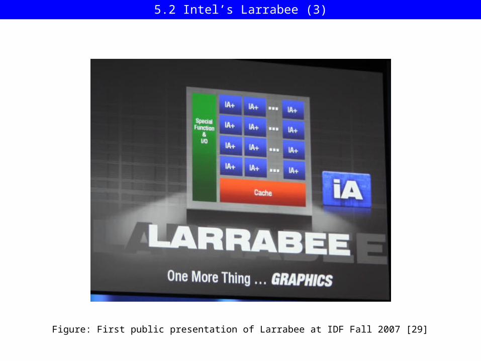
Figure: First public presentation of Larrabee at IDF Fall 2007 [29]
5.2 Intel’s Larrabee (3)

Figure: Block diagram of the Larrabee [30]
Basic architecture
• Cores: In order x86 IA cores augmented with new instructions
• L2 cache: fully coherent
• Ring bus: 1024 bits wide
5.2 Intel’s Larrabee (4)

Figure: Block diagram of Larrabee’s cores [31]
5.2 Intel’s Larrabee (5)

Larrabee’ microarchitecture [27]
Derived from that of the Pentium’s in order design
5.2 Intel’s Larrabee (6)

Figure: The anchestor of Larrabee’s cores [28]
• 64-bit instructions
• 4-way multithreaded (with 4 register sets)
• addition of a 16-wide (16x32-bit) VU • increased L1 caches (32 KB vs 8 KB)
• access to its 256 KB local subset of a coherent L2 cache
• ring network to access the coherent L2 $ and allow interproc. communication.
Main extensions
5.2 Intel’s Larrabee (7)

New instructions allow explicit cache control
the L2 cache can be used as a scratchpad memory while remaining fully coherent.
• to prefetch data into the L1 and L2 caches• to control the eviction of cache lines by reducing their priority.
5.2 Intel’s Larrabee (8)

The Scalar Unit
• supports the full ISA of the Pentium (it can run existing code including OS kernels and applications)
• bit count• bit scan (it finds the next bit set within a register).
• provides new instructions, e.g. for
5.2 Intel’s Larrabee (9)

Figure: Block diagram of the Vector Unit [31]
The Vector Unit
VU scatter-gather instructions
(load a VU vector register from 16 non-contiguous data locations from anywhere from the on die L1 cache without penalty, or store a VU register similarly).
8-bit, 16-bit integer and 16 bit FP data can be read from the L1 $ or written into the L1 $, with conversion to 32-bit integers without penalty.
Numeric conversions
L1 D$ becomesas an extension of the register file
Mask registers
have one bit per bit lane,to control which bits of a vector reg.or memory data are read or writtenand which remain untouched.
5.2 Intel’s Larrabee (10)

Figure: Layout of the 16-wide vector ALU [31]
• ALUs execute integer, SP and DP FP instructions• Multiply-add instructions are available.
ALUs
5.2 Intel’s Larrabee (11)

Task scheduling
performed entirely by software rather than by hardware, like in Nvidia’s or AMD/ATI’s GPGPUs.
5.2 Intel’s Larrabee (12)

SP FP performance
2 operations/cycle16 ALUs
32 operations/core
At present no data available for the clock frequency or the number of cores in Larrabee.
Assuming a clock frequency of 2 GHz and 32 cores
SP FP performance: 2 TFLOPS
5.2 Intel’s Larrabee (13)

Figure: Larrabee’s software stack (Source Intel)
Larrabee’s Native C/C++ compiler allows many available apps to be recompiled and run correctly with no modifications.
5.2 Intel’s Larrabee (14)

6. References
[2]: NVIDIA Tesla C870 GPU Computing Board, Board Specification, Jan. 2008, Nvidia
[1]: Torricelli F., AMD in HPC, HPC07, http://www.altairhyperworks.co.uk/html/en-GB/keynote2/Torricelli_AMD.pdf
[3] AMD FireStream 9170, http://ati.amd.com/technology/streamcomputing/product_firestream_9170.html
[4]: NVIDIA Tesla D870 Deskside GPU Computing System, System Specification, Jan. 2008, Nvidia, http://www.nvidia.com/docs/IO/43395/D870-SystemSpec-SP-03718-001_v01.pdf
[5]: Tesla S870 GPU Computing System, Specification, Nvida, http://jp.nvidia.com/docs/IO/43395/S870-BoardSpec_SP-03685-001_v00b.pdf
[6]: Torres G., Nvidia Tesla Technology, Nov. 2007, http://www.hardwaresecrets.com/article/495
[7]: R600-Family Instruction Set Architecture, Revision 0.31, May 2007, AMD
[8]: Zheng B., Gladding D., Villmow M., Building a High Level Language Compiler for GPGPU, ASPLOS 2006, June 2008
[9]: Huddy R., ATI Radeon HD2000 Series Technology Overview, AMD Technology Day, 2007 http://ati.amd.com/developer/techpapers.html
[10]: Compute Abstraction Layer (CAL) Technology – Intermediate Language (IL), Version 2.0, Oct. 2008, AMD
6. References (1)
[11]: Nvidia CUDA Compute Unified Device Architecture Programming Guide, Version 2.0, June 2008, Nvidia
[12]: Kirk D. & Hwu W. W., ECE498AL Lectures 7: Threading Hardware in G80, 2007, University of Illinois, Urbana-Champaign, http://courses.ece.uiuc.edu/ece498/al1/ lectures/lecture7-threading%20hardware.ppt#256,1,ECE 498AL Lectures 7: Threading Hardware in G80
[13]: Kogo H., R600 (Radeon HD2900 XT), PC Watch, June 26 2008, http://pc.watch.impress.co.jp/docs/2008/0626/kaigai_3.pdf
[14]: Nvidia G80, Pc Watch, April 16 2007, http://pc.watch.impress.co.jp/docs/2007/0416/kaigai350.htm
[15]: GeForce 8800GT (G92), PC Watch, Oct. 31 2007, http://pc.watch.impress.co.jp/docs/2007/1031/kaigai398_07.pdf
[16]: NVIDIA GT200 and AMD RV770, PC Watch, July 2 2008, http://pc.watch.impress.co.jp/docs/2008/0702/kaigai451.htm
[17]: Shrout R., Nvidia GT200 Revealed – GeForce GTX 280 and GTX 260 Review, PC Perspective, June 16 2008, http://www.pcper.com/article.php?aid=577&type=expert&pid=3
[18]: http://en.wikipedia.org/wiki/DirectX
[19]: Dietrich S., “Shader Model 3.0, April 2004, Nvidia, http://www.cs.umbc.edu/~olano/s2004c01/ch15.pdf
[20]: Microsoft DirectX 10: The Next-Generation Graphics API, Technical Brief, Nov. 2006, Nvidia, http://www.nvidia.com/page/8800_tech_briefs.html
6. References (2)
[21]: Patidar S. & al., “Exploiting the Shader Model 4.0 Architecture, Center for Visual Information Technology, IIIT Hyderabad, http://research.iiit.ac.in/~shiben/docs/SM4_Skp-Shiben-Jag-PJN_draft.pdf
[22]: Nvidia GeForce 8800 GPU Architecture Overview, Vers. 0.1, Nov. 2006, Nvidia, http://www.nvidia.com/page/8800_tech_briefs.html
[24]: Fatahalian K., “From Shader Code to a Teraflop: How Shader Cores Work,” Workshop: Beyond Programmable Shading: Fundamentals, SIGGRAPH 2008,
[25]: Kanter D., “NVIDIA’s GT200: Inside a Parallel Processor,” 09-08-2008
[23]: Graphics Pipeline Rendering History, Aug. 22 2008, PC Watch, http://pc.watch.impress.co.jp/docs/2008/0822/kaigai_06.pdf
[26]: Nvidia CUDA Compute Unified Device Architecture Programming Guide, Version 1.1, Nov. 2007, Nvidia
[27]: Seiler L. & al., “Larrabee: A Many-Core x86 Architecture for Visual Computing,” ACM Transactions on Graphics, Vol. 27, No. 3, Article No. 18, Aug. 2008
[29]: Shrout R., IDF Fall 2007 Keynote, Sept. 18, 2007, PC Perspective, http://www.pcper.com/article.php?aid=453
[28]: Kogo H., “Larrabee”, PC Watch, Oct. 17, 2008, http://pc.watch.impress.co.jp/docs/2008/1017/kaigai472.htm
6. References (3)
[30]: Stokes J., Larrabee: Intel’s biggest leap ahead since the Pentium Pro,” Aug. 04. 2008, http://arstechnica.com/news.ars/post/20080804-larrabee- intels-biggest-leap-ahead-since-the-pentium-pro.html
[31]: Shimpi A. L. C Wilson D., “Intel's Larrabee Architecture Disclosure: A Calculated First Move, Anandtech, Aug. 4. 2008, http://www.anandtech.com/showdoc.aspx?i=3367&p=2
[32]: Hester P., “Multi_Core and Beyond: Evolving the x86 Architecture,” Hot Chips 19, Aug. 2007, http://www.hotchips.org/hc19/docs/keynote2.pdf
[33]: AMD Stream Computing, User Guide, Oct. 2008, Rev. 1.2.1 http://ati.amd.com/technology/streamcomputing/ Stream_Computing_User_Guide.pdf
[34]: Doggett M., Radeon HD 2900, Graphics Hardware Conf. Aug. 2007, http://www.graphicshardware.org/previous/www_2007/presentations/ doggett-radeon2900-gh07.pdf
[35]: Mantor M., “AMD’s Radeon Hd 2900,” Hot Chips 19, Aug. 2007, http://www.hotchips.org/archives/hc19/2_Mon/HC19.03/HC19.03.01.pdf
[36]: Houston M., “Anatomy if AMD’s TeraScale Graphics Engine,”, SIGGRAPH 2008, http://s08.idav.ucdavis.edu/houston-amd-terascale.pdf
[37]: Mantor M., “Entering the Golden Age of Heterogeneous Computing,” PEEP 2008, http://ati.amd.com/technology/streamcomputing/IUCAA_Pune_PEEP_2008.pdf
6. References (4)

[38]: Kogo H., RV770 Overview, PC Watch, July 02 2008, http://pc.watch.impress.co.jp/docs/2008/0702/kaigai_09.pdf
6. References (5)