gmii electrical specification options - ieee802.org · bill quackenbush cisco systems, inc....
TRANSCRIPT
cisco Systems, Inc.Bil l [email protected]
Presentation to IEEE 802.3zMay 14-16, 1997
1
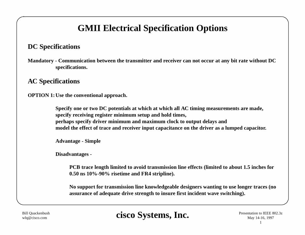
GMII Electrical Specification Options
DC Specifications
Mandatory - Communication between the transmitter and receiver can not occur at any bit rate without DC specifications.
AC Specifications
OPTION 1:Use the conventional approach.
Specify one or two DC potentials at which at which all AC timing measurements are made,specify receiving register minimum setup and hold times,perhaps specify driver minimum and maximum clock to output delays andmodel the effect of trace and receiver input capacitance on the driver as a lumped capacitor.
Advantage - Simple
Disadvantages -
PCB trace length limited to avoid transmission line effects (limited to about 1.5 inches for 0.50 ns 10%-90% risetime and FR4 stripline).
No support for transmission line knowledgeable designers wanting to use longer traces (no assurance of adequate drive strength to insure first incident wave switching).
cisco Systems, Inc.Bil l [email protected]
Presentation to IEEE 802.3zMay 14-16, 1997
2
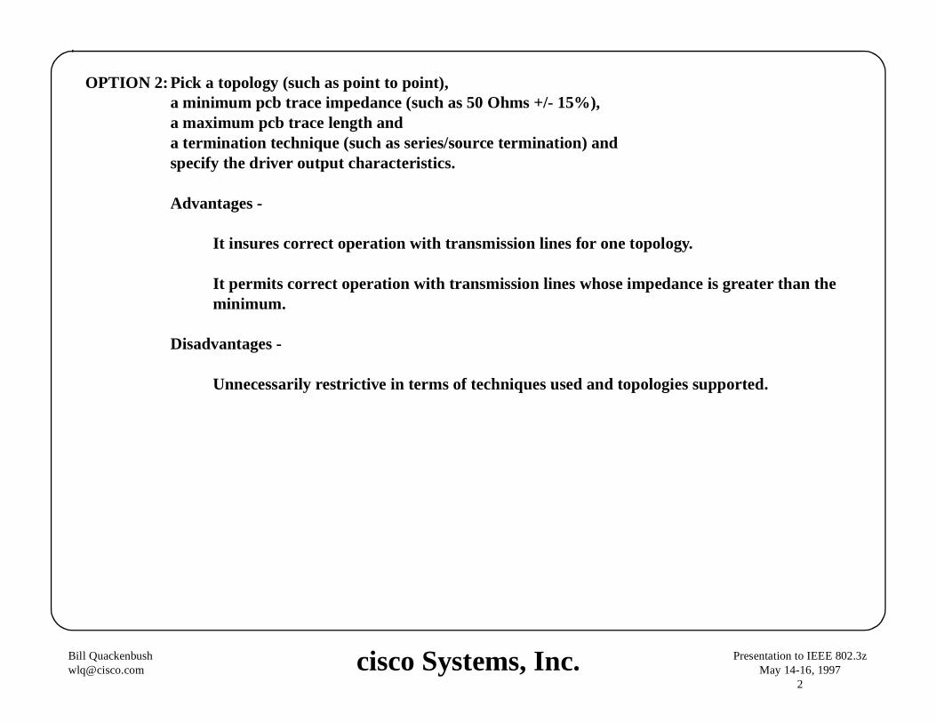
OPTION 2:Pick a topology (such as point to point),a minimum pcb trace impedance (such as 50 Ohms +/- 15%),a maximum pcb trace length anda termination technique (such as series/source termination) andspecify the driver output characteristics.
Advantages -
It insures correct operation with transmission lines for one topology.
It permits correct operation with transmission lines whose impedance is greater than the minimum.
Disadvantages -
Unnecessaril y restrictive in terms of techniques used and topologies supported.
cisco Systems, Inc.Bil l [email protected]
Presentation to IEEE 802.3zMay 14-16, 1997
3
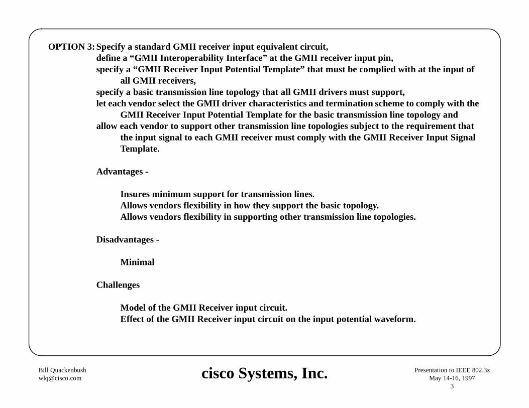
OPTION 3:Specify a standard GMII receiver input equivalent circuit,define a “GMII I nteroperabili ty Interface” at the GMII receiver input pin,specify a “ GMII Receiver Input Potential Template” that must be complied with at the input of
all GMII receivers,specify a basic transmission line topology that all GMII driver s must support,let each vendor select the GMII driver characteristics and termination scheme to comply with the
GMII Receiver Input Potential Template for the basic transmission line topology andallow each vendor to support other transmission line topologies subject to the requirement that
the input signal to each GMII receiver must comply with the GMII Receiver Input Signal Template.
Advantages -
Insures minimum support for transmission lines.All ows vendors flexibil ity in how they support the basic topology.All ows vendors flexibil ity in supporting other transmission line topologies.
Disadvantages -
Minimal
Challenges
Model of the GMII Receiver input circuit.Effect of the GMII Receiver input circuit on the input potential waveform.
cisco Systems, Inc.Bil l [email protected]
Presentation to IEEE 802.3zMay 14-16, 1997
4
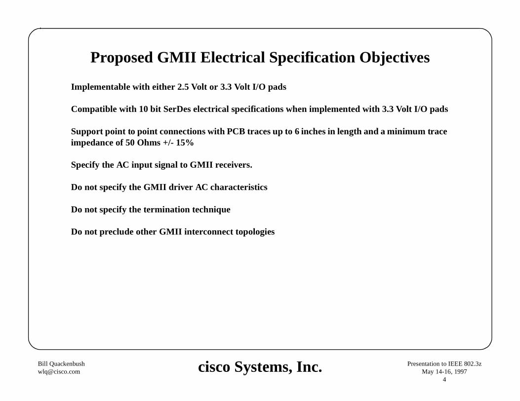
Proposed GMII Electrical Specification Objectives
Implementable with either 2.5 Volt or 3.3 Volt I/O pads
Compatible with 10 bit SerDes electrical specifications when implemented with 3.3 Volt I/O pads
Support point to point connections with PCB traces up to 6 inches in length and a minimum trace impedance of 50 Ohms +/- 15%
Specify the AC input signal to GMII receivers.
Do not specify the GMII driver AC characteristics
Do not specify the termination technique
Do not preclude other GMII interconnect topologies
cisco Systems, Inc.Bil l [email protected]
Presentation to IEEE 802.3zMay 14-16, 1997
5
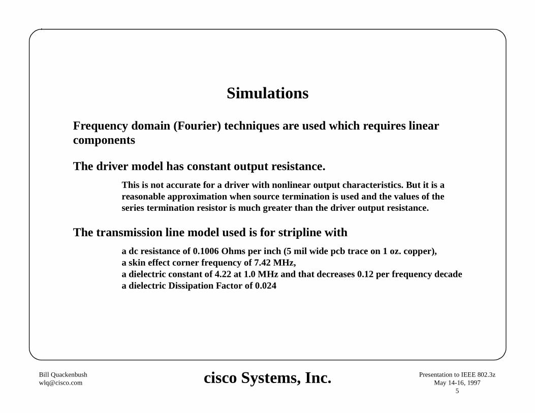
Simulations
Frequency domain (Fourier) techniques are used which requires linear components
The driver model has constant output resistance.
This is not accurate for a driver with nonlinear output characteristics. But it is a reasonable approximation when source termination is used and the values of the series termination resistor is much greater than the driver output resistance.
The transmission line model used is for stripli ne with
a dc resistance of 0.1006 Ohms per inch (5 mil wide pcb trace on 1 oz. copper),a skin effect corner frequency of 7.42 MHz,a dielectric constant of 4.22 at 1.0 MHz and that decreases 0.12 per frequency decadea dielectric Dissipation Factor of 0.024
cisco Systems, Inc.Bil l [email protected]
Presentation to IEEE 802.3zMay 14-16, 1997
6
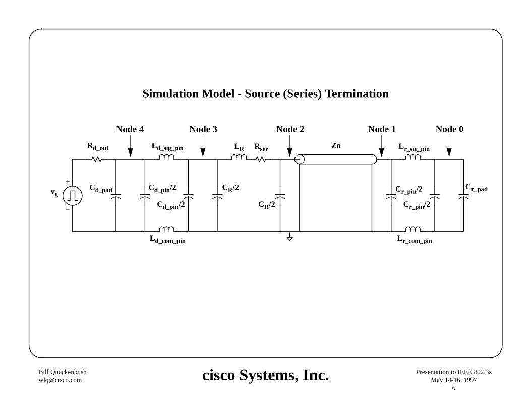
vg
Rd_out
Cd_pad
Ld_sig_pin
Ld_com_pin
Cd_pin/2
RserLR
CR/2 Cr_pin/2
Cr_pad
L r_sig_pin
Lr_com_pin
Zo
+
_
CR/2 Cr_pin/2
Cd_pin/2
Simulation Model - Source (Series) Termination
Node 0Node 1Node 2Node 3Node 4
cisco Systems, Inc.Bil l [email protected]
Presentation to IEEE 802.3zMay 14-16, 1997
7
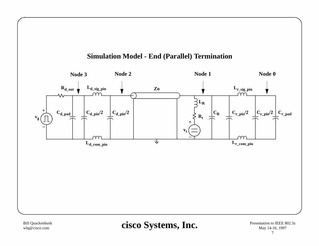
vg
Rd_out
Cd_pad
Ld_sig_pin
Ld_com_pin
Cd_pin/2Rt
LR
CR Cr_pin/2 Cr_pad
L r_sig_pin
Lr_com_pin
Zo
+
_
Cr_pin/2Cd_pin/2
Simulation Model - End (Parallel) Termination
vt
+
_
Node 0Node 1Node 2Node 3
cisco Systems, Inc.Bil l [email protected]
Presentation to IEEE 802.3zMay 14-16, 1997
8
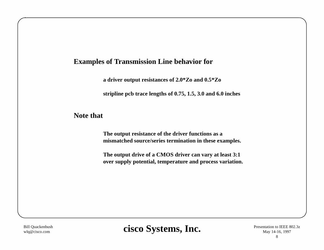
Examples of Transmission Line behavior for
a driver output resistances of 2.0*Zo and 0.5*Zo
stripline pcb trace lengths of 0.75, 1.5, 3.0 and 6.0 inches
Note that
The output resistance of the driver functions as a mismatched source/series termination in these examples.
The output drive of a CMOS driver can vary at least 3:1 over supply potential, temperature and process variation.
cisco Systems, Inc.Bil l [email protected]
Presentation to IEEE 802.3zMay 14-16, 1997
9
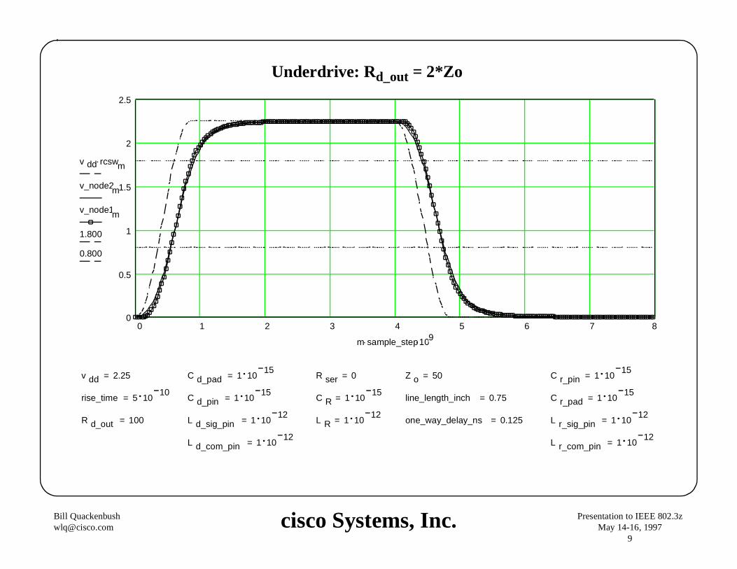
0 1 2 3 4 5 6 7 80
0.5
1
1.5
2
2.5
.v dd rcswm
v_node2m
v_node1m
1.800
0.800
..m sample_step109
=v dd 2.25 =C d_pad 1 1015
=R ser 0 =Z o 50 =C r_pin 1 1015
=rise_time 5 1010
=C d_pin 1 1015
=C R 1 1015
=line_length_inch 0.75 =C r_pad 1 1015
=R d_out 100 =L d_sig_pin 1 1012
=L R 1 1012
=one_way_delay_ns 0.125 =L r_sig_pin 1 1012
=L d_com_pin 1 1012
=L r_com_pin 1 1012
Underdrive: Rd_out = 2*Zo
cisco Systems, Inc.Bil l [email protected]
Presentation to IEEE 802.3zMay 14-16, 1997
10
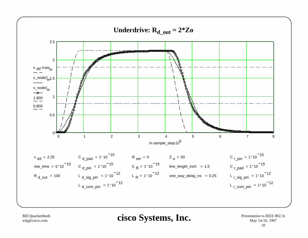
0 1 2 3 4 5 6 7 80
0.5
1
1.5
2
2.5
.v dd rcswm
v_node2m
v_node1m
1.800
0.800
..m sample_step109
=v dd 2.25 =C d_pad 1 1015
=R ser 0 =Z o 50 =C r_pin 1 1015
=rise_time 5 1010
=C d_pin 1 1015
=C R 1 1015
=line_length_inch 1.5 =C r_pad 1 1015
=R d_out 100 =L d_sig_pin 1 1012
=L R 1 1012
=one_way_delay_ns 0.25 =L r_sig_pin 1 1012
=L d_com_pin 1 1012
=L r_com_pin 1 1012
Underdrive: Rd_out = 2*Zo
cisco Systems, Inc.Bil l [email protected]
Presentation to IEEE 802.3zMay 14-16, 1997
11
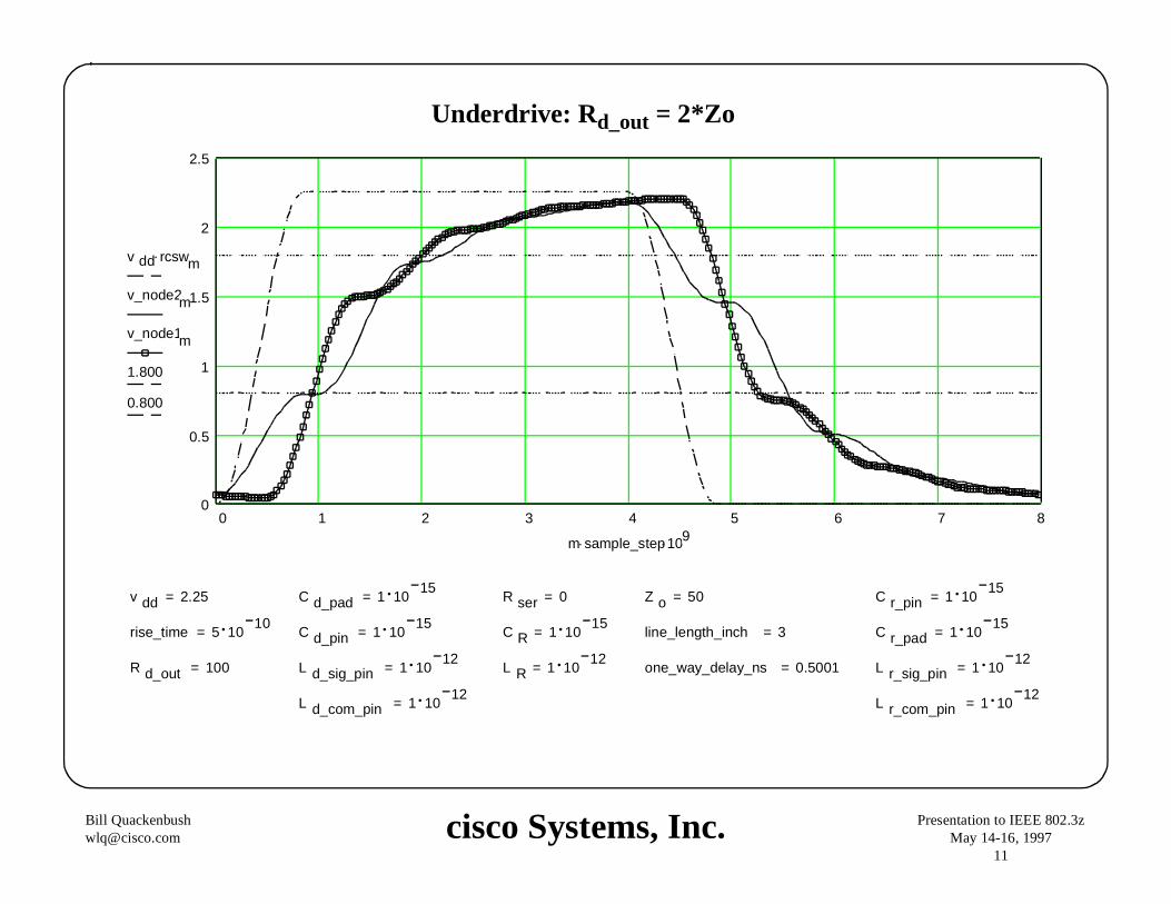
0 1 2 3 4 5 6 7 80
0.5
1
1.5
2
2.5
.v dd rcswm
v_node2m
v_node1m
1.800
0.800
..m sample_step109
=v dd 2.25 =C d_pad 1 1015
=R ser 0 =Z o 50 =C r_pin 1 1015
=rise_time 5 1010
=C d_pin 1 1015
=C R 1 1015
=line_length_inch 3 =C r_pad 1 1015
=R d_out 100 =L d_sig_pin 1 1012
=L R 1 1012
=one_way_delay_ns 0.5001 =L r_sig_pin 1 1012
=L d_com_pin 1 1012
=L r_com_pin 1 1012
Underdrive: Rd_out = 2*Zo
cisco Systems, Inc.Bil l [email protected]
Presentation to IEEE 802.3zMay 14-16, 1997
12
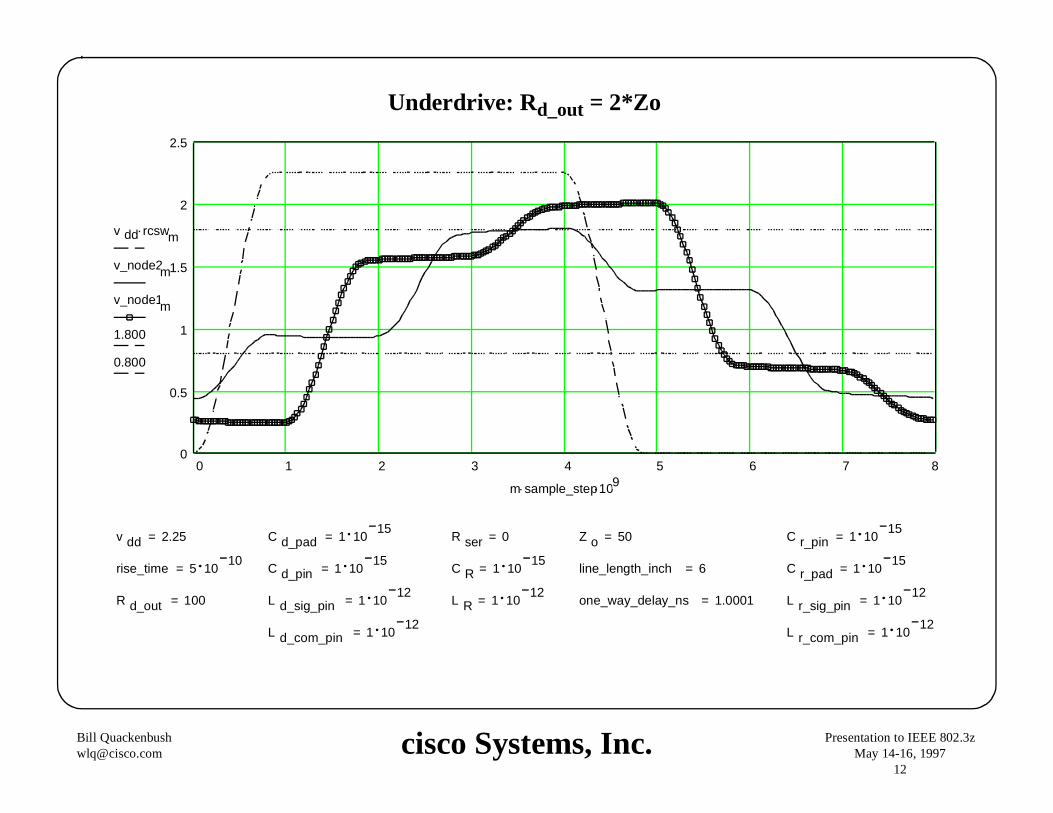
0 1 2 3 4 5 6 7 80
0.5
1
1.5
2
2.5
.v dd rcswm
v_node2m
v_node1m
1.800
0.800
..m sample_step109
=v dd 2.25 =C d_pad 1 1015
=R ser 0 =Z o 50 =C r_pin 1 1015
=rise_time 5 1010
=C d_pin 1 1015
=C R 1 1015
=line_length_inch 6 =C r_pad 1 1015
=R d_out 100 =L d_sig_pin 1 1012
=L R 1 1012
=one_way_delay_ns 1.0001 =L r_sig_pin 1 1012
=L d_com_pin 1 1012
=L r_com_pin 1 1012
Underdrive: Rd_out = 2*Zo
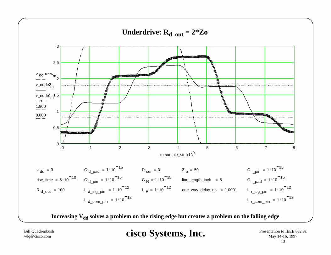
cisco Systems, Inc.Bil l [email protected]
Presentation to IEEE 802.3zMay 14-16, 1997
13
Increasing Vdd solves a problem on the rising edge but creates a problem on the fall ing edge
0 1 2 3 4 5 6 7 80
0.5
1
1.5
2
2.5
3
.v dd rcswm
v_node2m
v_node1m
1.800
0.800
..m sample_step109
=v dd 3 =C d_pad 1 1015
=R ser 0 =Z o 50 =C r_pin 1 1015
=rise_time 5 1010
=C d_pin 1 1015
=C R 1 1015
=line_length_inch 6 =C r_pad 1 1015
=R d_out 100 =L d_sig_pin 1 1012
=L R 1 1012
=one_way_delay_ns 1.0001 =L r_sig_pin 1 1012
=L d_com_pin 1 1012
=L r_com_pin 1 1012
Underdrive: Rd_out = 2*Zo
cisco Systems, Inc.Bil l [email protected]
Presentation to IEEE 802.3zMay 14-16, 1997
14
0 1 2 3 4 5 6 7 80.5
0
0.5
1
1.5
2
2.5
3
.v dd rcswm
v_node2m
v_node1m
1.800
0.800
..m sample_step109
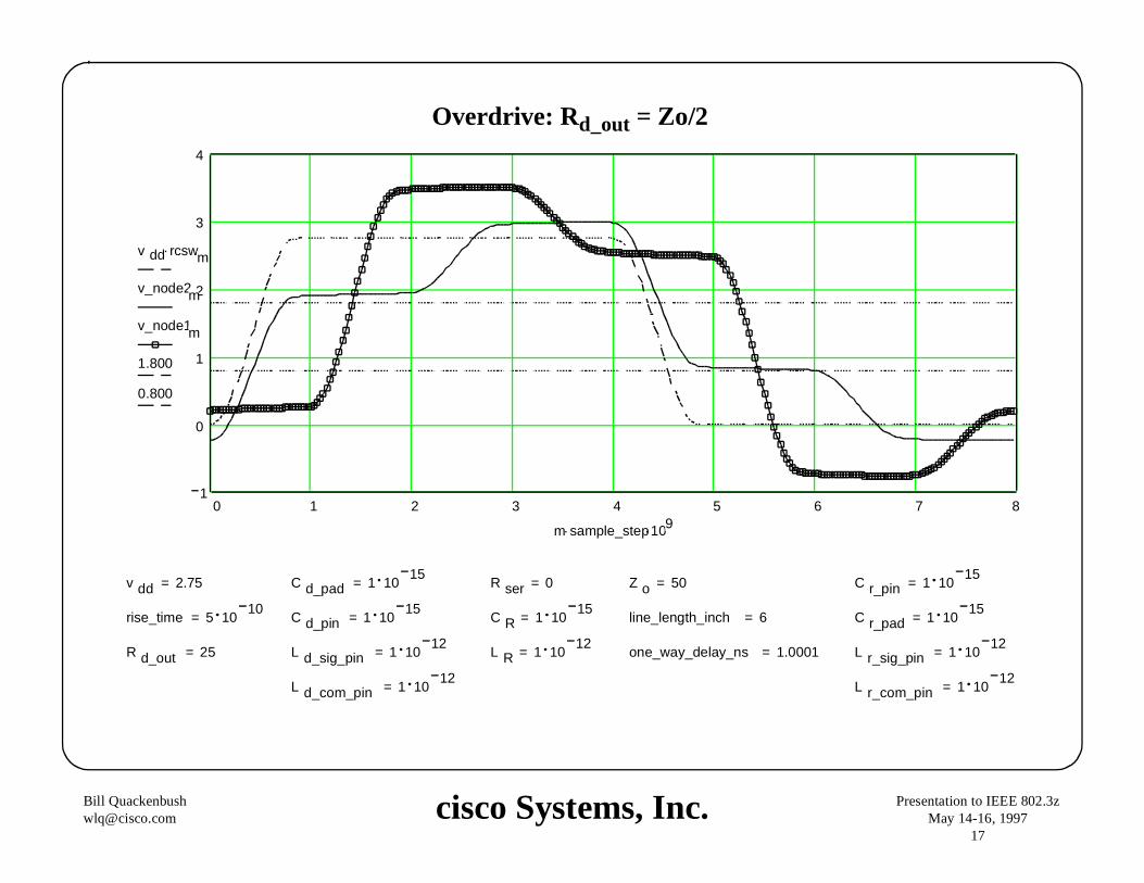
=v dd 2.75 =C d_pad 1 1015
=R ser 0 =Z o 50 =C r_pin 1 1015
=rise_time 5 1010
=C d_pin 1 1015
=C R 1 1015
=line_length_inch 0.75 =C r_pad 1 1015
=R d_out 25 =L d_sig_pin 1 1012
=L R 1 1012
=one_way_delay_ns 0.125 =L r_sig_pin 1 1012
=L d_com_pin 1 1012
=L r_com_pin 1 1012
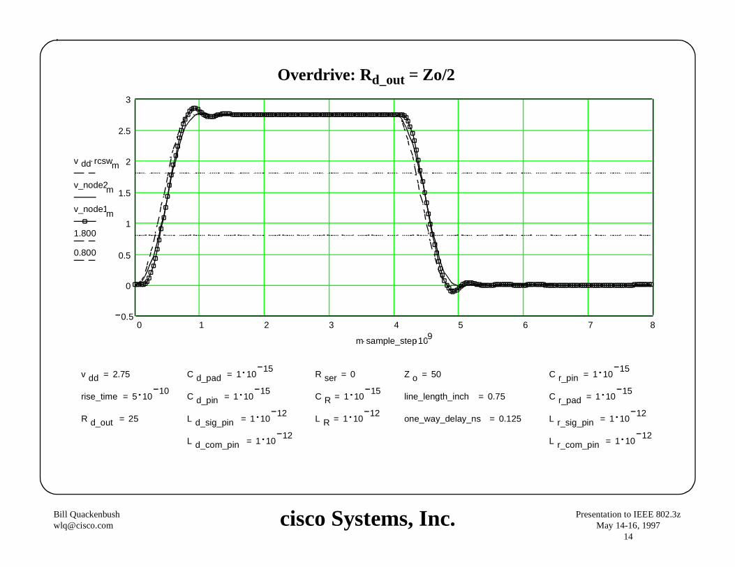
Overdrive: Rd_out = Zo/2
cisco Systems, Inc.Bil l [email protected]
Presentation to IEEE 802.3zMay 14-16, 1997
15
0 1 2 3 4 5 6 7 81
0
1
2
3
4
.v dd rcswm
v_node2m
v_node1m
1.800
0.800
..m sample_step109
=v dd 2.75 =C d_pad 1 1015
=R ser 0 =Z o 50 =C r_pin 1 1015
=rise_time 5 1010
=C d_pin 1 1015
=C R 1 1015
=line_length_inch 1.5 =C r_pad 1 1015
=R d_out 25 =L d_sig_pin 1 1012
=L R 1 1012
=one_way_delay_ns 0.25 =L r_sig_pin 1 1012
=L d_com_pin 1 1012
=L r_com_pin 1 1012
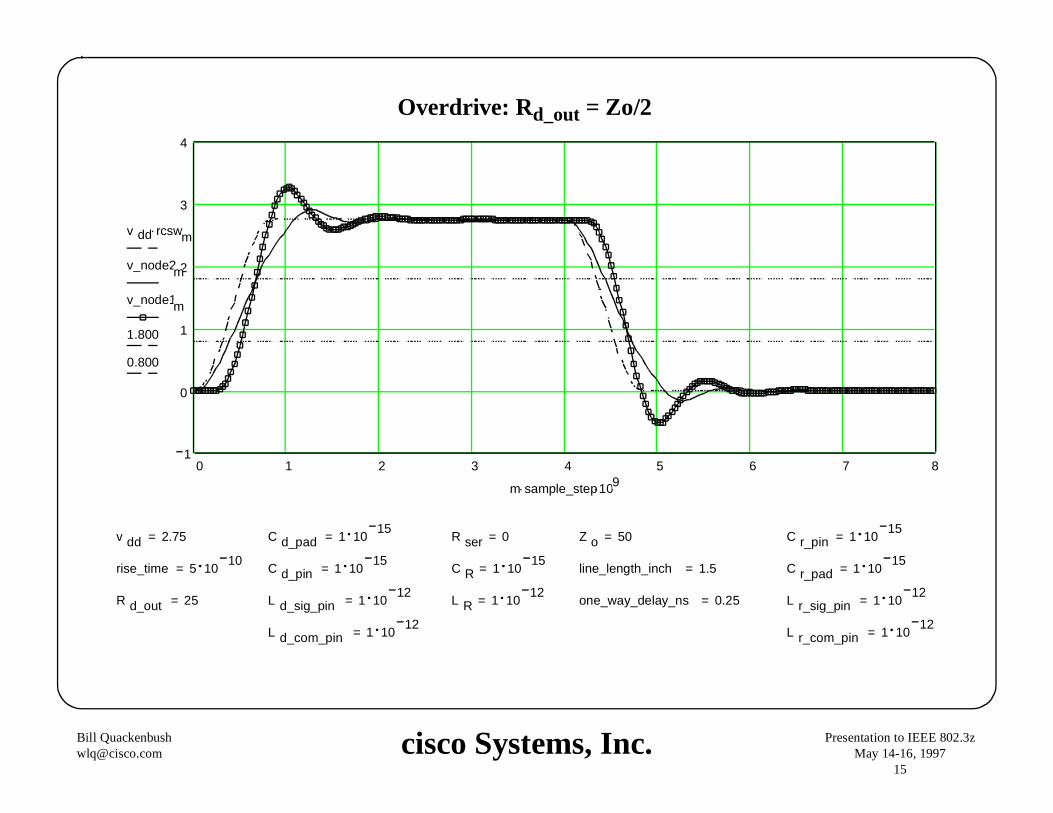
Overdrive: Rd_out = Zo/2
cisco Systems, Inc.Bil l [email protected]
Presentation to IEEE 802.3zMay 14-16, 1997
16
0 1 2 3 4 5 6 7 81
0
1
2
3
4
.v dd rcswm
v_node2m
v_node1m
1.800
0.800
..m sample_step109
=v dd 2.75 =C d_pad 1 1015
=R ser 0 =Z o 50 =C r_pin 1 1015
=rise_time 5 1010
=C d_pin 1 1015
=C R 1 1015
=line_length_inch 3 =C r_pad 1 1015
=R d_out 25 =L d_sig_pin 1 1012
=L R 1 1012
=one_way_delay_ns 0.5001 =L r_sig_pin 1 1012
=L d_com_pin 1 1012
=L r_com_pin 1 1012
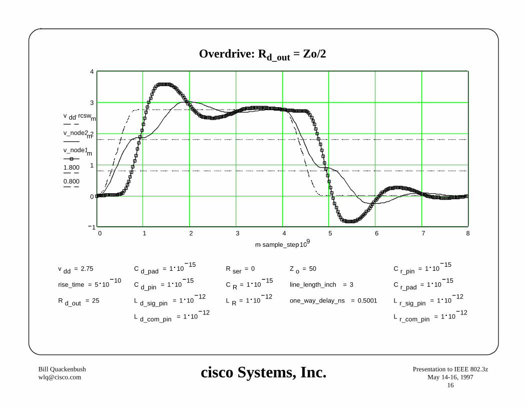
Overdrive: Rd_out = Zo/2
cisco Systems, Inc.Bil l [email protected]
Presentation to IEEE 802.3zMay 14-16, 1997
17
0 1 2 3 4 5 6 7 81
0
1
2
3
4
.v dd rcswm
v_node2m
v_node1m
1.800
0.800
..m sample_step109
=v dd 2.75 =C d_pad 1 1015
=R ser 0 =Z o 50 =C r_pin 1 1015
=rise_time 5 1010
=C d_pin 1 1015
=C R 1 1015
=line_length_inch 6 =C r_pad 1 1015
=R d_out 25 =L d_sig_pin 1 1012
=L R 1 1012
=one_way_delay_ns 1.0001 =L r_sig_pin 1 1012
=L d_com_pin 1 1012
=L r_com_pin 1 1012
Overdrive: Rd_out = Zo/2
cisco Systems, Inc.Bil l [email protected]
Presentation to IEEE 802.3zMay 14-16, 1997
18
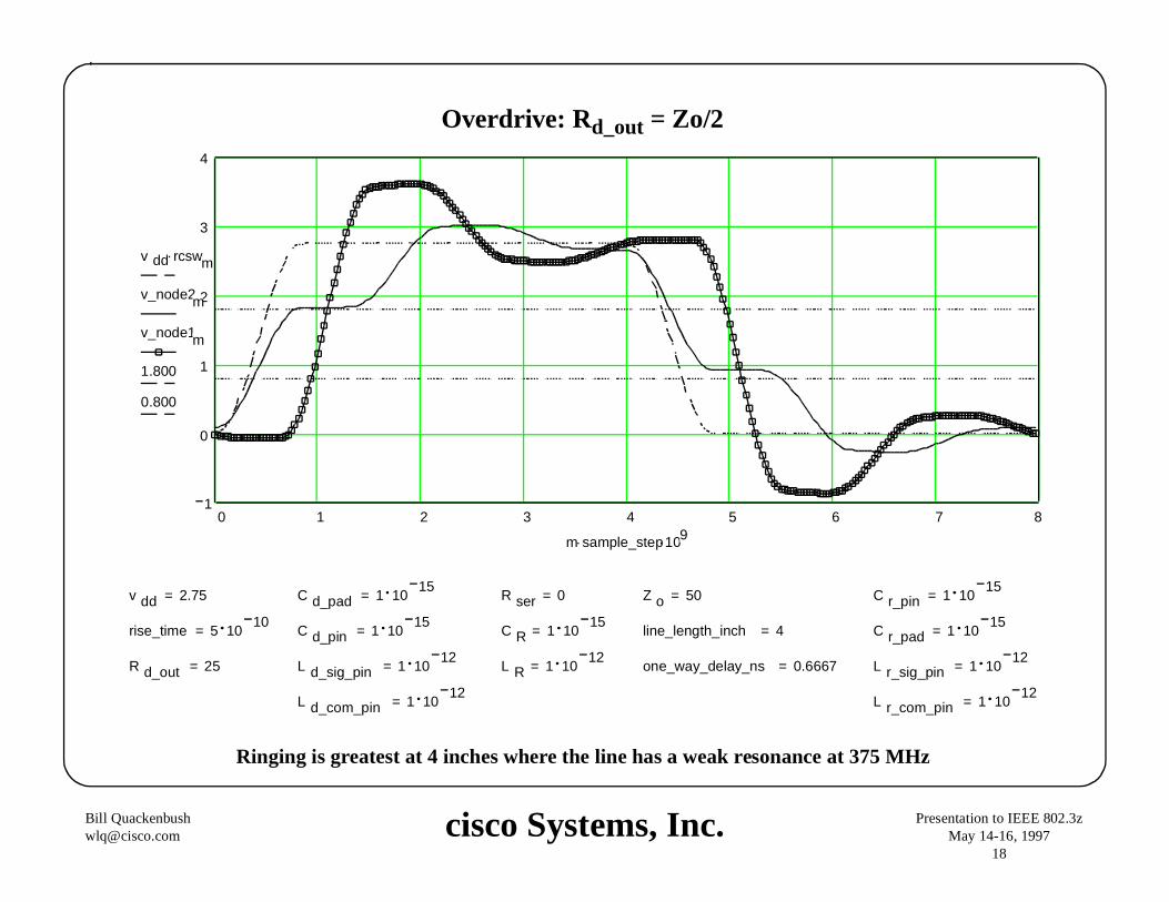
Ringing is greatest at 4 inches where the line has a weak resonance at 375 MHz
0 1 2 3 4 5 6 7 81
0
1
2
3
4
.v dd rcswm
v_node2m
v_node1m
1.800
0.800
..m sample_step109
=v dd 2.75 =C d_pad 1 1015
=R ser 0 =Z o 50 =C r_pin 1 1015
=rise_time 5 1010
=C d_pin 1 1015
=C R 1 1015
=line_length_inch 4 =C r_pad 1 1015
=R d_out 25 =L d_sig_pin 1 1012
=L R 1 1012
=one_way_delay_ns 0.6667 =L r_sig_pin 1 1012
=L d_com_pin 1 1012
=L r_com_pin 1 1012
Overdrive: Rd_out = Zo/2
cisco Systems, Inc.Bil l [email protected]
Presentation to IEEE 802.3zMay 14-16, 1997
19
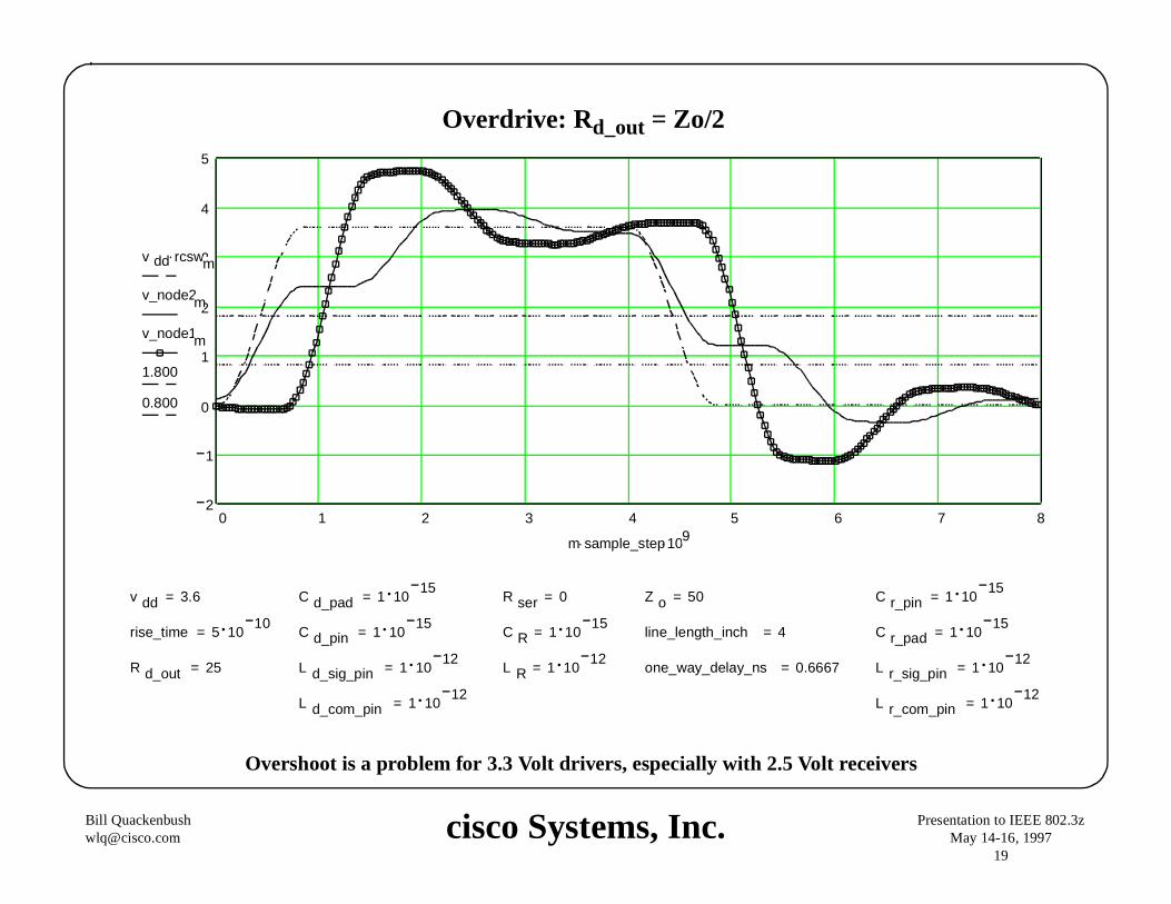
Overshoot is a problem for 3.3 Volt driver s, especially with 2.5 Volt receivers
0 1 2 3 4 5 6 7 82
1
0
1
2
3
4
5
.v dd rcswm
v_node2m
v_node1m
1.800
0.800
..m sample_step109
=v dd 3.6 =C d_pad 1 1015
=R ser 0 =Z o 50 =C r_pin 1 1015
=rise_time 5 1010
=C d_pin 1 1015
=C R 1 1015
=line_length_inch 4 =C r_pad 1 1015
=R d_out 25 =L d_sig_pin 1 1012
=L R 1 1012
=one_way_delay_ns 0.6667 =L r_sig_pin 1 1012
=L d_com_pin 1 1012
=L r_com_pin 1 1012
Overdrive: Rd_out = Zo/2
cisco Systems, Inc.Bil l [email protected]
Presentation to IEEE 802.3zMay 14-16, 1997
20
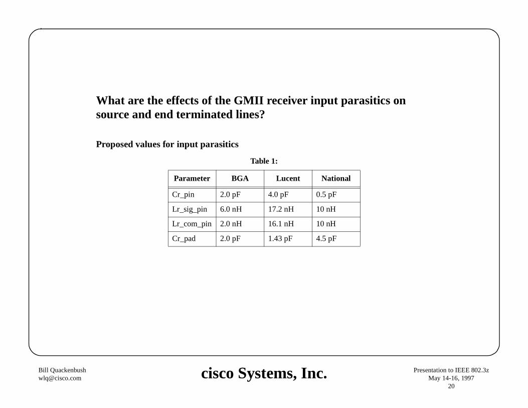
What are the effects of the GMII receiver input parasitics on source and end terminated lines?
Proposed values for input parasitics
Table 1:
Parameter BGA Lucent National
Cr_pin 2.0 pF 4.0 pF 0.5 pF
Lr_sig_pin 6.0 nH 17.2 nH 10 nH
Lr_com_pin 2.0 nH 16.1 nH 10 nH
Cr_pad 2.0 pF 1.43 pF 4.5 pF
cisco Systems, Inc.Bil l [email protected]
Presentation to IEEE 802.3zMay 14-16, 1997
21
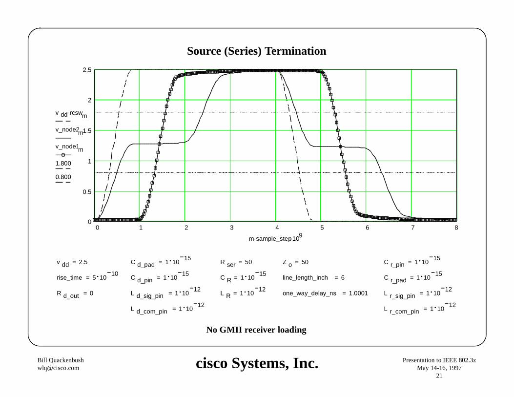
Source (Series) Termination
0 1 2 3 4 5 6 7 80
0.5
1
1.5
2
2.5
.v dd rcswm
v_node2m
v_node1m
1.800
0.800
..m sample_step109
=v dd 2.5 =C d_pad 1 1015
=R ser 50 =Z o 50 =C r_pin 1 1015
=rise_time 5 1010
=C d_pin 1 1015
=C R 1 1015
=line_length_inch 6 =C r_pad 1 1015
=R d_out 0 =L d_sig_pin 1 1012
=L R 1 1012
=one_way_delay_ns 1.0001 =L r_sig_pin 1 1012
=L d_com_pin 1 1012
=L r_com_pin 1 1012
No GMII receiver loading
cisco Systems, Inc.Bil l [email protected]
Presentation to IEEE 802.3zMay 14-16, 1997
22
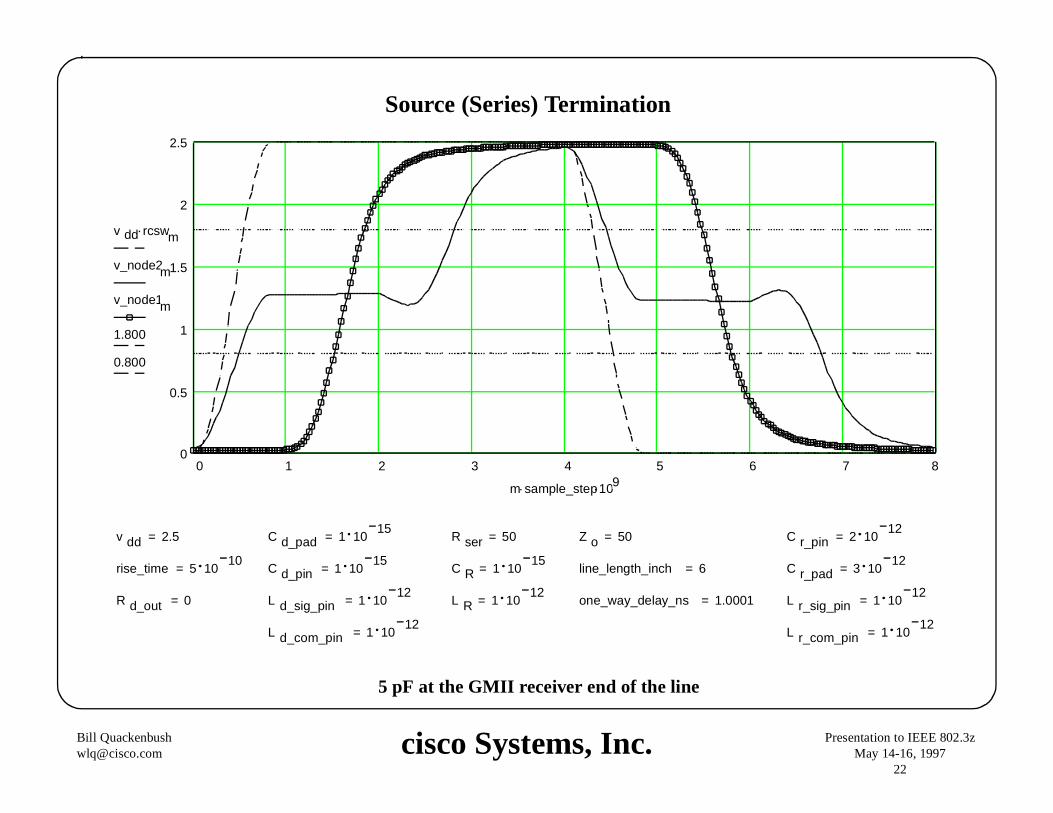
Source (Series) Termination
5 pF at the GMII receiver end of the line
0 1 2 3 4 5 6 7 80
0.5
1
1.5
2
2.5
.v dd rcswm
v_node2m
v_node1m
1.800
0.800
..m sample_step109
=v dd 2.5 =C d_pad 1 1015
=R ser 50 =Z o 50 =C r_pin 2 1012
=rise_time 5 1010
=C d_pin 1 1015
=C R 1 1015
=line_length_inch 6 =C r_pad 3 1012
=R d_out 0 =L d_sig_pin 1 1012
=L R 1 1012
=one_way_delay_ns 1.0001 =L r_sig_pin 1 1012
=L d_com_pin 1 1012
=L r_com_pin 1 1012
cisco Systems, Inc.Bil l [email protected]
Presentation to IEEE 802.3zMay 14-16, 1997
23
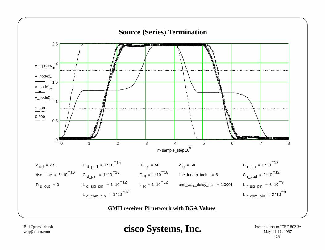
Source (Series) Termination
GMII receiver Pi network with BGA Values
0 1 2 3 4 5 6 7 80
0.5
1
1.5
2
2.5
.v dd rcswm
v_node2m
v_node1m
v_node0m
1.800
0.800
..m sample_step109
=v dd 2.5 =C d_pad 1 1015
=R ser 50 =Z o 50 =C r_pin 2 1012
=rise_time 5 1010
=C d_pin 1 1015
=C R 1 1015
=line_length_inch 6 =C r_pad 2 1012
=R d_out 0 =L d_sig_pin 1 1012
=L R 1 1012
=one_way_delay_ns 1.0001 =L r_sig_pin 6 109
=L d_com_pin 1 1012
=L r_com_pin 2 109

cisco Systems, Inc.Bil l [email protected]
Presentation to IEEE 802.3zMay 14-16, 1997
24
Source (Series) Termination
GMII receiver Pi network with Lucent Values
0 1 2 3 4 5 6 7 81
0
1
2
3
4
.v dd rcswm
v_node2m
v_node1m
v_node0m
1.800
0.800
..m sample_step109
=v dd 2.5 =C d_pad 1 1015
=R ser 50 =Z o 50 =C r_pin 4 1012
=rise_time 5 1010
=C d_pin 1 1015
=C R 1 1015
=line_length_inch 6 =C r_pad 1.43 1012
=R d_out 0 =L d_sig_pin 1 1012
=L R 1 1012
=one_way_delay_ns 1.0001 =L r_sig_pin 1.72 108
=L d_com_pin 1 1012
=L r_com_pin 1.61 108
cisco Systems, Inc.Bil l [email protected]
Presentation to IEEE 802.3zMay 14-16, 1997
25
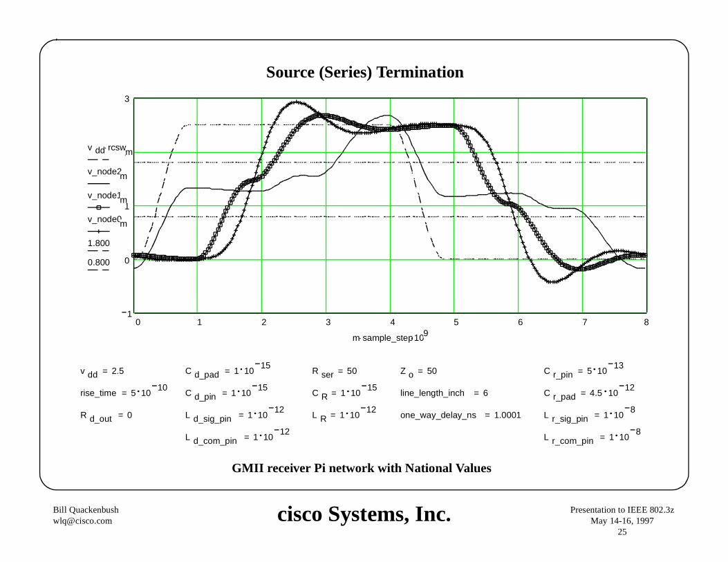
Source (Series) Termination
0 1 2 3 4 5 6 7 81
0
1
2
3
.v dd rcswm
v_node2m
v_node1m
v_node0m
1.800
0.800
..m sample_step109
=v dd 2.5 =C d_pad 1 1015
=R ser 50 =Z o 50 =C r_pin 5 1013
=rise_time 5 1010
=C d_pin 1 1015
=C R 1 1015
=line_length_inch 6 =C r_pad 4.5 1012
=R d_out 0 =L d_sig_pin 1 1012
=L R 1 1012
=one_way_delay_ns 1.0001 =L r_sig_pin 1 108
=L d_com_pin 1 1012
=L r_com_pin 1 108
GMII receiver Pi network with National Values
cisco Systems, Inc.Bil l [email protected]
Presentation to IEEE 802.3zMay 14-16, 1997
26
Source (Series) Termination
0 1 2 3 4 5 6 7 80.5
0
0.5
1
1.5
2
2.5
3
.v dd rcswm
v_node2m
v_node1m
v_node0m
1.800
0.800
..m sample_step109
=v dd 2.5 =C d_pad 1 1015
=R ser 100 =Z o 100 =C r_pin 4 1012
=rise_time 5 1010
=C d_pin 1 1015
=C R 1 1015
=line_length_inch 6 =C r_pad 1.43 1012
=R d_out 0 =L d_sig_pin 1 1012
=L R 1 1012
=one_way_delay_ns 1.0002 =L r_sig_pin 1.72 108
=L d_com_pin 1 1012
=L r_com_pin 1.61 108
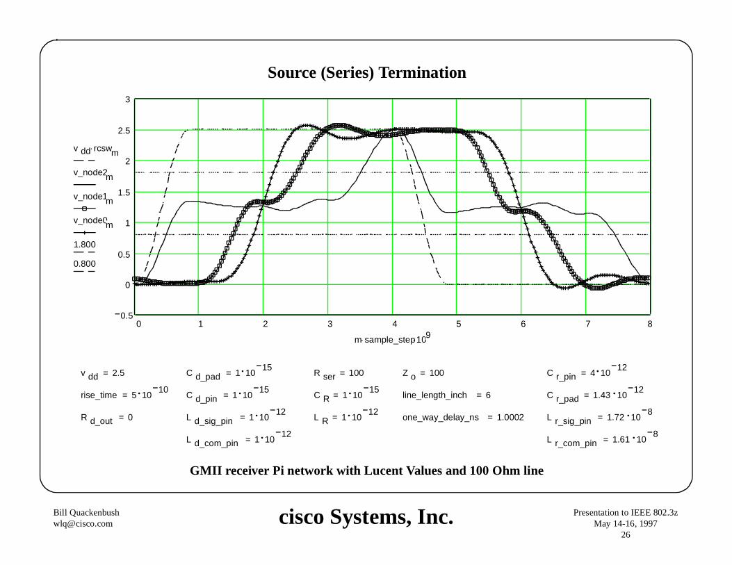
GMII receiver Pi network with Lucent Values and 100 Ohm line
cisco Systems, Inc.Bil l [email protected]
Presentation to IEEE 802.3zMay 14-16, 1997
27
0 1 2 3 4 5 6 7 80.5
0
0.5
1
1.5
2
2.5
3
.v dd rcswm
v_node2m
v_node1m
v_node0m
1.800
0.800
..m sample_step109
=v dd 2.5 =C d_pad 1 1015
=R ser 50 =Z o 50 =C r_pin 4 1012
=rise_time 1 109
=C d_pin 1 1015
=C R 1 1015
=line_length_inch 6 =C r_pad 1.43 1012
=R d_out 0 =L d_sig_pin 1 1012
=L R 1 1012
=one_way_delay_ns 1.0001 =L r_sig_pin 1.72 108
=L d_com_pin 1 1012
=L r_com_pin 1.61 108
Source (Series) Termination
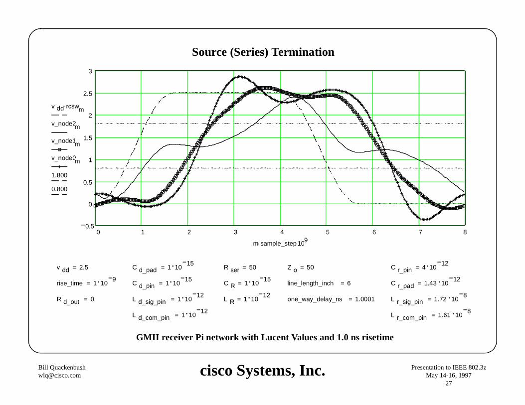
GMII receiver Pi network with Lucent Values and 1.0 ns risetime
cisco Systems, Inc.Bil l [email protected]
Presentation to IEEE 802.3zMay 14-16, 1997
28
End (Parallel) Termination
0 1 2 3 4 5 6 7 80.5
0
0.5
1
1.5
2
2.5
3
.v dd rcswm
v_node2m
v_node1m
1.800
0.800
..m sample_step109
=v dd 2.5 =C d_pad 1 1015
=Z o 50 =R t 50 =C r_pin 1 1015
=rise_time 5 1010
=C d_pin 1 1015
=line_length_inch 6 =C R 1 1015
=C r_pad 1 1015
=R d_out 0 =L d_sig_pin 1 1012
=one_way_delay_ns 1.0001 =L R 1 1012
=L r_sig_pin 1 1012
=L d_com_pin 1 1012
=v t 1.25 =L r_com_pin 1 1012
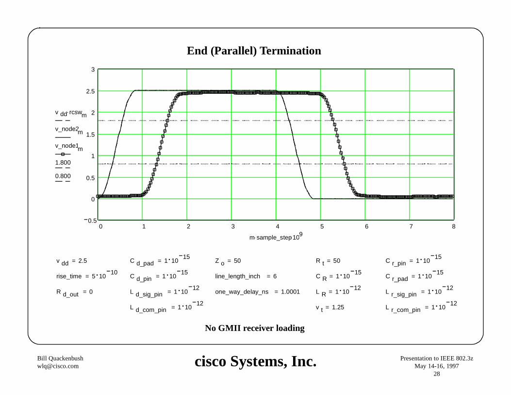
No GMII receiver loading
cisco Systems, Inc.Bil l [email protected]
Presentation to IEEE 802.3zMay 14-16, 1997
29
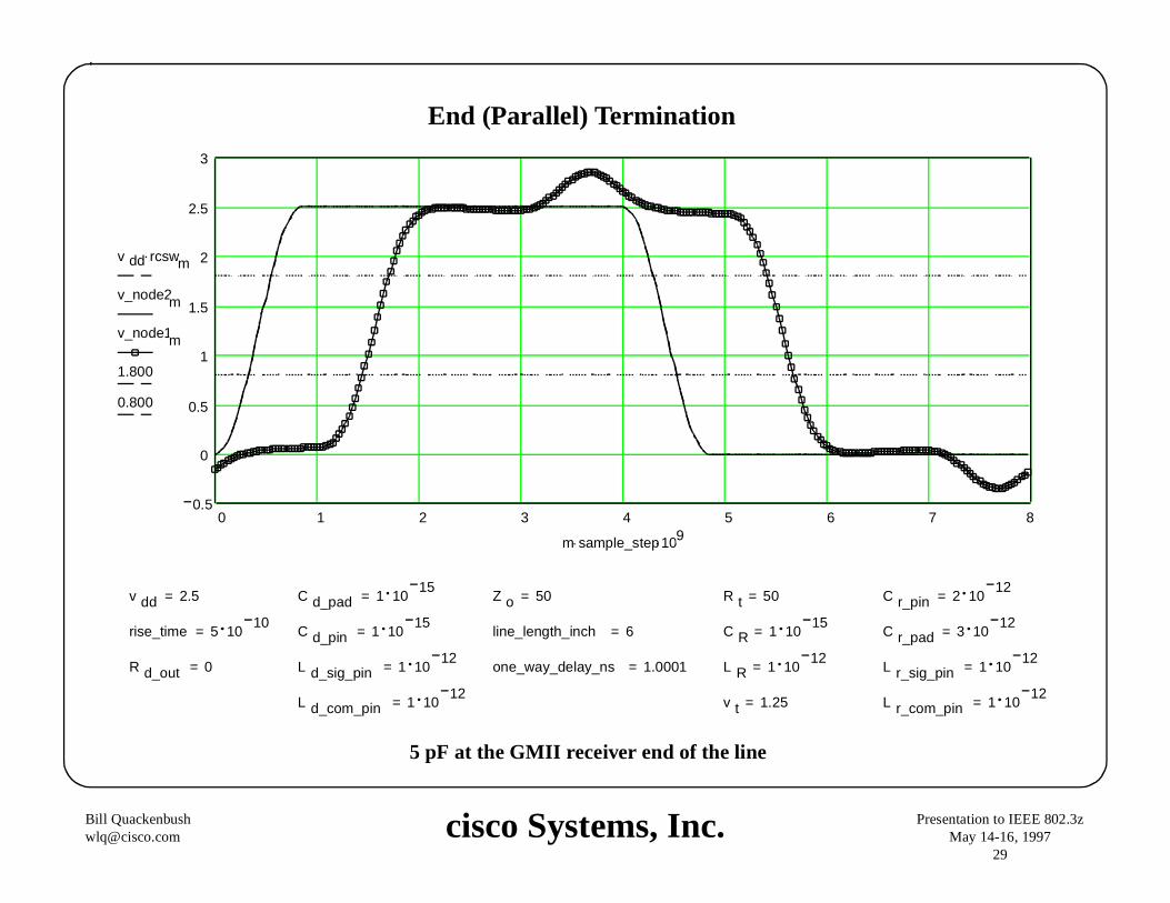
5 pF at the GMII receiver end of the line
End (Parallel) Termination
0 1 2 3 4 5 6 7 80.5
0
0.5
1
1.5
2
2.5
3
.v dd rcswm
v_node2m
v_node1m
1.800
0.800
..m sample_step109
=v dd 2.5 =C d_pad 1 1015
=Z o 50 =R t 50 =C r_pin 2 1012
=rise_time 5 1010
=C d_pin 1 1015
=line_length_inch 6 =C R 1 1015
=C r_pad 3 1012
=R d_out 0 =L d_sig_pin 1 1012
=one_way_delay_ns 1.0001 =L R 1 1012
=L r_sig_pin 1 1012
=L d_com_pin 1 1012
=v t 1.25 =L r_com_pin 1 1012
cisco Systems, Inc.Bil l [email protected]
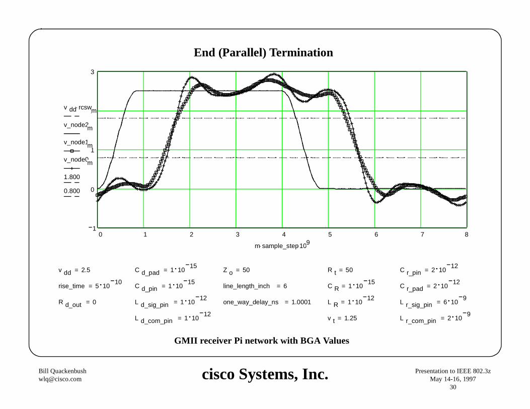
Presentation to IEEE 802.3zMay 14-16, 1997
30
0 1 2 3 4 5 6 7 81
0
1
2
3
.v dd rcswm
v_node2m
v_node1m
v_node0m
1.800
0.800
..m sample_step109
=v dd 2.5 =C d_pad 1 1015
=Z o 50 =R t 50 =C r_pin 2 1012
=rise_time 5 1010
=C d_pin 1 1015
=line_length_inch 6 =C R 1 1015
=C r_pad 2 1012
=R d_out 0 =L d_sig_pin 1 1012
=one_way_delay_ns 1.0001 =L R 1 1012
=L r_sig_pin 6 109
=L d_com_pin 1 1012
=v t 1.25 =L r_com_pin 2 109
End (Parallel) Termination
GMII receiver Pi network with BGA Values
cisco Systems, Inc.Bil l [email protected]
Presentation to IEEE 802.3zMay 14-16, 1997
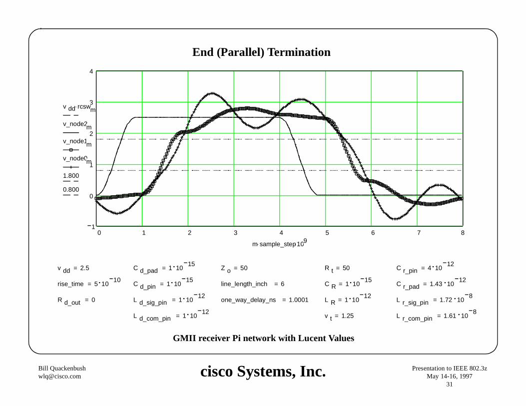
31
0 1 2 3 4 5 6 7 81
0
1
2
3
4
.v dd rcswm
v_node2m
v_node1m
v_node0m
1.800
0.800
..m sample_step109
=v dd 2.5 =C d_pad 1 1015
=Z o 50 =R t 50 =C r_pin 4 1012
=rise_time 5 1010
=C d_pin 1 1015
=line_length_inch 6 =C R 1 1015
=C r_pad 1.43 1012
=R d_out 0 =L d_sig_pin 1 1012
=one_way_delay_ns 1.0001 =L R 1 1012
=L r_sig_pin 1.72 108
=L d_com_pin 1 1012
=v t 1.25 =L r_com_pin 1.61 108
End (Parallel) Termination
GMII receiver Pi network with Lucent Values
cisco Systems, Inc.Bil l [email protected]
Presentation to IEEE 802.3zMay 14-16, 1997
32
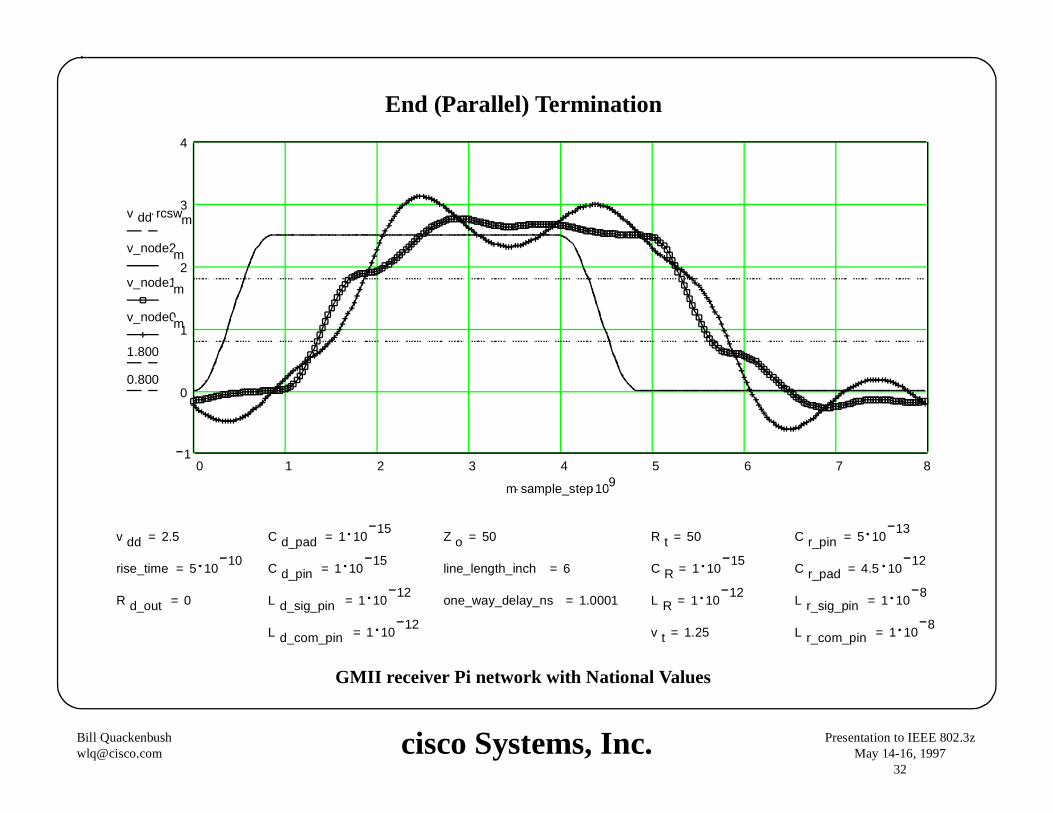
0 1 2 3 4 5 6 7 81
0
1
2
3
4
.v dd rcswm
v_node2m
v_node1m
v_node0m
1.800
0.800
..m sample_step109
=v dd 2.5 =C d_pad 1 1015
=Z o 50 =R t 50 =C r_pin 5 1013
=rise_time 5 1010
=C d_pin 1 1015
=line_length_inch 6 =C R 1 1015
=C r_pad 4.5 1012
=R d_out 0 =L d_sig_pin 1 1012
=one_way_delay_ns 1.0001 =L R 1 1012
=L r_sig_pin 1 108
=L d_com_pin 1 1012
=v t 1.25 =L r_com_pin 1 108
End (Parallel) Termination
GMII receiver Pi network with National Values
cisco Systems, Inc.Bil l [email protected]
Presentation to IEEE 802.3zMay 14-16, 1997
33
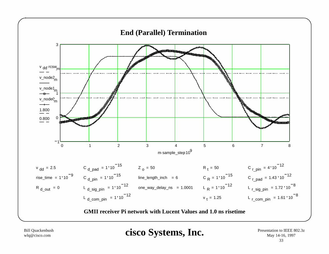
0 1 2 3 4 5 6 7 81
0
1
2
3
.v dd rcswm
v_node2m
v_node1m
v_node0m
1.800
0.800
..m sample_step109
=v dd 2.5 =C d_pad 1 1015
=Z o 50 =R t 50 =C r_pin 4 1012
=rise_time 1 109
=C d_pin 1 1015
=line_length_inch 6 =C R 1 1015
=C r_pad 1.43 1012
=R d_out 0 =L d_sig_pin 1 1012
=one_way_delay_ns 1.0001 =L R 1 1012
=L r_sig_pin 1.72 108
=L d_com_pin 1 1012
=v t 1.25 =L r_com_pin 1.61 108
End (Parallel) Termination
GMII receiver Pi network with Lucent Values and 1.0 ns risetime
cisco Systems, Inc.Bil l [email protected]
Presentation to IEEE 802.3zMay 14-16, 1997
34
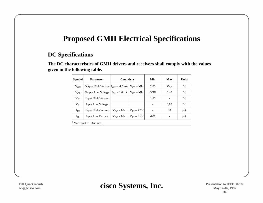
Proposed GMII Electrical Specifications
DC Specifications
The DC characteristics of GMII driver s and receivers shall comply with the values given in the following table.
Symbol Parameter Conditions Min Max Units
VOH Output High Voltage IOH = -1.0mA VCC = Min 2.00 VCC V
VOL Output Low Voltage IOL = 1.0mA VCC = Min GND 0.40 V
VIH Input High Voltage 1,60 - V
VIL Input Low Voltage - 0,80 V
IIH Input High Current VCC = Max VIN = 2.0V - 40 µA
IIL Input Low Current VCC = Max VIN = 0.4V -600 - µA
1 Vcc equal to 3.6V max.
cisco Systems, Inc.Bil l [email protected]
Presentation to IEEE 802.3zMay 14-16, 1997
35
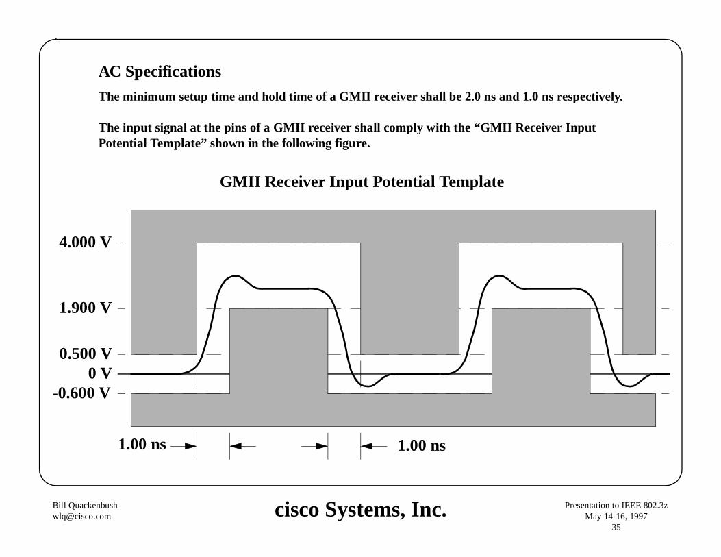
AC Specifications
The minimum setup time and hold time of a GMII receiver shall be 2.0 ns and 1.0 ns respectively.
The input signal at the pins of a GMII receiver shall comply with the “GMII Receiver Input Potential Template” shown in the following figure.
GMII Receiver Input Potential Template
4.000 V
1.900 V
0.500 V0 V
-0.600 V
1.00 ns1.00 ns
cisco Systems, Inc.Bil l [email protected]
Presentation to IEEE 802.3zMay 14-16, 1997
36
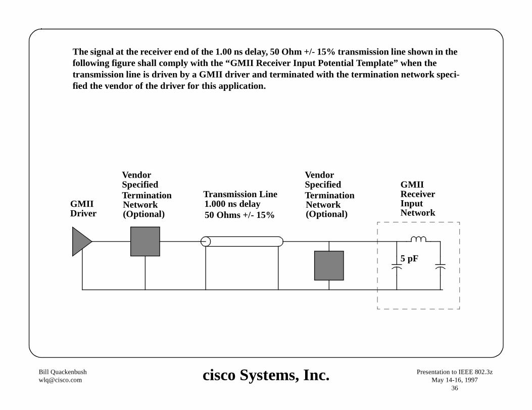
The signal at the receiver end of the 1.00 ns delay, 50 Ohm +/- 15% transmission line shown in the following figure shall comply with the “GMII Receiver Input Potential Template” when the transmission line is driven by a GMII driver and terminated with the termination network speci-fied the vendor of the driver for this application.
Vendor
Termination1.000 ns delay50 Ohms +/- 15%
GMII
Specified
Network
Vendor
TerminationSpecified
NetworkTransmission Line
(Optional) (Optional)
5 pF
Driver
GMIIReceiverInputNetwork