gls55lc200 nand controller (compactflash interface)
TRANSCRIPT
Fact Sheet 01.000 February 2012
These specifications are subject to change without notice. 02/01/2012 © 2012 Greenliant Systems 1 S71365-F
GLS55LC200 NAND Controller (CompactFlash Interface)
Features Supports CompactFlash Revision 3.0 Standard
Interface - Host Interface: 16-bit access - Supports up to PIO Mode-6 - Supports up to Multi-word DMA Mode-4 - Supports up to Ultra DMA Mode-4
Interface for Standard NAND Flash Media - Flash Media Interface: Single or Dual 8-bit
access - Supports up to 4 flash media devices per channel - Supports up to 8 flash media devices directly
- Supports Single-Level Cell (SLC) or Multi-Level Cell (MLC) flash media -2 KByte and 4 KByte program page size
3.3V Power Supply and NAND Flash Interface 5.0V or 3.3V Host Interface Through VDDQ Pins Low Current Operation
- Active mode: 25 mA/35 mA (3.3V/5.0V) (typical)
- Sleep mode: 80 µA/100 µA (3.3V/5.0V) (typical)
Power Management Unit - Immediate disabling of unused circuitry
without host intervention - Zero wake-up latency
20-Byte Unique ID for Enhanced Security - Factory pre-programmed 10-Byte unique ID - User-programmable 10-Byte ID
Programmable, Multitasking NAND Interface Firmware Storage in Embedded SuperFlash®
Pre-programmed Embedded Firmware - Performs self-initialization on first system
Power-on - Executes industry-standard CompactFlash
commands - Implements advanced wear-leveling
algorithms to substantially increase the longevity of flash media
- Embedded Flash File System Built-in Hardware ECC
- Corrects up to 8 random single-bit errors per 512-byte sector
Built-in Internal System Clock Multi-tasking Technology Enables Fast Sustained
Write Performance (Host to Flash) - Supports up to 30 MByte/sec
Fast Sustained Read Performance (Flash to Host) - Up to 30 MByte/sec
Automatic Recognition and Initialization of Flash Media Devices - Seamless integration into a standard SMT
manufacturing process - 5 sec. (typical) for flash drive recognition and
setup Commercial and Industrial Temperature Ranges
- 0°C to 70°C for commercial operation - -40°C to +85°C for industrial operation
Packages Available - 100-lead TQFP – 14mm x 14mm
All Devices are RoHS Compliant
Product Description
The GLS55LC200 NAND Controller is the core of a high-performance, flash media-based, data storage system. The controller recognizes the control, address and data signals on the CF bus and translates them into memory accesses for standard NAND-type flash media. Using both Single Level Cell (SLC) and Multi-Level Cell (MLC) flash media, this technology supports solid state mass storage applications by offering new, expanded functionality while enabling smaller, lighter designs with lower power consumption.
The NAND Controller supports standard CF protocols with up to PIO Mode-6, Multi-word DMA Mode-4, and Ultra DMA Mode-4 interface. The CF interface is widely used in products such as portable and desktop computers, digital cameras, music players, handheld data collection scanners, PDAs, handy terminals, personal communicators, audio recorders, monitoring devices and set-top boxes.
The NAND Controller uses SuperFlash® memory technology, and is factory pre-programmed with an embedded flash file system. Upon initial power-on, the GLS55LC200 recognizes the flash media devices, sets up a bad block table, executes all the necessary handshaking routines for flash media support, and, finally, performs the low-level format. This process typically takes about 3 second plus 0.5 seconds per GByte of drive capacity, allowing a 4 GByte flash drive to be fully initialized in about 5 seconds. For added manufacturing flexibility, system debug, re-initialization and user customization can be accomplished through the CF interface.
The GLS55LC200 high-performance NAND Controller offers sustained read and write performance up to 30MByte/sec. The GLS55LC200 directly supports up to eight flash media devices with appropriate output loading and frequency.
Fact Sheet 01.000 February 2012
These specifications are subject to change without notice. 02/01/2012 © 2012 Greenliant Systems 2 S71365-F
GLS55LC200 NAND Controller (CompactFlash Interface)
The NAND Controller comes pre-programmed with a 10-byte unique serial ID. For even greater system security, the user has the option of programming an additional 10 Bytes of ID space to create a unique, 20-byte ID.
The NAND controller comes packaged in an industry-standard 100-lead TQFP package for easy integration into an SMT manufacturing process.

Fact Sheet 01.000 February 2012
These specifications are subject to change without notice. 02/01/2012 © 2012 Greenliant Systems 3 S71365-F
GLS55LC200 NAND Controller (CompactFlash Interface)
GENERAL DESCRIPTION
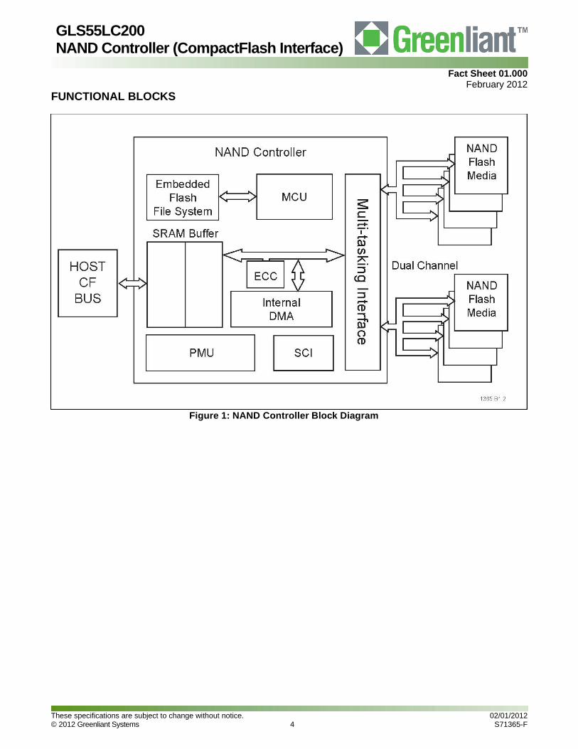
The NAND Controller contains a microcontroller and embedded flash file system integrated in a TQFP package. Refer to Figure 1 for the NAND Controller block diagram. The controller interfaces with the host system allowing data to be written to and read from the flash media.
Performance-optimized NAND Controller
The NAND Controller translates standard CF signals into flash media data and control signals. The following components contribute to the controller’s operation.
Microcontroller Unit (MCU)
The MCU coordinates all related components to complete requested operations.
Internal Direct Memory Access (DMA)
The NAND Controller uses internal DMA which allows instant data transfer from buffer to flash media. This increases the data transfer rate by eliminating the microcontroller overhead associated with the traditional, firmware-based approach.
Power Management Unit (PMU)
The power management unit controls the power consumption of the NAND Controller. It reduces the power consumption of the NAND Controller by putting circuitry not in operation into sleep mode. The PMU has zero wake-up latency.
SRAM Buffer
The NAND Controller performs as an SRAM buffer to optimize the host’s data transfer to and from the flash media.
Embedded Flash File System
The embedded flash file system is an integral part of the NAND Controller. It contains MCU firmware that performs the following tasks:
1. Translates host side signals into flash media writes and reads
2. Provides flash media wear leveling to spread the flash writes across all memory address space to increase the longevity of flash media
3. Keeps track of data file structures
Error Correction Code (ECC)
The NAND Controller uses BCH Error Detection Code (EDC) and Error Correction Code (ECC) algorithms which correct up to eight random single-bit errors for each 512-byte block of data.
High performance is achieved through hardware-based error detection and correction.
Serial Communication Interface (SCI)
The Serial Communication Interface (SCI) is designed to provide trace information during debugging process. To aid in validation, always provide the SCI access to PCB design.
Programmable, Multi-tasking NAND Interface
The multi-tasking interface enables fast, sustained write and read performance by allowing multiple Read, Program and Erase operations to multiple flash media devices. The programmable NAND interface enables timely support of fast changing NAND technology.
Fact Sheet 01.000 February 2012
These specifications are subject to change without notice. 02/01/2012 © 2012 Greenliant Systems 4 S71365-F
GLS55LC200 NAND Controller (CompactFlash Interface)
FUNCTIONAL BLOCKS
Figure 1: NAND Controller Block Diagram
Fact Sheet 01.000 February 2012
These specifications are subject to change without notice. 02/01/2012 © 2012 Greenliant Systems 5 S71365-F
GLS55LC200 NAND Controller (CompactFlash Interface)
PIN ASSIGNMENTS
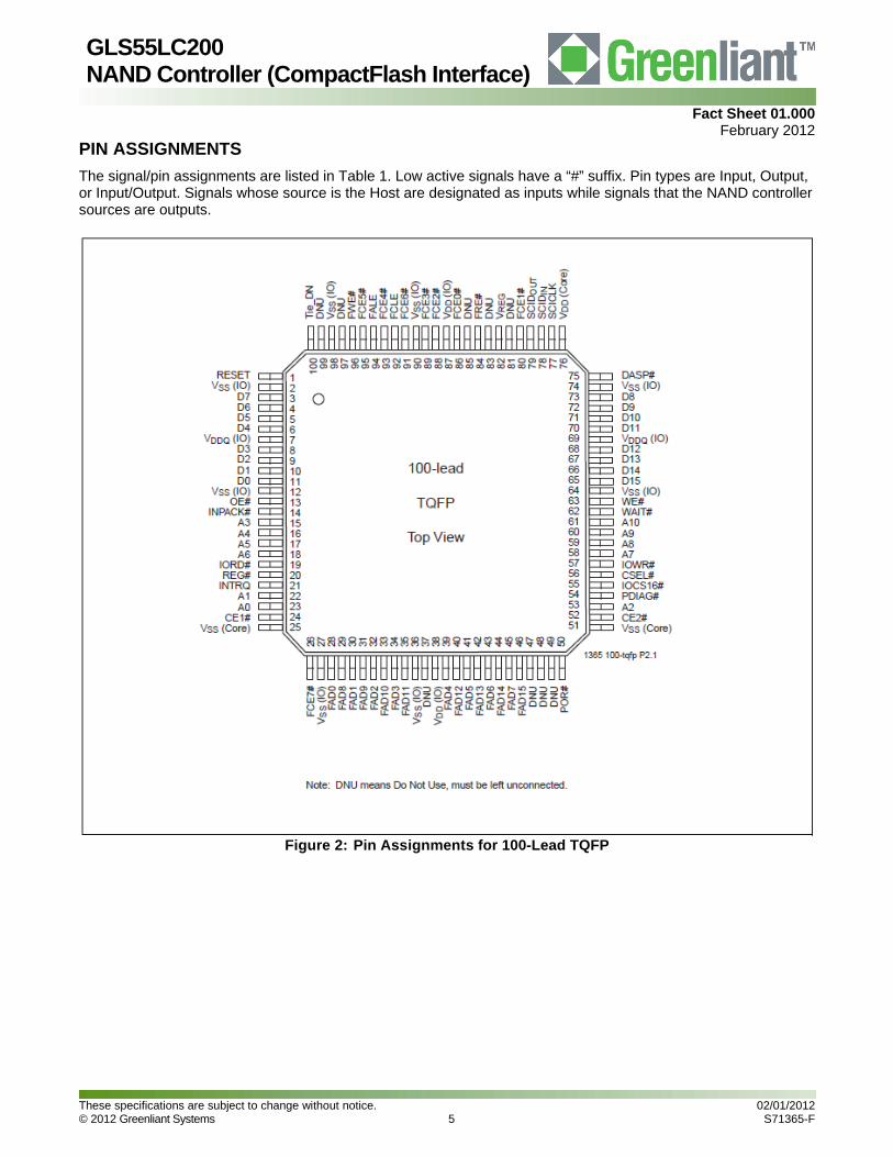
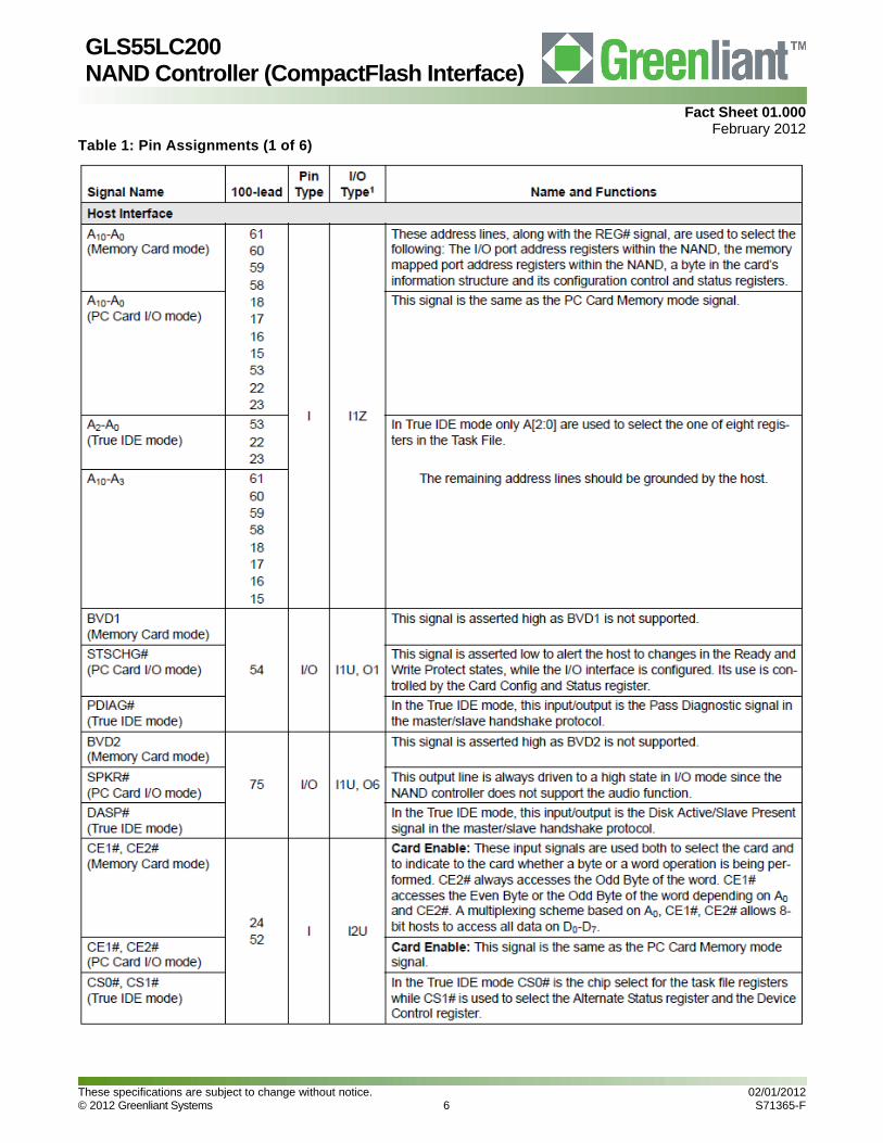
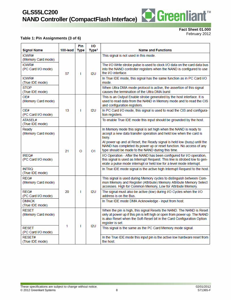
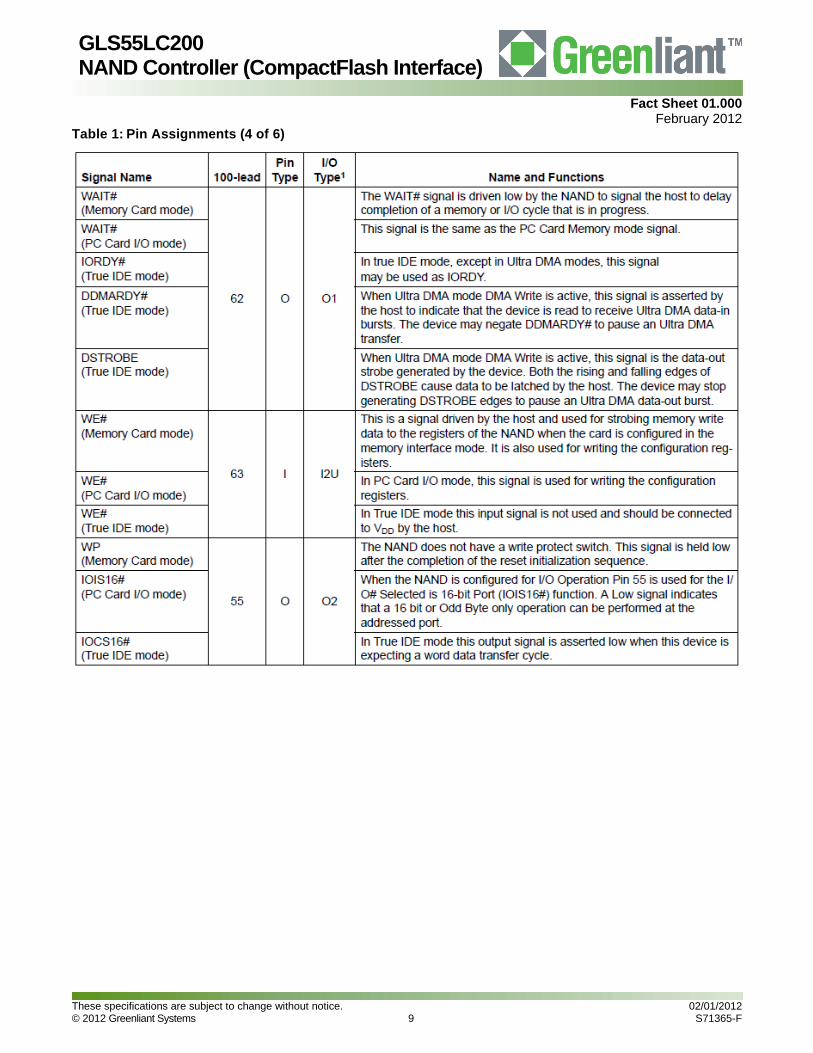
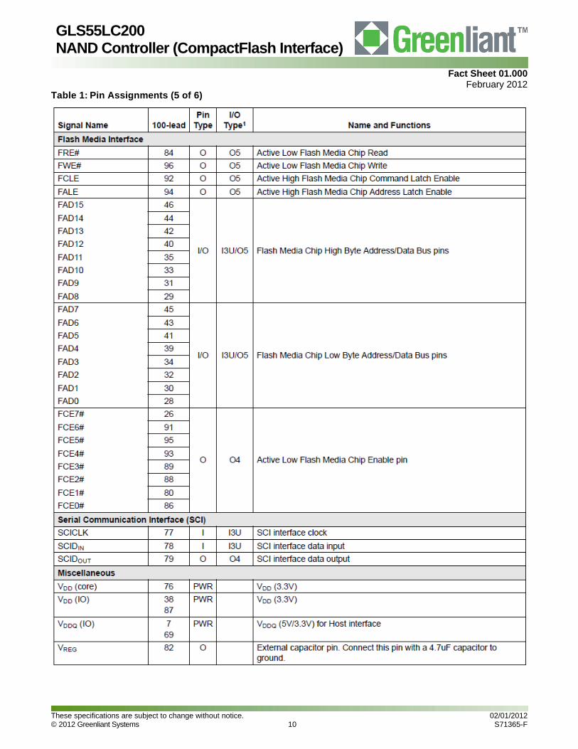
The signal/pin assignments are listed in Table 1. Low active signals have a “#” suffix. Pin types are Input, Output, or Input/Output. Signals whose source is the Host are designated as inputs while signals that the NAND controller sources are outputs.
Figure 2: Pin Assignments for 100-Lead TQFP
Fact Sheet 01.000 February 2012
These specifications are subject to change without notice. 02/01/2012 © 2012 Greenliant Systems 6 S71365-F
GLS55LC200 NAND Controller (CompactFlash Interface)
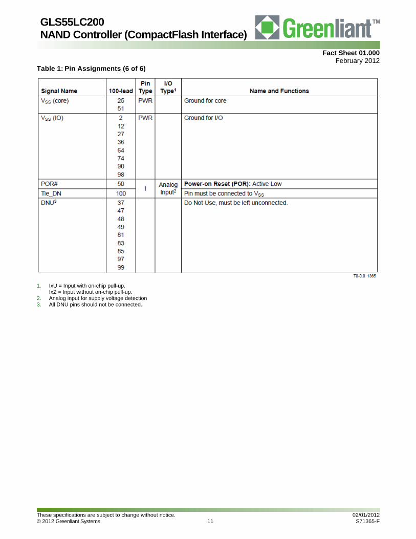
Table 1: Pin Assignments (1 of 6)

Fact Sheet 01.000 February 2012
These specifications are subject to change without notice. 02/01/2012 © 2012 Greenliant Systems 7 S71365-F
GLS55LC200 NAND Controller (CompactFlash Interface)
Table 1: Pin Assignments (2 of 6)
Fact Sheet 01.000 February 2012
These specifications are subject to change without notice. 02/01/2012 © 2012 Greenliant Systems 8 S71365-F
GLS55LC200 NAND Controller (CompactFlash Interface)
Table 1: Pin Assignments (3 of 6)
Fact Sheet 01.000 February 2012
These specifications are subject to change without notice. 02/01/2012 © 2012 Greenliant Systems 9 S71365-F
GLS55LC200 NAND Controller (CompactFlash Interface)
Table 1: Pin Assignments (4 of 6)
Fact Sheet 01.000 February 2012
These specifications are subject to change without notice. 02/01/2012 © 2012 Greenliant Systems 10 S71365-F
GLS55LC200 NAND Controller (CompactFlash Interface)
Table 1: Pin Assignments (5 of 6)
Fact Sheet 01.000 February 2012
These specifications are subject to change without notice. 02/01/2012 © 2012 Greenliant Systems 11 S71365-F
GLS55LC200 NAND Controller (CompactFlash Interface)
Table 1: Pin Assignments (6 of 6)
1. IxU = Input with on-chip pull-up.
IxZ = Input without on-chip pull-up. 2. Analog input for supply voltage detection 3. All DNU pins should not be connected.
Fact Sheet 01.000 February 2012
These specifications are subject to change without notice. 02/01/2012 © 2012 Greenliant Systems 12 S71365-F
GLS55LC200 NAND Controller (CompactFlash Interface)
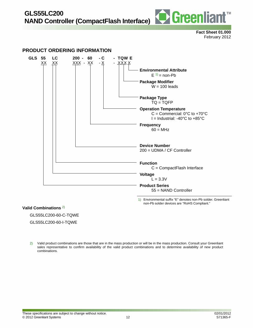
PRODUCT ORDERING INFORMATION
GLS 55 LC 200 - 60 - C - TQW E XX XX XXX - XX - X - X X X X
Environmental Attribute E 1) = non-Pb
Package Modifier W = 100 leads
Package Type TQ = TQFP
Operation Temperature C = Commercial: 0°C to +70°C I = Industrial: -40°C to +85°C
Frequency 60 = MHz
Device Number 200 = UDMA / CF Controller
Function C = CompactFlash Interface
Voltage L = 3.3V
Product Series 55 = NAND Controller
1) Environmental suffix “E” denotes non-Pb solder. Greenliant non-Pb solder devices are “RoHS Compliant.”
Valid Combinations 2)
GLS55LC200-60-C-TQWE
GLS55LC200-60-I-TQWE
2) Valid product combinations are those that are in the mass production or will be in the mass production. Consult your Greenliant sales representative to confirm availability of the valid product combinations and to determine availability of new product combinations.

Fact Sheet 01.000 February 2012
These specifications are subject to change without notice. 02/01/2012 © 2012 Greenliant Systems 13 S71365-F
GLS55LC200 NAND Controller (CompactFlash Interface)
PACKAGING DIAGRAM
Figure 3: 100-lead Thin Quad Flat Pack (TQFP)
Greenliant Package Code: TQW
Fact Sheet 01.000 February 2012
These specifications are subject to change without notice. 02/01/2012 © 2012 Greenliant Systems 14 S71365-F
GLS55LC200 NAND Controller (CompactFlash Interface)
REVISION HISTORY Revision Description Date
01.000 Initial release of Fact Sheet February 1, 2012
© 2012 Greenliant Systems. All rights reserved.
Greenliant, the Greenliant Logo and NANDrive are trademarks of Greenliant Systems. CompactFlash is a trademark of the CompactFlash Association. All other trademarks and registered trademarks are the property of their respective owners.
Specifications are subject to change without notice. Memory sizes denote raw storage capacity; actual usable capacity may be less.
Greenliant makes no warranty for the use of its products other than those expressly contained in the Greenliant Terms and Conditions of Sale.
www.greenliant.com