giant magneto-impedance and its …giant magneto-impedance and its applications c. tannous and j....
TRANSCRIPT

arX
iv:p
hysi
cs/0
2080
35v2
[ph
ysic
s.in
s-de
t] 3
Apr
200
3
GIANT MAGNETO-IMPEDANCE AND ITS APPLICATIONS
C. Tannous and J. Gieraltowski
Laboratoire de Magnetisme de Bretagne,
CNRS UMR-6135, Universite de Bretagne Occidentale,
BP: 809 Brest CEDEX, 29285 FRANCE,
Tel.: (33) 2.98.01.62.28, FAX:(33) 2.98.01.73.95 E-mail:[email protected]
Abstract
The status of Giant Magneto-Impedance effect is reviewed inwires, ribbons and multilayered soft fer-
romagnetic thin films. After establishing the theoretical framework for the description of the effect, and
the constraints any material should have in order to show theeffect, experimental work in wires, ribbons
and multilayered thin films is described. Existing and potential applications of the effect in electronics and
sensing are highlighted.
PACS numbers: 75.70.-i, 75.70.Ak, 85.70.Kh, 07.55.Ge
Keywords: Magnetic Materials. Transport. Magneto-impedance. Sensors. Wires. Thin films.
1

I. INTRODUCTION
Magnetoimpedance (MI) consists of a change of total impedance of a magnetic conductor
(usually ferromagnetic) under application of a static magnetic field Hdc. When an ac current,
I = I0ejωt of magnitudeI0 and angular frequencyω (= 2πf , with f the ordinary frequency)
flows through the material, it generates, by Ampere’s Law, atransverse magnetic field inducing
some magnetization. At low frequency, the change in the transverse magnetization generates an
additional inductive voltageVL across the conductor:V = RI + VL whereR is the resistance.
Hence MI can be written asZ = R + jωφ/I, where the imaginary part is given by the ratio
of magnetic flux to ac current and MI field dependence is related to the transverse permeability.
When frequency increases the current gets distributed nearthe surface of the conductor, changing
both resistive and inductive components of the total voltage V . The field dependence of MI is
dictated by skin depthδs = c√2πωσµ
wherec is the velocity of light,σ the conductivity andµ the
permeability (For non magnetic ordinary metals,µ = 1). The current distribution is governed not
only by the shape of the conductor and frequency but also the transverse magnetization depending
onHdc.
Typically MI increases with frequency, attains a maximum atfrequencies for which the skin
effect is strong (δs << a wherea is a characteristic length scale such as the wire radius or
ribbon/film thickness) and then decreases since permeability becomes insensitive to the field at
high enough frequency.
MI effect is ordinarily weak and did not attract much attention in the past. Interest in MI was
triggered in the early 90’s when Panina et al. [1] and Beach etal. [2] reported a very large (Giant)
MI effect in amorphous ferromagnetic FeCoSiB wires with small magnetic fields and at relatively
low frequencies (see Fig. I). This shows that a large variation of the MI is observable in a finite
frequency range for reasons that will be explained in later sections. Later on, Machado et al. [3]
observed a smaller effect in Fe4.6Co70.4Si15B15 thin films and Beach et al. [4] in ribbons.
The dramatic variation of the MI (that can reach in some casesvalues larger than 800%) with
small magnetic fields (a few Oersteds) and at relatively low frequencies (tens of MHz) in widely
available materials is the origin of the interest in the Giant MagnetoImpedance (GMI) effect.
2

GMI materials share the property of being magnetically soft(easy to magnetize) and are
now available as wires (typical diameter of the order of a mm), microwires (typical diameter
of the order of a micron), ribbons, magnetically coated metallic (usually nonmagnetic) wires
(tubes), thin films and multilayers, albeit, the effect itself occurs with widely differing magnitude
depending on the geometry, the constituent materials and their layering.
In order to clearly identify GMI, several observations should be made:
1. A very large change (of the order of at least 100% variation) of the impedance should occur
with an external dc magnetic fieldHdc. The change expressed in % is defined by the largest
value of the ratio:
r(Hdc) = 100× |Z(Hdc)− Z(Hsat)|/|Z(Hsat)| (1)
whereZ(Hdc) is the impedance measured in the presence of the dc magnetic fieldHdc and
Z(Hsat) is the impedance measured at the saturation limit when the magnetization does not
change any longer with the applied field.
2. The external dc magnetic fieldHdc should be on the order of a few Oersteds only (see Table
I on magnetic units and quantities).
3. The frequency range is on the order of MHz or tens of MHz (excluding any effect based on
Ferromagnetic Resonance (FMR) where the frequencies are typically in the GHz range [5]).
In many materials this means that the skin depthδs (typically microns at these frequencies)
is larger than the thickness of the material (typically a fraction of a micron). When the
frequency is in the GHz,δs is generally very small with respect to the thickness. It should
be stressed that in ordinary metals, the skin depth does not depend on permeability, whereas
in magnetic materials, the behavior of the permeability on geometry (see for instance section
IV), temperature, stress, composition and so on, is reflected in the skin depth. In addition,
permeability might be changed by post-processing the material after growth with annealing
under presence or absence of magnetic field or mechanical stress...
GMI is aclassical phenomenonthat can be explained thoroughly on the basis of usual electro-
magnetic concepts [6, 7, 8] in sharp contrast with Giant Magnetoresistance (GMR) effect where
3

resistance is changed by a magnetic field. GMR requires Quantum Mechanical concepts based
on the spin of the carriers and their interactions with the magnetization of the magnetic material.
Several general conditions must be satisfied by any materialin order to show a GMI.
1. The material should be magnetically soft. That is, it should be easily magnetised or in other
words must have a relatively narrow hysteresis curve implying, in general, small losses in
the course of the magnetization cycle.
2. The material should have a well defined anisotropy axis. That means there must be a direc-
tion along which the magnetization of the material lies on the average (easy axis). However
the value of the anisotropy fieldHk (see Fig. II) should be relatively small (on the order of
a few Oersteds). The typical ratio ofHk to Hc must be about 20. That insures observation
of large magnetoimpedance effects, typically.
3. The coercive fieldHc must be small (fraction of an Oersted) and the hysteresis loop thin and
narrow. SinceHc and the shape of the hysteresis loop change (see Fig. II) withthe angle the
magnetic field makes with the easy axis (or Anisotropy axis) of the material, these are taken
at the reference point when the field is along the easy axis.
4. The ac currentI = I0ejωt, injected in the material, should be perpendicular to the easy axis
(or anisotropy direction) and the magnetic field it createsHac should be small with respect
toHk (See Table I on magnetic units and quantities).
5. The material must have a small resistivity (≤ 100µΩ.cm ) since it carries the ac current. This
is important, since many magnetic materials have large resistivities. Amorphous metals are
interesting in that respect since, typically, their resistivities at room temperature are in the
100µΩ.cm range.
6. The material should have a large saturation magnetization Ms in order to boost the interac-
tion with the external magnetic field.
7. Above arguments are equivalent to a very large permeability at zero frequency (the ratio
Ms/Hk gives a rough indication for this value). This means several1000’s (see Table II).
8. The material should have a small magnetostriction (MS). This means, mechanical effects
caused by application of a magnetic field should be small. Mechanical stress due to MS
4
alters the soft properties of the material by acting as an effective anisotropy. This alters
the direction of the anisotropy, displacing it from the transverse case and thereby reducing
the value of the MI. Typical case materials are displayed along with their MS coefficient in
Table II.
The general theory of the MI effect is widely available in classic textbooks [9] (for a long
cylinder) and it has been shown experimentally that a large MI often occurs at frequencies of a
few MHz. Changing the dc biasing fieldHdc, the maximum|Z| can be as large as a few times
the value ofRdc the dc resistance. At low frequency|Z| has a peak aroundHdc ∼ 0 and as
the frequency increases, the peak moves towardHdc ∼ ±Hk whereHk is the anisotropy field.
Therefore,|Z| as a function ofHdc possesses a single or a double peak as the frequency increases
(Fig. III). When the direction of the anisotropy field is welldefined the peaks are sharp.
The behavior of|Z| versusHdc follows very closely the behavior of the real part of the
transverse permeability versusHdc as we will show in later sections on wires and ribbons. Ther-
fore it is very important to develop an understanding for theprocesses controlling the permeability.
Material permeability depends on sample geometry, nature of exciting field, temperature,
frequency, stress distribution in the material as well as internal configuration of the magnetization
that might be altered by processing or frequency. For instance, some materials should be annealed
under the presence of a magnetic field or a mechanical stress in order to favor some direction for
the magnetization or to release the stress contained in them.
Regarding frequency, when it is large enough (> 1MHz is sufficient in many materials)
Domain Wall Displacements (DWD) are considerably reduced by eddy-currents and therefore
magnetization varies by rotation or switching as if in a single domain (see Fig. II). As a conse-
quence, the rotational motion of the magnetization controls the behaviour of the permeability,
through the skin depth.
Consideringa as a typical thickness (in the case of films/ribbons) or radius (in the case of
wires or microwires), frequencies in the tens of MHz, lead toδs > a for the observation of GMI.
This condition depends strongly on geometry. For instance,δs > a in 2D structures like films
is satisfied at much higher frequencies (GHz) than in 1D structures like wires. This is simply
5

due to the optimal circular shape of wires that contains in anoptimal fashion the flux while,
simultaneously, carrying the ac current.
In terms of GMI performance, multilayered films (such as F/M/F where F is a ferromagnet
and M is metallic non magnetic material) are preferred with respect to single layered films since
they allow to inject the ac electric current in the metallic layer and sense the magnetic flux in
neighbouring or sandwiching magnetic layers. These can be in direct contact with the metallic
layer or separated from it by an insulator or a semiconductor. Flux closure, that increases GMI,
occurs when the width of the film (transverse with respect to the ac current) is large or that the
metallic layer is entirely buried in the magnetic structureto trap the flux.
The progress of GMI is thrusted towards the increase of the largest value of the ratior(Hdc)
and the sensitivity given by the derivative of the ratio withrespect to the field (see Table III for
some illustrative values).
This sensitivity is simply estimated by looking at the behaviour of the permeabiltyµ′t versus
Hdc as the frequency is changed. We ought to have a large variation of µ′t aboutHdc ∼ 0. This
happens, in general, at low frequencies that is whenδs > a. At high frequencies, we will show
in later sections that this sensitivity is either lost or onehas to go to higherHdc to observe it
hampering the use of the effect in small magnetic field detection.
Applications of GMI range from tiny magnetic field detectionand sensing (such as magnetic
recording heads) to magnetic field shielding (to degauss Cathode Ray Tubes (CRT) monitors).
The reason is that GMI materials, being soft, possess large permeabilities that are required in
magnetic shielding.
This work is organised as follows: In section II, a general discussion on soft materials is pre-
sented; in section III, GMI in wires is described. In sectionIV, GMI in films and ribbons is
dicussed. Section V highlights potential applications of GMI effect in Electronic ans Sensing
devices while Section VI bears conclusions and perspectives of GMI.
6

II. SOFT FERROMAGNETIC MATERIALS FOR GMI
Soft ferromagnetic materials (SFM) used in GMI applications play a key role in power
distribution, make possible the conversion between electrical and mechanical energy, underlie
microwave communication, and provide both the transducersand the active storage material for
data storage in information systems. The fingerprint of any magnetic material is its hysteresis
loop (HL) whose characteristic shape stems from two essential properties of magnetic materials:
Non-linearity and delay between input and output signals. Non-linearity is given by the shape
of the loop whereas the delay is given by the width of the HL. The quantities associated with
the HL are displayed in Fig. II. In general, magnetic materials being anisotropic their HL width
varies with the angle the external magnetic field makes with some given direction. The easy axis
direction is defined as the direction for which the HL width (or coercive fieldHc) is largest.
The coercive fieldHc represents the effort to demagnetise any magnetic material. For instance,
hard magnetic materials exhibit large resistance to demagnetization and are therefore used in
materials requiring permanent magnets whereas SFM are usedin devices demanding little effort
to demagnetise or remagnetise. Hard magnets are used as permanent magnets for many electrical
applications. Some rare-earth alloys based on SmCo5 and Sm(Co, Cu)7.5 are used for small
motors and other applications requiring an extremely high energy-product magnetic materials.
Fe-Cr-Co alloys are used in telephone receivers and Nd-Fe-Bis used for automotive starting motor.
In contrast, SFM possess a narrower loop than hard materialsand the area within the hysteresis
curve is small. This keeps the energy losses small, during each magnetic cycle, in devices based
on these materials.
In order to qualify the different requirements for read heads and storage media in magnetic
recording, an area belonging to the application portfolio of SFM (besides sensing and shielding),
Table IV displays the desired characteristics.
SFM have high permeability (i.e. easily magnetized) with a low coercivity (i.e. easily
demagnetized). Examples of soft ferromagnetic materials include Fe alloys (with 3 to 4% Si)
used in motors and power transformers and generators. Ni alloys (with 20 to 50% Fe) used
7

primarily for high-sensitivity communications equipment. This illustrates the versatility of SFM
applications that range from mechanical to electrical and from power to communications systems.
SFM exhibit magnetic properties only when they are subject to a magnetizing force such as
the magnetic field created when current is passed through thewire surrounding a soft magnetic
core. They are generally associated with electrical circuits where they are used to amplify the
flux generated by the electric currents. These materials canbe used in ac as well as dc electrical
circuits.
Several types of SFM exist:
1. Soft mono and polycrystalline ferrites
2. Powder composite magnetic materials
3. Rapidly quenched ferromagnetic materials
4. Amorphous magnetic materials
5. Nanocrystalline magnetic materials
The soft ferromagnetic behavior in these materials arises from a spatial averaging of the mag-
netic anisotropy of clusters of randomly oriented small particles (typically< fraction of a micron).
In some cases, the MS of these materials is also reduced to near zero.
Metallic glasses obtained by rapid quench (e.g. splat-cooling) are magnetically very soft. This
property is used in multilayered metallic glass power transformer cores.
Amorphous magnetic alloys such as CoP first reported in 1965 and splat-cooled materials with
attractive soft ferromagnetic properties are based eitheron 3d transition metals (T) or on 4f rare-
earth metals (R). In the first case, the alloy can be stabilized in the amorphous state with the use of
glass forming elements such as boron, phosphorus and silicon: Examples include Fe80 B20, Fe40
Ni40P14 B6, and Co74 Fe5 B18 Si3 (Tx M1−x, with 15 < x < 30 at %, approximately). The tran-
sition metals of late order (TL where TL=Fe, Co, Ni) can be stabilized in the amorphous state by
alloying with early order transition metals (TE) of 4d or 5d type (TE= Zr, Nb, Hf): some examples
are Co90 Zr10 , Fe84 Nb12 B4 , and Co82 Nb14 B4 (TE1−x TLx, wherex is roughly5 < x < 15 at %).
Nanocrystalline soft magnetic materials are derived from crystallizing amorphous ribbons of a
specific composition such as the (Fe, B) based alloy family. This class of materials is characterized
8

by 10-25 nm sized grains of a body-centered-cubic (Fe, X) phase consuming 70-80% of the total
volume, homogeneously dispersed in an amorphous matrix.
Two families of alloys show the best performance characteristics and have emerged as the best
candidates to major SFM applications: Fe-Cu-Nb-B-Si (the ”Finemet” family, see Table III) and
Fe-Zr-(Cu)-B-(Si) (the ”Nanoperm” family). The Finemet family is characterized by an optimum
grain size of about 15 nm, exhibits good properties at high frequencies and is comparable to some
of the best (and relatively costly) Co based amorphous materials. On the other hand, the grain
sizes consistent with optimum performance are larger, around about 25 nm, in the Nanoperm
family. The distinguishing feature of the Nanoperm family of alloys is the very low energy loss
exhibited at low frequencies (60 Hz), offering the potential for application in electrical power
distribution transformers.
A typical amorphous alloy with a small MS coefficientλs, is Co70.4 Fe4.6 Si15 B 10. It is
obtained by alloying FeSiB that has a positiveλs = 25. 10−6 with CoSiB that has a negative
λs = −3. 10−6 coefficient. Some materials that result from this alloying can reach a very small
value ofλs. For instance, (Co0.8 Fe0.06)72.5 Si12.5 B 15 hasλs ∼ −10−7 that can be considered
as zero since typical values ofλs are units or tens of10−6. This was obtained by varying
systematically the concentrationx in the compound (Co1−x Fex)72.5 Si12.5 B15. Starting with
x = 0 the MS coefficientλs = −3.0 10−6 decreases steadily to a near zero valueλs = −10−7
for x = 0.06. Let us indicate, at this point, that a commercial product exists called Vitrovac
6025 ®with the composition Co66 Fe4 Mo2 Si16 B12 that exhibits a value [10] ofλs = −1.4 10−7.
A small negative value ofλs is exploited in wires, as discussed in the next section, produces a
magnetization profile that is circular in a plane perpendicular to the wire axis whereas a positive
λs produces a radial magnetization profile.
III. GMI IN WIRES
The search for GMI in soft magnetic wires and microwires is a topic of interest related to
possible applications as tiny field sensors.
9

At low frequencies (weak skin effect or large skin depth), the first order expansion term of the
impedanceZ = R(ω) + jX(ω) versus frequency is responsible for the voltage field dependence.
This term is represented by an inductance, which is proportional to the transverse permeability.
When the skin effect is strong, the total impedance including resistanceR and reactanceX is field
dependent through the penetration depth.
The general theory of the MI effect in a long cylinder is widely available in classic textbooks
[9] and it has been shown experimentally that a large MI oftenoccurs at frequencies of a few MHz.
Changing the dc biasing fieldHdc, the maximum|Z| can be as large as a few times the value of
Rdc for amorphous wires. Following Beach et al. [4] the behaviour of the permeability can be
understood on the basis of a simple phenomelogical model based on a single relaxation timeτ for
the magnetization that yields for the permeability:
µt(ω,Hdc) = µ′t + jµ”t; µ′
t = 1 +4πχ0(Hdc)
1 + ω2τ 2, µ”t =
4πχ0(Hdc)ωτ
1 + ω2τ 2(2)
The behaviour ofµ′t depicted in Fig. IV indicates that the strongest variation of µ′
t with Hdc
happens at low frequencies as required for a sensitive sensor whereas the variation gets totally
smeared out at large frequencies. It also illustates the existence of a finite frequency range for the
GMI effect as already observed in Fig. I. The range is determined by the inverse time 1/τ that
controls relaxation processes of the transverse magnetization.
While GMR is usually attributed to the differential scattering of conducting electrons whose
spins make particular angles with the local magnetization of different scattering centers, it was
believed, like GMR, this effect also resulted from the electron scattering by ac current-induced
domain wall oscillations. Many different models exist for the description of permeability of metal-
lic samples. Such models start with a uniform dc permeability throughout the sample, and then
consider a class of domain structures with a magnetization process of DWD or domain magnetiza-
tion rotations (DMR). In the case of ac impedance, standard quantitative models are used without
considering domain structures. Therefore, some current explanations of MI have to be made based
on usual considerations with some additional modificationsto include concepts of DWD, DMR,
ferromagnetic resonance, and magnetic relaxation. For a straight wire of radiusa, conductivityσ
and permeabilityµ (see Fig. V) the expression for impedance is given by [9]:
Z
Rdc=
R + jX
Rdc=
ka
2
J0(ka)
J1(ka)(3)
10

whereJi is the i-th order Bessel function andk = (1 + j)/δs where the skin depth is given by
δs =c√
2πωσµ. c is the speed of light andσ the conductivity.
Since the ac current is applied along the wire axis perpendicularly to the anisotropy (Fig. V), it
is again the transverse permeabilityµ that is considered here. In order to show that the behavior
of Z is dictated by the permeability, let us consider firstly the low frequency case, i.e.ka << 1.
Expanding the Bessel functions, yields:
Z
Rdc= 1 +
1
48(a
δs)4
− j1
4(a
δs)2
(4)
In the opposite high frequency case (δs << a or ka >> 1), takinga ∼ 1mm whereasδs ∼ 1µ
m, we can expand the Bessel function to obtain:
Z
Rdc= (1 + j)
a
2δs(5)
This indicates thatZRdc
could reach a value of several 1000’s at high frequencies. The same
result is obtained in the case of microwires by rescaling alllengths (since we have, in this case,
a ∼ 1µ m). It should be pointed out that since the ac current is alongthe wire axis, the magnetic
field produced is circular along or against the rotational magnetization profile (see Fig. V). Note
that at the frequencies of interest (> 1MHz), where we have the largest sensitivity toHdc,
eddy-currents heavily damp DWD.
In wires made of materials having a small negativeλs, the magnetization and anisotropy field
Hk run in a circular fashion in a plane transverse to the ac current as illustrated in Fig. V. The dc
field Hdc acts to realign the magnetization along its direction, decreasing therefore the transverse
permeability. Therefore, a positiveλs cannot be used for GMI since the magnetization profile is
rather radial.
The skin depth dependent classical formula does not accountfor the presence of domain walls
that can alter the scattering of the carriers. Panina et al. [1] and Chen et al. [11] accounted for
domain wall scattering and showed that the latter is efficient when the inter-domain distanceλ (see
Fig. V) to the wire radiusa ratio λ/a ≤ 0.1 for frequencies∼ 1MHz or greater. Introducing a
parameterθ = a√σµω, they argue that a change of MI by a factor of 10 (assuming a change of
θ2 by a factor between 7 and 700) yields a change ofµ/µ0 by a factor of 100 to 10, 000. Using a
resistivityρ = 1/σ =125µΩ.cm and 2a=0.124 mm, the frequencyf ∼ 3.1 MHz yields a factor
11

of 4 to 10 change in|Z|. Chen et al. [11] proved also that the classical limit is recovered when
λ/a ≤ 0.01. The interpretation of a single or a double peak in the MI versusHdc is interpreted
as resulting from scattering by DMR. The scattering increases asHdc gets closer to the anisotropy
field Hk and then decreases after reaching its maximum forHdc ∼ ±Hk. Wires with very small
anisotropy possess a single peak since the scattering maximum occurs atHdc ∼ 0. Frequency
effects produce the same result as seen in Fig. III.
In the case of GMI effect in coated tubes such as the electroplated FeNi, FeNiCo, and CoP
microwires, Kurlyandskaya et al. [12] found a huge enhancement factor approaching 800% in
Fe20Co6Ni74 layers (1µ m-thick) electroplated onto CuBe nonmagnetic microwire (100 µm di-
ameter) at a frequency of 1.5 MHz. That shows the way for producing the largest GMI in these
systems.
IV. GMI IN RIBBONS AND THIN FILMS
Sputtered or otherwise produced films or ribbons possess several advantages with respect to
wires due to the possibilities of size reduction and increase of efficiency. Nevertheless, oblong or
elongated ribbon or thin film geometries are preferred in order to emulate the wire case where the
largest GMI ratios were obtained.
Since the main ingredients of GMI are a metal that carries an ac current and a nearby magnetic
material that must sense strongly the flux, 2D materials or multilayers offer more flexibility than
wires and experimentally, several excitation configuration become possible when we are dealing
with a ribbon or a film.
The general MI measurement configuration (longitudinal, perpendicular, transverse) in ribbons
and films is shown in Fig. VI. In films and ribbons, the domain wall configuration is similar to
what goes on in wires in the sense domain walls are transversewith respect to the ac current.
In Fig. VII neighbouring domains have magnetizations pointing in different directions and the
magneto-impedance effect result from averaging over transverse domains like in the wire case.
12

When a probe currentI0ejωt is applied to a film of thickness2a, the impedance is written as:
Z
Rdc= jka coth(jka), (6)
whereRdc is the dc resistance of the film andk = (1+ j)/δs with δs the skin depth given by, as
before,δs = c√2πωσµ
. Since the current is applied (in the ribbon case) along the ribbon axis, again
the transverse permeability is considered. As in the wire case, it is possible to expandZRdc
at low
(or ka << 1) and high frequencies (orka >> 1) and show thatµt controls its behavior withHdc.
At low frequencies (ka << 1), we get:
Z
Rdc= 1− 2j
3(a
δs)2
(7)
whereas, at high frequencies (ka >> 1):
Z
Rdc= 1− j
a
δs(8)
The domain wall configuration (see Fig. VII) permits to estimate the permeability in the
case of weak anisotropy field (Hk small but finite). It should be stressed that domains,Hk and
permeability are all transverse. WhenHdc is longitudinal, it plays the role of a hard axis field
since it is acting on the magnetization, to rotate it, hence decreasing the transverse permeability,
similarly like in wires.
In order to increase the MI response, multilayers are preferred to single layered films/ribbons.
If a sandwiched metallic layer carries the ac current that creates the flux in the neighbouring
magnetic layers, the MI effect is considerably enhanced (Table III). Moreover, when the width2b
is large (Fig. VII) the ac flux loop is closed and stray magnetic fields small [13].
Multilayers of Permalloy (Ni81Fe19 denoted as Py) and Ag of the type[Py(xA)/Ag (y A)]n with
thickness x = 107A and 88A, y= 7 A and 24A and the number of layers n=15 and 100 were
grown by Sommer et al. [14] with magnetron sputtering techniques. The case n=100 displayed
a GMI effect of the order of 5 to 25 %. The thickness of the Py layer has a strong effect on the
coercive field and consequently on the softness of the material. The coercive fieldHc varies from
0.85 Oersted for x=88A to reach 13.6 Oersted for x=5000A. As the Ag thickness varied from 7
to 24A the MI effect changed from single peak to double peak structure in a fashion akin to the
effect of frequency. Sommer and Chien [15] showed also that in the ribbon case, a double or a
13

single peak structure in the MI results from the direction ofthe applied magnetic fieldHdc. When
it is longitudinal (along the ribbon axis, see Fig. VII) a double peak atHdc ∼ ±Hkis observed,
but when it is transverse the demagnetization factor perpendicular to the ribbon axis becomes
important. That is responsible of an apparentlongitudinalpermeability that gives birth to a single
peak MI. The ribbon MI is similar to the wire case, however MI in single layer films remains small
and it is still an open problem to find ways to increase it dramatically like in coated microwires.
Nevertheless, when multilayers are used (see Table III) theGMI ratio may attain 700%. This
enhancement is due to the electrical insulation of the metallic layer carrying the ac current by
sandwiching it with SiO2 layers, the outer magnetic layers embodying the ac inductance created
by the current.
V. APPLICATIONS OF GMI IN ELECTRONICS AND SENSING
Since GMI uses soft magnetic materials possessing a large permeability, the first immediate
application is in devices related to magnetic shielding since it requires the soft properties of the
material. A host of other applications involves the GMI per se.
The first of these applications are the detection of very small magnetic fields. In order to have
a general idea of the scale of current magnetic Fields Table Vdisplays some orders of magnitude
of natural and artificial fields.
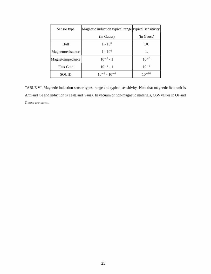
Detection of magnetic field is also important and magnetic field sensors (see Hauser et al. [16])
are broadly classified in three categories (see Table VI):
1. Medium to large field detection by Hall and magnetoresistive devices.
2. Small to medium magnetic field detection by magnetoimpedance and Flux Gate sensors.
3. Very small to small magnetic field detection by SQUID’s (Superconducting QUantum In-
terference Devices).
The possible devices are recording read heads, magnetic guidance devices in vehicles, boats
and planes (with or without GPS, i.e. Global Positioning System), brain imaging (magneto-
encephalogram or MEG devices) and heart mapping (magneto-cardiogram or MCG devices) etc...
14

The detection of the Earth magnetic field has a host of applications for instance in Petroleum or
minerals exploration or in shielding used for Degaussing ofHigh performance CRT monitors...
The general features required for sensors are not only high sensitivity, flexibility, large bandwidth
and lost cost but linearity is also a desired feature. In order to increase the sensitivity of GMI de-
vices with respect to the dc magnetic field, devices were developed [17] possessing non-symmetric
variation of the MI with respect toHdc. The materials used are field annealed Co-based amorphous
ribbons (Co66 Fe4 Ni B14 Si15) (see Table III). The asymmetry of the MI profile allows a verysen-
sitive detection of the magnetic field specially aroundH ∼ 0 and when the asymmetry of the
profile is so sharp that it becomes step-like, we have a so-called ”GMI valve” based device. In
these devices, the sensitivity might be enhanced to reach 1000%/Oe (compare with values in Ta-
ble III). Asymmetry may also be induced by torsional stress such as in wires of Fe77.5Si7.5 B 15
[18]. Altering the GMI response with mechanical stress paves the way toward the development of
strain sensors that can be used in several areas of engineering and science.
VI. CONCLUSION
Good candidates for GMI are amorphous Cobalt rich ribbons, wires, glass covered microwires
and multilayers made of a metallic layer sandwiched betweenferromagnetic materials (with or
without intermediate insulating layers).
Zero-field annealing or annealing under a magnetic field or with the application of some
mechanical stress favors orienting the magnetization along a desired direction. In order to get a
fast reduction of the transverse permeability (see Fig. IV)under the application of an external
field Hdc, there must be an optimal distribution of the magnetizationaround the desired direction
[1] and that can be obtained with suitable growth or annealing conditions. Reduction of the
stress contained into the as-grown materials by sputteringor quenching can also be obtained with
annealing.
The current activity in GMI studies is oriented toward the development of devices using a built-in
magnetic field rather than an applied external field. This is reminescent of the p-n, Schottky,
heterojunctions etc... where the built-in field is electrical.
The discovery of magnetic bias produced a revolution in magnetism because of the many potential
applications in storage, sensing, spintronics... Nevertheless, there are other ways to produce
built-in magnetic fields. For instance Ueno et al. [19] produced susch an internal field by
15

superposing two sputtered films of Co72 Fe8 B 20 with crossed anisotropy axes, i.e. with the
anisotropy axis of the bottom layer making angles of opposite sign with some common direction.
While GMI in wires and ribbons is steadily progressing, the case of single layered films is still
lagging behind in favor of multilayered films. Ways must be developed in order to increase the
sensitivity of single or multilayered structures in order to reach the level observed in wires and
microwires. The range of applications will substantially explode once GMI in thin films will be
competitive with wires and ribbons.
Acknowledgement
The authors wish to acknowledge correspondance with P. Ripka and his kind providing of
re(pre)prints of his work as well as friendly discussions with A. Fessant regarding characterisation
and impedance measurements.
[1] L. V. Panina and K. Mohri, Appl. Phys. Lett. 65, 1189 (1994).
[2] R. S. Beach and A. E. Berkowitz, Appl. Phys. Lett. 64, 3652(1994).
[3] F. L. Machado, B. L. da Silva, S. M. Rezende and C. S. Martins, J. Appl. Phys. 75, 6563 (1994).
[4] R. S. Beach and A. E. Berkowitz, J. Appl. Phys. 76, 6209 (1994).
[5] M. R. Britel, D. Menard, L. G. Melo, P. Ciureanu, A. Yelon,R. W. Cochrane, M. Rouahbi and B.
Cornut, Appl. Phys. Lett. 77, 2737 (2000).
[6] D. Atkinson and P. T. Squire, J. Appl. Phys. 83, 6569 (1998).
[7] M. Knobel and K. R. Pirota, JMMM 242-245, 33 (2002).
[8] R. Valenzuela, M. Knobel, M. Vazquez and A. Hernando, J. Appl. Phys. 78, 5189 (1995).
[9] L. D. Landau and E. M. Lifshitz, Electrodynamics of Continuous Media, Pergamon, Oxford, p.195
(1975).
[10] N. Murillo, J. Gonzalez, J. M. Blanco, R. Valenzuela, J.M. Gonzalez and J. Echebarria, J. Appl. Phys.
81, 5683 (1997).
[11] D-X Chen, J.L. Munoz, A. Hernando and M. Vazquez, Phys. Rev. 57, 10699 (1998).
[12] G. V. Kurlyandskaya, J. M. Barandiaran, J. L. Munoz, J. Gutierrez, D. Garcia, M. Vazquez, and V. O.
Vaskovskiy, J. Appl. Phys. 87, 4822 (2000).
16

[13] A. Paton, J. Appl. Phys. 42, 5868 (1971).
[14] R. L. Sommer, A. Gundel and C. L. Chien, J. Appl. Phys. 86, 1057 (1999).
[15] R. L. Sommer and C. L. Chien, Appl. Phys. Lett. 67, 3346 (1995).
[16] H. Hauser, L. Kraus and P. Ripka, IEEE Inst. and Meas. Mag. 28 (2001).
[17] C.G. Kim, K.J. Jang, D.Y. Kim and S.S. Yoon: Appl. Phys. Lett. 75, 2114 (1999).
[18] G.H. Ryu, S.C. Yu, C. G. Kim, I.H. Nahm and S.S. Yoon, J. Appl. Phys. 87, 4828 (2000).
[19] K. Ueno, H. Hiramoto, K. Mohri, T. Uchiyama and L. V. Panina, IEEE Trans. Mag. 36, 3448 (2000).
17

FIGURES AND TABLES
0
0.2
0.4
0.6
0.8
1
0.01 0.1 1 10 100
Z(H
=0)
, Z(H
), |Z
(H)-
Z(0
)|/|Z
(0)|
f (MHz)
FIG. I: Normalised impedance Z(H=0) and Z(H) versus frequency for amorphous Fe4.3 Co68.2 Si12.5 B15
wire (30 micron diameter) withH=10 Oe. The upper monotonous curve (+) isZ(H = 0), the lower
monotonous curve (x) isZ(H) and the bumpy curve (*) is the ratio|Z(H) − Z(H = 0)|/|Z(0)|. The
largest ratio reaches 60 %. Note the finite frequency range where the large variation is observed. The figure
is adapted from Panina et al. [1].
M(
Mag
netis
atio
n)
H (Field)
M−H loop
Mr(remanant)
Hr
Ms(saturation)
Hc(coercive) Hk(anisotropy)
FIG. II: Single domain hysteresis loop obtained for an arbitrary angle,α, between the magnetic field and
the anisotropy axis. Associated quantities such as coercive fieldHc, remanent magnetizationMr and field
Hr (given by the intersection of the tangent to the loop at−Hc and theMr horizontal line) are shown. The
thick line is the hysteresis loop when the field is along the hard axis (α=90 degrees, in this case) andHk is
the field value at the slope break. Quantities such asHc, Mr andHr depend onα.
18

0
0.5
1
1.5
2
2.5
3
−3 −2 −1 0 1 2 3
|Z|/R
dc−
1Hdc/Hk
FIG. III: Variation of normalised impedance|Z|/Rdc versus magnetic fieldHdc at fixed low (single peak)
and high frequency (double peak). As the frequency increases, the peak shifts toward the anisotropy field
±Hk. That is why at low frequency a single peak is observed. The rounding of the peaks is due to a
distribution of the anisotropy field direction.
0
1000
2000
3000
4000
5000
6000
7000
0 20 40 60 80 100 120
µ t’
Hdc (Oe)
0 MHz1 MHz
10 MHz
FIG. IV: Variation of the transverse permeability versus magnetic fieldHdc. The physical quantities used
are the same of Beach et al. [2] such as the experimentally determined functionχ0(Hdc) and the inverse
relaxation time1τ = 10.45 MHz. The latter determines the range of variation of interest for the permeability.
19

λ
Hac
Hdc
2aI
FIG. V: Bamboo-like domain wall structure in a cylindrical wire with magnetization profiles counter-
rotating about a central core where the ac currentI circulates. It is the small negative value of MSλs
that induces a circumferential residual anisotropy through the inverse magnetostriction effect [1] producing
the circular magnetization profiles. The resulting circular anisotropy axis (easy axis), along the magnetiza-
tion is perpendicular to the direction of the ac current. Therefore, the dc fieldHdc plays the role of a hard
axis that damps magnetization and consequently decreases the permeability. A positiveλs results in a radial
magnetization profile that cannot be exploited in GMI applications.
Ribbon axis
HacI
Hdc (perp.)
HkHdc (long.)
Hdc (trans.)
FIG. VI: General magnetoimpedance measurement setup in an elongated ribbon. The static fieldHdc
might be longitudinal, transverse or perpendicular to the ac currentI = I0ejωt that creates the alternating
transverseHac. Hk is the anisotropy field, transverse to the ac current direction. WhenHdc is longitudinal,
it plays the role of a hard axis field like in wires that decreases the transverse permeability.
Hac
Hk
2b
F
M
F I
FIG. VII: Domain wall configuration in a multilayered structure. The magnetization direction is shown in
every domain. The ac current flows in the sandwiched metalliclayer, producing an ac flux in the surrounding
magnetic layers.
20

Physical Quantity SI CGS
Bohr magnetonµB 0.927 10−23A.m2 0.927 10−20emua
Vacuum permeabilityµ0 4π 10−7 V.s/A.m 1
Field Strength H A/m 4π 10−3 Oe
Example 80 A/m ∼ 1Oe
Polarisation or magnetization µ0Ms 4πMs
with saturation valueMs
ExampleMsb 1A/m 4π10−3 emu/cm3
InductionB B = µ0(H +M) B = H + 4πM
Example 1 Tesla= 1V.s/m2 104G
Susceptibility M = χH M = χH
Example χ = 4π χ = 1
Energy density of magnetic Field BH/2 BH/8π
Example 1J/m3 10erg/cm3
Energy of magnetic matter µ0HdM HdM
in an external field
Anisotropy constant K 105 J/m3 106 erg/cm3
Anisotropy Field HK = 2 Kµ0Ms
HK = 2 KMs
Example 106 A/m 4π103 Oe
Exchange Field JµB
JµB
Example 109 A/m 4π106 Oe
Demagnetising field in a thin film −Ms −4πMs
Energy density of µ0M2s /2 2πM2
s
Demagnetising field in thin film
Magnetostriction
coefficient ±λs ∼ 10−6 ±λs ∼ 10−6
aalso expressed in erg/OebIt is also expressed in Gauss with 1Gauss= 1emu/cm3
TABLE I: Correspondance between magnetic Units in the SI andCGS unit systems. Note that magnetic
field units are A/m and Oe and Induction’s are Tesla and Gauss.In vacuum or non-magnetic materials in
CGS values in Oe and Gauss are same. 21

Alloy Hc (mOe)µmax at 50 Hzmagnetostrictiona Coefficient
Fe80 B20 40 320, 000 λs ∼ 30.× 10−6
Fe81 Si3.5 B13.5 C2 43.7 260, 000
Fe40 Ni40 P14 B6 7.5 400, 000 λs ∼ 10.× 10−6
Fe40 Ni38 Mo4 B18 12.5-50 200, 000
Fe39 Ni39 Mo4 Si6 B12 12.5-50 200, 000
Co58 Ni10 Fe5 (Si, B)27 10-12.5 200, 000 λs ∼ 0.1× 10⁻⁶
Co66 Fe4 (Mo, Si, B)30 2.5-5 300, 000
aIt is defined asλs = δl/l, the largest relative change in length due to application ofa magnetic field
TABLE II: Examples of soft magnetic materials and their hierarchy according toλs. The main composition
is successively based on Fe, NiFe and finally Co. A commercialcompound, close to the last family, Vitrovac
6025 ®or Co66 Fe4 Mo2 Si16 B12 has [10]λs = −1.4 10−7
22

Material max(r(Hdc)) a max(dr(Hdc)/dHdc) (% /Oe) Frequency (MHz)
Amorphous microwire:
Co68.15 Fe4.35 Si12.5 B15 56 58.4 0.9
Finemet wireb 125 4
Amorphous wire:
Co68.15 Fe4.35 Si12.5 B15 220 1760 0.09
CoP multilayers
electroplated on Cu wire 230 0.09
Mumetalc, stripe 310 20.8 0.6
Textured
Fe-3% Si sheet 360 0.1
Amorphous ribbon:
Co68.25 Fe4.5 Si12.25 B15 400 1
Ni80 Fe20 electroplated
on non-magnetic CuBe microwire 530 384 5
Sandwich film:
CoSiB/SiO2/Cu/SiO2/CoSiB 700 304 20
FeCoNi electroplated
on non-magnetic CuBe microwire 800 1.5
ar(Hdc) = 100× |Z(Hdc)− Z(Hsat)|/|Z(Hsat)|bFe-Cu-Nb-B-Si familyc77% Ni, 16% Fe, 5% Cu, 2% Cr
TABLE III: Materials for GMI sensors: wires and films adaptedfrom Hauser et al. [16]. The GMI ratio is
given in the second column whereas the sensitivity with respect to the magnetic field is given by the largest
value of the derivative of the ratio (third column).
23

HL quantity Head coreRecording Media
Ms Large Moderate
Mr Small Large
Hc Small Large
S = Mr/Ms Small∼ 0 ∼ 1
Sc = (dMdH )H=Hc
Large
S∗ = 1− (Mr/Hc)Sc
∼ 1
TABLE IV: Requirements on read head and recording media fromHL. The parameters S and S* are the
remanant and the loop squareness respectively. S* represents the steepness of the HL at the coercive field,
i.e. the slope of the HL atHc is Sc = (dMdH )H=Hc
= Mr
Hc(1−S∗) . In practice a fairly square HL has S, S*
∼ 0.85.
Magnetic inductiona occurrence Typical Range Typical Range
Type of Induction (in Gauss) (in Tesla)
Biological
Body or brain of manb, animals...10−10 - 10−5 Gauss10−14 - 10−9 Teslac
Geological
Inside Earth 1010 Gauss 106 Tesla
On the Earth surface 10−4 - 1 Gaussd
Superconducting Coil > 25. 104 Gauss > 25 Teslas
amagnetic field is expressed in Oe and induction in Gauss.bThe magnetic induction of the Human Brain is about 10−13 TeslacHuman heart induction is around 10−10 TesladTransverse component of the Earth magnetic induction is 0.5Gauss
TABLE V: Natural and artificial magnetic induction in various systems. Note that magnetic field unit is
A/m and Oe and Induction is Tesla and Gauss. In vacuum or non-magnetic materials in CGS values in Oe
and Gauss are same.
24
Sensor type Magnetic induction typical rangetypical sensitivity
(in Gauss) (in Gauss)
Hall 1 - 106 10.
Magnetoresistance 1 - 106 1.
Magnetoimpedance 10−6 - 1 10−6
Flux Gate 10−6 - 1 10−6
SQUID 10−9 - 10−6 10−10
TABLE VI: Magnetic induction sensor types, range and typical sensitivity. Note that magnetic field unit is
A/m and Oe and induction is Tesla and Gauss. In vacuum or non-magnetic materials, CGS values in Oe and
Gauss are same.
25