george c. marshall marshall space flight center, of illustrations figure title page 1. spring-loaded...
TRANSCRIPT

NASA TECHNICALMEMORANDUM
NASA TM X- 64686
RELIABILITY OF HYBRID MICROCIRCUITDISCRETE COMPONENTS
By Robert V. Allen and Salvadore V. Caruso~A -Astrionics Laboratory
(NASA-TM-X-64 6 8 6 ) RELIABILITY OFMICROCIRCUIT DISCRETE COMPONENTS33 p HC :'
HYBRID(NASA)CSCL 09C
N73-16208
UnclasG3/10- 52566
October 1972-
NASA
George C. Marshall Space FligMarshall Space Flight Center,
Reproduced by
NATIONAL TECHNICALINFORMATION SERVICE
US Dep.rtment of CommerceSpringfield, VA. 22151
xht CenterAlabama
MSFC - Form 3190 (Rev June 1971)
https://ntrs.nasa.gov/search.jsp?R=19730007481 2018-06-12T10:44:25+00:00Z

rlUI"ICAI PORnDT STAlnARn TITL F PAIGE
1. REPORT NO. 2. GOVERNMENT ACCESSION NO. 3. RECIPIENT'S CATALOG NO.
TMX -646864. TITLE AND SUBTITLE 5. REPORT DATE
October 1972Reliability of Hybrid of Microcircuit Discrete Components 6. PERFORMING ORGANIZATION CODE
7. AUTHOR(S) 8. PERFORMING ORGANIZATION REPORT #Robert V. Allen and Salvadore V. Caruso
9. PERFORMING ORGANIZATION NAME AND ADDRESS 10. WORK UNIT NO.
George C. Marshall Space Flight CenterMarshall Space Flight Center, Alabama 35812 1 1. CONTRACT OR GRANT NO.
13. TYPE OF REPOR7 & PERIOD COVERED
12. SPONSORING AGENCY NAME AND ADDRESSTechnical Memorandum
National Aeronautics and Space AdministrationWashington, D. C. 20546 14. SPONSORING AGENCY CODE
15., SUPPLEMENTARY NOTES
Prepared by Astrionics.Laboratory, Science and Engineering
16. ABSTRACT
Hybrid microcircuit technology has rapidly become a standard technique in developmentand fabrication of electronic hardware. The most obvious reasons for the rapid acceptanceof hybrids are small size, reduced weight and higher reliability. The reliability of a hybridmicrocircuit is determined by factors such as wire bonding, interconnection techniques, thick-and thin-film processing, discrete component mounting, and hermetic sealing. Most of thesefactors can be controlled during fabrication cycles with proper process controls. However,since the hybrid manufacturer has little or no control on the design and fabrication of discretecomponents, these devices have the most paramount effect on microcircuit reliability. There-fore, each hybrid manufacturer must establish criteria for selection, qualification, and screen-ing of discrete devices.
This report details the data accumulated during 4 years of research and evaluation ofceramic chip capacitors, ceramic carrier mounted active devices, beam-lead transistors, andchip resistors. Life and temperature coefficient test data, and optical and scanning electronmicroscope photographs of device failures are presented and the failure modes are described.Particular interest is given to discrete component qualification, power burn-in, and proceduresfor testing and screening discrete components. Burn-in requirements and test data will begiven in support of 100 percent burn-in policy on all NASA flight programs.
17. KEY WORDS. 18. DISTRIBUTION STATEMENT
'Hybrid Discrete Components Unlimited UnclassifiedReliability ,Microcircuitit .B o
F. B. MooreFailure RateFailure AnalysisMean Time Between Failures Astrionics Laboratory
19. SECURITY CLASSIF. (of this repft)
Unclassified20. SECURITY CLASSIF. (of this page)
Unclassified21. NO. OF
32PAGES 22. PRICE
MSFC - Form 3292 (MaY 1969)
I
L
I
i
I

TABLE OF CONTENTS
Page
INTRODUCTION ........ ............................ 1
HYBRID PROBLEMS ................... I............. 1
DISCRETE COMPONENT QUALIFICATIONAND SCREENING ................................... 2
Line Certification .............................. 3Qualification ................................. 3Screening ................................... 6
RESULTS OF FAILURE ANALYSIS STUDIES ........... ,.... 11
Incoming Receiving Visual Examination ............... 11Electrical and Environmental Evaluation .............. 11
CONC LUSIONS .................................... 24
FUTURE PROGRAMS ................................ 25
Preceding page blank
iii
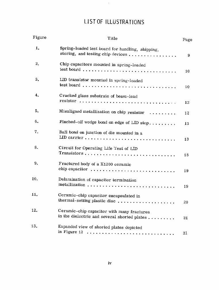
LIST OF ILLUSTRATIONS
Figure Title Page
1. Spring-loaded test board for handling, shipping,storing, and testing chip devices ................ 9
2. Chip capacitors mounted in spring-loadedtest board .............................. . 10
3. LID transistor mounted in spring-loadedtest board . . . . . . . . . . . . . . . . . .. ............ 10
4. Cracked glass substrate of beam-leadresistor ................................ 12
5. Misaligned metallization on chip resistor ......... 12
6. Pinched-off wedge bond on edge of LID step ......... 13
7. Ball bond on junction of die mounted in aLID carrier ............................. 13
8. Circuit for Operating Life Test of LIDTransistors .............................. 18
9. Fractured body of a K1200 ceramicchip capacitor . . . . . . . . . . . . . . . . . ......... 19
10. Delamination of capacitor terminationmetallization . . . . . . . . . . . . . . . . . . . . . . ..... 19
11. Ceramic-chip capacitor encapsulated in
thermal-setting plastic disc ................... 20
12. Ceramic-chip capacitor with many fracturesin the dielectric and several shorted plates ......... 21
13. Expanded view of shorted plates depictedin Figure 12 ............................. 21
iv

LIST OF ILLUSTRATIONS (Concluded)
Figure Title Page
14. Ceramic-chip capacitor with plate failing tocontact termination metallization .22
15. Peppered effect of abrasive trimmedchip resistors . ............................. 22
16. Microcracks in laser trimmed chip resistors .2... 23
17. Lifted bond on chip transistor ................... 23
v

LI ST OF TABLES
Table Title Page
1. Qualification Tests for Ceramic Capacitors ........ 4
2. Qualification Tests for TantalumCapacitors .............................. 5
3. Qualification Tests for Resistors ............... 5
4. Qualification Tests for Transistors ............. 6
5. Screening Tests for Ceramic Capacitors .......... 7
6. Screening Tests for TantalumCapacitors .............................. 8
7. Screening Tests for Resistors ................. 8
8. Screening Tests for Transistors ............... 8
9. Reliability Tests Performed forFailure Analysis Studies of DiscreteC omponents ............................. 14
10. Ratio Failure Rates for Capacitors Subjectedto Temperature Coefficient Tests . ............ 15
11. Reliability Data Summary for CapacitorsSubjected to Operating Life Tests at125'C and Rated Voltage ..................... 15
12. Ratio Failure Rates for Resistors Subjectedto Temperature Coefficient Tests .............. 16
13. Reliability Data Summary for ResistorsSubjected to Operating Life Tests at 125'Cand Rated Power .......................... 17
14. Reliability Data Summary for TransistorsSubjected to Operating Life Tests .............. 17
vi

ACKNOWLEDGMENT
The authors gratefully acknowledge the efforts of Messrs. Monroe Yongueand Johnny Farner in bonding and mounting the components tested. Also, theauthors wish to thank Mr. Steve Graff for his dedication in performing thetests described and compiling the data. The authors express appreciation toMr. David Nicolas for his contributions in performing the scanning electronmicroscope investigations.
vii

TECHNICAL MEMORANDUM X- 64686
RELIABILITY OF HYBRID MICROCIRCUITDISCRETE COMPONENTS
INTRODUCTION
.The rapid acceptance of hybrid microcircuits as a major contributorto electronic system integration has created many problems in defining anddescribing accurate. reliability factors. The reliability of hybrid microcircuitsis determined by factors such as wire bonding, interconnection techniques,thick- and thin-film processing, discrete component mounting, and hermeticsealing. These factors can be controlled and regulated during fabricationcycles with proper process controls. However, the discrete component, overwhich the hybrid manufacturer exercises little or no control, poses the mostdominating effect on microcircuit reliability. With this consideration, eachhybrid manufacturer must establish criteria for selection, qualification, andscreening of discrete devices.
The Marshall Space Flight Center (MSFC) conducts inhouse researchand development in hybrid technology and fabricates prototype microcircuitsfor feasibility studies. The hybrid facility performs inhouse evaluations ofmicrocircuit discrete components. Results of these evaluations are distributedto hybrid manufacturers under NASA contract and NASA systems groups to useas guidelines in the design and specification of hybrid systems. Results ofmicrocircuit discrete component evaluations accumulated over several years ofstudy are summarized in this report.
HYBRID PROBLEMS
To list and discuss all the problems encountered in the fabrication anduse of hybrid microcircuits would be difficult, but this does not imply thathybrids are less reliable than other assembly methods. On the contrary,when microcircuitry is required, hybrids are definitely more advantageousand reliable to use than most assembly methods. The trends at MSFC and inindustry indicate that hybrids are gaining in popularity and usage. Generally,these microcircuits are produced in relatively small volume with a high degree
I
of sophistication. Only a few companies have experienced millions of manhoursin reliability testing and volume production of hybrids. Because of this lowvolume production and circuit specialization, hybrid microcircuits are cur-rently higher cost items than conventional electronics. However, this costfactor will improve as the technology develops and usage increases. Goodquality control and product assurance, selection of proper fabrication andassembly techniques, and close surveillance will ensure a good reliable prod-uct; i. e., problems can be virtually eliminated in such areas as film defects,contamination, bond failure, parts mounting, and package sealing by usinggood production control methods with complete and practical documentation.However, one phase of hybrid microcircuit technology is causing the mostconcern and problems in relation to circuit reliability; i. e., the basic control-ling factor in the reliability of hybrids is the quality of discrete parts used inthe circuit. Because of this, our policy has been to recommend and applyscreening procedures to every discrete component before assembly onto thesubstrate whenever long-life and high-reliability circuits are specified. Natu-rally, this can be a difficult and costly operation, especially when one con-siders the more complex integrated circuit chips being used today in hybridassemblies.
DISCRETE COMPONENT QUALIFICATION AND SCREENING
Qualification and screening of discrete chip devices are necessary toassure maximum reliability of hybrid microcircuits. However, many problemsarise when attempts are made to qualify and screen these devices. Amongthese problems are:
1. Determination of applicable specificatiols and standards.
2. Determination of meaningful test cond fions.
3. Fabrication of handling, storage, and test fixtures.
Marshall Space Flight Center attempts to guarantee reliability of discrete chipdevices through line certification. The method cannot be applied as a replace-ment for qualification and screening but is a valuable and necessarysupplement.
2
Line CertificationIn coordination with the Microelectronics Subcommittee of the NASA
Parts Steering Committee, MSFC has developed a program called line certifi-cation to improve reliability of microcircuits. The main feature of the linecertification program is based on the statistical control of key process steps.Work has been in progress for the past 7 years concerning monolithic micro-circuits. Documentation and procedures have recently been developed forhybrid microcircuit processing and is currently being tested on a trial-runbasis. The full monolithic-hybrid line certification program has beenoperational since June 1972.
The purpose of line certification is to raise the reliability level ofmicrocircuits and, more important,. to make this reliability more consistentto increase yield. For classification purposes, microcircuits are grouped intobroad categories such as monolithic and hybrid (others are planned). Experi-ence has been exclusively with monolithic manufacturing (semiconductor)facilities. First, upon the request of a supplier, an initial survey is con-ducted; then if sufficient microcircuits are being produced by a supplier inquantity and quality, an MSFC (or NASA-wide) team actually performs theline certification. The process usually requires three to four visits by theteam and may take 1 to 2 years to complete, depending upon the suppliers'facilities and process controls. It is anticipated that line certification will beperformed for hybrid microcircuits for pending procurement actions only.More details about the line certification program can be obtained from MSFC' sQuality and Reliability Assurance Laboratory.
QualificationAt MSFC the following documents are used to reference most qualifi-
cation tests conducted on discrete chip devices.
1. MIL-STD-202D, Test Methods for Electronic and ElectricalComponent Parts.
2. MIL-STD-883, Test Methods for Microelectronics.
3. MIL-STD-750A, Test Methods for Semiconductor Devices.
4. MSFC Specification 85M03927, Discrete Chip Devices for HybridMicrocircuits.
3

However, these specifications have several shortcomings when applied tohybrid circuits. Among these are:
1. The specifications are often too general and frequently omit neces-sary test conditions.
2. Allowable percent changes and parameter variations are generallyomitted from the specifications and are rarely given in the detailed componentspecification sheet.
3. Conditions such as shock and vibration levels are designed forlarge massive discrete components and are meaningless for small discretechip devices.
Each discrete chip device required different qualification tests. Dis-crete chip devices are qualified by applying the tests and specifications givenin Tables 1 through 4.
TABLE 1. QUALIFICATION TESTS FOR CERAMIC CAPACITORS
4
Test Specification or Condition
Visual Examination MSFC 85M03927
Capacitance MSFC 85M03927
Dissipation Factor MSFC 85M03927
Insulation Resistance MSFC 85M03927
Dielectric Withstanding MSFC 85M03927Voltage
Temperature Coefficient MIL-STD-202D, Method 304
Operating Life MIL-STD-202D, Method 108ACondition D
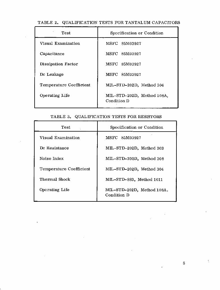
TABLE 2. QUALIFICATION TESTS FOR TANTALUM CAPACITORSI I.a
Test
Visual Examination
Capacitance
Dissipation Factor
Dc Leakage
Temperature Coefficient
Operating Life
Specification or Condition
MSFC 85M03927
MSFC 85M03927
MSFC 85M03927
MSFC 85M03927
MIL-STD-202D, Method 304
MIL-STD-202D, Method 108A,Condition D
TABLE 3. QUALIFICATION TESTS FOR RESISTORS
Test Specification or Condition
Visual Examination MSFC 85M03927
Dc Resistance MIL-STD-202D, Method 303
Noise Index MIL-STD-202D, Method 308
Temperature Coefficient MIL-STD-202D, Method 304
Thermal Shock MIL-STD-883, Method 1011
Operating Life MIL-STD-202D, Method.108A,Condition D
5

TABLE 4. QUALIFICATION TESTS FOR TRANSISTORS
Test Specification
Visual Examination MSFC 85M03927MIL-STD- 883, Method 2010
Electrical Measurements MSFC 85M03927MIL-STD- 750A
High Temperature and MSFC 85M03927Impressed Voltage
Temperature Cycling MIL-STD-883, Method 1010
Power Burn-in MSFC 85M039271000 hours at maximum rated power
ScreeningScreening, as applied to components for hybrid microcircuits, is the
testing of a discrete device before assembly into a circuit. This screeningmay consist of reading only one parameter but, nevertheless, every discretechip device is subjected to some type of pretesting.
At MSFC the most important factor controlling the reliability of hybridmicrocircuits is the discrete chip devices in the assembly. As previouslypointed out, problems with wire bonds, thin- and thick-film elements, con-tamination, and package sealing can be almost eliminated with good qualityand process control procedures. However, most hybrid manufacturers pur-chase practically all discrete chip devices and therefore have little controlover the manufacturing process. Regardless of the tight specification andscreening requirements to which discrete devices are procured, a failure rateof 10 to 40 percent is very likely. A hybrid assembly with several discretechip devices has a slight statistical chance of working properly withoutreplacement of one or more parts. More than 50 percent of all custom hybridassemblies are reworked or repaired at least once. The rework that isreferred to and considered detrimental to reliability is the removal andreplacement of discrete components.
6

Rework of hybrids is currently one of the most controversial problemsfacing the hybrid industry. Based on experience with inhouse programs andwith hardware manufactured by contract, some degradation has been observedin the reliability of a circuit once it has been reworked. The only way to avoidrework is 100 percent screening and power burn-in of discrete chips beforeattachment on the substrate. This is the policy adopted by MSFC when require-ments specify high reliability hybrid hardware. Since this policy requiresspecial equipment and procedures, less critical circuit applications may notrequire 100 percent burn-in of all devices. The screening tests for discretechip devices specified by the Hybrid Microcircuit Research Section are givenin Tables 5 through 8. These tests are performed on every chip device beforemounting into the hybrid as'sembly.
MSFC Approach. Screening can be done at various levels. For instance,screening can be performed where the device is manufactured or where thehybrid circuit is assembled. There are many different philosophies concern-ing the place where screening should be performed. However, AstrionicsLaboratory recommends that screening tests be performed where the hybridmicrocircuit is assembled because several problems have been traced to defec-tive chip devices that were supposedly screened at the factory. This methodsubstantially reduces the total cost of the discrete chip devices and creates anadditional confidence that no defective part will be assembled into the hybridmicrocircuit.
TABLE 5. SCREENING TESTS FOR CERAMIC CAPACITORS
7
Test Specification
Visual Examination MSFC 85M03927
Capacitance MSFC 85M03927
Dissipation Factor MSFC 85M03927
Insulation Resistance MSFC 85M03927
Dielectric Withstanding MSFC 85M03927Voltage
Power Burn-in MSFC 85M03927

TABLE 6. SCREENING TESTS FOR TANTALUM CAPACITORS
Test
Visual Examination
Capacitance
Dissipation Factor
Power Burn-in
Specification
MSFC 85M03927
MSFC 85M03927
MSFC 85M03927
MSFC 85M03927
TABLE 7. SCREENING TESTS FOR RESISTORS
Test Specification
Visual Examination MSFC 85M03927
Dc Resistance MIL-STD-202D, Method 303
Noise Index MIL-STD-202D, Method 308
Low Temperature MIL-R-55342Operation
Power Burn-in MSFC 85M03927
TABLE 8. SCREENING TESTS FOR TRANSISTORS
Test Specification
Visual Examination MSFC 85M03927
Electrical Measurements MSFC 85M03927
High Temperature and MSFC 85M03927Impressed Voltage
Power Burn-in MSFC 85M03927
8

Handling Problems. One of the problems with screening is the handling of the chip. Marshall Space Flight Center has developed and patented a spring-loaded test board for handling, shipping, storing, and testing chip devices. This includes chip resistors , chip capacitors, leadless inverted devices (LED), and beam-lead type transistors, diodes, and integrated circuits. With slight modifications, these test boards can be used for nearly all chip devices presently on the market. The basic test board, illustrated in Figure 1, is a single-sided rexolite printed wiring board. The chip devices are held in position with beryllium-copper springs soldered through the rexolite board to the gold-plated copper pattern. The use of these test boards in conjunction with simple fixturing for a multiburn-in station has greatly enhanced our ability to perform screening tests on discrete chip devices. At the present time, MSFC recommends that all semiconductor die requiring preassembly burn-in be procured mounted on ceramic carr iers , such as LID or U-channel packages. This facilitates the screening processes and handling during assembly. Figures 2 and 3 illustrate chip devices in the test fixtures.
Figure 1. Spring-loaded test board for handling, shipping, storing, and testing chip devices.
This page is reproduced at the back of the report by a different reproduction method to provide better detail.
9

Figure 2. Chip capacitors mounted in spring-loaded test board.
Figure 3. LID transistor mounted in spring-loaded test board.
This page is reproduced at the back of the report by a different reproduction method to provide better detail.
10

RESULTS OF FAILURE ANALYSIS STUDIES
Much test data on discrete chip devices have been accumulated overthe past several years. A general survey of the discrete chip industry revealsthat many of the chip devices fail to meet minimum MSFC screening and quali-fication specifications. Most of the chip devices sold today are designed forcommercial application and lack sufficient process documentation and trace-ability. This section details results of visual examinations, scanning electronmicroscope examinations, and screening and qualification test results.
Incoming Receiving Visual Examination
Two specifications are used by MSFC to control visual examinations ofmicrocircuit discrete devices: 85M03927, Discrete Chip Devices for HybridMicrocircuits and 85M03924, Internal Visual Inspection of SemiconductorDevices. When tested to these specifications, discrete devices often encoun-ter a fall-out rate of 10 to 30 percent. The primary causes of failure aremisalignment, false cuts, cracks, nicks, scratches, metallization defects,and defective wedge and ball bonds. Figures 4, 5, 6, and 7 illustrate typicalvisual failures. The only way to control and possibly eliminate these types offailures is to impose the specifications stated. However, because this oftenreflects an individual discrete device price increase, MSFC usually purchasesthe parts without the specifications imposed and performs the testing after theparts are received.
Electrical and Environmental Evaluation
This section reveals data of tests performed on capacitors, resistors,and bipolar transistors. Each device was compared using different tests.Table 9 depicts the various tests used to illustrate the results.
Methods of Statistical Analysis
Discussion of ratio failure rate. The ratio failure rate is the ratio ofthe number of failures which occur during a unit interval of time to the origi-nal number of parts at the start of the reliability test. This is given by the
fformula X =- , where X = ratio failure rate, f = total failures during
na given interval of time, and n = number of parts originally placed on test.
11
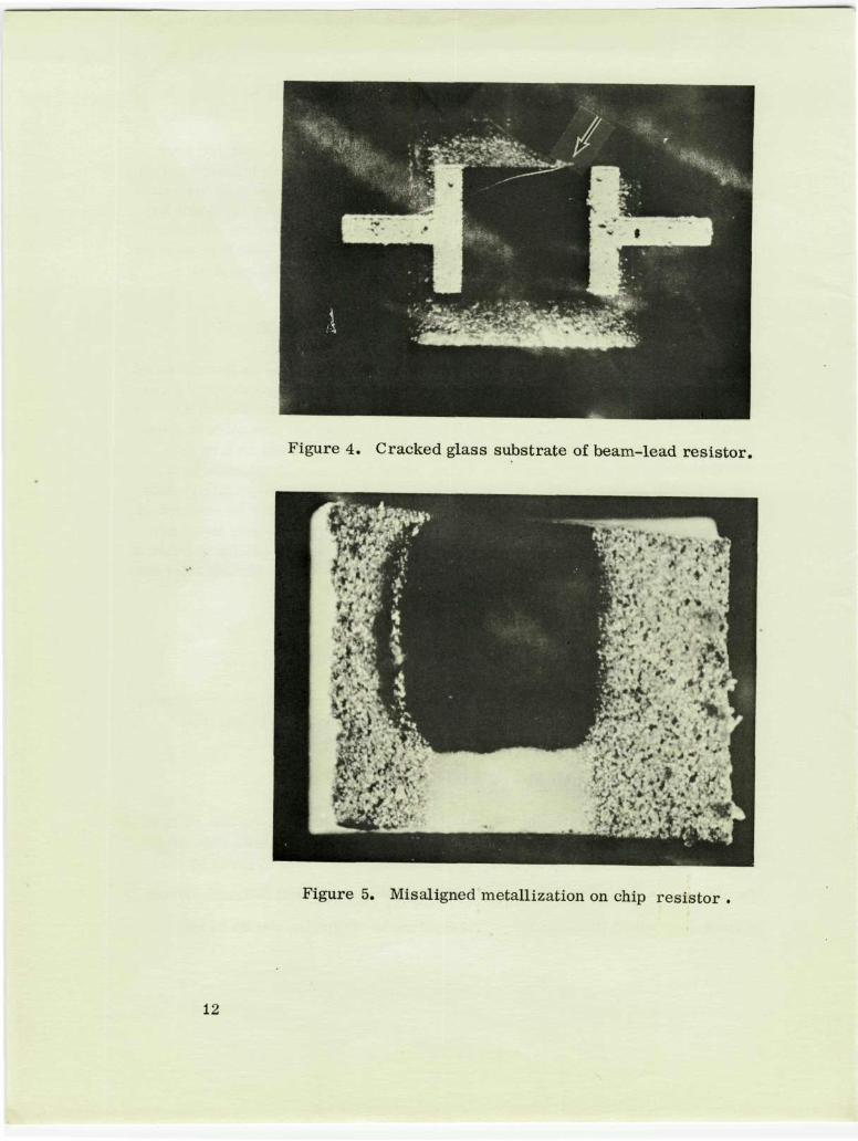
Figure 4. Cracked glass substrate of beam-lead resistor.
12
Figure 5. Misaligned metallization on chip resistor .

Figure 6. Pinched-off wedge bond on edge of LID s tep .
Figure 7. Ball bond on junction of die mounted in a LID c a r r i e r .
This page is reproduced at the back of the report by a different reproduction method to provide better detail.
13

TABLE 9. RELIABILITY TESTS PERFORMED FOR FAILURE ANALYSISSTUDIESOF DISCRETE COMPONENTS
The ratio failure rate is used to predict the probability of failure during aparticular time interval and is especially useful in that it gives the fraction oforiginal parts which are expected to survive during a particular time interval.
Discussion of failure rate. The failure rate, or hazard rate, isexpressed in terms of failures per unit of time. It is computed as a simpleratio of the number of failures during a specified test interval to the aggregatesurvival test time of the devices undergoing test during the test interval. The
fequation for this relationship is r T ,where r = failure rate per hour,
f = total number of failures for the test interval, and T = total test hours.This failure rate is used to predict the number of failures that will occurduring a particular time interval.
Mean time between failures. The mean time between failures (MTBF)is probably the most commonly used term to describe component reliability.It is computed by taking the reciprocal of the failure rate and is expressed inunits of time. As the term indicates, it is used to predict the mean timebetween failures for a component or circuit.
14
Component Type Tests Performed
Capacitors Temperature Coefficient(-55° C to 125 ° C)
Life (1000 hours, 1250 C,rated voltage)
Resistors Temperature Coefficient(-65° C to 150° C)
Life (1000 hours, 125°C,rated power)
Transistors Life (emitter loading,80 percent rated power)

Capacitors. Three types of capacitors are generally used in hybridmicrocircuits. These are barium-titanate ceramic chips, beam-lead tantalumchips, and solid-tantalum chips. The data given depict the test results of thebarium-titanate ceramic chip capacitors only. Tests on the beam-lead andsolid-tantalum types are in progress and will be reported at a later date.Tables 10 and 11 illustrate the data taken on these chip capacitors.
TABLE 10. RATIO FAILURE RATES FOR CAPACITORSSUBJECTED TO TEMPERATURE COEFFICIENT TESTS
TABLE 11. RELIABILITY DATA SUMMARY FOR CAPACITORSSUBJECTED TO OPERATING LIFE TESTS AT 1250 C
AND RATED VOLTAGE
15
Ratio FailureNumber Tested Number Failed Rate (percent)
56 44 78.6
90 2 2.2
128 22 17.2
66 56 84.8
180 41 22.8
Total RatioNumber Number Test Failure Failure
Vendor Tested Failed Hours Rate MT BF Rate
Per106 Hours\ Hours Percent
A 56 17 46 448 366 2740 30.4
B 150 9 306 000 29 34 014 6.0
C 128 6 261 120 23 43 478 4.7
D 56 2 114 240 18 57 143 3.6

For the data given in Table 9, a failure was defined as any capacitorthat failed to meet the specifications on the manufacturer' s data sheets.Typically, this was ±15 percent capacitance change over the temperaturerange -55' C to +1250 C for type K1200 and +30 ppm/o C for type negative-positive-zero (NPO).
For the data presented in Table 10, a failure was defined as any capac-itor that opened, shorted, had a capacitance change greater than +10 percent,had a dissipation factor greater than 10 percent, or had an insulation resist-ance less than 104 Mo or 100 Mp2 - /F , whichever is less.
Resistors. Three types of resistors were examined: thick-film, cer-met pellet, and tantalum nitride. Tables 12 and 13 illustrate the data takenfor temperature coefficient and operating life tests, respectively.
TABLE 12. RATIO FAILURE RATES FOR RESISTORSSUBJECTED TO TEMPERATURE COEFFICIENT TESTS
In Table 12, vendors A and B represent thick-film resistors, vendorC is a cermet-pellet resistor, and vendors D and E are tantalum-nitride resis-tors. In this table, a failure was defined as any resistor that failed to meetthe rated temperature coefficient of resistance specified on the manufacturer' sdata sheets. All resistors were tested over the temperature range of -55° Cto 125' C. Obviously, some of the high failure rates are merely the reflectionof manufacturers' exaggerated performance claims, and would appear as amore reliable resistor if the specification sheets reflected more realisticperformance claims.
In Table 13, vendors A and B are thick-film chip resistors, vendor Cis a cermet-pellet resistor, and vendor D is a tantalum-nitride resistor. For
16
Ratio FailureVendor Number Tested Number Failed Rate (percent)
A 32 1 3.1
B 60 2 3.3
C 160 16 10.0
D 96 23 24.0
E 100 2 2.0
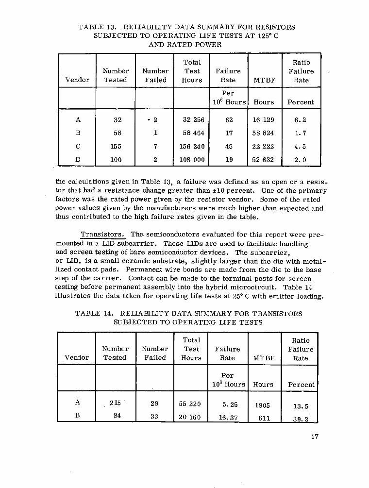
TABLE 13. RELIABILITY DATA SUMMARY FOR RESISTORSSUBJECTED TO OPERATING LIFE TESTS AT 1250 C
AND RATED POWER
Total RatioNumber Number Test Failure Failure
Vendor Tested Failed Hours Rate MTBF Rate
Per106 Hours Hours Percent
A 32 · 2 32 256 62 16 129 6.2
B 58 1 58 464 17 58 824 1.7
C 155 7 156 240 45 22 222 4.5
D 100 2 108 000 19 52 632 2.0
the calculations given in Table 13, a failure was defined as an open or a resis-tor that had a resistance change greater than ±10 percent. One of the primaryfactors was the rated power given by the resistor vendor. Some of the ratedpower values given by the manufacturers were much higher than expected andthus contributed to the high failure rates given in the table.
Transistors. The semiconductors evaluated for this report were pre-mounted in a LID subcarrier. These LIDs are used to facilitate handlingand screen testing of bare semiconductor devices. The subcarrier,or LID, is a small ceramic substrate, slightly larger than the die with metal-lized contact pads. Permanent wire bonds are made from the die to the basestep of the carrier. Contact can be made to the terminal posts for screentesting before permanent assembly into the hybrid microcircuit. Table 14illustrates the data taken for operating life tests at 25' C with emitter loading.
TABLE 14. RELIABILITY DATA SUMMARY FOR TRANSISTORSSUBJECTED TO OPERATING LIFE TESTS
Total RatioNumber Number Test Failure Failure
Vendor Tested Failed Hours Rate MTBF Rate
Per
106 Hours Hours Percent
A 215 ' 29 55 220 5.25 1905 13.5
B 84 33 20 160 16.37 611 39.3
17

For this calculation, a failure was defined as any part that opened,shorted, or had an hFE out of tolerance given by the manufacturer's rated
specification. Each of the transistors tested was loaded to 100 milliwattsat 25° C ambient with emitter loading. A diagram of this loading circuit isshown in Figure 8.
OUT VCC
V|| _ 8 | WE TEN I VCE x IEBE
T _
Figure 8. Circuit for Operating Life Test of LID Transistors.
The high failure rates for this device are characterized primarily bypoor workmanship which the manufacturer conveniently hides with epoxyencapsulant. Wherever possible, NASA recommends the LID transistors bepurchased without an epoxy encapsulant. Thus, the hybrid manufacturer canvisually examine the transistor die before assembly. It is believed that thismethod of application will greatly enhance hybrid circuit reliability by elimi-nating many potential transistor failures.
Optical Examination of Failed Devices. The Hybrid M'crocircuitResearch Section endeavors to classify a mode of failure for eac? failed device.In this effort, the evaluations performed serve their greatest purpose to boththe discrete chip device vendor and the hybrid manufacturer. Optical exami-nations can be used to identify most of the modes of failure. Typical failuremodes described by optical examination are illustrated in Figures 9 and 10.
18
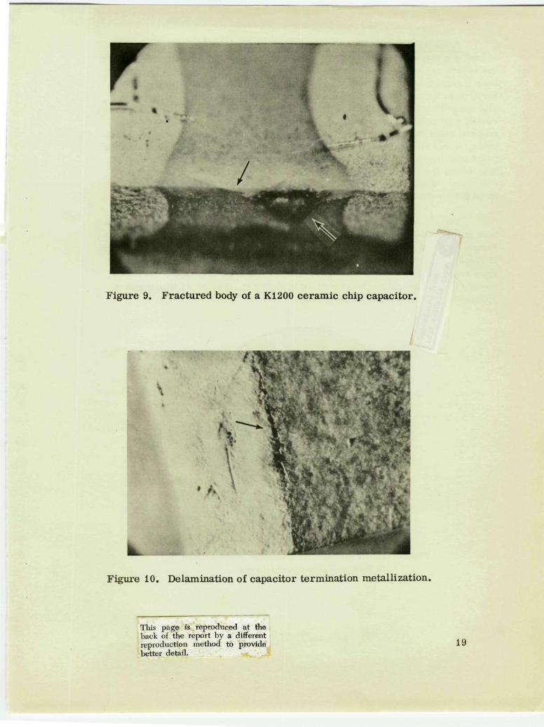
Figure 9. Fractured body of a K1200 ceramic chip capacitor.
Figure 10. Delamination of capacitor termination metallization.
This page is reproduced at the back of the report by a different reproduction method to provide better detail.

Scanning Electron Microscope Examinations of Failed Devices. Thescanning electron microscope (SEM) has been a principal investigative tool inthe failure analysis of discrete chip devices. All types of chip devices havebeen investigated, including ceramic-chip capacitors, chip resistors, andsemiconductors. The electron microscope is employed primarily becausehigh magnification optics have a definite limited depth of field. The SEMemploys an electron beam which is focused to a submicron sized spot on aninclined plane specimen. These include reflected electrons, secondary elec-trons, X-ray fluorescence, and cathode luminescence. Synchronized with thebeam spot position of the substrate, these signals are put into a cathode-raytube where they provide a high resolution image of that particular surfaceemission. Depth of field of the SEM permits formation of high quality imagesat 10 000x with excellent resolution.
The SEM examination process is characterized by mounting the speci-men in thermal-setting plastic. The plastic is then lapped and polished toexpose the area of failure. Once the area of failure is revealed, the specimenis placed in the SEM and SEMographs are prepared. Often large ceramicspecimens require a i to 2 picometer (100 to 200 angstrom units) goldcoating to prevent charge buildup while in the SEM. Figure ii illustrates aspecimen in the thermal-setting plastic.
Figure 11. Ceramic-chip capacitor encapsulatedin thermal-setting plastic disc.
20

The most significant findings using the SEM are ( l ) capacitor-plate s t ruc ture (F igs . 12, 13, and 14); (2) peppered effect on abrasive t r immed chip r e s i s t o r s (Fig . 15) ; (3) mic rocracks in l a se r - t r immed chip r e s i s t o r s (Fig. 16) ; and (4) lifted ball bond on a chip t rans is tor (Fig. 17). The capacitor with shorted plates , i l lustrated in Figures 12 and 13, had no physical external damage when observed optically at lOOx and visually appeared to be in perfect operating condition. The short is caused by a porous dielectr ic and occurred at 168 hours of life tes t at 125*C.
Figure 12. Ceramic-chip capacitor with many fractures in the dielectr ic and severa l shorted pla tes .
Figure 13. Expanded view of shorted plates depicted in Figure 12.
This page is reproduced at the back of the report by a different reproduction method to provide better detail.
c

Figure 14. Ceramic-chip capacitor with plate failing to contact termination metallization.
Figure 15. Peppered effect of abrasive trimmed chip resistors.
This page is reproduced at the back of the report by a different reproduction method to provide better detail.
22

Figure 16. Microcracks in laser trimmed chip resistors.
Figure 17. Lifted bond on chip transistor.
This page is reproduced at the back of the report by a different reproduction method to provide better detail.
23

CONCLUSIONS
The test results clearly demonstrate that the discrete component isthe most critical part in the hybrid microcircuit. Also, the data illustrate avaried difference in component vendor and type of component. To design thebest quality component into the hybrid microcircuit at the most economicalprice, the hybrid manufacturer must have a thorough working knowledge ofthe application of his discrete components and he must understand their per-formance capability and limitations.
The data clearly illustrate that semiconductors have the highest rejec-tion rate of all discrete components. All of the semiconductors tested wereLIDs supplied with an epoxy encapsulant. A cross section of one of the failedsemiconductors revealed multiple bond attempts on the LID base surface.Marshall Space Flight Center concludes that the epoxy encapsulant merelyhides poor workmanship and thus believes a more reliable part can be suppliedwhen no epoxy encapsulant is used. This affords the hybrid manufacturer theopportunity to visually inspect the die and the wire bonds. However, it mustbe noted that extra care in handling must be given to unencapsulated devices.Also, the unencapsulated devices do not dissipate as much power as thosewith the epoxy encapsulant.
Close analysis of the data verifies that all discrete components inaerospace high-reliability systems should undergo some screening and burn-in before assembly application. The screening requirements given in Tables5, 6, 7, and 8 are recommended by MSFC. Also, MFSC recommends that allsemiconductors, excluding beam-lead devices, requiring preassembly burn-in be procured mounted on some type of ceramic carrier.
A multiplexer system currently in assembly at MSFC is comprised ofover 140 digital integrated circuits in the die form. These dies were orderedto the precap visual inspection of MIL-STD-883, Method 2010, Condition B.When assembled in the hybrid circuits, over 75 percent of all devices hadsome failures and required repair or replacement. Marshall Space FlightCenter contends that procurement of these devices on a carrier would havefacilitated power burn-in and greatly reduced the repair and rework required.Since repair and rework of hybrid circuits is discouraged and often not per-mitted by MSFC for high-reliability long term missions, it is believed thata cost savings is realized when the devices undergo preassembly power burn-in.
24
FUTURE PROGRAMS
The failure analysis studies presented are merely a segment of a con-tinuous program. Future work will include evaluation of beam-lead compon-ents, microwave porcelain capacitors, and power devices. Also, new vendorswill be evaluated along with reevaulation of vendors already tested.
Other programs will include improving the existing design of the burn-in test carriers, illustrated in Figure 1, and design of a burn-in test carrierfor power devices. Furthermore, if the use of active chips in the die form ispermitted, meaningful screening programs must be developed.
25
APPROVAL TM X- 64686
RELIAB ILTY OF HYBRID MI CROCIRCU ITD i SCRETE COMPONENTS
By Robert V. Allen and Salvadore V. Caruso
The information in this report has been reviewed for security classifi-cation. Review of any information concerning Department of Defense or AtomicEnergy Commission programs has been made by the MSFC Security Classifica-tion Officer. This report, in its entirety, has been determined to be unclassi-fied.
This document has also been reviewed and approved for technicalaccuracy.
D. L. ANDERSONChief, Microelectronics Branch
C. TAYLORChief, Technology Division
3,. \sta,
26
F.B. MOOREDirector, Astrionics Laboratory