general-purpose otp mcu with 14 i/o lines ... - rs...
TRANSCRIPT
ZiLOG Worldwide Headquarters • 910 E. Hamilton Avenue • Campbell, CA 95008Telephone: 408.558.8500 • Fax: 408.558.8300 • www.ZiLOG.com
PS004602-0401
PRELIMINARY
Product Specification
Z86E02/E04/E08/E09
General-Purpose OTP MCU with 14 I/O LInes
P R E L I M I N A R Y
PS004602-0401
This publication is subject to replacement by a later edition. To determine whether a later edition exists, or to request copies of publications, contact:
ZiLOG Worldwide Headquarters
910 E. Hamilton AvenueCampbell, CA 95008Telephone: 408.558.8500Fax: 408.558.8300www.ZiLOG.com
ZiLOG is a registered trademark of ZiLOG Inc. in the United States and in other countries. All other products and/or service names mentioned herein may be trademarks of the companies with which they are associated.
Document Disclaimer
© 2001 by ZiLOG, Inc. All rights reserved. Information in this publication concerning the devices, applications, or technology described is intended to suggest possible uses and may be superseded. ZiLOG, INC. DOES NOT ASSUME LIABILITY FOR OR PROVIDE A REPRESENTATION OF ACCURACY OF THE INFORMATION, DEVICES, OR TECHNOLOGY DESCRIBED IN THIS DOCUMENT. ZiLOG ALSO DOES NOT ASSUME LIABILITY FOR INTELLECTUAL PROPERTY INFRINGEMENT RELATED IN ANY MANNER TO USE OF INFORMATION, DEVICES, OR TECHNOLOGY DESCRIBED HEREIN OR OTHERWISE. Except with the express written approval ZiLOG, use of information, devices, or technology as critical components of life support systems is not authorized. No licenses or other rights are conveyed, implicitly or otherwise, by this document under any intellectual property rights.
Z86E02/E04/E08/E09General-Purpose OTP MCU with 14 I/O LInes
iii
Table of Contents
Architectural Overview . . . . . . . . . . . . . . . . . . . . . . . . . . . . . . . . . . . . . . . . . 1Z86E02/E04/E08/E09 SL1995 Features . . . . . . . . . . . . . . . . . . . . . . . . . 1
Block Diagrams . . . . . . . . . . . . . . . . . . . . . . . . . . . . . . . . . . . . . . . . . . . . . . . 3Pin Description . . . . . . . . . . . . . . . . . . . . . . . . . . . . . . . . . . . . . . . . . . . . . . . 5Electrical Characteristics . . . . . . . . . . . . . . . . . . . . . . . . . . . . . . . . . . . . . . . 12
Absolute Maximum Ratings . . . . . . . . . . . . . . . . . . . . . . . . . . . . . . . . . . 12Standard Test Conditions . . . . . . . . . . . . . . . . . . . . . . . . . . . . . . . . . . . 13Capacitance . . . . . . . . . . . . . . . . . . . . . . . . . . . . . . . . . . . . . . . . . . . . . . 13
DC Electrical Characteristics . . . . . . . . . . . . . . . . . . . . . . . . . . . . . . . . . . . . 14AC Electrical Timing Characteristics . . . . . . . . . . . . . . . . . . . . . . . . . . . . . . 25
Low-Noise Version . . . . . . . . . . . . . . . . . . . . . . . . . . . . . . . . . . . . . . . . 31Pin Functions . . . . . . . . . . . . . . . . . . . . . . . . . . . . . . . . . . . . . . . . . . . . . . . . 32
EPROM Mode . . . . . . . . . . . . . . . . . . . . . . . . . . . . . . . . . . . . . . . . . . . . 32STANDARD Mode . . . . . . . . . . . . . . . . . . . . . . . . . . . . . . . . . . . . . . . . . 32
Functional Description . . . . . . . . . . . . . . . . . . . . . . . . . . . . . . . . . . . . . . . . . 37RESET . . . . . . . . . . . . . . . . . . . . . . . . . . . . . . . . . . . . . . . . . . . . . . . . . . 37Program Memory . . . . . . . . . . . . . . . . . . . . . . . . . . . . . . . . . . . . . . . . . . 39Register File . . . . . . . . . . . . . . . . . . . . . . . . . . . . . . . . . . . . . . . . . . . . . 40Stack Pointer . . . . . . . . . . . . . . . . . . . . . . . . . . . . . . . . . . . . . . . . . . . . . 42General-Purpose Registers . . . . . . . . . . . . . . . . . . . . . . . . . . . . . . . . . 42Counter/Timer . . . . . . . . . . . . . . . . . . . . . . . . . . . . . . . . . . . . . . . . . . . . 42Interrupts . . . . . . . . . . . . . . . . . . . . . . . . . . . . . . . . . . . . . . . . . . . . . . . . 43Clock . . . . . . . . . . . . . . . . . . . . . . . . . . . . . . . . . . . . . . . . . . . . . . . . . . . 45HALT Mode . . . . . . . . . . . . . . . . . . . . . . . . . . . . . . . . . . . . . . . . . . . . . . 46STOP Mode . . . . . . . . . . . . . . . . . . . . . . . . . . . . . . . . . . . . . . . . . . . . . . 47Watch-Dog Timer . . . . . . . . . . . . . . . . . . . . . . . . . . . . . . . . . . . . . . . . . 48Auto Reset Voltage . . . . . . . . . . . . . . . . . . . . . . . . . . . . . . . . . . . . . . . . 48
OTP Option Bit Description . . . . . . . . . . . . . . . . . . . . . . . . . . . . . . . . . . . . . 50Control Registers . . . . . . . . . . . . . . . . . . . . . . . . . . . . . . . . . . . . . . . . . . . . . 51Package Information . . . . . . . . . . . . . . . . . . . . . . . . . . . . . . . . . . . . . . . . . . 59Ordering Information . . . . . . . . . . . . . . . . . . . . . . . . . . . . . . . . . . . . . . . . . . 61
Part Number Description . . . . . . . . . . . . . . . . . . . . . . . . . . . . . . . . . . . . 62Special Lot 1995 . . . . . . . . . . . . . . . . . . . . . . . . . . . . . . . . . . . . . . . . . . 62Precharacterization Product . . . . . . . . . . . . . . . . . . . . . . . . . . . . . . . . . 62
Document Information . . . . . . . . . . . . . . . . . . . . . . . . . . . . . . . . . . . . . . . . . 63Document Number Description . . . . . . . . . . . . . . . . . . . . . . . . . . . . . . . 63Change Log . . . . . . . . . . . . . . . . . . . . . . . . . . . . . . . . . . . . . . . . . . . . . . 63
PS004602-0401 P R E L I M I N A R Y Table of Contents
Z86E02/E04/E08/E09General-Purpose OTP MCU with 14 I/O LInes
iv
Index . . . . . . . . . . . . . . . . . . . . . . . . . . . . . . . . . . . . . . . . . . . . . . . . . . . . . . 64Customer Feedback Form . . . . . . . . . . . . . . . . . . . . . . . . . . . . . . . . . . . . . . 63
PS004602-0401 P R E L I M I N A R Y Table of Contents
Z86E02/E04/E08/E09General-Purpose OTP MCU with 14 I/O LInes
PS004602-0401 P R E L I M I N A R Y List of Figures
v
List of Figures
Figure 1. Functional Block Diagram . . . . . . . . . . . . . . . . . . . . . . . . . . . . . . . . . 3Figure 2. EPROM Programming Mode Block Diagram . . . . . . . . . . . . . . . . . . . 4Figure 3. 18-Pin DIP/SOIC Configuration, STANDARD Mode . . . . . . . . . . . . . 5Figure 4. 18-Pin DIP/SOIC Configuration, EPROM Mode . . . . . . . . . . . . . . . . 7Figure 5. 20-Pin SSOP Pin Configuration, STANDARD Mode . . . . . . . . . . . . . 8Figure 6. 20-Pin SSOP Pin Configuration, EPROM Mode . . . . . . . . . . . . . . . 10Figure 7. Test Load Diagram . . . . . . . . . . . . . . . . . . . . . . . . . . . . . . . . . . . . . 13Figure 8. AC Electrical Timing . . . . . . . . . . . . . . . . . . . . . . . . . . . . . . . . . . . . 25Figure 9. Port 0 Configuration . . . . . . . . . . . . . . . . . . . . . . . . . . . . . . . . . . . . . 33Figure 10. Port 2 Configuration . . . . . . . . . . . . . . . . . . . . . . . . . . . . . . . . . . . . . 34Figure 11. Port 3 Configuration . . . . . . . . . . . . . . . . . . . . . . . . . . . . . . . . . . . . . 35Figure 12. Internal Reset Configuration . . . . . . . . . . . . . . . . . . . . . . . . . . . . . . 37Figure 13. Program Memory Map . . . . . . . . . . . . . . . . . . . . . . . . . . . . . . . . . . . 39Figure 14. Register File . . . . . . . . . . . . . . . . . . . . . . . . . . . . . . . . . . . . . . . . . . . 40Figure 15. Register Pointer . . . . . . . . . . . . . . . . . . . . . . . . . . . . . . . . . . . . . . . . 41Figure 16. Counter/Timers Block Diagram . . . . . . . . . . . . . . . . . . . . . . . . . . . . 43Figure 17. Interrupt Block Diagram . . . . . . . . . . . . . . . . . . . . . . . . . . . . . . . . . . 44Figure 18. Oscillator Configuration . . . . . . . . . . . . . . . . . . . . . . . . . . . . . . . . . . 45Figure 19. Typical Auto Reset Voltage vs. Temperature . . . . . . . . . . . . . . . . . 49Figure 20. 18-Pin DIP Package Diagram . . . . . . . . . . . . . . . . . . . . . . . . . . . . . 59Figure 21. 18-Pin SOIC Package Diagram . . . . . . . . . . . . . . . . . . . . . . . . . . . . 59Figure 22. 20-Pin SSOP Package Diagram . . . . . . . . . . . . . . . . . . . . . . . . . . . 60

Z86E02/E04/E08/E09General-Purpose OTP MCU with 14 I/O LInes
PS004602-0401 P R E L I M I N A R Y
vi
List of Tables
Table 1. Z86E02/E04/E08/E09 SL1995 Features . . . . . . . . . . . . . . . . . . . . . . . . 1Table 2. 18-Pin DIP/SOIC Pin Identification, STANDARD Mode . . . . . . . . . . . . . 5Table 3. 18-Pin DIP/SOIC Pin Identification, EPROM Mode . . . . . . . . . . . . . . . . 7Table 4. 20-Pin SSOP Pin Identification, STANDARD Mode. . . . . . . . . . . . . . . . 8Table 5. 18-Pin DIP/SOIC Pin Identification, EPROM Mode . . . . . . . . . . . . . . . 10Table 6. Absolute Maximum Ratings . . . . . . . . . . . . . . . . . . . . . . . . . . . . . . . . . 12Table 7. Capacitance . . . . . . . . . . . . . . . . . . . . . . . . . . . . . . . . . . . . . . . . . . . . . 13Table 8. DC Characteristics, Standard Temperature Range . . . . . . . . . . . . . . . 14Table 9. DC Characteristics, Extended Temperature Range . . . . . . . . . . . . . . . 19Table 10. AC Electrical Characteristics—STANDARD Mode and Temperature 26Table 11. AC Electrical Timing—STANDARD Mode at Extended Temperature 27Table 12. AC Electrical Timing—LOW NOISE Mode at Standard Temperature 28Table 13. AC Electrical Timing—LOW NOISE Mode at Extended Temperature 30Table 14. Z8 Control Registers Reset Values*. . . . . . . . . . . . . . . . . . . . . . . . . . 38Table 15. Interrupt Types, Sources, and Vectors. . . . . . . . . . . . . . . . . . . . . . . . 44Table 16. Typical Frequency vs. RC Values—VCC = 5.0 V @ 25°C. . . . . . . . . 45Table 17. Typical Frequency vs. RC Values—VCC
= 3.3 V @ 25°C. . . . . . . . . 46Table 18. Timer Mode Register . . . . . . . . . . . . . . . . . . . . . . . . . . . . . . . . . . . . . 51Table 19. Prescaler 1 Register. . . . . . . . . . . . . . . . . . . . . . . . . . . . . . . . . . . . . . 52Table 20. Counter/Timer 1 Register . . . . . . . . . . . . . . . . . . . . . . . . . . . . . . . . . . 52Table 21. Prescaler 0 Register. . . . . . . . . . . . . . . . . . . . . . . . . . . . . . . . . . . . . . 53Table 22. Port 2 Mode Register . . . . . . . . . . . . . . . . . . . . . . . . . . . . . . . . . . . . . 53Table 23. Counter/Timer 0 Register . . . . . . . . . . . . . . . . . . . . . . . . . . . . . . . . . . 53Table 24. Port 0 and 1 Mode Register . . . . . . . . . . . . . . . . . . . . . . . . . . . . . . . . 54Table 25. Port 3 Mode Register . . . . . . . . . . . . . . . . . . . . . . . . . . . . . . . . . . . . . 54Table 26. Interrupt Priority Register . . . . . . . . . . . . . . . . . . . . . . . . . . . . . . . . . . 55Table 27. Interrupt Request Register . . . . . . . . . . . . . . . . . . . . . . . . . . . . . . . . . 56Table 28. Flag Register . . . . . . . . . . . . . . . . . . . . . . . . . . . . . . . . . . . . . . . . . . . 57Table 29. Interrupt Mask Register . . . . . . . . . . . . . . . . . . . . . . . . . . . . . . . . . . . 57Table 30. General Purpose Register . . . . . . . . . . . . . . . . . . . . . . . . . . . . . . . . . 58Table 31. Stack Pointer Low . . . . . . . . . . . . . . . . . . . . . . . . . . . . . . . . . . . . . . . 58Table 32. Register Pointer . . . . . . . . . . . . . . . . . . . . . . . . . . . . . . . . . . . . . . . . . 58Table 33. Ordering Information . . . . . . . . . . . . . . . . . . . . . . . . . . . . . . . . . . . . . 61
Z86E02/E04/E08/E09General-Purpose OTP MCU with 14 I/O LInes
1
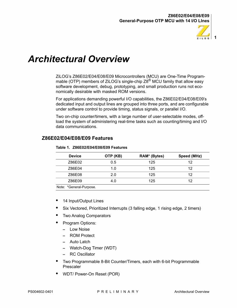
Architectural Overview
ZiLOG’s Z86E02/E04/E08/E09 Microcontrollers (MCU) are One-Time Program-mable (OTP) members of ZiLOG’s single-chip Z8® MCU family that allow easy software development, debug, prototyping, and small production runs not eco-nomically desirable with masked ROM versions.
For applications demanding powerful I/O capabilities, the Z86E02/E04/E08/E09’s dedicated input and output lines are grouped into three ports, and are configurable under software control to provide timing, status signals, or parallel I/O.
Two on-chip counter/timers, with a large number of user-selectable modes, off-load the system of administering real-time tasks such as counting/timing and I/O data communications.
Z86E02/E04/E08/E09 Features
• 14 Input/Output Lines
• Six Vectored, Prioritized Interrupts (3 falling edge, 1 rising edge, 2 timers)
• Two Analog Comparators
• Program Options:
– Low Noise
– ROM Protect
– Auto Latch
– Watch-Dog Timer (WDT)
– RC Oscillator
• Two Programmable 8-Bit Counter/Timers, each with 6-bit Programmable Prescaler
• WDT/ Power-On Reset (POR)
Table 1. Z86E02/E04/E08/E09 Features
Device OTP (KB) RAM* (Bytes) Speed (MHz)
Z86E02 0.5 125 12
Z86E04 1.0 125 12
Z86E08 2.0 125 12
Z86E09 4.0 125 12
Note: *General-Purpose.
PS004602-0401 P R E L I M I N A R Y Architectural Overview

Z86E02/E04/E08/E09General-Purpose OTP MCU with 14 I/O LInes
2
• On-Chip Oscillator that accepts Crystal, Ceramic Resonance, LC, RC, or External Clock
• Clock-Free WDT Reset
• Low-Power Consumption (50mW typical)
• Fast Instruction Pointer (1µs @ 12 MHz)
• RAM Bytes (125)
All Signals with an overline, “ ”, are active Low, for example:B/W (WORD is active Low); B/W (BYTE is active Low, only).
Power connections follow conventional descriptions, as noted below:
Connection Circuit Device
Power VCC VDD
Ground GND VSS
Note:
PS004602-0401 P R E L I M I N A R Y Architectural Overview
Z86E02/E04/E08/E09General-Purpose OTP MCU with 14 I/O LInes
3
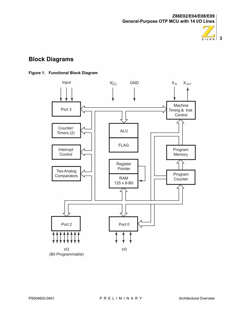
Block Diagrams
Figure 1. Functional Block Diagram
Port 3
Counter/Timers (2)
InterruptControl
Two AnalogComparators
Port 2
I/O(Bit Programmable)
ALU
FLAG
RegisterPointer
RAM125 x 8-Bit
Machine Timing & Inst.
Control
ProgramMemory
ProgramCounter
V GND XVInput
Port 0
I/O
CC OUTXIN
PS004602-0401 P R E L I M I N A R Y Architectural Overview
Z86E02/E04/E08/E09General-Purpose OTP MCU with 14 I/O LInes
4
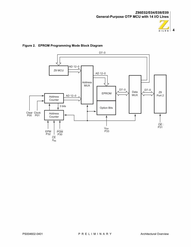
Figure 2. EPROM Programming Mode Block Diagram
AddressMUX
EPROM
Option Bits
AD 12–0
AD 12–0
Z8 MCU
EPMP32
D7–0 D7–0
AD 12–0
OEP31V
P33
D7–0
ClearP00
ClockP01
3 bits
PGMP30
CEX
Z8Port 2Address
Counter
AddressCounter
DataMUX
PP
IN
PS004602-0401 P R E L I M I N A R Y Architectural Overview
Z86E02/E04/E08/E09General-Purpose OTP MCU with 14 I/O LInes
5
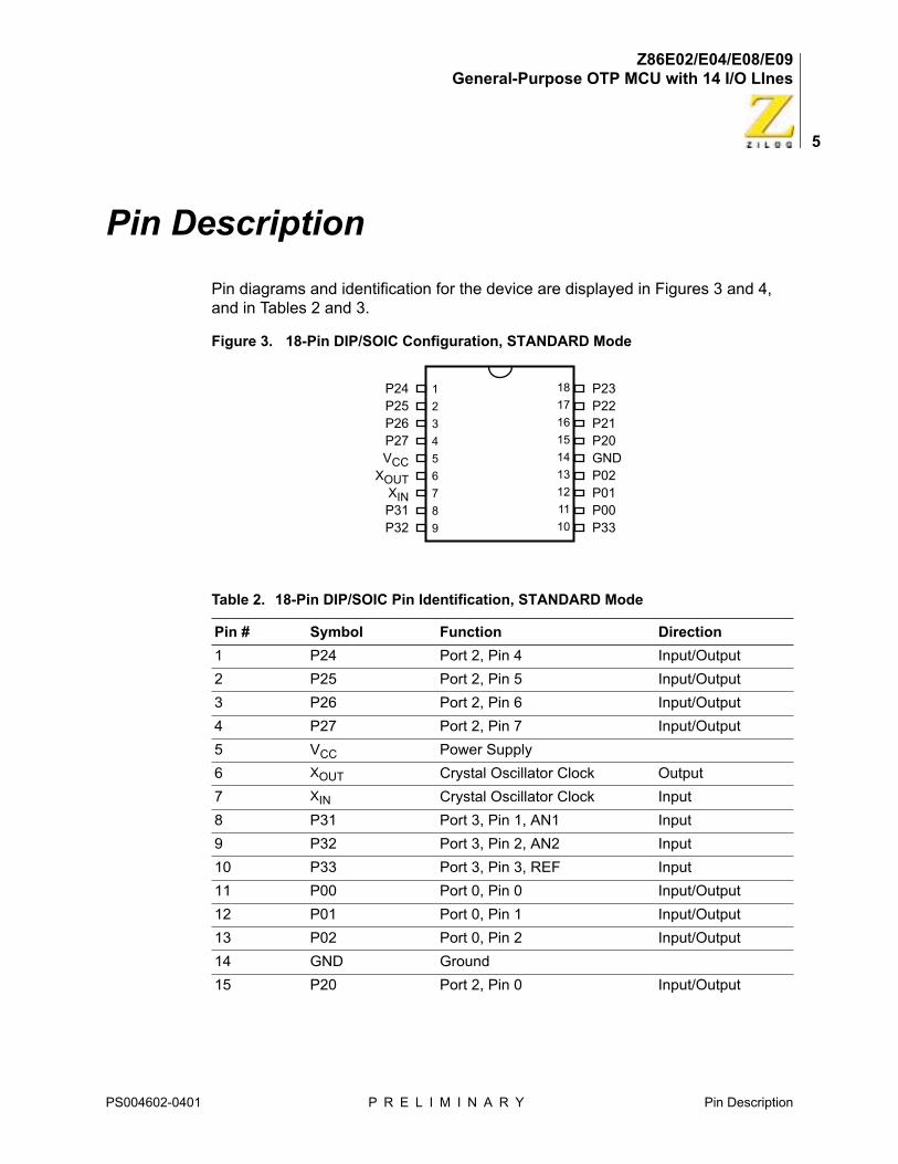
Pin Description
Pin diagrams and identification for the device are displayed in Figures 3 and 4, and in Tables 2 and 3.
Figure 3. 18-Pin DIP/SOIC Configuration, STANDARD Mode
Table 2. 18-Pin DIP/SOIC Pin Identification, STANDARD Mode
Pin # Symbol Function Direction
1 P24 Port 2, Pin 4 Input/Output
2 P25 Port 2, Pin 5 Input/Output
3 P26 Port 2, Pin 6 Input/Output
4 P27 Port 2, Pin 7 Input/Output
5 VCC Power Supply
6 XOUT Crystal Oscillator Clock Output
7 XIN Crystal Oscillator Clock Input
8 P31 Port 3, Pin 1, AN1 Input
9 P32 Port 3, Pin 2, AN2 Input
10 P33 Port 3, Pin 3, REF Input
11 P00 Port 0, Pin 0 Input/Output
12 P01 Port 0, Pin 1 Input/Output
13 P02 Port 0, Pin 2 Input/Output
14 GND Ground
15 P20 Port 2, Pin 0 Input/Output
P24P25P26P27VCC
XOUTXINP31P32
P23P22P21P20GNDP02P01P00P33
18
17
16
15
14
13
12
11
10
1
2
3
4
5
6
7
8
9
PS004602-0401 P R E L I M I N A R Y Pin Description
Z86E02/E04/E08/E09General-Purpose OTP MCU with 14 I/O LInes
6
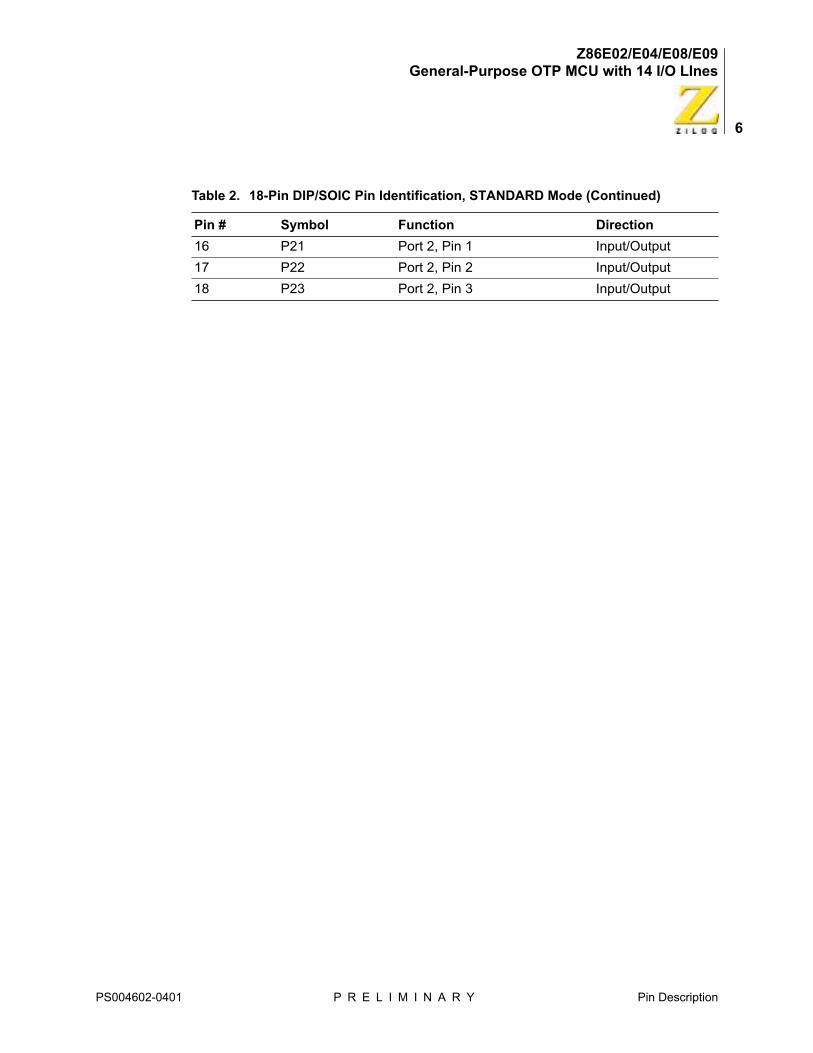
16 P21 Port 2, Pin 1 Input/Output
17 P22 Port 2, Pin 2 Input/Output
18 P23 Port 2, Pin 3 Input/Output
Table 2. 18-Pin DIP/SOIC Pin Identification, STANDARD Mode (Continued)
Pin # Symbol Function Direction
PS004602-0401 P R E L I M I N A R Y Pin Description
Z86E02/E04/E08/E09General-Purpose OTP MCU with 14 I/O LInes
7
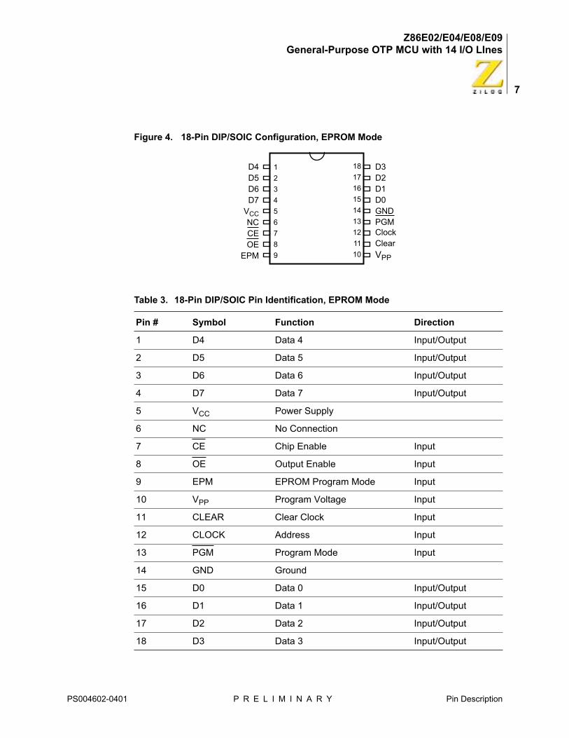
Figure 4. 18-Pin DIP/SOIC Configuration, EPROM Mode
Table 3. 18-Pin DIP/SOIC Pin Identification, EPROM Mode
Pin # Symbol Function Direction
1 D4 Data 4 Input/Output
2 D5 Data 5 Input/Output
3 D6 Data 6 Input/Output
4 D7 Data 7 Input/Output
5 VCC Power Supply
6 NC No Connection
7 CE Chip Enable Input
8 OE Output Enable Input
9 EPM EPROM Program Mode Input
10 VPP Program Voltage Input
11 CLEAR Clear Clock Input
12 CLOCK Address Input
13 PGM Program Mode Input
14 GND Ground
15 D0 Data 0 Input/Output
16 D1 Data 1 Input/Output
17 D2 Data 2 Input/Output
18 D3 Data 3 Input/Output
D4D5D6D7
VCCNCCEOE
EPM
D3D2D1D0GNDPGMClockClearVPP
18
17
16
15
14
13
12
11
10
1
2
3
4
5
6
7
8
9
PS004602-0401 P R E L I M I N A R Y Pin Description
Z86E02/E04/E08/E09General-Purpose OTP MCU with 14 I/O LInes
8
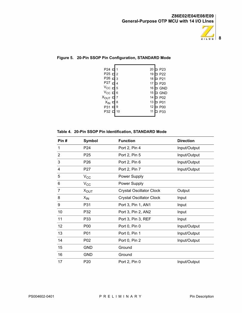
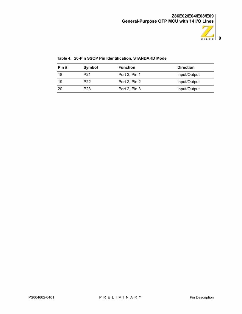
Figure 5. 20-Pin SSOP Pin Configuration, STANDARD Mode
Table 4. 20-Pin SSOP Pin Identification, STANDARD Mode
Pin # Symbol Function Direction
1 P24 Port 2, Pin 4 Input/Output
2 P25 Port 2, Pin 5 Input/Output
3 P26 Port 2, Pin 6 Input/Output
4 P27 Port 2, Pin 7 Input/Output
5 VCC Power Supply
6 VCC Power Supply
7 XOUT Crystal Oscillator Clock Output
8 XIN Crystal Oscillator Clock Input
9 P31 Port 3, Pin 1, AN1 Input
10 P32 Port 3, Pin 2, AN2 Input
11 P33 Port 3, Pin 3, REF Input
12 P00 Port 0, Pin 0 Input/Output
13 P01 Port 0, Pin 1 Input/Output
14 P02 Port 0, Pin 2 Input/Output
15 GND Ground
16 GND Ground
17 P20 Port 2, Pin 0 Input/Output
P24P25P26P27VCC
VCC
XOUT
XIN
P31P32
P23P22P21P20GNDGNDP02P01P00P33
20
19
18
17
16
15
14
13
12
11
1
2
3
4
5
6
7
8
9
10
PS004602-0401 P R E L I M I N A R Y Pin Description
Z86E02/E04/E08/E09General-Purpose OTP MCU with 14 I/O LInes
9
18 P21 Port 2, Pin 1 Input/Output
19 P22 Port 2, Pin 2 Input/Output
20 P23 Port 2, Pin 3 Input/Output
Table 4. 20-Pin SSOP Pin Identification, STANDARD Mode
Pin # Symbol Function Direction
PS004602-0401 P R E L I M I N A R Y Pin Description
Z86E02/E04/E08/E09General-Purpose OTP MCU with 14 I/O LInes
10
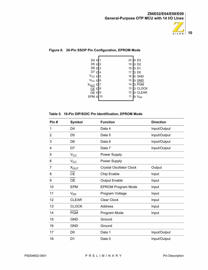
Figure 6. 20-Pin SSOP Pin Configuration, EPROM Mode
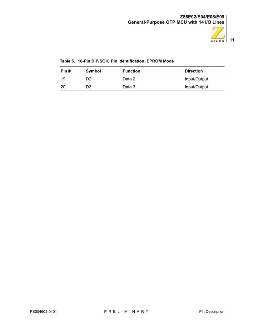
Table 5. 18-Pin DIP/SOIC Pin Identification, EPROM Mode
Pin # Symbol Function Direction
1 D4 Data 4 Input/Output
2 D5 Data 5 Input/Output
3 D6 Data 6 Input/Output
4 D7 Data 7 Input/Output
5 VCC Power Supply
6 VCC Power Supply
7 XOUT Crystal Oscillator Clock Output
8 CE Chip Enable Input
9 OE Output Enable Input
10 EPM EPROM Program Mode Input
11 VPP Program Voltage Input
12 CLEAR Clear Clock Input
13 CLOCK Address Input
14 PGM Program Mode Input
15 GND Ground
16 GND Ground
17 D0 Data 1 Input/Output
18 D1 Data 0 Input/Output
D4D5D6D7
VCC
VCC
XOUT
CEOE
EPM
D3D2D1D0GNDGNDPGMCLOCKCLEARVPP
20
19
18
17
16
15
14
13
12
11
1
2
3
4
5
6
7
8
9
10
PS004602-0401 P R E L I M I N A R Y Pin Description
Z86E02/E04/E08/E09General-Purpose OTP MCU with 14 I/O LInes
11
19 D2 Data 2 Input/Output
20 D3 Data 3 Input/Output
Table 5. 18-Pin DIP/SOIC Pin Identification, EPROM Mode
Pin # Symbol Function Direction
PS004602-0401 P R E L I M I N A R Y Pin Description
Z86E02/E04/E08/E09General-Purpose OTP MCU with 14 I/O LInes
12
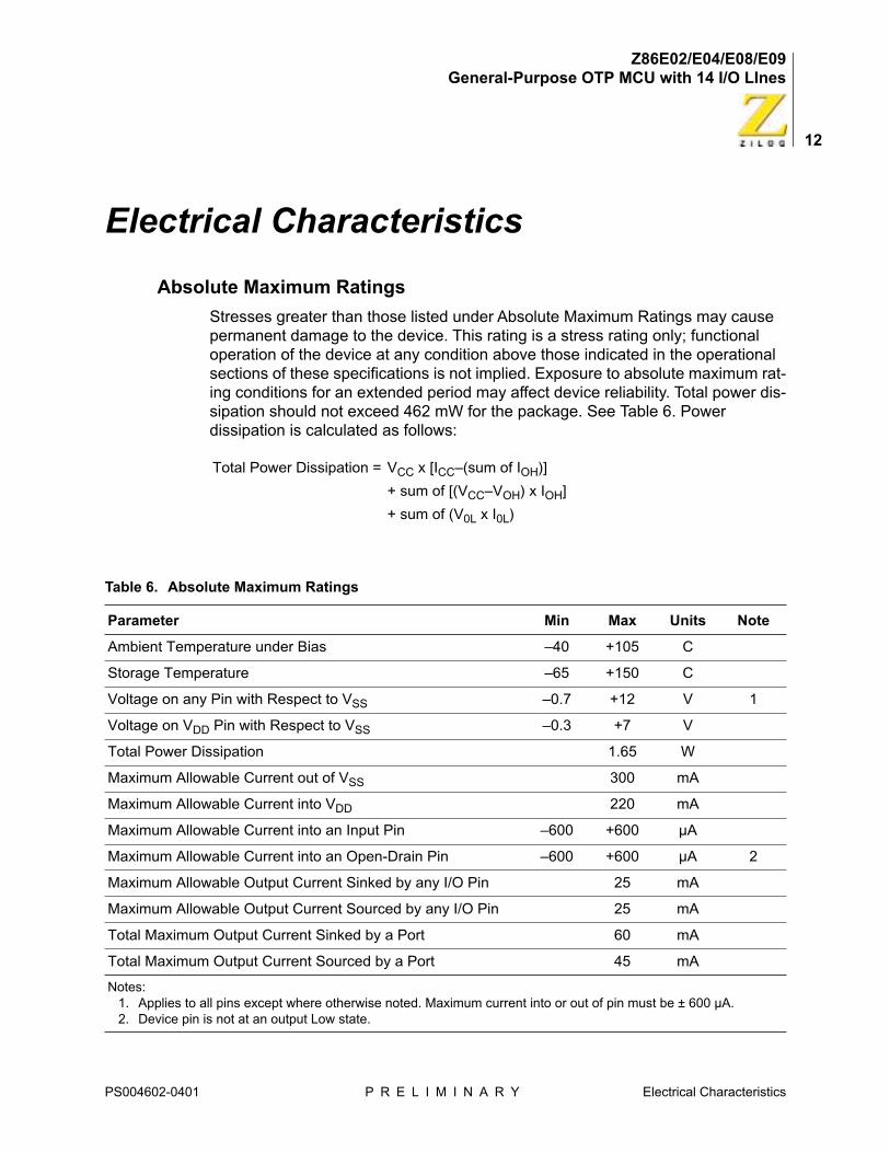
Electrical Characteristics
Absolute Maximum Ratings
Stresses greater than those listed under Absolute Maximum Ratings may cause permanent damage to the device. This rating is a stress rating only; functional operation of the device at any condition above those indicated in the operational sections of these specifications is not implied. Exposure to absolute maximum rat-ing conditions for an extended period may affect device reliability. Total power dis-sipation should not exceed 462 mW for the package. See Table 6. Power dissipation is calculated as follows:
Total Power Dissipation = VCC x [ICC–(sum of IOH)]
+ sum of [(VCC–VOH) x IOH]
+ sum of (V0L x I0L)
Table 6. Absolute Maximum Ratings
Parameter Min Max Units Note
Ambient Temperature under Bias –40 +105 C
Storage Temperature –65 +150 C
Voltage on any Pin with Respect to VSS –0.7 +12 V 1
Voltage on VDD Pin with Respect to VSS –0.3 +7 V
Total Power Dissipation 1.65 W
Maximum Allowable Current out of VSS 300 mA
Maximum Allowable Current into VDD 220 mA
Maximum Allowable Current into an Input Pin –600 +600 µA
Maximum Allowable Current into an Open-Drain Pin –600 +600 µA 2
Maximum Allowable Output Current Sinked by any I/O Pin 25 mA
Maximum Allowable Output Current Sourced by any I/O Pin 25 mA
Total Maximum Output Current Sinked by a Port 60 mA
Total Maximum Output Current Sourced by a Port 45 mA
Notes: 1. Applies to all pins except where otherwise noted. Maximum current into or out of pin must be ± 600 µA. 2. Device pin is not at an output Low state.
PS004602-0401 P R E L I M I N A R Y Electrical Characteristics
Z86E02/E04/E08/E09General-Purpose OTP MCU with 14 I/O LInes
13
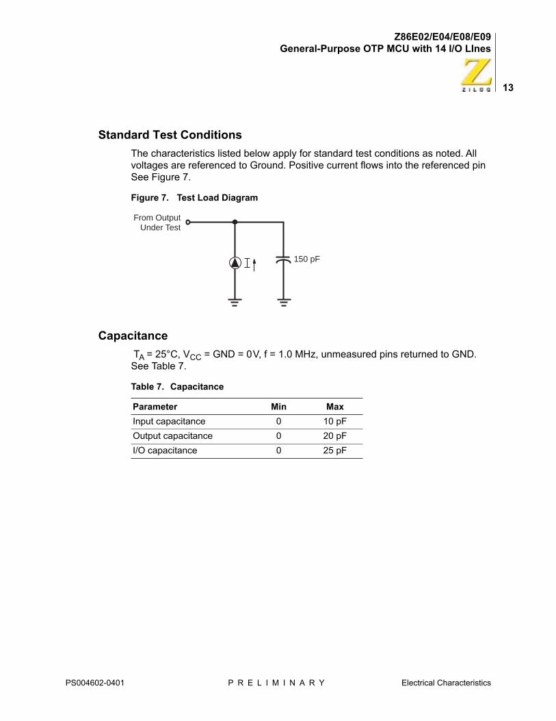
Standard Test Conditions
The characteristics listed below apply for standard test conditions as noted. All voltages are referenced to Ground. Positive current flows into the referenced pin See Figure 7.
Capacitance
TA = 25°C, VCC = GND = 0V, f = 1.0 MHz, unmeasured pins returned to GND. See Table 7.
Figure 7. Test Load Diagram
Table 7. Capacitance
Parameter Min Max
Input capacitance 0 10 pF
Output capacitance 0 20 pF
I/O capacitance 0 25 pF
From OutputUnder Test
150 pF
PS004602-0401 P R E L I M I N A R Y Electrical Characteristics
Z86E02/E04/E08/E09General-Purpose OTP MCU with 14 I/O LInes
14
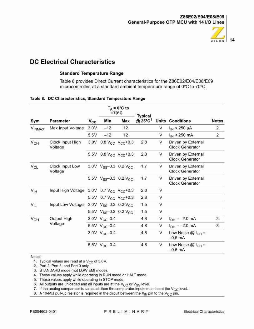
DC Electrical Characteristics
Standard Temperature Range
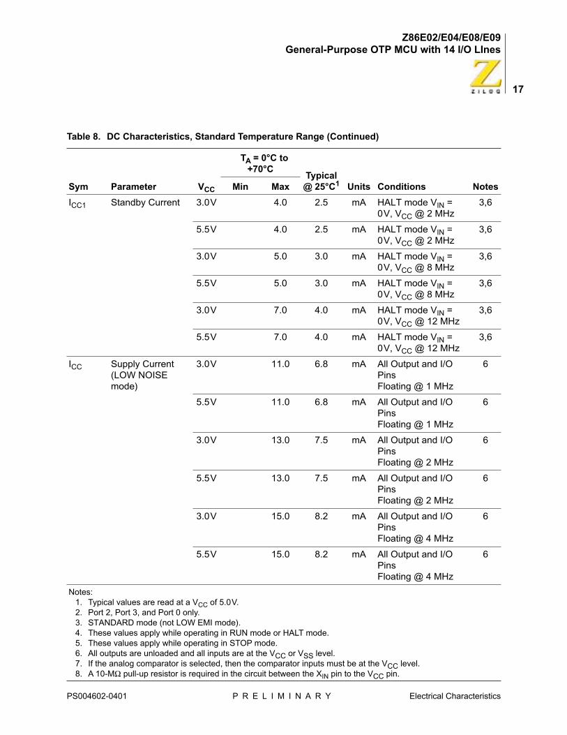
Table 8 provides Direct Current characteristics for the Z86E02/E04/E08/E09 microcontroller, at a standard ambient temperature range of 0ºC to 70ºC.
Table 8. DC Characteristics, Standard Temperature Range
Sym Parameter VCC
TA = 0°C to +70°C
Typical @ 25°C1 Units Conditions NotesMin Max
VINMAX Max Input Voltage 3.0V –12 12 V IIN < 250 µA 2
5.5V –12 12 V IIN < 250 mA 2
VCH Clock Input HighVoltage
3.0V 0.8 VCC VCC+0.3 2.8 V Driven by External Clock Generator
5.5V 0.8 VCC VCC+0.3 2.8 V Driven by External Clock Generator
VCL Clock Input Low Voltage
3.0V VSS–0.3 0.2 VCC 1.7 V Driven by External Clock Generator
5.5V VSS–0.3 0.2 VCC 1.7 V Driven by External Clock Generator
VIH Input High Voltage 3.0V 0.7 VCC VCC+0.3 2.8 V
5.5V 0.7 VCC VCC+0.3 2.8 V
VIL Input Low Voltage 3.0V VSS–0.3 0.2 VCC 1.5 V
5.5V VSS–0.3 0.2 VCC 1.5 V
VOH Output High Voltage
3.0V VCC–0.4 4.8 V IOH = –2.0 mA 3
5.5V VCC–0.4 4.8 V IOH = –2.0 mA 3
3.0V VCC–0.4 4.8 V Low Noise @ IOH = –0.5 mA
5.5V VCC–0.4 4.8 V Low Noise @ IOH = –0.5 mA
Notes: 1. Typical values are read at a VCC of 5.0V. 2. Port 2, Port 3, and Port 0 only.3. STANDARD mode (not LOW EMI mode).4. These values apply while operating in RUN mode or HALT mode.5. These values apply while operating in STOP mode.6. All outputs are unloaded and all inputs are at the VCC or VSS level.7. If the analog comparator is selected, then the comparator inputs must be at the VCC level.8. A 10-MΩ pull-up resistor is required in the circuit between the XIN pin to the VCC pin.
PS004602-0401 P R E L I M I N A R Y Electrical Characteristics
Z86E02/E04/E08/E09General-Purpose OTP MCU with 14 I/O LInes
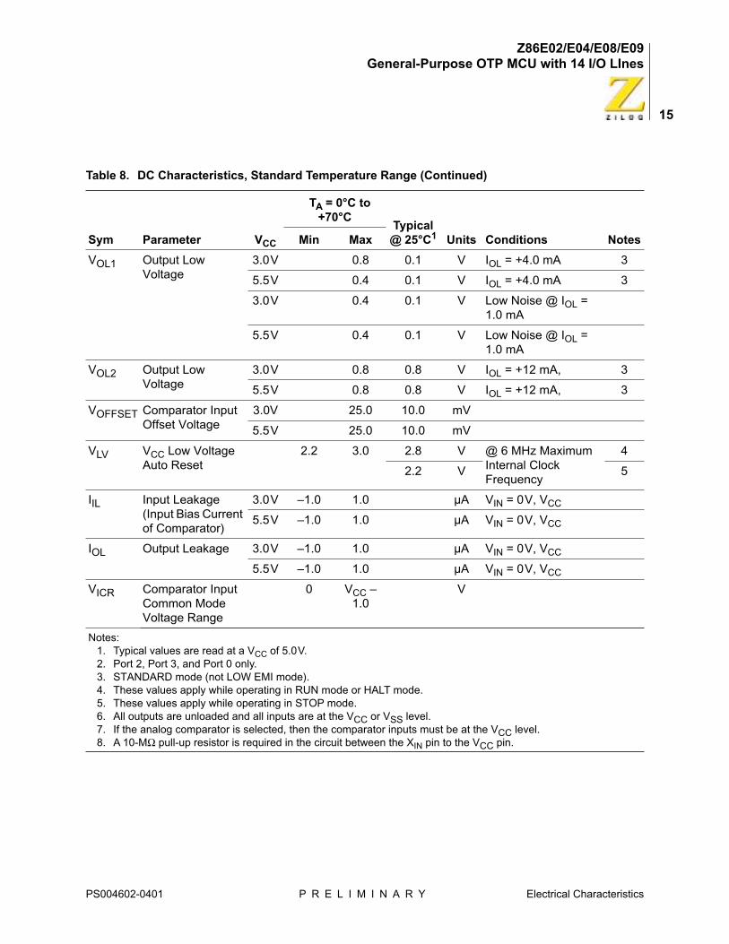
15
VOL1 Output Low Voltage
3.0V 0.8 0.1 V IOL = +4.0 mA 3
5.5V 0.4 0.1 V IOL = +4.0 mA 3
3.0V 0.4 0.1 V Low Noise @ IOL = 1.0 mA
5.5V 0.4 0.1 V Low Noise @ IOL = 1.0 mA
VOL2 Output Low Voltage
3.0V 0.8 0.8 V IOL = +12 mA, 3
5.5V 0.8 0.8 V IOL = +12 mA, 3
VOFFSET Comparator Input Offset Voltage
3.0V 25.0 10.0 mV
5.5V 25.0 10.0 mV
VLV VCC Low Voltage Auto Reset
2.2 3.0 2.8 V @ 6 MHz Maximum Internal Clock Frequency
4
2.2 V 5
IIL Input Leakage (Input Bias Current of Comparator)
3.0V –1.0 1.0 µA VIN = 0V, VCC
5.5V –1.0 1.0 µA VIN = 0V, VCC
IOL Output Leakage 3.0V –1.0 1.0 µA VIN = 0V, VCC
5.5V –1.0 1.0 µA VIN = 0V, VCC
VICR Comparator Input Common Mode Voltage Range
0 VCC –1.0
V
Table 8. DC Characteristics, Standard Temperature Range (Continued)
Sym Parameter VCC
TA = 0°C to +70°C
Typical @ 25°C1 Units Conditions NotesMin Max
Notes: 1. Typical values are read at a VCC of 5.0V. 2. Port 2, Port 3, and Port 0 only.3. STANDARD mode (not LOW EMI mode).4. These values apply while operating in RUN mode or HALT mode.5. These values apply while operating in STOP mode.6. All outputs are unloaded and all inputs are at the VCC or VSS level.7. If the analog comparator is selected, then the comparator inputs must be at the VCC level.8. A 10-MΩ pull-up resistor is required in the circuit between the XIN pin to the VCC pin.
PS004602-0401 P R E L I M I N A R Y Electrical Characteristics
Z86E02/E04/E08/E09General-Purpose OTP MCU with 14 I/O LInes
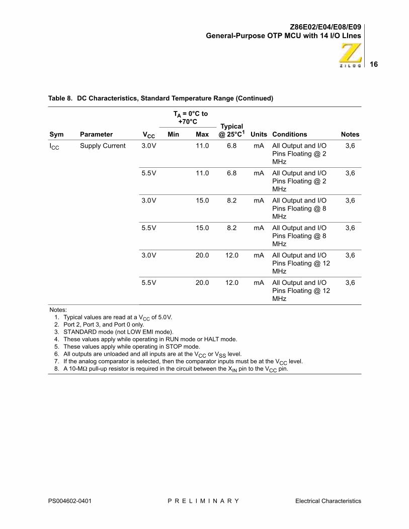
16
ICC Supply Current 3.0V 11.0 6.8 mA All Output and I/O Pins Floating @ 2 MHz
3,6
5.5V 11.0 6.8 mA All Output and I/O Pins Floating @ 2 MHz
3,6
3.0V 15.0 8.2 mA All Output and I/O Pins Floating @ 8 MHz
3,6
5.5V 15.0 8.2 mA All Output and I/O Pins Floating @ 8 MHz
3,6
3.0V 20.0 12.0 mA All Output and I/O Pins Floating @ 12 MHz
3,6
5.5V 20.0 12.0 mA All Output and I/O Pins Floating @ 12 MHz
3,6
Table 8. DC Characteristics, Standard Temperature Range (Continued)
Sym Parameter VCC
TA = 0°C to +70°C
Typical @ 25°C1 Units Conditions NotesMin Max
Notes: 1. Typical values are read at a VCC of 5.0V. 2. Port 2, Port 3, and Port 0 only.3. STANDARD mode (not LOW EMI mode).4. These values apply while operating in RUN mode or HALT mode.5. These values apply while operating in STOP mode.6. All outputs are unloaded and all inputs are at the VCC or VSS level.7. If the analog comparator is selected, then the comparator inputs must be at the VCC level.8. A 10-MΩ pull-up resistor is required in the circuit between the XIN pin to the VCC pin.
PS004602-0401 P R E L I M I N A R Y Electrical Characteristics
Z86E02/E04/E08/E09General-Purpose OTP MCU with 14 I/O LInes
17
ICC1 Standby Current 3.0V 4.0 2.5 mA HALT mode VIN = 0V, VCC @ 2 MHz
3,6
5.5V 4.0 2.5 mA HALT mode VIN = 0V, VCC @ 2 MHz
3,6
3.0V 5.0 3.0 mA HALT mode VIN = 0V, VCC @ 8 MHz
3,6
5.5V 5.0 3.0 mA HALT mode VIN = 0V, VCC @ 8 MHz
3,6
3.0V 7.0 4.0 mA HALT mode VIN = 0V, VCC @ 12 MHz
3,6
5.5V 7.0 4.0 mA HALT mode VIN = 0V, VCC @ 12 MHz
3,6
ICC Supply Current (LOW NOISE mode)
3.0V 11.0 6.8 mA All Output and I/O PinsFloating @ 1 MHz
6
5.5V 11.0 6.8 mA All Output and I/O PinsFloating @ 1 MHz
6
3.0V 13.0 7.5 mA All Output and I/O PinsFloating @ 2 MHz
6
5.5V 13.0 7.5 mA All Output and I/O PinsFloating @ 2 MHz
6
3.0V 15.0 8.2 mA All Output and I/O PinsFloating @ 4 MHz
6
5.5V 15.0 8.2 mA All Output and I/O PinsFloating @ 4 MHz
6
Table 8. DC Characteristics, Standard Temperature Range (Continued)
Sym Parameter VCC
TA = 0°C to +70°C
Typical @ 25°C1 Units Conditions NotesMin Max
Notes: 1. Typical values are read at a VCC of 5.0V. 2. Port 2, Port 3, and Port 0 only.3. STANDARD mode (not LOW EMI mode).4. These values apply while operating in RUN mode or HALT mode.5. These values apply while operating in STOP mode.6. All outputs are unloaded and all inputs are at the VCC or VSS level.7. If the analog comparator is selected, then the comparator inputs must be at the VCC level.8. A 10-MΩ pull-up resistor is required in the circuit between the X pin to the V pin.
PS004602-0401 P R E L I M I N A R Y Electrical Characteristics
IN CC

Z86E02/E04/E08/E09General-Purpose OTP MCU with 14 I/O LInes
18
ICC1 Standby Current (LOW NOISE mode)
3.0V 4.0 2.5 mA HALT mode VIN = 0V,VCC @ 1 MHz
6
5.5V 4.0 2.5 mA HALT mode VIN = 0V,VCC @ 1 MHz
6
3.0V 3.0 2.8 mA HALT mode VIN = 0V,VCC @ 2 MHz
6
5.5V 3.0 2.8 mA HALT mode VIN = 0V,VCC @ 2 MHz
6
3.0V 5.0 3.0 mA HALT mode VIN = 0V,VCC @ 4 MHz
6
5.5V 5.0 3.0 mA HALT mode VIN = 0V,VCC @ 4 MHz
6
ICC2 Standby Current 3.0V 10.0 1.0 µA STOP mode VIN = 0V, VCC; WDT is not Running
6,7,8
5.5V 10.0 1.0 µA STOP mode VIN = 0V,VCC; WDT is not Running
6,7,8
IALL Auto Latch Low Current
3.0V 32.0 16 µA 0V < VIN < VCC
5.5V 32.0 16 µA 0V < VIN < VCC
IALH Auto Latch High Current
3.0V –16.0 –8.0 0V < VIN < VCCµA
5.5V –16.0 –8.0 µA 0V < VIN < VCC
Table 8. DC Characteristics, Standard Temperature Range (Continued)
Sym Parameter VCC
TA = 0°C to +70°C
Typical @ 25°C1 Units Conditions NotesMin Max
Notes: 1. Typical values are read at a VCC of 5.0V. 2. Port 2, Port 3, and Port 0 only.3. STANDARD mode (not LOW EMI mode).4. These values apply while operating in RUN mode or HALT mode.5. These values apply while operating in STOP mode.6. All outputs are unloaded and all inputs are at the VCC or VSS level.7. If the analog comparator is selected, then the comparator inputs must be at the VCC level.8. A 10-MΩ pull-up resistor is required in the circuit between the XIN pin to the VCC pin.
PS004602-0401 P R E L I M I N A R Y Electrical Characteristics
Z86E02/E04/E08/E09General-Purpose OTP MCU with 14 I/O LInes
19
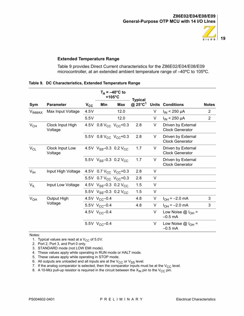
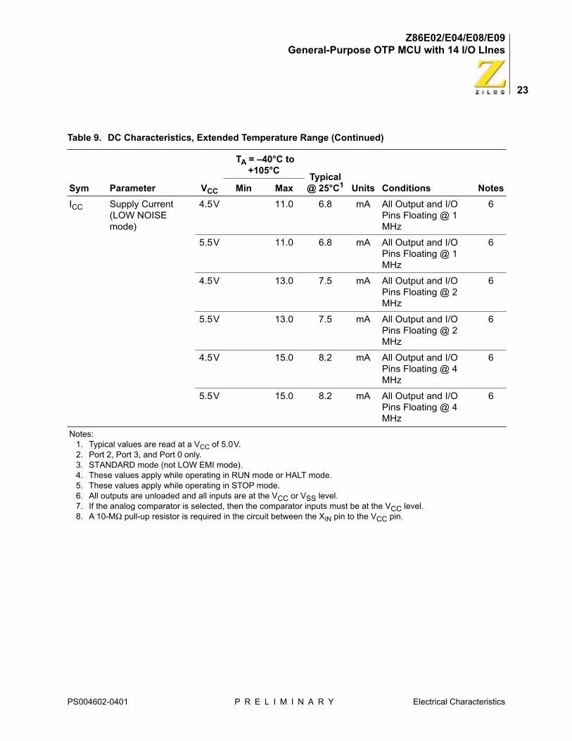
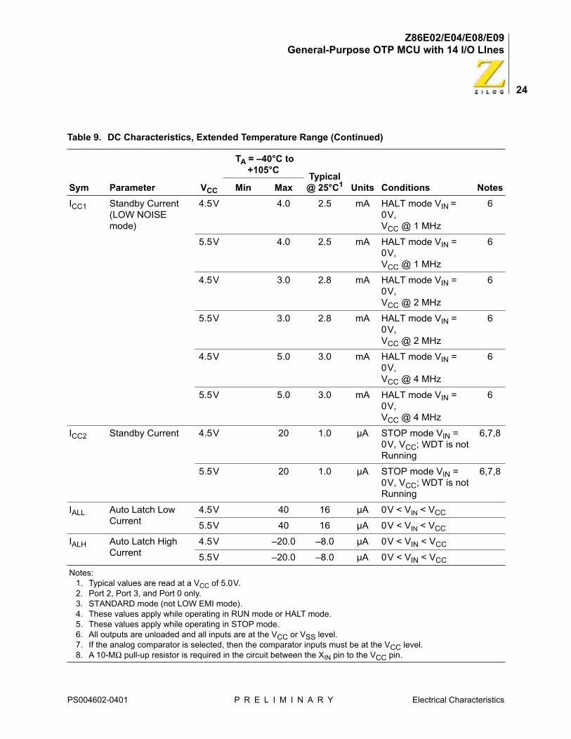
Extended Temperature Range
Table 9 provides Direct Current characteristics for the Z86E02/E04/E08/E09 microcontroller, at an extended ambient temperature range of –40ºC to 105ºC.
Table 9. DC Characteristics, Extended Temperature Range
Sym Parameter VCC
TA = –40°C to +105°C
Typical @ 25°C1 Units Conditions NotesMin Max
VINMAX Max Input Voltage 4.5V 12.0 V IIN < 250 µA 2
5.5V 12.0 V IIN < 250 µA 2
VCH Clock Input HighVoltage
4.5V 0.8 VCC VCC+0.3 2.8 V Driven by External Clock Generator
5.5V 0.8 VCC VCC+0.3 2.8 V Driven by External Clock Generator
VCL Clock Input Low Voltage
4.5V VSS–0.3 0.2 VCC 1.7 V Driven by External Clock Generator
5.5V VSS–0.3 0.2 VCC 1.7 V Driven by External Clock Generator
VIH Input High Voltage 4.5V 0.7 VCC VCC+0.3 2.8 V
5.5V 0.7 VCC VCC+0.3 2.8 V
VIL Input Low Voltage 4.5V VSS–0.3 0.2 VCC 1.5 V
5.5V VSS–0.3 0.2 VCC 1.5 V
VOH Output High Voltage
4.5V VCC–0.4 4.8 V IOH = –2.0 mA 3
5.5V VCC–0.4 4.8 V IOH = –2.0 mA 3
4.5V VCC–0.4 V Low Noise @ IOH = –0.5 mA
5.5V VCC–0.4 V Low Noise @ IOH = –0.5 mA
Notes: 1. Typical values are read at a VCC of 5.0V. 2. Port 2, Port 3, and Port 0 only.3. STANDARD mode (not LOW EMI mode).4. These values apply while operating in RUN mode or HALT mode.5. These values apply while operating in STOP mode.6. All outputs are unloaded and all inputs are at the VCC or VSS level.7. If the analog comparator is selected, then the comparator inputs must be at the VCC level.8. A 10-MΩ pull-up resistor is required in the circuit between the XIN pin to the VCC pin.
PS004602-0401 P R E L I M I N A R Y Electrical Characteristics
Z86E02/E04/E08/E09General-Purpose OTP MCU with 14 I/O LInes
20
VOL1 Output Low Voltage
4.5V 0.4 0.1 V IOL = +4.0 mA 3
5.5V 0.4 0.1 V IOL = +4.0 mA 3
4.5V 0.4 0.1 V Low Noise @ IOL = 1.0 mA
5.5V 0.4 0.1 V Low Noise @ IOL = 1.0 mA
VOL2 Output Low Voltage 4.5V 1.0 0.3 V IOL = +12 mA 3
5.5V 1.0 0.3 V IOL = +12 mA 3
VOFFSET Comparator Input Offset Voltage
4.5V 25.0 10.0 mV
5.5V 25.0 10.0 mV
VLV VCC Low Voltage Auto Reset
1.8 3.8 2.8 V @ 6 MHz Maximum Internal Clock Frequency
4
2.2 V 5
IIL Input Leakage (Input Bias Current of Comparator)
4.5V –1.0 1.0 µA VIN = 0V, VCC
5.5V –1.0 1.0 µA VIN = 0V, VCC
IOL Output Leakage 4.5V –1.0 1.0 µA VIN = 0V, VCC
5.5V –1.0 1.0 µA VIN = 0V, VCC
VICR Comparator Input Common Mode Voltage Range
0 VCC –1.5
V
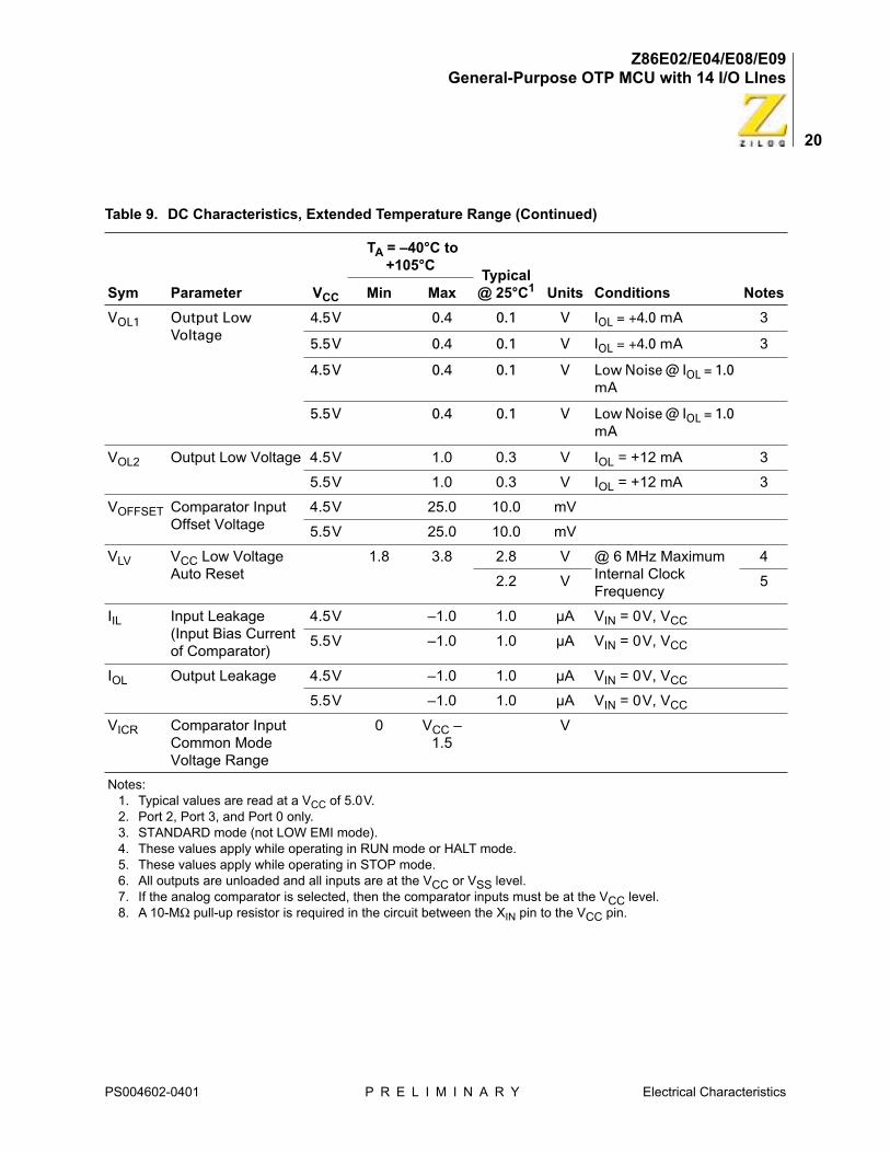
Table 9. DC Characteristics, Extended Temperature Range (Continued)
Sym Parameter VCC
TA = –40°C to +105°C
Typical @ 25°C1 Units Conditions NotesMin Max
Notes: 1. Typical values are read at a VCC of 5.0V. 2. Port 2, Port 3, and Port 0 only.3. STANDARD mode (not LOW EMI mode).4. These values apply while operating in RUN mode or HALT mode.5. These values apply while operating in STOP mode.6. All outputs are unloaded and all inputs are at the VCC or VSS level.7. If the analog comparator is selected, then the comparator inputs must be at the VCC level.8. A 10-MΩ pull-up resistor is required in the circuit between the XIN pin to the VCC pin.
PS004602-0401 P R E L I M I N A R Y Electrical Characteristics

Z86E02/E04/E08/E09General-Purpose OTP MCU with 14 I/O LInes
21
ICC Supply Current 4.5V 11.0 6.8 mA All Output and I/O Pins Floating @ 2 MHz
3,6
5.5V 11.0 6.8 mA All Output and I/O Pins Floating @ 2 MHz
3,6
4.5V 15.0 8.2 mA All Output and I/O Pins Floating @ 8 MHz
3,6
5.5V 15.0 8.2 mA All Output and I/O Pins Floating @ 8 MHz
3,6
4.5V 20.0 12.0 mA All Output and I/O Pins Floating @ 12 MHz
3,6
5.5V 20.0 12.0 mA All Output and I/O Pins Floating @ 12 MHz
3,6
Table 9. DC Characteristics, Extended Temperature Range (Continued)
Sym Parameter VCC
TA = –40°C to +105°C
Typical @ 25°C1 Units Conditions NotesMin Max
Notes: 1. Typical values are read at a VCC of 5.0V. 2. Port 2, Port 3, and Port 0 only.3. STANDARD mode (not LOW EMI mode).4. These values apply while operating in RUN mode or HALT mode.5. These values apply while operating in STOP mode.6. All outputs are unloaded and all inputs are at the VCC or VSS level.7. If the analog comparator is selected, then the comparator inputs must be at the VCC level.8. A 10-MΩ pull-up resistor is required in the circuit between the XIN pin to the VCC pin.
PS004602-0401 P R E L I M I N A R Y Electrical Characteristics
Z86E02/E04/E08/E09General-Purpose OTP MCU with 14 I/O LInes
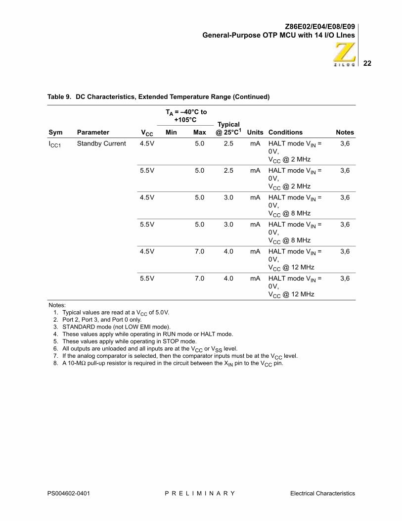
22
ICC1 Standby Current 4.5V 5.0 2.5 mA HALT mode VIN = 0V, VCC @ 2 MHz
3,6
5.5V 5.0 2.5 mA HALT mode VIN = 0V, VCC @ 2 MHz
3,6
4.5V 5.0 3.0 mA HALT mode VIN = 0V, VCC @ 8 MHz
3,6
5.5V 5.0 3.0 mA HALT mode VIN = 0V, VCC @ 8 MHz
3,6
4.5V 7.0 4.0 mA HALT mode VIN = 0V, VCC @ 12 MHz
3,6
5.5V 7.0 4.0 mA HALT mode VIN = 0V, VCC @ 12 MHz
3,6
Table 9. DC Characteristics, Extended Temperature Range (Continued)
Sym Parameter VCC
TA = –40°C to +105°C
Typical @ 25°C1 Units Conditions NotesMin Max
Notes: 1. Typical values are read at a VCC of 5.0V. 2. Port 2, Port 3, and Port 0 only.3. STANDARD mode (not LOW EMI mode).4. These values apply while operating in RUN mode or HALT mode.5. These values apply while operating in STOP mode.6. All outputs are unloaded and all inputs are at the VCC or VSS level.7. If the analog comparator is selected, then the comparator inputs must be at the VCC level.8. A 10-MΩ pull-up resistor is required in the circuit between the XIN pin to the VCC pin.
PS004602-0401 P R E L I M I N A R Y Electrical Characteristics
Z86E02/E04/E08/E09General-Purpose OTP MCU with 14 I/O LInes
23
ICC Supply Current (LOW NOISE mode)
4.5V 11.0 6.8 mA All Output and I/O Pins Floating @ 1 MHz
6
5.5V 11.0 6.8 mA All Output and I/O Pins Floating @ 1 MHz
6
4.5V 13.0 7.5 mA All Output and I/O Pins Floating @ 2 MHz
6
5.5V 13.0 7.5 mA All Output and I/O Pins Floating @ 2 MHz
6
4.5V 15.0 8.2 mA All Output and I/O Pins Floating @ 4 MHz
6
5.5V 15.0 8.2 mA All Output and I/O Pins Floating @ 4 MHz
6
Table 9. DC Characteristics, Extended Temperature Range (Continued)
Sym Parameter VCC
TA = –40°C to +105°C
Typical @ 25°C1 Units Conditions NotesMin Max
Notes: 1. Typical values are read at a VCC of 5.0V. 2. Port 2, Port 3, and Port 0 only.3. STANDARD mode (not LOW EMI mode).4. These values apply while operating in RUN mode or HALT mode.5. These values apply while operating in STOP mode.6. All outputs are unloaded and all inputs are at the VCC or VSS level.7. If the analog comparator is selected, then the comparator inputs must be at the VCC level.8. A 10-MΩ pull-up resistor is required in the circuit between the XIN pin to the VCC pin.
PS004602-0401 P R E L I M I N A R Y Electrical Characteristics
Z86E02/E04/E08/E09General-Purpose OTP MCU with 14 I/O LInes
24
ICC1 Standby Current (LOW NOISE mode)
4.5V 4.0 2.5 mA HALT mode VIN = 0V, VCC @ 1 MHz
6
5.5V 4.0 2.5 mA HALT mode VIN = 0V, VCC @ 1 MHz
6
4.5V 3.0 2.8 mA HALT mode VIN = 0V, VCC @ 2 MHz
6
5.5V 3.0 2.8 mA HALT mode VIN = 0V, VCC @ 2 MHz
6
4.5V 5.0 3.0 mA HALT mode VIN = 0V, VCC @ 4 MHz
6
5.5V 5.0 3.0 mA HALT mode VIN = 0V, VCC @ 4 MHz
6
ICC2 Standby Current 4.5V 20 1.0 µA STOP mode VIN = 0V, VCC; WDT is not Running
6,7,8
5.5V 20 1.0 µA STOP mode VIN = 0V, VCC; WDT is not Running
6,7,8
IALL Auto Latch LowCurrent
4.5V 40 16 µA 0V < VIN < VCC
5.5V 40 16 µA 0V < VIN < VCC
IALH Auto Latch High Current
4.5V –20.0 –8.0 µA 0V < VIN < VCC
5.5V –20.0 –8.0 µA 0V < VIN < VCC
Table 9. DC Characteristics, Extended Temperature Range (Continued)
Sym Parameter VCC
TA = –40°C to +105°C
Typical @ 25°C1 Units Conditions NotesMin Max
Notes: 1. Typical values are read at a VCC of 5.0V. 2. Port 2, Port 3, and Port 0 only.3. STANDARD mode (not LOW EMI mode).4. These values apply while operating in RUN mode or HALT mode.5. These values apply while operating in STOP mode.6. All outputs are unloaded and all inputs are at the VCC or VSS level.7. If the analog comparator is selected, then the comparator inputs must be at the VCC level.8. A 10-MΩ pull-up resistor is required in the circuit between the XIN pin to the VCC pin.
PS004602-0401 P R E L I M I N A R Y Electrical Characteristics
Z86E02/E04/E08/E09General-Purpose OTP MCU with 14 I/O LInes
25
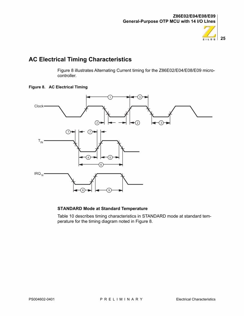
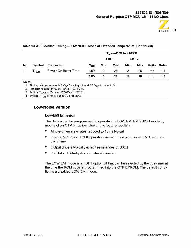
AC Electrical Timing Characteristics
Figure 8 illustrates Alternating Current timing for the Z86E02/E04/E08/E09 micro-controller.
STANDARD Mode at Standard Temperature
Table 10 describes timing characteristics in STANDARD mode at standard tem-perature for the timing diagram noted in Figure 8.
Figure 8. AC Electrical Timing
Clock
1 3
4
8
2 2 3
6
5
7 7
9
IRQ N
TIN
PS004602-0401 P R E L I M I N A R Y Electrical Characteristics
Z86E02/E04/E08/E09General-Purpose OTP MCU with 14 I/O LInes
26
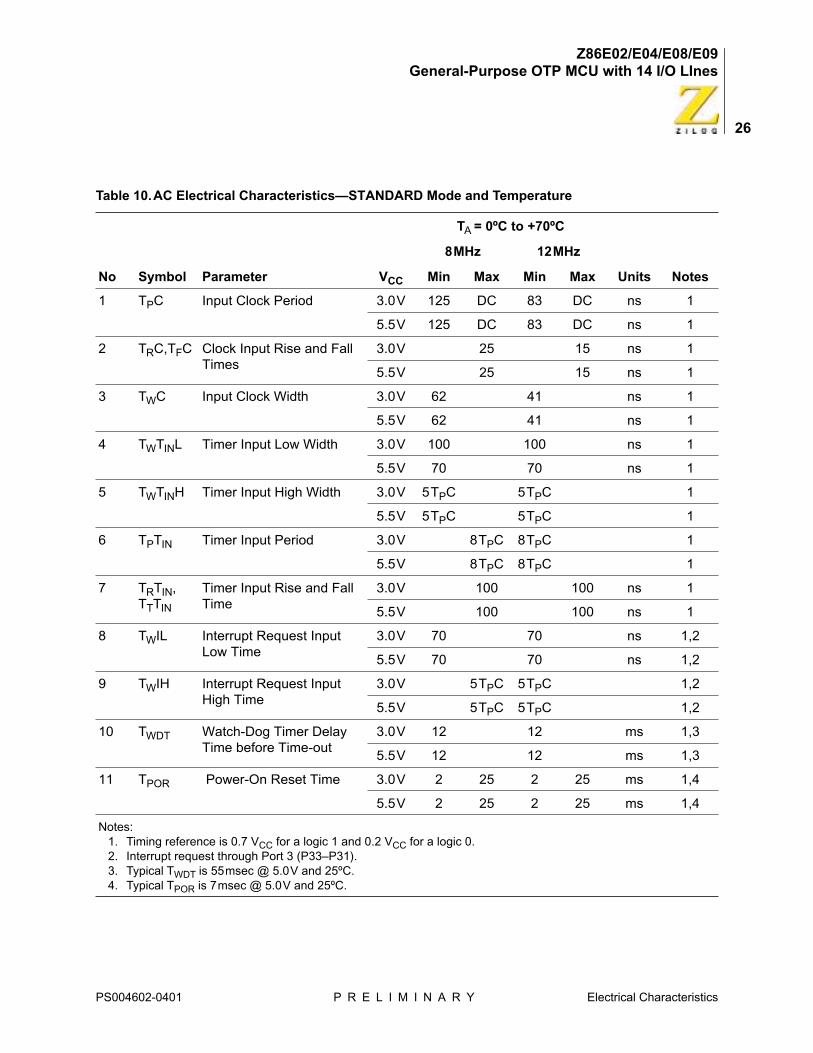
Table 10.AC Electrical Characteristics—STANDARD Mode and Temperature
No Symbol Parameter VCC
TA = 0ºC to +70ºC
Units Notes
8MHz 12MHz
Min Max Min Max
1 TPC Input Clock Period 3.0V 125 DC 83 DC ns 1
5.5V 125 DC 83 DC ns 1
2 TRC,TFC Clock Input Rise and Fall Times
3.0V 25 15 ns 1
5.5V 25 15 ns 1
3 TWC Input Clock Width 3.0V 62 41 ns 1
5.5V 62 41 ns 1
4 TWTINL Timer Input Low Width 3.0V 100 100 ns 1
5.5V 70 70 ns 1
5 TWTINH Timer Input High Width 3.0V 5TPC 5TPC 1
5.5V 5TPC 5TPC 1
6 TPTIN Timer Input Period 3.0V 8TPC 8TPC 1
5.5V 8TPC 8TPC 1
7 TRTIN, TTTIN
Timer Input Rise and Fall Time
3.0V 100 100 ns 1
5.5V 100 100 ns 1
8 TWIL Interrupt Request Input Low Time
3.0V 70 70 ns 1,2
5.5V 70 70 ns 1,2
9 TWIH Interrupt Request Input High Time
3.0V 5TPC 5TPC 1,2
5.5V 5TPC 5TPC 1,2
10 TWDT Watch-Dog Timer Delay Time before Time-out
3.0V 12 12 ms 1,3
5.5V 12 12 ms 1,3
11 TPOR Power-On Reset Time 3.0V 2 25 2 25 ms 1,4
5.5V 2 25 2 25 ms 1,4
Notes: 1. Timing reference is 0.7 VCC for a logic 1 and 0.2 VCC for a logic 0.2. Interrupt request through Port 3 (P33–P31).3. Typical TWDT is 55msec @ 5.0V and 25ºC.4. Typical TPOR is 7msec @ 5.0V and 25ºC.
PS004602-0401 P R E L I M I N A R Y Electrical Characteristics
Z86E02/E04/E08/E09General-Purpose OTP MCU with 14 I/O LInes
27
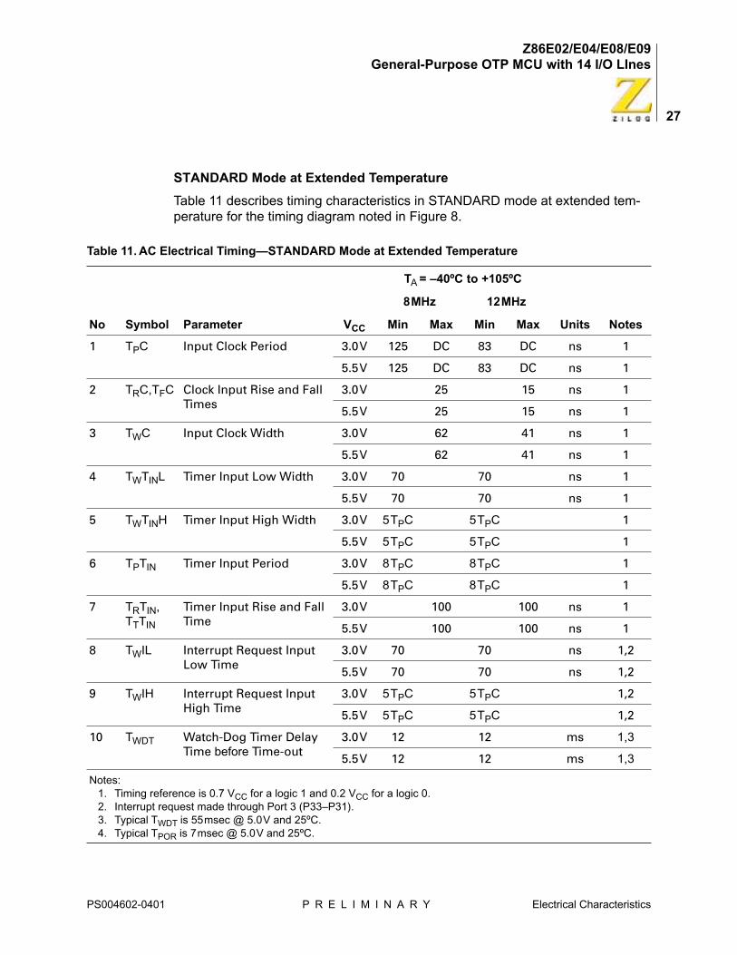
STANDARD Mode at Extended Temperature
Table 11 describes timing characteristics in STANDARD mode at extended tem-perature for the timing diagram noted in Figure 8.
Table 11. AC Electrical Timing—STANDARD Mode at Extended Temperature
No Symbol Parameter VCC
TA = –40ºC to +105ºC
Units Notes
8MHz 12MHz
Min Max Min Max
1 TPC Input Clock Period 3.0V 125 DC 83 DC ns 1
5.5V 125 DC 83 DC ns 1
2 TRC,TFC Clock Input Rise and Fall Times
3.0V 25 15 ns 1
5.5V 25 15 ns 1
3 TWC Input Clock Width 3.0V 62 41 ns 1
5.5V 62 41 ns 1
4 TWTINL Timer Input Low Width 3.0V 70 70 ns 1
5.5V 70 70 ns 1
5 TWTINH Timer Input High Width 3.0V 5TPC 5TPC 1
5.5V 5TPC 5TPC 1
6 TPTIN Timer Input Period 3.0V 8TPC 8TPC 1
5.5V 8TPC 8TPC 1
7 TRTIN, TTTIN
Timer Input Rise and Fall Time
3.0V 100 100 ns 1
5.5V 100 100 ns 1
8 TWIL Interrupt Request Input Low Time
3.0V 70 70 ns 1,2
5.5V 70 70 ns 1,2
9 TWIH Interrupt Request Input High Time
3.0V 5TPC 5TPC 1,2
5.5V 5TPC 5TPC 1,2
10 TWDT Watch-Dog Timer Delay Time before Time-out
3.0V 12 12 ms 1,3
5.5V 12 12 ms 1,3
Notes: 1. Timing reference is 0.7 VCC for a logic 1 and 0.2 VCC for a logic 0.2. Interrupt request made through Port 3 (P33–P31).3. Typical TWDT is 55msec @ 5.0V and 25ºC.4. Typical TPOR is 7msec @ 5.0V and 25ºC.
PS004602-0401 P R E L I M I N A R Y Electrical Characteristics
Z86E02/E04/E08/E09General-Purpose OTP MCU with 14 I/O LInes
28
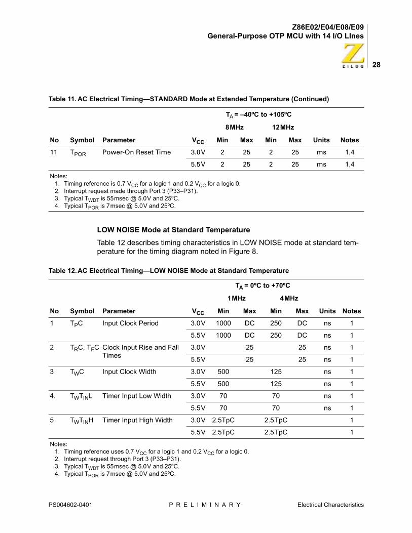
LOW NOISE Mode at Standard Temperature
Table 12 describes timing characteristics in LOW NOISE mode at standard tem-perature for the timing diagram noted in Figure 8.
11 TPOR Power-On Reset Time 3.0V 2 25 2 25 ms 1,4
5.5V 2 25 2 25 ms 1,4
Table 12.AC Electrical Timing—LOW NOISE Mode at Standard Temperature
No Symbol Parameter VCC
TA = 0ºC to +70ºC
Units Notes
1MHz 4MHz
Min Max Min Max
1 TPC Input Clock Period 3.0V 1000 DC 250 DC ns 1
5.5V 1000 DC 250 DC ns 1
2 TRC, TFC Clock Input Rise and Fall Times
3.0V 25 25 ns 1
5.5V 25 25 ns 1
3 TWC Input Clock Width 3.0V 500 125 ns 1
5.5V 500 125 ns 1
4. TWTINL Timer Input Low Width 3.0V 70 70 ns 1
5.5V 70 70 ns 1
5 TWTINH Timer Input High Width 3.0V 2.5TpC 2.5TpC 1
5.5V 2.5TpC 2.5TpC 1
Notes: 1. Timing reference uses 0.7 VCC for a logic 1 and 0.2 VCC for a logic 0.2. Interrupt request through Port 3 (P33–P31).3. Typical TWDT is 55msec @ 5.0V and 25ºC.4. Typical TPOR is 7msec @ 5.0V and 25ºC.
Table 11. AC Electrical Timing—STANDARD Mode at Extended Temperature (Continued)
No Symbol Parameter VCC
TA = –40ºC to +105ºC
Units Notes
8MHz 12MHz
Min Max Min Max
Notes: 1. Timing reference is 0.7 VCC for a logic 1 and 0.2 VCC for a logic 0.2. Interrupt request made through Port 3 (P33–P31).3. Typical TWDT is 55msec @ 5.0V and 25ºC.4. Typical TPOR is 7msec @ 5.0V and 25ºC.
PS004602-0401 P R E L I M I N A R Y Electrical Characteristics
Z86E02/E04/E08/E09General-Purpose OTP MCU with 14 I/O LInes
29
6 TPTIN Timer Input Period 3.0V 4TpC 4TpC 1
5.5V 4TpC 4TpC 1
7 TRTIN, TTTIN
Timer Input Rise and Fall Time
3.0V 100 100 ns 1
5.5V 100 100 ns 1
8 TWIL Low Time
Interrupt Request Input 3.0V 70 70 ns 1,2
5.5V 70 70 ns 1,2
9 TWIH High Time
Interrupt Request Input 3.0V 2.5TpC 2.5TpC 1,2
5.5V 2.5TpC 2.5TpC 1,2
10 TWDT Watch-Dog Timer Delay Time for Time-out
3.0V 12 12 ms 1,3
5.5V 12 12 ms 1,3
11 TPOR Power-On Reset Time 3.0V 2 25 2 25 ms 1,4
5.5V 2 25 2 25 ms 1,4
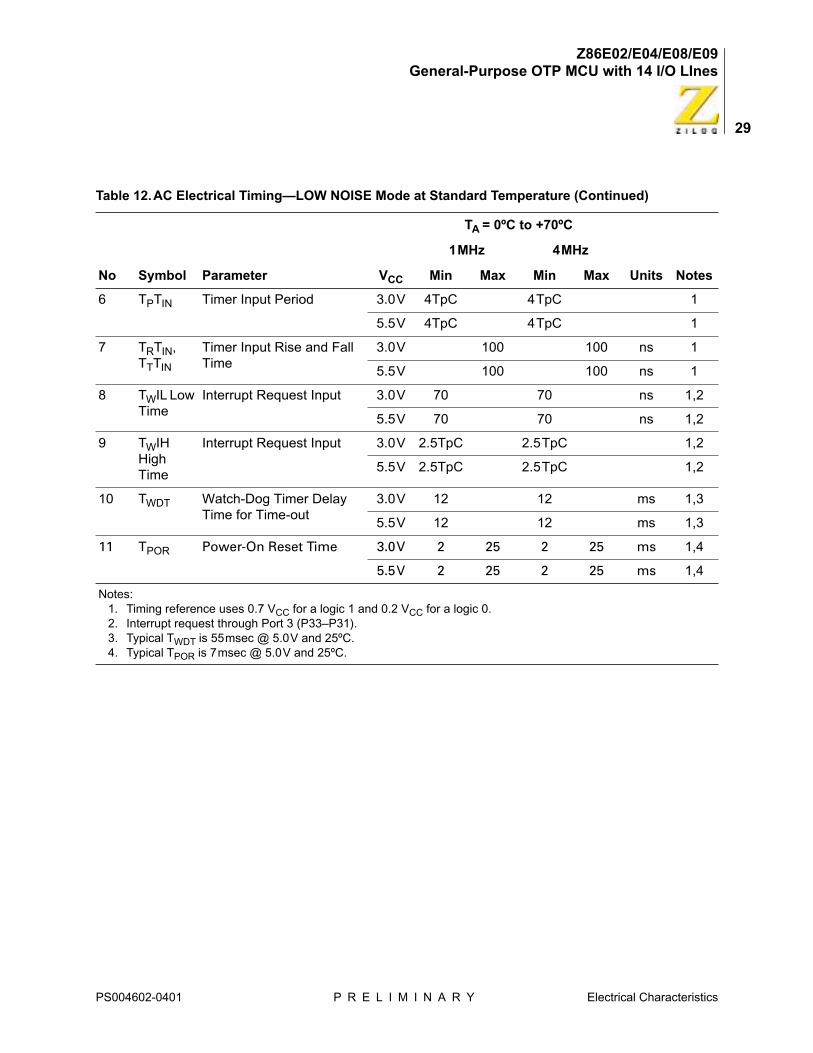
Table 12.AC Electrical Timing—LOW NOISE Mode at Standard Temperature (Continued)
No Symbol Parameter VCC
TA = 0ºC to +70ºC
Units Notes
1MHz 4MHz
Min Max Min Max
Notes: 1. Timing reference uses 0.7 VCC for a logic 1 and 0.2 VCC for a logic 0.2. Interrupt request through Port 3 (P33–P31).3. Typical TWDT is 55msec @ 5.0V and 25ºC.4. Typical TPOR is 7msec @ 5.0V and 25ºC.
PS004602-0401 P R E L I M I N A R Y Electrical Characteristics
Z86E02/E04/E08/E09General-Purpose OTP MCU with 14 I/O LInes
30
LOW NOISE Mode at Extended Temperature
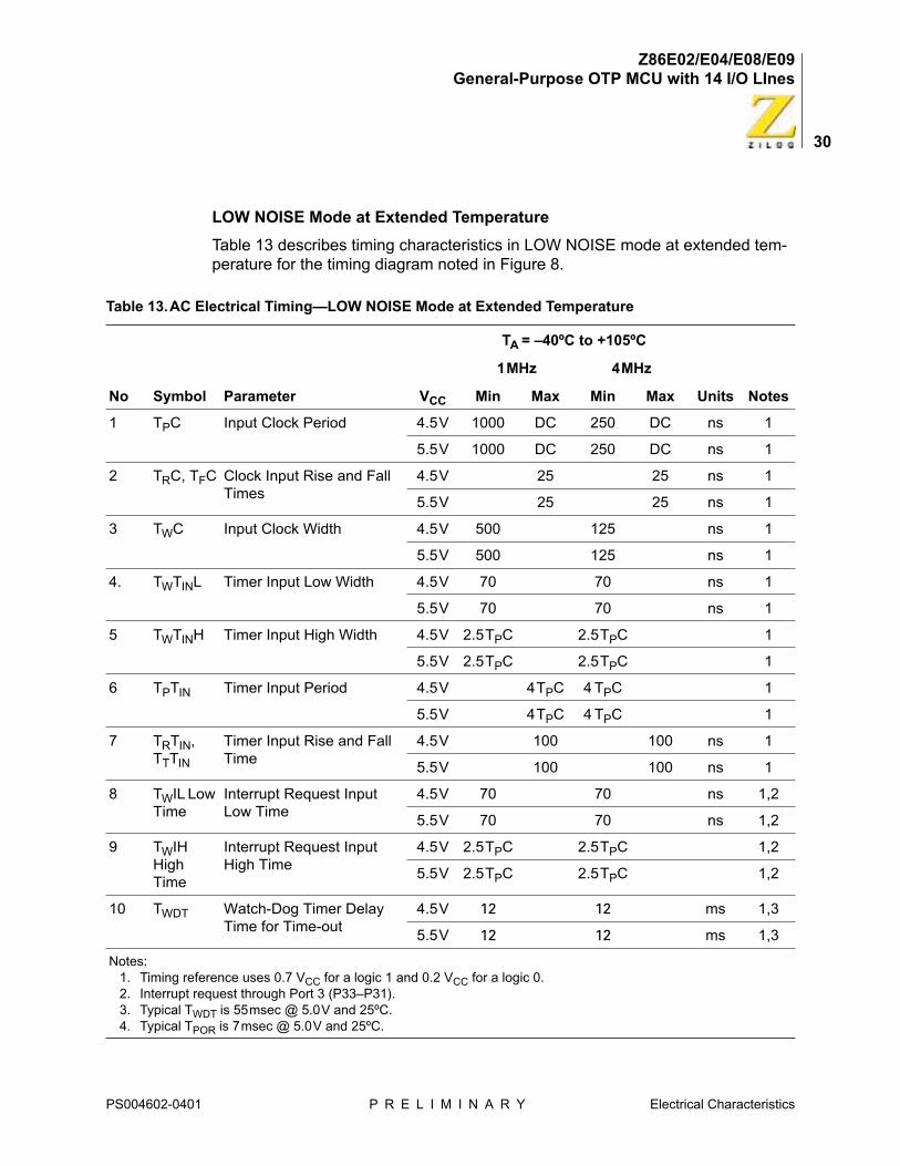
Table 13 describes timing characteristics in LOW NOISE mode at extended tem-perature for the timing diagram noted in Figure 8.
Table 13.AC Electrical Timing—LOW NOISE Mode at Extended Temperature
No Symbol Parameter VCC
TA = –40ºC to +105ºC
Units Notes
1MHz 4MHz
Min Max Min Max
1 TPC Input Clock Period 4.5V 1000 DC 250 DC ns 1
5.5V 1000 DC 250 DC ns 1
2 TRC, TFC Clock Input Rise and Fall Times
4.5V 25 25 ns 1
5.5V 25 25 ns 1
3 TWC Input Clock Width 4.5V 500 125 ns 1
5.5V 500 125 ns 1
4. TWTINL Timer Input Low Width 4.5V 70 70 ns 1
5.5V 70 70 ns 1
5 TWTINH Timer Input High Width 4.5V 2.5TPC 2.5TPC 1
5.5V 2.5TPC 2.5TPC 1
6 TPTIN Timer Input Period 4.5V 4TPC 4 TPC 1
5.5V 4TPC 4 TPC 1
7 TRTIN, TTTIN
Timer Input Rise and Fall Time
4.5V 100 100 ns 1
5.5V 100 100 ns 1
8 TWIL Low Time
Interrupt Request Input Low Time
4.5V 70 70 ns 1,2
5.5V 70 70 ns 1,2
9 TWIH High Time
Interrupt Request Input High Time
4.5V 2.5TPC 2.5TPC 1,2
5.5V 2.5TPC 2.5TPC 1,2
10 TWDT Watch-Dog Timer Delay Time for Time-out
4.5V 12 12 ms 1,3
5.5V 12 12 ms 1,3
Notes: 1. Timing reference uses 0.7 VCC for a logic 1 and 0.2 VCC for a logic 0.2. Interrupt request through Port 3 (P33–P31).3. Typical TWDT is 55msec @ 5.0V and 25ºC.4. Typical TPOR is 7msec @ 5.0V and 25ºC.
PS004602-0401 P R E L I M I N A R Y Electrical Characteristics
Z86E02/E04/E08/E09General-Purpose OTP MCU with 14 I/O LInes
31
Low-Noise Version
Low-EMI Emission
The device can be programmed to operate in a LOW EMI EMISSION mode by means of an OTP bit option. Use of this feature results in:
• All pre-driver slew rates reduced to 10 ns typical
• Internal SCLK and TCLK operation limited to a maximum of 4 MHz–250 ns cycle time
• Output drivers typically exhibit resistances of 500Ω
• Oscillator divide-by-two circuitry eliminated
The LOW EMI mode is an OPT option bit that can be selected by the customer at the time the ROM code is programmed into the OTP EPROM. The default condi-tion is a disabled LOW EMI mode.
11 TPOR Power-On Reset Time 4.5V 2 25 2 25 ms 1,4
5.5V 2 25 2 25 ms 1,4
Table 13.AC Electrical Timing—LOW NOISE Mode at Extended Temperature (Continued)
No Symbol Parameter VCC
TA = –40ºC to +105ºC
Units Notes
1MHz 4MHz
Min Max Min Max
Notes: 1. Timing reference uses 0.7 VCC for a logic 1 and 0.2 VCC for a logic 0.2. Interrupt request through Port 3 (P33–P31).3. Typical TWDT is 55msec @ 5.0V and 25ºC.4. Typical TPOR is 7msec @ 5.0V and 25ºC.
PS004602-0401 P R E L I M I N A R Y Electrical Characteristics
Z86E02/E04/E08/E09General-Purpose OTP MCU with 14 I/O LInes
32
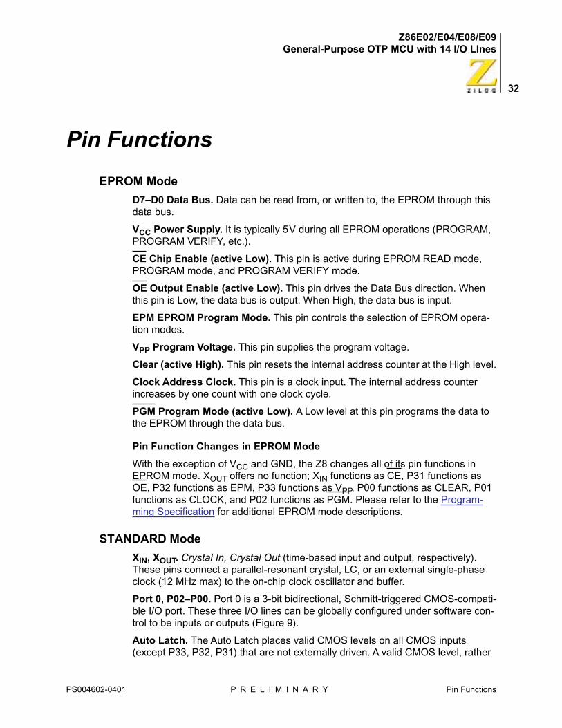
Pin Functions
EPROM Mode
D7–D0 Data Bus. Data can be read from, or written to, the EPROM through this data bus.
VCC Power Supply. It is typically 5V during all EPROM operations (PROGRAM, PROGRAM VERIFY, etc.).
CE Chip Enable (active Low). This pin is active during EPROM READ mode, PROGRAM mode, and PROGRAM VERIFY mode.
OE Output Enable (active Low). This pin drives the Data Bus direction. When this pin is Low, the data bus is output. When High, the data bus is input.
EPM EPROM Program Mode. This pin controls the selection of EPROM opera-tion modes.
VPP Program Voltage. This pin supplies the program voltage.
Clear (active High). This pin resets the internal address counter at the High level.
Clock Address Clock. This pin is a clock input. The internal address counter increases by one count with one clock cycle.
PGM Program Mode (active Low). A Low level at this pin programs the data to the EPROM through the data bus.
Pin Function Changes in EPROM Mode
With the exception of VCC and GND, the Z8 changes all of its pin functions in EPROM mode. XOUT offers no function; XIN functions as CE, P31 functions as OE, P32 functions as EPM, P33 functions as VPP, P00 functions as CLEAR, P01 functions as CLOCK, and P02 functions as PGM. Please refer to the Program-ming Specification for additional EPROM mode descriptions.
STANDARD Mode
XIN, XOUT. Crystal In, Crystal Out (time-based input and output, respectively). These pins connect a parallel-resonant crystal, LC, or an external single-phase clock (12 MHz max) to the on-chip clock oscillator and buffer.
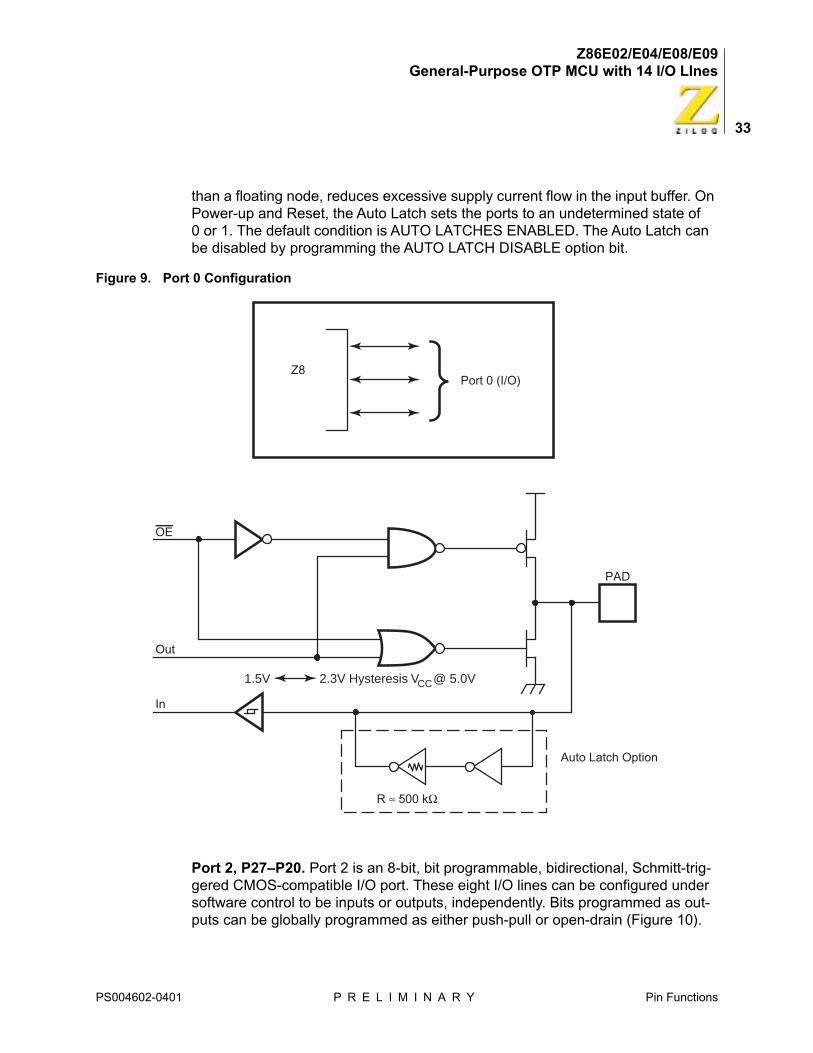
Port 0, P02–P00. Port 0 is a 3-bit bidirectional, Schmitt-triggered CMOS-compati-ble I/O port. These three I/O lines can be globally configured under software con-trol to be inputs or outputs (Figure 9).
Auto Latch. The Auto Latch places valid CMOS levels on all CMOS inputs (except P33, P32, P31) that are not externally driven. A valid CMOS level, rather
PS004602-0401 P R E L I M I N A R Y Pin Functions
Z86E02/E04/E08/E09General-Purpose OTP MCU with 14 I/O LInes
33
than a floating node, reduces excessive supply current flow in the input buffer. On Power-up and Reset, the Auto Latch sets the ports to an undetermined state of 0 or 1. The default condition is AUTO LATCHES ENABLED. The Auto Latch can be disabled by programming the AUTO LATCH DISABLE option bit.
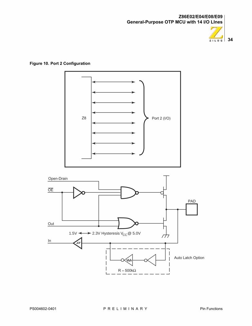
Port 2, P27–P20. Port 2 is an 8-bit, bit programmable, bidirectional, Schmitt-trig-gered CMOS-compatible I/O port. These eight I/O lines can be configured under software control to be inputs or outputs, independently. Bits programmed as out-puts can be globally programmed as either push-pull or open-drain (Figure 10).
Figure 9. Port 0 Configuration
OE
Out
In
PAD
Port 0 (I/O) Z8
Auto Latch Option
R ≈ 500 kΩ
1.5V 2.3V Hysteresis V @ 5.0VCC
PS004602-0401 P R E L I M I N A R Y Pin Functions
Z86E02/E04/E08/E09General-Purpose OTP MCU with 14 I/O LInes
34
Figure 10. Port 2 Configuration
Open-Drain
Out
In
PAD
Port 2 (I/O)
Auto Latch Option
Z8
OE
R ≈ 500kΩ
1.5V 2.3V Hysteresis V @ 5.0VCC
PS004602-0401 P R E L I M I N A R Y Pin Functions
Z86E02/E04/E08/E09General-Purpose OTP MCU with 14 I/O LInes
35
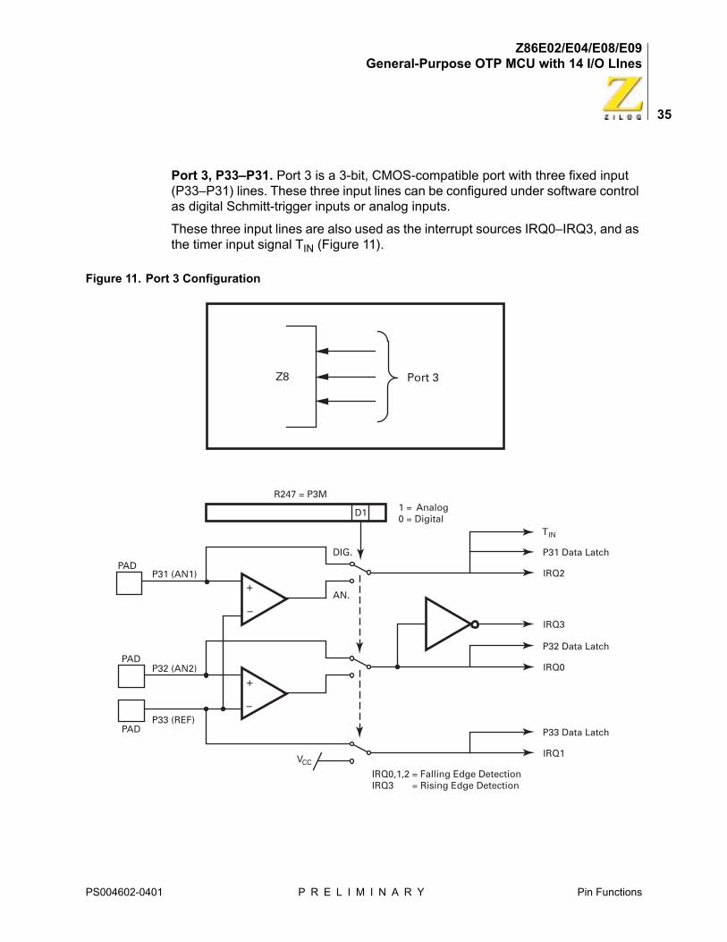
Port 3, P33–P31. Port 3 is a 3-bit, CMOS-compatible port with three fixed input (P33–P31) lines. These three input lines can be configured under software control as digital Schmitt-trigger inputs or analog inputs.
These three input lines are also used as the interrupt sources IRQ0–IRQ3, and as the timer input signal TIN (Figure 11).
Figure 11. Port 3 Configuration
D1
R247 = P3M
P31 (AN1)
P32 (AN2)
1 = Analog0 = Digital
P31 Data Latch
IRQ2
P32 Data Latch
IRQ0
P33 Data Latch
IRQ1
IRQ3
T
DIG.
AN.+
–
+
–
Port 3Z8
V
IRQ0,1,2 = Falling Edge DetectionIRQ3 = Rising Edge Detection
PAD
PAD
PADP33 (REF)
CC
IN
PS004602-0401 P R E L I M I N A R Y Pin Functions
Z86E02/E04/E08/E09General-Purpose OTP MCU with 14 I/O LInes
36
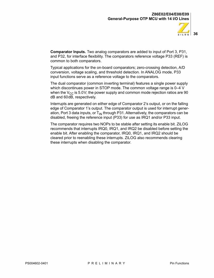
Comparator Inputs. Two analog comparators are added to input of Port 3, P31, and P32, for interface flexibility. The comparators reference voltage P33 (REF) is common to both comparators.
Typical applications for the on-board comparators; zero-crossing detection, A/D conversion, voltage scaling, and threshold detection. In ANALOG mode, P33 input functions serve as a reference voltage to the comparators.
The dual comparator (common inverting terminal) features a single power supply which discontinues power in STOP mode. The common voltage range is 0–4 V when the VCC is 5.0V; the power supply and common mode rejection ratios are 90 dB and 60dB, respectively.
Interrupts are generated on either edge of Comparator 2’s output, or on the falling edge of Comparator 1’s output. The comparator output is used for interrupt gener-ation, Port 3 data inputs, or TIN through P31. Alternatively, the comparators can be disabled, freeing the reference input (P33) for use as IRQ1 and/or P33 input.
The comparator requires two NOPs to be stable after setting its enable bit. ZiLOG recommends that interrupts IRQ0, IRQ1, and IRQ2 be disabled before setting the enable bit. After enabling the comparator, IRQ0, IRQ1, and IRQ2 should be cleared prior to reenabling these interrupts. ZiLOG also recommends clearing these interrupts when disabling the comparator.
PS004602-0401 P R E L I M I N A R Y Pin Functions
Z86E02/E04/E08/E09General-Purpose OTP MCU with 14 I/O LInes
37
Functional Description
The following special functions are incorporated into the Z8 devices to enhance the standard Z8 core architecture and to provide the user with increased design flexibility.
RESET
A RESET can be triggered in the following two ways:
• Power-On Reset
• Watch-Dog Timer Reset
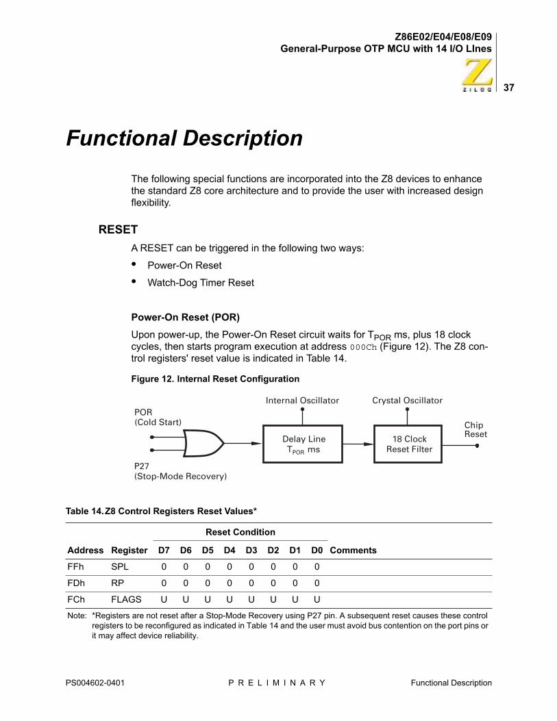
Power-On Reset (POR)
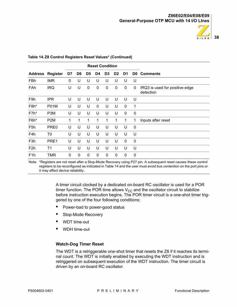
Upon power-up, the Power-On Reset circuit waits for TPOR ms, plus 18 clock cycles, then starts program execution at address 000Ch (Figure 12). The Z8 con-trol registers' reset value is indicated in Table 14.
Figure 12. Internal Reset Configuration
Table 14.Z8 Control Registers Reset Values*
Address Register
Reset Condition
CommentsD7 D6 D5 D4 D3 D2 D1 D0
FFh SPL 0 0 0 0 0 0 0 0
FDh RP 0 0 0 0 0 0 0 0
FCh FLAGS U U U U U U U U
Note: *Registers are not reset after a Stop-Mode Recovery using P27 pin. A subsequent reset causes these control registers to be reconfigured as indicated in Table 14 and the user must avoid bus contention on the port pins or it may affect device reliability.
POR(Cold Start)
P27(Stop-Mode Recovery)
Delay LineTPOR ms
18 ClockReset Filter
Crystal OscillatorInternal Oscillator
ChipReset
PS004602-0401 P R E L I M I N A R Y Functional Description
Z86E02/E04/E08/E09General-Purpose OTP MCU with 14 I/O LInes
38
A timer circuit clocked by a dedicated on-board RC oscillator is used for a POR timer function. The POR time allows VCC and the oscillator circuit to stabilize before instruction execution begins. The POR timer circuit is a one-shot timer trig-gered by one of the four following conditions:
• Power-bad to power-good status
• Stop-Mode Recovery
• WDT time-out
• WDH time-out
Watch-Dog Timer Reset
The WDT is a retriggerable one-shot timer that resets the Z8 if it reaches its termi-nal count. The WDT is initially enabled by executing the WDT instruction and is retriggered on subsequent execution of the WDT instruction. The timer circuit is driven by an on-board RC oscillator.
FBh IMR 0 U U U U U U U
FAh IRQ U U 0 0 0 0 0 0 IRQ3 is used for positive edge detection
F9h IPR U U U U U U U U
F8h* P01M U U U 0 U U 0 1
F7h* P3M U U U U U U 0 0
F6h* P2M 1 1 1 1 1 1 1 1 Inputs after reset
F5h PRE0 U U U U U U U 0
F4h T0 U U U U U U U U
F3h PRE1 U U U U U U 0 0
F2h T1 U U U U U U U U
F1h TMR 0 0 0 0 0 0 0 0
Table 14.Z8 Control Registers Reset Values* (Continued)
Address Register
Reset Condition
CommentsD7 D6 D5 D4 D3 D2 D1 D0
Note: *Registers are not reset after a Stop-Mode Recovery using P27 pin. A subsequent reset causes these control registers to be reconfigured as indicated in Table 14 and the user must avoid bus contention on the port pins or it may affect device reliability.
PS004602-0401 P R E L I M I N A R Y Functional Description
Z86E02/E04/E08/E09General-Purpose OTP MCU with 14 I/O LInes
39
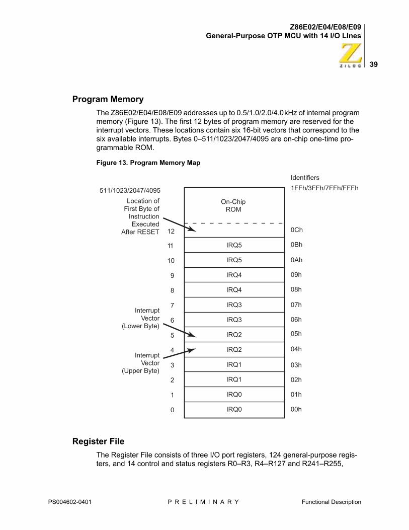
Program Memory
The Z86E02/E04/E08/E09 addresses up to 0.5/1.0/2.0/4.0kHz of internal program memory (Figure 13). The first 12 bytes of program memory are reserved for the interrupt vectors. These locations contain six 16-bit vectors that correspond to the six available interrupts. Bytes 0–511/1023/2047/4095 are on-chip one-time pro-grammable ROM.
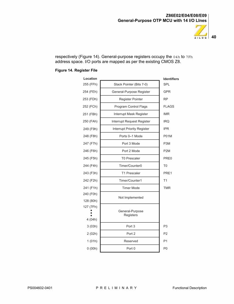
Register File
The Register File consists of three I/O port registers, 124 general-purpose regis-ters, and 14 control and status registers R0–R3, R4–R127 and R241–R255,
Figure 13. Program Memory Map
12
11
10
9
8
7
6
5
4
3
2
1
0
Location ofFirst Byte of
InstructionExecuted
After RESET
InterruptVector
(Lower Byte)
InterruptVector
(Upper Byte)
IRQ5
IRQ4
IRQ4
IRQ3
IRQ3
IRQ2
IRQ2
IRQ1
IRQ1
IRQ0
IRQ0
IRQ5
On-ChipROM
511/1023/2047/4095 1FFh/3FFh/7FFh/FFFh
0Ch
0Bh
0Ah
09h
08h
07h
06h
05h
04h
03h
02h
01h
00h
Identifiers
PS004602-0401 P R E L I M I N A R Y Functional Description
Z86E02/E04/E08/E09General-Purpose OTP MCU with 14 I/O LInes
40
respectively (Figure 14). General-purpose registers occupy the 04h to 7Fh address space. I/O ports are mapped as per the existing CMOS Z8.
Figure 14. Register File
SPLStack Pointer (Bits 7-0)
General-Purpose Register
Register Pointer
Program Control Flags
Interrupt Mask Register
Interrupt Request Register
Interrupt Priority Register
Ports 0–1 Mode
Port 3 Mode
Port 2 Mode
T0 Prescaler
Timer/Counter0
T1 Prescaler
Timer/Counter1
Timer Mode
Not Implemented
General-PurposeRegisters
Port 3
Port 2
Reserved
Port 0
RP
IMR
IRQ
IPR
P3M
P2M
PRE0
T0
PRE1
T1
TMR
P3
P2
P1
P0
P01M
FLAGS
Location
255 (FFh)
254 (FEh)
253 (FDh)
252 (FCh)
251 (FBh)
250 (FAh)
249 (F9h)
248 (F8h)
247 (F7h)
246 (F6h)
245 (F5h)
244 (F4h)
243 (F3h)
242 (F2h)
241 (F1h)
4 (04h)
3 (03h)
2 (02h)
1 (01h)
128 (80h)
240 (F0h)
127 (7Fh)
GPR
Identifiers
0 (00h)
•••
PS004602-0401 P R E L I M I N A R Y Functional Description
Z86E02/E04/E08/E09General-Purpose OTP MCU with 14 I/O LInes
41
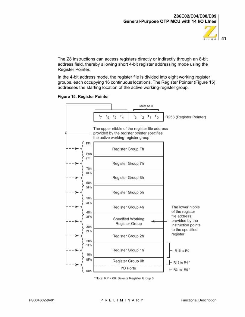
The Z8 instructions can access registers directly or indirectly through an 8-bit address field, thereby allowing short 4-bit register addressing mode using the Register Pointer.
In the 4-bit address mode, the register file is divided into eight working register groups, each occupying 16 continuous locations. The Register Pointer (Figure 15) addresses the starting location of the active working-register group.
Figure 15. Register Pointer
The upper nibble of the register file addressprovided by the register pointer specifiesthe active working-register group
r7 r6 r5 r4 R253 (Register Pointer)
I/O Ports
Specified WorkingRegister Group
The lower nibbleof the registerfile addressprovided by theinstruction pointsto the specifiedregister
r3 r2 r1 r0
Register Group 0h
7Fh
Register Group 1h
Register Group 2h
Register Group 4h
Register Group 5h
Register Group 6h
Register Group 7h
Register Group Fh
6Fh
5Fh
4Fh
3Fh
2Fh
1Fh
0Fh
00h
10h
20h
30h
40h
50h
60h
70h
FFh
F0h
R15 to R0
R15 to R4 *
R3 to R0 *
*Note: RP = 00: Selects Register Group 0.
Must be 0
PS004602-0401 P R E L I M I N A R Y Functional Description
Z86E02/E04/E08/E09General-Purpose OTP MCU with 14 I/O LInes
42
Stack Pointer
The Z8 features an 8-bit Stack Pointer (R255) used for the internal stack that resides within the 120 general-purpose registers from 04h to 7Fh.
General-Purpose Registers (GPR)
These registers are undefined after the device is powered up. The registers keep their most recent value after any reset, as long as the reset occurs in the VCC volt-age-specified operating range.
Register R254 is designated as a general-purpose register andis set to 00h after any reset or Stop-Mode Recovery.
Counter/Timer
There are two 8-bit programmable counter/timers (T0 and T1), each driven by its own 6-bit programmable prescaler. The T1 prescaler is driven by internal or exter-nal clock sources; however, the T0 can be driven by the internal clock source only (Figure 16).
The 6-bit prescalers divide the input frequency of the clock source by any integer number from 1 to 64. Each prescaler drives its counter, which decrements the value (1 to 256) that is loaded into the counter. When both counter and prescaler reach the end of count, a timer interrupt request IRQ4 (T0) or IRQ5 (T1) is gener-ated.
The counter can be programmed to start, stop, restart to continue, or restart from the initial value. The counters are also programmed to stop upon reaching zero (SINGLE-PASS mode) or to automatically reload the initial value and continue counting (MODULO-N CONTINUOUS mode).
The counters, but not the prescalers, are read at any time without disturbing their value or count mode. The clock source for T1 is user-definable and is either the internal microprocessor clock divided by four, or an external signal input through Port 3. The TIMER mode register configures the external timer input (P31) as an external clock, a trigger input that is retriggerable or nonretriggerable, or used as a gate input for the internal clock.
This step is bypassed if LOW EMI mode is selected.
Note:
Note:
PS004602-0401 P R E L I M I N A R Y Functional Description

Z86E02/E04/E08/E09General-Purpose OTP MCU with 14 I/O LInes
43
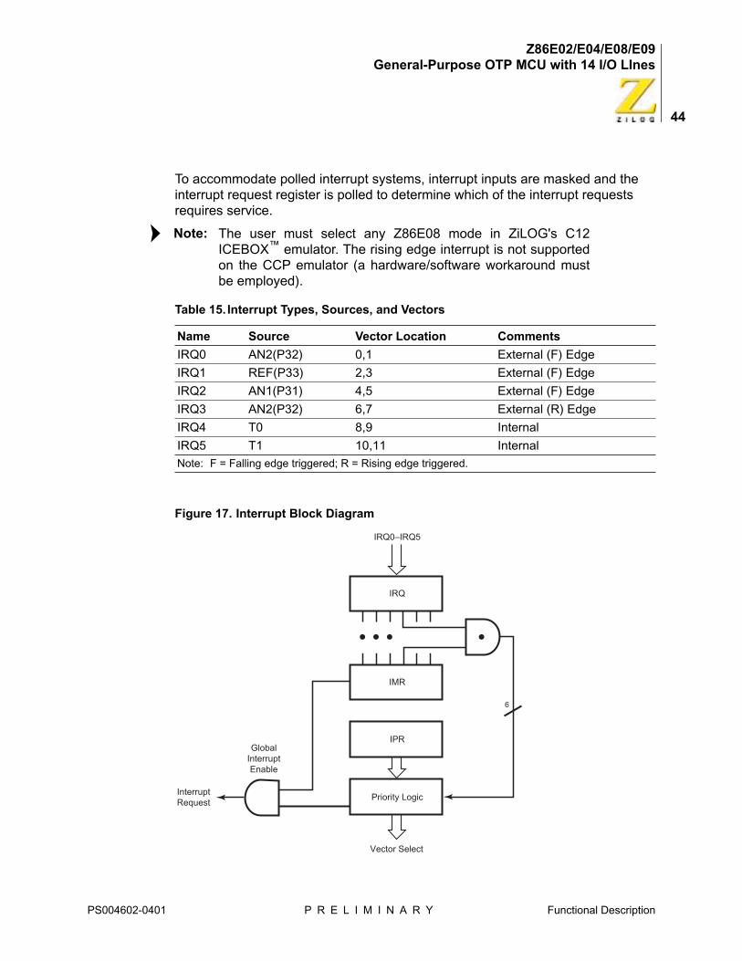
Interrupts
The Z8 features six interrupts from six different sources. These interrupts are maskable and prioritized (Figure 17). The sources are divided as follows: the fall-ing edge of P31 (AN1), P32 (AN2), P33 (REF), the rising edge of P32 (AN2), and two counter/timers. The Interrupt Mask Register globally or individually enables or disables the six interrupt requests (Table 15).
When more than one interrupt is pending, priorities are resolved by a programma-ble priority encoder that is controlled by the Interrupt Priority register. All Z8 inter-rupts are vectored through locations in program memory. When an interrupt machine cycle is activated, an Interrupt Request is granted, thus disabling all sub-sequent interrupts, saving the Program Counter and Status Flags, and then branching to the program memory vector location reserved for that interrupt. This memory location and the next byte contain the 16-bit starting address of the inter-rupt service routine for that particular interrupt request.
Figure 16. Counter/Timers Block Diagram
OSC
÷4
6-BitDowncounter
÷2
÷4
ClockLogic IRQ5
Internal Data Bus
ReadWriteWrite
ReadWriteWrite
Internal ClockGated ClockTriggered Clock
T P31
External Clock
Internal Clock
*
8-BitDowncounter
T1Current Value
Register
T1Initial Value
Register
PRE1Initial Value
Register
6-BitDowncounter IRQ4
Internal Data Bus
8-BitDowncounter
T0Current Value
Register
T0Initial Value
Register
PRE0Initial Value
Register
IN
PS004602-0401 P R E L I M I N A R Y Functional Description
Z86E02/E04/E08/E09General-Purpose OTP MCU with 14 I/O LInes
44
To accommodate polled interrupt systems, interrupt inputs are masked and the interrupt request register is polled to determine which of the interrupt requests requires service.
The user must select any Z86E08 mode in ZiLOG's C12ICEBOX™ emulator. The rising edge interrupt is not supportedon the CCP emulator (a hardware/software workaround mustbe employed).
Table 15. Interrupt Types, Sources, and Vectors
Name Source Vector Location Comments
IRQ0 AN2(P32) 0,1 External (F) Edge
IRQ1 REF(P33) 2,3 External (F) Edge
IRQ2 AN1(P31) 4,5 External (F) Edge
IRQ3 AN2(P32) 6,7 External (R) Edge
IRQ4 T0 8,9 Internal
IRQ5 T1 10,11 Internal
Note: F = Falling edge triggered; R = Rising edge triggered.
Figure 17. Interrupt Block Diagram
Note:
IRQ0–IRQ5
IRQ
IMR
IPR
Priority Logic
GlobalInterruptEnable
InterruptRequest
Vector Select
6
PS004602-0401 P R E L I M I N A R Y Functional Description
Z86E02/E04/E08/E09General-Purpose OTP MCU with 14 I/O LInes
45
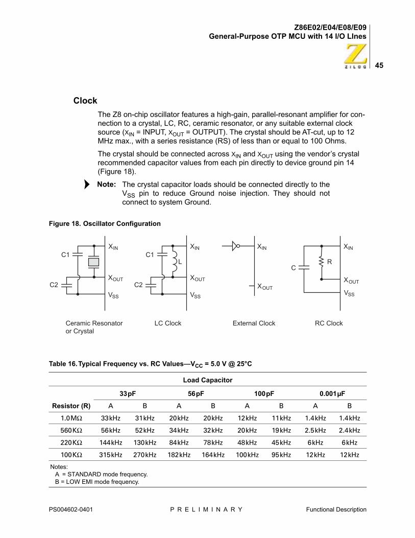
Clock
The Z8 on-chip oscillator features a high-gain, parallel-resonant amplifier for con-nection to a crystal, LC, RC, ceramic resonator, or any suitable external clock source (XIN = INPUT, XOUT = OUTPUT). The crystal should be AT-cut, up to 12 MHz max., with a series resistance (RS) of less than or equal to 100 Ohms.
The crystal should be connected across XIN and XOUT using the vendor’s crystal recommended capacitor values from each pin directly to device ground pin 14 (Figure 18).
The crystal capacitor loads should be connected directly to theVSS pin to reduce Ground noise injection. They should notconnect to system Ground.
Figure 18. Oscillator Configuration
Table 16.Typical Frequency vs. RC Values—VCC = 5.0 V @ 25°C
Load Capacitor
Resistor (R)
33pF 56pF 100pF 0.001µF
A B A B A B A B
1.0MΩ 33kHz 31kHz 20kHz 20kHz 12kHz 11kHz 1.4kHz 1.4kHz
560KΩ 56kHz 52kHz 34kHz 32kHz 20kHz 19kHz 2.5kHz 2.4kHz
220KΩ 144kHz 130kHz 84kHz 78kHz 48kHz 45kHz 6kHz 6kHz
100KΩ 315kHz 270kHz 182kHz 164kHz 100kHz 95kHz 12kHz 12kHz
Notes: A = STANDARD mode frequency.B = LOW EMI mode frequency.
Note:
X
X
C1 C1
C2 C2
Ceramic Resonatoror Crystal
External Clock
L
LC Clock
X X
X
X
X
R
RC Clock
C
IN IN IN IN
OUT
VSS
XOUT
VSSVSS
OUTOUT
PS004602-0401 P R E L I M I N A R Y Functional Description
Z86E02/E04/E08/E09General-Purpose OTP MCU with 14 I/O LInes
46
HALT Mode
This instruction turns off the internal CPU clock but not the crystal oscillation. The counter/timers and external interrupts IRQ0, IRQ1, IRQ2 and IRQ3 remain active.
56KΩ 552kHz 480kHz 330kHz 300kHz 185kHz 170kHz 23kHz 22kHz
20KΩ 1.4MHz 1MHz 884kHz 740kHz 500kHz 450kHz 65kHz 61kHz
10KΩ 2.6MHz 2MHz 1.6MHz 1.3MHz 980kHz 820kHz 130kHz 123kHz
5KΩ 4.4MHz 3MHz 2.8MHz 2MHz 1.7MHz 1.3MHz 245kHz 225kHz
2KΩ 8MHz 5MHz 6MHz 4MHz 3.8MHz 2.7MHz 600kHz 536kHz
1KΩ 12MHz 7MHz 8.8MHz 6MHz 6.3MHz 4.2MHz 1.0MHz 950kHz
Table 17.Typical Frequency vs. RC Values—VCC = 3.3 V @ 25°C
Load Capacitor
Resistor (R)
33 pF 56 pF 100 pF 0.00 1µF
A B A B A B A B
1.0MΩ 18 kHz 18 kHz 12 kHz 12 kHz 7.4 kHz 7.7 kHz 1 kHz 1 kHz
560 KΩ 30 kHz 30 kHz 20 kHz 20 kHz 12 kHz 12 kHz 1.6 kHz 1.6 kHz
220KΩ 70kHz 70kHz 47kHz 47kHz 30kHz 30kHz 4kHz 4kHz
100KΩ 150kHz 148kHz 97kHz 96kHz 60kHz 60kHz 8kHz 8kHz
56KΩ 268kHz 250kHz 176kHz 170kHz 100kHz 100kHz 15kHz 15kHz
20KΩ 690MHz 600kHz 463kHz 416kHz 286kHz 266kHz 40kHz 40kHz
10KΩ 1.2MHz 1MHz 860kHz 730kHz 540kHz 480kHz 80kHz 76kHz
5KΩ 2MHz 1.7MHz 1.5MHz 1.2MHz 950kHz 820kHz 151kHz 138kHz
2KΩ 4.6MHz 3MHz 3.3MHz 2.4MHz 2.2MHz 1.6MHz 360kHz 316kHz
1KΩ 7MHz 4.6MHz 5MHz 3.6MHz 3.6MHz 2.6MHz 660kHz 565kHz
Notes: A = STANDARD mode frequency.B = LOW EMI MODE frequency.
Table 16.Typical Frequency vs. RC Values—VCC = 5.0 V @ 25°C (Continued)
Load Capacitor
Notes: A = STANDARD mode frequency.B = LOW EMI mode frequency.
PS004602-0401 P R E L I M I N A R Y Functional Description
Z86E02/E04/E08/E09General-Purpose OTP MCU with 14 I/O LInes
47
The device is recovered by interrupts, either externally or internally generated. An interrupt request must be executed (enabled) to exit HALT mode. After the inter-rupt service routine, the program continues from the instruction after the HALT.
On the C12 ICEBOX, the IRQ3 does not wake the device out ofHALT mode.
STOP Mode
This instruction turns off the internal clock and external crystal oscillation and reduces the standby current to 10 µA. The STOP mode is released by a RESET through a Stop-Mode Recovery (pin P27). A LOW INPUT condition on P27 releases the STOP mode. Program execution begins at location 000C(Hex). How-ever, when P27 is used to release STOP mode, the I/O port mode registers are not reconfigured to their default POWER-ON conditions. Thus the I/O, configured as output when the STOP instruction was executed, is prevented from glitching to an unknown state. To use the P27 release approach with STOP mode, use the fol-lowing instruction:
A Low level detected on pin P27 takes the device out of STOPmode, even if it is configured as an output.
To enter STOP or HALT mode, it is necessary to first flush the instruction pipeline to avoid suspending execution in mid-instruction. The user must execute a NOP (Op Code = FFh) immediately before the appropriate SLEEP instruction, such as:
On the CCP emulator, a software workaround must be used toenable P27 as the Stop-Mode Recovery source.
LD P2M, #1XXX XXXXB
NOP
STOP
Note: X = Dependent on user's application.
FFh NOP ; clear the pipeline
6Fh STOP ; enter STOP mode
or
FFh NOP ; clear the pipeline
7Fh HALT ; enter HALT mode
Note:
Note:
Note:
PS004602-0401 P R E L I M I N A R Y Functional Description
Z86E02/E04/E08/E09General-Purpose OTP MCU with 14 I/O LInes
48
Watch-Dog Timer (WDT)
The Watch-Dog Timer is enabled by instruction WDT. When the WDT is enabled, it cannot be stopped by the instruction. With the WDT instruction, the WDT is refreshed when it is enabled within every 1 TWDT period; otherwise, the controller resets itself, The WDT instruction affects the flags accordingly; Z = 1, S = 0, V = 0.
WDT = 5Fh
Op Code WDT (5Fh)
The first time Op Code 5Fh is executed, the WDT is enabled; subsequent execu-tion clears the WDT counter. This clearing of the counter must be performed at least every TWDT; otherwise, the WDT times out and generates a reset. The gen-erated reset is the same as a power-on reset of TPOR, plus 18 crystal clock cycles. The software enabled WDT does not run in STOP mode.
Op Code WDH (4Fh)
When this instruction is executed it enables the WDT during HALT. If not, the WDT stops when entering HALT. This instruction does not clear the counters—it just makes it possible to operate the WDT during HALT mode. A WDH instruction exe-cuted without executing WDT (5Fh) yields no effect.
Permanent WDT
Selecting the hardware-enabled Permanent WDT option bit automatically enables the WDT upon exiting reset. The permanent WDT always runs in HALT mode and STOP mode, and it cannot be disabled.
On the CCP emulator, a software workaround must be used toenable the software- or hardware-enabled WDT.
Auto Reset Voltage (VLV)
The Z8 features an auto-reset built-in. The auto-reset circuit resets the Z8 when it detects the VCC below VLV. Figure 19 shows the Auto Reset Voltage versus tem-perature. If the VCC drops below the VCC operating voltage range, the Z8 functions down to the VLV unless the internal clock frequency is higher than the specified maximum VLV frequency.
Note:
PS004602-0401 P R E L I M I N A R Y Functional Description

Z86E02/E04/E08/E09General-Purpose OTP MCU with 14 I/O LInes
49
Figure 19. Typical Auto Reset Voltage (VLV) vs. Temperature
Note: (1) applies to VLV in RUN and HALT modes. (2) applies to VLV in STOP mode.
Temp
2.2
2.0
1.9
1.8
1.7-40ºC -20ºC 0ºC 20ºC 40ºC 60ºC 80ºC 100ºC 120ºC
2.1
VCC
(Volts)
2.9
2.7
2.6
2.5
2.4
2.3
2.81
2
PS004602-0401 P R E L I M I N A R Y Functional Description
Z86E02/E04/E08/E09General-Purpose OTP MCU with 14 I/O LInes
PS004602-0401 P R E L I M I N A R Y OTP Option Bit Description
50
OTP Option Bit Description
One-Time Programmable EPROM option bits for the device are described in this section.
Low-EMI Emission. The Z8 can be programmed to operate in a low-EMI emis-sion (low-noise) mode by means of an EPROM programmable bit option. Use of this feature results in:
• All drivers slew rates are typically reduced to 10ns
• Internal SCLK and TCLK = crystal operation limited to a maximum of 4 MHz–250 ns cycle time
• Output drivers typically exhibit resistances of 500 ohms
• Oscillator divide-by-two circuitry eliminated
RC Oscillator. The RC Oscillator option bit, when programmed, enables the inter-nal RC oscillator to connect to the XOUT and XIN pins while disabling the internal crystal oscillator to XOUT and XIN.
ROM Protect. ROM Protect fully protects the Z8 ROM code from being read externally. When ROM Protect is selected, the instructions LDC and LDCI are supported (Z86E02/E04/E08/E09 and Z86C02/C04/C08 do not support the instructions of LDE and LDEI). When the device is programmed for ROM Protect, the Low-Noise feature is not automatically enabled.
Auto Latch Disable. Auto Latch Disable option bit, when programmed, globally disables all Auto Latches.
Permanent WDT Enable. The hardware-enabled permanent WDT Enable option bit, when programmed, enables the WDT permanently after exiting reset. Unlike software-enabled WDT, the hardware-enabled permanent WDT cannot be stopped in HALT or STOP modes.
32-kHz Enable. The 32-kHz Enable option bit enables the 32-kHz oscillator circuit and disables the high-frequency crystal oscillator circuit. This option bit is disabled if the RC oscillator option bit is programmed.
Z86E02/E04/E08/E09General-Purpose OTP MCU with 14 I/O LInes
51
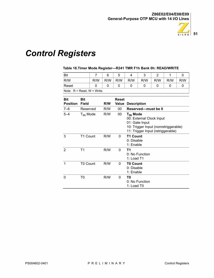
Control Registers
Table 18.Timer Mode Register—R241 TMR F1h Bank 0h: READ/WRITE
Bit 7 6 5 4 3 2 1 0
R/W R/W R/W R/W R/W R/W R/W R/W R/W
Reset 0 0 0 0 0 0 0 0
Note: R = Read, W = Write.
Bit Position
BitField R/W
Reset Value Description
7–6 Reserved R/W 00 Reserved—must be 0
5–4 TIN Mode R/W 00 TIN Mode00: External Clock Input01: Gate Input10: Trigger Input (nonretriggerable)11: Trigger Input (retriggerable)
3 T1 Count R/W 0 T1 Count0: Disable1: Enable
2 T1 R/W 0 T10: No Function1: Load T1
1 T0 Count R/W 0 T0 Count0: Disable1: Enable
0 T0 R/W 0 T00: No Function1: Load T0
PS004602-0401 P R E L I M I N A R Y Control Registers
Z86E02/E04/E08/E09General-Purpose OTP MCU with 14 I/O LInes
52
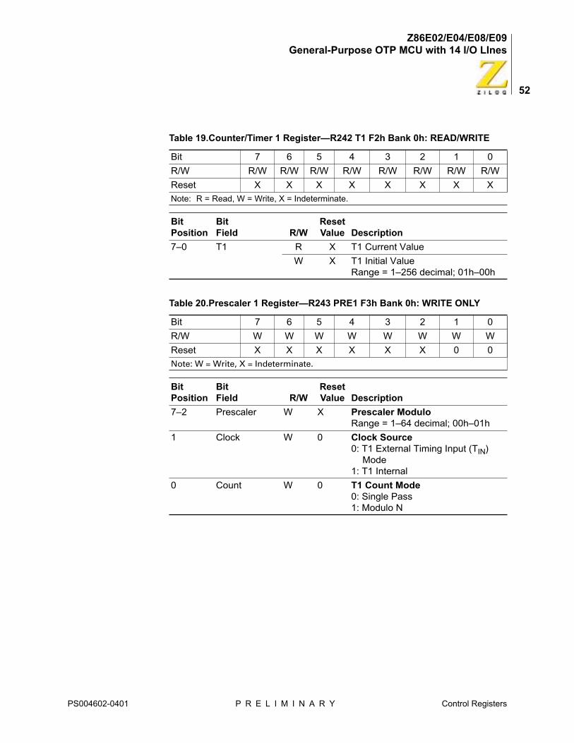
Table 19.Counter/Timer 1 Register—R242 T1 F2h Bank 0h: READ/WRITE
Bit 7 6 5 4 3 2 1 0
R/W R/W R/W R/W R/W R/W R/W R/W R/W
Reset X X X X X X X X
Note: R = Read, W = Write, X = Indeterminate.
Bit Position
Bit Field R/W
Reset Value Description
7–0 T1 R X T1 Current Value
W X T1 Initial ValueRange = 1–256 decimal; 01h–00h
Table 20.Prescaler 1 Register—R243 PRE1 F3h Bank 0h: WRITE ONLY
Bit 7 6 5 4 3 2 1 0
R/W W W W W W W W W
Reset X X X X X X 0 0
Note: W = Write, X = Indeterminate.
Bit Position
Bit Field R/W
Reset Value Description
7–2 Prescaler W X Prescaler ModuloRange = 1–64 decimal; 00h–01h
1 Clock W 0 Clock Source0: T1 External Timing Input (TIN)
Mode1: T1 Internal
0 Count W 0 T1 Count Mode0: Single Pass1: Modulo N
PS004602-0401 P R E L I M I N A R Y Control Registers
Z86E02/E04/E08/E09General-Purpose OTP MCU with 14 I/O LInes
53
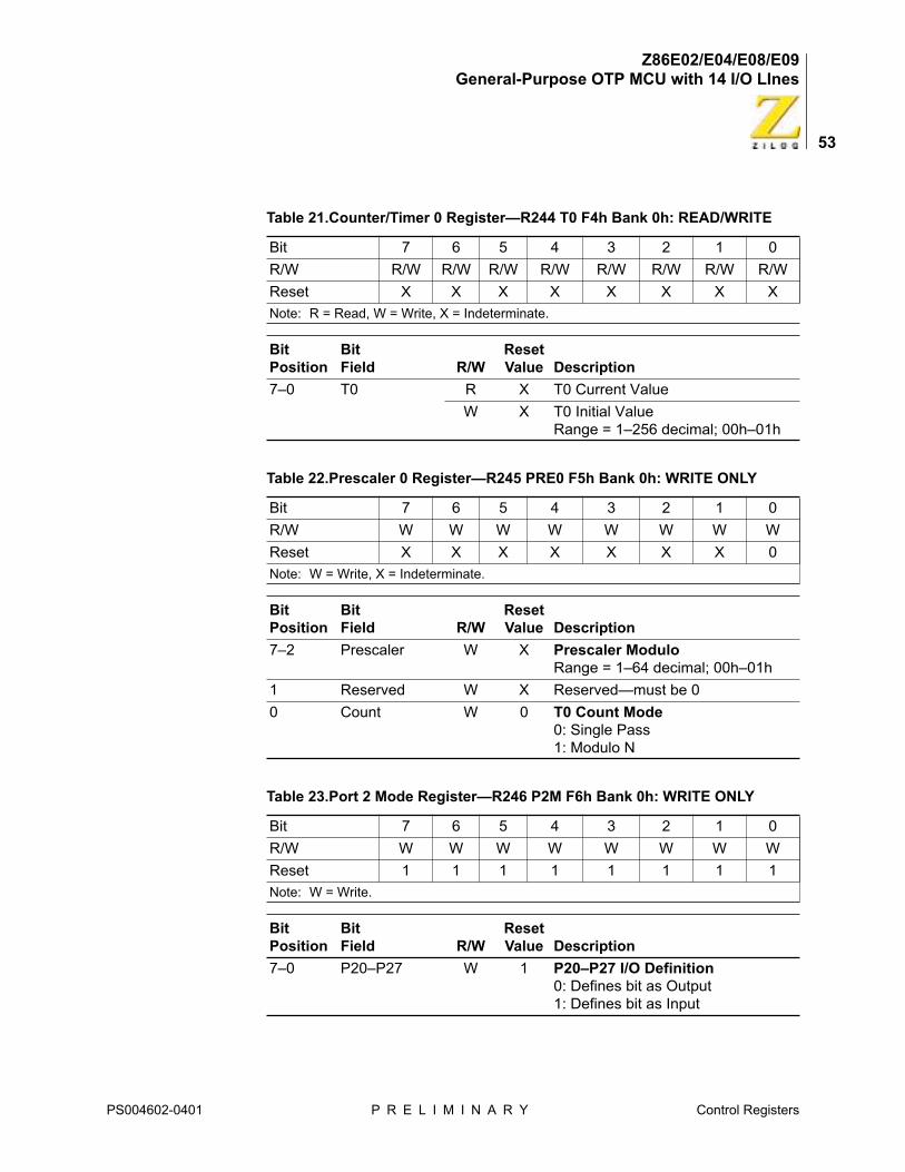
Table 21.Counter/Timer 0 Register—R244 T0 F4h Bank 0h: READ/WRITE
Bit 7 6 5 4 3 2 1 0
R/W R/W R/W R/W R/W R/W R/W R/W R/W
Reset X X X X X X X X
Note: R = Read, W = Write, X = Indeterminate.
Bit Position
Bit Field R/W
Reset Value Description
7–0 T0 R X T0 Current Value
W X T0 Initial ValueRange = 1–256 decimal; 00h–01h
Table 22.Prescaler 0 Register—R245 PRE0 F5h Bank 0h: WRITE ONLY
Bit 7 6 5 4 3 2 1 0
R/W W W W W W W W W
Reset X X X X X X X 0
Note: W = Write, X = Indeterminate.
Bit Position
Bit Field R/W
Reset Value Description
7–2 Prescaler W X Prescaler ModuloRange = 1–64 decimal; 00h–01h
1 Reserved W X Reserved—must be 0
0 Count W 0 T0 Count Mode0: Single Pass1: Modulo N
Table 23.Port 2 Mode Register—R246 P2M F6h Bank 0h: WRITE ONLY
Bit 7 6 5 4 3 2 1 0
R/W W W W W W W W W
Reset 1 1 1 1 1 1 1 1
Note: W = Write.
Bit Position
Bit Field R/W
Reset Value Description
7–0 P20–P27 W 1 P20–P27 I/O Definition0: Defines bit as Output1: Defines bit as Input
PS004602-0401 P R E L I M I N A R Y Control Registers
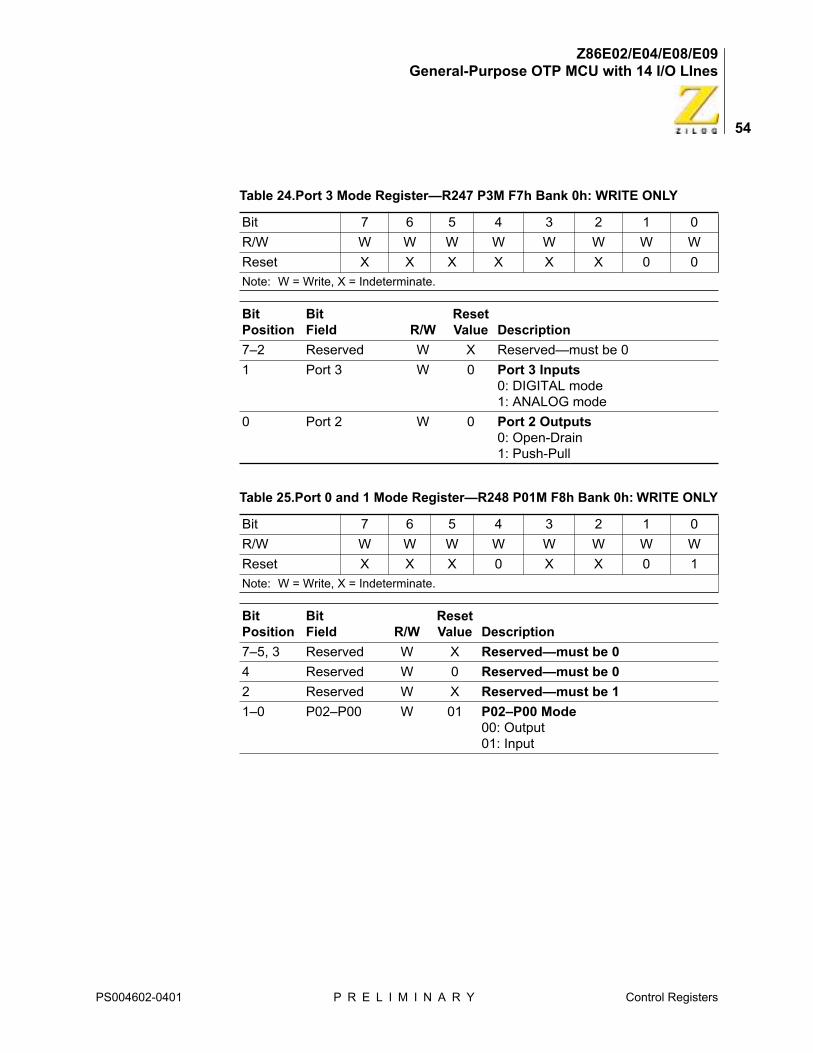
Z86E02/E04/E08/E09General-Purpose OTP MCU with 14 I/O LInes
54
Table 24.Port 3 Mode Register—R247 P3M F7h Bank 0h: WRITE ONLY
Bit 7 6 5 4 3 2 1 0
R/W W W W W W W W W
Reset X X X X X X 0 0
Note: W = Write, X = Indeterminate.
Bit Position
Bit Field R/W
Reset Value Description
7–2 Reserved W X Reserved—must be 0
1 Port 3 W 0 Port 3 Inputs0: DIGITAL mode1: ANALOG mode
0 Port 2 W 0 Port 2 Outputs0: Open-Drain1: Push-Pull
Table 25.Port 0 and 1 Mode Register—R248 P01M F8h Bank 0h: WRITE ONLY
Bit 7 6 5 4 3 2 1 0
R/W W W W W W W W W
Reset X X X 0 X X 0 1
Note: W = Write, X = Indeterminate.
Bit Position
Bit Field R/W
Reset Value Description
7–5, 3 Reserved W X Reserved—must be 0
4 Reserved W 0 Reserved—must be 0
2 Reserved W X Reserved—must be 1
1–0 P02–P00 W 01 P02–P00 Mode00: Output01: Input
PS004602-0401 P R E L I M I N A R Y Control Registers

Z86E02/E04/E08/E09General-Purpose OTP MCU with 14 I/O LInes
55
Table 26.Interrupt Priority Register—R249 IPR F9h Bank 0h: WRITE ONLY
Bit 7 6 5 4 3 2 1 0
R/W W W W W W W W W
Reset X X X X X X X X
Note: W = Write, X = Indeterminate.
Bit Position
Bit Field R/W
Reset Value Description
7–6 Reserved W X Reserved—must be 0
5 IRQ3, IRQ5 W X IRQ3, IRQ5 Priority (Group A)0: IRQ5 > IRQ31: IRQ3 > IRQ5
4,3,0 Interrupt W X Interrupt Group Priority000: Reserved*001: C > A > B010: A > B > C011: A > C > B100: B > C > A101: C > B > A110: B > A > C111: Reserved
2 IRQ0, IRQ2 W X IRQ0, IRQ2 Priority (Group B)0: IRQ2 > IRQ01: IRQ0 > IRQ2
1 IRQ1, IRQ4 W X IRQ1, IRQ4 Priority (Group C)0: IRQ1 > IRQ41: IRQ4 > IRQ1
Note: *Selecting a Reserved mode causes an undefined operation.
PS004602-0401 P R E L I M I N A R Y Control Registers
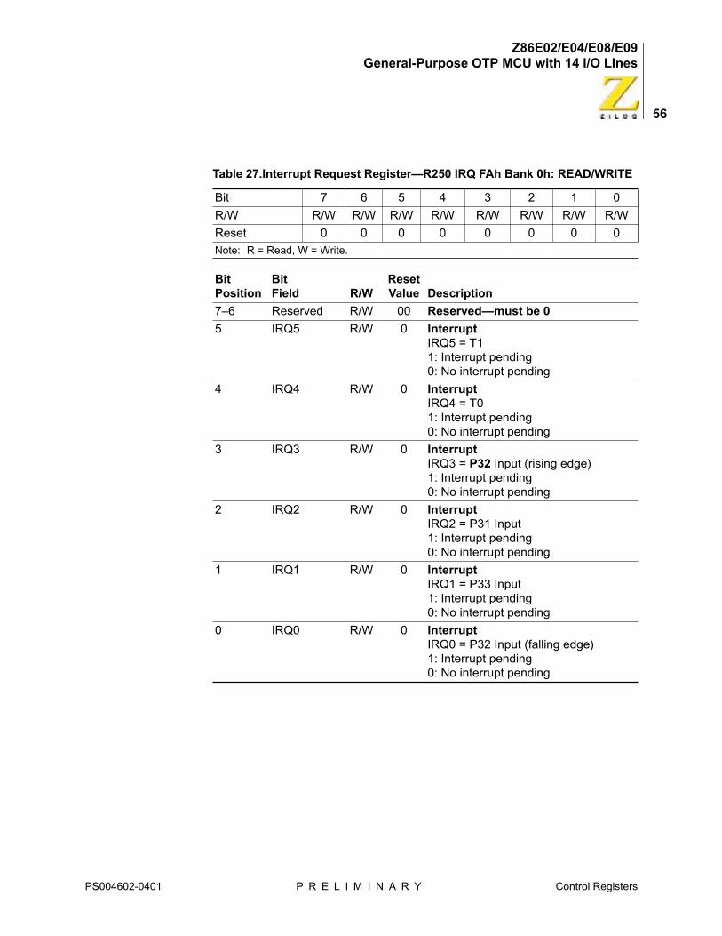
Z86E02/E04/E08/E09General-Purpose OTP MCU with 14 I/O LInes
56
Table 27.Interrupt Request Register—R250 IRQ FAh Bank 0h: READ/WRITE
Bit 7 6 5 4 3 2 1 0
R/W R/W R/W R/W R/W R/W R/W R/W R/W
Reset 0 0 0 0 0 0 0 0
Note: R = Read, W = Write.
Bit Position
Bit Field R/W
Reset Value Description
7–6 Reserved R/W 00 Reserved—must be 0
5 IRQ5 R/W 0 InterruptIRQ5 = T11: Interrupt pending0: No interrupt pending
4 IRQ4 R/W 0 InterruptIRQ4 = T01: Interrupt pending0: No interrupt pending
3 IRQ3 R/W 0 InterruptIRQ3 = P32 Input (rising edge)1: Interrupt pending0: No interrupt pending
2 IRQ2 R/W 0 InterruptIRQ2 = P31 Input1: Interrupt pending0: No interrupt pending
1 IRQ1 R/W 0 InterruptIRQ1 = P33 Input1: Interrupt pending0: No interrupt pending
0 IRQ0 R/W 0 InterruptIRQ0 = P32 Input (falling edge)1: Interrupt pending0: No interrupt pending
PS004602-0401 P R E L I M I N A R Y Control Registers
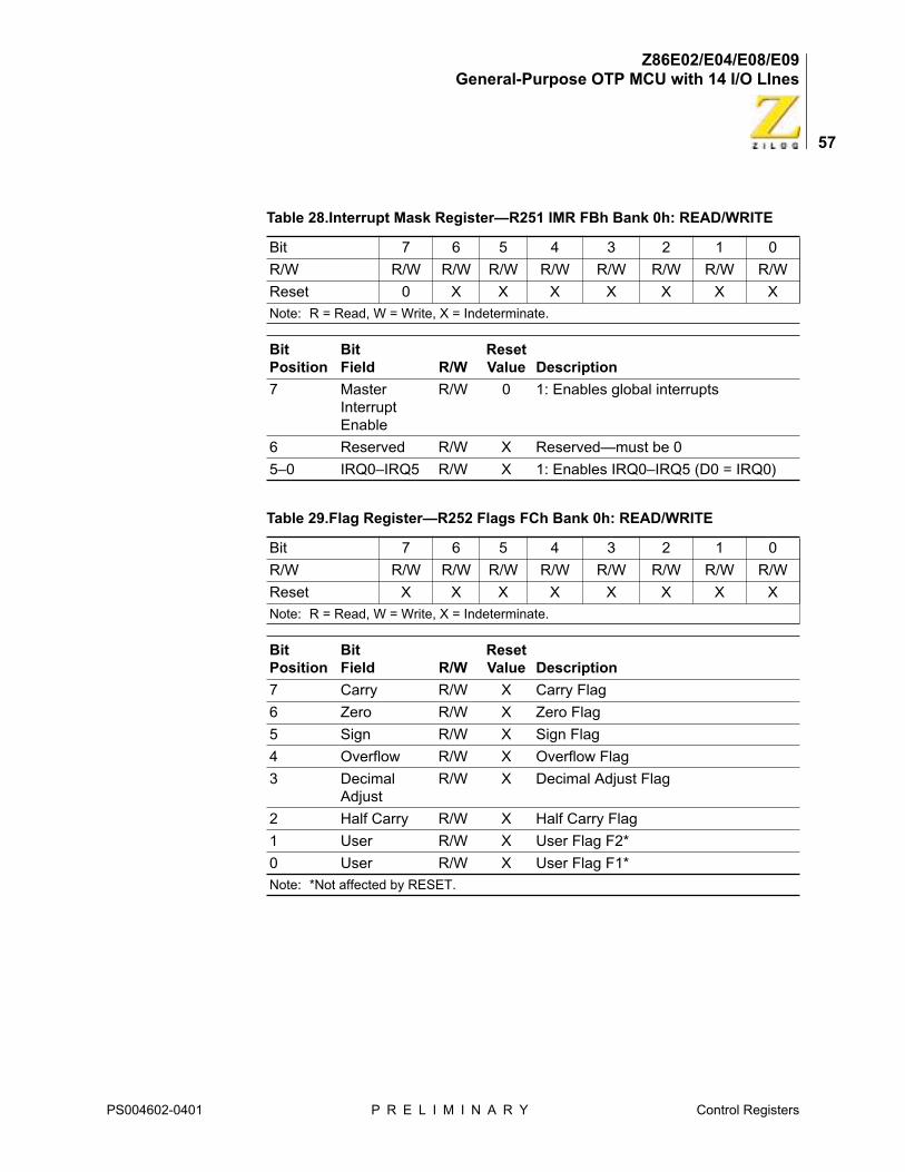
Z86E02/E04/E08/E09General-Purpose OTP MCU with 14 I/O LInes
57
Table 28.Interrupt Mask Register—R251 IMR FBh Bank 0h: READ/WRITE
Bit 7 6 5 4 3 2 1 0
R/W R/W R/W R/W R/W R/W R/W R/W R/W
Reset 0 X X X X X X X
Note: R = Read, W = Write, X = Indeterminate.
Bit Position
Bit Field R/W
Reset Value Description
7 Master Interrupt Enable
R/W 0 1: Enables global interrupts
6 Reserved R/W X Reserved—must be 0
5–0 IRQ0–IRQ5 R/W X 1: Enables IRQ0–IRQ5 (D0 = IRQ0)
Table 29.Flag Register—R252 Flags FCh Bank 0h: READ/WRITE
Bit 7 6 5 4 3 2 1 0
R/W R/W R/W R/W R/W R/W R/W R/W R/W
Reset X X X X X X X X
Note: R = Read, W = Write, X = Indeterminate.
Bit Position
Bit Field R/W
Reset Value Description
7 Carry R/W X Carry Flag
6 Zero R/W X Zero Flag
5 Sign R/W X Sign Flag
4 Overflow R/W X Overflow Flag
3 Decimal Adjust
R/W X Decimal Adjust Flag
2 Half Carry R/W X Half Carry Flag
1 User R/W X User Flag F2*
0 User R/W X User Flag F1*
Note: *Not affected by RESET.
PS004602-0401 P R E L I M I N A R Y Control Registers
Z86E02/E04/E08/E09General-Purpose OTP MCU with 14 I/O LInes
58
Table 30.Register Pointer—R253 RP FDh Bank 0h: READ/WRITE
Bit 7 6 5 4 3 2 1 0
R/W R/W R/W R/W R/W R/W R/W R/W R/W
Reset 0 0 0 0 0 0 0 0
Note: R = Read, W = Write.
Bit Position
Bit Field R/W
Reset Value Description
7–4 Working Register Pointer
R/W 0 Working Register Pointer
3–0 Reserved R/W 0 Must be 0
Table 31.General Purpose Register—R254 GPR FEh Bank 0h: READ/WRITE
Bit 7 6 5 4 3 2 1 0
R/W R/W R/W R/W R/W R/W R/W R/W R/W
Reset 0 0 0 0 0 0 0 0
Note: R = Read, W = Write.
Bit Position
Bit Field R/W
Reset Value Description
7–0 Stack R/W 0 General Purpose Register
Table 32.Stack Pointer Low—R255 SPL FFh Bank 0h: READ/WRITE
Bit 7 6 5 4 3 2 1 0
R/W R/W R/W R/W R/W R/W R/W R/W R/W
Reset 0 0 0 0 0 0 0 0
Note: R = Read, W = Write.
Bit Position
Bit Field R/W
Reset Value Description
7–0 Stack R/W 0 Stack Pointer Lower Byte (SP0–SP7)
PS004602-0401 P R E L I M I N A R Y Control Registers
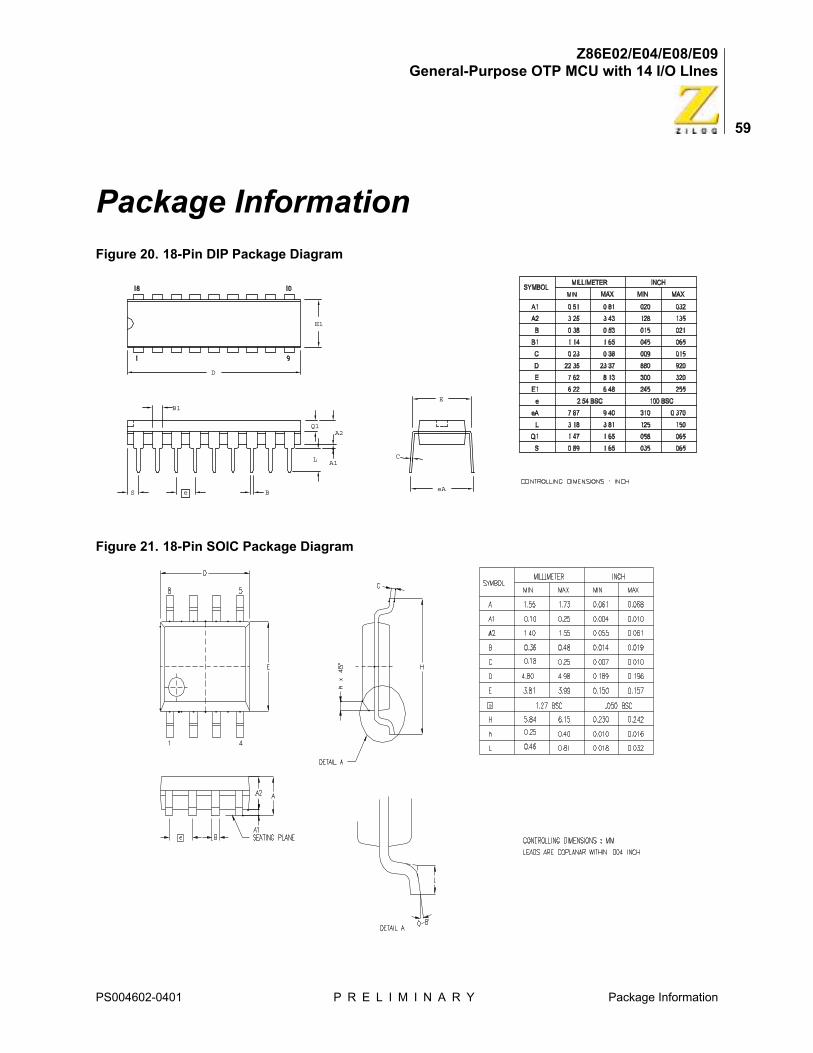
Z86E02/E04/E08/E09General-Purpose OTP MCU with 14 I/O LInes
59
Package Information
Figure 20. 18-Pin DIP Package Diagram
Figure 21. 18-Pin SOIC Package Diagram
eA
E
C
A2
A1
Q1
S e
L
B
D
B1
E1
PS004602-0401 P R E L I M I N A R Y Package Information
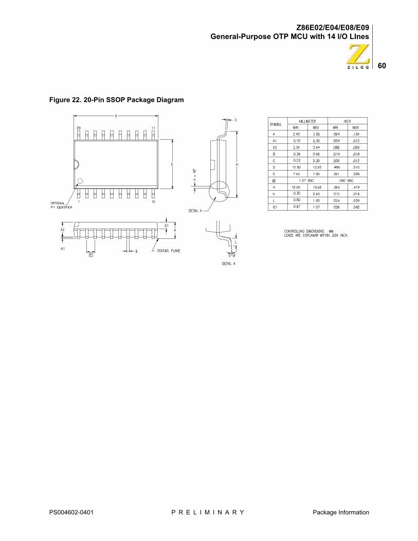
Z86E02/E04/E08/E09General-Purpose OTP MCU with 14 I/O LInes
60
Figure 22. 20-Pin SSOP Package Diagram
PS004602-0401 P R E L I M I N A R Y Package Information
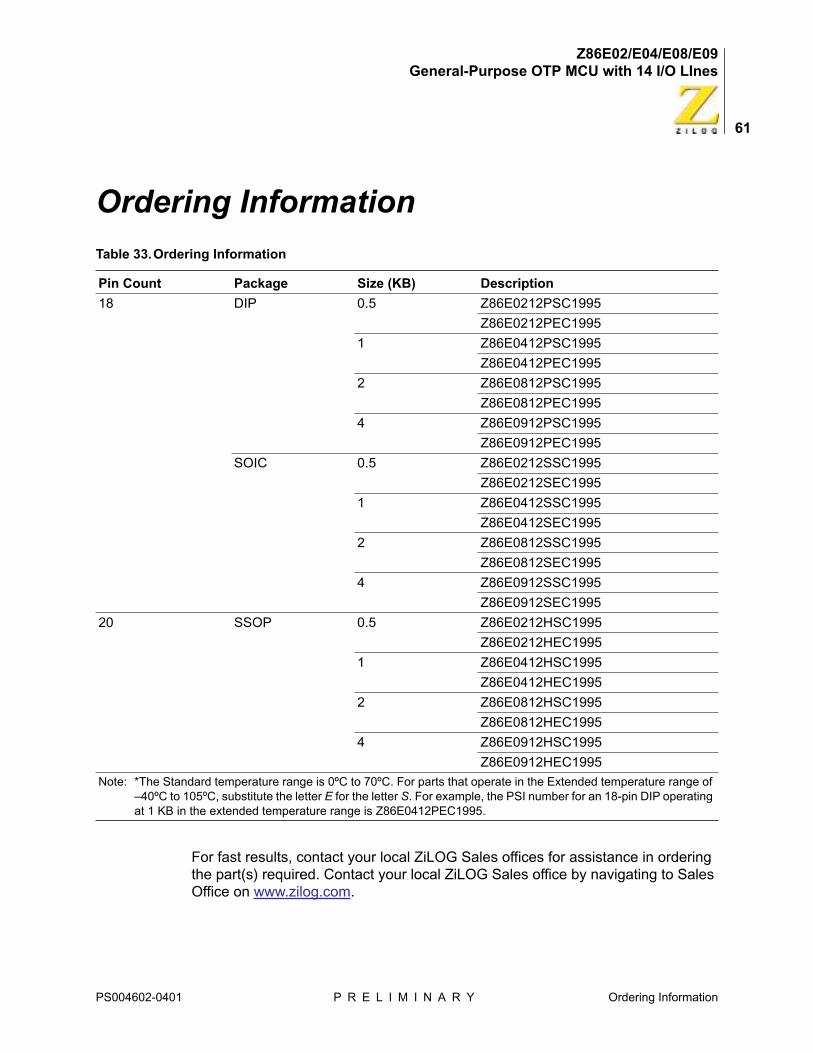
Z86E02/E04/E08/E09General-Purpose OTP MCU with 14 I/O LInes
61
Ordering Information
For fast results, contact your local ZiLOG Sales offices for assistance in ordering the part(s) required. Contact your local ZiLOG Sales office by navigating to Sales Office on www.zilog.com.
Table 33.Ordering Information
Pin Count Package Size (KB) Description
18 DIP 0.5 Z86E0212PSC1995
Z86E0212PEC1995
1 Z86E0412PSC1995
Z86E0412PEC1995
2 Z86E0812PSC1995
Z86E0812PEC1995
4 Z86E0912PSC1995
Z86E0912PEC1995
SOIC 0.5 Z86E0212SSC1995
Z86E0212SEC1995
1 Z86E0412SSC1995
Z86E0412SEC1995
2 Z86E0812SSC1995
Z86E0812SEC1995
4 Z86E0912SSC1995
Z86E0912SEC1995
20 SSOP 0.5 Z86E0212HSC1995
Z86E0212HEC1995
1 Z86E0412HSC1995
Z86E0412HEC1995
2 Z86E0812HSC1995
Z86E0812HEC1995
4 Z86E0912HSC1995
Z86E0912HEC1995
Note: *The Standard temperature range is 0ºC to 70ºC. For parts that operate in the Extended temperature range of –40ºC to 105ºC, substitute the letter E for the letter S. For example, the PSI number for an 18-pin DIP operating at 1 KB in the extended temperature range is Z86E0412PEC1995.
PS004602-0401 P R E L I M I N A R Y Ordering Information
Z86E02/E04/E08/E09General-Purpose OTP MCU with 14 I/O LInes
62
Part Number Description
ZiLOG part numbers consist of a number of components. For example, part num-ber Z86E0412PSC1995 is a 12-MHz 18-pin DIP that operates in the –0ºC to +70ºC temperature range, with Plastic Standard Flow. The Z86E0412PSC1995 part number corresponds to the code segments indicated in the following table.
Z70 .35Tµ Process
The Z86E02/E04/E08/E09 family of parts are manufactured using ZiLOG’s new advanced Z70 .35Tµ process. This process no longer requires the conventional 12.5VDC programming voltage—it operates with only 5VDC. Please refer to the Programming Specification for further information. Special consideration must be made in existing designs with this new process. Please contact the ZiLOG World Wide Customer Support Center for further information.
Precharacterization Product
The products represented by this document are newly introduced; hence ZiLOG has not completed a full characterization of the product. This document states what ZiLOG knows about this product at this time; however, additional features or nonconformance with some aspects of this document may be found, either by ZiLOG or its customers, in the course of further application and characterization work. In addition, ZiLOG cautions that delivery may be uncertain at times, due to start-up yield issues.
ZiLOG, Inc.910 East Hamilton Avenue, Suite 110Campbell, CA 95008Telephone (408) 558-8500FAX 408 558-8300Internet: www.zilog.com
Z ZiLOG Prefix
86 Z8 Product
E OTP Product
04 Product Number
12 Speed (MHz)
P Dual In-line Processor
S Standard Temperature
C Environmental Flow
PS004602-0401 P R E L I M I N A R Y Ordering Information
Z86E02/E04/E08/E09General-Purpose OTP MCU with 14 I/O LInes
PS004602-0401 P R E L I M I N A R Y Document Information
63
Document Information
Document Number Description
The Document Control Number that appears in the footer of each page of this document contains unique identifying attributes, as indicated in the following table:
Change Log
PS Product Specification
0046 Unique Document Number
02 Revision Number
0401 Month and Year Published
Rev Date Purpose By
01 03/01 Original issue K. Low, R. Beebe
02 04/01 Revise DC voltage specs K. Low, R. Beebe
Z86E02/E04/E08/E09General-Purpose OTP MCU with 14 I/O LInes
PS004602-0401 P R E L I M I N A R Y Index
64
Index
A–ECarry Flag 57Change Log 63Counter/Timer 0 53Counter/Timer 1 52Customer Feedback Form 63Customer Information 63Decimal Adjust Flag 57Document Information 63Document Number Description 63External Timing Input 52
H–OHalf Carry Flag 57Interrupt Group Priority 55IRQ0 55–56IRQ1 55–56IRQ2 55–56IRQ3 55–56IRQ4 55–56IRQ5 55–56Master Interrupt Enable 57Overflow Flag 57
P–ZP3M 54Part Number Description 62Plastic Standard Flow 62Port 2 Mode Register 53Port 3 Mode Register 54Precharacterization Product 62Prescaler 0 Register 53Prescaler 1 Register 52Prescaler Modulo 52–53Problem Description or Suggestion 63Product Information 63Return Information 63Sign Flag 57T0 Count 51T1 Count 51TIN 51–52TIN Mode 51Trigger Input 51User Flags 57Working Register Pointer 58Zero Flag 57
Z86E02/E04/E08/E09General-Purpose OTP MCU with 14 I/O LInes
PS004602-0401 P R E L I M I N A R Y Customer Feedback Form
65
Customer Feedback FormZ86E02/E04/E08/E09 Product Specification
If you experience any problems while operating this product, or if you note any inaccuracies while reading this Product Specification, please copy and complete this form, then mail or fax it to ZiLOG (see Return Information, below). We also welcome your suggestions!
Customer Information
Product Information
Return Information
ZiLOGSystem Test/Customer Support910 E. Hamilton Avenue, Suite 110, MS 4–3Campbell, CA 95008Fax: (408) 558-8536Email: [email protected]
Problem Description or Suggestion
Please provide a complete description of the problem or suggestion. If you are reporting a specific problem, include all steps leading up to the occurrence of the problem. Attach additional pages as necessary._______________________________________________________________________________
_______________________________________________________________________________
_______________________________________________________________________________
_______________________________________________________________________________
_______________________________________________________________________________
_______________________________________________________________________________
Name Country
Company Phone
Address Fax
City/State/Zip E-Mail
Serial # or Board Fab #/Rev. #
Software Version
Document Number
Host Computer Description/Type