general disclaimer one or more of the following statements ...samples and some information...
TRANSCRIPT

General Disclaimer
One or more of the Following Statements may affect this Document
This document has been reproduced from the best copy furnished by the
organizational source. It is being released in the interest of making available as
much information as possible.
This document may contain data, which exceeds the sheet parameters. It was
furnished in this condition by the organizational source and is the best copy
available.
This document may contain tone-on-tone or color graphs, charts and/or pictures,
which have been reproduced in black and white.
This document is paginated as submitted by the original source.
Portions of this document are not fully legible due to the historical nature of some
of the material. However, it is the best reproduction available from the original
submission.
Produced by the NASA Center for Aerospace Information (CASI)
https://ntrs.nasa.gov/search.jsp?R=19710028328 2020-05-06T05:30:54+00:00Z
Contract No. NAS6-256671,
September 15, 1971 19711%
FI14AL REPORT
PROJECT NO. A--1240
CK —0100
DEVELOPMENT OF MICROCIRCUITS
FOR SPACE APPLICATIONS
_ nn
By L. N. Tharp
^vOct
1911 r
`" R^^fIVFr•v
Prepared for ? XN "1 S7i `) ~ar
NASA Marshall Space Flight Center 19.5 b ^^,
ilk
Engineering Experiment Station
GEORGIA INSTITUTE OF TECHNOLOGYAtlanta, Georgia
ry fY 7L_- 310 (ACCESSiOr MBER)
a _
O (PAGES)
d (NASA X OR MX OR AD NUMBLR)
(THkU)
(C
(CATEGORY)
1 T4 !
ENGINEERING EXPERIMENT STATIONof the Georgia Institute of Technology
Atlanta, Georgia
DEVELOPMENT OF MICROCIRCUITS
FOR SPACE APPLICATIONS
by
L. N. Tharp
September 15, 1971
1
Contract No. NAS8-2566'NASA Marshall Space Flight CenterGeorgia Tech Project No. A-1240
f
m..samsLln^z 9orr"y" .. ye+e_,mssiae':i _n .«_ .-. _ z'..'r. ... --^.^. .e ElT^fi "''':':—ya

TABLE OF CONTENTS
t
Section Page
I. INTRODUCTION . . . . . . . . . . . . . . . . . . . . . . 1
II. EXPERIMENTAL SYSTEM AND TECHNIQUES . . . . . . . . 2
III. APPLICABILITY OF AUGER SPECTROSCOPYTO SEMICONDUCTOR PROCESSING . . . . . . . . . . . . . 6
IV. EXTENDED EVALUATION OF SELECTEDPROCEGr► STEPS . . . . . . . . . . . . . . . . . . . . . 22
A. After First Oxidation . . . . . „ . . . . . . . . . . . . 22
B. After Photoresist Removal . . . . . . . . . . . . . . 24
C. After Base Boron Diffusion . . . . . . . . . . . . . . . 24
D. After Emitter Diffusion . . . . . . . . . . . . . 34
E. After Metalizat.on . . . . . . . . . . . . . . . . . . . 38
F. Completed Devices . . . . . . . . . . . . . . . . . . 41
V. CONCLUSIONS AND RECOMMENDATIONS . . . . . . . . . . 45
REFERENCES . . . . . . . . . . . . . . . . . . . . . . 48
I. INTRODUCTION
The work described herein was , performed under Contract No. NAS8-25667
with the NASA Marshall Space Flight Center. The purpose of this program was
(1) to investigate the application of Auger electron spectroscopy as an analytical
method for detecting impurities introduced during processing of semiconductor
devices and (2) to explore the correlation between surface contamination and}
selected device parameters in silicon devices. i
The program consisted of examining a number of silicon wafers selected}
from various stages of device processing with Auger spectroscopy and correlat-
ing these data with known factors in the device manufacturing process as well as
P electrical measurements of device performance after several key process steps.
at:
These sample wafers were provided by a major manufacturer of silicon power
transistors while measurements were carried out in the laboratories of the
A
Physical Sciences Division at Georgia Tech..
The results obtained in this study are discussed in the remainder of this
report. Section II briefly describes the techniques and systems utilized in this
study. Section III presents a summary of the first phase of the investigation
which was aimed at applying Auger spectroscopy to typical process steps to
determine difficulties in analysis to be encountered; the following section pre-
cents in more detail the data obtained from 50 samples examined at process
steps as indicated. Finally, in Section V, conclusions and recommendations
are discussed.
vv

II, EXPERIMENTAL SYSTEM AND TECHNIQUES
The experimental system used in these studies consisted of a large bell-jar
type ultra-high vacuum system equipped with a sphe I -al retarding field electron
energy analyzer for generating the Auger spectra and a special multiple sample
turret assembly for sequentially analyzing five wafer type samples.
The vacuum chamber was evacuated by a combination of a Welch 270 l/s
Turbo Molecular pwnp and a Varian 450 1/s noble gas Vac Ion pump with auxiliary
titanium sublimation. This system combined the features of fast pumping from at-
mospheric pressure for rapid cycling and the clean, low ultimate pressure associ-
ated with ion pumped systems. Typically, following the introduction of five sam-
, ples, the system is roughed out mechanically until the Turbo pump can be started.
The Turbo pump quickly reduces the system pressure to the 10-7 Torr range at
which point the Turbo pump is valved off from the system and the Ion pump valved
in. This causes a further rapid reduction in system pressure with total pump-
down time from atmosphere to the 10 -9 Torr range of less than three hours.
System-ultimate with no baking is 1 x 10 -10 Torr. Both ultimate pressure and
pumpdown time are improved considerably with occasional mild baking of the sys-
tem, but such was not warranted for most measurements. This system is shown
in Figure 1.
To facilitate the rapid analysis of a number of samples, it was necessary
to design a special sample holder which is shown in Figure 2. This holder pro-
vides for handling five wafer type samples ranging in diameter from 1 to 1 1/4
inches. (Smaller or larger samples may also be accommodated with minor modi-
fications) . Each sample is isolated both electrically and thermally from the other

EGJy
Sryy
iUC1CL
frUU
Q;
Uf^
b0—4
44

vabv
w
wr.+
Q)
f.l
..racv
c^
cv
a^s.
6^0
G:

samples. The sample turret can be rotated so that each of the five samples can be
moved into a number of different positions providing for Auger analyais, indirect
electron bombardment heating and R,E-DC sputtering for sample cleaning. Elo^tri-r
cal contact to the samples is accomplished through a selector switch arrangement
near the center of the sample turret.
To generate the Auger spectrum for chemical analysis, the sample is bom-
barded by a beam of moderate energy primary electrons (50 microamps at 1 to 3
kev). The primary electrons ionize impurity atoms near the surface by removing
electrons from the lower lying energy levels. An empty level is filled by the
absorption of an electron from an upper level with the energy thus released appear-
ing in the form of an Auger electron ejected from a nearby upper level. The Auger
electrons are then detected in the electron energy analyzer 1. and measured values
may be compared with published tables of atomic energy levels to identify the par-
ticular :impurity. Be,---3 itivity for the technique is on the order of a hundredth of a
monolayer coverage or about 1013 atoms per cm2 ; detection depth is Limited to
several atomic layers.
The electron energy analyzer is of the spherical retarding field type.1
This analyzer consists of three concentric, spherical grids fabricated from 100
mesh gold-plated tungsten cloth woven from one mil wire. These grids have ap-
proximately 90% transmission. Electrons are collected on a spherical screen
coated with a fluorescent material which facilitates alignment of the electron
beam. The primary beams is derived from a modified Superior Electronics 3k/
5u electron gun arranged for glancing incidence.
5

k
E
111. APPLICABILITY Or AUGER SPECTROSCOPY TOSEMICONDUCTOR PROCESSING
To determine the applicability of Auger spectroscopy to the types of prob-
lems encountered in semiconductor device processing, it was decided that the
first phase of this program would consist of an examination of a relatively small
number of samples covering a number of specific process steps. The steps con-
sidered were wafer polishing, cleaning, first oxidation, base diffusion, emitter
diffusion, masking and metalization. The results of this phase have been reported
in the monthly progress letters and only selected data are presented below to indi-
cate the usefulness of the technique.
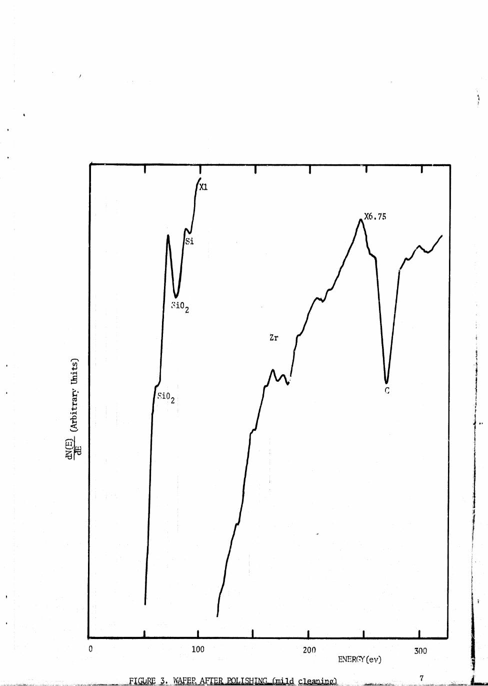
The first samples examined were silicon wafers which had been cut, pol-
ished and cleaned by the supplier. These wafers were bright and showed no opti-
cal evidence of contamination, even though the wafers had not been subjected to
the final cleaning just prior to first oxidation. An Auger spectrum obtained from
one of these wafers is shown in figure 3. The portion of the spectrum displayed
exhibits a number of peaks corresponding to silicon, silicon oxide and carbon as
labeled on the figure. Not shown is the structure at approximately 500 ev corres-
ponding to oxygen which was seen on all samples. The main feature of interest on
this sample is the structure in the spectrum lying between 100 and 200 ev. This
spectrum has been shown to correspond to zirconium.
Discussions with the manufacturer suggested that this problem of zirconium
contamination remaining on the in-coming wafers was of sufficient importance to
warrant a more detailed investigation. It was learned that these wafers were pol-
ished using a commercial preparation supplied by the Tizon Chemical Corporation
xi
xb, 75
,1ioz
Zr
.4i 2
QalSk
a
0 100 200 300E:V:RR;Yeij)
FIGURE 3. _:_ N F P. AFT,.E, ML M N (,, ^:7

and designated as Lustrox 1000. The Tizon Corporation provided us with chemical
samples and some information concerning composition. The major constituent in-
dicated is ZrO (331k) with significant impurity concentrations of Na and lif. Trace
quantities of Al, Ca, Mg, Cu Fe are also found, although no effort is made to
routinely monitor concentrations. One proprietary ingredient is also present but
was not specified,
To demonstrate that the observed impurity spectrum, derived from zircon-
ium residue left from the polishing operation comparison was made with published
spectra for zirconium and with spectra obtained from a silicon wafer intentionally
contaminated with the polishing compound in question, The wafer was coated with
small amounts of the Lustrox 1004 such that the thickness varied from heavy on
one side of the wafer to zero coating on the opposite side. Spectra, were then ob-
tained at various points along this thickness gradient and a typical curve is shown
in Figure 4.
Comparing the spectrum obtained from the intentionally contaminated wafer
with that of the wafers as received (Figure 3) confirmed the conclusion that the in-
coming wafers were contaminated with a zirconium residue in spite of the clean
optical appearance of these wafer surfaces. However, it was interesting to note
that the amount of zirconium indicated by the Auger spectrum varied from wafer
to wafer. This gives weight to the logical conclusion that the zirconium is pres-
ent as essentially isolated particles of ZrO imbedded in the surface.
The next question of importance was that of removing this particular im-
purity before first oxidation. For comparison one of the polished wafers exhibit-
ing significant zirconium contamination was removed from the Auger system and
az 8

I - IT
i
l
Zr
,w
i
}p
1'.
F
fyT
j
1.
i
r1I
^ v
^yr
i
0 100 200 300
ENERGY (ev)
FIGURE4. WAFER INTENTIONALLY CO"T^AI^^INATED WITH e,.be-4"w a^

P
cleaned. This cleaning included a dilute HF dip and subsequent mild heating in
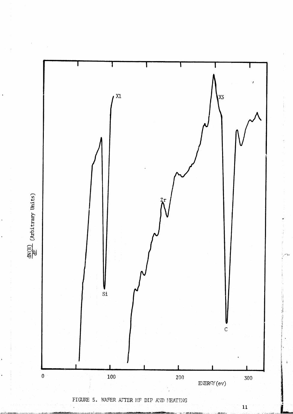
1 vacuum. The resulting spectrum is shown in Figure 5. Again comparing this curve
with that of Figure 3 0 it may be noted that the cleaning resulted iin an enhancement
of the carbon peak and a stripping of the silicon oxide as would be expected. This
stripping action is evident in the Auger spectrum from the disappearance of the sili-
con oxide peaks and the increase of the pure silicon Auger peak. On the other hand,
the Auger peaks corresponding to the zirconium were little changed and were even
increased in intensity, probably due to the removal of other superficial impurities.
To round out this question of zirconium removal, other measurwzments were
made on several wafers supplied after the final cleaning just prior to ;first oxidation.
These wafers showed considerable improvement with regard to zirconium conami-
nation, although there was evi0ence, as indicated in Figure 6, to show that the re-
moval of the impurity was not complete. This fact was substantiated in measure-
ments on samples considered in the second phase of the program and discussed in
the next section.
The next process step considered in this study was first oxidation. A typi-
cal curve for the two wafers examined is shown in Figure 7. The samples at this
particular processing step appeared to be very clean. Carbon contamination was
{
L
reduced, and, as would be expected, the pure silicon peak disappeared leaving a
large silicon oxide peak as shown in the figure. On one of these samples there
was a slight indication of impurity structure in the region around 200 ev. This
structure was tentatively identified as ruthenium, and it was suggested that the
source might be in connection with the quartz tubes used in the oxidation furnace
It must, however, be noted that the data available was insufficient for a firm con
10
H
r
xi X5
4
Zr
Si
C
F - r '4 7
r,i7
Q 100 200 300E:3ER iY (ev)
FIGURE S. WAFER krTER CIF DID' A!- .ID T 1EAr TNG
s
i
i

I S f
U
HN
ri
N
(s;tun /a-e ;Tgab)
i
t'
MyaNAG
wC7, cxM c
^
h• IIIU
o ;jCDN H
WI
^( 4
A
II
Q
Ln
7
Q^
F^yJ
L.JNNr
1
C
Int

I
OLn
aa
„11
r s
HQ^A
DU
^ H^ wa
t`r
i s
o
1
1
i
r,
f
;
l
c^
U
x^
C ^N
u.
(S;Tun Xa-Ba;TgaV)(a)hTP

elusion to be drawn.
Figure 3 shows a curve obtained after final base diffusion. There is little
difference between this curve and the curves obtained after the first oxidation. It
may again be noted that slight structure corresponding to the zirconium spectrum
was observed. No evidence for boron was found probably because at this point the
surface boron glass had been etched off and the bulk diffused levels were below the
detection sensitivity for the instrument.
Similar curves were obtained after final emitter diffusion. Typical of these
curves is the Auger spectrum of Figure 9. The only essential difference in this and
the previous curve is the presence of the phosphorous peak corresponding to the
layer of this impurity left on the surface after this step in the process.
The remaining samples analyzed were concerned with contact masking and the
aluminum evaporation. Figure 10 is representative of curves obtained on two sam-
ples after contact mask, aluminum evaporated on and etched off. This Auger distri-
bution brings out features similar to the earlier curves, except for the Al contribu-
tion to the peak intensity near 60 ev and, more significantly, strong impurity peaks
representing potassium and chromium. These impurities, indicated in the figure,
were not uniformly distributed on the wafer surface; some points on the wafer were
found showing little of this contamination while others were heavily contaminated.
Similar curves were obtained after contact mask, sample cleaned and ready
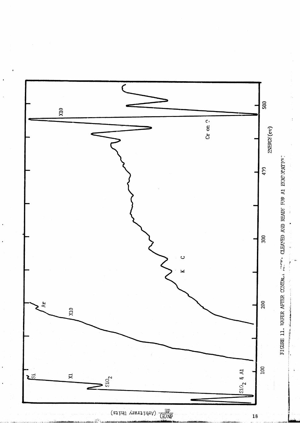
for aluminum evaporation. This situation is illustrated in Figure 11.
The final two curves show results obtained for the wafer after the aluminum
i
mask. Figure 12 shows that the spectrum is dominated with carbon and oxygen,
while Figure 13 obtained on a different spot shows heavy chromium contaimination.

I ;^
I ;
(s;Tufl Aaua4-rqaV) 15
CDC)r-i
I
Ln
P4
C)t3
uo
co
CNI

NOr4
_C^I'
i'Y
CIA a,
K
i
J
1
C^
7
1
o ^br
CHi
H ^ IA
^
♦
9
1i
W}
it
r.
CDN Hw
t
T
i^
oar-1
r _
Ta) NP 16h: s

cz
it
^HH
ip
x.
0
cD
3p(9)NP 17
(sWlEz ,z - 9P(9) NP 18
Le)
PP
ELI
rl

C)ON
Oe
a
r-{i
7
1
I
W
/L1
VM
tr
(s4Tun Aavl -4zgaV) --19{_..._ _3 La

mom
C)
low
iii
0-%
P6
ct
L4
<4
C=)
C)C:Icv
Ln
C)
(sq. Tun (-iL,.i;TqzV) 2PWIN
20

r
The sources of these impurities were not specifically identified although a localized
nature was implied.
All total, in the first phase of this study of the applicability of Auger spec-
troscopy to semiconductor processing, thirty wafers were examined for impurities
including six supplied by NASA. The results obtained and summarized in this see-
tion clearly show that there are contamination problems inherent in the types of
processing used to manufacture semiconductor devices which can be studied and
monitored using this electron scattering technique. Results of this first phase
have been discussed with the manufacturer supplying these wafers and, already
steps have been taken to upgrade the processing methods to reduce residual con-

IV. EXTENDED EVALUATION OF SELECTED PROCESS STEMS
After demonstrating that Auger Spectroscopy could be successfully applied
to contamination problems of interest in semiconductor processing, the next phase
of the program was designed to provide a more detailed examination of selected
process steps. This would more completely specify the extent of observed contam-
ination states and lay the groundwork for correlations with variations of electrical
parameters. Results obtained in examining these process steps are presented be-
low.
A. After First Oxidation
At this step ten wafers were examined as received following first oxidation.
These wafers represented two each selected from five batches. Contaminants ob-
served included zirconium, ruthenium, sulfur and a peak corresponding to either
boron or chlorine. The curve presented in Figure 14 is typical of curves obtained
on the majority of the ten wafers. For each wafer at least five Auger spectra were
obtained at different positions on the wafer surface.
The most outstanding features seen in the Auger distribution of Figure 14
are the peaks corresponding to silicon oxide and oxygen as indicated on the curve.
However, of more interest are the peaks re rTesenting ruthenium and zirconium.
These impurities were observed on all of the ten wafers examined with relatively
little variation in amounts of the indicated impurities. By comparison with the
major peak, found in the spectrum one would estimate the average surface cover-
age to be substantially below a full monolayer. To verify the ruthenium structure
comparison: was made with published spectra for ruthenium foil. The zirconium
spectra was verified by comparison with measurements described earlier.
22u.._
i..

r -` f
w r
r
r
X20
X20
X2
k
r'1j
1
4
}
I"7
5102 C
P•uu
i
^w Zr
r.
5102
0
200 300 400 S00 600
ENERGY (ev)
WAFER AFTER FIRST OXIDATION 23
w
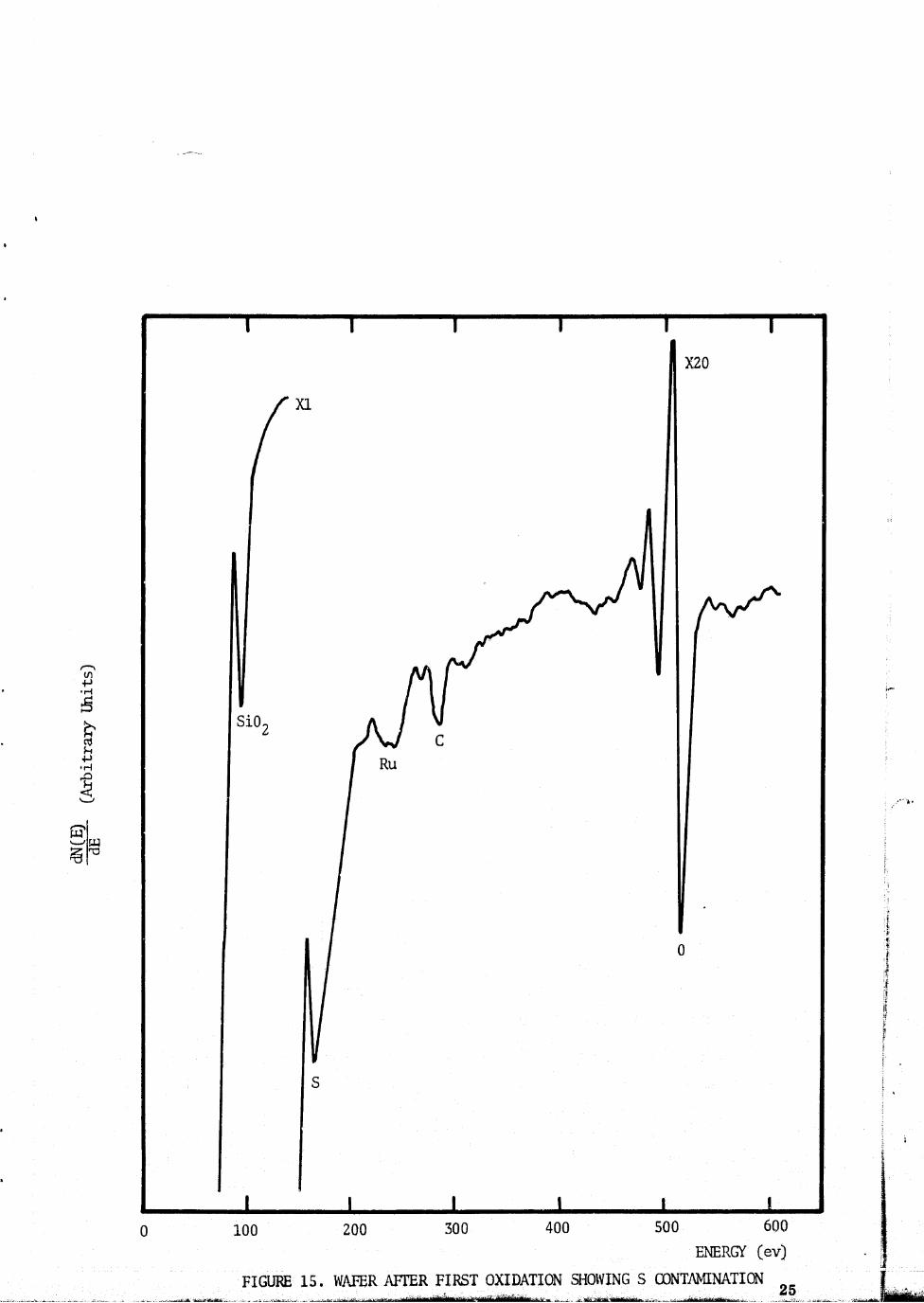
In addition to these impurities sulfur was found to be a minor impurity on
all the wafers after first oxidation, although, in this case, the amount present
varied to a greater extent. Figure 15 shows strong sulfur contamination which was
observed on two wafers. This curve also shows ruthenium structure even though
the zirconium spectrum is below detectable limits.
In the case of two wafers a strong peak was also observed at 180 ev which
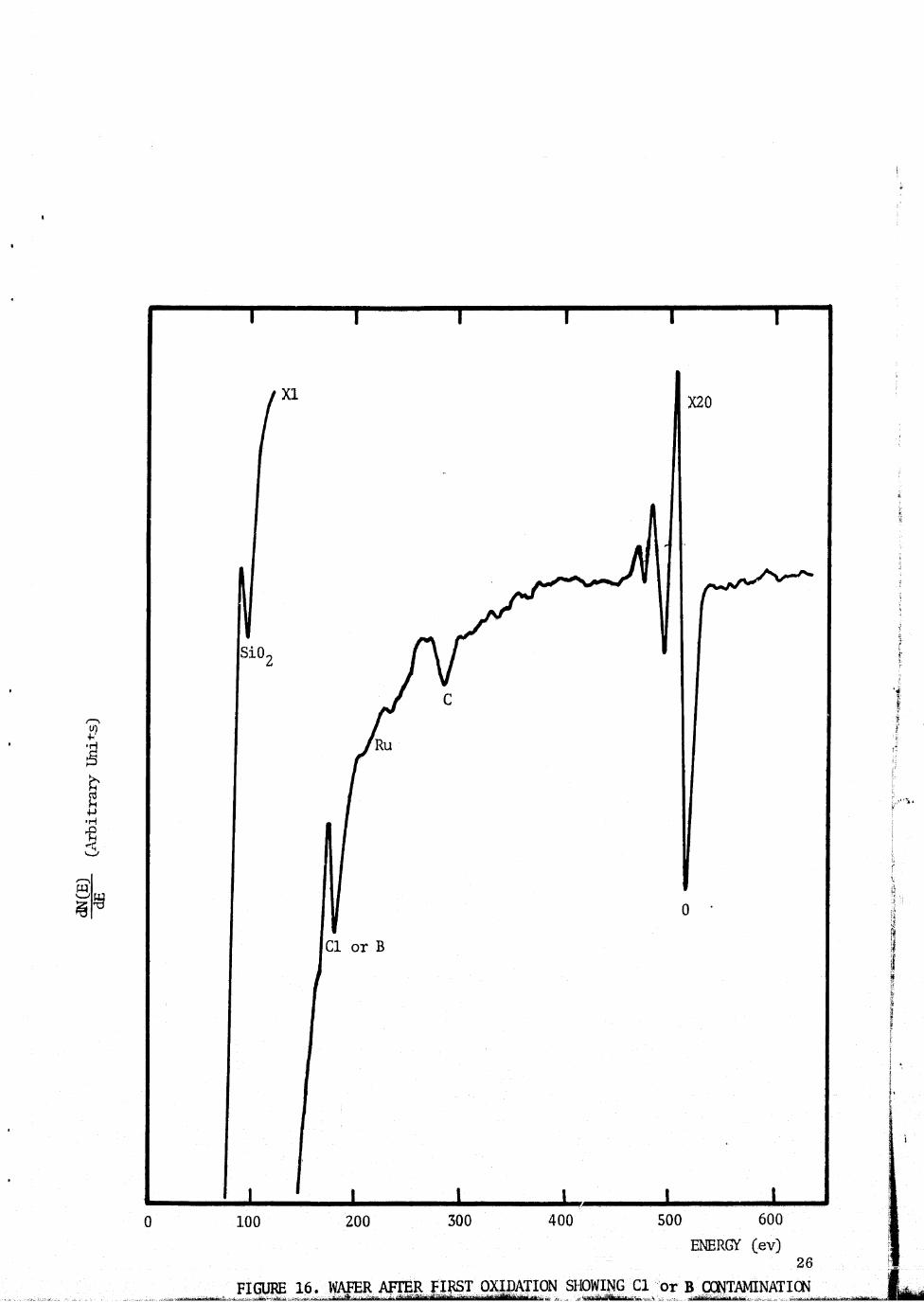
could be either boron or chlorine. This is shown in Figure 16. It must be recalled
that the Auger peak alone is not sufficient information to differentiate between the
possible contaminants of chlorine and boron. One of these wafers was one which
also exhibited greater sulfur contamination than generally found.
B. After Photoresist Removal
The second step examined in greater detail was the removal of photoresist
following base mashing, Ten wafers were examined and generally found to be
ra ther clean, as indicated in the curve of Figure 17. This curve shows the normal
silicon oxide peaks and carbon as well as minor impurity concentrations of sulfur
and silver. It was the latter impurity, silver, which proved to be of greatest in-
terest as discussed in the next section. Silver was fo .xnd in sub- , monolayer quanti-
ties on several of the ten wafers.
This particular process step was difficult to characterize with Auger data
because of surface charging.. This charging resulted in peak splitting for some of
the Auger curves obtained--its cause was not determined, In spite of this problem,
some good data was obtained on each of the t,-;n wafers
C. After Luse Boron Diffusion
Again at this step ten wafers were examined and electrical measurements
Yi
24
X20
Xi
Si02C
Ru
w^ro
0
S
0 100 200 300 400 S00 600
ENERGY (ev) a
FIGURE 15. WAFER AFTER FIRST OXIDATION SHOWINGS CONTAMINATION 25
X1
Si02
U)
0 100
FIGURE'
w
r 'b T
I
i

9r
!v1
T
4JIr4
v
WU
r,_ .
- --I ^W-
t
X1X10
X10
ii
a1
i
3
T
S
^i
C ,a
i02
{
0
0 100 200 300 400 S00 600
iENERGY (ev)
FIGURE 17. TYPICAL WAFER AFTER BASE MWK, PHOTORESIST REMOVFD 27w^

i^
were added to the Auger spectra in an effort to establish a correlation between
sui-,ace impurities and collector-base diode leakage. Interestingly, these wafers
were among the cleanest of all wafers examined. However, minor impurities were
observed including carbon, ruthenium, and another impurity of particular interest,
silver,
The Auger spectrum of Figure 18 is typical of the majority of the spectra
obtained after base diffusion. This curve shows large silicon oxide and oxygen
peaks as expected and a moderate sized carbon peak which is not especially signi-
ficant compared with other samples characterized. Of note is the fact that the
boron peak is very small even when large amounts of surface boron might be ex-
pected; a plausible explanation for this observation is surface masking.
On one wafer the surface boron was slightly enhanced as may be seen in
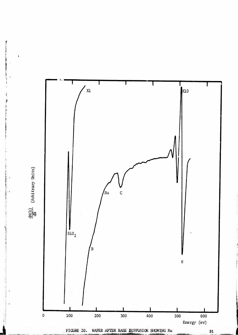
Figure 19. Ruthenium was observable though not significant on five out of the ten
wafers. This is illustrated in Figure 20.
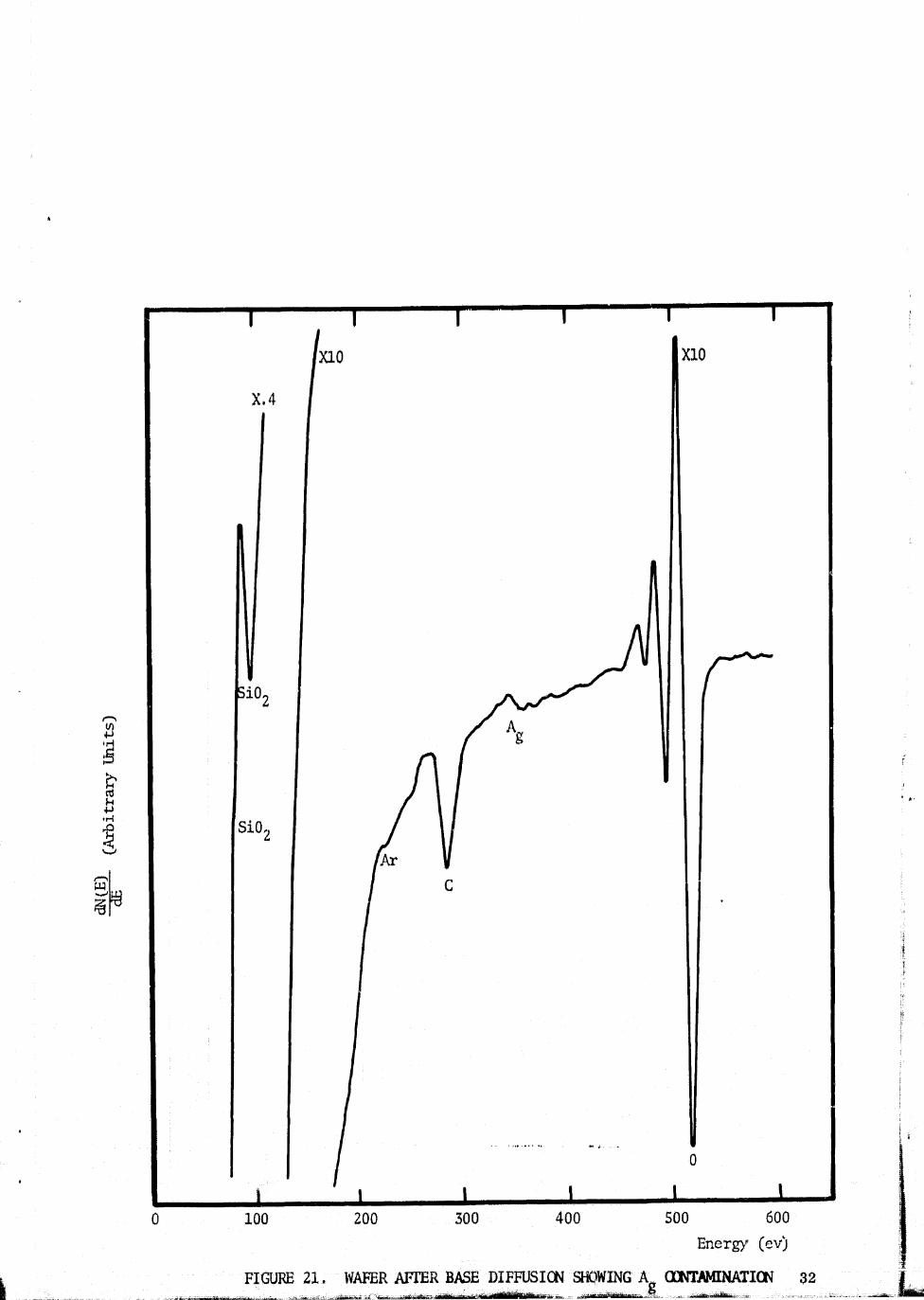
The impurity of greatest interest is that identified as silver and shown in
Figure 21. This impurity was observed in fractional monolayer quantities on sev-
eral wafers and is of interest because the wafers exhibiting this impurity seemed
to have the lowest values of diode leakage.
To establish this correlation, diode leakage currents were measured for a
numhej of diodes on each of the ten wafers. These current measurements were
made in subdued lighting with ten volts applied reverse bias Average leakage was
approximately 0. 35 microamps although some diodes showed leakage currents as
high as 1.9 p A and others as low as 0.03 p A. Generally the values of diode leak-
age measured were reasonably consistent over any particular wafer. The wafers
i
28

I
r-,w
E
.4 X10 X10
SiO2
Sio2
Ar
C
B
0
0 100 200 300 400 500 600
Energy (ev)
I ^. FIGURE 18. TYPICAL WAFER AFTER BASE DIFFUSION

e-IN
U)4-J
t^
♦ re{
r1
I
T
X:10X10
c
Sio 2
B
0
A2
0 100 200 300 400 S00 600
Energy (ev)
.FIGURE 19. WAFER AFMR BASE DIFFUSION 511OWING SURFACE BORON 30
x'
i
f
I ,
i
-11 IV,
Z:Sl
rYy
I
fi
is
is
Xi 0
Ru c
sio2
B
0
0 100 200 300 400 Soo 600
Energy (ev)
20. WAFER AFTER BASE DIFFUSION SHOWING . Ru 31
r -a am
A
xio X10
A • 4
io
g
rr-{
SiO2
Ar
C
x
0
V LVV 4,VV _ JVV 'TVV 3 VV vvv
Energy (ev)
FIGURE 21. WAFER AT-TER BASE DIFFUSION SHOWING A OONTAMINATION 32

measured fall generally into two classes with diode leakages above and below
approximately 0. 25 pA , Comparisons were made within batches simultaneously
loaded into the five sample turret for sequential Auger analysis,
In the first five sample batch average values of diode leakage were found to
be 0.1.9, 0. 13, 0.28, 0.24 and 0.1.3 microamps for the five wafers respectively.
Comparing these figures with the Auger data it was observed that both of the wafers
with the lowest leakage values exhibited surface contamination of silver. However,
the intensity of the silver peak for one of these wafers was somewhat smaller than
shown in Figure 21. No silver was seen in curves obtained for the other three sam-
ples in this batch.
Four of the five samples in the second batch had average leakage values of
0. 60, 0.28, 0.79 and 0.67 microamps. The fifth wafer was inadvertently damaged
in handling and so data obtained on this wafer are not included. It may be noted that
the lowest value of average leakage for this batch is higher than measured for the
first bateks. However, there is still a significant difference between the value of
t
^j 0.28 pA and the other values measured. In examining the corresponding Auger data,
it was again found that the vaafer with the dower leakage exhibited significant surface
contamination of silver. No silver was observed on the other three wafers,
The source of silver- contamination or its role in affecting the diode leakage
currents at this stage of device fabrication are at this point unclear. It appears that
the silver may be a residue associated with the photoresist operation or its removal.
The mechanism involved in the affect on the values of leakage would require more
E, , extensive investigation to obtain a clearer understanding of this problem.
33

r -1 ;W
D. After Emitter Diffusion
The ten wafers examined after emitter diffusion exhibited a broader range
of low-level contamination, than previously observed at other steps. Contaminants
included phosphorous, carbon, ruthenium, silver, calcium and oxygen. As for the
previous step electrical measurements were made along with Auger spectra deter-
minations in an effort to establish a correlation between break-down voltages and
surface contamination.
An Auger curve typical of the wafers after emitter diffusion is shown in
Figure 22. This spectrum shows, in addition to carbon, oxygen and silicon oxide,
minor contamination of phosphorous and nitrogen. It was further observed that the
level of carbon contamination varied significantly from point to point on the same
wafer and from wafer to wafes:, Furthermore, four of the ten wafers exhibited ruth-
enium as indicated in the Auger curve of Figure 23. Significantly three wafers also
gave evidence of silver as a surface impurity as is also shown in Figure 23. Sev-
eral wafers were found to be contaminated with very minor amounts of calcium.
This is shown in Figure 24 for one wafer which also had silver contamination as in-
dicated in the figure.
To check for a correlation with electrical parameters, measurements of
t BVCBO Were carried out for a number of devices on each wafer. These measure-
ments were made using a Tektronix transistor curve tracer. Break-down voltages
were typically found to lie in the range of 180 to 230 volts. It was of interest to notet
that the break-down voltages were not stable in time but tended to change by approx-
imately 10 per cent over a period of several minutes., The behavior of most of the
transistors checked was such that the break-down voltages initially decreased by a
34 {{

X1 X10
0
N
P
Sio C
t ,
V)4J
cd
v
w
r
i
0 100 200 300 400 S00 600
ENERGY (ev)
FIGURE 22. TYPICAL 1dAFEP. AFTER EtiiITT'ER DIFFliSION
x_ ^35.^LL_

X1x10 x10
Ag
C
Sio 2
L 0
0 100 200 300 4,00 Soo 600
PM.,','RGY (ev)
UT(--ITD'C '77 IATAUPD AFTPT? lPX4TVMP DIFFUSION SHOWING Ru AND Acy CONT, 41NATION36

/'1
V)+J
^a
.H
L 4
i
X1. /i V
X10
Si0 2Ca
C
P
0
' 0 100 200 300 400 S00 600
ENERGY (ev)
FIGURE '24 WAFER AFTER OffTTER DIFFUSION SHOWING Ca AND Ag CONTM11NATION 37
Ep
maim""

6 f
small amount and then increased to a final value approximately 20 volts greater than
the initial break-down voltages.
The devices checker' fell generally into two classes with regard to the "sharp-
ness" of the observed break-down. There was also some division of the wafers in
terms of the amount of "walk-away' observed. Six wafers showed average shifts of
break-down voltage less than 20 volts while three wafers had average shifts signifi-
cantly greater than 20 volts. One wafer was found to have very eratic break-down
voltages with time for several devices on the wafer and unusually large increases
of break-down voltage for others.
There was no correlation between the Auger data, taken after emitter diffu-
sion, and the measured collector-base breakdown characteristics. This was not
too surprising since Auger data was not available on the base diffusion for these
particular wafers, and one would expect impurities introduced during the formation
of the base-collector junction to predominate over impurities introduced at a later
step. It would be necessary to characterize a base diffusion and then put the wafer
back in the processing line for the emitter diffusion to obtain a definitive test for
correlation between Auger data and break-down or 11 walk-away" phenomena.
E. After Metalization
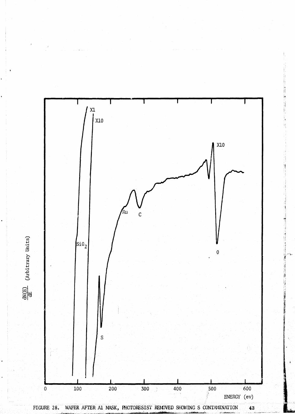
Ten wafers were examined at this stage with photoresist removed after alum-
inum masking and cleaning with wafers ready for sintering. A number of impurities
were observed including sulfur, boron or chlorine, phosphorous, carbon, oxygen
and fluorine. Typical curves are shown in Figures 25 and 26. The Auger spectra
are similar except that the carbon is seen to be reduced in Figure 26 and the fluorine
increased. One wafer showed unusual concentrations of phosphorous as indicated in
38I I
14-1

W
xi X10x10
F
Cl or B
Al
C0
S.
0 100 200 300 400
FIGURE 25. TYPICAL WRIER AFTER Al MASK, PHOTORESIST REMOVED
500 600
ENERGY (ev)
39

Y1
c^
I"7
U
r^u ^
xi 1
x10xio
sio21
r.
i
i Y S
J
SIb
C
Cl ^wT Zz is
k
0
i
b
f
J
ai
0 100 200 300 400 500 600
ENERGY ^ev^
FIGURE 26. WAFER fiFFER Al. MNSK, P140TORESIST E lOVEU SHOWING F CONTAMINATION 4 0
I - _«
_ _
Figure 27 and, while all wafers had some sulfur contamination, this contamination
was on one wafer found to be excessive as presented in the Auger spectrum of
Figure 28.
.Again because of the lack of acceptable sputtering capability it was not pos-
sible to expose underlying layers for examination for the purpose of correlating
with known electronic parameter variations.
F. Completed Devices
The final step examined in the fabrication process was the completed device.
Several transistors were mounted on a molybdenum plate for analysis, and a typical
Auger spectrum is presented in Figure 29. These devices, which were supplied
before bonding of leads, exhibited contamination similar to that reported after metal-
ization. This included impurity concentrations of phosphorous, sulfur, carbon,
nitrogen and oxygen. The most outstanding difference was the presence of an addi-
tional impurity, calcium. This impurity was present in small quantities on one of
the transistors examined and in much larger quantities on two other devices. On
these two other units the calcium appeared to dominate the Auger spectrum indi-
cating greater than monolayer average coverage.
ICI
T
fx.
i

i'
i
i^
i
0 100 200 300 400 S00 600
ENERGY (ev)
FIGURE 27. WAFER AF-MR Al M SK, PHOTORESIST RENDVED SHOWING P CONTAMINATION^_.
I
0 100 200 300 400 500 600
ENERGY (err)
FIGURE 28. WAFER AFTER Al MASK, PHOTORESIST REMOVED SHOWING S CONTMUNATION 43

xiX10
X10
a
rp
Cl nr B 0
C
s
4.J,r4
4-Jr.4
ij
Tt
Lei
4
0 100 200 300 400 Soo 600
ENERGY (ev),
FIGURE 29. TAN FROM COMPU',TED, DEVICE 44

r P-
V. CONCLUSIONS AND RECOMMENDATIONS
During the course of this investigation it has been clearly seen that Auger
Spectroscopy has application to impurity problems inherent in the processing of
seij '`conductor devices. The data obtained have provided insight into the nature of
the impurities present at the process steps investigated, although the results ob-
tained have certainly Wen subject to limitations as regards interpretation.
The most serious deficiency in this study has been in the area of reverse
sputtering of the wafer samples to expose underlying surfaces for analysis . The
desirability of tieing able to sputter off certain layers of material for determining
interfacial impurities is obvious, because this permits a far more comprehensive
characterization of the effects of a particular processing operation. This more
complete characterization will be essential for making truly meaningful corre-
lations with variations in selected electrical parameters.
The difficulty encountered in, attempts to sputter the silicon wafers, as0
described in earlier progress letters, i s that during sputtering there is a redis-
tribution of impurities and a tendency for minute quantities of the sample holder
material, in this case molybdenum, to be deposited on the samplesurface, there-
by masking the impurities of interest. All attempts at general RF-DG sputtering
with argon were unsuccessful in this regard. -However, this proble-n, should not
occur in the case of sputtering with a focused argon beam generated by a low pres-
sure ion sources Such an ion gun has now been developed and is presently under-
going finkTi testing before being added as a permanent sputtering source on the
Auger syst^.tn.

i
t
In spite of the limitations mentioned above, the data obtained in this study
0 have proven to be quite useful in evaluating some of the process steps is which dif-
ficulty was reporter] by the manufacturer. For example, the problem of zirconium
residue from the polishing operation has been greatly reduced, because the supplier
of wafers to the manufacturer has provided an additional process step to insure bet-
ter removal of the imbedded zirconium oxide particles. It is reported that this ad-
ditional step has resulted in improved process performance.
The presence of substantial amounts of carbon at many process steps is now
being evaluated by the manufacturer in an effort to explain some of the processing
problems encountered which may be traceable to carbon in the silicon material.
Similarly, the presence of impurities reported after metalization are being consid-
ered to determine the connection with occasional irreproducible surface effects .
Correlations between electrical parameters and surface impurities have in
no way been complete because of the difficulties mentioned. However, the correla-
tion observed after base diffusion between silver contamination (which appeared a
after the photo, resist step) and diode leakage currents is of interest and suggests
need for a more comprehensive study.zc
Undoubtedly, this program has demonstrated the usefulness of surface ori-
ented analytical techniques as a means of process evaluation and improvement for
semiconduetor devices. The data obtained and summarized in this report have
identified previously unknown but suspected contaminants causing difficulty in cer-
tain process steps. Further, and perhaps most importantly, the results of this
study have provided the background data and understanding of this applicationsy J,
area which may now lead to more specific studies designed to better resolve the
46
I

problem of correlating process contaminants with meaningful electrical parameters
of finished devices.
Respectfully submitted,
L. N. TharpProject Director

I %f
REFERENCES
1. L. N. Tharp and E. J. Scheibner, J. Appl. Phys. 38, 3320 (1967),.
2. J. A. Bearden and A. F. Burr, Rev. Mod. Phys. 39, 125 (1967).
3. R. E. Weber and A. L. Johnson, 28th Conference on Physical Electronics,Minneapolis, Minn., March 19, 1968,
4. T. W. Haas, J. T. Grant and G J. Dooley, Phys, Rev, B [ 3 ) 1 (4), 1449(1970) .
^: r
hN
t
i t
;{ t
is
^ ff
'.1
t
_... _. __ _ .... ..ice...