gdt tss tvs / esd hybrid device
TRANSCRIPT

Shenzhen�Bencent�Electronics�Co.,Ltd.Address:�1�floor,�E�building,�Hongfa�science�and�Technology�Park,�No.��2035,�Song�Bai�Road,�Shiyan�street,�Baoan�District,�ShenzhenHttp:�//�www.bencent.com.cn�Tel:�+86-755-26515060
GDT�/�TSS�/�TVS�/�ESD�/�Hybrid�deviceV202007

Bencent,� founded� in� 1999,� is� a�
professional� O.V.P� components� and�
innovative� solutions� provider,� with�
products� including� GDT,� TSS,� TVS,�
ESD� and� Hybrid� devices� applied� in�
t e l e commun i ca t i o n , � s e c u r i t y , �
consumer,�medical,� automobile� and�
new� energy� industry.� Bencent� also�
provides�EMC�testing,�consulting�and�
training� services� for� our� customers�
which� make� us� the� first� choice� of�
domestic� and� international� well-
known� companies,� such� as� Huawei,�
Nokia,�Samsung,�Hikvision,Lenovo,�
Foxconn�and�Panasonic.�� ⻢鞍⼭分公司

SPD BCCSP
BN
BL
What’s��New?
OGDT
BGO6000A05-LC21.2/50-8/20μs��10KV-5KA
V ≥480VBR
Φ ��� � 18.0x7.0mm Page 7
AC�POWER
Charging�stations
AC�1A-30A��Failsafe
1.6 1.0 0.55 ��� �6x x mm Page 1IPP>4A(8/20μs�)
LOW-C �ESDO
Pin2�to�Pin1�is�TSS�Pin1to�Pin�2�is�TVS
I ≥10KA@8/20μsPP V ≥75VDRM
18.3x14.0x7.0mm���Page�73
DC�POWER
RRU
1.2/50-8/20μs��10KV-12Ω��±40time
5.5x4.0x4.0 ��� �37mm Page
AC�POWER
BL201N1.2/50-8/20μs��2KV-1KA
2.9 ��� �35x2.1x1.9mm Page
AC�POWER
41x30.5x27.2mm���Page�73 6.5x6.5x0.6 ��� �59mm Page
H=0.6mm���CSP�Package��IPP>4KV(10/700μs�)
BMG20D471K801YI ≥5KA@8/20μsPP
Low�Clamping�Voltage V ≥600VBR
20x17x9mm Page 73��� �
AC�POWER
26
Air�conditioner
BVS
BVS-SMEJ8685CA
BN362M
Adapter
AdapterRJ45-10G
BV-FE03U2AC =0.25pF@1MHzO
Adapter
AC�POWER
BSPD220C20PU =250V��I =20KA��U <1.5KVC N P
RJ45
POE�Switch
BCCSP-58C-654K
Switch
BMG
V ≥2880VBR
H<2mm� V ≥140VBR
Lightning�Protect�Zone
���LPZ0B-1
���LPZ0B-2
���LPZ0B-3
���LPZ1
���LPZ2
���
Test�Standards
���ITU-T�K20�
���ITU-T�K21
���GR1089
���ISO7637
���ISO16750
���IEC61000-4-5
���IEC61000-4-4
���IEC61000-4-2
���UL60950
Equipment�V�Ports
Ports�Circuit�Design
���AC
���DC
���RJ11
���RJ45
���Coaxial
���RS485
���Other
���
V-I�curve
V-t�curve
Datasheet
���GDT
���TSS
���TVS
���ESD
����Hybrid�Deivce
Surge�Lab
Test�Waveforms
���Surge
���EFT
���ESD
���Other
�
��� Qualification�Certifisate
Reliability�Lab
Layout�
Recommended
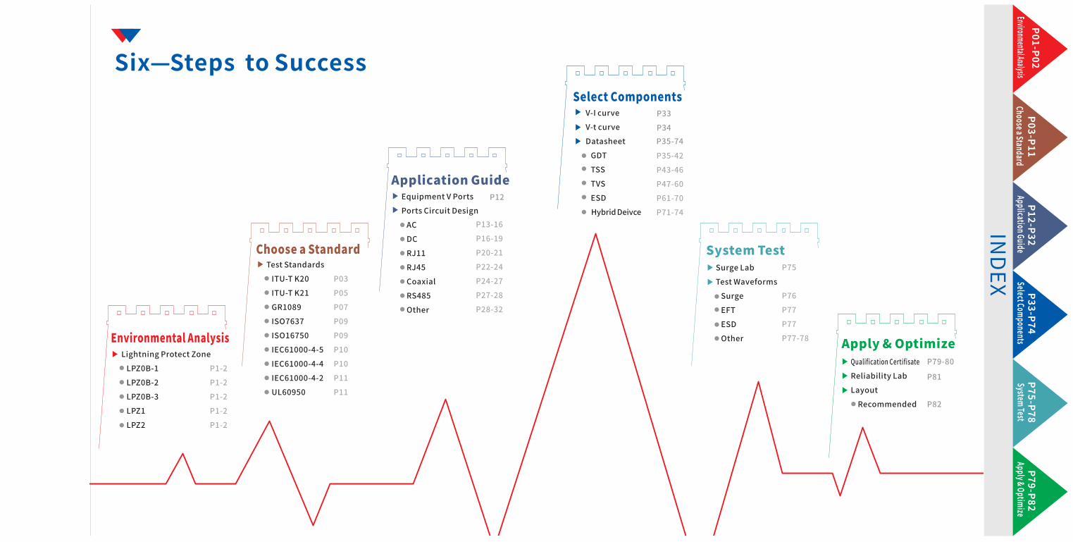
P1-2
P1-2
P1-2
P1-2
P1-2
P03
P05
P07
P09
P09
P10
P10
P11
P11
P13-16
P16-19
P20-21
P22-24
P24-27
P27-28
P28-32
P35-42
P43-46
P47-60
P61-70
P71-74
P79-80
P75
P76
P77
P77
P77-78
P33
P12
P35-74P34
P81
P82
Apply�&�Optimize
System�Test
Select�Components
Application�Guide
Choose�a�Standard
Environmental�Analysis
Six—Steps��to�SuccessIN
DEXEnvironmental�Analysis
Choose�a�StandardApplication�Guide
Select�ComponentsSystem�Test
Apply�&�OptimizeP03-P11
P12-P32P33-P74
P75-P78P79-P82
P01-P02

�HDMI
RJ45
RJ11
RS485
POWER
COAXIAL
COAXIAL
To�be�provided�with�good�line-to-ground�connection�system�and�thespecific�room�with�primary��protection,�e.g.�inside�building,generator�room�or�outdoor�container-style�mini�generator�room�etc.
Other�areas�inside�building��except�LPZ0 �classification�B
defined,�e.�g.�passageway,�weak�current�wells,�switching�room,�basement,�inside�room
LPZ1 LPZ2
RJ45RJ11 RS485POWER
RJ45RJ11 RS485POWERCOAXIAL
SPD
LPZ1
LPZ2
RRU
SPD
RS485 POWER
AISG COAXIAL
LPZ0 -1B
LPZ0 -2B
LPZ0 -3B
COAXIAL RS485 POWER RJ45 VIDEO
SPD
LPZ0 -1B LPZ0 -2B LPZ0 -3BApplication�environment�on�telecom�transmission�tower
Outdoor�cabinet�on�rooftops(high�speed�aerial�included)
General�outdoors,�walls,�hanging�bars
AISG COAXIAL RS485 DC�POWER RJ45 VIDEORJ11AC�POWER
LPZ0 -1�B
LPZ0 -2�B
LPZ0 -3�B
LPZ1�
LPZ2�
8/20μs5KA
1.2/50-8/20μs6KV-3KA�10/700μs4KV、6KV�
8/20μs5KA
1.2/50-8/20μs6KV-3KA��10/700μs4KV、6KV��1.2/50μs2KV、4KV�1.2/50μs
1KV�
8/20μs5KA�
1.2/50-8/20μs6KV-3KA��10/700μs4KV、6KV��1.2/50μs2KV、4KV�1.2/50μs
1KV�
8/20μs20KA/40KA�
8/20μs10KA/20KA�
1.2/50-8/20μs6KV-3KA��1.2/50μs2KV、4KV�1.2/50μs1KV、2KV�
8/20μs10KA/20KA��
8/20μs5KA/10KA��
1.2/50-8/20μs6KV-3KA��1.2/50μs2KV、4KV�1.2/50μs
0.5KV、1KV�
10/700μs4KV、6KV��1.2/50μs2KV、4KV�1.2/50μs
1KV�
10/700μs4KV、6KV��1.2/50μs2KV、4KV�1.2/50μs
1KV�
10/700μs4KV、6KV��1.2/50μs2KV、4KV�1.2/50μs
1KV�
Recommended�surge�level
LPZ2
Linghtning�Protect�Zone
0201
Environmental�AnalysisChoose�a�Standard
Application�GuideSelect�Components
System�TestApply�&�Optimize
Test��Stand
ards
03� 04�
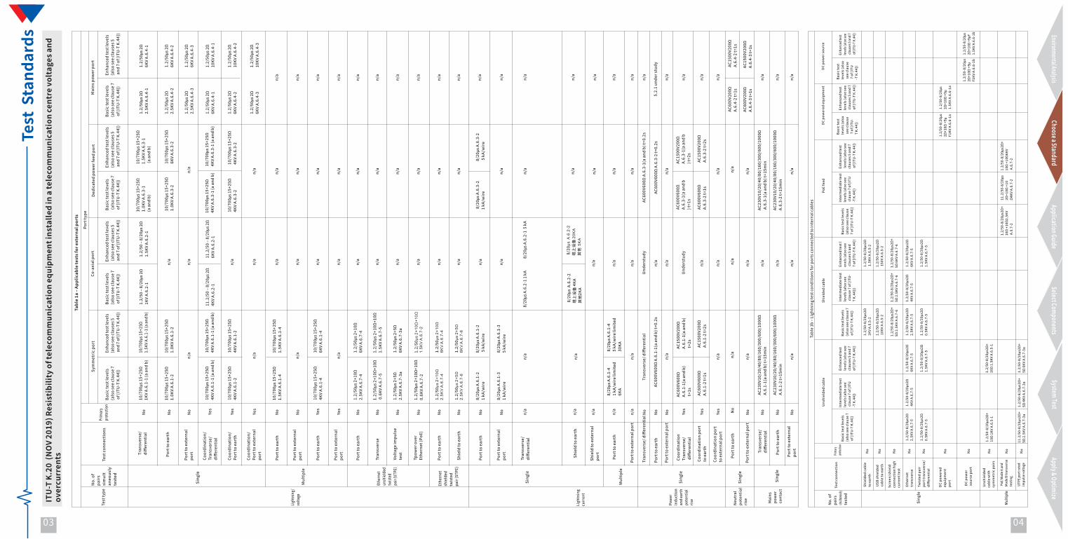
ITU-T�K.20��(N
OV�20
19)�R
esistibilit
y�of�te
leco
mmun
icat
ion�eq
uipm
ent�ins
talle
d�in�a�te
leco
mmun
icat
ion�ce
ntre
�volta
ges�a
nd�
over
curren
ts�
Environmental�AnalysisChoose�a�Standard
Application�GuideSelect�Components
System�TestApply�&�Optimize
Tabl
e�1a
�‒�App
licab
le�te
sts�f
or�exter
nal�p
orts
Test�ty
pe
Ligh
tnin
g/�
volta
ge
Ligh
tnin
g�cu
rren
t
Power
�in
duction
and�ea
rth
pote
ntial�
rise
Neu
tral�
pote
ntial
rise Mains
�po
wer
cont
act
Tabl
e�1b
�‒�Light
ning
�test�con
dition
s�for
�por
ts�con
nected
�to�in
tern
al�cab
les
No.�of�
pairs
simulta
neousl
yte
sted
Sing
le
�Mul
tiple
Test�con
nections
No.�of�
pairs�
simul
tan
eous
lyte
sted
Sing
le
Tran
sver
se/�
diffe
rent
ial
Port�to
�ear
th
Port�to
�exter
nal�
port
Coor
dina
tion
/Tr
ansv
erse
/�di
ffere
ntial
Coor
dina
tion
/Po
rt�to
�ear
th
Coor
dina
tion
/Po
rt�to
�exter
nal�
port
Port�ty
pe
Symmet
ric�po
rtCo
-axial�por
tDed
icat
ed�pow
er�fe
ed�por
tMains
�pow
er�por
t
Prim
ary�
prot
ectio
nBa
sic�te
st�le
vels�
(also�se
e�clau
se�7
�of�[IT
U-T�K.44]
)
Enha
nced
�test�le
vels�
(also�se
e�clau
ses�5
�and
�7�of�[IT
U-T�K.44]
)
10/7
00μs
�15+
25Ω
1KV�A.
6.1-
1�(a�and
�b)
No
No
No
Yes
10/7
00μs
�15+
25Ω
1.5K
V�A.
6.1-
1�(a�and
�b)
10/7
00μs
�15+
25Ω
1.0K
V�A.
6.1-
210
/700
μs�15+
25Ω
1.0K
V�A.
6.1-
2�
n/a
10/7
00μs
�15+
25Ω
4KV�A.
6.1-
1�(a�and
�b)
10/7
00μs
�15+
25Ω
4KV�A.
6.1-
1�(a�and
�b)
10/7
00μs
�15+
25Ω
4KV�A.
6.1-
2�10
/700
μs�15+
25Ω
4KV�A.
6.1-
2�
n/a
Yes
Yes
Basic�te
st�le
vels�
(also�se
e�clau
se�7
�of�[IT
U-T�K.44]
)
Enha
nced
�test�le
vels
�(also�se
e�clau
ses�5
�and
�7�of�[IT
U-T�K.44]
)
1.2/
50�‒�8/2
0μs�2
Ω1K
V�A.
6.2-
11.2/
50�‒�8/2
0μs�2
Ω1.5K
V�A.
6.2-
1
n/a
n/a
11.2/5
0�‒�8/
20μs
�2Ω
4KV�A.
6.2-
111
.2/5
0�‒�8/
20μs
�2Ω
6KV�A.
6.2-
1
n/a
n/a
Basic�te
st�le
vels
�(also�se
e�clau
se�7
�of�[IT
U-T�K.44]
)
Enha
nced
�test�le
vels�
(also�se
e�clau
ses�5
�and
�7�of�[IT
U-T�K.44]
)
10/7
00μs
�15+
25Ω
1.0K
V�A.
6.3-
1�(a�and
�b)
10/7
00μs
�15+
25Ω
1.5K
V�A.
6.3-
1�(a
�and
�b)
10/7
00μs
�15+
25Ω
1.0K
V�A.
6.3-
210
/700
μs�15+
25Ω
6KV�A.
6.3-
2
n/a
10/7
00μs
�15+
25Ω
4KV�A.
6.3-
1�(a�and
�b)
10/7
00μs
�15+
25Ω
4KV�A.
6.3-
1�(a�and
�b)
10/7
00μs
�15+
25Ω
4KV�A.
6.3-
2�10
/700
μs�15+
25Ω
4KV�A.
6.3-
2�
n/a
Basic�te
st�le
vels�
(also�se
e�clau
se�7
�of�[IT
U-T�K.44]
)
Enha
nced
�test�le
vels�
(also�se
e�clau
ses�5
�and
�7�of�[IT
U-T�K.44]
)
1.2/
50μs
�2Ω
2.5K
V�A.
6.4-
11.2/
50μs
�2Ω
6KV�A.
6.4-
1
1.2/
50μs
�2Ω
2.5K
V�A.
6.4-
21.2/
50μs
�2Ω
6KV�A.
6.4-
2
1.2/
50μs
�2Ω
2.5K
V�A.
6.4-
31.2/
50μs
�2Ω
6KV�A.
6.4-
3
1.2/
50μs
�2Ω
6KV�A.
6.4-
11.2/
50μs
�2Ω
10KV
�A.6.4-1
1.2/
50μs
�2Ω
6KV�A.
6.4-
21.2/
50μs
�2Ω
10KV
�A.6.4-2
1.2/
50μs
�2Ω
6KV�A.
6.4-
31.2/
50μs
�2Ω
10KV
�A.6.4-3
Mul
tipl
e
Ethe
rnet�
unsh
ield
edtw
isted
pair�(U
TPE)
Ethe
rnet�
shield
edtw
iste
dpa
ir�(S
TPE)
Port�to
�ear
th
Port�to
�exter
nal�
port
Port�to
�ear
th
Port�to
�exter
nal�
port
Port�to
�ear
th
Tran
sver
se
Voltag
e�im
pulse�
test
Tpow
er�ove
r�Et
hern
et�(P
oE)
Port�to
�ear
th
Shield�to
�ear
th
Yes
Yes
No
No
No
No
No
No
No
No
10/7
00μs
�15+
25Ω
1.5K
V�A.
6.1-
410
/700
μs�15+
25Ω
1.5K
V�A.
6.1-
4
n/a
10/7
00μs
�15+
25Ω
4KV�A.
6.1-
410
/700
μs�15+
25Ω
6KV�A.
6.1-
4
n/a
1.2/
50μs
�2+1
0Ω2.5K
V�A.
6.7-
41.2/
50μs
�2+1
0Ω6K
V�A.
6.7-
4
1.2/
50μs
�2+1
0Ω+1
0Ω�0.6KV
�A.6.7-5
1.2/
50μs
�2+1
0Ω+1
0Ω1.5K
V�A.
6.7-
5
1.2/
50μs
�2+5
Ω2.5K
V�A.
6.7-
3a1.2/
50μs
�2+5
Ω6K
V�A.
6.7-
3a
1.2/
50μs
�2+1
0Ω+1
0Ω�
0.6K
V�A.
6.7-
21.2/
50μ
s 2
+1
0Ω
+1
0Ω
1.5
KV
A.6
.7-2
1.2/
50μ
s 2
+1
0Ω
2.5
KV
A.6
.7-4
1.2/
50μ
s 2
+1
0Ω
6K
V A
.6.7
-4
1.2/
50μ
s 2
+5
Ω2
.5K
V A
.6.7
-61.2/
50μ
s 2
+5
Ω6
KV
A.6
.7-6
n/a
n/a
n/a
n/a
n/a
n/a
n/a
n/a
n/a
n/a
n/a
n/a
n/a
n/a
n/a
n/a
n/a
n/a
n/a
n/a
n/a
n/a
n/a
n/a
n/a
n/a
n/a
n/a
n/a
n/a
Sing
le
Mul
tipl
e
Sing
le
Sing
le
Sing
le
Port�to
�ear
th
Port�to
�exter
nal�
port
Tran
sver
se/�
diffe
rent
ial
Shield�to
�ear
th
Shield�to
�exter
nal�
port
Port�to
�ear
th
Port�to
�exter
nal�p
ort
Tran
sver
se/�d
iffer
ential
Port�to
�ear
th
Port�to
�exter
nal�p
ort
Coor
dina
tion
�Tr
ansv
erse
/�diff
eren
tial
Coor
dina
tion
�por
t�to
�ear
th
Coor
dina
tion
�por
tto
�exter
nal�p
ort
Port�to
�ear
th
Tran
sver
se/�
diffe
rent
ial
Port�to
�exter
nal�p
ort
Port�to
�ear
th
Port�to
�exter
nal�
port
No
No
n/a
n/a
n/a
n/a
n/a
n/a
n/a
n/a
8/20
μs�A.6.1-2�
1�kA
/wire
8/20
μs�A.6.1-2
�5�kA/
wire
8/20
μs�A.6.1-3�
1�kA
/wire
8/20
μs�A.6.1-3�
5�kA
/wire
8/20
μs�A.6.1-4�
1�kA
/wire�lim
ited
�6K
A
8/20
μs�A.6.1-4�
5�kA
/wire�lim
ited
�30
KA
n/a
n/a
�8/2
0μs�A
.6.2-1�1�kA
��8/2
0μs�A
.6.2-1��5
�kA
�8/2
0μs��A.
6.2-
2�塔
上设
备�4KA
其他2K
A
�8/2
0μs
A.6
.2-2
塔上
设备
�20
KA
其他
��5K
A
n/a
n/a
n/a
�8/2
0μs�A
.6.3-2�
1�kA
/wire
8/20
μs�A.6.3-2
�5�kA/
wire
n/a
n/a
n/a
n/a
n/a
n/a
n/a
n/a
n/a
n/a
n/a
n/a
Tran
sver
se/�d
iffer
ential
No
No
No
Yes
Yes
Yes No
No
No
No
No
AC60
0V60
0Ω�A.6.1-1
(a�and
�b)�t
=0.2s
n/a
AC60
0V60
0Ω�
A.6.1-
1(a�an
d�b)
�t=1s
AC60
0V60
0Ω�
A.6.1-
2�t=
1s
AC15
00V2
00Ω�
A.6.1-
1(a�an
d�b)
�t=2s
AC15
00V2
00Ω�
A.6.1-
2�t=
2s
n/a n/a
n/a
AC23
0V10
/20/
40/8
0/16
0/30
0/60
0/10
00Ω�
A.6.1-
1(a�an
d�b)
�t=15
min
n/a
AC23
0V10
/20/
40/8
0/16
0/30
0/60
0/10
00Ω
A.6.1-
2�t=
15min
Und
erstud
y
n/a
n/a
Und
erstud
y
n/a
n/a n/a
n/a
n/a
n/a
n/a
n/a
AC60
0V60
0Ω�A.6.3-1
(a�and
�b)�t
=0.2s
AC60
0V60
0Ω�A.6.3-2�t=
0.2s
AC60
0V60
0Ω�
A.6.3-
1(a�an
d�b
)�t=1
s
AC15
00V2
00Ω�
A.6.3-
1(a�an
d�b
)�t=2
s
AC60
0V60
0Ω�
A.6.3-
2�t=
1sAC
1500
V200
Ω�
A.6.3-
2�t=
2s
n/a
n/a
n/a
AC23
0V10
/20/
40/8
0/16
0/30
0/60
0/10
00Ω
�A.6.3-1
(a�and
�b)�t
=15m
in
AC23
0V10
/20/
40/8
0/16
0/30
0/60
0/10
00Ω�
A.6.3-
2�t=
15min
n/a
n/a
5.2.1�un
der�s
tudy
n/a
n/a
n/a
n/a
AC60
0V20
0Ω�
A.6.4-
2�t=
1sAC
1500
V200
Ω�
A.6.4-
2�t=
1s
AC60
0V20
0Ω�
A.6.4-
3�t=
1sAC
1500
V200
Ω�
A.6.4-
3�t=
1s
n/a
n/a
n/a
Uns
hielde
d�ca
ble
Shield
ed�cab
lePo
E�feed
DC�po
wer
ed�equ
ipmen
tDC�po
wer
�sou
rce
Test�con
nection�
Shield
ed�cab
le�
to�ear
th
USB
�shielde
d�ca
ble�to
�ear
th�
Scre
en/shield�
conn
ection
�high
curren
t�tes
t�
Ethe
rnet�
tran
sver
se
Twiste
d�pa
ir�
port�tr
ansv
erse
/di
ffere
ntial
DC�po
wer
ed�
equipm
ent�
port�
DC�po
wer
�so
urce
�por
t�
�Uns
hielde
d�ca
ble�with
symmet
ric�pa
irs��
�PoE
�Mod
e�A�and
�Mod
e�B�tr
ansv
erse
�te
stin
g�
�UTP
E�po
rt�ra
ted
�impu
lse�v
olta
ge
Prima
ry�pro
tectio
n
No
No
No
No
No
No
No
No
No
No
Basic�te
st�le
vels
(also�se
e�clau
se�7
�of�[IT
U-T�K.44]
)
Inte
rmed
iate�te
st�
leve
ls�(a
lso�se
e�claus
e�7�of
�[ITU
-T�K.44]
)
Enha
nced
�test�
leve
ls�(a
lso�se
eclau
ses�5
�and
�7of
�[ITU
-T�K.44]
)
1.2/
50-8
/20μ
s2Ω�
2.5K
V�A.
6.7-
5
1.2/
50-8
/20μ
s2Ω�
0.5K
V�A.
6.7-
5
1.2/
50-8
/20μ
s2Ω�
4KV�A.
6.7-
51.2/
50-8
/20μ
s2Ω�
6KV�A.
6.7-
5
1.2/
50-8
/20μ
s2Ω�
1.5K
V�A.
6.7-
5
1.2/
50-8
/20μ
s2Ω+
10Ω�1KV
�A.6.5-1
11.2/5
0-8/
20μs
2Ω+
5Ω�2.5KV
�A.6.7-3
a1.2/
50-8
/20μ
s2Ω+
5Ω�4KV
�A.6.7-3
a1.2/
50-8
/20μ
s2Ω+
5Ω�6KV
�A.6.7-3
a
1.2/
50-8
/20μ
s2Ω+
10Ω�1.5KV
�A.6.5-1
Basic�te
st�le
vels�
(also�se
e�clau
se�7
�of�[IT
U-T�K.44]
)
Inte
rmed
iate�te
st�
leve
ls�(a
lso�se
e�claus
e�7�of
�[ITU
-T�K.
44]))
Enha
nced
�test�l
evels�(
also
�see
�claus
es�5�and
�7�of
�[ITU
-T�K.44]
)
Basic�te
st�le
vels�
(also�se
e�clau
se�
7�of
�[ITU
-T�K.44]
)
Inte
rmed
iate�te
st�
leve
ls�(a
lso�se
e�claus
e�7�of
�[ITU
-T�K.44]
)
Enha
nced
�test
�leve
ls�(a
lso�se
e�clau
ses�5
�and
�7�of�[IT
U-T�K.44]
)
Basic�te
st�
leve
ls�(a
lso
�see
�claus
e�7�of�[IT
U-
T�K.
44])
Enha
nced
�test�
leve
ls�(a
lso�se
e�claus
es�5�and
�7�of�[IT
U-T�K.44]
)
Basic�te
st�
leve
ls�(a
lso
�see
�claus
e�7�of�[IT
U-T�K.44]
)
Enha
nced
�test�
leve
ls�(a
lso�s
ee�cl
ause
s�5�an
d�7
�of�[IT
U-T�K
.44]
)
1.2/
50-8
/20μ
s2Ω
+10Ω
�+9μ
F1KV
�A.6.6-1
a
1.2/
50-8
/20μ
s2Ω
+10Ω
�+9μ
1.5K
V�A.
6.6-
1a
1.2/
50-8
/20μ
s2Ω
+10Ω
�+9μ
F1KV
�A.6.6-1
b
1.2/
50-8
/20μ
s2Ω
+10Ω
�+9μ
F1.5K
V�A.
6.6-
1b
1.2/
50-8
/20μ
s2Ω+
10Ω�+10
Ω2.5K
V�A.6.7-2
11.2/5
0-8/
20μs
2Ω+1
0Ω�+10
Ω4K
V�A.
6.7-
2
1.2/
50-8
/20μ
s2Ω+
10Ω�+10
Ω6K
V�A.6.7-2
1.2/
50-8
/20μ
s2Ω
1KV�A.
6.5-
2
1.2/
50-8
/20μ
s2Ω
�100
V�A.
6.5-
2
1.2/
50-8
/20μ
s2Ω+
5Ω�2.5KV
�A.6.7-6
1.2/
50-8
/20μ
s2Ω�
2.5K
V�A.
6.7-
5
1.2/
50-8
/20μ
s2Ω�
0.5K
V�A.
6.7-
5
1.2/
50-8
/20μ
s2Ω+
5Ω�2.5KV
�A.6.7-6
1.2/
50-8
/20μ
s2Ω�
4KV�A.
6.7-
5
1.2/
50-8
/20μ
s2Ω
�1.5KV
�A.6.5-2
1.2/
50-8
/20μ
s2Ω
�150
V�A.
6.5-
2
1.2/
50-8
/20μ
s2Ω+
5Ω�6KV
�A.6.7-6
1.2/
50-8
/20μ
s2Ω�
6KV�A.
6.7-
5
1.2/
50-8
/20μ
s2Ω�
1.5K
V�A.
6.7-
5
n/a
05 06
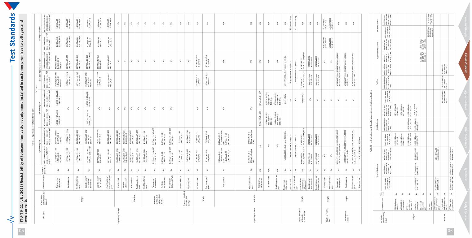
ITU-T�K.21��(J
UL�20
19)�R
esistibi
lity�of
�teleco
mmun
icat
ion�eq
uipm
ent�ins
talled
�in�cus
tomer
�pre
mises
�to�vol
tage
s�an
d�ov
ercu
rren
ts�
Environmental�AnalysisChoose�a�Standard
Application�GuideSelect�Components
System�TestApply�&�Optimize
Test��Stand
ards
Tabl
e�1a
�‒�App
licab
le�te
sts�f
or�exter
nal�p
orts
Test�ty
peBa
sic�te
st�le
vels�(a
lso�
see�clau
se�7�of�[IT
U-T�
K.44
])
No.�of�p
airs�
simul
tane
ously�
tested
Test�con
nections
Port�ty
pe
Symmet
ric�po
rtSy
mmet
ric�po
rtDed
icat
ed�pow
er�fe
ed�por
tMains
�pow
er�por
tPr
imar
ypr
otec
tion
Enha
nced
�test�le
vels
�(also�se
e�clau
ses�5
�an
d�7�of
�[ITU
-T�K.44]
)
Basic�te
st�le
vels�
(also�se
e�clau
se�7�of
�[ITU
-T�K.44]
)
Enha
nced
�test�le
vels
�(also�se
e�clau
ses�5
�an
d�7�of
�[ITU
-T�K.44]
)
Basic�te
st�le
vels
�(also�se
e�clau
se�7�of
�[ITU
-T�K.44]
)
Enha
nced
�test�le
vels�
(also�se
e�clau
ses�5
�and
�7�of�[IT
U-T�K.44]
)
Basic�te
st�le
vels
�(also�se
e�clau
se�7�of�
[ITU
-T�K.44]
)
Enha
nced
�test�le
vels
�(also�se
e�clau
ses�5
�and
�7�of�[IT
U-T�K.44]
)
Sing
le
Tran
sver
se/�
diffe
rent
ial
No
No
No
Port�to
�ear
th
Coor
dina
tion
/Tr
ansv
erse
/�di
ffere
ntial
Coor
dina
tion
/Po
rt�to
�ear
th
Port�to
�exter
nal�
port
Coor
dina
tion
/Po
rt�to
�exter
nal�
port
Yes
Yes
Yes
10/7
00μs
�15+
25Ω
1.5K
V�A.
6.1-
1�(a�and
�b)
10/7
00μs
�15+
25Ω
1.5K
V�A.
6.1-
2�
10/7
00μs
�15+
25Ω
1.5K
V�A.
6.1-
3�
10/7
00μs
�15+
25Ω
4KV�A.
6.1-
1�(a�and
�b)
10/7
00μs
�15+
25Ω
4KV�A.
6.1-
2�
10/7
00μs
�15+
25Ω
4KV�A.
6.1-
3�
10/7
00μs
�15+
25Ω
1.5K
V�A.
6.1-
1�(a�and
�b)
10/7
00μs
�15+
25Ω
6KV�A.
6.1-
2�
10/7
00μs
�15+
25Ω
6KV�A.
6.1-
3�
10/7
00μs
�15+
25Ω
6KV�A.
6.1-
1�(a�and
�b)
10/7
00μs
�15+
25Ω
6KV�A.
6.1-
2�
10/7
00μs
�15+
25Ω
6KV�A.
6.1-
3�
1.2/
50�‒�8/2
0μs�2
Ω1K
V�A.
6.2-
11.2/
50�‒�8/2
0μs�2
Ω1.5K
V�A.
6.2-
1
n/a
n/a
1.2/
50�‒�8/2
0μs�2
Ω4K
V�A.
6.2-
11.2/
50�‒�8/2
0μs�2
Ω6K
V�A.
6.2-
1
n/a
n/a
10/7
00μs
�15+
25Ω
1.5K
V�A.
6.3-
1�(a�and
�b)
10/7
00μs
�15+
25Ω
1.5K
V�A.
6.3-
2�
10/7
00μs
�15+
25Ω
1.5K
V�A.
6.3-
3�
10/7
00μs
�15+
25Ω
4KV�A.
6.3-
1�(a�and
�b)
10/7
00μs
�15+
25Ω
4KV�A.
6.3-
2�
10/7
00μs
�15+
25Ω
4KV�A.
6.3-
3�
10/7
00μs
�15+
25Ω
1.5K
V�A.
6.3-
1�(a�and
�b)
10/7
00μs
�15+
25Ω
6KV�A.
6.3-
2�
10/7
00μs
�15+
25Ω
6KV�A.
6.3-
3�
10/7
00μs
�15+
25Ω
6KV�A.
6.3-
1�(a�and
�b)
10/7
00μs
�15+
25Ω
6KV�A.
6.3-
2�
10/7
00μs
�15+
25Ω
6KV�A.
6.3-
3�
1.2/
50μs
�2Ω
2.5K
V�A.
6.4-
1
1.2/
50μs
�2Ω
2.5K
V�A.
6.4-
2
1.2/
50μs
�2Ω
2.5K
V�A.
6.4-
3
1.2/
50μs
�2Ω
6KV�A.
6.4-
1
1.2/
50μs
�2Ω
6KV�A.
6.4-
2
1.2/
50μs
�2Ω
6KV�A.
6.4-
3
1.2/
50μs
�2Ω
6KV�A.
6.4-
1
1.2/
50μs
�2Ω
6KV�A.
6.4-
2
1.2/
50μs
�2Ω
6KV�A.
6.4-
3
1.2/
50μs
�2Ω
10KV
�A.6.4-1
1.2/
50μs
�2Ω
10KV
�A.6.4-2
1.2/
50μs
�2Ω
10KV
�A.6.4-3
Ligh
tnin
g/�vol
tage
Mul
tipl
e
Port�to
�ear
th
Port�to
�xter
nal�p
ort
Port�to
�ear
th
Port�to
�exter
nal�
port
No
No
Yes
Yes
10/7
00μs
�15+
25Ω
1.5K
V�A.
6.1-
4
10/7
00μs
�15+
25Ω
1.5K
V�A.
6.1-
5
10/7
00μs
�15+
25Ω
4KV�A.
6.1-
4
10/7
00μs
�15+
25Ω
4KV�A.
6.1-
5
10/7
00μs
�15+
25Ω
1.5K
V�A.
6.1-
4
10/7
00μs
�15+
25Ω
1.5K
V�A.
6.1-
5
10/7
00μs
�15+
25Ω
6KV�A.
6.1-
4
10/7
00μs
�15+
25Ω
6KV�A.
6.1-
5
n/a
n/a
n/a
n/a
n/a
n/a
n/a
n/a
n/a
n/a
n/a
n/a
Ethe
rnet�
nshielde
d�tw
iste
d�pa
ir�
(UTP
E)
Port�to
�exter
nal�
port Tran
sver
se/�
diffe
rent
ial
Voltag
e�im
pulse�te
st
Power
�ove
r�Et
hern
et�(P
oE)
No
No
No
No
1.2/
50μs
�2+1
0Ω2.5K
V�A.
6.7-
4
1.2/
50μs
�2+1
0Ω+1
0Ω2.5K
V�A.
6.7-
5
1.2/
50μs
�2+5
Ω2.5K
V�A.
6.7-
3a
1.2/
50μs
�2+1
0Ω+1
0Ω2.5K
V�A.
6.7-
2
1.2/
50μs
�2+1
0Ω6K
V�A.
6.7-
4
1.2/
50μs
�2+1
0Ω+1
0Ω6K
V�A.
6.7-
5
1.2/
50μs
�2+5
Ω6K
V�A.
6.7-
3a
1.2/
50μs
�2+1
0Ω+1
0Ω6K
V�A.
6.7-
2
n/a
n/a
n/a
n/a
n/a
n/a
n/a
n/a
n/a
n/a
n/a
n/a
Ethe
rnet�shielde
d�tw
iste
d�pa
ir�
(STP
E)
Shield�to
�ear
th
Port�to
�ear
th
No
No
1.2/
50μs
�2+5
Ω2.5K
V�A.
6.7-
6
1.2/
50μs
�2+1
0Ω2.5K
V�A.
6.7-
4
1.2/
50μs
�2+5
Ω6K
V�A.
6.7-
6
1.2/
50μs
�2+1
0Ω2.5K
V�A.
6.7-
4
n/a
n/a
n/a
n/a
Ligh
tnin
g�cu
rren
t
Sing
le
Port�to
�ear
th
Port�to
�exter
nal�
port
No
No
8/20
μs�A.6.1-2�
1�kA
/wire
8/20
μs�A.6.1-3�
1�kA
/wire
8/20
μs�A.6.1-2
�5�kA/
wire
8/20
μs�A.6.1-3�
5�kA
/wire
n/a
n/a
8/20
μs�A.6.3-2�
1�kA
/wire
8/20
μs�A.6.3-3
1�kA
/wire
8/20
μs�A.6.3-2
�5�kA/
wire
8/20
μs�A.6.3-3
�5�kA/
wire
n/a
n/a
Mul
tipl
e
Port�to
�ear
th
Port�to
�exter
nal�
port Tran
sver
se/�
diffe
rent
ial
Shield�to
�ear
th
Shield�to
�exter
nal�
port
No
No
n/a
n/a
n/a
8/20
μs�A.6.1-4�
1�kA
/wire�lim
ited
�6K
A1.2/
50μs
�2+5
Ω2.5K
V�A.
6.7-
3a
8/20
μs�A.6.1-4�
5�kA
/wire�lim
ited
�30
KA1.2/
50μs
�2+5
Ω6K
V�A.
6.7-
3a
8/20
μs�A.6.1-5�
1�kA
/wire�lim
ited
�6K
A
8/20
μs�A.6.1-5�
5�kA
/wire�lim
ited
�30
KA
n/a
n/a
n/a
n/a
n/a
�8/2
0μs�A
.6.2-1�1�kA
�8/2
0μs�A
.6.2-1�5�kA
�8/2
0μs��A.
6.2-
2�塔
上设
备�4KA
其他2K
A
�8/2
0μs
A.6
.2-2
塔上
设备�2
0K
A
其他��5
KA
�8/2
0μs
A.6
.2-3
塔上
设备�4
KA
其他
2K
A
8/20
μs
A.6
.2-3
塔上
设备�2
0K
A
其他��5
KA
n/a
n/a
n/a
n/a
n/a
n/a
n/a
n/a
n/a
n/a
Power
�indu
ction�
and�ea
rth�
pote
ntial�rise
Sing
le
Tran
sver
se/�
diffe
rent
ial
Port�to
�ear
th
Port�to
�exter
nal�
port
Coor
dina
tion
�Tr
ansv
erse
/�di
ffere
ntial
Coor
dina
tion
�po
rt�to
�ear
th
Coor
dina
tion
�por
t�to
�exter
nal�p
ort
No
No
No
Yes
Yes
Yes
AC60
0V60
0Ω�A.6.1-1
(a�and
�b)�t
=0.2s
AC60
0V60
0Ω�A.6.1-2�t=
0.2s
AC60
0V60
0Ω�A.6.1-3�t=
0.2s
AC60
0V60
0Ω�
A.6.1-
1(a�an
d�b)
�t=1s
AC60
0V60
0Ω�
A.6.1-
2�t=
1s
AC60
0V60
0Ω�
A.6.1-
3�t=
1s
AC15
00V2
00Ω�
A.6.1-
1(a�an
d�b)
�t=2s
AC15
00V2
00Ω�
A.6.1-
2�t=
2s
AC15
00V2
00Ω�
A.6.1-
3�t=
2s
Und
erstud
y
n/a
n/a
Und
erstud
y
n/a
n/a
AC60
0V60
0Ω A
.6.3
-1(a
an
d b
) t=
0.2
s
AC60
0V60
0Ω A
.6.3
-2 t
=0
.2s
AC60
0V60
0Ω A
.6.3
-3 t
=0
.2s
AC60
0V60
0ΩA
.6.3
-1(a
an
d b
) t=
1s
AC60
0V60
0Ω
A.6
.3-2
t=
1s
AC60
0V60
0Ω
A.6
.3-3
t=
1s
AC15
00V2
00Ω�
A.6.3-
1(a�an
d�b)
�t=2s
AC15
00V2
00Ω�
A.6.3-
2�t=
2s
AC15
00V2
00Ω�
A.6.3-
3�t=
2s
n/a
5.2.1�un
der�s
tudy
5.2.1�un
der�s
tudy
n/a
n/a
n/a
Neu
tral�pot
ential�
rise
Sing
le
Port�to
�ear
th
Port�to
�exter
nal�
port
No
No
n/a
n/a
n/a
n/a
AC60
0V60
0Ω
A.6
.4-2
t=
1s
AC60
0V60
0Ω
A.6
.4-3
t=
1s
AC15
00V2
00Ω
A
.6.4
-2 t
=1
s
AC15
00V2
00Ω
A
.6.4
-3 t
=1
s
Mains
�pow
er�
cont
act
Sing
le
Tran
sver
se/�
diffe
rent
ial
Port�to
�ear
th
Port�to
�exter
nal�
port
Ethe
rnet�por
t
No
No
No
No
AC23
0V10
/20/
40/8
0/16
0/30
0/60
0/10
00Ω
�A.6.1-1
(a�and
�b)�t
=15m
in
AC23
0V10
/20/
40/8
0/16
0/30
0/60
0/10
00Ω�
A.6.1-
2�t=
15min
AC23
0V10
/20/
40/8
0/16
0/30
0/60
0/10
00��
A.6.1-
3�t=
15min
�A.6.7-3��5
00V�DC���⼤
于2M
Ω
n/a
n/a
n/a
n/a
n/a
AC23
0V10
/20/
40/8
0/16
0/30
0/60
0/10
00Ω
A
.6.3
-1(a
an
d b
) t=
15
min
AC23
0V10
/20/
40/8
0/16
0/30
0/60
0/10
00Ω
A
.6.3
-2 t
=1
5m
in
AC23
0V10
/20/
40/8
0/16
0/30
0/60
0/10
00Ω
A
.6.3
-3 t
=1
5m
in
n/a
n/a
n/a
�Tab
le�1b�‒�Ligh
tnin
g�te
st�con
dition
s�for
�por
ts�con
nected
�to�in
tern
al�cab
les
No.�o
f�pairs�
simul
tane
ously
tested
Test�con
nection�
Prima
rypro
tectio
n
Uns
hielde
d�ca
ble
Shield
ed�cab
lePo
E�feed
DC�po
wer
ed�equ
ipmen
tDC�po
wer
�sou
rce
Sing
le
�Mul
tipl
e
Shield
ed�cab
le�
to�ear
th
USB
�shielde
d�ca
ble�to
�ear
th�
STPE
�simul
tane
ous�
port�to
�ear
th�
UTP
E/ST
PE�
tran
sver
se�
DC�po
wer
ed�
equipm
ent�
port�
DC�po
wer
�so
urce
�por
t�
No
No
No
No
No
No
1.2/
50-8
/20μ
s2Ω�
2.5K
V�A.
6.7-
51.2/
50-8
/20μ
s2Ω�
4KV�A.
6.7-
5
Basic�te
st�le
vels
�(also�se
e�clau
se�
7�of
�[ITU
-T�K.44]
)
Inte
rmed
iate�
test�le
vels�(a
lso�
see�clau
se�7�of�
[ITU
-T�K.44]
)
Enha
nced
�test�
leve
ls�(a
lso�se
e�clau
ses�5
�and
�7�of
�[ITU
-T�K.44]
)
Basic�te
st�le
vels
�(also�se
e�clau
se�7�of�[IT
U-T�K.44]
)
Inte
rmed
iate�te
st�
leve
ls�(a
lso�se
e�claus
e�7�of
�[ITU
-T�K.44]
)
Enha
nced
�test�
leve
ls�(a
lso�se
e�clau
ses�5
�and
�7�
of�[ITU
-T�K.44]
)
Basic�te
st�le
vels
�(also�se
e�clau
se�7�of�[IT
U-T�K.44]
)
Inte
rmed
iate�te
st�
leve
ls�(a
lso�se
e�clau
se�7�of�[IT
U-T
�K.44]
)
Enha
nced
�test�
leve
ls�(a
lso�se
e�claus
es�5�and
�7�
of�[ITU
-T�K.44]
)
Basic�te
st�
leve
ls�(a
lso�
see�clau
se�7�
of�[ITU
-T�K.44]
)
Enha
nced
�test�
leve
ls�(a
lso�se
e�claus
es�5�and
�7�of�[IT
U-T�K.44]
)Basic�te
st�le
vels�
(also�se
e�clau
se�7�of�[IT
U-T�K.44]
)Enha
nced
�test�
leve
ls�(a
lso�se
e�clau
ses�5
�and
�7�of�[IT
U-T�K.44]
)
Uns
hielde
d�ca
ble�
with�sy
mmet
ric�
pairs�
PoE�Mod
e�A�an
d�Mod
e�B�tran
sver
sete
stin
g�
UTP
E�po
rt�ra
ted�
impu
lse�vo
ltag
e
No
No
No
1.2/
50-8
/20μ
s2Ω+
10Ω�1KV
�A.6.5-1
1.2/
50-8
/20μ
s2Ω+
5Ω�2.5KV
�A.6.7-3
a1.2/
50-8
/20μ
s2Ω+
5Ω�4KV
�A.6.7-3
a
1.2/
50-8
/20μ
s2Ω+
10Ω�1.5KV
�A.6.5-1
1.2/
50-8
/20μ
s2Ω+
5Ω�6KV
�A.6.7-3
a
1.2/
50-8
/20μ
s2Ω�
6KV�A.
6.7-
5
1.2/
50-8
/20μ
s2Ω
�1KV
�A.6.5-2
1.2/
50-8
/20μ
s2Ω
100V
�A.6.5-2
1.2/
50-8
/20μ
s2Ω+
5��2
.5KV
�A.6.7-6
1.2/
50-8
/20μ
s2Ω�
2.5K
V�A.
6.7-
5
1.2/
50-8
/20μ
s2Ω
+5Ω�4KV
�A.6.7-6
1.2/
50-8
/20μ
s2Ω�
4KV�A.
6.7-
5
1.2/
50-8
/20μ
s2Ω
1.5K
V�A.
6.5-
2
1.2/
50-8
/20μ
s2Ω
�150
V�A.
6.5-
2
1.2/
50-8
/20μ
s2Ω+
5Ω�6KV
�A.6.7-6
1.2/
50-8
/20μ
s2Ω�
6KV�A.
6.7-
5
B1.2/5
0-8/
20μs
2Ω+1
0Ω�+10
Ω2.5K
V�A.
6.7-
2
1.2/
50-8
/20μ
s2Ω+
10Ω�+10
Ω4K
V�A.
6.7-
2
1.2/
50-8
/20μ
s2Ω
+10Ω
�+10
Ω6K
V�A.
6.7-
2
1.2/
50-8
/20μ
s2Ω
+10Ω
�+9μ
F1K
V�A.
6.6-
1a
1.2/
50-8
/20μ
s2Ω
+10Ω
�+9μ
F1.5K
V�A.
6.6-
1a
1.2/
50-8
/20μ
s2Ω
+10Ω
�+9μ
F1K
V�A.
6.6-
1b
1.2/
50-8
/20μ
s2
Ω+
10
Ω +
9μ
F1
.5K
V A
.6.6
-1b

GR1
089-
2:(2
010)�Electro
mag
netic�Co
mpa
tibi
lity�(E
MC)
�and
�Electrica
l�Saf
ety�-�G
ener
ic�Crite
ria�fo
r�Net
wor
k�Te
leco
mmun
icat
ions
�Equ
ipmen
t
Ante
nna�Po
rt�w
ith�Se
cond
ary�
Prot
ecto
r�Tes
t
Ante
nna�Po
rt Te
st
7 8 8.1 9 9.1
10 10.1 11 11.1 12 12.1 13 13.1
14 14.1 15 15.1
16 17 18 19 19.1
High�Ligh
tning�Ex
posu
reTe
st�
for�R
emot
e�OSP
�Inte
r�fac
es50
�(at�4
00�V)�to
500(at�400
0�V)
±40
0�to
�±40
0010
/250
�N/A�
5�at�eac
h�vo
ltage
increm
ent
B
Intra-
Build
ing�with�up
�to2�Pa
irs�p
er�Por
t�(Metallic
)±80
0�10
0�2/
10�
N/A�
Repe
tition
s�eac
h�polar
ity�may
�be�
5�on
�1�sam
ple,�or�
1�on
�3�sam
ples
.
A1,�A
2,�A3,A4
Intra-
Build
ing�with�Se
cond
ary�
Prot
ecto
rs�up�to
�2�Pairs�per�
Port�(M
etallic
)±Vs
100
(at�8
00�V)
2/10
N/A�
Repe
tition
s�eac
h�po
larity�m
ay�be�5
on�1�sam
ple,�or�1
�on
�3�sam
ples
.
A1,�A
2,�A3,A4
Intra-
Build
ing�with�up
�to2�Pa
irs�p
er�Por
t�(Lon
gitu
dina
l)±15
0010
0�2/
10�
N/A�
Repe
tition
s�eac
h�po
larity�m
ay�be�5
on�1�sam
ple,�or�1
�on
�3�sam
ples
.
B
Intra-
build
ing�with�Se
cond
ary�
Prot
ecto
rs�up�to
�2�Pairs�per�
Port�(L
ongitu
dina
l)±Vs
100
(at�1
500�V)
2/10
�N/A�
Repe
tition
s�eac
h�po
larity�m
ay�be�5
on�1�sam
ple,�or�1
�on
�3�sam
ples
.
B
Alte
rnat
ive�Intra-
Build
ing�fo
r�up
�to�2�Pairs�per�Por
t�(Metallic
)±80
0�40
0�1.2/
50-8/2�0
6�
Repe
tition
s�eac
h�po
larity�m
ay�be�5�
on�1�sam
ple,�or�1
�on
�3�sam
ples
.
A1,�A
2,�A3,A4
Alte
rnat
ive�Intra-
Build
ing�with�
Seco
ndar
y�Pr
otec
tors�up�to
�2�
Pairs�p
er�Por
t�(Metallic
)±Vs
�Vs
/2�1.2/
50-8/2�0
6�
Repe
tition
s�eac
h�po
larity�m
ay�be�5�
on�1�sam
ple,�or�1
�on
�3�sam
ples
.
A1,�A
2,�A3,A4
Alte
rnat
ive�Intra-
Build
ing�up
�to�
2�Pa
irs�p
er�Por
t�(Lo
ngitud
inal)
±15
00�
750�
1.2/
50-8/2
0�10
�
Repe
tition
s�eac
h�po
larity�m
ay�be�5�
on�1�sam
ple,�or�
1�on
�3�sam
ples
.
B
Alte
rnat
ive�Intra-
Build
ing�
Und
ervo
ltage
�up�to
�2�Pairs�
per�P
ort(Lo
ngitud
inal)
±Vs
�Vs
/2�1.2/
50-8/2
0�10
�
Repe
tition
s�eac
h�po
larity�m
ay�be�5�
on�1�sam
ple,�or�1
�on
�3�sam
ples
.
B
Intra-
Build
ing�fo
r�3�or�4
�Pa
irs�p
er�Por
t�(Metallic
)±80
0�40
06�
Repe
tition
s�eac
h�po
larity�m
ay�be�5�
on�1�sam
ple,�or�1
�on
�3�sam
ples
.
Test�per
Figu
re�4-10
Intra-
Build
ing�with�Se
cond
ary�
Prot
ecto
rs,�3
�or�4
�Pairs�per�
Port�(M
etallic
)±Vs
�Vs
/26�
Repe
tition
s�eac
h�po
larity�m
ay�be�5�
on�1�sam
ple,�or�1
�on
�3�sam
ples
.
Test�per
Figu
re�4-10
Intra-
Build
ing�3�or
�4�Pairs�
per�P
ort�(Lo
ngitud
inal)
±15
00�
750�
20�
Repe
tition
s�eac
h�po
larity�m
ay�be�5�
on�1�sam
ple,�or�1
�on
�3�sam
ples
.
B
Intra-
Build
ing�Und
ervo
ltage
�3�or
�4�Pairs�per�Por
t�(Lon
gitu
dina
l)±Vs
�Vs
/220
�
Repe
tition
s�eac
h�po
larity�m
ay�be�5�
on�1�sam
ple,�or�1
�on
�3�sam
ples
.
Intra-
Build
ing�fo
r�>�4�Pairs�
per�P
ort(Metallic
)±80
0�40
06�
Repe
tition
s�eac
h�po
larity�m
ay�be�5�
on�1�sam
ple,�or�1
�on
�3�sam
ples
.
B
Test�per
Figu
re�4-10
Intra-
Build
ing�with�Se
cond
ary�
Prot
ecto
rs,�>
�4�Pairs�per�
Port�(M
etallic
)±Vs
�Vs
/26�
Repe
tition
s�eac
h�po
larity�m
ay�be�5�
on�1�sam
ple,�or�1
�on
�3�sam
ples
.
Test�per
Figu
re�4-10
Intra-
Build
ing�fo
r�>�4�Pairs�
per�P
ort(Lo
ngitud
inal)
±15
00�
750�
40�
Repe
tition
s�eac
h�po
larity�m
ay�be�5�
on�1�sam
ple,�or�1
�on
�3�sam
ples
.
B
Intra-
Build
ing�with�Se
cond
ary�
Prot
ecto
rs�fo
r�>�4�Pairs�per�
Port(Lon
gitu
dina
l)±Vs
�Vs
/240
�
Repe
tition
s�eac
h�po
larity�m
ay�be�5�
on�1�sam
ple,�or�1
�on
�3�sam
ples
.
B
Intra-
Build
ing�fo
r�Paire
d�Sh
ielded
�Cab
les
±15
00�
750�
2�
Repe
tition
s�eac
h�po
larity�m
ay�be�5�
on�1�sam
ple,�or�1
�on
�3�sam
ples
.
See�Figu
re�4-12
Intra-
Build
ing�fo
r�Coa
xial
±15
00�
750�
2
Repe
tition
s�eac
h�po
larity�m
ay�be�5�
on�1�sam
ple,�or�1
�on
�3�sam
ples
.
See�Figu
re�4-13
Custom
er�Side�ONT�Inte
rfac
es±10
00�
100�
10/1
000�
N/A�
5�A5
,�A6�
±60
0�30
0�N/A�
5�Ce
nter�con
ductor
�to
�shield�
±Vs
�30
0(at�600
�V)�
N/A�
5�Ce
nter�con
ductor
�to
�shield�
�1.2/
50-8/2
0�
�1.2/
50-8/2
0�
�1.2/
50-8/2
0�
�1.2/
50-8/2
0�
�1.2/
50-8/2
0�
�1.2/
50-8/2
0�
�1.2/
50-8/2
0�
�1.2/
50-8/2
0�
�1.2/
50-8/2
0�
�1.2/
50-8/2
0�
�1.2/
50-8/2
0�
�1.2/
50-8/2
0�
3,5
2,3a
/5a,4,4a
2,3a
/5a,4,4a
2,4,4a
2,4,4a
2,3a
/5a,4,4a
2,3a
/5a,4,4a
2,4,4a
2,4,4a
2,3a
/5a,4,4a
2,3a
/5a,4,4a
2,4,4a
2,4,4a
2,3a
/5a,4,4a
2,3a
/5a,4,4a
2,4,4a
2,4,4a
2,3a
/5a,4,4a
2,3a
/5a,4,4a
4a 6 6
1=CO
�OSP
�Cab
le�Por
ts,���������2
=CO�In
tra-
build
ing�Ca
ble�Po
rts,�������3
=CO�In
tra-
build
ing�Ca
ble�Po
rts,������3
a/5a
=Non
-CO�In
tra-
Build
ing�Po
rts,�����3b/
5b=S
hort�Rea
ch�O
SP�Cab
le�Por
ts,�����4
=Int
ra-C
ell�S
ite�Cab
le�Por
ts,
4a=C
usto
mer
-Side�Opt
ical�Net
wor
k�Te
rminals�(
ONTs
)�and
�Inte
llige
nt�Net
wor
k�Inte
rfac
e�De
vice
s�(iN
IDs)�Cab
le�Por
ts,�����5
=OSP
�Site
�OSP
�Cab
le�Por
ts,�����6
=Ant
enna
�Por
ts�,�����7
=AC�Po
wer�Por
ts,
8a=D
C�Po
wer�to
�Ant
enna
,�����8
b=Intra-
Cell�Site�DC�Po
wer
1=CO
�OSP
�Cab
le�Por
ts,��3
=CO�In
tra-
build
ing�Ca
ble�Po
rts,��5
=OSP
�Site
�OSP
�Cab
le�Por
ts,����7=A
C�Po
wer�Por
ts,
AC�Pow
er�Por
t�Tes
t�with�
Exte
rnal�SPD
AC�Pow
er�Por
t�Tes
t�with�
Exte
rnal�SPD
AC�Pow
er�Por
t�with�Se
cond
ary�
Prot
ecto
r
Tower�M
ount
ed�Tra
nsce
iver�Fed
�with�Re
mot
e�DC
�Pow
er�Tes
t�(Lon
gitu
dina
l)
1 1.1
1.2 2 2.1
2.2 3 4 5 6 20 21 21.1 22 23
Surg
eTe
stNum
ber
Port�Typ
esTe
st�Des
cription
Min.Pea
k�Ope
n-Ci
rcuitV
olta
ge�
(Volts)
Min.�P
eak�Sh
ort-
Circuit�C
urre
nt�per�
Cond
ucto
r�(Am
pere
s)
Surg
e�Max
imum
Rise
/Minim
umDe
cay�Timefor
�Vo
ltage
�and
�Cur
rent
(μs)
Value�of
Exte
rnal
Non
-Indu
ctive
Resistor
s
Repe
tition
s�Eac
hPo
larity
Test�Con
nections
First-Le
vel�L
ight
ning
�Sur
ge���������
���������
1,3,3b
/5b,5
Multipo
rt�O
SP�Tes
t�±10
00���
25����
10/3
60����
N/A����
5����
Up�to
�24
cond
ucto
rs
Shor
t�Loo
p�OSP
�Inte
rfac
e±10
00���
25����
10/3
60����
N/A����
5����
A����
Shor
t�Loo
p�OSP
�Inte
rfac
e�-�
with�Se
cond
ary�Pr
otec
tors
10/3
60����
N/A����
5����
A����
±Vs
�25
(at�1
000�V)
�OSP
�Inte
rfac
e�±10
0�to
�±10
00�
10(at�1
00�V)to�
100(at�100
0�V)�
10/1
000�
N/A�
5�at�eac
h�vo
ltage
increm
ent�
A
Exte
nded
�OSP
�Inte
rfac
e±10
0�to
�±20
00�
10(at�1
00�V)to�
100(at�200
0�V)�
10/1
000�
N/A�
5�at�eac
h�vo
ltage
increm
ent�
A
OSP
�Inte
rfac
e‒with�
Seco
ndar
yPro
tector
s±Vs
100(at�100
0�V)
N/A����
5����
A����
10/1
000�
Gas
�Tub
e�Inte
raction�Te
st�
±40
00�
SeeF
igur
e�4-6
10/7
00�volta
ge5/
310�cu
rren
t25
�5�
(A5�an
d�A6
)�orB
Indu
ctive�Ki
ck�Tes
t�for
�OSP
�Inte
rfac
es±25
00�
500�
2/10
�N/A�
10�
See�Figu
re�4-1�
Fast�Rise�Time�Te
st�fo
r�Re
mot
e�OSP
�Inte
rfac
es±10
00�
200�
2/10
N/A�
5�A�
Highe
r�Gro
und�Re
sistan
cefo
r�Re
mot
e�OSP
�Inte
rfac
es�‒
Long
itud
inal
±10
00�
100�
10/1
000�
N/A�
5�A5
,�A6�
±20
00�
1000
�N/A�
5�
±60
00�
3000
�N/A�
5�
±Vs
�30
00(at�6
000�V)�
N/A�
5�
±60
00�
Minim
um�pea
k�sh
ort-circuit�c
urre
nt�
per�p
ort�is�3
000�A.�
N/A�
5�Se
e�Figur
e�4-15.�Fee
d�an
d�re
turn
�to�shield�
simulta
neou
sly
Phas
e�to
�neu
tral,�
phas
e�to
�gro
und,
neut
ral�to�gr
ound
Phas
e�to
�neu
tral,�
phas
e�to
�gro
und,
neut
ral�to�gr
ound
Phas
e�to
�neu
tral,�
phas
e�to
�gro
und,
neut
ral�to�gr
ound
±25
00�
Minim
um�pea
k�sh
ort-
circuit�c
urre
nt�per
port�is
�500
0�A.�
8/20
curren
t�N/A�
5�B�
Volta
ge�Lim
iting�fo
r�Int
ra-S
ite�
Cell�Site�Por
ts�(L
ongitu
dina
l)
Seco
nd-Lev
el�Light
ning
�Sur
ge
Surg
e�Tes
tNum
ber�
1� 2� 2.1�
Port�Typ
esTe
st�Des
cription
Min.Pea
k�Ope
n-Ci
rcuit
Volta
ge(Volts)
Indu
ctive�Ki
ck�Tes
t�for
�OSP
�Inte
rfac
es
Min.�P
eak�Sh
ort-Ci
rcuit�
Curren
t�per�Con
ductor
(Ampe
res)
Surg
e�Max
imum
�Rise/
Minim
umDe
cayT
imefor
�Volta
gean
d�Cu
rren
t(μs
)
Repe
tition
s�Eac
hPo
larity
Test�Con
nections
Ligh
tning�to
�AC�
Power�Por
t�
Ligh
tning�to
�AC�Po
wer�
Port�W
ith�Se
cond
ary�
Prot
ecto
rs�
±50
00�
±60
00�
±Vs
�
500�
3000
�
3000
(at�6
000�V)�
2/10
�
1.2/
50-8/2
0�
1.2/
50-8/2
0�
1 1 1
Phas
e�co
nduc
tors�to
�neu
tral,�
phas
e�co
nduc
tors�to
�gro
und,
neut
ral�c
ondu
ctor
�to�gro
und
Phas
e�co
nduc
tors�to
�neu
tral,�
phas
e�co
nduc
tors�to
�gro
und,
neut
ral�c
ondu
ctor
�to�gro
und
See�Figu
re�4-1
�1.2/
50-8/2
0�
�1.2/
50-8/2
0�
�1.2/
50-8/2
0�
�1.2/
50-8/2
0�
3b/5
b
3b/5
b
1,3,5
1,3,5
1,3,3b
/5b,5
1,3,5
3,5
3,3b
/5b,5
3,5 7 7 7 8a
3a/5
a,8b
7 7
1,3,5
07 08
Environmental�AnalysisChoose�a�Standard
Application�GuideSelect�Components
System�TestApply�&�Optimize
Test��Stand
ards

IEC61000-4-5:2014��Electromagnetic�compatibility�(EMC)�‒Part�4-5:�Testing�and�measurement�techniques�‒�Surge�immunity�test
Test�levels�(kV)
Installationclass�
Unsymmetricaloperated
a,d,ecircuits/lines
Symmetricaloperated
a,d,ecircuits/lines
Shieldeda,d,fcircuits/lines
AC�powersupply�anda.c.�I/O
DC�power�supplyand�d.c.�I/O
aExternal�ports a,dInternal�ports External�port Internal�port External�port Internal�portaExternal�ports a,dInternal�ports External�port Internal�port
Line�toline
Line�toground
Line�toline
Line�toground
Line�toline
Line�toground
Line�toline
Line�toground
Line�toline
Line�toground
Line�toline
Line�toground
Line�toline
Line�toground
Line�toline
Line�toground
Line�toline
Line�toground
Line�toline
Line�toground
0�
1� 0.5 0.50.5
2 0.5 1.0 1.0 0.51.00.5�
3 1.0 2.0 2.0 2.02.01.02.01.0�
4�� b2.0 �� b4.0 �� b2.0 � b4.0 � b2.0 �� b4.0 �� b2.0 �� b4.0 b2.0 �� b4.0 �� b2.0 �� b4.0 b4.0 b4.0 b4.0 b4.0
5� c,b�� b2.0 �� b4.0 �� b2.0 �� b4.0 � b2.0 �� b4.0c,b�� b2.0 �� b4.0 �� b2.0 �� b4.0 b4.0 b4.0 b4.0 b4.0
a:��No�test�is�advised�if�the�cable�length�is�shorter�than�or�equal�to�10�m.b:��Where�the�port�is�always�intended�to�be�used�with�specified�primary�protection,�testing�is�performed�with�the�primary�protection�in�place�to�ensure�coordination�with�the������protection�elements.�If�primary�protection�is�required�to�protect�the�interface�but�not�provided,�testing�is�also�performed�at�the�maximum�let�through�level�of�the�specified������primary�protection�and�with�a�typical�primary�protector.c:��Depends�on�the�class�of�the�local�power�supply�system.d:��The�testing�of�intra-system�ports�is�generally�not�required.e:��Line-to-line�surges�(transverse)�may�occur�in�networks�where�SPDs�(surge�protective�devices)�with�connection�to�ground�are�used�for�protection.�Such�surges�are�outside�the������scope�of�this�standard.�This�phenomenon�can�however�be�simulated�by�applying�common�mode�surges�through�the�defined�primary�protection�elements.f:��The�testing�of�ports�connecting�to�antennas�is�outside�the�scope�of�this�standard.
Open�circuit�output�test�voltage�and�repetition�frequency�of�the�impulses
Power�ports,�earth�port�(PE) Signal��and�control�ports
Voltage�peak Repetition�frequency Voltage�peak Repetition�frequencykV kHz kV kHz
Level
1� 0.5� 5�or�100 0.25� 5�or�100
2�
3
4a�X
1�
2�
4�
5�or�100
5�or�100
5�or�100
0.25�
1�
2�
5�or�100
5�or�100
5�or�100
Special Special Special Special
The�use�of�5�kHz�repetition�frequency�is�traditional,�however,�100�kHz�is�closer�to�reality.�Product�committeesshould�determine�which�frequencies�are�relevant�for�specific�products�or�product�types.
With�some�products,�there�may�be�no�clear�distinction�between�power�ports�and�signal�ports,�in�which�case�it�is�up�to�product�committees�to�make�this�determination�for�test�purposes.
a:�"X"�can�be�any�level,�above,�below�or�in�between�the�others.�The�level�shall�be�specified�in�the�dedicatedequipment�specification.
Examples�of�test�pulse�severity�levels�for�nominal�12V�and�24V�system�����������������
a�Test�pulse�
bSelected�test�level��
c,dTest�pulse�severity�level,UsMin.number�of�
pulses�or�test�time��
e��Burst�cycle/pulse�repetition�tim
1�2a�2b�3a�3a�
-150�+112�+10�-220�+150�
-112�+55�+10�-165�+112�
-75�+37�+10�-112�+75�
500Pulses�500Pulses�10Pulses�
1h�1h�
min.�0.5s�0.2s�0.5s�90ms�90ms�
max.�e�
5s�5s�
100ms�100ms�
a:�Test�pulses�as�in�5.6��������b:�Values�agreed�between�vehicle�manufacturer�and�equipment�suppller.��������c:�The�amplitudes�are�the�values�of�Us�as�defined�for�each�test�pulse�in�5.6.��������d:�The�former�levels�I�and�II�are�revised�because�they�did�not�ensure�sufficient�immunity�in�subsequent�road�vehicles'design.��������e:�The�maximum�pulse�repetition�time�shall�be�chosen�such�that�it�is�the�minimum�time�for�the�DUT�to�be�correctly�initialized�before�the�application�of�the�����next�pulse�and�shall�be�≥0.5S.��������
-600�+112�+20�-300�+300�
-450+55�+20�-220+220
-300+37�+20�-150+150
(V)IV� III� I/II�
12 24 12 24 12 24
ISO16750-2:2012��Road�vehicles�--�Environmental�conditions�and�testing�for�electrical�and�electronic�equipment�--�part�2:�electrical�loads
Parameter
Level
Voltage
Duration
Minimum�functional�status
12V 24V 12V 24V 12V 24V 12V
I� II� III� IV
V
ms
US6��� 8(-0.2)��� 4.5(-0.2)��� 3(-0.2)��� 6(-0.2)
US� 9.5(-0.2) � 6.5(-0.2) � 5(-0.2)� 6,5(-0.2)tf� 5(±0.5)� 5(±0.5)� 5(±0.5) � 5(±0.5)t6 � 15(±1.5)� 15(±1.5) � 15(±1.5)� 15(±1.5)t7� 50(±5)� 50(±5)� 50(±5)� 50(±5)t8 � 1000(±100)� 10000(±1000)� 1000(±100)� 10000(±1000)�tr� 40(±4)� 100(±10)� 100(±10) � 100(±10)
a�A aB aB a� Ab�A bB bC bBcB
cC cCdB dC dC
a:��U min�=�6�V;�U max�=�16�V�(see�Table�1,�Code�A).S Sb:��U min�=�8�V;�U max�=�16�V�(see�Table�1,�Code�B).S Sc:��U min�=�9�V;�U max�=�16�V�(see�Table�1,�Code�C).S Sd:��U min�=�10.5�V;�U max�=�16�V�(see�Table�1,�Code�D).s s
10(-0.2)��� 8(-0.2)��� 6(-0.2)
20(-0.2)��� 15(-0.2)��� 10(-0.2)
10(±1)��� 10(±1)��� 10(±1)50(±5)��� 50(±5)��� 50(±5)
50(±5)��� 50(±5)��� 50(±5)1000(±100)��� 1000(±100)��� 1000(±100)
40(±4)��� 100(±10)��� 40(±10)
Parameter
eA � fBgBhB
eBfCgChC
eBfCgChC
cCdC
Type�of�systemMinimum�test�requirements
U =12V��N U =24VN
79≤U ≤101���S 151≤US≤202
0.5≤R≤4i 1≤Ri≤8
40≤t ≤400d
10�pulses�at��1�min��intervals
a:�If�not�otherwise�agreed,�use�the�higher�voltage�level�with�the�higher�value�for�internal�resistance,�or�use�the�lower�voltage�level�with�the�lower�value�for�internal�resistance.
10(�����)0-5 10(�����)0-5
aUs (V)aRi (Ω)
td (ms)
td (ms)
Starting�profile�values�for�systems�with�12V�and�24V�nominal�voltage
e:�U min�=�10�V;�U max�=�32�V�(see�Table�2,�Code�E).S Sf�:�U min�=�16�V;�U max�=�32�V�(see�Table�2,�Code�F).S Sg:�U min�=�22�V;�U max�=�32�V�(see�Table�2,�Code�G).S Sh:�U min�=�18�V;�U max�=�32�V�(see�Table�2,�Code�H).S s
Pulse�for�test�A�in�systems�with�12�V�and�24�V�nominal�voltage
100≤t ≤350d
/� /� /� /� /� /� /� /� /� /� /� /� /� /� /� /� /� /� /� /�
/� /� /� /� /� /� /� /� /� /� /� /� /� /� /� /� /�
/� /� /� /� /� /� /� /� /� /� /� /� /� /�
/� /� /� /� /� /� /� /� /� /� /� /�
/�
/�
/�
/�
/�
/�
/�
/�
ISO7637-2:2011�Road�vehicles�--�Electrical�disturbances�from�conduction�and�coupling--Part�2:�Electrical�transient�conduction�along�supply�lines�only
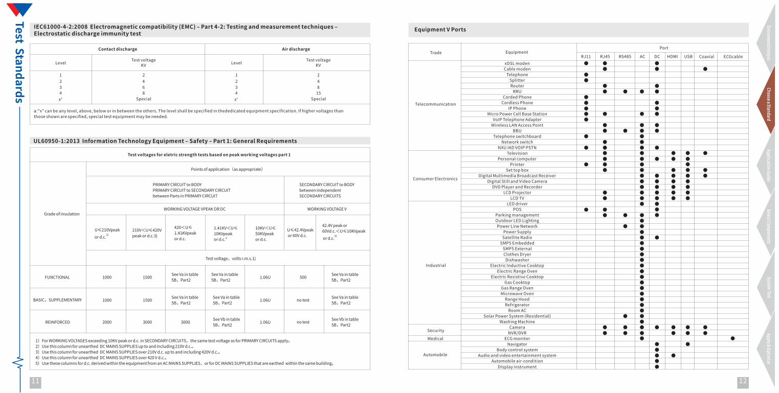
IEC61000-4-4:2012��Electromagnetic�compatibility�(EMC)�‒�Part�4-4:Testing�and�measurement�techniques�‒�Electricalfast��transient/burst�immunity�test
09 10�
Environmental�AnalysisChoose�a�Standard
Application�GuideSelect�Components
System�TestApply�&�Optimize
Test��Standards
Contact�discharge Air�discharge
Level Test�voltageKV Level Test�voltage
KV
1234a�x
2468
Special
234a��x
24815
Special
a:"x"�can�be�any�level,�above,�below�or�in�between�the�others.�The�level�shall�be�specified�in�thededicated�equipment�specification.�If�higher�voltages�than�those�shown�are�specified,�special�test�equipment�may�be�needed.
IEC61000-4-2:2008��Electromagnetic�compatibility�(EMC)�‒�Part�4-2:�Testing�and�measurement�techniques�‒Electrostatic�discharge�immunity�test
UL60950-1:2013��Information�Technology�Equipment�‒�Safety�‒�Part�1:�General�Requirements
Points�of�application(as�appropriate)������������������
PRIMARY�CIRCUIT�to�BODYPRIMARY�CIRCUIT�to�SECONDARY�CIRCUITbetween�Parts�in�PRIMARY�CIRCUIT�����
SECONDARY�CIRCUIT�to�BODYbetween�independentSECONDARY�CIRCUITS���
Grade�of�insulation������
WORKING�VOLTAGE������VPEAK�OR�DC
1)For�WORKING�VOLTAGES�exceeding�10KV�peak�or�d.c.�in�SECONDARY�CIRCUITS,the�same�test�voltage�as�for�PRIMARY�CIRCUITS�apply。����������2)Use�this�column�for�unearthed��DC�MAINS�SUPPLIES�up�to�and�including�210V�d.c.。����������3)Use�this�column�for�unearthed��DC�MAINS�SUPPLIES�over�210V�d.c.�up�to�and�including�420V�d.c.。����������4)Use�this�column�for�unearthed��DC�MAINS�SUPPLIES�over�420�V�d.c.。����������5)Use�these�columns�for�d.c.�derived�within�the�equipment�from�an�AC�MAINS�SUPPLIES,or�for�DC�MAINS�SUPPLIES�that�are�earthed��within�the�same�building。����������
U≤210Vpeak�2)�or�d.c.
�
�
210V<U≤420Vpeak�or�d.c.�3)��
420<U≤1.41KVpeak�or�d.c.���
1.41KV<U≤10KVpeak�
4)�or�d.c.��
10KV<U≤50KVpeak�or�d.c.���
U≤42.4Vpeak�or�60V�d.c.���
42.4V�peak�or�60Vd.c.<U≤10KVpeak
5)���or�d.c.
��
��Test�voltage,volts�r.m.s.1)�����
FUNCTIONAL�
BASIC,SUPPLEMENTARY�
REINFORCED�
1000�
1000�
2000�
1500�
1500�
3000�
See�Va�in�table�5B,Part2�
See�Va�in�table5B,Part2�
3000�
1.06U�
1.06U�
1.06U�
500�
no�test�
no�test�
1
�Test�voltages�for�eletric�strength�tests�based�on�peak�working�voltages�part�1
WORKING�VOLTAGE�V�����
See�Va�in�table�5B,Part2�
See�Va�in�table�5B,Part2�
See�Va�in�table�5B,Part2�
See�Vb�in�table�5B,Part2�
See�Vb�in�table�5B,Part2�
See�Va�in�table�5B,Part2�
Equipment�V�Ports
Equipment
xDSL�modenCable�modenTelephoneSplitterRouterRRU
Corded�PhoneCordless�Phone
IP�PhoneMicro�Power�Cell�Base�Station
VoIP�Telephone�AdapterWireless�LAN�Access�Point
BBUTelephone�switchboard
Network�switchNXU�IAD�VOIP�PSTN
TelevisionPersonal�computer�
PrinterSet�top�box
Digital�Multimedia�Broadcast�ReceiverDigital�Still�and�Video�Camera
DVD�Player�and�RecorderLCD�Projector
LCD�TVLED�driver
POSParking�management�Outdoor�LED�LightingPower�Line�Network
Power�SupplySatellite�Radio
SMPS�EmbeddedSMPS�ExternalClothes�DryerDishwasher
Electric�Inductive�CooktopElectric�Range�Oven
Electric�Resistive�CooktopGas�Cooktop
Gas�Range�Oven�Microwave�Oven
Range�HoodRefrigeratorRoom�AC
Solar�Power�System�(Residential)Washing�Machine
CameraNVR/DVR
ECG�monitorNavigator
Body�control�systemAudio�and�video�entertainment�system
Automobile�air-conditionDisplay�instrument
Trade�
Security
Medical�
Automobile�
Port���������RJ11��� RJ45��� RS485��� AC��� DC��� HDMI��� USB��� Coaxial��� ECGcable�
Consumer�Electronics�
Industrial
Telecommunication
11 12�
Environmental�AnalysisChoose�a�Standard
Application�GuideSelect�Components
System�TestApply�&�Optimize
Test��Standards
Statement:��This�solution�is�only�for�reference,�the�final�solution�will�be�based�on�the�actual�test�results.�Shenzhen�Bencent�Electronics�Co.,Ltd�reserves�the�right�of�final�explanation.Notes:��CM=Common�Mode��/��DM=Differential�Mode
Statement:��This�solution�is�only�for�reference,�the�final�solution�will�be�based�on�the�actual�test�results.�Shenzhen�Bencent�Electronics�Co.,Ltd�reserves�the�right�of�final�explanation.Notes:��CM=Common�Mode��/��DM=Differential�Mode
Ports�Circuit�Design
13 14�
�B5G600LΦ5.5x6.0mmPage�39
�B5G3600
Page�39
Test�Level:
AC90-264V
B5G600L
B5G3600
F1AC-L�in
AC-N�in
PE
MOV1
MOV2 MOV3
1.2/50μs-8/20μs���CM/DM�6KV-3KA���Hipot�AC1875V
Φ5.5x6.0mm
Adapter
�BUB801MΦ16x4.6mmPage�41
Test�Level: 8/20μs��CM/DM�20KA
SPD�AC90-264V
L1 L2 L3
N
L�in
N�in
PE
MOV1
TR1
MOV2
TR2 TR3
MOV3
BUB801M
SPD
�B3D230L-CD7.8x5.0x6.0mmPage�39
�BV-SMBJ58C2H
Page�59
Test�Level:
AC24V/DC12V
B3D230L-CD
IN+
BV-SMBJ58C2H
*3
2
1
L1
L2IN-
1.2/50μs-8/20μs��CM6KV-500A���DM4KV-2KA
AC�POWER
Camera
5.45x3.75x2.6mm
�BGO6000A05-LC2Φ8.0x7.0mmPage�71
Test�Level:
BGO6000A05-LC2���
F1AC-L�in
AC-N�in
PE
MOV1
MOV2 MOV3
AC90-264V
Adapter 1.2/50μs-8/20μs���CM/DM�10KV-5KA���Failsafe
Environmental�AnalysisChoose�a�Standard
Application�GuideSelect�Components
System�TestApply�&�Optimize
�B8G600MΦ8.0x6.0mmPage�43
Test�Level:
B8G600M
B8G600M
F1AC-L�in
AC-N�in
PE
MOV1
MOV2 MOV3
1.2/50μs-8/20μs���CM/DM10KV-5KA
AC90-264V
Adapter
5.5x4.0x4.0mmPage�37 Page�37
Test�Level:
AC90-264V
BN601M
BN362M
F1AC-L�in
AC-N�in
PE
MOV1
MOV2 MOV3
1.2/50μs-8/20μs���CM/DM�6KV-3KA���Hipot�AC1875VAdapter
BN601M BN362M5.5x4.0x4.0mm
AC�90-260V
L
N
MOV1
C1
C3 C4
L1C2
C5 C6
PE
MOV2
BZ201M
B5G3600
F1
1.2/50-8/20μs���DM/10KV-5KA���CM/10KV-850ATest�Level:
AC�90-260V
20x17x9mmPage�73
L
N
MOV1
C1
C3 C4
L1C2
C5 C6
PE
MOV2
BMG20D
471K801Y
BL201N
BN362M
F1
1.2/50-8/20μs����DM/10KV-5KA����CM/10KV-850ATest�Level:
BL201N BZ201M
Adapter Adapter
Page�37
BN362M5.5x4.0x4.0mm
Page�35
BL201N2.9x2.1x1.9mm 20x17x9mm
Page�73 Page�35
BZ201M3.2x2.5x2.5mm
�B5G3600
Page�39Φ5.5x6.0mm
AC�POWER AC�POWER AC�POWER
AC�POWER AC�POWER AC�POWER AC�POWER
2
12
1
NextCircuit
NextCircuit
NextCircuit
NextCircuit
NextCircuit
NextCircuitNext
CircuitNextCircuit
LPZ0 -2B
LPZ0A
LPZ2
LPZ1
LPZ0 -2B
LPZ0 -3B LPZ0 -3B
LPZ0 -2B
LPZ0A
LPZ2
LPZ1
LPZ0 -2B
LPZ0 -3B LPZ0 -3B
LPZ0 -2B
LPZ0A
LPZ2
LPZ1
LPZ0 -2B
LPZ0 -3B LPZ0 -3B
LPZ0 -2B
LPZ0A
LPZ2
LPZ1
LPZ0 -2B
LPZ0 -3B LPZ0 -3B
BMG20D471K801Y
BMG20D
471K801Y
BMG20D471K801Y

�BX091N �BV-SMDJ58CA8.25x6.15x2.95mm4.2x3.5x3.5mmPage�53Page�37
Test�Level:
-48V
MOV BV-SMDJ58CA
BX091N
L1
0V
1
1
2
DC48V
1.2/50μs-8/20μs��CM/DM�6KV-3KA
F1
�BV-SMCT-58CA8.0x5.9x2.0mmPage�59
Test�Level:
DC48V
1.2/50μs-8/20μs��CM/DM�2KV-1KA
BV-SMCT-58CA
48V
0V
1
2
3
DC�POWER F1
BBU
DC�POWER
Statement:��This�solution�is�only�for�reference,�the�final�solution�will�be�based�on�the�actual�test�results.�Shenzhen�Bencent�Electronics�Co.,Ltd�reserves�the�right�of�final�explanation.Notes:��CM=Common�Mode��/��DM=Differential�Mode
Statement:��This�solution�is�only�for�reference,�the�final�solution�will�be�based�on�the�actual�test�results.�Shenzhen�Bencent�Electronics�Co.,Ltd�reserves�the�right�of�final�explanation.Notes:��CM=Common�Mode��/��DM=Differential�Mode
Ports�Circuit�Design
15 16
Test�Level:
AC90-300V
Adapter
41x30.5x27.2mmPage�73 Page�39
Test�Level: 8/20μs��CM/DM��20KACamera
8.3x8.3x6.0mm
Environmental�AnalysisChoose�a�Standard
Application�GuideSelect�Components
System�TestApply�&�Optimize
AC-Lin
B�SPD220C20P-1
MOV1
MOV2
F1
F2AC-N�in
PE
BM801M
MOV3
AC-Lin
B�SPD220C20P-2
MOV1
MOV2
F1
F2AC-N�in
PEBM801M
MOV3
AC90-250V
AC-Nin
AC-Lin
PE
BSPD220C20P
G1
PE
N
MOV1
MOV2
NextCircuit
Page�73
Test�Level:
AC90-264V
8/20μs��CM/DM�5KA���
45x28x20mm
Adapter Test�Level:
AC90-250V
L
N
BSPD220D05L
LEDDriver
PE
F1
41.5x16x25mmPage�73
Test�Level:
AC90-264V
Adapter 8/20μs��CM/DM�20KA���
AC-L�in
BSPD220C20P-DBSPD220C20P-D1
PE
MOV1
MOV3
MOV2
or
GDT1 GDT2
GDT4 GDT5
GDT3
AC�POWER AC�POWER
AC�POWER AC�POWER
AC�POWER
BSPD220C20P-1
Page�73 Page�39
BM801MBSPD220C20P-1
Lamp
BSPD220C20P-D BSPD220C20P-D141.5x27x16mmPage�73
BSPD220D05LPage�73
BSPD220C20P
Test�Level:
DC�48V
RRU 8/20μs�10KA
-48VL1
BVS-SMJ8685CA
DC�POWER
1
2
BVS-SMJ8685CA
Page�7318.3x14.0x7.0mm
NextCircuit
NextCircuit Next
Circuit
NextCircuit
NextCircuit
NextCircuit
BM801M
RTN
41x30.5x27.2mm
8.3x8.3x6.0mm41x30.5x27.2mm
8/20μs��CM/DM��20KA
8/20μs��CM/DM��20KA
LPZ0 -2B
LPZ0A
LPZ2
LPZ1
LPZ0 -2B
LPZ0 -3B LPZ0 -3B
AC-N�in
Outdoor�AP

Statement:��This�solution�is�only�for�reference,�the�final�solution�will�be�based�on�the�actual�test�results.�Shenzhen�Bencent�Electronics�Co.,Ltd�reserves�the�right�of�final�explanation.Notes:��CM=Common�Mode��/��DM=Differential�Mode
Statement:��This�solution�is�only�for�reference,�the�final�solution�will�be�based�on�the�actual�test�results.�Shenzhen�Bencent�Electronics�Co.,Ltd�reserves�the�right�of�final�explanation.Notes:��CM=Common�Mode��/��DM=Differential�Mode11
17 18
Environmental�AnalysisChoose�a�Standard
Application�GuideSelect�Components
System�TestApply�&�Optimize
Ports�Circuit�Design
DC12V
�BV-SMBJ15CAH
Page�59
Test�Level:
BV-SMBJ15CAH
1.2/50μs-8/20μs��CM/DM�1KV-0.5KA
F112V
5.45x3.75x2.6mm
Camera
DC�POWER
1
2
DC12V
�BV-SMBT-20CA5.4x3.3x2.0mmPage�59
Test�Level:
BV-SMBT-20CA
1.2/50μs-8/20μs��CM/DM�2KV-1KA
12V
0V
F1
Camera
DC�POWER
1
2
3
Test�Level:
DC30V
B3D350M
-R
30V
BV-SMBJ58C2H
0V
R
L1
1
2
8/20μs��CM/DM�3KA
�B3D350M-R7.8x5.0x6.0mmPage�39
AISG
�BV-SMBJ58C2H
Page�595.45x3.75x2.6mm
DC�POWER
�BV-SMAJ36CA5.25x2.85x2.5mmPage�47
Test�Level:
DC24V
24V
PLC
1
2
DC�POWER
�BV-SMAJ36CA
1.2/50μs-8/20μs��300V-150A
�BD122-2 �BM091M16.5x8.3x9.5mm 8.3x8.3x6.0mmPage�39 Page�39
Test�Level:
DC48V
BD122-2
-48V
0V
BM091M
L1
C1
C2
C3
C4
MOV
8/20μs���CM/DM�20KARRU
DC�POWER
Page�59
Test�Level:
DC�48V
18.3x16.0x7.5mm
RRU 8/20μs�10KA
DC�POWER
-48V
BV-SMEJ76CA
1
2
0V
L1
BM091M
Page�39
BM091MBV-SMEJ76CA
�BV-SM8S24A15.6x10.0x5.0mmPage�59
Test�Level:
DC12V�IN�CAR
BV-SM8S24A
DC+
DC-
1
2
P5a���101V����2����400ms
F1
Vehicle
BC301N-D
12V
DC12V
Test�Level: 1.2/50μs-8/20μs��CM/DM�4KV-2KA
1
2
BV-SMBJ15CAH
�L1
�L2
�BC301N-D4.5x3.2x2.7mmPage�37
0V
�BV-SMBJ15CAH
Page�595.45x3.75x2.6mm
Camera
DC�POWER DC�POWER
NextCircuit
NextCircuit Next
Circuit NextCircuit
NextCircuit
NextCircuit
NextCircuit
NextCircuit
8.3x8.3x6.0mm
LPZ0 -2B
LPZ0A
LPZ2
LPZ1
LPZ0 -2B
LPZ0 -3B LPZ0 -3B
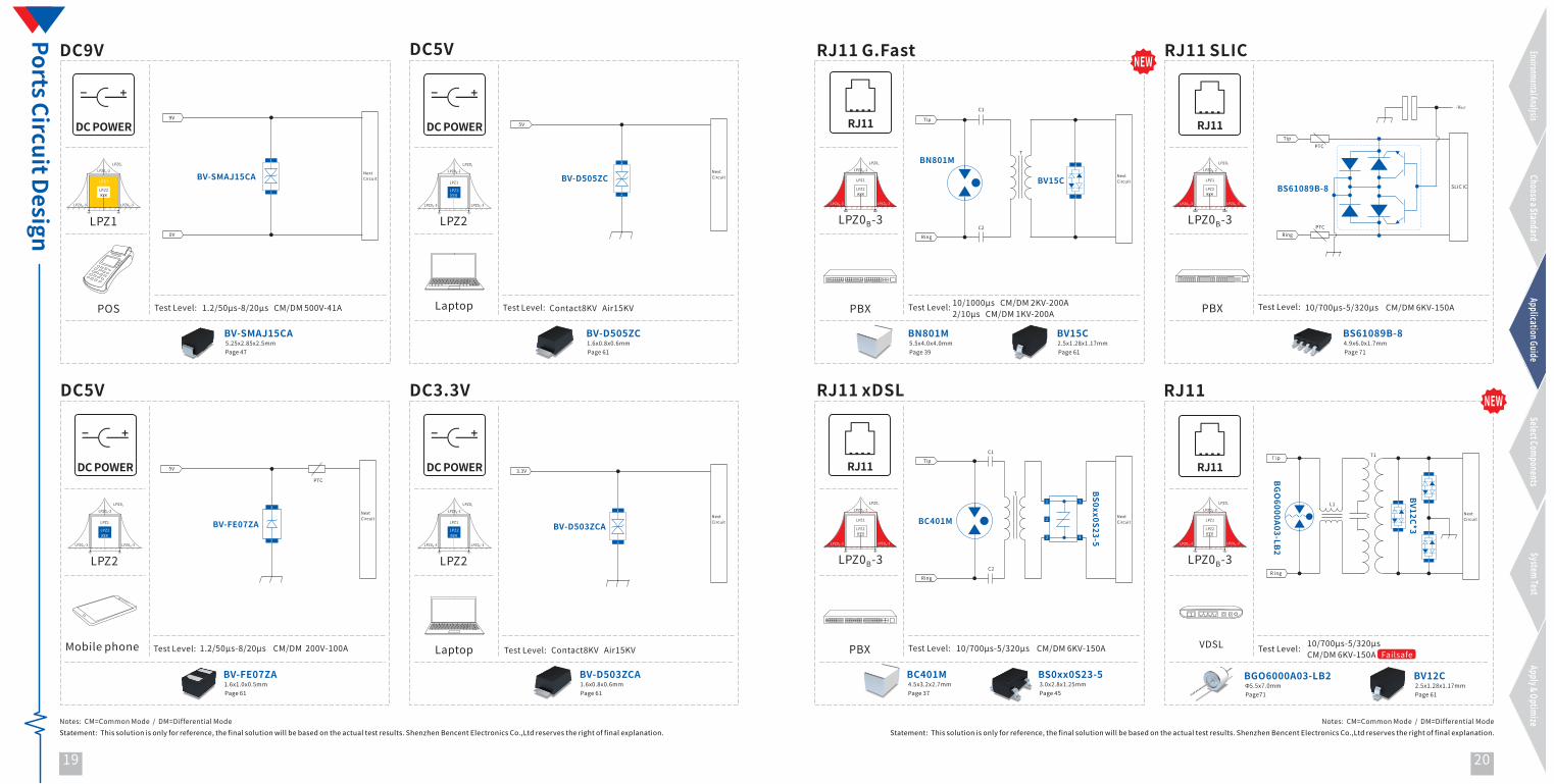
�BS61089B-8
Page�71
Test�Level:
RJ11�SLIC
�10/700μs-5/320μs����CM/DM�6KV-150A
BS61089B-8
TipPTC
RingPTC
-VBAT
SLIC�IC
4.9x6.0x1.7mm
PBX
RJ11
Statement:��This�solution�is�only�for�reference,�the�final�solution�will�be�based�on�the�actual�test�results.�Shenzhen�Bencent�Electronics�Co.,Ltd�reserves�the�right�of�final�explanation.Notes:��CM=Common�Mode��/��DM=Differential�Mode
Statement:��This�solution�is�only�for�reference,�the�final�solution�will�be�based�on�the�actual�test�results.�Shenzhen�Bencent�Electronics�Co.,Ltd�reserves�the�right�of�final�explanation.Notes:��CM=Common�Mode��/��DM=Differential�Mode
19 20
Environmental�AnalysisChoose�a�Standard
Application�GuideSelect�Components
System�TestApply�&�Optimize
Ports�Circuit�Design
�BV-SMAJ15CA5.25x2.85x2.5mmPage�47
Test�Level:
BV-SMAJ15CA
9V
0V
DC9V
1.2/50μs-8/20μs���CM/DM�500V-41APOS
�BV-D505ZC
Page�61
Test�Level: Contact8KV���Air15KV
DC5V
5V
BV-D505ZC
1.6x0.8x0.6mm
Laptop
DC�POWER DC�POWER
1
2
1
2
�BV15C
Page�61
Test�Level:
RJ11�G.Fast
10/1000μs���CM/DM�2KV-200A2/10μs���CM/DM�1KV-200A
RJ11
BN801M
Tip
Ring
C1
C2
T
�BN801M5.5x4.0x4.0mmPage�39
BV15C
2.5x1.28x1.17mm
PBX
1
2
Page�61
Test�Level:
DC3.3V
3.3V
BV-D503ZCA
Contact8KV���Air15KVLaptop
5V
BV-FE07ZA
�BV-FE07ZA
Page�61
Test�Level:
DC5V
1.6x1.0x0.5mm
1.2/50μs-8/20μs����CM/DM��200V-100AMobile�phone�
DC�POWER DC�POWER
1
2
PTC
BV-D503ZCA
1
2
1.6x0.8x0.6mm�BC401M4.5x3.2x2.7mmPage�37
Test�Level:
RJ11�xDSL
10/700μs-5/320μs����CM/DM�6KV-150A
BC401M
Tip
Ring
C1
C2
BS0xx0S23-5
T1
2
3 4
5
�BS0xx0S23-53.0x2.8x1.25mmPage�45
PBX
RJ11
Test�Level:
RJ11
�BV12C2.5x1.28x1.17mmPage�61
T�ip
R�ing
BGO6000A03-LB2
BV12C*3
C
1
2
�BGO6000A03-LB2
Page71Φ5.5x7.0mm
VDSL 10/700μs-5/320μs��CM/DM�6KV-150A���Failsafe
T1
L1
RJ11
1
2
1
2
NextCircuit
NextCircuit Next
Circuit
NextCircuitNext
CircuitNextCircuit
NextCircuit

Statement:��This�solution�is�only�for�reference,�the�final�solution�will�be�based�on�the�actual�test�results.�Shenzhen�Bencent�Electronics�Co.,Ltd�reserves�the�right�of�final�explanation.Notes:��CM=Common�Mode��/��DM=Differential�Mode
Statement:��This�solution�is�only�for�reference,�the�final�solution�will�be�based�on�the�actual�test�results.�Shenzhen�Bencent�Electronics�Co.,Ltd�reserves�the�right�of�final�explanation.Notes:��CM=Common�Mode��/��DM=Differential�Mode
21 22�
Environmental�AnalysisChoose�a�Standard
Application�GuideSelect�Components
System�TestApply�&�Optimize
Ports�Circuit�Design
RJ11
�B3D470L-C
Page�39
Test�Level:
B3D470L-C
Tip
Ring
10/700μs-5/320μs����CM/DM�6KV-150A
7.8x5.0x6.0mm
Portection�Unit
RJ11
4.2x2.7x3.9mmPage�39
Test�Level:
B3A420
TIP
RING
B3A420
BV12C*3
C
L2
L1
10/700μs-5/320μs���6KV-150A
RJ11
PSTN
RJ11
RJ45-100M
�BV-SRV05-4
Page�61
Test�Level: Contact��8KV���Air�15KV
PHY�IC
1
2
3
6
BV-SRV05-4
1 2 3
456
T1
T2
RJ45
R1
R2
R3
R4
2.9x2.8x1.25mm
Switch
RJ11
�BS008023-53.0x2.8x1.25mmPage�45
Test�Level:
BS008023-5
B3Y471M
Tip
Ring
C1
C2
T
�10/700μs-5/320μs���CM/DM�6KV-150A
�B3Y471M6.2x3.2x2.3mmPage�39
PSTN
RJ11
1
2
3 4
5
�BS3100N-C-F
Page�45
Test�Level:
T�ip
RJ11
10/700μs-5/320μs�����CM/DM�6KV-150A
1
2
5.4x3.3x2.0mm
POS
BS3100N-C-F*3
R�ing
RJ11
1
2
1
2
�BS4200N-2C
Page�45
Test�Level:
RJ45-100M
�10/700μs-5/320μs���CM/DM�4KV-100A
C
BS4200N-2CR1 R2
1
2
3
6
PHY�IC
T1
T2
Switch
5.4x3.3x2.0mm
BV03C-H*2
�BV03C-H
Page�612.5x1.28x1.17mm
RJ45
1 3
2
2
2
NextCircuit
NextCircuit
NextCircuit Next
Circuit
�BS4200N-2C/BS0640N-2C5.4x3.3x2.0mmPage�45
Test�Level:
RJ45-1G
C
BS4200N-2CBS0640N-2C
orR1 R2 R3 R4
1
2
3
6
4
5
7
8
PHY�IC
T1
T2
T3
T4
BV03C-H*4
�10/700μs-5/320μs���CM/DM�6KV-330ASwitch
2.2Ω
�BV03C-H
Page�612.5x1.28x1.17mm
RJ45
1 3
2
1 3
2
2
2
2
2
RJ45-1G
BZ801MC
�BZ801M3.2x2.5x2.5mmPage�35
Test�Level: 10/700μs-5/320μs���CM�6KV-150AHi-pot�DC500V
1
23
6PHY�IC
BV03C-H*4
4
57
8
T1
T2
T3
T4
2.2Ω
2.2Ω2.2Ω
2.2Ω2.2Ω
2.2Ω2.2Ω
2.2Ω
�BV03C-H
Page�612.5x1.28x1.17mm
RJ452
2
2
2
LPZ0 -2B
LPZ0A
LPZ2
LPZ1
LPZ0 -2B
LPZ0 -3B LPZ0 -3B
1
21
2 1
2
�BV12C2.5x1.28x1.17mmPage�61
2.2Ω
2.2Ω
2.2Ω
2.2Ω
2.2Ω
2.2Ω
2.2Ω
2.2Ω
2.2Ω
2.2Ω
2.2Ω
Outdoor�AP

Statement:��This�solution�is�only�for�reference,�the�final�solution�will�be�based�on�the�actual�test�results.�Shenzhen�Bencent�Electronics�Co.,Ltd�reserves�the�right�of�final�explanation.Notes:��CM=Common�Mode��/��DM=Differential�Mode
Statement:��This�solution�is�only�for�reference,�the�final�solution�will�be�based�on�the�actual�test�results.�Shenzhen�Bencent�Electronics�Co.,Ltd�reserves�the�right�of�final�explanation.Notes:��CM=Common�Mode��/��DM=Differential�Mode
23 24�
Environmental�AnalysisChoose�a�Standard
Application�GuideSelect�Components
System�TestApply�&�Optimize
Ports�Circuit�Design
�BF091M �BV03CW
Page�37 Page�61
Test�Level:
Video R
C
BF091M
1
2
BV03CW
SDI�
8/20μs���CM�5KA
COAXIAL
2.5x1.28x1.17mm4.2x5.0x5.0mm
Camera
�BS0060N-C-F5.4x3.3x2.0mmPage�43
Test�Level:
BS0060N-C-F
�10/700μs-5/320μs����CM�6KV-150A
Video
VideoChip
1
2
R
CVBS
Camera
COAXIAL
�BV03C-H
Page�61Page�59
Test�Level:
RJ45-1G�PD
BCCSP-58C-654K
BV03C-H*4
R1
C1
R2 R3 R4
C2 C3 C4
C5
1.2/50μs-8/20μs���CM�4KV���DM�2KV
6.5x6.5x0.6mm 2.5x1.28x1.17mm
POE�Switch
213
RJ45
BCCSP-58C-654K
NextCircuit
�BV03C-H�BV-SMCT-58CA8.0x5.9x2.0mm
Page�61Page�59
Test�Level:
RJ45-1G�PD1
23
6
BV-SMCT-58CA
PHY�IC
BV03C-H*4
AC��AC
V+��
V-
2
R1
4
57
8
C1
T1
T2
T3
T4
R2 R3 R4
C2 C3 C4
C5
2.2Ω
2.2Ω2.2Ω
2.2Ω2.2Ω
2.2Ω2.2Ω
2.2Ω
AC��
AC
V+��
V- 1
2
3
�10/700μs-5/320μs���CM/DM�4KV-100A
2.5x1.28x1.17mm
Camera
RJ45
2
2
2
NextCircuit
�BV03C-H
Page�61
Test�Level:
RJ45-1G�PD1
2
3
6
BV-5SMDJ58CA*6
PHY�IC
BV03C-H*4
AC��
AC
V+��
V-
AC��
AC
V+��
V-
4
5
7
8
T1
T2
T3
T4
2.2Ω
2.2Ω
2.2Ω
2.2Ω
2.2Ω
2.2Ω
2.2Ω
2.2Ω
�10/700μs-5/320μs���CM/DM�6KV-150A
2.5x1.28x1.17mm
Outdoor�AP
�BV-5SMDJ58CA
Page�578.25x6.15x2.95mm
RJ45
2
2
2
2
2
1
2
1
2
1
R1
C1
2
1
2
1
2
1
R2 R3 R4
C2 C3 C4
C5
NextCircuit
RJ45-10G
Test�Level:
1
2
BZ401M*4
PHY�IC
C
T1
3
4
7
6
5
8
T2
T3
T4
BV-FE03U2A*4
R*4
�BZ401M3.2x2.5x2.5mmPage�35
�10/700μs-5/320μs���CM�6KV-150A
1.6x1.0x0.55mmPage�61
BV-FE03U2A*4
RJ45
Test�Level:
RJ45-�100M�PD
1
2
4
5
7
BV-SMBJ58C2H*2
PHY�ICBV03CW*2
AC��
AC
V+��
V-
AC V-
2.2Ω
3
6
8
R1
C1
AC��
V+��
1
R2 R3 R4
C2 C3 C4
C5
�10/700μs-5/320μs���CM/DM�4KV-100A
T1
T2
�BV03CW
Page�612.5x1.28x1.17mm
Camera
�BV-SMBJ58C2H
Page�595.45x3.75x2.6mm
RJ45
2
2
2
1
2
1
2.2Ω
2.2Ω
2.2Ω
NextCircuit
�BV03C-H
Page�61Page�37
Test�Level:
RJ45-1G
4.2x5.0x5.0mm 2.5x1.28x1.17mm
POE�Switch
RJ45
BF801MC
1
2
BV03C-H*4
T1
3
6
T2
4
5
T3
7
8
T4
BL091N*4
2
2
2
2
Page�353.2x2.5x2.5mmBL091N BF801M
2.2Ω
2.2Ω
2.2Ω
2.2Ω
2.2Ω
2.2Ω
2.2Ω
2.2Ω
NextCircuit
R
10/700μs-5/320μs���CM/DM�6KV-150AHi-pot�DC500V
1
2
3
6PHY�IC
AC��
AC
V+��
V-
AC��
AC
V+��
V-
4
5
7
8
T1
T2
T3
T4
2.2Ω
2.2Ω
2.2Ω
2.2Ω
2.2Ω
2.2Ω
2.2Ω
2.2Ω
2
2
2
2
NextCircuit
Outdoor�AP
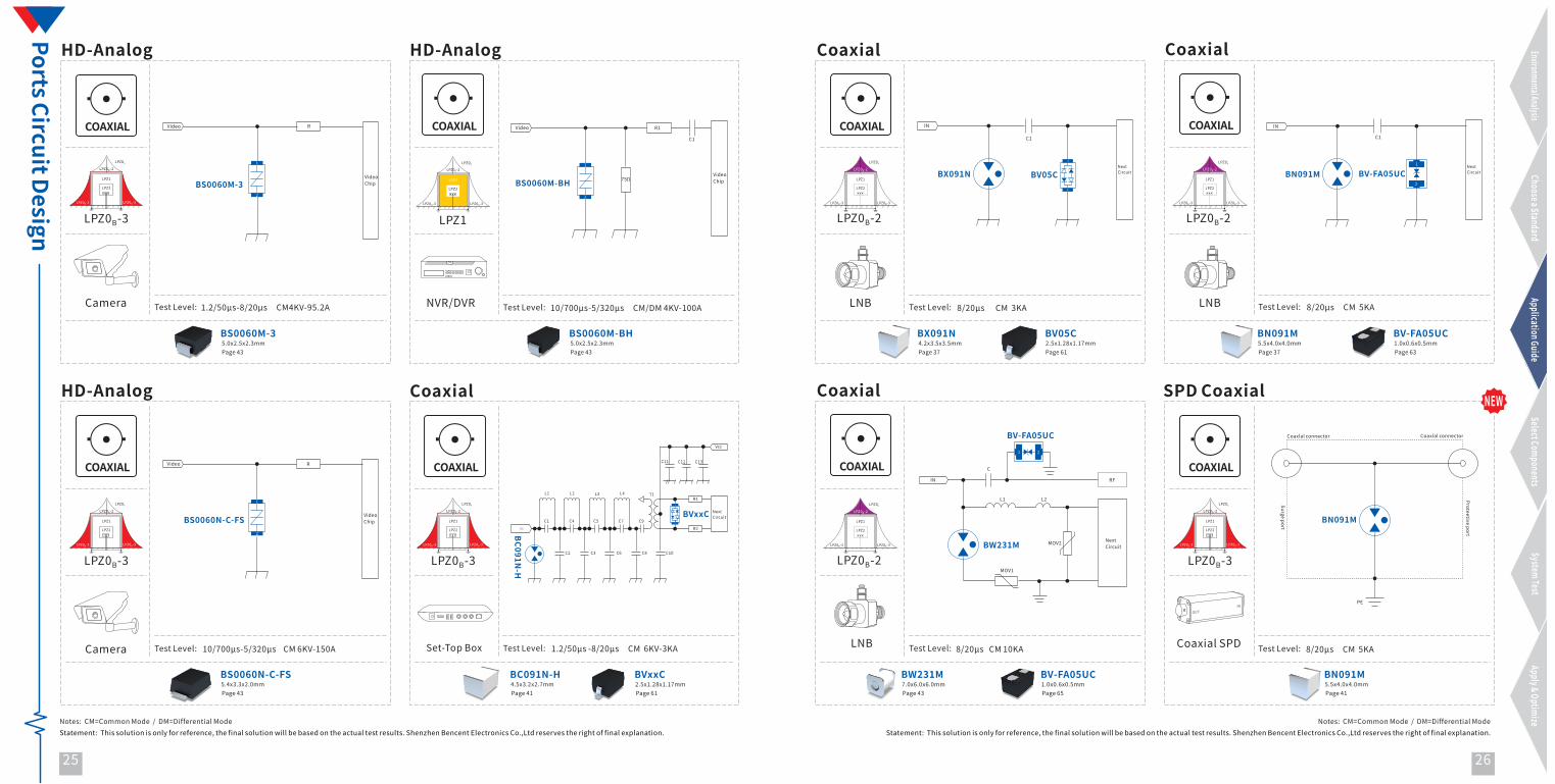
Statement:��This�solution�is�only�for�reference,�the�final�solution�will�be�based�on�the�actual�test�results.�Shenzhen�Bencent�Electronics�Co.,Ltd�reserves�the�right�of�final�explanation.Notes:��CM=Common�Mode��/��DM=Differential�Mode
Statement:��This�solution�is�only�for�reference,�the�final�solution�will�be�based�on�the�actual�test�results.�Shenzhen�Bencent�Electronics�Co.,Ltd�reserves�the�right�of�final�explanation.Notes:��CM=Common�Mode��/��DM=Differential�Mode
25 26�
Environmental�AnalysisChoose�a�Standard
Application�GuideSelect�Components
System�TestApply�&�Optimize
Ports�Circuit�Design
�BS0060M-BH5.0x2.5x2.3mmPage�43
Test�Level: 10/700μs-5/320μs�����CM/DM�4KV-100A
VideoChip
Video R1
75Ω
C1
BS0060M-BH
HD-Analog
NVR/DVR
COAXIAL
1
2
�BS0060N-C-FS
Page�43
Test�Level: 10/700μs-5/320μs����CM�6KV-150A
Video
VideoChip
R
BS0060N-C-FS
HD-Analog
5.4x3.3x2.0mm
Camera
COAXIAL
1
2
�BS0060M-35.0x2.5x2.3mmPage�43
Test�Level:
Video
VideoChipBS0060M-3
R
�1.2/50μs-8/20μs�����CM4KV-95.2A
HD-Analog
Camera
COAXIAL
1
2
Coaxial�
�BC091N-H �BVxxC
Page�41 Page�61
Test�Level: 1.2/50μs�-8/20μs�����CM��6KV-3KA
NextCircuit
L1 L2 L3 L4
C1
C2 C3 C6 C8 C10
C4 C5 C7 C9
T1
BC091N-H
IN
BVxxC
R1
R2
Vcc
1
2
C11 C12 C13
4.5x3.2x2.7mm 2.5x1.28x1.17mm
Set-Top�Box
COAXIAL
�BX091N �BV05C4.2x3.5x3.5mmPage�37 Page�61
Test�Level:
IN
C1
BX091N BV05C
8/20μs������CM��3KA
Coaxial�
2.5x1.28x1.17mm
LNB
COAXIAL
1
2
�BN091M
Page�37
�BV-FA05UC
Page�63
Test�Level: 8/20μs�����CM��5KA
IN
C1
BN091M BV-FA05UC
1.0x0.6x0.5mm5.5x4.0x4.0mm
1
2
LNB
Coaxial�
COAXIAL
�BV-FA05UC
Page�65
Test�Level: 8/20μs���CM�10KA
BW231M
MOV1
L1
C
BV-FA05UC
IN RF
NextCircuit
�BW231M
Page�437.0x6.0x6.0mm
LNB
1.0x0.6x0.5mm
Coaxial�
MOV2
L2
COAXIAL1 2
�BN091M
Page�41
Test�Level:
Coaxlal�connector
Surge�port
Proteetive�port
Coaxlal�connector
PE
BN091M
�8/20μs�����CM��5KA
�SPD�Coaxial
Coaxial�SPD
IN�
OUT
COAXIAL
NextCircuit
NextCircuit
5.5x4.0x4.0mm
LPZ0 -2B
LPZ0A
LPZ2
LPZ1
LPZ0 -2B
LPZ0 -3B LPZ0 -3B
LPZ0 -2B
LPZ0A
LPZ2
LPZ1
LPZ0 -2B
LPZ0 -3B LPZ0 -3B
LPZ0 -2B
LPZ0A
LPZ2
LPZ1
LPZ0 -2B
LPZ0 -3B LPZ0 -3B

Statement:��This�solution�is�only�for�reference,�the�final�solution�will�be�based�on�the�actual�test�results.�Shenzhen�Bencent�Electronics�Co.,Ltd�reserves�the�right�of�final�explanation.Notes:��CM=Common�Mode��/��DM=Differential�Mode
Statement:��This�solution�is�only�for�reference,�the�final�solution�will�be�based�on�the�actual�test�results.�Shenzhen�Bencent�Electronics�Co.,Ltd�reserves�the�right�of�final�explanation.Notes:��CM=Common�Mode��/��DM=Differential�Mode
27 28�
Environmental�AnalysisChoose�a�Standard
Application�GuideSelect�Components
System�TestApply�&�Optimize
Ports�Circuit�Design
�BS0060N-2C
Page�45
Test�Level:
BS0060N-2C
R1
R2
12
3
A�IN
B�IN
10/700μs-5/320μs�����CM/DM�6KV-150A
RS485
5.4x3.3x2.0mm
RS485�Converter
RS485
�BV_SM712
Page�61
Test�Level:
A
B
BV_SM712
Contact8KV����Air15KV
RS485
RS485
2.9x2.4x1.0mm
RS485�Converter
SPD�Coaxial
�BW231M7.0x6.0x6.0mmPage�39
Test�Level:
Coaxlal�connector
Surg
e�po
rt
Proteetive�port
Coaxlal�connector
PE
BW231M
8/20μs������CM��10KACoaxial�SPD
IN�
OUT
COAXIAL
RS485
�BS0060U-2G-18.0x5.9x2.0mmPage�49
Test�Level: 8/20μs����CM/DM�3KA
A�IN
BS0060U-2G-1
R1
R2B�IN
12
3
AISG
RS485
AISG
RS485
�B3D090M-C �BV-SMBT-15CA
Page�39 Page�61
Test�Level:
B3D090M-C
A�in R/PTC
B�in
GND
R/PTC
12
3
BV-SMBT-15CA
8/20μs���CM/DM�3KA
7.8x5.0x6.0mm 5.4x3.3x2.0mm
RS485
�BV-SMBT-15CA
Page�59
Test�Level:
BV-SMBT-15CA
A�in R1
R2B�in
12
3
GND
1.2/50μs-8/20μs����CM/DM�1KV-500A
ALARM
ALARM
5.4x3.3x2.0mm
Camera
�B3D090M-C �BV-SMBT-15CA
Page�39 Page�59
Test�Level:
B3D090M-C
A�in R/PTC
B�in
GND
R/PTC
BV-SMBT-15CA
8/20μs�����CM/DM�3KA
ALARM�
5.4x3.3x2.0mm7.8x5.0x6.0mm
Camera
ALARM
12
3
IO
�BS0300N-2C
Page�45
Test�Level:
BS0300N-2C
R1
R2
A�IN
B�IN
10/700μs-5/320μs����CM/DM�6KV��150A
I/O
5.4x3.3x2.0mm
I/O�module
12
3
NextCircuit
NextCircuit
NextCircuit
NextCircuit
NextCircuit
NextCircuit
NextCircuit
3
1
2
LPZ0 -2B
LPZ0A
LPZ2
LPZ1
LPZ0 -2B
LPZ0 -3B LPZ0 -3B
LPZ0 -2B
LPZ0A
LPZ2
LPZ1
LPZ0 -2B
LPZ0 -3B LPZ0 -3B
LPZ0 -2B
LPZ0A
LPZ2
LPZ1
LPZ0 -2B
LPZ0 -3B LPZ0 -3B

Statement:��This�solution�is�only�for�reference,�the�final�solution�will�be�based�on�the�actual�test�results.�Shenzhen�Bencent�Electronics�Co.,Ltd�reserves�the�right�of�final�explanation.Notes:��CM=Common�Mode��/��DM=Differential�Mode
Statement:��This�solution�is�only�for�reference,�the�final�solution�will�be�based�on�the�actual�test�results.�Shenzhen�Bencent�Electronics�Co.,Ltd�reserves�the�right�of�final�explanation.Notes:��CM=Common�Mode��/��DM=Differential�Mode
29 30
Environmental�AnalysisChoose�a�Standard
Application�GuideSelect�Components
System�TestApply�&�Optimize
Ports�Circuit�Design
Page�61
Test�Level:
BV-D505ZC*3
NextCircuit
R
L
MIC
GND
AUDIO�
Contact8KV�Air15KV
AUDIO
�BV-D505ZC1.6x0.8x0.6mm
1
2
Laptop
1
2
1
2
�BV-SRV05-4
Page�61
Test�Level:
NextCircuit
VPP
CLK
I/O
BV-SRV05-4
VCC
RST
SIM
SIM
Contact8KV���Air15KV
2.9x2.8x1.25mm
Mobile�phone�
�BV-SRV05-42.9x2.8x1.25mmPage�61
Test�Level:
BV-SRV05-4*2
CD/DAT3
CMD
VCC
CLK
DAT0
DAT1
DAT2
SD
�Contact8KV�Air15KV
�MICO�SD
Mobile�phone�
456
1 2 3
456
1 2 3
456
1 2 3
Page�65
Test�Level:
CAN�BUS
Contact8KV���Air15KV
CAN
2.9x2.4x1.0mm
Vehicle
�BV-D505ZC1.6x0.8x0.6mmPage�61
Test�Level:
VIN�� RESET
GND
VCCVCC
C
1
2
BV-D505ZC
BV-D505ZC
Speaker�Headphone��and�Reset�
Contact8KV����Air15KV
Headphone�
Mobile�phone�
H
L
BV-T324Z2CA
BV-T324Z2CA
1
2
NextCircuit
NextCircuit
NextCircuit 3
1
2
Page�61
Test�Level:
1
2
3
4
5
6
7
8
9�
10�
11�
12�
13�
14�
15�
16�
17�
18�
19
TX2+TX2_SHIELD
TX2-
Tx1+
TX1_SHIELDTX1-
TX0+
TX0_SHIELD
TX0-TXC+
TXC_SHIELD
TXC-
CEC-
N.C
SCL
SDA
GNDHPD
SVDC
TX2+
TX2-
Tx1+
TX1-
TX0+
TX0-
TXC+
TXC-
CEC-SCL
SDA
HPD
SVDC
HDMI�connector
BV-SRV05-4
BV-FK05U4CA*2
HDMI
Contact8KV�Air15KV
HDMI
�BV-SRV05-4
Page�612.5x1.0x0.58mm 2.9x2.8x1.25mm
Laptop
1
2
3
4
5 6
7
8
9
10
1
2
3
4
5 6
7
8
9
10
456
1 2 3
BV-FK05U4CA*2
�BV-D505ZC
Page�61
Test�Level:
VCC
BV-D505ZC NextCircuit
R
1
2
KEY
Contact8KV�Air15KV
KEY
1.6x0.8x0.6mm
Navigator Test�Level: Contact8KV��Air15KV
Page�691.6x0.8x0.6mmBVF-D505ZA
Vehicle
VCC
R
2
1
KEY
BVF-D505ZA
KEY
NextCircuit
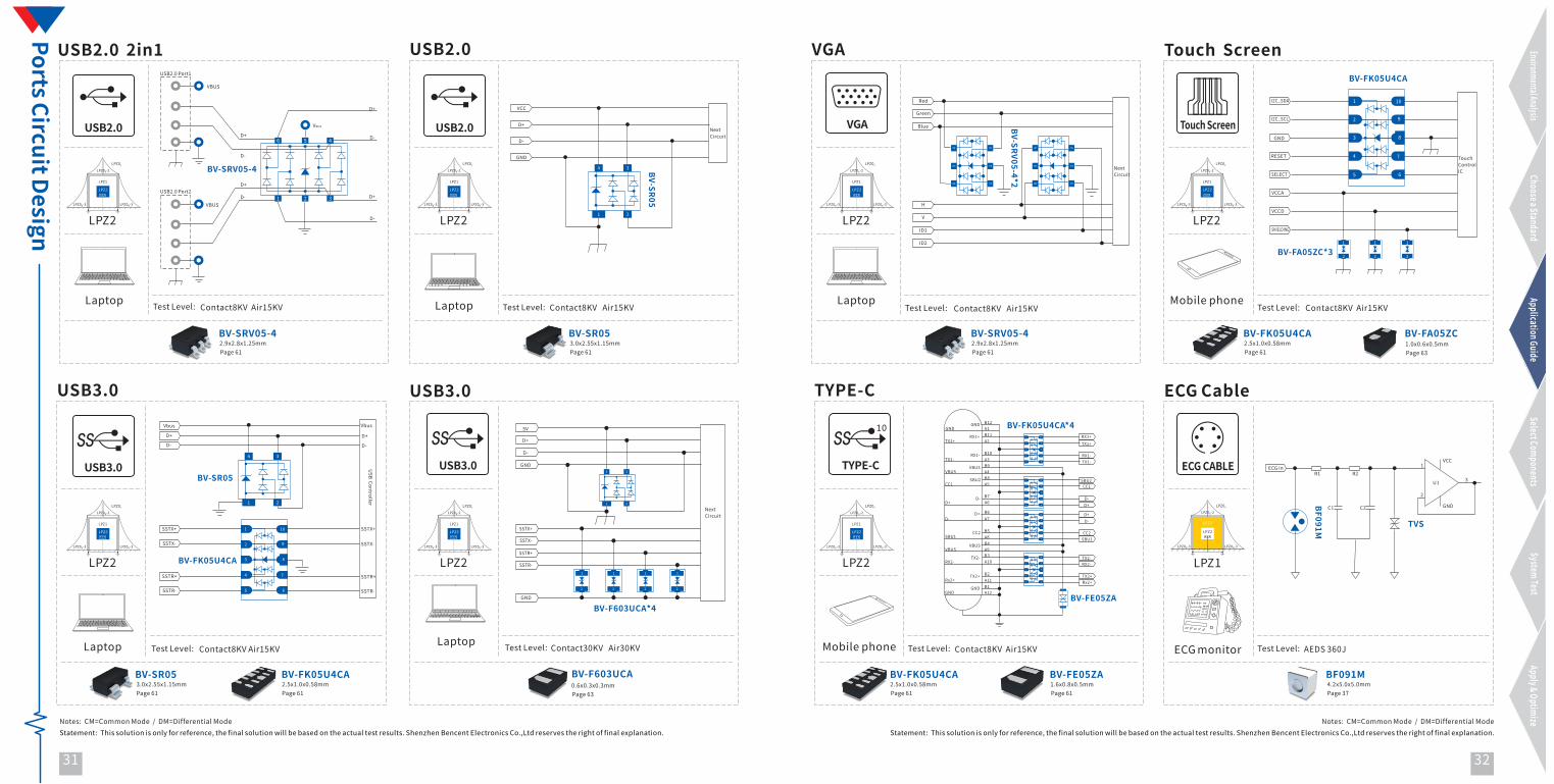
Statement:��This�solution�is�only�for�reference,�the�final�solution�will�be�based�on�the�actual�test�results.�Shenzhen�Bencent�Electronics�Co.,Ltd�reserves�the�right�of�final�explanation.Notes:��CM=Common�Mode��/��DM=Differential�Mode
Statement:��This�solution�is�only�for�reference,�the�final�solution�will�be�based�on�the�actual�test�results.�Shenzhen�Bencent�Electronics�Co.,Ltd�reserves�the�right�of�final�explanation.Notes:��CM=Common�Mode��/��DM=Differential�Mode
31 32�
Environmental�AnalysisChoose�a�Standard
Application�GuideSelect�Components
System�TestApply�&�Optimize
Ports�Circuit�Design
�BV-SRV05-4
Page�61
Test�Level:
BV-SRV05-4
USB2.0�Port1
USB2.0�Port2
D+
D-
D+
D-
D+
D-
D+
D-
VBUS
VBUS
VBUS
1 2 3
456
USB2.0��2in1�
Contact8KV��Air15KV
USB2.0
2.9x2.8x1.25mm
Laptop
�BV-SR053.0x2.55x1.15mmPage�61
Test�Level:
NextCircuit
BV-SR05
VCC
D+
D-
GND
1 2
34
USB2.0�
Contact8KV���Air15KVLaptop
USB2.0
USB3.0�
Test�Level:
D+
D-
Vbus
SSTX+
SSTX-
SSTR+
SSTR-
D+
D-
SSTX+
SSTX-
SSTR+
SSTR-
USB��Controller
Vbus
Contact8KV�Air15KV
USB3.0
2.5x1.0x0.58mmPage�61
BV-SR05
1 2
34
�BV-SR053.0x2.55x1.15mmPage�61
Laptop
Page�63
Test�Level:
USB3.0
0.6x0.3x0.3mm
Laptop
BV-F603UCA
BV-F603UCA*4
NextCircuit
5V
D+
D-
GND
GND
SSTX+
SSTX-
SSTR+
SSTR-
USB3.0
Contact30KV���Air30KV
BV-FK05U4CA
BV-FK05U4CA
�BV-SRV05-4
Page�61
Test�Level:
BV-SRV05-4*2
Red
Green
Blue
ID1
V
ID2
H
NextCircuit
45
6 12
3
VGA�
Contact8KV���Air15KV
VGA
2.9x2.8x1.25mm
Laptop
Page�61
Test�Level:
Touch�Screen
Contact8KV��Air15KV
Touch�Screen
2.5x1.0x0.58mm
Mobile�phone�
TouchControlIC
SHIELDING
VCCA
VCCD
1
2
I2C_SDA
I2C_SCL
GND
RESET
SELECT
BV-FA05ZC*3
�BV-FA05ZC
Page�631.0x0.6x0.5mm
BV-FK05U4CA
BV-FK05U4CA
1
2
3
4
5 6
7
8
9
10
1
2
1
2
45
6 12
3
�BF091M4.2x5.0x5.0mmPage�37
Test�Level:
ECG�inVCC
GND
U1 3
2
1R1 R2
C1 C2
BF091M TVS
ECG�Cable
ECG�CABLE
AEDS�360J
80
98 69
33 21
121 81
97 65
ECG�monitor
�BV-FE05ZA
Page�61 Page�61
Test�Level: Contact8KV��Air15KV
GND
RX1+TX1+
RX1-TX1-
VBUSVBUS
SBU2CC1
D-D+
D+D-
CC2SBU1
VBUSVBUS
TX2-RX2-
TX2+Rx2+
GNDGND
B12A1B11A2
B10A3B9A4B8A5
B7A6
B6A7
B5A8B4A9B3A10
B2A11B1A12
BV-FE05ZA
RX1+TX1+
RX1-TX1-
SBU2CC1
D-D+
D+D-
CC2SBU1
TX2-RX2-
TX2+Rx2+
GND
TYPE-C
TYPE-C
2.5x1.0x0.58mm 1.6x0.8x0.5mm
1
2
Mobile�phone�
BV-FK05U4CA*4
BV-FK05U4CA
1
2
3
4
5 6
7
8
9
10
1
2
3
4
5 6
7
8
9
10
1
2
3
4
5 6
7
8
9
10
1
2
3
4
5 6
7
8
9
10
1
2
3
4
5 6
7
8
9
10
1
2
1
2
1
2
1
2
1 2
34
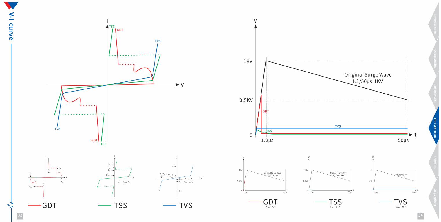
V
GDT�� TSS
I
1KV
01.2μs 50μs
0.5KV
TVS�� GDT�� TSS TVS��
ITISIH
V
I
VBR
VGlow
VAVBR
VGlow
IDRM
VDRM
V
VT VS
V
IPP
VC VBR VDRM IRIDRM
IDRMIR VDRM VBR VC
IPP
1KV
01.2μs 50μs
0.5KV
1KV 1KV
0 01.2μs 1.2μs50μs 50μs
0.5KV 0.5KV
V
t
V
t t t
VA
Original�Surge�Wave�������1.2/50μs��1KV
Original�Surge�Wave�������1.2/50μs��1KV
Original�Surge�Wave�������1.2/50μs��1KV
Original�Surge�Wave�������1.2/50μs��1KV
V =90VDRM V =58VDRM V =58VDRM
V VI I
GDT
TVS
TSS
TVS
GDTTSS
TSSTVS
GDT
V-I��curve
33 34
Environmental�AnalysisChoose�a�Standard
Application�GuideSelect�Components
System�TestApply�&�Optimize

DC�BreakdownVoltage(V )BR
100V/s(V)
Impulse�DischargeCurrent8/20μs(KA)
Part�Number
Tolerance
of��VBR(V)
Impulse�Spark-overVoltage1KV/μs(V)
Arc�Voltage
(V )a(V)@1A
InsulationResistance���(GΩ)
CapacitanceCo(pF)
0.5VDC@1MHzApplication Circuit Outline@DC
(V)
SizeL*W*H(mm)
Remarks
UL497B UL1449 New�products
BS201N
BS401N
BZ091N
BZ201M
BZ301M
BZ401M
BA151N
BA201N
BA301N
BA301N-D
BA401N-D
BA601N
BC091N
200
400
90
200
300
400
150
200
300
300
400
600
90
140-260
280-520
63-117
160-240
240-360
360-580
105-195
140-260
210-390
210-390
340-550
420-780
63-117
≤850
≤1100
≤700
≤800
≤850
≤950
≤750
≤750
≤800
≤750
≤750
≤1200
≤650
〜10
〜8
〜8
〜8
〜8
〜10
〜8
〜8
〜8
〜15
〜15
〜15
〜8
0.5
0.5
1
1
1
1
1
1
1
1
1
1
2
≥1
≥1
≥1
≥1
≥1
≥1
≥1
≥1
≥1
≥1
≥1
≥1
≥1
100
100
50
100
100
100
50
100
100
100
100
100
50
≤0.6
≤0.6
≤0.5
≤0.5
≤0.5
≤1.0
≤1
≤1
≤1
≤1
≤1
≤1
≤1
3.2x1.6x1.6
3.2x1.6x1.6
3.2x2.5x2.5
3.2x2.5x2.5
3.2x2.5x2.5
3.2x2.5x2.5
4.5x3.2x2.7
4.5x3.2x2.7
4.5x3.2x2.7
4.5x3.2x2.7
4.5x3.2x2.7
4.5x3.2x2.7
4.5x3.2x2.7
Ethernet
Ethernet
Coaxial/Internet
RJ11/RJ45
RS485/232/422
Ethernet
RS485/232/422
RS485/232/422
DC12V/AC24V
xDSL
Ethernet
Coaxial
Datasheet�/�GDT
35 36
Coaxial
Environmental�AnalysisChoose�a�Standard
Application�GuideSelect�Components
System�TestApply�&�Optimize
BG075N
BG091N
BG151N
BG201N
BG301N
BG401N
BG601M
BG801M
BG102M
BL075N
BL091N
BL151N
BL201N
BL301N
BL401N
BL601M
BL801M
BL102M
75
90
150
200
300
400
600
800
1000
75
90
150
200
300
400
600
800
1000
53-977
63-117
105-195
140-260
210-390
280-520
480-720
640-960
800-1200
53-977
63-117
105-195
140-260
210-390
280-520
480-720
640-960
800-1200
≤650
≤650
≤700
≤750
≤850
≤1000
≤1200
≤1300
≤1500
≤650
≤650
≤700
≤750
≤850
≤1000
≤1200
≤1300
≤1500
〜8
〜10
〜10
〜10
〜10
〜10
〜10
〜10
〜10
〜8
〜10
〜10
〜10
〜10
〜10
〜10
〜10
〜10
1
1
1
1
1
1
0.5
0.5
0.5
1
1
1
1
1
1
0.5
0.5
0.5
≥1
≥1
≥1
≥1
≥1
≥1
≥1
≥1
≥1
≥1
≥1
≥1
≥1
≥1
≥1
≥1
≥1
≥1
25
50
50
100
100
100
100
100
100
25
50
50
100
100
100
100
100
100
≤0.5
≤0.5
≤0.5
≤0.5
≤0.5
≤0.5
≤0.5
≤0.5
≤0.5
≤0.5
≤0.5
≤0.5
≤0.5
≤0.5
≤0.5
≤0.5
≤0.5
≤0.5
2.9x2.1x1.9
2.9x2.1x1.9
2.9x2.1x1.9
2.9x2.1x1.9
2.9x2.1x1.9
2.9x2.1x1.9
2.9x2.1x1.9
2.9x2.1x1.9
2.9x2.1x1.9
2.9x2.1x1.9
2.9x2.1x1.9
2.9x2.1x1.9
2.9x2.1x1.9
2.9x2.1x1.9
2.9x2.1x1.9
2.9x2.1x1.9
2.9x2.1x1.9
2.9x2.1x1.9
RS485/232/422
RS485/232/422
RS485/232/422
RS485/232/422
RS485/232/422
RS485/232/422
RS485/232/422
RS485/232/422
RS485/232/422
RS485/232/422
RS485/232/422
RS485/232/422
RS485/232/422
RS485/232/422
RS485/232/422
RS485/232/422
RS485/232/422
RS485/232/422
BZ801M 800 640-960 ≤1300 〜10 1 ≥1 100 ≤1.0 3.2x2.5x2.5 Ethernet
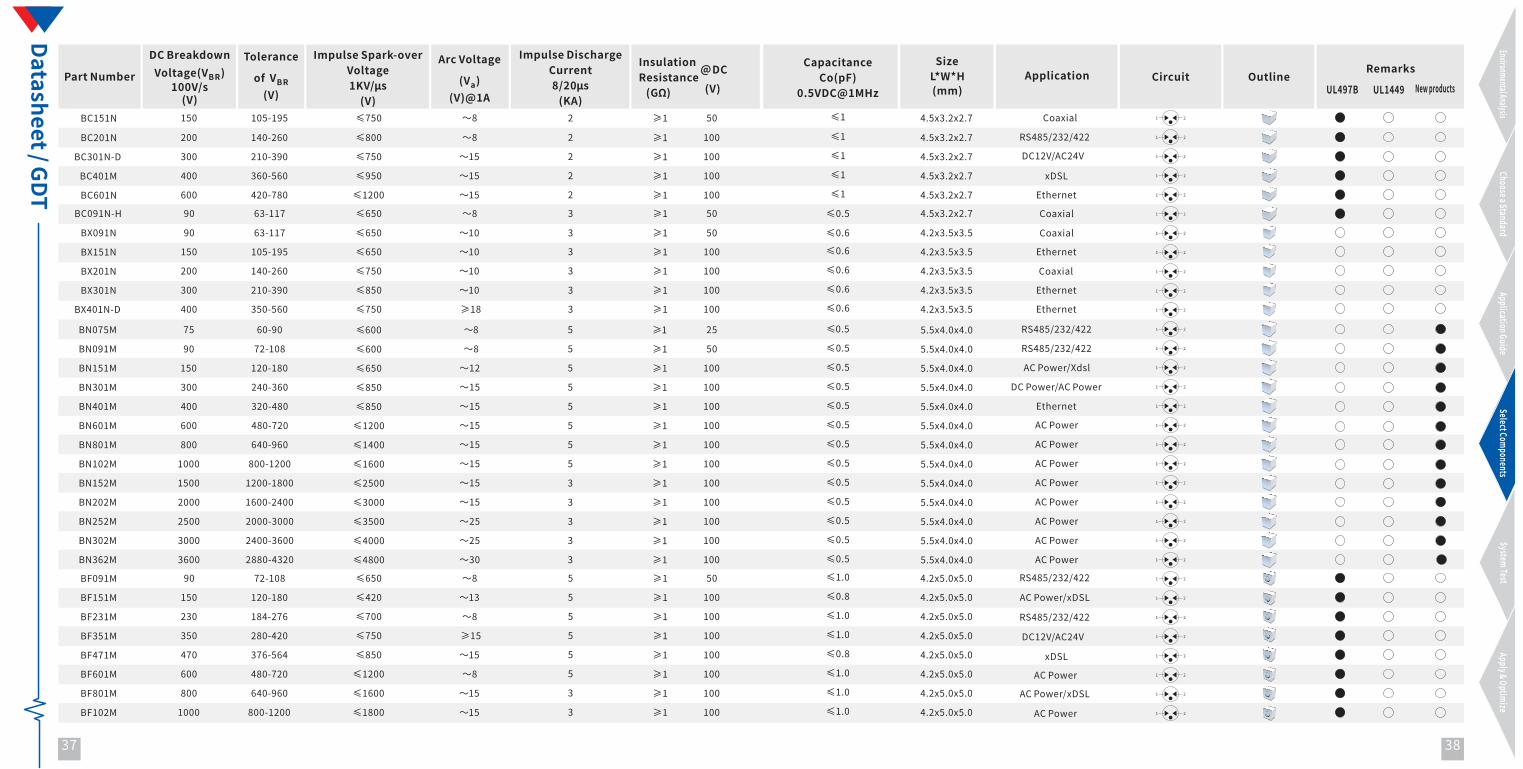
37 38
Environmental�AnalysisChoose�a�Standard
Application�GuideSelect�Components
System�TestApply�&�Optimize
Datasheet�/�GDT
BC201N
BC301N-D
BC401M
BC601N
BX091N
BX151N
BX201N
BX301N
200
300
400
600
90
150
200
300
140-260
210-390
360-560
420-780
63-117
105-195
140-260
210-390
≤800
≤750
≤950
≤1200
≤650
≤650
≤750
≤850
〜8
〜15
〜15
〜15
〜10
〜10
〜10
〜10
2
2
2
2
3
3
3
3
≥1
≥1
≥1
≥1
≥1
≥1
≥1
≥1
100
100
100
100
50
100
100
100
≤1
≤1
≤1
≤1
≤0.6
≤0.6
≤0.6
≤0.6
4.5x3.2x2.7
4.5x3.2x2.7
4.5x3.2x2.7
4.5x3.2x2.7
4.2x3.5x3.5
4.2x3.5x3.5
4.2x3.5x3.5
4.2x3.5x3.5
RS485/232/422
DC12V/AC24V
xDSL
Ethernet
Coaxial
�Coaxial
Ethernet
Ethernet
BX401N-D 400 350-560 ≤750 3 ≥1 100 ≤0.6 4.2x3.5x3.5 Ethernet≥18
BC091N-H 90 63-117 ≤650 〜8 3 ≥1 50 ≤0.5 4.5x3.2x2.7 Coaxial
BF091M
BF151M
BF231M
BF351M
BF471M
BF601M
BF801M
BF102M
90
150
230
350
470
600
800
1000
72-108
120-180
184-276
280-420
376-564
480-720
640-960
800-1200
≤650
≤420
≤700
≤750
≤850
≤1200
≤1600
≤1800
〜8
〜13
〜8
≥15
〜15
〜8
〜15
〜15
5
5
5
5
5
5
3
3
≥1
≥1
≥1
≥1
≥1
≥1
≥1
≥1
50
100
100
100
100
100
100
100
≤1.0
≤0.8
≤1.0
≤1.0
≤0.8
≤1.0
≤1.0
≤1.0
4.2x5.0x5.0
4.2x5.0x5.0
4.2x5.0x5.0
4.2x5.0x5.0
4.2x5.0x5.0
4.2x5.0x5.0
4.2x5.0x5.0
4.2x5.0x5.0
RS485/232/422
AC�Power/xDSL
RS485/232/422
DC12V/AC24V
xDSL
AC�Power
AC�Power/xDSL
AC�Power
BN075M
BN091M
BN151M
BN301M
BN401M
BN601M
BN801M
BN102M
BN152M
BN202M
BN252M
BN302M
BN362M
75
90
150
300
400
600
800
1000
1500
2000
2500
3000
3600
60-90
72-108
120-180
240-360
320-480
480-720
640-960
800-1200
1200-1800
1600-2400
2000-3000
2400-3600
2880-4320
�≤600
�≤600
≤650
≤850
≤850
≤1200
≤1400
≤1600
≤2500
≤3000
≤3500
≤4000
≤4800
〜8
〜8
〜12
〜15
〜15
〜15
〜15
〜15
〜15
〜15
〜25
〜25
〜30
5
5
5
5
5
5
5
5
3
3
3
3
3
≥1
≥1
≥1
≥1
≥1
≥1
≥1
≥1
≥1
≥1
≥1
≥1
≥1
�25
�50
�100
�100
�100
�100
�100
�100
�100
�100
�100
�100
�100
≤0.5
≤0.5
≤0.5
≤0.5
≤0.5
≤0.5
≤0.5
≤0.5
≤0.5
≤0.5
≤0.5
≤0.5
≤0.5
5.5x4.0x4.0
5.5x4.0x4.0
5.5x4.0x4.0
5.5x4.0x4.0
5.5x4.0x4.0
5.5x4.0x4.0
5.5x4.0x4.0
5.5x4.0x4.0
5.5x4.0x4.0
5.5x4.0x4.0
5.5x4.0x4.0
5.5x4.0x4.0
5.5x4.0x4.0
RS485/232/422
RS485/232/422
AC�Power/Xdsl
DC�Power/AC�Power
Ethernet
AC�Power
AC�Power
AC�Power
AC�Power
AC�Power
AC�Power
AC�Power
AC�Power
DC�BreakdownVoltage(V )BR
100V/s(V)
Impulse�DischargeCurrent8/20μs(KA)
Part�Number
Tolerance
of��VBR(V)
Impulse�Spark-overVoltage1KV/μs(V)
Arc�Voltage
(V )a(V)@1A
InsulationResistance���(GΩ)
CapacitanceCo(pF)
0.5VDC@1MHzApplication Circuit Outline@DC
(V)
SizeL*W*H(mm)
Remarks
UL497B UL1449 New�products
BC151N 150 105-195 ≤750 〜8 2 ≥1 50 ≤1 4.5x3.2x2.7 Coaxial
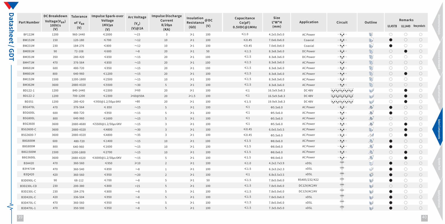
BM351M
BM471M
BM601M
BM801M
BM152M
BM362M
BD122-1
B5G470L
B5G600L
B5G800L
B5G3600
B8G600M
B8G800M
B8G1500M
B8G3600L
B3Y471M
B3Q420
B3D090L-C
B3D230L-CD
350
470
600
�800
1500
3600
1200
470
600
800
3600
�600
800
1500
3600
470
420
90
230
280-420
376-564
480-720
640-960
1200-1800
2880-4320
840-1440�
376-564
480-720
640-960
2880-4680
�480-720
�640-960
�1200-1800
�2880-4320
360-540
360-560
68-112
200-380
≤650
≤850
≤950
≤1200
≤2500
≤5500
≤2300
≤�850
≤950
≤1600
≤[email protected]/50μs�6KV
≤1400
�≤1600
�≤2700
�≤[email protected]/50μs�6KV
≤850
≤950
≤700
≤800
〜15
〜15
〜15
〜15
〜15
〜30
�≥60
〜15
〜15
〜15
〜15
〜15
〜15
〜15
〜15
〜8
〜20
〜8
>15
20
20
20
20
10
5
5
5
5
3
10
10
10
5
1
2
5
5
≥1
≥1
≥1
≥1�
≥1�
≥1�
�≥1
≥1
≥1
≥1
≥1
≥1
≥1
≥1
≥1
≥1
≥1
≥1
≥1
�100
�100
�100
100
100
100
100
100
100
100
100
�100
100
100
100
100
100
50
100
≤1.5
≤1.5
≤1.5
≤1.5
≤1.5
≤1.5
�≤1
≤1
≤1
≤1
≤1
�≤1.5
�≤1.5
�≤1.5
�≤1.5
≤1.5
≤1
≤1.5
≤1.5
8.3x8.3x6.0
8.3x8.3x6.0
8.3x8.3x6.0
8.3x8.3x6.0
8.3x8.3x6.0
8.3x8.3x6.0
Φ5.5x6.0
Φ5.5x6.0
Φ5.5x6.0
Φ5.5x6.0
Φ8.0x6.0
Φ8.0x6.0
Φ8.0x6.0
Φ8.0x6.0
6.2x3.2x2.3
6.8x3.5x3.5
7.8x5.0x6.0
7.8x5.0x6.0
DC�Power
AC�Power
AC�Power
AC�Power
AC�Power
DC�48V
AC�Power
AC�Power
AC�Power
AC�Power
AC�Power
AC�Power
AC�Power
AC�Power
xDSL
xDSL
RS485/232/422
DC12V/AC24V
B3D420L-C
B3D470L-C
420
470
336-504
360-560
≤950
≤950
〜8
〜8
5
5
≥1
≥1
100
100
≤1.5
≤1.5
7.8x5.0x6.0
7.8x5.0x6.0
xDSL
xDSL
BM091M� 90 72-108 �≤600 〜8 20 ≥1 �50 ≤1.5 8.3x8.3x6.0 DC�Power
B3D230L-C
20
230 184-276 ≤800 5 ≥1 100 ≤1.5 7.8x5.0x6.0 DC12V/AC24V〜8
AC�Power
39 40
BW231M 230 184-276 ≤800 〜12 10 ≥1 100 ≤0.45 7.0x6.0x6.0 Coaxial
BW151M 150 120-180 ≤700 〜12 10 ≥1 100 ≤0.45 7.0x6.0x6.0 Coaxial
BD122-2 1200 700-1200� ≤2300 �≥60@50A �≥1.5� 100 �≤1 16.5x9.5x8.3 DC�48V20
BD351 1200 280-420� ≤[email protected]/50μs�6KV �>80 �≥1 100 �≤1.5 19.9x9.3x8.3 DC�48V20
16.5x9.5x8.3
B3D470L-1 470 350-500 ≤950 〜8 5 ≥1 100 ≤1.5 7.3x5.0x5.0 xDSL
B3A420 470 360-560 ≤950 2 ≥1 100 ≤1.0 4.2x2.7x3.9≥10 xDSL
B5G3600-C 3600 2880-4320 ≤4800 〜30 3 ≥1 100 ≤0.45 6.0x5.5x5.5 AC�Power
Environmental�AnalysisChoose�a�Standard
Application�GuideSelect�Components
System�TestApply�&�Optimize
Datasheet�/�GDT
DC�BreakdownVoltage(V )BR
100V/s(V)
Impulse�DischargeCurrent8/20μs(KA)
Part�Number
Tolerance
of��VBR(V)
Impulse�Spark-overVoltage1KV/μs(V)
Arc�Voltage
(V )a(V)@1A
InsulationResistance���(GΩ)
CapacitanceCo(pF)
0.5VDC@1MHzApplication Circuit Outline@DC
(V)
SizeL*W*H(mm)
Remarks
UL497B UL1449 New�products
BF122M 1200 960-1440 ≤2000 〜15 3 ≥1 100 ≤1.0 4.2x5.0x5.0 AC�Power
B5G3600-7 3600 2880-4320 ≤4800 〜35 3 ≥1 100 ≤0.45 AC�PowerΦ5.5x6.0
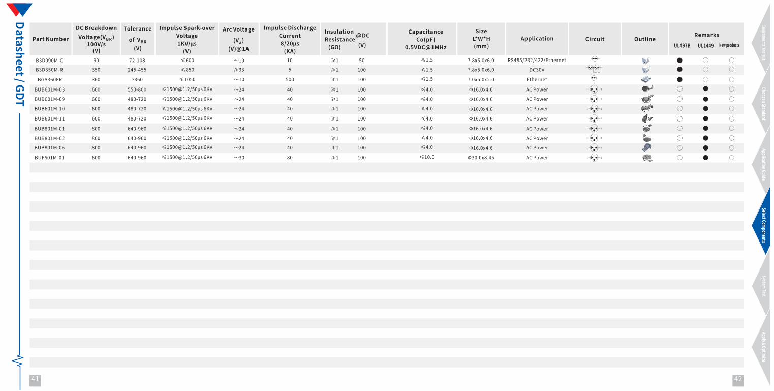
41 42
BUB601M-03
BUB801M-01
BUB801M-02
600
800
800
550-800
640-960
640-960
〜24
〜24
〜24
40
40
40
≥1
≥1
≥1
100
100
100
≤4.0
≤4.0
≤4.0
Φ16.0x4.6 AC�Power
AC�Power
AC�Power
BUB801M-06 800 640-960 〜24 40 ≥1 100 ≤4.0 AC�Power
≤[email protected]/50μs�6KV
≤[email protected]/50μs�6KV
≤[email protected]/50μs�6KV
BUB601M-09 600 480-720 〜24 40 ≥1 100 ≤4.0 AC�Power
BUB601M-10 600 480-720 〜24 40 ≥1 100 ≤4.0 AC�Power
BUF601M-01 600 640-960 〜30 80 ≥1 100 ≤10.0 Φ30.0x8.45 AC�Power≤[email protected]/50μs�6KV
BUB601M-11 600 ≤[email protected]/50μs�6KV 〜24 40 ≥1 100 ≤4.0 AC�Power480-720
Φ16.0x4.6
Φ16.0x4.6
Φ16.0x4.6
Φ16.0x4.6
Φ16.0x4.6
Φ16.0x4.6
≤[email protected]/50μs�6KV
≤[email protected]/50μs�6KV
≤[email protected]/50μs�6KV
BGA360FR 360 ≤1050 500 ≥1 100 ≤1.5 7.0x5.0x2.0>360 Ethernet〜10
Environmental�AnalysisChoose�a�Standard
Application�GuideSelect�Components
System�TestApply�&�Optimize
Datasheet�/�GDT
DC�BreakdownVoltage(V )BR
100V/s(V)
Impulse�DischargeCurrent8/20μs(KA)
Part�Number
Tolerance
of��VBR(V)
Impulse�Spark-overVoltage1KV/μs(V)
Arc�Voltage
(V )a(V)@1A
InsulationResistance���(GΩ)
CapacitanceCo(pF)
0.5VDC@1MHzApplication Circuit Outline@DC
(V)
SizeL*W*H(mm)
Remarks
UL497B UL1449 New�products
B3D350M-R 350 245-455 ≤850 ≥33 5 ≥1 100 ≤1.5 7.8x5.0x6.0 DC30V
B3D090M-C 90 72-108 ≤600 〜10 10 ≥1 50 ≤1.5 7.8x5.0x6.0 RS485/232/422/Ethernet
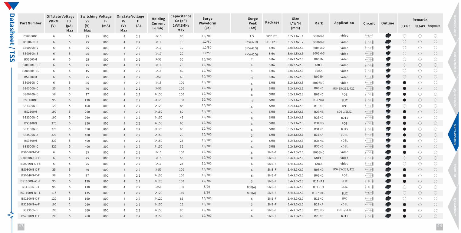
Part�NumberHolding�Current�IH(mA)
CapacitanceCo�(pF)
2V@1MHZ
Max
SurgeWaveform
(μs)
Surge�Peak(KV)
SizeL*W*H(mm)
Mark Application Circuit OutlinePackageRemarks
UL497B UL1449 New�products
BS0060D1
BS0060D-2
BS0060M-2
BS0060M-3
BS0060M
BS0080M
6
6
6
6
6
6
5
5
5
5
5
5
25
25
25
25
25
25
800
800
800
800
800
800
4
4
4
4
4
4
2.2
2.2
2.2
2.2
2.2
2.2
≥15
≥10
≥10
≥10
≥50
≥50
80
10
10
20
50
60
10/700
1.2/50
1.2/50
1.2/50
10/700
10/700
1.5
3KV(42Ω)
3KV(42Ω)
4KV(42Ω)2
3
SOD123
SOD123F
SMA
SMA
SMA
SMA
3.7x1.6x1.1
3.7x1.8x1.2
5.0x2.5x2.3
5.0x2.5x2.3
5.0x2.5x2.3
5.0x2.5x2.3
B006D-2
B006M-2
B006M-3
B006M
B008M
video
video
video
video
video
BS0060N-C
BS0300N-C
BS0640N-C
BS1100N1
BS1300N-C
BS2300N
BS2300N-C
BS3100N
BS3100N-C
BS3500N-A
BS3500N
BS3500N-C
BS0060N-C-F
BS0060N-C-FLC
BS0060N-C-FS
BS0300N-C-F
BS0640N-C-F
BS1100N-A1-F
BS1100N-D1
BS1100N-D1-L
BS1300N-C-F
BS2300N-A-F
BS2300N-F
BS2300N-C-F
6
25
58
95
120
190
190
275
275
320
320
320
6
6
6
25
58
95
95
115
120
190
190
190
5
5
5
5
5
5
5
5
5
5
5
5
5
5
5
5
5
5
5
5
5
1
5
5
25
40
77
130
160
260
260
350
350
400
400
400
25
25
25
40
77
130
130
135
160
260
260
260
800
800
800
800
800
800
800
800
800
800
800
800
800
800
800
800
800
800
800
800
800
800
800
800
4
4
4
4
4
4
4
4
4
4
4
4
4
4
4
4
4
4
4
4
4
4
4
4
2.2
2.2
2.2
2.2
2.2
2.2
2.2
2.2
2.2
2.2
2.2
2.2
2.2
2.2
2.2
2.2
2.2
2.2
2.2
2.2
2.2
2.2
2.2
2.2
≥15
≥50
≥150
≥120
≥120
≥150
≥150
≥150
≥120
≥150
≥150
≥150
≥15
≥15
≥10
≥50
≥150
≥120
≥50
≥120
≥120
≥150
≥150
≥150
100
100
100
150
85
80
45
60
80
20
25
35
100
55
25
100
100
100
150
160
85
25
80
45
10/700
10/700
10/700
10/700
10/700
10/700
10/700
10/700
10/700
10/700
10/700
10/700
10/700
10/700
10/700
10/700
10/700
10/700
8/20
8/20
10/700
10/700
10/700
10/700
6
6
6
3
6
4
6
4
6
3
4
6
6
6
6
6
6
3
800(A)
800(A)
6
3
4
6
SMB
SMB
SMB
SMB
SMB
SMB
SMB
SMB
SMB
SMB
SMB
SMB
SMB-F
SMB-F
SMB-F
SMB-F
SMB-F
SMB-F
SMB-F
SMB-F
SMB-F
SMB-F
SMB-F
SMB-F
5.2x3.6x2.3
5.2x3.6x2.3
5.2x3.6x2.3
5.2x3.6x2.3
5.2x3.6x2.3
5.2x3.6x2.3
5.2x3.6x2.3
5.2x3.6x2.3
5.2x3.6x2.3
5.2x3.6x2.3
5.2x3.6x2.3
5.2x3.6x2.3
5.4x3.3x2.0
5.4x3.3x2.0
5.4x3.3x2.0
5.4x3.3x2.0
5.4x3.3x2.0
5.4x3.3x2.0
5.4x3.3x2.0
5.4x3.3x2.0
5.4x3.3x2.0
5.4x3.3x2.0
5.4x3.3x2.0
5.4x3.3x2.0
B006NC
B03NC
B06NC
B11NB1
B13NC
B23NB
B23NC
B31NB
B31NC
B35NA
B35NB
B35NC�
B006NC
6NCLC
6NCS
B03NC
B06NC
B11NA1
B11ND1
B11ND1L
B13NC
B23NA
B23NB
B23NC
video
RS485/232/422
POE
SLIC
IPC
xDSL/SLIC
RJ11
POS
RJ45
xDSL
xDSL
xDSL
video
video
video
RS485/232/422
POE
SLIC
SLIC
IPC
xDSL
xDSL/SLIC
RJ11
video
SLIC
Datasheet�/�TSS
43 44�
BS0060M-BH
BS0060M-BC
6 5 25 800 4 2.2 ≥10 20 10/700 4 SMA 5.0x2.5x2.3 6MLC video
6 5 15 800 4 2.2 ≥15 80 10/700 4 SMA 5.0x2.5x2.3 6MSA video
B006D-1
Environmental�AnalysisChoose�a�Standard
Application�GuideSelect�Components
System�TestApply�&�Optimize
Off�state�Voltage���VDRM������������ID������(V)��������������(μA)���������������������������Max
Switching��Voltage�������VS���������������������IS������(V)�����������������(mA)�����Max
On�state�Voltage�������VT����������������IT������(V)��������������(A)�����Max

BS3100N-C-F
BS3100N-E-F
BS3500N-A-F
BS3500N-F
BS3500N-C-F
BS4200N-C-F
BS4200N-D-F
BS4200N-E-F
BS7000N-C-F
BS8000N-C-F
BS0060N-2C
BS0300N-2C
BS0640N-2C
BS4200N-2C
BS3500N-2B
BS3500N-2C
BS0060N-2B
BS1100N-2A1
BS0060U-2G
BS4200Q-C
BS0080S23-5
BS0120S23-5
BS0180S23-5
BS0240S23-5
275
275
320
320
400
400
400
700
7506
(Pin1,3-2)
25(Pin1,3-2)
58(Pin1,3-2)
400(Pin1,3-2)
320(Pin1,3-2)
320(Pin1,3-2)
6(Pin1,3-2)
95(Pin1,3-2)
6(Pin1,3-2)
400
8
12
18
24
5
5
5
5
5
5
5
5
10
10
5
5
5
5
5
5
5
5
5
5
5
5
5
5
350350400400400520520520850100025
(Pin1,3-2)
40(Pin1,3-2)
77(Pin1,3-2)
520(Pin1,3-2)
400(Pin1,3-2)
520(Pin1,3-2)
25(Pin1,3-2)
130(Pin1,3-2)
25(Pin1,3-2)
520
152025
35
800
800
800
800
800
800
800
800
800
800
800
800
800
800
800
800
800
800
800
800
500
500
500
500
4
4
4
4
4
4
4
4
4
4
4
4
4
4
4
4
4
4
4
4
4
4
4
4
2.2
2.2
2.2
2.2
2.2
2.2
2.2
2.2
2.2
2.2
2.2
2.2
2.2
2.2
2.2
2.2
2.2
2.2
2.2
2.2
1
1
1
1
≥120
≥50
≥150
≥150
≥150
≤50
≤50
≤50
≤50
≤50
≥15
≥50
≥150
≤50
≥10
≤400
≥15
≥120
≥50
50
≥20
≥20
≥20
80
80
20
25
35
35
35
70
50
50
120
100
100
35
50
35
90
100
500
35
10
10
10
10
10/700
10/1000
10/700
10/700
10/700
10/700
10/700
10/1000
10/700
10/700
10/700
10/700
10/700
10/700
10/700
10/700
10/700
10/700
8/20
10/700
8/20
8/20
8/20
8/20
6
200A
3
4
6
6
8
200(A)
6
6
6
6
6
6
4
6
4
2
3(KA)
6
50(A)
50(A)
50(A)
50(A)
SMB-F
SMB-F
SMB-F
SMB-F
SMB-F
SMB-F
SMB-F
SMB-F
SMB-F
SMB-F
SMB-T
SMB-T
SMB-T
SMB-T
SMB-T
SMB-T
SMB-T
SMB-T
SMC-T
DFN
SOT23-5
SOT23-5
SOT23-5
SOT23-5
5.4x3.3x2.0
5.4x3.3x2.0
5.4x3.3x2.0
5.4x3.3x2.0
5.4x3.3x2.0
5.4x3.3x2.0
5.4x3.3x2.0
5.4x3.3x2.0
5.4x3.3x2.0
5.4x3.3x2.0
5.4x3.3x2.0
5.4x3.3x2.0
5.4x3.3x2.0
5.4x3.3x2.0
5.4x3.3x2.0
5.4x3.3x2.0
5.4x3.3x2.0
5.4x3.3x2.0
8.0x5.9x2.0
3.3x3.3x1.0
3.0x2.8x1.25
3.0x2.8x1.25
3.0x2.8x1.25
3.0x2.8x1.25
B31NC
B31NE
B35NA
B35NB
B35NC�
B42NC
B42ND
B42NE
B70NC
B80NC
B006N2C
B03N2C
B06N2C�
B422NC
B35N2B
B35N2C
B006N2B
B11N2A1
B006U2G
B420QC
B008S23-5
B012S23-5
B018S23-5
B024S23-5
RJ45
Ethernet
xDSL
xDSL
xDSL
Ethernet
Ethernet
Ethernet
G.FAST
Ethernet
video
RS485/232/422
Ethernet
Ethernet
Ethernet
Ethernet
RS485
SLIC
RS485/232/422
Ethernet
xDSL
xDSL
xDSL
xDSL
≥20
320
45 46
BS3100N-F 275 5 350 800 4 2.2 ≥150 60 10/700 4 SMB-F 5.4x3.3x2.0 B31NB POS
Part�Number
Off�state�Voltage���VDRM������������ID������(V)��������������(μA)���������������������������Max
Switching��Voltage�������VS���������������������IS������(V)�����������������(mA)�����Max
On�state�Voltage�������VT����������������IT������(V)��������������(A)�����Max
Holding�Current�IH(mA)
CapacitanceCo�(pF)
2V@1MHZ
Max
SurgeWaveform
(μs)
Surge�Peak(KV)
SizeL*W*H(mm)
Mark Application Circuit OutlinePackageRemarks
UL497B UL1449 New�products
Environmental�AnalysisChoose�a�Standard
Application�GuideSelect�Components
System�TestApply�&�Optimize
Datasheet�/�TSS
BS0060U-2G-1 6(Pin1,3-2) 5 25
(Pin1,3-2) 800 4 2.2 ≥50 500 8/20 3(KA) SMC-T 8.0x5.9x2.0 B006U2G RS485/232/422
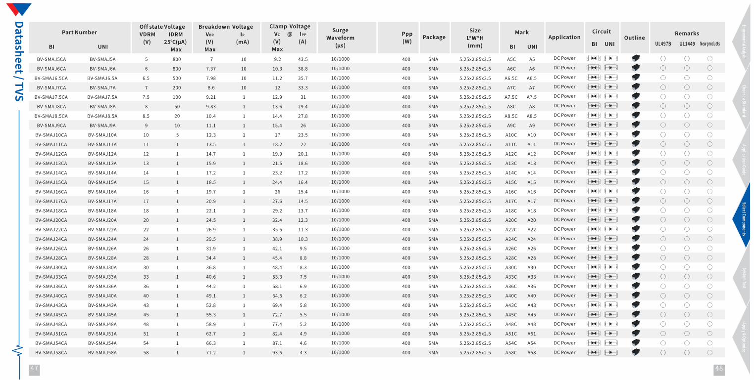
BV-SMAJ5CA
BV-SMAJ6CA
BV-SMAJ6.5CA
BV-SMAJ7CA
BV-SMAJ7.5CA
BV-SMAJ8CA
BV-SMAJ8.5CA
BV-SMAJ9CA
BV-SMAJ10CA
BV-SMAJ11CA
BV-SMAJ12CA
BV-SMAJ13CA
BV-SMAJ14CA
BV-SMAJ15CA
BV-SMAJ16CA
BV-SMAJ17CA
BV-SMAJ18CA
BV-SMAJ20CA
BV-SMAJ22CA
BV-SMAJ24CA
BV-SMAJ26CA
BV-SMAJ28CA
BV-SMAJ30CA
BV-SMAJ33CA
BV-SMAJ36CA
BV-SMAJ40CA
BV-SMAJ5A
BV-SMAJ6A
BV-SMAJ6.5A
BV-SMAJ7A
BV-SMAJ7.5A
BV-SMAJ8A
BV-SMAJ8.5A
BV-SMAJ9A
BV-SMAJ10A
BV-SMAJ11A
BV-SMAJ12A
BV-SMAJ13A
BV-SMAJ14A
BV-SMAJ15A
BV-SMAJ16A
BV-SMAJ17A
BV-SMAJ18A
BV-SMAJ20A
BV-SMAJ22A
BV-SMAJ24A
BV-SMAJ26A
BV-SMAJ28A
BV-SMAJ30A
BV-SMAJ33A
BV-SMAJ36A
BV-SMAJ40A
A5C
A6C
A6.5C
A7C
A7.5C
A8C
A8.5C
A9C
A10C
A11C
A12C
A13C
A14C
A15C
A16C
A17C
A18C
A20C
A22C
A24C
A26C
A28C
A30C
A33C
A36C
A40C
5
6
6.5
7
7.5
8
8.5
9
10
11
12
13
14
15
16
17
18
20
22
24
26
28
30
33
36
40
800
800
500
200
100
50
20
10
5
1
1
1
1
1
1
1
1
1
1
1
1
1
1
1
1
1
7
7.37
7.98
8.6
9.21
9.83
10.4
11.1
12.3
13.5
14.7
15.9
17.2
18.5
19.7
20.9
22.1
24.5
26.9
29.5
31.9
34.4
36.8
40.6
44.2
49.1
10
10
10
10
1
1
1
1
1
1
1
1
1
1
1
1
1
1
1
1
1
1
1
1
1
1
9.2
10.3
11.2
12
12.9
13.6
14.4
15.4
17
18.2
19.9
21.5
23.2
24.4
26
27.6
29.2
32.4
35.5
38.9
42.1
45.4
48.4
53.3
58.1
64.5
43.5
38.8
35.7
33.3
31
29.4
27.8
26
23.5
22
20.1
18.6
17.2
16.4
15.4
14.5
13.7
12.3
11.3
10.3
9.5
8.8
8.3
7.5
6.9
6.2
10/1000
10/1000
10/1000
10/1000
10/1000
10/1000
10/1000
10/1000
10/1000
10/1000
10/1000
10/1000
10/1000
10/1000
10/1000
10/1000
10/1000
10/1000
10/1000
10/1000
10/1000
10/1000
10/1000
10/1000
10/1000
10/1000
400
400
400
400
400
400
400
400
400
400
400
400
400
400
400
400
400
400
400
400
400
400
400
400
400
400
SMA
SMA
SMA
SMA
SMA
SMA
SMA
SMA
SMA
SMA
SMA
SMA
SMA
SMA
SMA
SMA
SMA
SMA
SMA
SMA
SMA
SMA
SMA
SMA
SMA
SMA
5.25x2.85x2.5
5.25x2.85x2.5
5.25x2.85x2.5
5.25x2.85x2.5
5.25x2.85x2.5
5.25x2.85x2.5
5.25x2.85x2.5
5.25x2.85x2.5
5.25x2.85x2.5
5.25x2.85x2.5
5.25x2.85x2.5
5.25x2.85x2.5
5.25x2.85x2.5
5.25x2.85x2.5
5.25x2.85x2.5
5.25x2.85x2.5
5.25x2.85x2.5
5.25x2.85x2.5
5.25x2.85x2.5
5.25x2.85x2.5
5.25x2.85x2.5
5.25x2.85x2.5
5.25x2.85x2.5
5.25x2.85x2.5
5.25x2.85x2.5
5.25x2.85x2.5
A5
A6
A6.5
A7
A7.5
A8
A8.5
A9
A10
A11
A12
A13
A14
A15
A16
A17
A18
A20
A22
A24
A26
A28
A30
A33
A36
A40
BV-SMAJ43CA
BV-SMAJ45CA
BV-SMAJ48CA
BV-SMAJ51CA
BV-SMAJ54CA
BV-SMAJ58CA
BV-SMAJ43A
BV-SMAJ45A
BV-SMAJ48A
BV-SMAJ51A
BV-SMAJ54A
BV-SMAJ58A
A43C
A45C
A48C
A51C
A54C
A58C
43
45
48
51
54
58
1
1
1
1
1
1
52.8
55.3
58.9
62.7
66.3
71.2
1
1
1
1
1
1
69.4
72.7
77.4
82.4
87.1
93.6
5.8
5.5
5.2
4.9
4.6
4.3
10/1000
10/1000
10/1000
10/1000
10/1000
10/1000
400
400
400
400
400
400
SMA
SMA
SMA
SMA
SMA
SMA
5.25x2.85x2.5
5.25x2.85x2.5
5.25x2.85x2.5
5.25x2.85x2.5
5.25x2.85x2.5
5.25x2.85x2.5
A43
A45
A48
A51
A54
A58
DC�Power
DC�Power
DC�Power
DC�Power
DC�Power
DC�Power
DC�Power
DC�Power
DC�Power
DC�Power
DC�Power
DC�Power
DC�Power
DC�Power
DC�Power
DC�Power
DC�Power
DC�Power
DC�Power
DC�Power
DC�Power
DC�Power
DC�Power
DC�Power
DC�Power
DC�Power
DC�Power
DC�Power
DC�Power
DC�Power
DC�Power
DC�Power
Datasheet�/�TVS
47 48
Part�Number SurgeWaveform
(μs)
Ppp(W)
SizeL*W*H(mm)
ApplicationCircuit
OutlinePackage Remarks
UL497B UL1449 New�productsBI��� UNI
Mark
BI��� UNI BI��� UNI
Environmental�AnalysisChoose�a�Standard
Application�GuideSelect�Components
System�TestApply�&�Optimize
Breakdown��Voltage������VBR�����������������������IR������(V)�������������������(mA)�����Max
Off�state�VoltageVDRM�����������IDRM���(V)�����������25℃(μA)��������������������������Max
��Clamp��Voltage������VC��������@������IPP�����(V)���������������(A)����Max

BV-SMAJ60CA
BV-SMAJ64CA
BV-SMAJ70CA
BV-SMAJ75CA
BV-SMAJ78CA
BV-SMAJ85CA
BV-SMAJ90CA
BV-SMAJ100CA
BV-SMAJ110CA
BV-SMBJ5CA
BV-SMBJ6CA
BV-SMBJ6.5CA
BV-SMAJ60A
BV-SMAJ64A
BV-SMAJ70A
BV-SMAJ75A
BV-SMAJ78A
BV-SMAJ85A
BV-SMAJ90A
BV-SMAJ100A
BV-SMAJ110A
BV-SMBJ5A
BV-SMBJ6A
BV-SMBJ6.5A
A60C
A64C
A70C
A75C
A78C
A85C
A90C
A100C
A110C
B5C
B6C
B6.5C
60
64
70
75
78
85
90
100
110
5
6
6.5
1
1
1
1
1
1
1
1
1
800
800
500
73.7
78.6
86
92.1
95.8
104
111
123
135
7
7.37
7.98
1
1
1
1
1
1
1
1
1
10
10
10
96.8
103
113
121
126
137
146
162
177
9.2
10.3
11.2
4.1
3.9
3.5
3.3
3.2
2.9
2.7
2.5
2.3
65.3
58.3
53.6
10/1000
10/1000
10/1000
10/1000
10/1000
10/1000
10/1000
10/1000
10/1000
10/1000
10/1000
10/1000
400
400
400
400
400
400
400
400
400
600
600
600
SMA
SMA
SMA
SMA
SMA
SMA
SMA
SMA
SMA
SMB
SMB
SMB
5.25x2.85x2.5
5.25x2.85x2.5
5.25x2.85x2.5
5.25x2.85x2.5
5.25x2.85x2.5
5.25x2.85x2.5
5.25x2.85x2.5
5.25x2.85x2.5
5.25x2.85x2.5
5.45x3.75x2.6
5.45x3.75x2.6
5.45x3.75x2.6
A60
A64
A70
A75
A78
A85
A90
A100
A110
B5
B6
B6.5
BV-SMBJ7CA
BV-SMBJ7.5CA
BV-SMBJ8CA
BV-SMBJ8.5CA
BV-SMBJ9CA
BV-SMBJ10CA
BV-SMBJ11CA
BV-SMBJ12CA
BV-SMBJ7A
BV-SMBJ7.5A
BV-SMBJ8A
BV-SMBJ8.5A
BV-SMBJ9A
BV-SMBJ10A
BV-SMBJ11A
BV-SMBJ12A
B7C
B7.5C
B8C
B8.5C
B9C
B10C
B11C
B12C
7
7.5
8
8.5
9
10
11
12
200
100
50
20
10
5
1
1
8.6
9.21
9.83
10.4
11.1
12.3
13.5
14.7
10
1
1
1
1
1
1
1
12
12.9
13.6
14.4
15.4
17
18.2
19.9
50
46.6
44.2
41.7
39
35.3
33
30.2
10/1000
10/1000
10/1000
10/1000
10/1000
10/1000
10/1000
10/1000
600
600
600
600
600
600
600
600
SMB
SMB
SMB
SMB
SMB
SMB
SMB
SMB
5.45x3.75x2.6
5.45x3.75x2.6
5.45x3.75x2.6
5.45x3.75x2.6
5.45x3.75x2.6
5.45x3.75x2.6
5.45x3.75x2.6
5.45x3.75x2.6
B7
B7.5
B8
B8.5
B9
B10
B11
B12
BV-SMBJ13CA
BV-SMBJ14CA
BV-SMBJ15CA
BV-SMBJ16CA
BV-SMBJ17CA
BV-SMBJ18CA
BV-SMBJ20CA
BV-SMBJ13A
BV-SMBJ14A
BV-SMBJ15A
BV-SMBJ16A
BV-SMBJ17A
BV-SMBJ18A
BV-SMBJ20A
B13C
B14C
B15C
B16C
B17C
B18C
B20C
13
14
15
16
17
18
20
1
1
1
1
1
1
1
15.9
17.2
18.5
19.7
20.9
22.1
24.5
1
1
1
1
1
1
1
21.5
23.2
24.4
26
27.6
29.2
32.4
28
25.9
24.6
23.1
21.8
20.6
18.6
10/1000
10/1000
10/1000
10/1000
10/1000
10/1000
10/1000
600
600
600
600
600
600
600
SMB
SMB
SMB
SMB
SMB
SMB
SMB
5.45x3.75x2.6
5.45x3.75x2.6
5.45x3.75x2.6
5.45x3.75x2.6
5.45x3.75x2.6
5.45x3.75x2.6
5.45x3.75x2.6
B13
B14
B15
B16
B17
B18
B20
BV-SMBJ22CA BV-SMBJ22A B22C22 1 26.9 1 35.5 16.9 10/1000 600 SMB 5.45x3.75x2.6 B22
BV-SMBJ24CA BV-SMBJ24A B24C24 1 29.5 1 38.9 15.5 10/1000 600 SMB 5.45x3.75x2.6 B24
BV-SMBJ26CA BV-SMBJ26A B26C26 1 31.9 1 42.1 14.3 10/1000 600 SMB 5.45x3.75x2.6 B26
BV-SMBJ28CA BV-SMBJ28A B28C28 1 34.4 1 45.4 13.3 10/1000 600 SMB 5.45x3.75x2.6 B28
BV-SMBJ30CA BV-SMBJ30A B30C30 1 36.8 1 48.4 12.4 10/1000 600 SMB 5.45x3.75x2.6 B30
DC�Power
DC�Power
DC�Power
DC�Power
DC�Power
DC�Power
DC�Power
DC�Power
DC�Power
DC�Power
DC�Power
DC�Power
DC�Power
DC�Power
DC�Power
DC�Power
DC�Power
DC�Power
DC�Power
DC�Power
DC�Power
DC�Power
DC�Power
DC�Power
DC�Power
DC�Power
DC�Power
DC�Power
DC�Power
DC�Power
DC�Power
DC�Power
49 50
Part�Number SurgeWaveform
(μs)
Ppp(W)
SizeL*W*H(mm)
Application OutlinePackage Remarks
UL497B UL1449 New�productsBI��� UNI
Mark
BI��� UNI
Circuit
BI��� UNI
Environmental�AnalysisChoose�a�Standard
Application�GuideSelect�Components
System�TestApply�&�Optimize
Datasheet�/�TVS
Breakdown��Voltage������VBR�����������������������IR������(V)�������������������(mA)�����Max
Off�state�VoltageVDRM�����������IDRM���(V)�����������25℃(μA)��������������������������Max
��Clamp��Voltage������VC��������@������IPP�����(V)���������������(A)����Max

BV-SMBJ33CA
BV-SMBJ36CA
BV-SMBJ40CA
BV-SMBJ43CA
BV-SMBJ45CA
BV-SMBJ48CA
BV-SMBJ51CA
BV-SMBJ54CA
BV-SMBJ58CA
BV-SMBJ60CA
BV-SMBJ64CA
BV-SMBJ70CA
BV-SMBJ75CA
BV-SMBJ78CA
BV-SMBJ33A
BV-SMBJ36A
BV-SMBJ40A
BV-SMBJ43A
BV-SMBJ45A
BV-SMBJ48A
BV-SMBJ51A
BV-SMBJ54A
BV-SMBJ58A
BV-SMBJ60A
BV-SMBJ64A
BV-SMBJ70A
BV-SMBJ75A
BV-SMBJ78A
B33C
B36C
B40C
B43C
B45C
B48C
B51C
B54C
B58C
B60C
B64C
B70C
B75C
B78C
33
36
40
43
45
48
51
54
58
60
64
70
75
78
1
1
1
1
1
1
1
1
1
1
1
1
1
1
40.6
44.2
49.1
52.8
55.3
58.9
62.7
66.3
71.2
73.7
78.6
86
92.1
95.8
1
1
1
1
1
1
1
1
1
1
1
1
1
1
53.3
58.1
64.5
69.4
72.7
77.4
82.4
87.1
93.6
96.8
103
113
121
126
11.3
10.4
9.3
8.7
8.3
7.8
7.3
6.9
6.5
6.2
5.9
5.3
5
4.8
10/1000
10/1000
10/1000
10/1000
10/1000
10/1000
10/1000
10/1000
10/1000
10/1000
10/1000
10/1000
10/1000
10/1000
600
600
600
600
600
600
600
600
600
600
600
600
600
600
SMB
SMB
SMB
SMB
SMB
SMB
SMB
SMB
SMB
SMB
SMB
SMB
SMB
SMB
5.45x3.75x2.6
5.45x3.75x2.6
5.45x3.75x2.6
5.45x3.75x2.6
5.45x3.75x2.6
5.45x3.75x2.6
5.45x3.75x2.6
5.45x3.75x2.6
5.45x3.75x2.6
5.45x3.75x2.6
5.45x3.75x2.6
5.45x3.75x2.6
5.45x3.75x2.6
5.45x3.75x2.6
B33
B36
B40
B43
B45
B48
B51
B54
B58
B60
B64
B70
B75
B78
BV-SMBJ85CA
BV-SMBJ90CA
BV-SMBJ100CA
BV-SMBJ110CA
BV-SMCJ5CA
BV-SMCJ6CA
BV-SMCJ6.5CA
BV-SMCJ7CA
BV-SMCJ7.5CA
BV-SMCJ8CA
BV-SMCJ8.5CA
BV-SMCJ9CA
BV-SMCJ10CA
BV-SMBJ85A
BV-SMBJ90A
BV-SMBJ100A
BV-SMBJ110A
BV-SMCJ5A
BV-SMCJ6A
BV-SMCJ6.5A
BV-SMCJ7A
BV-SMCJ7.5A
BV-SMCJ8A
BV-SMCJ8.5A
BV-SMCJ9A
BV-SMCJ10A
B85C
B90C
B100C
B110C
C5C
C6C
C6.5C
C7C
C7.5C
C8C
C8.5C
C9C
C10C
85
90
100
110
5
6
6.5
7
7.5
8
8.5
9
10
1
1
1
1
800
800
500
200
100
50
20
10
5
104
111
123
135
7
7.37
7.98
8.6
9.21
9.83
10.4
11.1
12.3
1
1
1
1
10
10
10
10
1
1
1
1
1
137
146
162
177
9.2
10.3
11.2
12
12.9
13.6
14.4
15.4
17
4.4
4.1
3.7
3.4
163.0
145.7
134.0
125.0
116.3
110.3
104.2
97.4
88.3
10/1000
10/1000
10/1000
10/1000
10/1000
10/1000
10/1000
10/1000
10/1000
10/1000
10/1000
10/1000
10/1000
600
600
600
600
1500
1500
1500
1500
1500
1500
1500
1500
1500
SMB
SMB
SMB
SMB
SMC
SMC
SMC
SMC
SMC
SMC
SMC
SMC
SMC
5.45x3.75x2.6
5.45x3.75x2.6
5.45x3.75x2.6
5.45x3.75x2.6
8.25x6.15x2.95
8.25x6.15x2.95
8.25x6.15x2.95
8.25x6.15x2.95
8.25x6.15x2.95
8.25x6.15x2.95
8.25x6.15x2.95
8.25x6.15x2.95
8.25x6.15x2.95
B85
B90
B100
B110
C5
C6
C6.5
C7
C7.5
C8
C8.5
C9
C10
BV-SMCJ11CA BV-SMCJ11A C11C11 1 13.5 1 18.2 82.5 10/1000 1500 SMC 8.25x6.15x2.95 C11
BV-SMCJ12CA BV-SMCJ12A C12C12 1 14.7 1 19.9 75.4 10/1000 1500 SMC 8.25x6.15x2.95 C12
BV-SMCJ13CA BV-SMCJ13A C13C13 1 15.9 1 21.5 69.8 10/1000 1500 SMC 8.25x6.15x2.95 C13
BV-SMCJ14CA BV-SMCJ14A C14C14 1 17.2 1 23.2 64.7 10/1000 1500 SMC 8.25x6.15x2.95 C14
BV-SMCJ15CA BV-SMCJ15A C15C15 1 18.5 1 24.4 61.5 10/1000 1500 SMC 8.25x6.15x2.95 C15
DC�Power
DC�Power
DC�Power
DC�Power
DC�Power
DC�Power
DC�Power
DC�Power
DC�Power
DC�Power
DC�Power
DC�Power
DC�Power
DC�Power
DC�Power
DC�Power
DC�Power
DC�Power
DC�Power
DC�Power
DC�Power
DC�Power
DC�Power
DC�Power
DC�Power
DC�Power
DC�Power
DC�Power
DC�Power
DC�Power
DC�Power
DC�Power
51 52
Part�Number SurgeWaveform
(μs)
Ppp(W)
SizeL*W*H(mm)
Application OutlinePackage Remarks
UL497B UL1449 New�productsBI��� UNI
Mark
BI��� UNI
Circuit
BI��� UNI
Environmental�AnalysisChoose�a�Standard
Application�GuideSelect�Components
System�TestApply�&�Optimize
Datasheet�/�TVS
Breakdown��Voltage������VBR�����������������������IR������(V)�������������������(mA)�����Max
Off�state�VoltageVDRM�����������IDRM���(V)�����������25℃(μA)��������������������������Max
��Clamp��Voltage������VC��������@������IPP�����(V)���������������(A)����Max
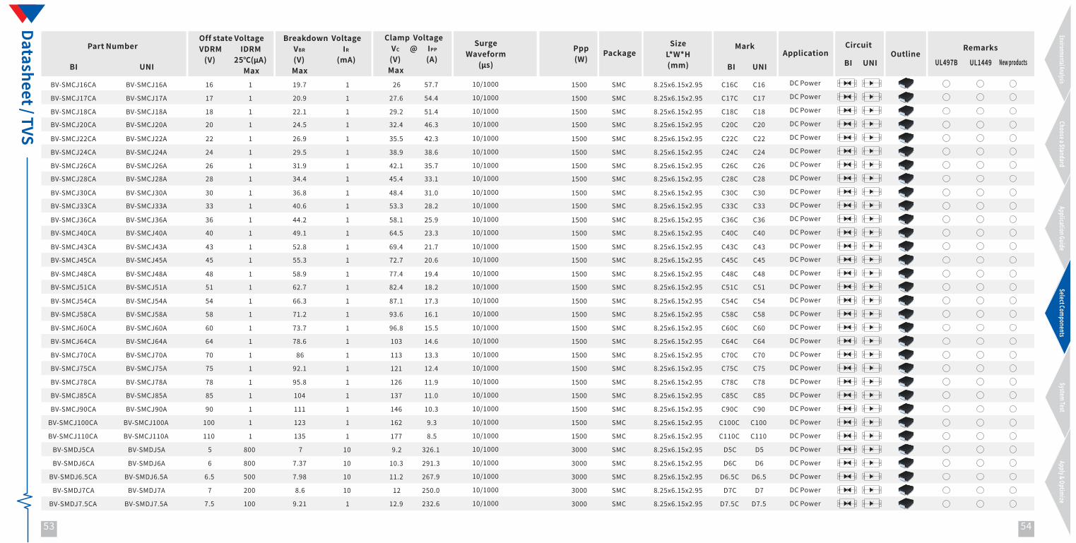
BV-SMCJ16CA
BV-SMCJ17CA
BV-SMCJ18CA
BV-SMCJ20CA
BV-SMCJ22CA
BV-SMCJ24CA
BV-SMCJ26CA
BV-SMCJ28CA
BV-SMCJ16A
BV-SMCJ17A
BV-SMCJ18A
BV-SMCJ20A
BV-SMCJ22A
BV-SMCJ24A
BV-SMCJ26A
BV-SMCJ28A
C16C
C17C
C18C
C20C
C22C
C24C
C26C
C28C
16
17
18
20
22
24
26
28
1
1
1
1
1
1
1
1
19.7
20.9
22.1
24.5
26.9
29.5
31.9
34.4
1
1
1
1
1
1
1
1
26
27.6
29.2
32.4
35.5
38.9
42.1
45.4
57.7
54.4
51.4
46.3
42.3
38.6
35.7
33.1
10/1000
10/1000
10/1000
10/1000
10/1000
10/1000
10/1000
10/1000
1500
1500
1500
1500
1500
1500
1500
1500
SMC
SMC
SMC
SMC
SMC
SMC
SMC
SMC
8.25x6.15x2.95
8.25x6.15x2.95
8.25x6.15x2.95
8.25x6.15x2.95
8.25x6.15x2.95
8.25x6.15x2.95
8.25x6.15x2.95
8.25x6.15x2.95
C16
C17
C18
C20
C22
C24
C26
C28
BV-SMCJ30CA
BV-SMCJ33CA
BV-SMCJ36CA
BV-SMCJ40CA
BV-SMCJ43CA
BV-SMCJ45CA
BV-SMCJ48CA
BV-SMCJ51CA
BV-SMCJ54CA
BV-SMCJ58CA
BV-SMCJ60CA
BV-SMCJ64CA
BV-SMCJ70CA
BV-SMCJ75CA
BV-SMCJ78CA
BV-SMCJ85CA
BV-SMCJ90CA
BV-SMCJ100CA
BV-SMCJ110CA
BV-SMCJ30A
BV-SMCJ33A
BV-SMCJ36A
BV-SMCJ40A
BV-SMCJ43A
BV-SMCJ45A
BV-SMCJ48A
BV-SMCJ51A
BV-SMCJ54A
BV-SMCJ58A
BV-SMCJ60A
BV-SMCJ64A
BV-SMCJ70A
BV-SMCJ75A
BV-SMCJ78A
BV-SMCJ85A
BV-SMCJ90A
BV-SMCJ100A
BV-SMCJ110A
C30C
C33C
C36C
C40C
C43C
C45C
C48C
C51C
C54C
C58C
C60C
C64C
C70C
C75C
C78C
C85C
C90C
C100C
C110C
30
33
36
40
43
45
48
51
54
58
60
64
70
75
78
85
90
100
110
1
1
1
1
1
1
1
1
1
1
1
1
1
1
1
1
1
1
1
36.8
40.6
44.2
49.1
52.8
55.3
58.9
62.7
66.3
71.2
73.7
78.6
86
92.1
95.8
104
111
123
135
1
1
1
1
1
1
1
1
1
1
1
1
1
1
1
1
1
1
1
48.4
53.3
58.1
64.5
69.4
72.7
77.4
82.4
87.1
93.6
96.8
103
113
121
126
137
146
162
177
31.0
28.2
25.9
23.3
21.7
20.6
19.4
18.2
17.3
16.1
15.5
14.6
13.3
12.4
11.9
11.0
10.3
9.3
8.5
10/1000
10/1000
10/1000
10/1000
10/1000
10/1000
10/1000
10/1000
10/1000
10/1000
10/1000
10/1000
10/1000
10/1000
10/1000
10/1000
10/1000
10/1000
10/1000
1500
1500
1500
1500
1500
1500
1500
1500
1500
1500
1500
1500
1500
1500
1500
1500
1500
1500
1500
SMC
SMC
SMC
SMC
SMC
SMC
SMC
SMC
SMC
SMC
SMC
SMC
SMC
SMC
SMC
SMC
SMC
SMC
SMC
8.25x6.15x2.95
8.25x6.15x2.95
8.25x6.15x2.95
8.25x6.15x2.95
8.25x6.15x2.95
8.25x6.15x2.95
8.25x6.15x2.95
8.25x6.15x2.95
8.25x6.15x2.95
8.25x6.15x2.95
8.25x6.15x2.95
8.25x6.15x2.95
8.25x6.15x2.95
8.25x6.15x2.95
8.25x6.15x2.95
8.25x6.15x2.95
8.25x6.15x2.95
8.25x6.15x2.95
8.25x6.15x2.95
C30
C33
C36
C40
C43
C45
C48
C51
C54
C58
C60
C64
C70
C75
C78
C85
C90
C100
C110
BV-SMDJ5CA BV-SMDJ5A D5C5 800 7 10 9.2 326.1 10/1000 3000 SMC 8.25x6.15x2.95 D5
BV-SMDJ6CA BV-SMDJ6A D6C6 800 7.37 10 10.3 291.3 10/1000 3000 SMC 8.25x6.15x2.95 D6
BV-SMDJ6.5CA BV-SMDJ6.5A D6.5C6.5 500 7.98 10 11.2 267.9 10/1000 3000 SMC 8.25x6.15x2.95 D6.5
BV-SMDJ7CA BV-SMDJ7A D7C7 200 8.6 10 12 250.0 10/1000 3000 SMC 8.25x6.15x2.95 D7
BV-SMDJ7.5CA BV-SMDJ7.5A D7.5C7.5 100 9.21 1 12.9 232.6 10/1000 3000 SMC 8.25x6.15x2.95 D7.5
DC�Power
DC�Power
DC�Power
DC�Power
DC�Power
DC�Power
DC�Power
DC�Power
DC�Power
DC�Power
DC�Power
DC�Power
DC�Power
DC�Power
DC�Power
DC�Power
DC�Power
DC�Power
DC�Power
DC�Power
DC�Power
DC�Power
DC�Power
DC�Power
DC�Power
DC�Power
DC�Power
DC�Power
DC�Power
DC�Power
DC�Power
DC�Power
53 54
Part�Number SurgeWaveform
(μs)
Ppp(W)
SizeL*W*H(mm)
Application OutlinePackage Remarks
UL497B UL1449 New�productsBI��� UNI
Mark
BI��� UNI
Circuit
BI��� UNI
Environmental�AnalysisChoose�a�Standard
Application�GuideSelect�Components
System�TestApply�&�Optimize
Datasheet�/�TVS
Breakdown��Voltage������VBR�����������������������IR������(V)�������������������(mA)�����Max
Off�state�VoltageVDRM�����������IDRM���(V)�����������25℃(μA)��������������������������Max
��Clamp��Voltage������VC��������@������IPP�����(V)���������������(A)����Max

BV-SMDJ8CA
BV-SMDJ8.5CA
BV-SMDJ8A
BV-SMDJ8.5A
D8C
D8.5C
8
8.5
50
20
9.83
10.4
1
1
13.6
14.4
220.6
208.3
10/1000
10/1000
3000
3000
SMC
SMC
8.25x6.15x2.95
8.25x6.15x2.95
D8
D8.5
BV-SMDJ9CA
BV-SMDJ10CA
BV-SMDJ11CA
BV-SMDJ12CA
BV-SMDJ13CA
BV-SMDJ14CA
BV-SMDJ15CA
BV-SMDJ9A
BV-SMDJ10A
BV-SMDJ11A
BV-SMDJ12A
BV-SMDJ13A
BV-SMDJ14A
BV-SMDJ15A
D9C
D10C
D11C
D12C
D13C
D14C
D15C
9
10
11
12
13
14
15
10
5
1
1
1
1
1
11.1
12.3
13.5
14.7
15.9
17.2
18.5
1
1
1
1
1
1
1
15.4
17
18.2
19.9
21.5
23.2
24.4
194.8
176.5
164.8
150.8
139.5
129.3
123.0
10/1000
10/1000
10/1000
10/1000
10/1000
10/1000
10/1000
3000
3000
3000
3000
3000
3000
3000
SMC
SMC
SMC
SMC
SMC
SMC
SMC
8.25x6.15x2.95
8.25x6.15x2.95
8.25x6.15x2.95
8.25x6.15x2.95
8.25x6.15x2.95
8.25x6.15x2.95
8.25x6.15x2.95
D9
D10
D11
D12
D13
D14
D15
BV-SMDJ16CA
BV-SMDJ17CA
BV-SMDJ18CA
BV-SMDJ20CA
BV-SMDJ22CA
BV-SMDJ24CA
BV-SMDJ26CA
BV-SMDJ28CA
BV-SMDJ30CA
BV-SMDJ33CA
BV-SMDJ36CA
BV-SMDJ40CA
BV-SMDJ43CA
BV-SMDJ45CA
BV-SMDJ48CA
BV-SMDJ51CA
BV-SMDJ54CA
BV-SMDJ58CA
BV-SMDJ16A
BV-SMDJ17A
BV-SMDJ18A
BV-SMDJ20A
BV-SMDJ22A
BV-SMDJ24A
BV-SMDJ26A
BV-SMDJ28A
BV-SMDJ30A
BV-SMDJ33A
BV-SMDJ36A
BV-SMDJ40A
BV-SMDJ43A
BV-SMDJ45A
BV-SMDJ48A
BV-SMDJ51A
BV-SMDJ54A
BV-SMDJ58A
D16C
D17C
D18C
D20C
D22C
D24C
D26C
D28C
D30C
D33C
D36C
D40C
D43C
D45C
D48C
D51C
D54C
D58C
16
17
18
20
22
24
26
28
30
33
36
40
43
45
48
51
54
58
1
1
1
1
1
1
1
1
1
1
1
1
1
1
1
1
1
1
19.7
20.9
22.1
24.5
26.9
29.5
31.9
34.4
36.8
40.6
44.2
49.1
52.8
55.3
58.9
62.7
66.3
71.2
1
1
1
1
1
1
1
1
1
1
1
1
1
1
1
1
1
1
26
27.6
29.2
32.4
35.5
38.9
42.1
45.4
48.4
53.3
58.1
64.5
69.4
72.7
77.4
82.4
87.1
93.6
115.4
108.7
102.7
92.6
84.5
77.1
71.3
66.1
62.0
56.3
51.6
46.5
43.2
41.3
38.8
36.4
34.4
32.1
10/1000
10/1000
10/1000
10/1000
10/1000
10/1000
10/1000
10/1000
10/1000
10/1000
10/1000
10/1000
10/1000
10/1000
10/1000
10/1000
10/1000
10/1000
3000
3000
3000
3000
3000
3000
3000
3000
3000
3000
3000
3000
3000
3000
3000
3000
3000
3000
SMC
SMC
SMC
SMC
SMC
SMC
SMC
SMC
SMC
SMC
SMC
SMC
SMC
SMC
SMC
SMC
SMC
SMC
8.25x6.15x2.95
8.25x6.15x2.95
8.25x6.15x2.95
8.25x6.15x2.95
8.25x6.15x2.95
8.25x6.15x2.95
8.25x6.15x2.95
8.25x6.15x2.95
8.25x6.15x2.95
8.25x6.15x2.95
8.25x6.15x2.95
8.25x6.15x2.95
8.25x6.15x2.95
8.25x6.15x2.95
8.25x6.15x2.95
8.25x6.15x2.95
8.25x6.15x2.95
8.25x6.15x2.95
D16
D17
D18
D20
D22
D24
D26
D28
D30
D33
D36
D40
D43
D45
D48
D51
D54
D58
BV-SMDJ60CA BV-SMDJ60A D60C60 1 73.7 1 96.8 31.0 10/1000 3000 SMC 8.25x6.15x2.95 D60
BV-SMDJ64CA BV-SMDJ64A D64C64 1 78.6 1 103 29.1 10/1000 3000 SMC 8.25x6.15x2.95 D64
BV-SMDJ70CA BV-SMDJ70A D70C70 1 86 1 113 26.5 10/1000 3000 SMC 8.25x6.15x2.95 D70
BV-SMDJ75CA BV-SMDJ75A D75C75 1 92.1 1 121 24.8 10/1000 3000 SMC 8.25x6.15x2.95 D75
BV-SMDJ78CA BV-SMDJ78A D78C78 1 95.8 1 126 23.8 10/1000 3000 SMC 8.25x6.15x2.95 D78
DC�Power
DC�Power
DC�Power
DC�Power
DC�Power
DC�Power
DC�Power
DC�Power
DC�Power
DC�Power
DC�Power
DC�Power
DC�Power
DC�Power
DC�Power
DC�Power
DC�Power
DC�Power
DC�Power
DC�Power
DC�Power
DC�Power
DC�Power
DC�Power
DC�Power
DC�Power
DC�Power
DC�Power
DC�Power
DC�Power
DC�Power
DC�Power
55 56
Part�Number SurgeWaveform
(μs)
Ppp(W)
SizeL*W*H(mm)
Application OutlinePackage Remarks
UL497B UL1449 New�productsBI��� UNI
Mark
BI��� UNI
Circuit
BI��� UNI
Environmental�AnalysisChoose�a�Standard
Application�GuideSelect�Components
System�TestApply�&�Optimize
Datasheet�/�TVS
Breakdown��Voltage������VBR�����������������������IR������(V)�������������������(mA)�����Max
Off�state�VoltageVDRM�����������IDRM���(V)�����������25℃(μA)��������������������������Max
��Clamp��Voltage������VC��������@������IPP�����(V)���������������(A)����Max

BV-SMDJ85CA
BV-SMDJ90CA
BV-SMDJ100CA
BV-SMDJ110CA
BV-5SMDJ11CA
BV-5�SMDJ12CA
�BV-5SMDJ13CA
BV-5SMDJ14CA
BV-5SMDJ15CA
BV-5SMDJ16CA
BV-5SMDJ17CA
BV-5SMDJ18CA
BV-5SMDJ20CA
BV-5SMDJ22CA
BV-5SMDJ24CA
BV-5SMDJ26CA
BV-5SMDJ28CA
BV-5SMDJ30CA
BV-5SMDJ33CA
BV-5SMDJ36CA
BV-5SMDJ40CA
BV-5SMDJ43CA
BV-SMDJ85A
BV-SMDJ90A
BV-SMDJ100A
BV-SMDJ110A
BV-5SMDJ11A
BV-5�SMDJ12A
BV-5SMDJ13A
BV-5SMDJ14A
BV-5SMDJ15A
BV-5SMDJ16A
BV-5SMDJ17A
BV-5SMDJ18A
BV-5SMDJ20A
BV-5SMDJ22A
BV-5SMDJ24A
BV-5SMDJ26A
BV-5SMDJ28A
BV-5SMDJ30A
BV-5SMDJ33A
BV-5SMDJ36A
BV-5SMDJ40A
BV-5SMDJ43A
D85C
D90C
D100C
D110C
5D11C
5D12C
5D13C
5D14C
5D15C
5D16C
5D17C
5D18C
5D20C
5D22C
5D24C
5D26C
5D28C
5D30C
5D33C
5D36C
5D40C
5D43C
85
90
100
110
11
12
13
14
15
16
17
18
20
22
24
26
28
30
33
36
40
43
1
1
1
1
800
800
500
200
100
50
20
10
5
5
2
2
2
2
2
2
2
2
104
111
123
135
13.5
14.7
15.9
17.2
18.5
19.7
20.9
22.1
24.5
26.9
29.5
31.9
34.4
36.8
40.6
44.2
49.1
52.8
1
1
1
1
1
1
1
1
1
1
1
1
1
1
1
1
1
1
1
1
1
1
137
146
162
177
18.2
19.9
21.5
23.2
24.4
26
27.6
29.2
32.4
35.5
38.9
42.1
45.4
48.4
53.3
58.1
64.5
69.4
21.9
20.5
18.5
16.9
275
252
233
216
205
193
181
172
155
141
129
119
110
103
93.9
86.1
77.6
72.1
10/1000
10/1000
10/1000
10/1000
10/1000
10/1000
10/1000
10/1000
10/1000
10/1000
10/1000
10/1000
10/1000
10/1000
10/1000
10/1000
10/1000
10/1000
10/1000
10/1000
10/1000
10/1000
3000
3000
3000
3000
5000
5000
5000
5000
5000
5000
5000
5000
5000
5000
5000
5000
5000
5000
5000
5000
5000
5000
SMC
SMC
SMC
SMC
SMC
SMC
SMC
SMC
SMC
SMC
SMC
SMC
SMC
SMC
SMC
SMC
SMC
SMC
SMC
SMC
SMC
SMC
8.25x6.15x2.95
8.25x6.15x2.95
8.25x6.15x2.95
8.25x6.15x2.95
8.25x6.15x2.95
8.25x6.15x2.95
8.25x6.15x2.95
8.25x6.15x2.95
8.25x6.15x2.95
8.25x6.15x2.95
8.25x6.15x2.95
8.25x6.15x2.95
8.25x6.15x2.95
8.25x6.15x2.95
8.25x6.15x2.95
8.25x6.15x2.95
8.25x6.15x2.95
8.25x6.15x2.95
8.25x6.15x2.95
8.25x6.15x2.95
8.25x6.15x2.95
8.25x6.15x2.95
D85
D90
D100
D110
5D11
5D12
5D13
5D14
5D15
5D16
5D17
5D18
5D20
5D22
5D24
5D26
5D28
5D30
5D33
5D36
5D40
5D43
BV-5SMDJ45CA
BV-5SMDJ48CA
BV-5SMDJ51CA
BV-5SMDJ54CA
BV-5SMDJ45A
BV-5SMDJ48A
BV-5SMDJ51A
BV-5SMDJ54A
5D45C
5D48C
5D51C
5D54C
45
48
51
54
2
2
2
2
55.3
58.9
62.7
66.3
1
1
1
1
72.7
77.4
82.4
87.1
68.8
64.7
60.7
57.5
10/1000
10/1000
10/1000
10/1000
5000
5000
5000
5000
SMC
SMC
SMC
SMC
8.25x6.15x2.95
8.25x6.15x2.95
8.25x6.15x2.95
8.25x6.15x2.95
5D45
5D48
5D51
5D54
BV-5SMDJ58CA BV-5SMDJ58A 5D58C58 2 71.2 1 93.6 53.5 10/1000 5000 SMC 8.25x6.15x2.95 5D58
BV-5SMDJ60CA BV-5SMDJ60A 5D60C60 2 73.7 1 96.8 51.7 10/1000 5000 SMC 8.25x6.15x2.95 5D60
BV-5SMDJ64CA BV-5SMDJ64A 5D64C64 2 78.6 1 103 48.6 10/1000 5000 SMC 8.25x6.15x2.95 5D64
BV-5SMDJ70CA BV-5SMDJ70A 5D70C70 2 86 1 113 44.3 10/1000 5000 SMC 8.25x6.15x2.95 5D70
BV-5SMDJ75CA BV-5SMDJ75A 5D75C75 2 92.1 1 121 41.4 10/1000 5000 SMC 8.25x6.15x2.95 5D75
BV-5SMDJ78CA BV-5SMDJ78A 5D78C78 2 95.8 1 126 39.7 10/1000 5000 SMC 8.25x6.15x2.95 5D78
DC�Power
DC�Power
DC�Power
DC�Power
DC�Power
DC�Power
DC�Power
DC�Power
DC�Power
DC�Power
DC�Power
DC�Power
DC�Power
DC�Power
DC�Power
DC�Power
DC�Power
DC�Power
DC�Power
DC�Power
DC�Power
DC�Power
DC�Power
DC�Power
DC�Power
DC�Power
DC�Power
DC�Power
DC�Power
DC�Power
DC�Power
DC�Power
57 58
Part�Number SurgeWaveform
(μs)
Ppp(W)
SizeL*W*H(mm)
Application OutlinePackage Remarks
UL497B UL1449 New�productsBI��� UNI
Mark
BI��� UNI
Circuit
BI��� UNI
Environmental�AnalysisChoose�a�Standard
Application�GuideSelect�Components
System�TestApply�&�Optimize
Datasheet�/�TVS
Breakdown��Voltage������VBR�����������������������IR������(V)�������������������(mA)�����Max
Off�state�VoltageVDRM�����������IDRM���(V)�����������25℃(μA)��������������������������Max
��Clamp��Voltage������VC��������@������IPP�����(V)���������������(A)����Max

25
BV-5SMDJ85CA
BV-5SMDJ90CA
BV-5SMDJ100CA
BV-5SMDJ110CA
BV-SMBT-15CA
BV-SMBT-20CA
BV-SMCT-30CA
BV-SMCT-58CA
BV-5SMDJ85A
BV-5SMDJ90A
BV-5SMDJ100A
BV-5SMDJ110A
5D85C
5D90C
5D100C
5D110C
B15CT
B20CT
C30CT
C58CT
85
90
100
110
15
20
30
58
2
2
2
2
1
1
1
1
104
111
123
135
18.5
24.5
36.8
71.2
1
1
1
1
1
1
1
1
137
146
162
177
24.4
32.4
48.4
93.6
36.5
34.3
30.9
28.3
40.8
30.8
62.0
32.1
10/1000
10/1000
10/1000
10/1000
10/1000
10/1000
10/1000
10/1000
5000
5000
5000
5000
1000(Pin1,3�to�2)
1000(Pin1,3�to�2)
3000(Pin1,3�to�2)
3000(Pin1,3�to�2)
SMC
SMC
SMC
SMC
SMB-T
SMB-T
SMC-T
SMC-T
8.25x6.15x2.95
8.25x6.15x2.95
8.25x6.15x2.95
8.25x6.15x2.95
5.4x3.3x2.0
5.4x3.3x2.0
8.0x5.9x2.0
8.0x5.9x2.0
5D85
5D90
5D100
5D110
DC�Power
DC�Power
DC�Power
DC�Power
DC�Power
DC�Power
POEPOE
59 60
BV-SMBJ58C2H
BV-SM8S24A
BV-SMBJ15CAH
B58C258 1 71.2 1 85 150 10/700 4(KV) SMB POE
SM8S24A24 5 29.5 5 38.9 170 10/1000 6600 DO-218AB 15.6x10.0x5.0
SB15CH15 1 18.5 1 24.4 40.8 10/1000 1000 SMB DC�Power
Automotive
Part�NumberBreakdown��Voltage������VBR�����������������������IR������(V)�������������������(mA)�����Max
��Clamp��Voltage������VC��������@������IPP�����(V)���������������(A)����Max
Off�state�VoltageVDRM�����������IDRM���(V)�����������25℃(μA)��������������������������Max
SurgeWaveform
(μs)
Ppp(W)
SizeL*W*H(mm)
Application OutlinePackage Remarks
UL497B UL1449 New�productsBI��� UNI
Mark
BI��� UNI
5.45x3.75x2.6
5.45x3.75x2.6
Circuit
BI��� UNI
Environmental�AnalysisChoose�a�Standard
Application�GuideSelect�Components
System�TestApply�&�Optimize
Datasheet�/�TVS
BV-SMEJ66CA
BV-SMEJ76CA
BV-SMEJ86CA
66
76
86
10
10
10
80
95
105
10
10
10
120���� 10KA@8/20
140
157
10KA@8/20
10KA@8/20
8/20
8/20
8/20
/ SME
SME
SME
18.3x14.0x7.5
18.3x14.0x7.5
18.3x14.0x7.5
BV10-66
BV10-76
BV10-86
DC�Power
DC�Power
DC�Power
BCCSP-58C-412K
BCCSP-58C-462K
58 1 66 10 93.6 10/7002KA@10/700 1500 CSP 4.1x4.1x0.6 58CSP DC�Power
58 1 66 10 93.6 10/7002KA@10/700 1500 CSP 4.6x4.6x0.6 58CSP DC�Power
BCCSP-58C-654K 58 1 66 10 93.6 10/7004KA@10/700 1500 CSP 4.6x4.6x0.6 58CSP DC�Power
/
/
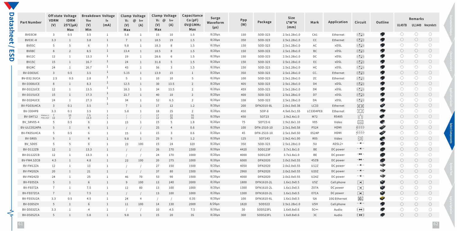
62
Datasheet�/�ESD
Part�Number
CapacitanceCo�(pF)
0V@1MHZ
Max
SurgeWaveform
(μs)
Ppp(W)
SizeL*W*H(mm)
Mark Application Circuit OutlinePackage
BV03CW
BV05C�
BV08C�
BV12C�
BV15C�
BV24C�
BV-D303UC
BV-D308UCE
BV-D312UCE
BV-D315UCE
BV-D324UCE
BV-FG03U4CA
BV-3304P8
BV_SRV05-4
BV-ULC0524PA
BV-FK05U4CA
BV-SR05
BV_SD05
BV-D112ZB
BV-FM12ZA
BV-FM20ZA
BV-FE05ZA
BV-D305ZH
BV-D50 ZC3 A
BV-D505ZCA
3
5
8
12
15
24
3
8
12
15
24
3
3.3
5
5
5
5
5
12
12
20
5
5
3.3
5
0.5
5
2
1
1
1
0.5
1
1
1
1
0.1
0.1
0.5
1
0.5
1
5
1
1
1
1
1
1
1
3.5
6
8.5
13.3
16.7
26.7
3.5
8.3
13.5
17.3
27.3
3.5
3.5
6
6
6
6
6
13.3
13
21
6
6
4
5.8
1
1
1
1
1
1
1
1
1
1
1
1
1
1
1
1
1
1
1
1
1
1
1
1
1
5.8
9.8
13.4
19
24
43
5.15
12.5
18.3
21.7
34
7
5.8
15
/
15
9.8
23
23
/
9
11
10
9.8
1
1
1
1
1
1
1
1
1
1
1
1
1
1
/
1
1
100
100
/
100
4.5
1
15
18.3
18.5
28.6
31.8
56
13.9
30
34
40
52
17
18
15
25
15
25
15
26
27
37
13
15
10
8
8
6
5
3
15
13.5
13.5
10
6.5
12
25
5
4
3
5
24
170
150
80
140
20
1.5
1.5
1.5
1.5
1.5
1.5
1
2
2
2
2
1.2
2
1.8
0.6
0.6
1.2
320
1500
1500
1500
2000
7.5
35
8/20μs
8/20μs
8/20μs
8/20μs
8/20μs
8/20μs
8/20μs
8/20μs
8/20μs
8/20μs
8/20μs
8/20μs
8/20μs
8/20μs
8/20μs
8/20μs
8/20μs
8/20μs
8/20μs
8/20μs
8/20μs
8/20μs
8/20μs
150
150
150
150
150
150
350
405
459
400
338
200
450
75
100
45
125
350
4420
4050
2960
1800
50
300
SOD-323
SOD-323
SOD-323
SOD-323
SOD-323
SOD-323
SOD-323
SOD-323
SOD-323
SOD-323
SOD-323
DFN2010-8L
SOP-8
SOT23-6
DFN-2510-10
DFN-2510-10
SOT143
SOD-323
SOD123F
DFN2020
DFN2020
DFN1610-2L
SOD523FL
SOD523FL
2.5 1.28 1.0x x
2.5 1.28 1.0x x
2.5 1.28 1.0x x
2.5 1.28 1.0x x
2.5 1.28 1.0x x
2.5 1.28 1.0x x
2.5 1.28 1.0x x
2.5x1.28x1.0
2.5x1.28x1.0
2.5x1.28x1.0
2.5x1.28x1.0
2.0x1.0x0.38
4.9x6.0x1.55
2.9x2.8x1.10
2.5x1.0x0.58
2.5x1.0x0.50
2.9x2.4x1.00
2.5x1.28x1.0
3.7x1.8x1.0
2.0 2.0 0.55x x
2.0x2.0x0.55
1.6 1.0 0.5x x
1.6 0.8 0.6x x
1.6 0.8 0.6x x
CA1
AC
BC
DC
EC
HC
CC.
D4
DK
D7
DA
LC33
LC3304PE8
V05
P524
0524P
R05
5U
BE
U12Z
U20Z
U5Z
5C∞
Ethernet
xDSL
xDSL
xDSL
xDSL
xDSL
Ethernet
xDSL
xDSL
xDSL
xDSL
Ethernet
Ethernet
Video
HDMI
HDMI
Video
ADSL2+
DC�power
DC�power
DC�power
Cell�phone
Audio
Audio
100 14 130 2000
8/20μs
1820 SOD323 2.5 1.28 1.0x x U5H
CC
Cell�phone
Remarks
UL497B UL1449 New�products
BV-SM712 1 8/20μs 450 2.9x2.4x1.0 M72712
102
7.513.3 1
1712
2226 SOT23 RS485PIN3to1,2
PIN1,2to3
BV-FE03U2A 3.3 0.5 4.5 1 24 4 0.35
8/20μs
100 DFN1610-6L 1.6 1.0 0.5x x GA 10G�Ethernet/ /456
1 2 3
Environmental�AnalysisChoose�a�Standard
Application�GuideSelect�Components
System�TestApply�&�Optimize
BV03C-H 3.3 1 3.8 1 7 1 18.5 19 1.5 8/20μs 350 SOD-323 2.5x1.28x1.0 CC Ethernet
BV-D32.5UCA 2.5 0.5 2.8 1 5 1 10 8/20μs SOD-323 2.5x1.28x1.0 ZC Ethernet10 5 100
BV-D112ZCB 12 1 13.3 1 24 170 1000 8/20μs 4000 SOD123F 3.7x1.8x1.0 BE DC�power
BV-FM4.5ZCB 4.5 1 4.8 1 20 275 1000 8/20μs 6000 45ZB DC�power
/ /
/ /
/ /
8/20μs
BV-FM24ZD 24 1 25 1 53 90 1500 8/20μs 4000 DFN2020 2.0x2.0x0.55 U24Z DC�power46 70
BV-FE07ZA 7 1 7.5 1 12 80 13 100 1000
8/20μs
1300 DFN1610-2L 1.6x1.0x0.5 Z07A DC�power
BV-FE07ZCA 1 1 13
8/20μs
DFN1610-2L 1.6x1.0x0.5 07CA7 7.5 / / 100 1000 1300 DC�power
/ 5555
DFN2020 2.0 2.0 0.55x x
///
/ /
61
�����Off�state��Voltage������VDRM�����������IDRM���������(V)�����������25℃(μA)�������������������������������Max
Breakdown��Voltage������VBR���������������������IR������(V)�����������������(mA)�����Min
Clamp��Voltage������VC��������@����IPP�����(V)�������������(A)����Max
Clamp��Voltage������VC������@�����IPP�����(V)������������(A)����Max

63 64
BV-D305UA
BV-E505U2A
BV-F603UCA
BV-D303ZCA
BV-D305ZCA
BV-D308ZCA
BV-D312ZCA
BV-D315ZCA
BV-D318ZCA
BV-D324ZCA
BV-D336ZCA
BV-D303ZB
BV-D305ZB
BV-D312ZB
5
5
3.3
3.3
5
8
12
15
18
24
36
3.3
5
12
1
1
0.05
40
1
1
1
1
1
1
1
40
10
1
6
6
6
4
6
8.5
13.3
16.7
19.5
26.7
40
4
6
13.3
1
1
1
1
1
1
1
1
1
1
1
1
1
1
10
12
/
7.5
9.8
13.4
20
25
30
45
65
8
9.8
22
1
1
/
1
1
1
1
1
1
1
1
1
1
1
20
25
12
16
17
20
30
36
40
50
75
11
18
32
44
3.5
25
24
18
11
9
8
5
3
18
17
11
0.8
0.8
0.35
200
200
100
50
45
42
40
25
450
400
130
8/20μs
8/20μs
8/20μs
8/20μs
8/20μs
8/20μs
8/20μs
8/20μs
8/20μs
8/20μs
8/20μs
8/20μs
8/20μs
8/20μs
80
100
42
400
408
360
330
324
320
250
225
198
306
352
SOD323
DFN0603-2L
SOD-323
SOD-323
SOD-323
SOD-323
SOD-323
SOD-323
SOD-323
SOD-323
SOD-323
SOD-323
SOD-323
2.5 1.28 1.0x x
1.6x1.6x0.75
0.6x0.3x0.3
2.5 1.28 1.0x x
2.5x1.28x1.0
2.5x1.28x1.0
2.5x1.28x1.0
2.5x1.28x1.0
2.5x1.28x1.0
2.5x1.28x1.0
2.5x1.28x1.0
2.5x1.28x1.0
2.5x1.28x1.0
2.5x1.28x1.0
LLP5
JD
2A
2B
2C
2D
2J
2K
2H
2N
03W
05W
12W
DC�powereSATA
USB3.0
DC�power
DC�power
DC�power
DC�power
DC�power
DC�power
DC�power
DC�power
DC�power
DC�power
DC�power
SOT523
Part�Number
CapacitanceCo�(pF)
0V@1MHZ
Max
SurgeWaveform
(μs)
Ppp(W)
SizeL*W*H(mm)
Mark Application Circuit OutlinePackageRemarks
UL497B UL1449 New�products
BV-FA05UA� 5 1 5.4 1 10 1 20 4 0.8 8/20μs 80 DFN1006-2L 1.0 0.6 0.5x x L DC�power
Environmental�AnalysisChoose�a�Standard
Application�GuideSelect�Components
System�TestApply�&�Optimize
Datasheet�/�ESD
BV-FA03ZCB 3.3 1 3.5 1 6 1 10 7 15 8/20μs 70 DFN1006-2L 1.0 0.6 0.5x x T Ethernet
BV-D512ZA�
BV-FA05UC
BV-FA05ZC
BV-FA08ZCA
BV-FA12ZCA
BV-FA15ZCA
12
5
5
8
12
15
0.1
1
1
1
1
1
14.1
6
6
8.5
13.3
16.7
1
1
1
1
1
1
23
12
11
11
17
21
3
1
1
1
1
1
29
14
15
22
30
37
6
2
4.5
10
6
5
100
0.5
15
50
30
30
8/20μs
8/20μs
8/20μs
8/20μs
8/20μs
8/20μs
174
25
75
220
180
185
SOD523FL
DFN1006-2L
DFN1006-2L
DFN1006-2L
DFN1006-2L
DFN1006-2L
1.6x0.8x0.6
1.0 0.6 0.5x x
1.0 0.6 0.5x x
1.0 0.6 0.5x x
1.0 0.6 0.5x x
1.0 0.6 0.5x x
ZM
S
PB
D8
DD
DE
DC
HDMI
Cell�phone
DC
DC
DC
BV-FA2.5UCB 2.5 0.5 2.8 1 5 10 5 8/20μs 100 DFN1006-2 1.0x0.6x0.5 2V5Z Ethernet1 10
BV-FA05UCA 5 0.1 6 1 16 2 24 4 0.4 8/20μs 96 DFN1006-2 1.0x0.6x0.5 5BU HDMI
BV-FA05UCB
BV-FA05UCD
5
5
0.05
0.05
6
6
1
1TYP:8.3
9
1
1
TYP:10
11
4
7
0.5 8/20μs
8/20μs40
77
1.0x0.6x0.5
1.0x0.6x0.5
5U
5T
HDMI
HDMI1
DFN1006-2
DFN1006-2
BV-FA03ZCD 1 1 7.6 1 15 6 15 8/20μs 75 DFN1006-2L 1.0x0.6x0.5 3X
BV-FA05ZCD 0.5 1 10 1 12 5 18 8/20μs 75 DFN1006-2L 1.0x0.6x0.5 PD
BV-FA814ZCB 13 8/20μs 100 DFN1006-2L 1.0x0.6x0.5 8E
3.3
5814
11
4
5.68.514.5
//
//
TYP:24TYP:25.5
33
PDA
PDADC�power
BV-FW05U6CA 5 1 1 16 1 0.35 8/20μs 20 DFN4120-10L 4.1x2.0x0.5 BCN*** HDMI6 / /
BV-E505U2B 5 0.1 6 1 12 1 15 4 0.8 8/20μs 60 1.6x1.6x0.75 52L eSATASOT523
BV-D34.5ZCA 4.5 4.8 1 16 8/20μs 2200 2.5x1.28x1.0 48D1 13 100 160 1500 SOD-323 DC�power
11
BV-D505ZCB 5 2 5.2 1 9.8 1 16 3 7 8/20μs 50 SOD523FL 1.6x0.8x0.6 LB Audio
BV-D505ZC 5 1 5.6 1 11.6 5 19 8 15 150 SOD523FL 1.6 0.8 0.6x x 5C∞ Audio8/20μs
�����Off�state��Voltage������VDRM�����������IDRM���������(V)�����������25℃(μA)�������������������������������Max
Breakdown��Voltage������VBR���������������������IR������(V)�����������������(mA)�����Min
Clamp��Voltage������VC��������@����IPP�����(V)�������������(A)����Max
Clamp��Voltage������VC������@�����IPP�����(V)������������(A)����Max

65 66
Part�Number
Breakdown��Voltage������VBR���������������������IR������(V)�����������������(mA)�����Min
Clamp��Voltage������VC��������@����IPP�����(V)�������������(A)����Max
CapacitanceCo�(pF)
0V@1MHZ
Max
Clamp��Voltage������VC������@�����IPP�����(V)������������(A)����Max
SurgeWaveform
(μs)
Ppp(W)
SizeL*W*H(mm)
Mark Application Circuit OutlinePackageRemarks
UL497B UL1449 New�products
Environmental�AnalysisChoose�a�Standard
Application�GuideSelect�Components
System�TestApply�&�Optimize
Datasheet�/�ESD
BV-T318Z2CA
BV-T324Z2CA
BV-T333Z2CA
BV-T336Z2CA
BV-T303Z2B
BV-T305Z2B
BV-T312Z2B
BV-T315Z2B
BV-T324Z2B
BV-T336Z2B
BV-P806Z2
BV-P803Z2A
18
24
33
36
3.3
5
12
15
24
36
6
3.3
1
1
1
1
40
10
1
1
1
1
25
1
20
26.7
34.6
40
4
6
13.3
16.7
26.7
40
6.8
3.5
1
1
1
1
1
1
1
1
1
1
1
0.002
30
45
58
65
7.5
9.8
22
24
43
60
14
/
1
1
1
1
1
1
1
1
1
1
25
/
40
50
60
75
12
18
32
38
52
75
20
20
8
5
4
3
20
17
11
10
5.5
3
100
100
45
40
30
25
450
400
130
120
80
60
20
25
8/20μs
8/20μs
8/20μs
8/20μs
8/20μs
8/20μs
8/20μs
8/20μs
8/20μs
8/20μs
8/20μs
8/20μs
320
250
240
225
240
306
352
380
286
225
2000
2000
SOP8
SOP8
2.9x2.4x1.0
2.9x2.4x1.0
2.9x2.4x1.0
2.9x2.4x1.0
2.9x2.4x1.0
2.9x2.4x1.0
2.9x2.4x1.0
2.9x2.4x1.0
2.9x2.4x1.0
2.9x2.4x1.0
4.9 6.0 1.55x x
4.9 6.0 1.55x x
C18
C24
C33
C36
M03
M05
M12
M15
M24
M36
0306
LC03-3.31 2 3 4
5678
DC�power
DC�power
DC�power
DC�power
DC�power
DC�power
DC�power
DC�power
DC�power
DC�power
Ethernet
Ethernet
SOT23
SOT23
SOT23
SOT23
SOT23
SOT23
SOT23
SOT23
SOT23
SOT23
BV-T315Z2CA 15 1 16.7 1 25 1 36 9 45 8/20μs 324 2.9x2.4x1.0 C15 DC�powerSOT23
BV-T308Z2CA
BV-T312Z2CA
8
12
1
1
8.5
13.3
1
1
13.4
20
1
1
20
30
18
11
100
50
8/20μs
8/20μs
360
330
2.9x2.4x1.0
2.9x2.4x1.0
C08
C12
DC�power
DC�powerSOT23
SOT23
BV-D324ZB
BV-D336ZB
BV-T305Z2CA
24
36
5
1
1
5
26.7
40
6
1
1
1
43
60
9.8
1
1
1
52
75
17
5.5
3
24
80
60
200
8/20μs
8/20μs
8/20μs
286
225
400
SOD-323
SOD-323
2.5x1.28x1.0
2.5x1.28x1.0
2.9x2.4x1.0
24W
36W
C05
DC�powerDC�power
DC�powerSOT23
BV-T305U2A 5 0.1 6 1 10 1 15 4 0.4 8/20μs 60 2.9x2.4x1.0 52L eSATASOT23
BV-P858Z4A 58 0.5 62 1 / / 100 24 400 8/20μs 2400 SOP8 4.9x6.0x1.55 Z58A DC�power
BV-D315ZB 15 1 16.7 1 24 1 38 10 120 8/20μs 380 SOD-323 2.5x1.28x1.0 15W DC�power
�����Off�state��Voltage������VDRM�����������IDRM���������(V)�����������25℃(μA)�������������������������������Max

67 68
Part�NumberBreakdown��Voltage
������VBR���������������IR
������min(V)����������� (mA)
SurgeWaveform
(μs)
Ppp(W)
SizeL*W*H(mm)
Application OutlinePackage
BI��� UNI
Mark
BI��� UNI
Circuit
BI��� UNI
BV-D105ZCF
BV-D106ZCF
BV-D16.5ZCF
BV-D107ZCF
BV-D17.5ZCF
BV-D108ZCF
BV-D18.5ZCF
BV-D109ZCF
BV-D110ZCF
BV-D111ZCF
BV-D112ZCF
BV-D113ZCF
BV-D114ZCF
BV-D115ZCF
BV-D116ZCF
BV-D117ZCF
BV-D118ZCF
BV-D120ZCF
BV-D122ZCF
BV-D124ZCF
BV-D126ZCF
BV-D128ZCF
BV-D130ZCF
BV-D133ZCF
BV-D136ZCF
BV-D140ZCF
BV-D143ZCF
BV-D145ZCF
BV-D148ZCF
BV-D151ZCF
BV-D154ZCF
BV-D158ZCF
BV-D160ZCF
BV-D164ZCF
BV-D105ZF
BV-D106ZF
BV-D16.5ZF
BV-D107ZF
BV-D17.5ZF
BV-D108ZF
BV-D18.5ZF
BV-D109ZF
BV-D110ZF
BV-D111ZF
BV-D112ZF
BV-D113ZF
BV-D114ZF
BV-D115ZF
BV-D116ZF
BV-D117ZF
BV-D118ZF
BV-D120ZF
BV-D122ZF
BV-D124ZF
BV-D126ZF
BV-D128ZF
BV-D130ZF
BV-D133ZF
BV-D136ZF
BV-D140ZF
BV-D143ZF
BV-D145ZF
BV-D148ZF
BV-D151ZF
BV-D154ZF
BV-D158ZF
BV-D160ZF
BV-D164ZF
5
6
6.5
7
7.5
8
8.5
9
10
11
12
13
14
15
16
17
18
20
22
24
26
28
30
33
36
40
43
45
48
51
54
58
60
64
800
800
500
200
100
50
20
10
5
3
1
1
1
1
1
1
1
1
1
1
1
1
1
1
1
1
1
1
1
1
1
1
1
1
6.4
6.67
7.22
7.78
8.33
8.89
9.44
10
11.1
12.2
13.3
14.4
15.6
16.7
17.8
18.9
20
22.2
24.4
26.7
28.9
31.1
33.3
36.7
40
44.4
47.8
50
53.3
56.7
60
64.4
66.7
71.1
7
7.37
7.98
8.6
9.21
9.83
10.4
11.1
12.3
13.5
14.7
15.9
17.2
18.5
19.7
20.9
22.1
24.5
26.9
29.5
31.9
34.4
36.8
40.6
44.2
49.1
52.8
55.3
58.9
62.7
66.3
71.2
73.7
78.6
10
10
10
10
1
1
1
1
1
1
1
1
1
1
1
1
1
1
1
1
1
1
1
1
1
1
1
1
1
1
1
1
1
1
9.2
10.3
11.2
12
12.9
13.6
14.4
15.4
17
18.2
19.9
21.5
23.2
24.4
26
27.6
29.2
32.4
35.5
38.9
42.1
45.4
48.4
53.3
58.1
64.5
69.4
72.7
77.4
82.4
87.1
93.6
96.8
103
21.8
19.4
17.9
16.7
15.5
14.7
13.9
13
11.8
11
10.1
9.3
8.6
8.2
7.7
7.3
6.9
6.2
5.7
5.2
4.8
4.4
4.2
3.8
3.5
3.1
2.9
2.8
2.6
2.5
2.3
2.3
2.1
2
10/1000uS
10/1000uS
10/1000uS
10/1000uS
10/1000uS
10/1000uS
10/1000uS
10/1000uS
10/1000uS
10/1000uS
10/1000uS
10/1000uS
10/1000uS
10/1000uS
10/1000uS
10/1000uS
10/1000uS
10/1000uS
10/1000uS
10/1000uS
10/1000uS
10/1000uS
10/1000uS
10/1000uS
10/1000uS
10/1000uS
10/1000uS
10/1000uS
10/1000uS
10/1000uS
10/1000uS
10/1000uS
10/1000uS
10/1000uS
200
200
200
200
200
200
200
200
200
200
200
200
200
200
200
200
200
200
200
200
200
200
200
200
200
200
200
200
200
200
200
200
200
200
SOD123F
SOD123F
SOD123F
SOD123F
SOD123F
SOD123F
SOD123F
SOD123F
SOD123F
SOD123F
SOD123F
SOD123F
SOD123F
SOD123F
SOD123F
SOD123F
SOD123F
SOD123F
SOD123F
SOD123F
SOD123F
SOD123F
SOD123F
SOD123F
SOD123F
SOD123F
SOD123F
SOD123F
SOD123F
SOD123F
SOD123F
SOD123F
SOD123F
SOD123F
3.7x1.8x1.0
3.7x1.8x1.0
3.7x1.8x1.0
3.7x1.8x1.0
3.7x1.8x1.0
3.7x1.8x1.0
3.7x1.8x1.0
3.7x1.8x1.0
3.7x1.8x1.0
3.7x1.8x1.0
3.7x1.8x1.0
3.7x1.8x1.0
3.7x1.8x1.0
3.7x1.8x1.0
3.7x1.8x1.0
3.7x1.8x1.0
3.7x1.8x1.0
3.7x1.8x1.0
3.7x1.8x1.0
3.7x1.8x1.0
3.7x1.8x1.0
3.7x1.8x1.0
3.7x1.8x1.0
3.7x1.8x1.0
3.7x1.8x1.0
3.7x1.8x1.0
3.7x1.8x1.0
3.7x1.8x1.0
3.7x1.8x1.0
3.7x1.8x1.0
3.7x1.8x1.0
3.7x1.8x1.0
3.7x1.8x1.0
3.7x1.8x1.0
AE
AG
AK
AM
AP
AR
AT
AV
AX
AZ
BE
BG
BK
BM
BP
BR
BT
BV
BX
BZ
CE
CG
CK
CM
CP
CR
CT
CV
CX
CZ
DE
DG
DK
DM
lAE
lAG
lAK
lAM
lAP
lAR
lAT
lAV
lAX
lAZ
lBE
lBG
lBK
lBM
lBP
lBR
lBT
lBV
lBX
lBZ
lCE
lCG
lCK
lCM
lCP
lCR
lCT
lCV
lCX
lCZ
lDE
lDG
lDK
lDM
DC�power
DC�power
DC�power
DC�power
DC�power
DC�power
DC�power
DC�power
DC�power
DC�power
DC�power
DC�power
DC�power
DC�power
DC�power
DC�power
DC�power
DC�power
DC�power
DC�power
DC�power
DC�power
DC�power
DC�power
DC�power
DC�power
DC�power
DC�power
DC�power
DC�power
DC�power
DC�power
DC�power
DC�power
�����Max.(V)
Remarks
UL497B UL1449 New�products
Environmental�AnalysisChoose�a�Standard
Application�GuideSelect�Components
System�TestApply�&�Optimize
Datasheet�/�ESD
�����Off�state��Voltage������VDRM�����������IDRM���������(V)�����������25℃(μA)�������������������������������Max
Clamp��Voltage������VC�����@����IPP�����(V)����������(A)����Max
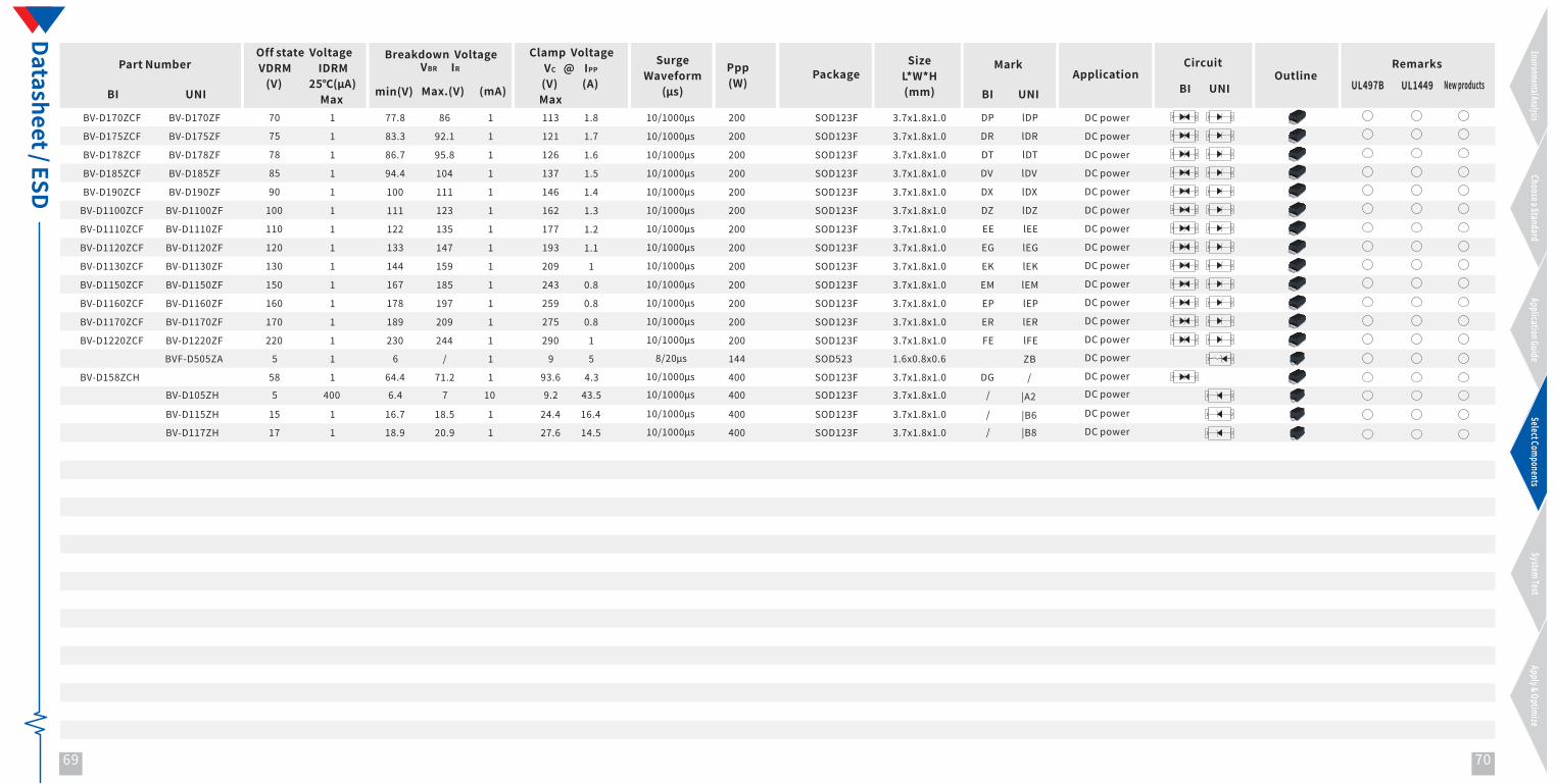
Part�NumberBreakdown��Voltage
������VBR���������������IR
������min(V)����������� (mA)
Clamp��Voltage������VC�����@����IPP�����(V)����������(A)����Max
�����Off�state��Voltage������VDRM�����������IDRM���������(V)�����������25℃(μA)�������������������������������Max
SurgeWaveform
(μs)
Ppp(W)
SizeL*W*H(mm)
Application OutlinePackage
BI��� UNI
Mark
BI��� UNI
Circuit
BI��� UNI�����Max.(V)
Remarks
UL497B UL1449 New�products
69 70
BV-D170ZCF
BV-D175ZCF
BV-D178ZCF
BV-D185ZCF
BV-D190ZCF
BV-D1100ZCF
BV-D1110ZCF
BV-D1120ZCF
BV-D1130ZCF
BV-D1150ZCF
BV-D1160ZCF
BV-D1170ZCF
BV-D1220ZCF
BV-D170ZF
BV-D175ZF
BV-D178ZF
BV-D185ZF
BV-D190ZF
BV-D1100ZF
BV-D1110ZF
BV-D1120ZF
BV-D1130ZF
BV-D1150ZF
BV-D1160ZF
BV-D1170ZF
BV-D1220ZF
70
75
78
85
90
100
110
120
130
150
160
170
220
1
1
1
1
1
1
1
1
1
1
1
1
1
77.8
83.3
86.7
94.4
100
111
122
133
144
167
178
189
230
86
92.1
95.8
104
111
123
135
147
159
185
197
209
244
1
1
1
1
1
1
1
1
1
1
1
1
1
113
121
126
137
146
162
177
193
209
243
259
275
290
1.8
1.7
1.6
1.5
1.4
1.3
1.2
1.1
1
0.8
0.8
0.8
1
10/1000μs
10/1000μs
10/1000μs
10/1000μs
10/1000μs
10/1000μs
10/1000μs
10/1000μs
10/1000μs
10/1000μs
10/1000μs
10/1000μs
10/1000μs
200
200
200
200
200
200
200
200
200
200
200
200
200
SOD123F
SOD123F
SOD123F
SOD123F
SOD123F
SOD123F
SOD123F
SOD123F
SOD123F
SOD123F
SOD123F
SOD123F
SOD123F
3.7x1.8x1.0
3.7x1.8x1.0
3.7x1.8x1.0
3.7x1.8x1.0
3.7x1.8x1.0
3.7x1.8x1.0
3.7x1.8x1.0
3.7x1.8x1.0
3.7x1.8x1.0
3.7x1.8x1.0
3.7x1.8x1.0
3.7x1.8x1.0
3.7x1.8x1.0
DP
DR
DT
DV
DX
DZ
EE
EG
EK
EM
EP
ER
FE
lDP
lDR
lDT
lDV
lDX
lDZ
lEE
lEG
lEK
lEM
lEP
lER
lFE
DC�power
DC�power
DC�power
DC�power
DC�power
DC�power
DC�power
DC�power
DC�power
DC�power
DC�power
DC�power
DC�power
BVF-D505ZA 5 1 6 / 1 9 5 8/20μs 144 SOD523 1.6x0.8x0.6 ZB DC�power
Environmental�AnalysisChoose�a�Standard
Application�GuideSelect�Components
System�TestApply�&�Optimize
Datasheet�/�ESD
BV-D158ZCH 58 1 64.4 71.2 1 93.6
9.2
24.4
27.6
4.3
43.5
16.4
14.5
10/1000μs 400 SOD123F 3.7x1.8x1.0 DG DC�power
BV-D105ZH
BV-D115ZH
BV-D117ZH
5
15
17
400
1
1
6.4
16.7
18.9
7
18.5
20.9
10
1
1
10/1000μs
10/1000μs
10/1000μs
400
400
400
SOD123F
SOD123F
SOD123F
3.7x1.8x1.0
3.7x1.8x1.0
3.7x1.8x1.0
|A2
|B6|B8
DC�power
DC�power
DC�power
/
/
/
/

Part�Number
Off�state�Voltage����VDRM�����������ID������(V)��������������(μA)��������������������������Max
Switching��Voltage�������VS��������������������IS������(V)���������������(mA)�����Max
On�state�Voltage������VT������������������IT�����(V)����������������(A)����Max
Holding�Current����������������IH�������������(mA)
CapacitanceCo�(pF)
2V@1MHZ
Max
SurgeWaveform
Surge�Peak
SizeL*W*H(mm)
Application Circuit OutlineRemarks
UL497B UL1449 New�products
BSG0060L-H 6 5 11 800 4 2.2 ≥90��� 8/20μs�� 20KA 40.0x27.0x27.0 Pipeline
Datasheet�/�Hybrid�deivce
DC�BreakdownVoltage(V )BR
100V/s(V)
Impulse�DischargeCurrent8/20μs(KA)
Part�NumberTolerance
of��VBR(V)
Impulse�Spark-overVoltage1KV/μs(V)
Arc�Voltage
(V )a(V)@1A
Application Circuit OutlineSize
L*W*H(mm)
Remarks
UL497B UL1449 New�products
BGO6000A03-LB2��� 600��� ≥400 ≤1500 / 3 ≤1.5
Φ8.0x7.0
BE701STW-1��� 700��� ≥700��� 99% 1500≤ 〜20 5 ≤3.0 10.5 8.0 1.6x x
BGA150FR�-A�� 150� ≥150��� 99% 850≤ 〜10 Pin1or3or4or6-Pin2or5��1KAPin1&3&4&6-Pin2or5��3.5KA�� ≤3.0 8.0 7.0 2.0x x
AC�Power
Ethernet
G.FAST
71 72�
BS61089B-8 -170 5 100 4.9x6.0x1.7 B61089B-167 53 5-112 2/10μs
10/700μs
5 1.6 SLIC
BS61089D-8 -170 5 100 4.9x6.0x1.7SOP8-167 53 52.55 1.6 SLICB61089D
SOP8
Part�Number
Off�state�Voltage��VDRM�������������ID���(V)����������������(μA)��������������������������Max
�Switching��Trigger���VS����������Waveform����������(V)��������Max
Gate�reverse�current�������VGK����������������IGAS��������(V)�������������������(μA)���������������������������������Max
Surge�Peak(KV)
SizeL*W*H(mm)
Mark Application Circuit OutlinePackageRemarks
UL497B UL1449 New�products
CapacitanceCo�(pF)
2V@1MHZMax
SurgeWaveform
(μs)
10/700
10/700
Gate�trigger���Gate�trigger����Voltage����������current�������VGT��������������������IGT��������(V)�������������������(mA)�������Max�������������������Max
forward�voltage������VF�������������IF�����(V)������������(A)����Max
-64
2.5
/
BGO6000A05-LC2��� 5 ≤1.5
Φ5.5x7.0
AC�Power
BGO1000A05-LC2��� 1000��� ≥1000 ≤2500 5 ≤1.5 AC�Power
/
/
600��� ≥400 ≤1500 Φ8.0x7.0
Environmental�AnalysisChoose�a�Standard
Application�GuideSelect�Components
System�TestApply�&�Optimize
BGO6000A10-LC2
BGO1001A05-LC2
BGO1001A10-LC2
600
1000
1000
≥480
≥800
≥800
≤1500V
≤2000V
≤2500V
〜40V〜60V
〜60V
10
5
10
≤1.5pF
≤1.5pF
≤1.5pF
φ8x6.0
φ8x7.0
φ8x7.0
AC�Power
AC�Power
AC�Power
≥1
≥1
≥1
100V
100V
100V
BE091MTW-1
BE091STW-1
90
90
72-108
72-108
≤600V
≤600V
〜10V
〜10V
20
10
≥1
≥1
50V
50V
≤1.5pF
≤1.5pF
10.3x8.0x2.3
10.5x8.0x1.6
Satelita�and�CATV�&�General�telecom�equipment
Satelita�and�CATV�&�General�telecom�equipment
CapacitanceCo(pF)
0.5VDC@1MHz
InsulationResistance���(GΩ)
@DC(V)
/
/
/
/
/
/
/ /
/ /

DC�BreakdownVoltage(V )BRof��GDT��100V/s
(V)
Impulse�DischargeCurrent8/20μs(KA)
Part�NumberTolerance
of��V1mA(V)
CapacitanceCo(pF)
0.5VDC@1KHzApplication Circuit Outline
SizeL*W*H(mm)
Remarks
UL497B UL1449 New�products
Impulse�Spark-overVoltage
(V)
Tolerance
of��VDC(V)
VaristorVoltage@1mA�DC
Datasheet�/�Hybrid�deivce
73� 74�
Environmental�AnalysisChoose�a�Standard
Application�GuideSelect�Components
System�TestApply�&�Optimize
Part�Number Application Circuit OutlineSize
L*W*H(mm)
Remarks
UL497B UL1449 New�products
L-N,L-PE,N-PE
L-PE,N-PE
L-PE,N-PE
L-N,L-PE,N-PE
L-N,L-PE,N-PE
L-N,L-PE,N-PE
220VAC
220VAC
220VAC
220VAC
220VAC
220VAC
20kA
20kA
20kA
20kA
20kA
5kA
L-N/L-PE:1.5kV,N-PE:2.0kV
L-PE:1.5kV,N-PE:1.5kV
L-PE:1.5kV,N-PE:1.5kV
L-PE/N-PE:2.5kV,L-N:1.8kV
L-PE/N-PE:2.5kV,L-N:1.8kV
L-N/N-PE:1.35kV,N-PE:2.5kV
Ip20
IP20
IP20
IP65
IP65
Ip66
41x30.5x27.2
41x30.5x27.2
41x30.5x27.2
41.8x16.4x25
41.8x27.5x16.4
45x28x20
250VAC
250VAC
300VAC
L-N:300VAC,L-PE/N-PE:450VAC
L-N:300VAC,L-PE/N-PE:450VAC
320VAC
Classification�of�impact�
tests
BSPD220C20P
BSPD220C20P-1
BSPD220C20P-2
BSPD220C20P-D
BSPD220C20P-D1
BSPD220D05L
T2
T2
T2
T2
T2
T2/T3
Ul94�V-0
UL94�V-0
UL94�V-0
UL94�V-0
UL94�V-0
UL94�V-0
>90V
>650V
>650V
>650V
>650V
>800V
>600V
>800V
74~90V
423~517V
423~517V
504~616V
423~517V
558~682
423~517V
351~429V
1kV/μs@≤1000
6kV/3kA@≤2000
6kV/3kA@≤2000
6kV/3kA@≤2000
1kV/μs@≤2000
4kV/2kA@≤2000
1kV/μs@≤1700
6kV/3kA@≤2000
3kA
5kA
3kA
1kA
1kA
2kA
0.5kA
5kA
≤10pF
≤10pF
≤10pF
≤10pF
≤10pF
≤10pF
≤10pF
≤10pF
20x17x8
22.5x23x9.5
21x17.5x8
21x17.5x6.5
17.5x14x8
17x14x8.6
13x9.5x8
Part�Number
Off�state�Voltage�VDRM��������������ID����(V)���������������(μA)�������������������������Max
Switching��Voltage��VS/VBR������������IS/IR�������(V)���������������(mA)������Max
On�state�Voltage������VT���������������IT�����(V)�������������(A)����Max
SizeL*W*H(mm)
Mark Application Circuit OutlinePackageRemarks
UL497B UL1449 New�products
BVS-SMEJ8685CA
���������Clamp��Voltage����VCPE������������VCPL���������@IPP�����(V)������������������������������(KA)����Max�������������������������8/20μs
������Clamp��Voltage������VC������������������@���IPP�����(V)�����������������(KA)����Max���������10/350 sμ
Pin
1-2
2-1
86
85
10
10
105 1
100 800
/
4 2.2
/ 157
150
10
10
77.4
/
157
150
0.4
0.4SMEJ 18.3x14.0x7.5
10-8685DC�Power
90���
700���
700���
700���
700���
1000���
800���
1000���
82
470
470
560
470
620
470
390
AC�Power
25x22x8
AC�Power
AC�Power
AC�Power
AC�Power
AC�Power
AC�Power
AC�Power
AC�Power
AC�Power
AC�Power
AC�Power
AC�Power
AC�Power
Modes�of�protection
Nominal�working�voltage
Maximum�continuous�operating�voltage
Nominal�discharge�current
Voltage�protection�
level
IP�code Flame�Rating
BVS�YM
BMG14D820K091Y
BMG20D471K801Y
BMG14D471K801Y
BMG14D561K801Y
BMG10D471K801Y
BMG10D621K102Y
BMG7D471K801Y
BMG20D391K102Y
BVS-SMEJ6665CA1-2
2-1
66
65
10
10
105 1
800
/
4 2.2
/ 157
157
10
10
59.4
/
157
157
0.4
0.4SMEJ 18.3x14.0x7.5
10-8685DC�PowerBVS�YM120

33
100%90%
50%
10%
0
Peak�Value
a
T0
b
T1 T2
8/20Undershoot
Time
A=Rise�Time=1.25(b-a)=T -T1 0
B=Decay�Time=T -T2 0
Curren
t�or�V
olfage
100%90%
50%
30%
0
Peak�Value
a
T0
b
T1 T2
Time
A=Rise�Time=1.67(b-a)=T -T1 0
B=Decay�Time=T -T2 0
Volfa
ge
GR1089-2:2010�Exponential�Voltage/Current�Waveform�of�A/B GR1089-2:2010�Double�Exponential�Voltage/Current�Waveform�of�A/B�for�1.2/50�and�10/700�Surges
Designation� Condition� Edge� Time�and�Tolerance� AmplitudeRise� 2μs+0μs�to-1μs
Open-Circuit�Voltage
Short-Circuit�Current
Open-Circuit�Voltage
Short-Circuit�Current
Open-Circuit�Voltage
Short-Circuit�Current
Open-Circuit�Voltage
Short-Circuit�Current
Open-Circuit�Voltage
Short-Circuit�Current
Open-Circuit�Voltage�-Both�terminals�open
Open-Circuit�Voltage�-Other�terminal�shortedShort-Circuit�Current�-Other�terminal�open
Short-Circuit�Current�-Both�terminals�shorted
Open-Circuit�Voltage
Short-Circuit�Current
2/10
1.2/50-8/20(See�Note�1)
8/20
10/250
10/360
10/700Dual�OutputVersion
10/1000
DecayRise�
Rise�
Rise�
Rise�
Rise�
Rise�
Rise�
Rise�
Rise�
Rise�
Rise�
Rise�
Rise�
Rise�
Decay
Decay
Decay
Decay
Decay
Decay
Decay
Decay
Decay
Decay
Decay
Decay
Decay
Decay
Note�1:�Fictive�impedance�(open-circuit�peak�voltage�value/short-circuit�peak�current�value)�2Ω�Note�2:�Undershoot�<�30%�of�the�peak�short-circuit�value.Note�3:�Voltage�waveshape�not�defined.Note�4:�Minimum�peak�open-circuit�voltage�defined�in�test�conditions.
2μs+7μs�to-0μs2μs+0μs�to-1μs2μs+7μs�to-0μs1.2μs±0.36μs50μs±1.6μs8μs±1.6μs20μs±4μs
(See�Note�3)(See�Note�3)8μs±1.6μs20μs±4μs
10μs+0μs�to-6.0μs250μs+150μs�to-0μs10μs+0μs�to-3.0μs250μs+50μs�to-0μs10μs+0μs�to-2.5μs250μs+108μs�to-0μs10μs+0μs�to-2.5μs250μs+108μs�to-0μs
10μs±3μs700μs±140μs5μs±1.5μs320μs±64μs5μs±1.5μs320μs±64μs4μs±1.2μs250μs±50μs
10μs+0μs�to-4.0μs1000μs+500μs�to-0μs10μs+0μs�to-4.0μs
1000μs+500μs�to-0μs
0%�to+20%
0%�to+20%
±10%
±10%(See�Note�2)
(See�Note�4)
±10%(See�Note�2)
0%�to+16%
0%�to+15%
0%�to+16%
0%�to+15%
±10%
±10%
±10%
±10%
0%�to+15%
0%�to+15%
GR-1089�Surge��Test
2/10μs�0-5000V�0-500A�
10/360μs�0-1000V�0-100A�
IEC61000-4-5Surge��Test
10/700μs�0-15KV0-1000A�
1.2/50μs�-8/20μs�0-15KV0-7500A�
ITU-T�K�SeriesSurge��Test
10/700μs�0-6000V�0-400A�
1.2/50μs�-8/20μs�0-6000V�0-3000A�
Surge�Lab
ISO7637-2:2011&ISO16750:2010Surge��Test
P1/P2a/P2b/P3a/P3b/P4a/P5a/P5b
IEC61643-1Surge��Test
8/20μs�0-160KA
10/350μs�0-50KA
IEC61643-11TOV��Test
AC1200V0-300A
DiseDecay
Surge�Lab�&�Test�W
aveforms
75� 76�
Environmental�AnalysisChoose�a�Standard
Application�GuideSelect�Components
System�TestApply�&�Optimize
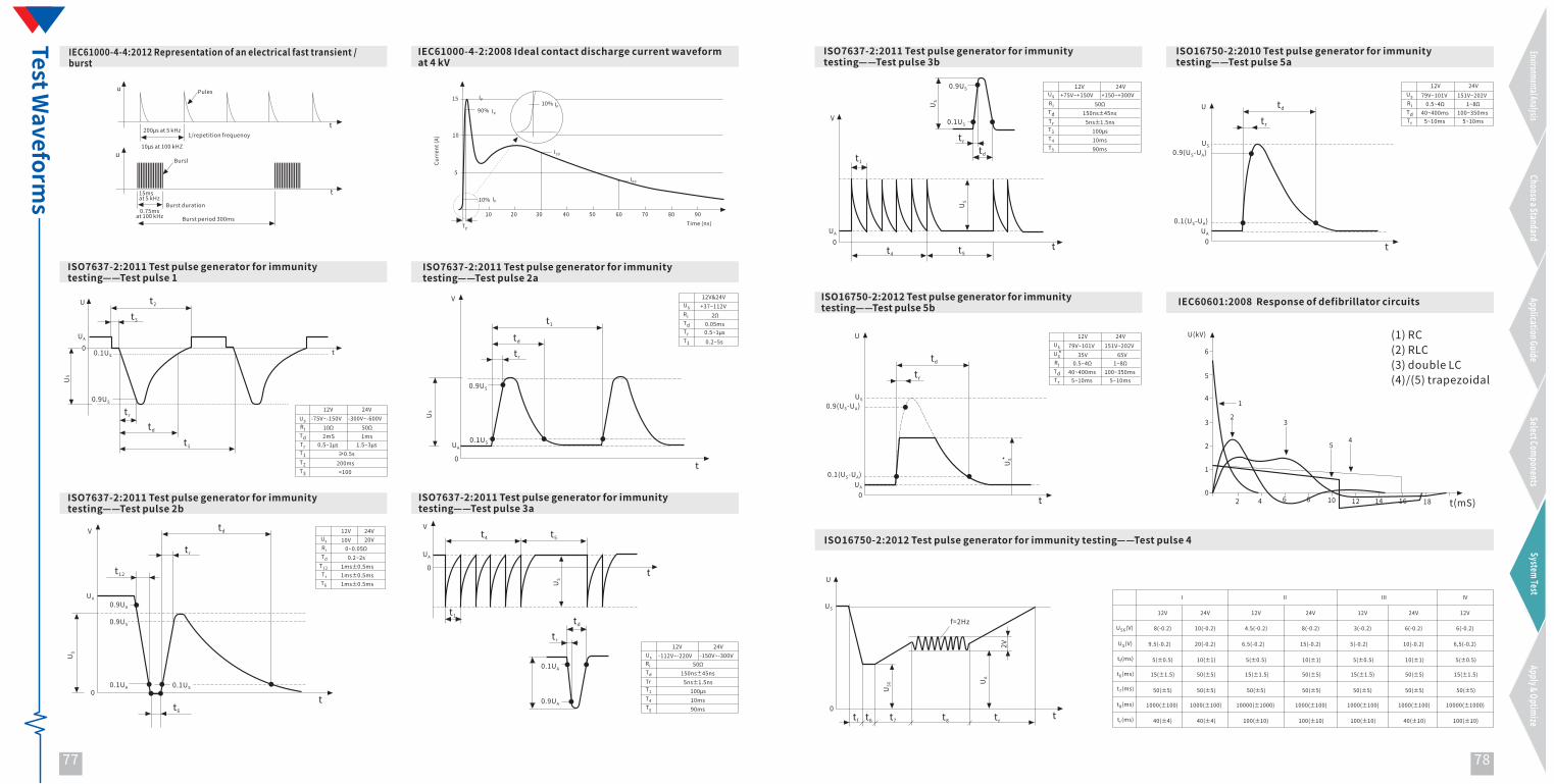
35
UA0
V
t1
t4 t5
US
t
US
0.1US
0.9US
trtd
79V~101V0.5~4Ω�
40~400ms��5~10ms��
12V 24V151V~202V
U
US
0.9(U -U )S A
0.1(U -U )S A
UA0
tdtr
t
U
US
0.9(U -U )S A
0.1(U -U )S A
UA0
tdtr
t
US
U(kV)
t(mS)
2
3
4
5
6
1
02 4 6 8 10 12� 14� 16� 18
1
23
45
(1)�RC�(2)�RLC�(3)�double�LC�(4)/(5)�trapezoidal
IEC60601:2008��Response�of�defibrillator�circuits�ISO16750-2:2012�Test�pulse�generator�for�immunity�testing——Test�pulse�5b
ISO16750-2:2010�Test�pulse�generator�for�immunity�testing——Test�pulse�5a
ISO7637-2:2011�Test�pulse�generator�for�immunity�testing——Test�pulse�3b
12V 24V
50Ω��150ns��±45ns��5ns��±1.5ns��
100μs��10ms��90ms��
T4�T5�
+75V~+150V �+150~+300V�
12V 24V 12V 24V 12V 24V 12V
I� II� III� IV
U (V)���S6 8(-0.2)��� 4.5(-0.2)��� 3(-0.2)��� 6(-0.2)
U (V)���S 9.5(-0.2) � 6.5(-0.2) � 5(-0.2)� 6,5(-0.2)
t (ms) � ��f 5(±0.5)� 5(±0.5)� 5(±0.5) � 5(±0.5)
15(±1.5)� 15(±1.5) � 15(±1.5)� 15(±1.5)
50(±5)� 50(±5)� 50(±5)� 50(±5)
1000(±100)� 10000(±1000)� 1000(±100) 10000(±1000)�
40(±4)� 100(±10)� 100(±10) � 100(±10)
10(-0.2)��� 8(-0.2)��� 6(-0.2)
20(-0.2)��� 15(-0.2)��� 10(-0.2)
10(±1)��� 10(±1)��� 10(±1)
50(±5)��� 50(±5)��� 50(±5)
50(±5)��� 50(±5)��� 50(±5)
1000(±100)��� 1000(±100)��� 1000(±100)
40(±4)��� 100(±10)��� 40(±10)
U
US
0
US6 U
A
2V
f=2Hz
tt7 t8 trt6tf
ISO16750-2:2012�Test�pulse�generator�for�immunity�testing——Test�pulse�4
u Pules
Bursl
t
u
t
200μs�at�5�kHz
10μs�at�100�kHZ
1/repetition�frequenoy
15msat�5�kHz
0.75msat�100�kHz Burst�period�300ms
Burst�duration
IEC61000-4-4:2012�Representation�of�an�electrical�fast�transient�/burst
10 20 30 40 50 60 70 80 90
10% IP
10
15
5
IP
90% IP10% IP
I30
I60
IEC61000-4-2:2008�Ideal�contact�discharge�current�waveform�at�4�kV
Curren
t�(A)
Time�(ns)
U
UA
0
t2
US
0.1US
0.9US
t
V
US
0
V
0.1US
t3
trtd
t1 UA0.1US
0.9US
t1tdtr
t
td
tr
t12
0.9US
0.9UA
tt6
0.1UA
UA
US
0
UA
0
V
t1
t4 t5U
S
t
-75V~-150VUs�Ri�Td�Tr�T1�T2�T3�
10Ω�2mS�
0.5~1μs�
50Ω�1ms�
1.5~3μs�≥0.5s��200ms��<100��
12V 24V-300V~-600V
12V 24V
0.1UA
0.9UA
tdtr
ISO7637-2:2011�Test�pulse�generator�for�immunity�testing——Test�pulse�2b
ISO7637-2:2011�Test�pulse�generator�for�immunity�testing——Test�pulse�1
ISO7637-2:2011�Test�pulse�generator�for�immunity�testing——Test�pulse�2a
ISO7637-2:2011�Test�pulse�generator�for�immunity�testing——Test�pulse�3a
12V&24VUs�Ri�Td�Tr�T1�
+37~112V��2��
0.05ms��0.5~1μs��0.2~5s��
12V 24VUs�Ri�Td�T12�Tr�T6�
0~0.05��0.2~2s��
1ms±0.5ms��1ms±0.5ms��1ms±0.5ms��
10V 20V
U �sR �iT �dTr�T1�T4�T �5
50Ω��150ns��±45ns��5ns��±1.5ns��
100μs��10ms��90ms��
-112V~-220V� -150V~-300V�
Tr
Us�Ri�Td�Tr�T1�
Us�Ri�Td�Tr�
t (ms) � ��6
t (ms) � ��7
t (ms) � ��8
t (ms) � ��r
1~8�100~350ms��5~10ms��
79V~101V
0.5~4�40~400ms��5~10ms��
12V 24V151V~202VUs�
Ri�Td�Tr�
1~8�100~350ms��5~10ms��
Us�* 35V 65V
*
Test�Waveform
s
77� 78�
Environmental�AnalysisChoose�a�Standard
Application�GuideSelect�Components
System�TestApply�&�Optimize

37
ISO9001:2008
OHSAS�18001:2007 ISO14001:2004
C-RoHS
UL-CCIC
Qualification�Certifisate
TS16949:2009
79� 80�
Environmental�AnalysisChoose�a�Standard
Application�GuideSelect�Components
System�TestApply�&�Optimize

51 ±30�
1
Copper�thickness(OZ) Trace�widths@Surface(�mil)Voltage(KV)
83 ±30�
Test�time�s�
104 ±30�
125 ±30�
156 ±30�
54 ±30�2
86 ±30�
Current(KA)
±30�
±30�
±30�
±30�
±30�
±30�
±30�
±30�
Trace�widths�@Surface(�mil) Test�time�s�
0.5�
1�
1.5�
2�
2.5�
3�
3.5�
4�
4.5�
5�5.5�
6�
6.5�
7�
7.5�8�
8.5�9�9.5�
10�
12�
30�
30�
40�
50�
80�
80�
80�
100�
100�120�
120�
200�
200�
200�200�
200�250�250�
250�
20�
40�
60�
80�
100�
100�
140�
180�
180�
200�240�
250�
300�
300�
360�360�
360�360�400�
400�
Trace�widths@Inlayer�(mil)
±30�
±30�
±30�
±30�
±30�
±30�±30�
±30�±30�
±30�
±30�
±30�
X-RAY�perspective�detector Scanning�electron�microscope
Reliability�Lab
RoHS�Tester Film�thickness�tester
37
10/700μs−5/320μs(40Ω)�1KV-6KV
8/20μs��0.5KA-10KA(1OZ)
Temperature�cycle
High-temperature�reverse�bias �High�temperature�and�humidity Highly�accelerated�stress�test
Reliability�Lab�&�Layout�Recom
mended
81� 82�
Layout�Recommended Environmental�AnalysisChoose�a�Standard
Application�GuideSelect�Components
System�TestApply�&�Optimize

MEM
O