gc868-dual hardware user guide -...
TRANSCRIPT

GC868-DUAL Hardware User Guide 1vv0300806 Rev.1 2009-11-17

GC868-DUAL Hardware User Guide 1vv0300806 Rev.1 2009-11-17
Reproduction forbidden without Telit Communications S.p.A’s. written authorization - All Rights Reserved. Page 2 of 47
Disclaimer
The information contained in this document is the proprietary information of Telit Communications S.p.A. and its affiliates (“TELIT”).
The contents are confidential and any disclosure to persons other than the officers, employees, agents or subcontractors of the owner or licensee of this document, without the prior written consent of Telit, is strictly prohibited.
Telit makes every effort to ensure the quality of the information it makes available. Notwithstanding the foregoing, Telit does not make any warranty as to the information contained herein, and does not accept any liability for any injury, loss or damage of any kind incurred by use of or reliance upon the information.
Telit disclaims any and all responsibility for the application of the devices characterized in this document, and notes that the application of the device must comply with the safety standards of the applicable country, and where applicable, with the relevant wiring rules.
Telit reserves the right to make modifications, additions and deletions to this document due to typographical errors, inaccurate information, or improvements to programs and/or equipment at any time and without notice.
Such changes will, nevertheless be incorporated into new editions of this document.
Copyright: Transmittal, reproduction, dissemination and/or editing of this document as well as utilization of its contents and communication thereof to others without express authorization are prohibited. Offenders will be held liable for payment of damages. All rights are reserved.
© 2009 Telit Communications S.p.A.
Printed in the U.S.

GC868-DUAL Hardware User Guide 1vv0300806 Rev.1 2009-11-17
Reproduction forbidden without Telit Communications S.p.A’s. written authorization - All Rights Reserved. Page 3 of 47
Contents 1. INTRODUCTION ..................................................................................................................................................... 5
1.1. CONTACT INFORMATION, SUPPORT...................................................................................................................... 5 1.2. TEXT COVENTIONS .............................................................................................................................................. 6 1.3. RELATED DOCUMENTS ......................................................................................................................................... 6 1.4. TERMS AND ABBREVIATIONS ............................................................................................................................... 7 1.5. DOCUMENT HISTORY......................................................................................................................................... 10
2. PRODUCT CONCEPT ........................................................................................................................................... 11 2.1. GC868-DUAL KEY FEATURES........................................................................................................................... 11
3. APPLICATION INTERFACE ............................................................................................................................... 13 3.1. GC868-DUAL PIN DESCRIPTION....................................................................................................................... 13 3.2. OPERATING MODES ............................................................................................................................................ 16 3.3. POWER SUPPLY .................................................................................................................................................. 16
3.3.1. Power supply pins on the board-to-board connector ................................................................................... 17 3.3.2. Minimizing power losses............................................................................................................................... 17
3.4. POWER UP AND POWER DOWN SCENARIOS ......................................................................................................... 18 3.4.1. Turn on GC868-DUAL ................................................................................................................................. 18
3.4.1.1. Turn on GC868-DUAL using the PWRKEY pin (Power on) ................................................................................18 3.4.1.2. Turn on GC868-DUAL using the RTC (Alarm mode)。 ......................................................................................19
3.4.2. Turn off GC868-DUAL ................................................................................................................................. 19 3.4.2.1. Turn off GC868-DUAL using the PWRKEY pin (Power down)...........................................................................19 3.4.2.2. Under-voltage automatic shutdown........................................................................................................................20
3.4.3. Restart GC868-DUAL using the PWRKEY pin............................................................................................. 20 3.5. POWER SAVING .................................................................................................................................................. 21
3.5.1. Sleep mode (Slow Clocking mode)................................................................................................................ 21 3.5.2. Wake up GC868-DUAL from SLEEP mode.................................................................................................. 21
3.6. RTC BACKUP ..................................................................................................................................................... 22 3.7. SERIAL INTERFACES ........................................................................................................................................... 25
3.7.1. Function of Serial Port ................................................................................................................................. 25 3.8. AUDIO INTERFACE ............................................................................................................................................. 26
3.8.1. Speaker interface configuration.................................................................................................................... 26 3.8.2. Microphone interfaces configuration ........................................................................................................... 27 3.8.3. Referenced Electronic Characteristic........................................................................................................... 27
3.9. SIM CARD INTERFACE........................................................................................................................................ 28 3.9.1. SIM card application .................................................................................................................................... 28 3.9.2. Design considerations for SIM card holder.................................................................................................. 30
3.10. GENERAL PURPOSE INPUT OUTPUT (GPIO)....................................................................................................... 32
4. ANTENNA INTERFACE ....................................................................................................................................... 33 4.1. ANTENNA INSTALLATION................................................................................................................................... 33
4.1.1. Antenna connector ........................................................................................................................................ 33 4.1.2. Antenna pad.................................................................................................................................................. 33
4.2. MODULE RF OUTPUT POWER ............................................................................................................................. 34 4.3. MODULE RF RECEIVE SENSITIVITY .................................................................................................................... 34 4.4. MODULE RECEIVE/TRANSMIT FREQUENCY......................................................................................................... 34 4.5. ANTENNA GAIN.................................................................................................................................................. 34
5. ELECTRICAL, RELIABILITY AND RADIO CHARACTERISTICS ............................................................. 35 5.1. ABSOLUTE MAXIMUM RATINGS.......................................................................................................................... 35
GC868-DUAL Hardware User Guide 1vv0300806 Rev.1 2009-11-17
Reproduction forbidden without Telit Communications S.p.A’s. written authorization - All Rights Reserved. Page 4 of 47
5.2. OPERATING TEMPERATURES .............................................................................................................................. 35 5.3. POWER SUPPLY RATINGS.................................................................................................................................... 36 5.4. CURRENT CONSUMPTION................................................................................................................................... 36 5.5. ELECTROSTATIC DISCHARGE.............................................................................................................................. 37
6. MECHANICS........................................................................................................................................................... 38 6.1. MECHANICAL DIMENSIONS OF GC868-DUAL................................................................................................... 38 6.2. MOUNTING GC868-DUAL ONTO THE APPLICATION PLATFORM ........................................................................ 39 6.3. BOARD-TO-BOARD CONNECTOR......................................................................................................................... 40
6.3.1. Mechanical dimensions of B2B connector.................................................................................................... 40 6.4. RF ADAPTER CABLING....................................................................................................................................... 42 6.5. PIN ASSIGNMENT OF BOARD-TO-BOARD CONNECTOR OF GC868-DUAL .......................................................... 44

GC868-DUAL Hardware User Guide 1vv0300806 Rev.1 2009-11-17
Reproduction forbidden without Telit Communications S.p.A’s. written authorization - All Rights Reserved. Page 5 of 47
1. Introduction This document describes the hardware interface of the Telit GC868-DUAL module that connects to the specific application and the air interface. As GC868-DUAL can be integrated with a wide range of applications, all functional components of GC868-DUAL are described in great detail.
This document can help you to understand GC868-DUAL interface specifications, electrical and mechanical details. With the help of this document and other GC868-DUAL application notes, user guide, you can use GC868-DUAL module to design and set-up mobile applications in a short time.
1.1. Contact Information, Support
For general contact, technical support, to report documentation errors and to order manuals, contact Telit’s Technical Support Center (TTSC) at:
[email protected] [email protected] [email protected] [email protected]
Alternatively, use:
http://www.telit.com/en/products/technical-support-center/contact.php
For detailed information about where you can buy the Telit modules or for recommendations on accessories and components visit:
http://www.telit.com
To register for product news and announcements or for product questions contact Telit's Technical Support Center (TTSC).
Our aim is to make this guide as helpful as possible. Keep us informed of your comments and suggestions for improvements.
Telit appreciates feedback from the users of our information.

GC868-DUAL Hardware User Guide 1vv0300806 Rev.1 2009-11-17
Reproduction forbidden without Telit Communications S.p.A’s. written authorization - All Rights Reserved. Page 6 of 47
1.2. Text Coventions
Danger – This information MUST be followed or catastrophic equipment failure or bodily injury may occur.
Caution or Warning – Alerts the user to important points about integrating the module, if these points are not followed, the module and end user equipment may fail or malfunction.
Tip or Information – Provides advice and suggestions that may be useful when integrating the module.
All dates are in ISO 8601 format, i.e. YYYY-MM-DD.
1.3. Related documents
Table 1:Related documents
SN Document name Remark
[1] ITU-T Draft new recommendation V.25ter:
Serial asynchronous automatic dialing and control
[2] GSM 07.07: Digital cellular telecommunications (Phase 2+); AT command set for GSM Mobile Equipment (ME)
[3] GSM 07.05:
Digital cellular telecommunications (Phase 2+); Use of Data Terminal Equipment – Data Circuit terminating Equipment (DTE – DCE) interface for Short Message Service (SMS) and Cell Broadcast Service (CBS)
[4] GSM 11.14: Digital cellular telecommunications system (Phase 2+); Specification of the SIM Application Toolkit for the Subscriber Identity Module – Mobile Equipment (SIM – ME) interface
[5] GSM 11.11: Digital cellular telecommunications system (Phase 2+); Specification of the Subscriber Identity Module – Mobile Equipment (SIM – ME) interface
[6] GSM 03.38: Digital cellular telecommunications system (Phase 2+); Alphabets and language-specific information
[7] GSM 11.10 Digital cellular telecommunications system (Phase 2); Mobile Station

GC868-DUAL Hardware User Guide 1vv0300806 Rev.1 2009-11-17
Reproduction forbidden without Telit Communications S.p.A’s. written authorization - All Rights Reserved. Page 7 of 47
(MS) conformance specification; Part 1: Conformance specification
1.4. Terms and abbreviations
Table 2:Terms and abbreviations Abbreviation Description
ADC Analog-to-Digital Converter
ARP Antenna Reference Point
ASIC Application Specific Integrated Circuit
BER Bit Error Rate
BTS Base Transceiver Station
CHAP Challenge Handshake Authentication Protocol
CS Coding Scheme
CSD Circuit Switched Data
CTS Clear to Send
DAC Digital-to-Analog Converter
DRX Discontinuous Reception
DSP Digital Signal Processor
DTE Data Terminal Equipment (typically computer, terminal, printer)
DTR Data Terminal Ready
DTX Discontinuous Transmission
EFR Enhanced Full Rate
EGSM Enhanced GSM
EMC Electromagnetic Compatibility
ESD Electrostatic Discharge
ETS European Telecommunication Standard
FCC Federal Communications Commission (U.S.)
FDMA Frequency Division Multiple Access
FR Full Rate
GMSK Gaussian Minimum Shift Keying

GC868-DUAL Hardware User Guide 1vv0300806 Rev.1 2009-11-17
Reproduction forbidden without Telit Communications S.p.A’s. written authorization - All Rights Reserved. Page 8 of 47
GPRS General Packet Radio Service
GSM Global Standard for Mobile Communications
Abbreviation Description
HR Half Rate
I/O Input/Output
IC Integrated Circuit
IMEI International Mobile Equipment Identity
Inorm Normal Current
Imax Maximum Load Current
kbps Kilo bits per second
LED Light Emitting Diode
Li-Ion Lithium-Ion
MO Mobile Originated
MS Mobile Station (GSM engine), also referred to as TE
MT Mobile Terminated
PAP Password Authentication Protocol
PBCCH Packet Switched Broadcast Control Channel
PCB Printed Circuit Board
PCS Personal Communication System, also referred to as GSM 1900
PDU Protocol Data Unit
PPP Point-to-point protocol
RF Radio Frequency
RMS Root Mean Square (value)
RTC Real Time Clock
Rx Receive Direction
SIM Subscriber Identification Module
SMS Short Message Service
TDMA Time Division Multiple Access
TE Terminal Equipment, also referred to as DTE
TX Transmit Direction

GC868-DUAL Hardware User Guide 1vv0300806 Rev.1 2009-11-17
Reproduction forbidden without Telit Communications S.p.A’s. written authorization - All Rights Reserved. Page 9 of 47
UART Universal Asynchronous Receiver & Transmitter
URC Unsolicited Result Code
Abbreviation Description
USSD Unstructured Supplementary Service Data
VSWR Voltage Standing Wave Ratio
Vmax Maximum Voltage Value
Vnorm Normal Voltage Value
Vmin Minimum Voltage Value
VIHmax Maximum Input High Level Voltage Value
VIHmin Minimum Input High Level Voltage Value
VILmax Maximum Input Low Level Voltage Value
VILmin Minimum Input Low Level Voltage Value
VImax Absolute Maximum Input Voltage Value
VImin Absolute Minimum Input Voltage Value
VOHmax Maximum Output High Level Voltage Value
VOHmin Minimum Output High Level Voltage Value
VOLmax Maximum Output Low Level Voltage Value
VOLmin Minimum Output Low Level Voltage Value
Phonebook abbreviations
Abbreviation Description
FD SIM fix dialing phonebook
LD SIM last dialing phonebook (list of numbers most recently dialed)
MC Mobile Equipment list of unanswered MT calls (missed calls)
ON SIM (or ME) own numbers (MSISDNs) list
RC Mobile Equipment list of received calls
SM SIM phonebook
GC868-DUAL Hardware User Guide 1vv0300806 Rev.1 2009-11-17
Reproduction forbidden without Telit Communications S.p.A’s. written authorization - All Rights Reserved. Page 10 of 47
1.5. Document History
Revision Date Changes
1 2009-11-17 Updated on temperature range and IO descriptions
Changed on B2B connector selection
0 2009-10-12: First issue

GC868-DUAL Hardware User Guide 1vv0300806 Rev.1 2009-11-17
Reproduction forbidden without Telit Communications S.p.A’s. written authorization - All Rights Reserved. Page 11 of 47
2. Product concept Designed for global market, GC868-DUAL is a Dual-band GSM engine that can work on frequencies EGSM900 MHz/DCS1800 MHz , it supports by default a low/high pair of bands at the same time.
With a tiny configuration of 35mm x 32mm x 3.1 mm , GC868-DUAL was developed for very low cost voice-only GSM system solutions.
The physical interface to the mobile application is made through a 60 pins board-to-board connector, which provides all hardware interfaces between the module and customers’ boards except the RF antenna interface.
• One serial port can help you easily develop your applications.
• Two audio channels include two microphones inputs and two speaker outputs. This can be easily configured by AT command.
GC868-DUAL provide RF antenna interface with two alternatives: antenna connector and antenna pad. The antenna connector is MURATA MM9329-2700, or customer’s antenna can be soldered to the antenna pad.
The GC868-DUAL is designed with power saving technique, the average current consumption is as low as 2.9mA in SLEEP mode.
2.1. GC868-DUAL key features
Table 3:GC868-DUAL key features
Feature Implementation
Power supply Single supply voltage 3.4V – 4.5V
Power saving Typical power consumption in SLEEP mode to 2.9mA
Frequency bands
GC868-DUAL Dual-band: EGSM 900/DCS 1800
Compliant to GSM Phase 2/2+
GSM class Small MS
Transmit power Class 4 (2W) at EGSM900
Class 1 (1W) at DCS1800
Temperature range
Normal operation: -20°C to +55°C
Restricted operation: -30°C to -20°C and +55°C to +80°C
Storage temperature -40°C to +85°C

GC868-DUAL Hardware User Guide 1vv0300806 Rev.1 2009-11-17
Reproduction forbidden without Telit Communications S.p.A’s. written authorization - All Rights Reserved. Page 12 of 47
CSD: CSD transmission rates: 2.4, 4.8, 9.6, 14.4 kbps, non-transparent
Unstructured Supplementary Services Data (USSD) support
SMS
MT, MO, CB, Text and PDU mode
SMS storage: SIM card
Support transmission of SMS alternatively over CSD . User can choose preferred mode.
SIM interface Supported SIM card: 1.8V, 3V
External antenna Connected via 50 Ohm antenna connector
Audio features
Speech codec modes:
Half Rate (ETS 06.20)
Full Rate (ETS 06.10)
Enhanced Full Rate (ETS 06.50 / 06.60 / 06.80)
AMR
Echo suppression
One serial interface
Serial Port 1 Seven lines on Serial Port Interface
Serial Port 1 can be used for CSD FAX, and send AT command of controlling module.
Phonebook management Supported phonebook types: SM, FD, LD, RC, ON, MC.
SIM Application Toolkit Supports SAT class 3, GSM 11.11 phase 2+ standard
Real time clock Implemented
Timer function Programmable via AT command
Physical characteristics
Size: 35±0.15 x 32±0.15 x 3.3±0.3 mm (including application connector)
35±0.15 x 32±0.15 x 2.85±0.3 mm (excluding application connector)
Weight: 8g
Firmware upgrade Firmware upgradeable over serial interface

GC868-DUAL Hardware User Guide 1vv0300806 Rev.1 2009-11-17
Reproduction forbidden without Telit Communications S.p.A’s. written authorization - All Rights Reserved. Page 13 of 47
3. Application Interface All hardware interfaces, except for RF interface that connects GC868-DUAL to the customers’ cellular application platform, go through a 60-pin 0.5mm pitch board-to-board connector.
Sub-interfaces included in this board-to-board connector are described in detail in following chapters:
• Power supply (see Chapters 3.3)
• One serial interface (see Chapter 3.7)
• Two analog audio interfaces (see Chapter 3.8)
• SIM interface (see Chapter 3.9)
Mechanical characteristics of the board-to-board connector are specified in Chapter 6.3. There is also descrived the information of mating connector.
3.1. GC868-DUAL Pin description
Table 4:Board-to-Board Connector pin description Power Supply
PIN NAME I/O DESCRIPTION DC CHARACTERISTICS
VBAT P Eight BAT pins of the board-to-board connector are dedicated to connect the supply voltage. The power supply of GC868-DUAL has to be a single voltage source of VBAT= 3.4V...4.5V. It must be able to provide sufficient current in a transmit burst which typically rises to 2A.mostly, these 8 pins are voltage input
Vmax= 4.5V
Vmin=3.4V
Vnorm=4.0V
VRTC P Current input for RTC when the battery is not supplied for the system.
Current output for backup battery when the main battery is present and the backup battery in low voltage state.
Vmax=2.14V
Vmin=1.86V
Vnorm=2.0V
I max=13mA
I min=0.5mA

GC868-DUAL Hardware User Guide 1vv0300806 Rev.1 2009-11-17
Reproduction forbidden without Telit Communications S.p.A’s. written authorization - All Rights Reserved. Page 14 of 47
VDD_EXT P Supply 2.85V voltage for external circuit. By measure this pin, user can judge the system is on or off.
When the voltage is low, the system is off. Otherwise, the system is on.
Vmax=2.95V
Vmin=2.75V
Vnorm=2.85V
Imax=20mA
GND G Digital ground
Power on or power off
PIN NAME I/O DESCRIPTION
PWRKEY I Voltage input for power on key. ON/OFF get a high level Voltage as VRTC for user to power on or power off the system. The user should keep pressing the key for a moment when power on or power off the system. Because the system need margin time assert the software.
Audio interfaces
PIN NAME I/O DESCRIPTION
MIC1P
MIC1N
I Positive and negative voice-band input
MIC2P
MIC2N
I Auxiliary positive and negative voice-band input
SPK1P
SPK1N
O Positive and negative voice-band output
SPK2P
SPK2N
O Auxiliary Positive and negative voice-band output
GERNERAL PURPOSE input/output
PIN NAME I/O DESCRIPTION
GPIO1 I/O
GPIO2 I/O
GPIO3 I/O
GPIO4 I/O
GPIO5 I/O
The GPO can be configured by AT command for outputting high or low level voltage. All of the GPIOs are initial low without any setting from AT command.

GC868-DUAL Hardware User Guide 1vv0300806 Rev.1 2009-11-17
Reproduction forbidden without Telit Communications S.p.A’s. written authorization - All Rights Reserved. Page 15 of 47
GPIO6 I/O
GPIO7 I/O
GPIO8 I/O
Serial interface
PIN NAME I/O DESCRIPTION
RXD I Receive Data
TXD O Transmit Data
RTS I Request to Send
CTS O Clear to Send
DCD O Data Carrier Detect
DSR O Data Set Ready
DTR I Data Terminal Ready
RING O Ring Indicator(RI)
SIM interface
PIN NAME I/O DESCRIPTION
SIM_VDD O Voltage Supply for SIM card
SIM_I/O I/O SIM Data Input/Output
SIM_CLK O SIM Clock
SIM_RST O SIM Reset

GC868-DUAL Hardware User Guide 1vv0300806 Rev.1 2009-11-17
Reproduction forbidden without Telit Communications S.p.A’s. written authorization - All Rights Reserved. Page 16 of 47
3.2. Operating modes
The following table summarizes the various operating modes:
Table 5:Overview of operating modes
3.3. Power supply
The power supply of GC868-DUAL is from a single voltage source of VBAT= 3.4V...4.5V. In some case, the ripple in a transmit burst may cause voltage drops when current consumption rises to typical peaks of 2A. Therefore the power supply must be able to provide sufficient current up to 2A.
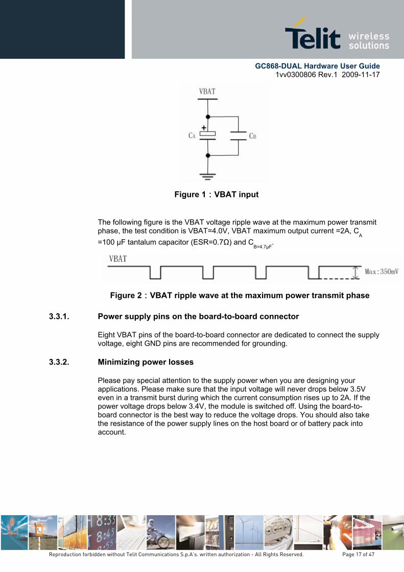
For the VBAT input, a local bypass capacitor is recommended. A capacitor about 100µF, low ESR is recommended. Multi-layer Ceramic Chip (MLCC) capacitors can provide the best combination of low ESR and small size but are not cost effective. A lower cost choice may be a 100 µF tantalum capacitor (low ESR) with a small (1 µF to 10µF) ceramic in parallel, which is illustrated as following figure. And the capacitors should put as closer as possible to the GC868-DUAL VBAT pins. The following figure is the recommended circuit.
Mode Function
GSM SLEEP
Module will automatically go into SLEEP mode if there is no on air or audio activity is required and no hardware interrupt (such as GPIO interrupt or data on serial port).
In this case, the current consumption of module will reduce to the minimal level.
During sleep mode, the module can still receive paging message and SMS from the system normally.
GSM IDLE Software is active. Module has registered to the GSM network, and the module is ready to send and receive.
Normal operation
GSM TALK
CSD connection is going on between two subscribers. In this case, the power consumption depends on network settings such as DTX off/on, FR/EFR/HR, hopping sequences, antenna.
Alarm mode RTC alert function launches this restricted operation while the module is in POWER DOWN mode. GC868-DUAL will not be registered to GSM network and only parts of AT commands can be available.
GC868-DUAL Hardware User Guide 1vv0300806 Rev.1 2009-11-17
Reproduction forbidden without Telit Communications S.p.A’s. written authorization - All Rights Reserved. Page 17 of 47
Figure 1:VBAT input
The following figure is the VBAT voltage ripple wave at the maximum power transmit phase, the test condition is VBAT=4.0V, VBAT maximum output current =2A, C
A
=100 µF tantalum capacitor (ESR=0.7Ω) and CB=4.7µF
.
Figure 2:VBAT ripple wave at the maximum power transmit phase
3.3.1. Power supply pins on the board-to-board connector
Eight VBAT pins of the board-to-board connector are dedicated to connect the supply voltage, eight GND pins are recommended for grounding.
3.3.2. Minimizing power losses
Please pay special attention to the supply power when you are designing your applications. Please make sure that the input voltage will never drops below 3.5V even in a transmit burst during which the current consumption rises up to 2A. If the power voltage drops below 3.4V, the module is switched off. Using the board-to-board connector is the best way to reduce the voltage drops. You should also take the resistance of the power supply lines on the host board or of battery pack into account.

GC868-DUAL Hardware User Guide 1vv0300806 Rev.1 2009-11-17
Reproduction forbidden without Telit Communications S.p.A’s. written authorization - All Rights Reserved. Page 18 of 47
3.4. Power up and power down scenarios
3.4.1. Turn on GC868-DUAL
GC868-DUAL can be turned on by various ways, which are described in following chapters:
Via PWRKEY pin: starts normal operating mode (see chapter 3.4.1.1);
Via RTC interrupt: starts ALARM modes (see chapter 3.4.1.2)
3.4.1.1. Turn on GC868-DUAL using the PWRKEY pin (Power on) You can turn on the GC868-DUAL by driving the PWRKEY to a high level voltage for period time. The power on scenarios illustrate as following figure.
Figure 3:Timing of turn on system
When power on procedure has completed, GC868-DUAL sends out the following result code to indicate the module is ready to operate:
RDY
NOTE: Only enter AT command through serial port after GC868-DUAL is power on and Unsolicited Result Code “RDY” is received from serial port.

GC868-DUAL Hardware User Guide 1vv0300806 Rev.1 2009-11-17
Reproduction forbidden without Telit Communications S.p.A’s. written authorization - All Rights Reserved. Page 19 of 47
3.4.1.2. Turn on GC868-DUAL using the RTC (Alarm mode)。
Alarm mode is a power-on approach by using the RTC.The alert function of RTC makes the GC868-DUAL wake up while the module is power off. In alarm mode, GC868-DUAL does not register to GSM network and the software protocol stack is close. Thus, the parts of AT commands related to SIM card and Protocol stack are not accessible, and the others can be used as well as in normal mode.
3.4.2. Turn off GC868-DUAL
Following procedure can be used to turn off the GC868-DUAL:
• Normal power down procedure: Turn off GC868-DUAL using the PWRKEY pin
• Normal power down procedure: Turn off GC868-DUAL using AT command
• Under-voltage automatic shutdown: Takes effect if Under-voltage is detected
3.4.2.1. Turn off GC868-DUAL using the PWRKEY pin (Power down) You can turn off the GC868-DUAL by driving the PWRKEY to a high level voltage for a period of time. The power down scenarios are illustrated in the following Figure.
This procedure lets the module log off from the network and allow the software entering into a secure state and save data before completely disconnect the power supply.
Before the completion of the switching off procedure, the module sends out result code:
POWER DOWN
After this moment, no any AT commands can be executed. Module enters the POWER DOWN mode, only the RTC is still active. POWER DOWN can also be indicated by VDD_EXT pin, which is a low level voltage in this mode.

GC868-DUAL Hardware User Guide 1vv0300806 Rev.1 2009-11-17
Reproduction forbidden without Telit Communications S.p.A’s. written authorization - All Rights Reserved. Page 20 of 47
ON/~OFF INPUT
VDD_EXT(OUTPUT)
Vic<0.3*VRTCHiz
1000ms>shut>500ms
Logout net about 2000 to 5000ms
Vih>0.7*VRTC
Figure 4:Timing of turn off system
3.4.2.2. Under-voltage automatic shutdown Software constantly monitors the voltage level applied on the VBAT, if the measured battery voltage does not exceed 3.4V, the following URC is presented:
POWER LOW WARNNING
If the measured battery voltage does not exceed 3.4V, the following URC is presented:
POWER LOW DOWN
After this moment AT commands can be executed. The module will log off from the network and enters POWER DOWN mode, only the RTC is still active. POWER DOWN can also be indicated by VDD_EXT pin, which is a low level voltage in this mode.
3.4.3. Restart GC868-DUAL using the PWRKEY pin
You can restart GC868-DUAL by driving the PWRKEY to a high level voltage for a time period, the same as turning on GC868-DUAL using the PWRKEY pin. Before restarting the GC868-DUAL, you need to wait at least 500ms after detecting the VDD_EXT low level on. The restart scenarios are illustrated in the following figure.

GC868-DUAL Hardware User Guide 1vv0300806 Rev.1 2009-11-17
Reproduction forbidden without Telit Communications S.p.A’s. written authorization - All Rights Reserved. Page 21 of 47
ON/~OFF INPUT
VDD_EXT(OUTPUT)
Vic<0.3*VRTC
Hiz
Turn offRestart>500
ms
Figure 5:Timing of restart system
3.5. Power saving
3.5.1. Sleep mode (Slow Clocking mode)
When there is no on air or audio activity is required and no hardware interrupt (such as GPIO interrupt or data on serial port), GC868-DUAL enters into SLEEP mode automatically. In this mode, GC868-DUAL can still receive paging or SMS from network.
In SLEEP mode, the serial port is not accessible.
3.5.2. Wake up GC868-DUAL from SLEEP mode
When GC868-DUAL is in SLEEP mode, the following method can wake up the module.
• Receive a voice or data call from the network to wake up GC868-DUAL;
• Receive an SMS from the network to wake up GC868-DUAL
• RTC alarm expired to wake up GC868-DUAL;

GC868-DUAL Hardware User Guide 1vv0300806 Rev.1 2009-11-17
Reproduction forbidden without Telit Communications S.p.A’s. written authorization - All Rights Reserved. Page 22 of 47
3.6. RTC backup
The Real Time Clock (RTC) power supply of module can be provided by an external battery or a battery (rechargeable or non-chargeable) through PIN 15 on the board-to-board connector. You need only a coin-cell battery or a super-cap to PIN 15 to backup power supply for RTC.
The following figures show various sample circuits for RTC backup.
Figure 6:RTC supply from non-chargeable battery
Figure 7:RTC supply from rechargeable battery
Figure 8:RTC supply from capacitor
Li-battery backup
Rechargeable Lithium coin cells such as the TC614 from Maxell, or the TS621 from Seiko, are also small in size, but have higher capacity than the double layer capacitors resulting in longer backup times.
Typical charge curves for each cell type are shown in the following figures. Note that the rechargeable Lithium type coin cells generally come pre-charged from the vendor.

GC868-DUAL Hardware User Guide 1vv0300806 Rev.1 2009-11-17
Reproduction forbidden without Telit Communications S.p.A’s. written authorization - All Rights Reserved. Page 23 of 47
Figure 9:Panasonic EECEMOE204A Charge Characteristic
Figure 10:Maxell TC614 Charge Characteristic

GC868-DUAL Hardware User Guide 1vv0300806 Rev.1 2009-11-17
Reproduction forbidden without Telit Communications S.p.A’s. written authorization - All Rights Reserved. Page 24 of 47
Figure 11:Seiko TS621 Charge Characteristic
NOTE: Gold-capacitance backup:
Some suitable coin cells are the electric double layer capacitors available from Seiko (XC621), or from Panasonic (EECEM0E204A). They have a small physical size (6.8 mm diameter) and a nominal capacity of 0.2 F to 0.3 F, giving hours of backup time.

GC868-DUAL Hardware User Guide 1vv0300806 Rev.1 2009-11-17
Reproduction forbidden without Telit Communications S.p.A’s. written authorization - All Rights Reserved. Page 25 of 47
3.7. Serial interfaces
GC868-DUAL provides one serial ports. The GSM module is designed as a DCE (Data Communication Equipment), following the traditional DCE-DTE (Data Terminal Equipment) connection, the module and the client (DTE) are connected through the following signal (as following figure shows).
Serial port
• Port/TXD @ Client sends data to the RXD signal line of module
• Port/RXD @ Client receives data from the TXD signal line of module
All pins of serial ports have 8mA driver, the logic levels are described in the following table
Table 6: Logic levels of serial ports pins Parameter Min Max Unit
Logic low input 0 0.3*VDD_EXT V
Logic high input 0.7 *VDD_EXT VDD_EXT +0.3 V
Logic low output GND 0.2 V
Logic high output VDD_EXT -0.2 VDD_EXT V
Figure 12:Interface of serial ports
3.7.1. Function of Serial Port
Serial port
• Four lines on Serial Port Interface
• Contains Data lines /TXD and /RXD, State lines /RTS and /CTS;
• Serial Port can be used for CSD FAX, and send AT command of controlling module; Port can use multiplexing function;
• Serial port supports the communication rate as following: 1200, 2400, 4800, 9600, 19200, 38400, 57600, 115200
Default is 115200bps.

GC868-DUAL Hardware User Guide 1vv0300806 Rev.1 2009-11-17
Reproduction forbidden without Telit Communications S.p.A’s. written authorization - All Rights Reserved. Page 26 of 47
3.8. Audio interface
Table 7:Audio interface signal
The module provides two Analogy input channels, AIN1 and AIN2, which may be used for both microphone and line inputs. The AIN1 and AIN2 channels are identical. One of the two channels is typically used with a microphone built into a handset. The other channel is typically used with an external microphone or external line input. The Module Analogy input configuration is determined by control register settings and established using Analogy multiplexes.
It is suggested that you adopt one of the following two matching circuits in order to satisfy speaker effect. The difference audio signals have to be layout according to different signal layout rules. If you want to adopt an amplifier circuit for audio, we commend National semiconductor’s LM4890. But you can select it according to your needs.
3.8.1. Speaker interface configuration
Figure 13:Speaker interface with amplifier configuration
Name Pin Function
MIC1P 53 Microphone1 input +
MIC1N 55 Microphone1 input -
SPK1P 54 Audio1 output+
(AIN1/AOUT1)
SPK1N 56 Audio1 output-
MIC2P 57 Microphone2 input +
MIC2N 59 Microphone2 input -
SPK2P 58 Audio2 output+
(AIN2/AOUT2)
SPK2N 60 Audio2 output-
GC868-DUAL Hardware User Guide 1vv0300806 Rev.1 2009-11-17
Reproduction forbidden without Telit Communications S.p.A’s. written authorization - All Rights Reserved. Page 27 of 47
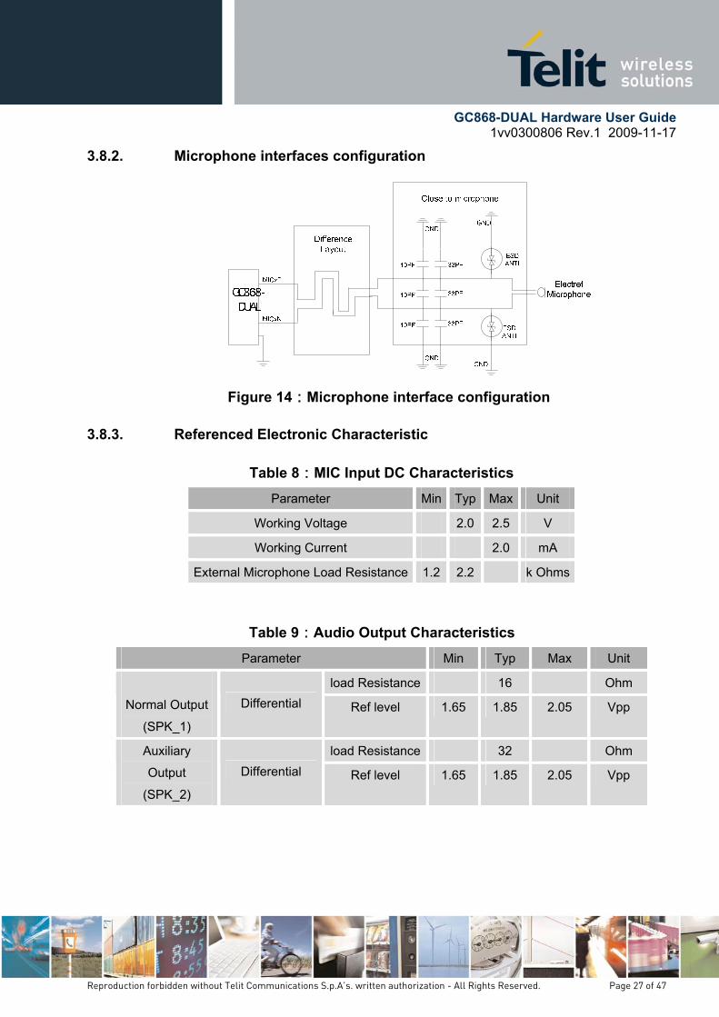
3.8.2. Microphone interfaces configuration
Figure 14:Microphone interface configuration
3.8.3. Referenced Electronic Characteristic
Table 8:MIC Input DC Characteristics
Parameter Min Typ Max Unit
Working Voltage 2.0 2.5 V
Working Current 2.0 mA
External Microphone Load Resistance 1.2 2.2 k Ohms
Table 9:Audio Output Characteristics
Parameter Min Typ Max Unit
load Resistance 16 Ohm
Normal Output
(SPK_1)
Differential Ref level 1.65 1.85 2.05 Vpp
load Resistance 32 Ohm Auxiliary
Output
(SPK_2)
Differential Ref level 1.65 1.85 2.05 Vpp

GC868-DUAL Hardware User Guide 1vv0300806 Rev.1 2009-11-17
Reproduction forbidden without Telit Communications S.p.A’s. written authorization - All Rights Reserved. Page 28 of 47
3.9. SIM card interface
3.9.1. SIM card application
You can use AT Command to get information about the SIM card. For more information, see [1].
The SIM interface supports the functionality of the GSM Phase 1 specification and also supports the functionality of the new GSM Phase 2+ specification for FAST 64 kbps SIM (intended for use with a SIM application Tool-kit). Both 1.8V and 3.0V SIM Cards are supported.
The SIM interface is powered by an internal regulator in the module having 2.8V nominal voltage. All pins reset as outputs driving low. Logic levels are described in the table below:
Table 10:Signal of SIM interface (board-to-board connector) Pin Signal Description
19 SIM_VDD SIM Card Power output automatic output on SIM mode,
one is 3.0V±10%, another is 1.8V±10%. Current is about 10mA.
21 SIM_I/O SIM Card data I/O
23 SIM_CLK SIM Card Clock
25 SIM_RST SIM Card Reset
Following is a reference circuit about SIM interface. We recommend an Electrostatic discharge device ST (www.st.com) ESDA6V1W5 or ON SEMI (www.onsemi.com) SMF05C for “ESD ANTI”.

GC868-DUAL Hardware User Guide 1vv0300806 Rev.1 2009-11-17
Reproduction forbidden without Telit Communications S.p.A’s. written authorization - All Rights Reserved. Page 29 of 47
Figure 15:SIM interface reference circuit with 6pin SIM card
Figure 16:SIM interface reference circuit with 8pin SIM card

GC868-DUAL Hardware User Guide 1vv0300806 Rev.1 2009-11-17
Reproduction forbidden without Telit Communications S.p.A’s. written authorization - All Rights Reserved. Page 30 of 47
3.9.2. Design considerations for SIM card holder
For 6 pin SIM card, we recommend to use Amphenol C707 10M006 049 2. For more information about the holder, see http://www.amphenol.com
Figure 17:Amphenol C707 10M006 049 2 SIM card holder Table 11:Pin description (Amphenol SIM card holder)
Pin Signal Description
C1 SIM_VDD SIM Card Power supply, it can identify automatically the SIM Card power mode,one
is 3.0V±10%, another is 1.8V±10%. Current is about 10mA.
C2 SIM_RST SIM Card Reset.
C3 SIM_CLK SIM Card Clock.
C5 GND Connect to GND.
C6 VPP Not connect.
C7 SIM_I/O SIM Card data I/O.
For 8 pin SIM card, we recommend to use Molex 91128. For more information about the holder, see http://www.molex.com.

GC868-DUAL Hardware User Guide 1vv0300806 Rev.1 2009-11-17
Reproduction forbidden without Telit Communications S.p.A’s. written authorization - All Rights Reserved. Page 31 of 47
Figure 18:Molex 91128 SIM card holder
Table 12:Pin description (Molex SIM card holder) Pin Signal Description
C1 SIM_VDD SIM Card Power supply, it can identify automatically the SIM Card power
mode,one is 3.0V±10%, another is 1.8V±10%. Current is about 10mA.
C2 SIM_RST SIM Card Reset.
C3 SIM_CLK SIM Card Clock.
C4 GND Connect to GND.
C5 GND Connect to GND.
C6 VPP Not connect.
C7 SIM_I/O SIM Card data I/O.

GC868-DUAL Hardware User Guide 1vv0300806 Rev.1 2009-11-17
Reproduction forbidden without Telit Communications S.p.A’s. written authorization - All Rights Reserved. Page 32 of 47
3.10. General Purpose Input Output (GPIO)
GC868-DUAL provides a limited number of General Purpose Input/Output signal pins
Table 13:GPIO Pins of GC868-DUAL Pin Name Type Function
29 GPIO1 I/O General Purpose Input/Output Port
37 GPIO2 I/O General Purpose Input/Output Port
39 GPIO3 I/O General Purpose Input/Output Port
41 GPIO4 I/O General Purpose Input/Output Port
45 GPIO5 I/O General Purpose Input/Output Port
35 GPIO6 I/O General Purpose Input/Output Port
32 GPIO7 I/O General Purpose Input/Output Port
36 GPIO8 I/O General Purpose Input/Output Port

GC868-DUAL Hardware User Guide 1vv0300806 Rev.1 2009-11-17
Reproduction forbidden without Telit Communications S.p.A’s. written authorization - All Rights Reserved. Page 33 of 47
4. Antenna interface The RF interface has an impedance of 50Ω. To suit the physical design of individual applications GC868-DUAL offers two alternatives:
• Recommended approach: antenna connector in the component side of the PCB
• Antenna pad and grounding plane placed at the bottom.
To minimize the loss on the RF cable, the insertion loss should meet the following requirements:
• EGSM900<1dB
• DCS1800<1.5dB
4.1. Antenna installation
4.1.1. Antenna connector
GC868-DUAL uses MURATA’s MM9329-2700 RF connector in the module side. The user should use MURATA’s MXTK as a matching connector on the application side. For more information about MURATA’s MXTK, see the 6.4 RF Adapter cabling.
4.1.2. Antenna pad
The antenna can be soldered to the pad, or attached via contact springs. To help you with grounding the antenna, GC868-DUAL comes with a grounding plane located close to the antenna pad.
GC868-DUAL material properties:
• GC868-DUAL PCB Material: FR4
• Antenna pad: Gold plated pad
Antenna pad soldering temperature (less than 10 seconds): 260°C

GC868-DUAL Hardware User Guide 1vv0300806 Rev.1 2009-11-17
Reproduction forbidden without Telit Communications S.p.A’s. written authorization - All Rights Reserved. Page 34 of 47
4.2. Module RF output power
Table 14:GC868-DUAL RF output power Frequency Max Min
EGSM900 33dBm ±2db 5dBm ±5db
DCS1800 30dBm ±2db 0dBm±5db
4.3. Module RF receive sensitivity
Table 15:GC868-DUAL RF receive sensitivity Frequency Receive sensitivity
EGSM900 < -108dBm
DCS1800 < -107dBm
4.4. Module receive/transmit frequency
Table 16:GC868-DUAL receive/transmit frequency Mode Freq. TX (MHz) Freq. RX (MHz) Channels (ARFC) TX - RX offset
890.0 - 914.8 935.0 - 959.8 0 – 124 45 MHz E-GSM-900
880.2 - 889.8 925.2 - 934.8 975 - 1023 45 MHz
DCS-1800 1710.2 - 1784.8 1805.2 - 1879.8 512 – 885 95 MHz
4.5. Antenna gain
Table 17:Antenna gain Item Parameter
EGSM900 DCS1800 Gain(dBi)
0.5 1
Pattern Omni-directional antenna

GC868-DUAL Hardware User Guide 1vv0300806 Rev.1 2009-11-17
Reproduction forbidden without Telit Communications S.p.A’s. written authorization - All Rights Reserved. Page 35 of 47
5. Electrical, reliability and radio characteristics 5.1. Absolute maximum ratings
Absolute maximum rating for power supply and voltage on digital and analog pins of GC868-DUAL are listed in the following table:
Table 18:Absolute maximum ratings Parameter Min Max Unit
Peak current of power supply 0 4.0 A
RMS current of power supply (during one TDMA- frame) 0 0.7 A
Voltage at digital pins -0.3 3.3 V
Voltage at analog pins -0.3 3.0 V
Voltage at digital/analog pins in POWER DOWN mode -0.25 0.25 V
5.2. Operating temperatures
The operating temperature is listed in the following table:
Table 19:GC868-DUAL operating temperature Parameter Min Typ Max Unit
Ambient temperature -20 +25 +55
Restricted operation* -20 to -30 +55 to +80
Storage temperature -40 +85
* GC868-DUAL is fully functional, but a deviation than GSM specification may be occurred.

GC868-DUAL Hardware User Guide 1vv0300806 Rev.1 2009-11-17
Reproduction forbidden without Telit Communications S.p.A’s. written authorization - All Rights Reserved. Page 36 of 47
5.3. Power supply ratings
Table 20:GC868-DUAL power supply ratings Description Conditions Min Typ Max Unit
Supply voltage Voltage must stay within the min/max values, including voltage drop, ripple, and spikes.
3.4 4.0 4.5 V
Voltage drop during transmit burst
Normal condition, power control level for Pout max
400 mV
Voltage ripple
Normal condition, power control level for Pout max
@ f<200kHz
@ f>200kHz
50
2 mV
5.4. Current Consumption
Table 21:GC868-DUAL current consumption Description Conditions Min Typ Max Unit
POWER DOWN mode
SLEEP mode
35
2.9
uA
mA
IDLE mode
EGSM 900
GSM 1800
23
23
mA Average supply current
TALK mode
EGSM 900
GSM 1800
240
200
mA
Peak supply current (during transmission slot every 4.6ms)
Power control level 2 3 A

GC868-DUAL Hardware User Guide 1vv0300806 Rev.1 2009-11-17
Reproduction forbidden without Telit Communications S.p.A’s. written authorization - All Rights Reserved. Page 37 of 47
5.5. Electrostatic discharge
Normally the module is designed inside customer terminal, so about Electrostatic Discharge (ESD) should be considered based on the terminal product requirements. The module is protected against Electrostatic Discharge in conveyance and customer production, and some second level ESD protection is designed inside the module.
The remaining ports are not equipped with special ESD protection in the module, and they are only protected according to the Human Body Model requirements.
Table 22:The ESD endure statue measured table
(Temperature: 25, Humidity: 45% )
Part Contact discharge Air discharge
VBAT,GND ±2KV ±4KV
DTR, RXD, TXD, RTS ±1KV ±2KV
Antenna port ±1KV ±2KV
Other port ±1KV ±2KV
GC868-DUAL Hardware User Guide 1vv0300806 Rev.1 2009-11-17
Reproduction forbidden without Telit Communications S.p.A’s. written authorization - All Rights Reserved. Page 38 of 47
6. Mechanics This chapter describes the mechanical dimensions of GC868-DUAL.
6.1. Mechanical dimensions of GC868-DUAL
In the following GC868-DUAL is described in the top view, side view and the bottom view. These show you Mechanical dimensions of GC868-DUAL.
Figure 19:Mechanical dimensions of top view in mm

GC868-DUAL Hardware User Guide 1vv0300806 Rev.1 2009-11-17
Reproduction forbidden without Telit Communications S.p.A’s. written authorization - All Rights Reserved. Page 39 of 47
Figure 20:Mechanical dimensions of Bottom and side view in mm
6.2. Mounting GC868-DUAL onto the application platform
Use the connector ENTERY 1008-G60N-01R and four mounting pads fix the GC868-DUAL onto customer platform.

GC868-DUAL Hardware User Guide 1vv0300806 Rev.1 2009-11-17
Reproduction forbidden without Telit Communications S.p.A’s. written authorization - All Rights Reserved. Page 40 of 47
6.3. Board-to-board connector
The connector ENTERY 1009-G60N-01R is used in socket side and the connector ENTERY 1008-G60N-01R is used in user side. These high density SMT connectors are designed for parallel PCB-to-PCB applications. They are ideal for use in VCRs, notebook PCs, cordless telephones, mobile phones, audio/visual and other telecommunications equipment where reduced size and weight are important. The parameter of 1008-G60N-01R is displayed in the following. For more information, see http://www.entery.com.tw.
6.3.1. Mechanical dimensions of B2B connector
Figure 21:Mechanical dimension of 1008-G60N-01R

GC868-DUAL Hardware User Guide 1vv0300806 Rev.1 2009-11-17
Reproduction forbidden without Telit Communications S.p.A’s. written authorization - All Rights Reserved. Page 41 of 47
Figure 22:ENTERY board to board connector physical photo
NOTE: The connector ENTERY 1009-G60N-01R is used in socket side (GC868-DUAL module) and ENTERY 1008-G60N-01R is used in pin side (user side).

GC868-DUAL Hardware User Guide 1vv0300806 Rev.1 2009-11-17
Reproduction forbidden without Telit Communications S.p.A’s. written authorization - All Rights Reserved. Page 42 of 47
6.4. RF Adapter cabling
The RF connector in module side is Murata Company Microwave Coaxial Connectors MM9329-2700, which makes a pair with Murata Company RF connector MXTK. It has high performance with wide frequency range, surface mountable and reflow solderable. For more information about the RF connector, refer to http://www.murata.com/catalog/o30e8.pdf
Figure 23:Mechanical dimension of MM9329-2700

GC868-DUAL Hardware User Guide 1vv0300806 Rev.1 2009-11-17
Reproduction forbidden without Telit Communications S.p.A’s. written authorization - All Rights Reserved. Page 43 of 47
Figure 24:Mechanical dimension of RF connector MXTK
For more information about the RF connector, refer to http://www.murata.com/catalog/o30e8.pdf
Bottom Top
GC868-DUAL Hardware User Guide 1vv0300806 Rev.1 2009-11-17
Reproduction forbidden without Telit Communications S.p.A’s. written authorization - All Rights Reserved. Page 44 of 47
6.5. PIN assignment of board-to-board connector of GC868-DUAL
Table 23:Connection diagrams
Pin Signal (Telit
name) I/O Function
Internal
Pull up Type
1 VBAT - Main power supply Power
2 VBAT - Main power supply Power
3 VBAT - Main power supply Power
4 VBAT - Main power supply Power
5 VBAT - Main power supply Power
6 VBAT - Main power supply Power
7 VBAT - Main power supply Power
8 VBAT - Main power supply Power
9 GND - Ground Main power supply Power
10 GND - Ground Main power supply Power
11 GND - Ground Main power supply Power
12 GND - Ground Main power supply Power
13 GND - Ground Main power supply Power
14 GND - Ground Main power supply Power
50 GND - Ground Audio Audio
51 GND - Ground Audio Audio
58 SPK2P AO Handsfree ear output, phase + Audio
60 SPK2N AO Handsfree ear output, phase - Audio
54 SPK1P AO Handset earphone signal output, phase +
Audio
56 SPK1N AO Handset earphone signal output, phase -
Audio
GC868-DUAL Hardware User Guide 1vv0300806 Rev.1 2009-11-17
Reproduction forbidden without Telit Communications S.p.A’s. written authorization - All Rights Reserved. Page 45 of 47
Pin Signal (Telit
name) I/O Function
Internal
Pull up Type
57 MIC2P AI Handsfree microphone input; phase +
Audio
59 MIC2N AI Handsfree microphone input; phase -
Audio
53 MIC1P AI Handset microphone signal input; phase+
Audio
55 MIC1N AI Handset microphone signal input; phase-
Audio
191 SIM_VDD - External SIM signal – Power supply for the SIM
1.8/3V
25 SIM_RST O External SIM signal – Reset 1.8/3V
21 SIM_I/O I/O External SIM signal - Data I/O 1.8/3V
23 SIM_CLK O External SIM signal – Clock 1.8/3V
42 TXD O Serial data input to DTE CMOS 2.8V
40 RXD I Serial data output from DTE CMOS 2.8V
46 CTS O Output for Clear to send signal (CTS) to DTE
CMOS 2.8V
44 RTS I Input for Request to send signal (RTS) from DTE
CMOS 2.8V
33 DSR O Output for Data set ready signal (DSR) to DTE
CMOS 2.8V
43 DTR I Input for Data terminal ready signal (DTR) from DTE
CMOS 2.8V
31 DCD O Output for Data carrier detect signal (DCD) to DTE
CMOS 2.8V

GC868-DUAL Hardware User Guide 1vv0300806 Rev.1 2009-11-17
Reproduction forbidden without Telit Communications S.p.A’s. written authorization - All Rights Reserved. Page 46 of 47
Pin Signal (Telit
name) I/O Function
Internal
Pull up Type
27 RING O Output for Ring indicator signal (RI) to DTE
CMOS 2.8V
17 VDD_EXT - Internal I/O stage voltage – Power ON Monitor
CMOS 2.8V
34 PWRKEY* I
Input command for switching power ON or OFF (toggle command). The pulse to be sent to the GC868 must be equal or greater than 1 second.
15 VRTC AI Internal Clock Backup (don’t load this imput!) VRTC Backup capacitor
Power
29 TGPIO_01 I/O Telit GPIO1 I/O pin CMOS 2.8V
37 TGPIO_02 / JDR I/O Telit GPIO2 Configurable GPIO / Jammer detect report
CMOS 2.8V
39 TGPIO_03 I/O Telit GPIO3 Configurable GPIO CMOS 2.8V
41 TGPIO_04 I/O Telit GPIO4 Configurable GPIO CMOS 2.8V
45 TGPIO_05 I/O Telit GPIO5 Configurable GPIO CMOS 2.8V
35 TGPIO_06 / ALARM
I/O Telit GPIO6 Configurable GPIO
/ALARM
CMOS 2.8V
32 TGPIO_07
/BUZZER I/O
Telit GPIO7 Configurable GPIO
/BUZZER
CMOS 2.8V
36 TGPIO_08 I/O Telit GPIO8 Configurable GPIO CMOS 2.8V
30 STAT_LED O Status indicator output

GC868-DUAL Hardware User Guide 1vv0300806 Rev.1 2009-11-17
Reproduction forbidden without Telit Communications S.p.A’s. written authorization - All Rights Reserved. Page 47 of 47
Pin Signal (Telit
name) I/O Function
Internal
Pull up Type
18 Reserved I/O SSC MTSR
20 Reserved O SSC CLK
24 Reserved O SSC MRST
16 Reserved
22 Reserved
26 Reserved
28 Reserved
38 Reserved
47 Reserved
48 Reserved
49 Reserved
52 Reserved
NOTE: P : Power G : GND I : Input O : Output I/O : Digital input/output.