gated-class h, dual-port vdsl2 line driver (rev. a) vdsl2 line driver circuit using one port power...
TRANSCRIPT
150
250
350
450
550
650
750
850
±6 ±3 0 3 6 9 12 15 18 21
Pow
er C
onsu
mpt
ion
(mW
)
Tx Power (dBm)
Single Channel
Dual channel
C009
VIN+
VIN-
+12V
33nF
THS6226A1:n
100kW
+12V
CLK
DATA
1 Fm
1 Fm
OUTD
OUTC
IND
INC
VLL_CD
VHH_CD
CAPL_CD
CAPH_CD
FBC
FBD
RL0.2 ×
n2
RL
Product
Folder
Sample &Buy
Technical
Documents
Tools &
Software
Support &Community
THS6226ASBOS643A –APRIL 2014–REVISED MAY 2014
THS6226A Gated-Class H, Dual-Port VDSL2 Line Driver1 Features 3 Description
The THS6226A is a dual-port, class H, current-1• Digitally-Adjustable Quiescent Current:
feedback architecture, differential line driver amplifier9.4 mA to 24.8 mAsystem ideal for xDSL systems. The device is
• Bias Current Step: 1.0 mA targeted for use in very-high-bit-rate digital subscriber• Independent Voltage Boost and Main Line Driver line 2 (VDSL2) line driver systems that enable native
DTM signals while supporting greater than 20.5-dBmDisableline power (up to 8.5 MHz) with good linearity,• Low-Power Line Termination Modesupporting the G.993.2 VDSL2 8b profile. The device
• Full Capacitor Recharge: 200 µs is also fast enough to support central-office• Low Input Voltage Noise Density: transmissions of 14.5-dBm line power up to 30 MHz.
6.5 nV/√Hz Input-Referred Voltage Noise The unique architecture of the device allows• Low MTPR Distortion: quiescent current to be minimal while still achieving
70 dB with +19.8 dBm G.993.2—Profile 8b very high linearity. Differential distortion, under fullbias conditions, is –91 dBc at 1 MHz and reduces to• –83-dBc HD3 (1 MHz, 60-Ω Differential)only –75 dBc at 5 MHz. Fixed multiple bias settings of• High Output Current: 383 mA into 60 Ω the amplifiers offer enhanced power savings for line
• Wide Output Swing: 40 VPP (+12-V, 60-Ω lengths where the full performance of the amplifier isDifferential Load with a 1:1.4 Transformer) not required. To allow for even more flexibility and
power savings on all profiles, quiescent current is• Wide Bandwidth: 97 MHzdigitally adjustable from 7.6 mA to 23 mA with a bias• Port-to-Port Separation: 90 dB at 1 MHzcurrent step of 1.0 mA. For systems where additional
• PSRR: 70 dB at 1 MHz for Good Isolation power savings while not transmitting are desired, thedevice can be used in its line termination mode to
2 Applications maintain impedance matching.• Ideal for All VDSL2 Profiles The wide output swing on 12-V power supplies,
coupled with excellent current drive, allows for wide• Backwards-Compatible with ADSL, ADSL2+, anddynamic headroom, keeping distortion minimal. TheADSL2++ Systemsdevice is available in a VQFN-32 PowerPAD™package.
Device Information (1)
PART NUMBER PACKAGE BODY SIZE (NOM)THS6226A VQFN (32) 5.00 mm × 5.00 mm
(1) For all available packages, see the orderable addendum atthe end of the datasheet.
Typical VDSL2 Line Driver Circuit Using One Port Power Consumption vs Txof the THS6226A
1
An IMPORTANT NOTICE at the end of this data sheet addresses availability, warranty, changes, use in safety-critical applications,intellectual property matters and other important disclaimers. PRODUCTION DATA.
THS6226ASBOS643A –APRIL 2014–REVISED MAY 2014 www.ti.com
Table of Contents7.4 Device Functional Modes........................................ 151 Features .................................................................. 17.5 Programming........................................................... 162 Applications ........................................................... 1
8 Applications and Implementation ...................... 193 Description ............................................................. 18.1 Application Information............................................ 194 Revision History..................................................... 28.2 Typical Application .................................................. 195 Pin Configuration and Functions ......................... 38.3 Initialization Set Up ................................................ 216 Specifications......................................................... 5
9 Power Supply Recommendations ...................... 216.1 Absolute Maximum Ratings ..................................... 510 Layout................................................................... 226.2 Handling Ratings....................................................... 5
10.1 Layout Guidelines ................................................. 226.3 Recommended Operating Conditions....................... 610.2 Layout Example .................................................... 236.4 Thermal Information .................................................. 6
11 Device and Documentation Support ................. 246.5 Electrical Characteristics: VS = +12 V....................... 611.1 Documentation Support ........................................ 246.6 Timing Characteristics............................................... 811.2 Trademarks ........................................................... 246.7 Typical Characteristics .............................................. 911.3 Electrostatic Discharge Caution............................ 247 Detailed Description ............................................ 1411.4 Glossary ................................................................ 247.1 Overview ................................................................. 14
12 Mechanical, Packaging, and Orderable7.2 Functional Block Diagram ....................................... 14Information ........................................................... 247.3 Feature Description................................................. 15
4 Revision History
Changes from Original (April 2014) to Revision A Page
• Changed HBM parameter in Handling Ratings table ............................................................................................................. 5
2 Submit Documentation Feedback Copyright © 2014, Texas Instruments Incorporated
Product Folder Links: THS6226A
1
2
3
4
5
6
7
8
24
23
22
21
20
19
18
17
32
9
31
10
30
11
29
12
28
13
27
14
26
15
25
16
RESET(3)
INA
INB
CLK
DATA
INC
IND
GND
VA
BH
_E
N
VLL_A
B
CA
PL_A
B
GN
D
VA
BS
VA
BS
CA
PH
_A
B
VH
H_A
B
OUTA
FB_A
FB_B
OUTB
OUTC
FB_C
FB_D
OUTD
VC
DH
_E
N
VLL_C
D
CA
PL_C
D
GN
D
VC
DS
VC
DS
CA
PH
_C
D
VH
H_C
D
THS6226Awww.ti.com SBOS643A –APRIL 2014–REVISED MAY 2014
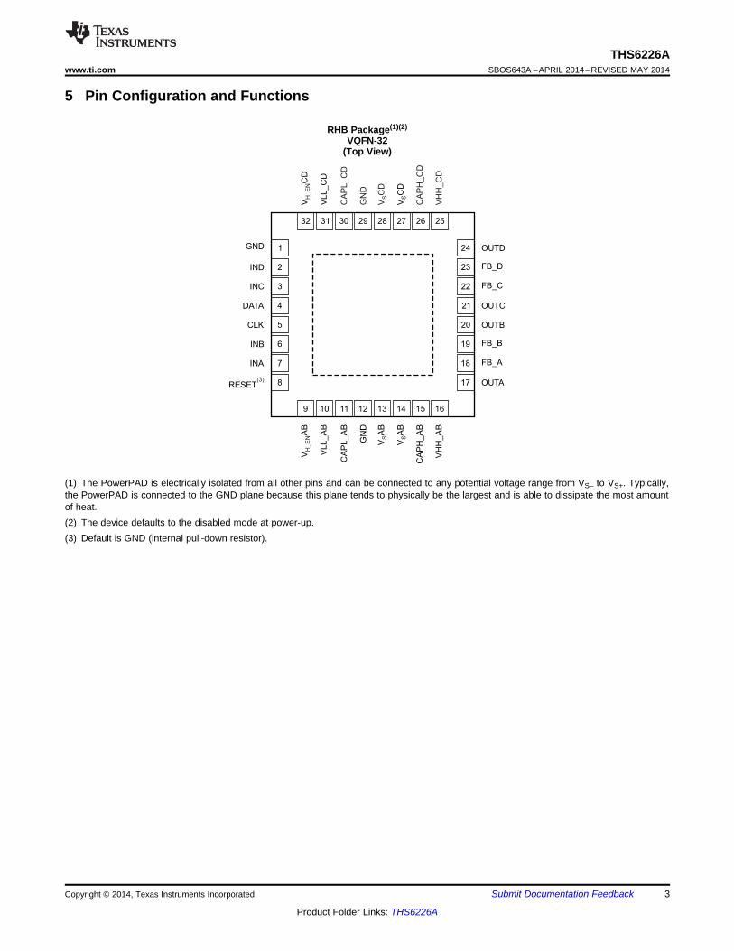
5 Pin Configuration and Functions
RHB Package(1)(2)
VQFN-32(Top View)
(1) The PowerPAD is electrically isolated from all other pins and can be connected to any potential voltage range from VS– to VS+. Typically,the PowerPAD is connected to the GND plane because this plane tends to physically be the largest and is able to dissipate the most amountof heat.(2) The device defaults to the disabled mode at power-up.(3) Default is GND (internal pull-down resistor).
Copyright © 2014, Texas Instruments Incorporated Submit Documentation Feedback 3
Product Folder Links: THS6226A
THS6226ASBOS643A –APRIL 2014–REVISED MAY 2014 www.ti.com
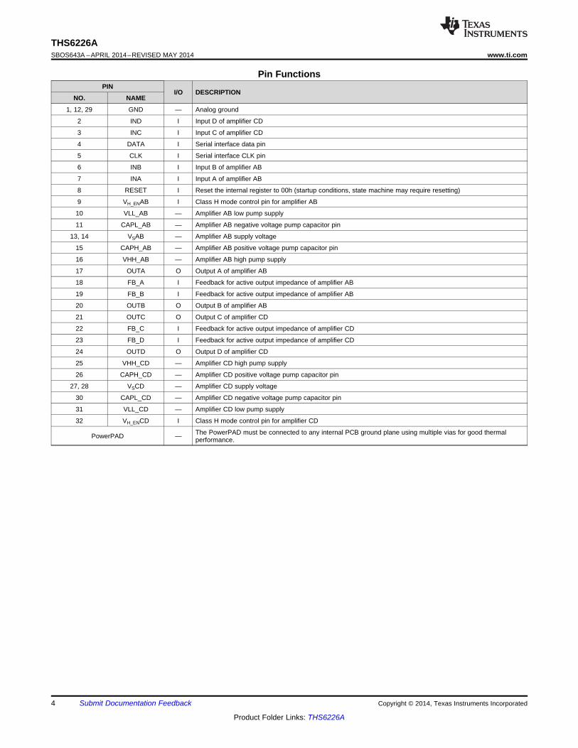
Pin FunctionsPIN
I/O DESCRIPTIONNO. NAME
1, 12, 29 GND — Analog ground
2 IND I Input D of amplifier CD
3 INC I Input C of amplifier CD
4 DATA I Serial interface data pin
5 CLK I Serial interface CLK pin
6 INB I Input B of amplifier AB
7 INA I Input A of amplifier AB
8 RESET I Reset the internal register to 00h (startup conditions, state machine may require resetting)
9 VH_ENAB I Class H mode control pin for amplifier AB
10 VLL_AB — Amplifier AB low pump supply
11 CAPL_AB — Amplifier AB negative voltage pump capacitor pin
13, 14 VSAB — Amplifier AB supply voltage
15 CAPH_AB — Amplifier AB positive voltage pump capacitor pin
16 VHH_AB — Amplifier AB high pump supply
17 OUTA O Output A of amplifier AB
18 FB_A I Feedback for active output impedance of amplifier AB
19 FB_B I Feedback for active output impedance of amplifier AB
20 OUTB O Output B of amplifier AB
21 OUTC O Output C of amplifier CD
22 FB_C I Feedback for active output impedance of amplifier CD
23 FB_D I Feedback for active output impedance of amplifier CD
24 OUTD O Output D of amplifier CD
25 VHH_CD — Amplifier CD high pump supply
26 CAPH_CD — Amplifier CD positive voltage pump capacitor pin
27, 28 VSCD — Amplifier CD supply voltage
30 CAPL_CD — Amplifier CD negative voltage pump capacitor pin
31 VLL_CD — Amplifier CD low pump supply
32 VH_ENCD I Class H mode control pin for amplifier CD
The PowerPAD must be connected to any internal PCB ground plane using multiple vias for good thermalPowerPAD — performance.
4 Submit Documentation Feedback Copyright © 2014, Texas Instruments Incorporated
Product Folder Links: THS6226A
THS6226Awww.ti.com SBOS643A –APRIL 2014–REVISED MAY 2014
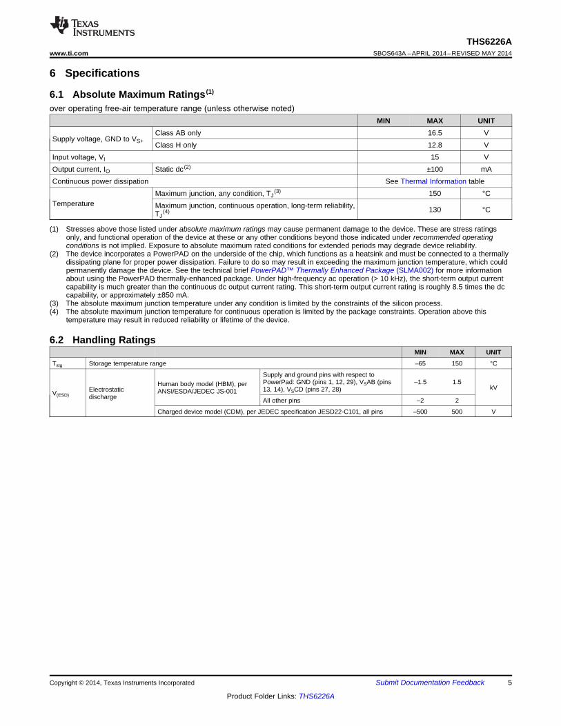
6 Specifications
6.1 Absolute Maximum Ratings (1)
over operating free-air temperature range (unless otherwise noted)MIN MAX UNIT
Class AB only 16.5 VSupply voltage, GND to VS+ Class H only 12.8 VInput voltage, VI 15 VOutput current, IO Static dc (2) ±100 mAContinuous power dissipation See Thermal Information table
Maximum junction, any condition, TJ(3) 150 °C
Temperature Maximum junction, continuous operation, long-term reliability, 130 °CTJ(4)
(1) Stresses above those listed under absolute maximum ratings may cause permanent damage to the device. These are stress ratingsonly, and functional operation of the device at these or any other conditions beyond those indicated under recommended operatingconditions is not implied. Exposure to absolute maximum rated conditions for extended periods may degrade device reliability.
(2) The device incorporates a PowerPAD on the underside of the chip, which functions as a heatsink and must be connected to a thermallydissipating plane for proper power dissipation. Failure to do so may result in exceeding the maximum junction temperature, which couldpermanently damage the device. See the technical brief PowerPAD™ Thermally Enhanced Package (SLMA002) for more informationabout using the PowerPAD thermally-enhanced package. Under high-frequency ac operation (> 10 kHz), the short-term output currentcapability is much greater than the continuous dc output current rating. This short-term output current rating is roughly 8.5 times the dccapability, or approximately ±850 mA.
(3) The absolute maximum junction temperature under any condition is limited by the constraints of the silicon process.(4) The absolute maximum junction temperature for continuous operation is limited by the package constraints. Operation above this
temperature may result in reduced reliability or lifetime of the device.
6.2 Handling RatingsMIN MAX UNIT
Tstg Storage temperature range –65 150 °C
Supply and ground pins with respect toPowerPad: GND (pins 1, 12, 29), VSAB (pins –1.5 1.5Human body model (HBM), per kV13, 14), VSCD (pins 27, 28)Electrostatic ANSI/ESDA/JEDEC JS-001V(ESD) discharge All other pins –2 2
Charged device model (CDM), per JEDEC specification JESD22-C101, all pins –500 500 V
Copyright © 2014, Texas Instruments Incorporated Submit Documentation Feedback 5
Product Folder Links: THS6226A

THS6226ASBOS643A –APRIL 2014–REVISED MAY 2014 www.ti.com
6.3 Recommended Operating Conditionsover operating free-air temperature range (unless otherwise noted)
MIN NOM MAX UNITClass H 10 12.6 V
Power-supply voltage rangeClass AB 10 15 V
Operating junction temperature –40 130 °C
6.4 Thermal InformationTHS6226A
THERMAL METRIC (1) RHB (VQFN) UNIT32 PINS
RθJA Junction-to-ambient thermal resistance 35.1RθJC(top) Junction-to-case (top) thermal resistance 22.1RθJB Junction-to-board thermal resistance 7.0
°C/WψJT Junction-to-top characterization parameter 0.3ψJB Junction-to-board characterization parameter 6.9RθJC(bot) Junction-to-case (bottom) thermal resistance 1.3
(1) For more information about traditional and new thermal metrics, see the IC Package Thermal Metrics application report, SPRA953.
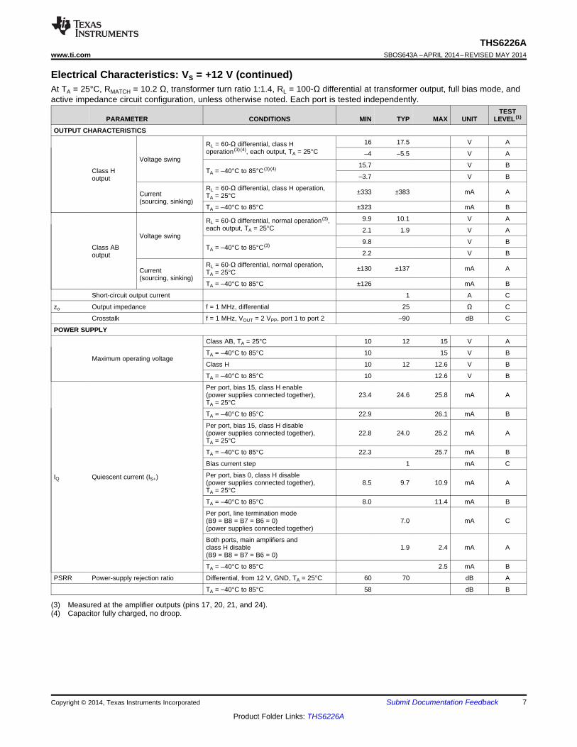
6.5 Electrical Characteristics: VS = +12 VAt TA = 25°C, RMATCH = 10.2 Ω, transformer turn ratio 1:1.4, RL = 100-Ω differential at transformer output, full bias mode, andactive impedance circuit configuration, unless otherwise noted. Each port is tested independently.
TESTPARAMETER CONDITIONS MIN TYP MAX UNIT LEVEL (1)
AC PERFORMANCE
VO = 2 VPP, differential atSmall-signal bandwidth, –3 dB 97 MHz COUTCD and OUTAB, gain = 19 V/V
0.1-dB bandwidth flatness VO = 2 VPP 30 MHz C
Large-signal bandwidth VO = 7.5 VPP 80 MHz C
SR Slew rate (10% to 90% level) VO = 15-V step, differential 1750 V/μs C
Rise-and-fall time VO = 2 VPP 3.6 ns C
Full bias, f = 1 MHz, VO = 2 VPP, –87 dBc CRL = 60-Ω differentialHD2 Second-harmonic distortion
Full bias, f = 5 MHz, VO = 2 VPP, –73 dBc CRL = 60-Ω differential
Full bias, f = 1 MHz, VO = 2 VPP, –83 dBc CRL = 60-Ω differentialHD3 Third-harmonic distortion
Full bias, f = 5 MHz, VO = 2 VPP, –71 dBc CRL = 60-Ω differential
Differential input voltage noise f = 1 MHz, input-referred 6.5 nV/√Hz C
DC PERFORMANCE
Differential gain Closed-loop configuration 19 V/V C
Differential gain error (2) TA = 25°C ±8% A
TA = 25°C ±1 ±10 mV AVIO Input offset voltage
TA = –40°C to 85°C ±11 mV B
Input offset voltage drift 15 μV/°C B
Channels 1 to 2 and 3 to 4 only,Input offset voltage matching ±1 ±10 mV ATA = 25°C
INPUT CHARACTERISTICS
Noninverting input resistance 2 || 2 kΩ || pF C
Input bias voltage TA = 25°C 5.8 6 6.2 V A
(1) Test levels: (A) 100% tested at 25°C. Overtemperature limits set by characterization and simulation. (B) Limits set by characterizationand simulation. (C) Typical value only for information.
(2) Negative feedback loop only.
6 Submit Documentation Feedback Copyright © 2014, Texas Instruments Incorporated
Product Folder Links: THS6226A
THS6226Awww.ti.com SBOS643A –APRIL 2014–REVISED MAY 2014
Electrical Characteristics: VS = +12 V (continued)At TA = 25°C, RMATCH = 10.2 Ω, transformer turn ratio 1:1.4, RL = 100-Ω differential at transformer output, full bias mode, andactive impedance circuit configuration, unless otherwise noted. Each port is tested independently.
TESTPARAMETER CONDITIONS MIN TYP MAX UNIT LEVEL (1)
OUTPUT CHARACTERISTICS
16 17.5 V ARL = 60-Ω differential, class Hoperation (3) (4), each output, TA = 25°C –4 –5.5 V A
Voltage swing15.7 V B
Class H TA = –40°C to 85°C (3) (4)
–3.7 V BoutputRL = 60-Ω differential, class H operation, ±333 ±383 mA ACurrent TA = 25°C
(sourcing, sinking)TA = –40°C to 85°C ±323 mA B
9.9 10.1 V ARL = 60-Ω differential, normal operation (3),each output, TA = 25°C 2.1 1.9 V A
Voltage swing9.8 V B
Class AB TA = –40°C to 85°C (3)
2.2 V BoutputRL = 60-Ω differential, normal operation, ±130 ±137 mA ACurrent TA = 25°C
(sourcing, sinking)TA = –40°C to 85°C ±126 mA B
Short-circuit output current 1 A C
zo Output impedance f = 1 MHz, differential 25 Ω C
Crosstalk f = 1 MHz, VOUT = 2 VPP, port 1 to port 2 –90 dB C
POWER SUPPLY
Class AB, TA = 25°C 10 12 15 V A
TA = –40°C to 85°C 10 15 V BMaximum operating voltage
Class H 10 12 12.6 V B
TA = –40°C to 85°C 10 12.6 V B
Per port, bias 15, class H enable(power supplies connected together), 23.4 24.6 25.8 mA ATA = 25°C
TA = –40°C to 85°C 22.9 26.1 mA B
Per port, bias 15, class H disable(power supplies connected together), 22.8 24.0 25.2 mA ATA = 25°C
TA = –40°C to 85°C 22.3 25.7 mA B
Bias current step 1 mA C
Per port, bias 0, class H disableIQ Quiescent current (IS+)(power supplies connected together), 8.5 9.7 10.9 mA ATA = 25°C
TA = –40°C to 85°C 8.0 11.4 mA B
Per port, line termination mode(B9 = B8 = B7 = B6 = 0) 7.0 mA C(power supplies connected together)
Both ports, main amplifiers andclass H disable 1.9 2.4 mA A(B9 = B8 = B7 = B6 = 0)
TA = –40°C to 85°C 2.5 mA B
PSRR Power-supply rejection ratio Differential, from 12 V, GND, TA = 25°C 60 70 dB A
TA = –40°C to 85°C 58 dB B
(3) Measured at the amplifier outputs (pins 17, 20, 21, and 24).(4) Capacitor fully charged, no droop.
Copyright © 2014, Texas Instruments Incorporated Submit Documentation Feedback 7
Product Folder Links: THS6226A
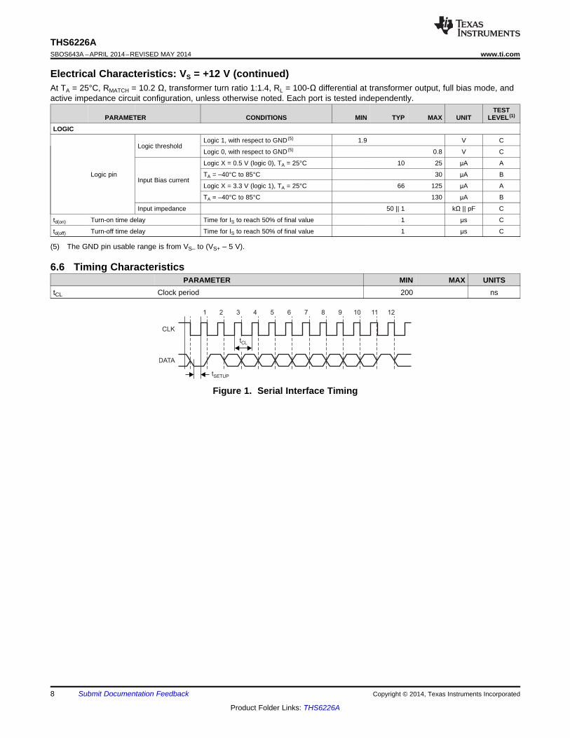
CLK
DATA
2 4 6 81 3 5 7 9 10 11 12
tSETUP
tCL
THS6226ASBOS643A –APRIL 2014–REVISED MAY 2014 www.ti.com
Electrical Characteristics: VS = +12 V (continued)At TA = 25°C, RMATCH = 10.2 Ω, transformer turn ratio 1:1.4, RL = 100-Ω differential at transformer output, full bias mode, andactive impedance circuit configuration, unless otherwise noted. Each port is tested independently.
TESTPARAMETER CONDITIONS MIN TYP MAX UNIT LEVEL (1)
LOGIC
Logic 1, with respect to GND (5) 1.9 V CLogic threshold
Logic 0, with respect to GND (5) 0.8 V C
Logic X = 0.5 V (logic 0), TA = 25°C 10 25 μA A
Logic pin TA = –40°C to 85°C 30 μA BInput Bias current
Logic X = 3.3 V (logic 1), TA = 25°C 66 125 μA A
TA = –40°C to 85°C 130 μA B
Input impedance 50 || 1 kΩ || pF C
td(on) Turn-on time delay Time for IS to reach 50% of final value 1 μs C
td(off) Turn-off time delay Time for IS to reach 50% of final value 1 μs C
(5) The GND pin usable range is from VS– to (VS+ – 5 V).
6.6 Timing CharacteristicsPARAMETER MIN MAX UNITS
tCL Clock period 200 ns
Figure 1. Serial Interface Timing
8 Submit Documentation Feedback Copyright © 2014, Texas Instruments Incorporated
Product Folder Links: THS6226A
0 2 4 6 8
10 12 14 16 18 20 22 24 26 28 30 32
0 5 10 15
Qui
esce
nt C
urre
nt (
mA
)
Supply Voltage (V)
Class H Bias 15
Class AB Bias 15
Class H Bias 0
Class AB Bias 0
C005
8
8.5
9
9.5
10
10.5
11
11.5
12
21
21.5
22
22.5
23
23.5
24
24.5
25
±50 ±25 0 25 50 75 100 125
Bia
s 0
Qui
esce
nt C
urre
nt (
mA
)
Bia
s 15
Qui
esce
nt C
urre
nt (
mA
)
Temperature (C)
Ch. AB Bias 15
Ch. CD Bias 15
Ch. AB Bias 15 Class H
Ch. CD Bias 15 Class H
Ch. AB Bias 0
Ch. CD Bias 0
C006
0
2
4
6
8
10
12
-350 -250 -150 -50 50 150 250 350
Out
put V
olta
ge (
V)
Output Current (mA) C003
25 : Load Line
1 W Internal Power Limit
1 W Internal Power Limit
50 : Load Line
100 : Load Line
±160 ±150 ±140 ±130 ±120 ±110 ±100 ±90 ±80 ±70 ±60 ±50 ±40 ±30
0 1 2 3 4 5 6 7 8 9 10 11 12 13 14 15 16 17 18
Pow
er D
ensi
ty (
dBm
/Hz)
Frequency (MHz)
Profile Adjacent Ch. Disabled
C004
-24
-21
-18
-15
-12
-9
-6
-3
0
3
1 10 100
Nor
mal
ized
Gai
n (d
B
Frequency (MHz)
Bias 0 Bias 1 Bias 2 Bias 3 Bias 4 Bias 5 Bias 6 Bias 7 Bias 8 Bias 9 Bias 10 Bias 11 Bias 12 Bias 13 Bias 14 Bias 15
C001
-24
-21
-18
-15
-12
-9
-6
-3
0
3
1 10 100
Nor
mal
ized
Gai
n (d
B
Frequency (MHz)
Bias 0 Bias 1 Bias 2 Bias 3 Bias 4 Bias 5 Bias 6 Bias 7 Bias 8 Bias 9 Bias 10 Bias 11 Bias 12 Bias 13 Bias 14 Bias 15
C002
THS6226Awww.ti.com SBOS643A –APRIL 2014–REVISED MAY 2014
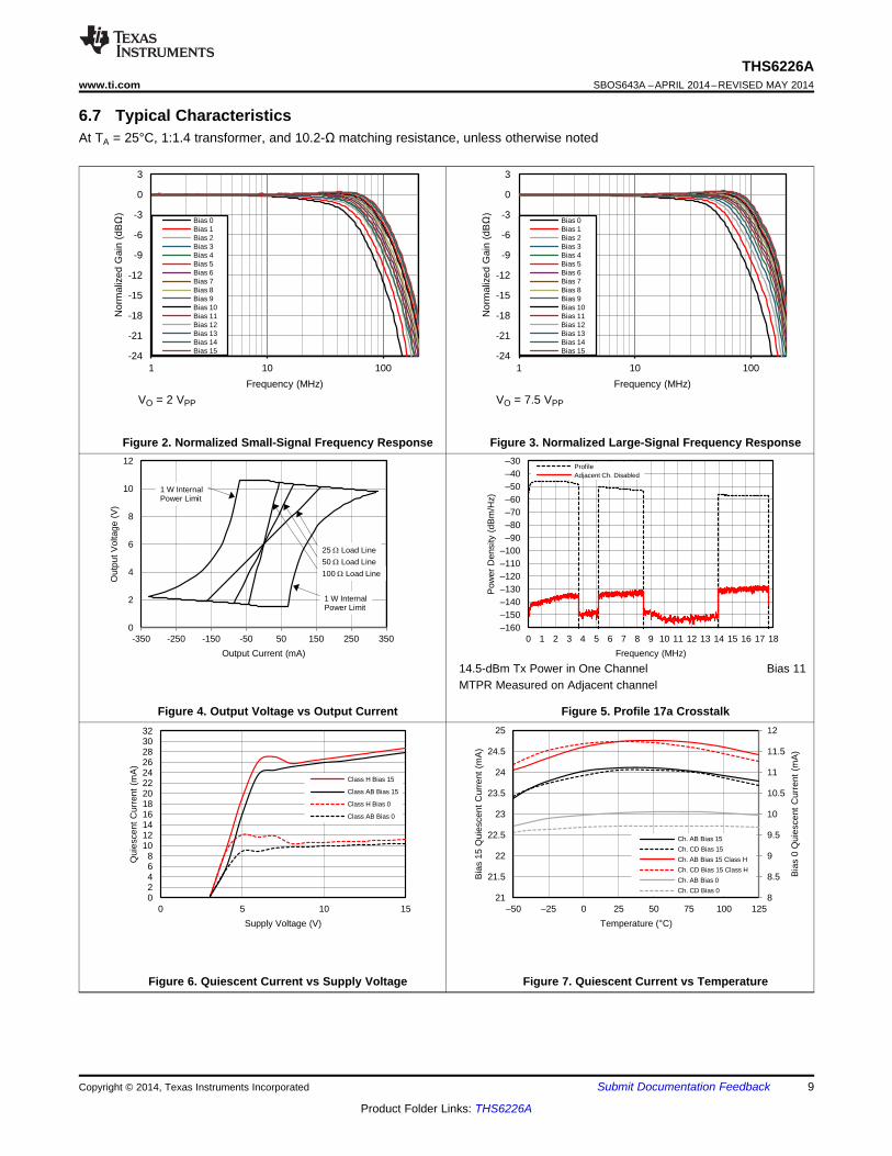
6.7 Typical CharacteristicsAt TA = 25°C, 1:1.4 transformer, and 10.2-Ω matching resistance, unless otherwise noted
VO = 2 VPP VO = 7.5 VPP
Figure 2. Normalized Small-Signal Frequency Response Figure 3. Normalized Large-Signal Frequency Response
14.5-dBm Tx Power in One Channel Bias 11MTPR Measured on Adjacent channel
Figure 4. Output Voltage vs Output Current Figure 5. Profile 17a Crosstalk
Figure 6. Quiescent Current vs Supply Voltage Figure 7. Quiescent Current vs Temperature
Copyright © 2014, Texas Instruments Incorporated Submit Documentation Feedback 9
Product Folder Links: THS6226A
200
250
300
350
400
450
500
±6 ±3 0 3 6 9 12 15
Pow
er C
onsu
mpt
ion
(mW
)
Tx Power (dBm)
Single Channel
Dual channel
C011
±130
±120
±110
±100
±90
±80
±70
±60
±50
±40
±30
0 1 2 3 4 5 6 7 8 9 10 11 12 13 14 15 16 17 18
Pow
er D
ensi
ty (
dBm
/Hz)
Frequency (MHz)
Profile Single Channel Dual Channel
C012
150
250
350
450
550
650
750
850
±6 ±3 0 3 6 9 12 15 18 21
Pow
er C
onsu
mpt
ion
(mW
)
Tx Power (dBm)
Single Channel
Dual channel
C009
±120
±110
±100
±90
±80
±70
±60
±50
±40
±30
0 1 2 3 4 5 6 7 8
Pow
er D
ensi
ty (
dBm
/Hz)
Frequency (MHz)
Profile Single Channel Dual Channel
C010
0
100
200
300
400
500
600
700
±10 ±5 0 5 10 15 20
Pow
er C
onsu
mpt
ion
(mW
)
Tx Power (dBm)
Single Channel Dual channel (per channel)
C007
±120
±110
±100
±90
±80
±70
±60
±50
±40
±30
0.25 0.5 0.75 1 1.25 1.5 1.75 2 2.25
Pow
er D
ensi
ty (
dBm
/Hz)
Frequency (MHz)
Profile
Single Channel
Dual Channel
C008
THS6226ASBOS643A –APRIL 2014–REVISED MAY 2014 www.ti.com
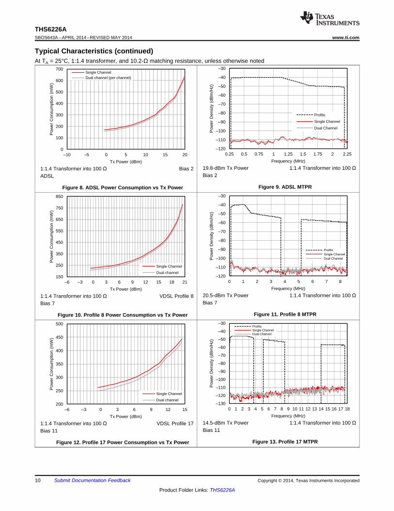
Typical Characteristics (continued)At TA = 25°C, 1:1.4 transformer, and 10.2-Ω matching resistance, unless otherwise noted
19.8-dBm Tx Power 1:1.4 Transformer into 100 Ω1:1.4 Transformer into 100 Ω Bias 2Bias 2ADSL
Figure 9. ADSL MTPRFigure 8. ADSL Power Consumption vs Tx Power
20.5-dBm Tx Power 1:1.4 Transformer into 100 Ω1:1.4 Transformer into 100 Ω VDSL Profile 8Bias 7Bias 7
Figure 11. Profile 8 MTPRFigure 10. Profile 8 Power Consumption vs Tx Power
14.5-dBm Tx Power 1:1.4 Transformer into 100 Ω1:1.4 Transformer into 100 Ω VDSL Profile 17Bias 11Bias 11
Figure 13. Profile 17 MTPRFigure 12. Profile 17 Power Consumption vs Tx Power
10 Submit Documentation Feedback Copyright © 2014, Texas Instruments Incorporated
Product Folder Links: THS6226A
250
300
350
400
450
500
±6 ±3 0 3 6 9 12 15
Pow
er C
onsu
mpt
ion
(mW
)
Tx Power (dBm)
Ta = +85C Ta = +25C Ta = -40C
C017
±130
±120
±110
±100
±90
±80
±70
±60
±50
±40
±30
0 1 2 3 4 5 6 7 8 9 10 11 12 13 14 15 16 17 18
Pow
er D
ensi
ty (
dBm
/Hz)
Frequency (MHz)
Profile Ta = +85C Ta = +25C Ta = -40C
C018
150
250
350
450
550
650
750
850
±6 ±3 0 3 6 9 12 15 18 21
Pow
er C
onsu
mpt
ion
(mW
)
Tx Power (dBm)
Ta = +85C Ta = +25C Ta = -40C
C015
±120
±110
±100
±90
±80
±70
±60
±50
±40
±30
0 1 2 3 4 5 6 7 8
Pow
er D
ensi
ty (
dBm
/Hz)
Frequency (MHz)
Profile Ta = +85C Ta = +25C Ta = -40C
C016
0
100
200
300
400
500
600
700
±10 ±5 0 5 10 15 20
Pow
er C
onsu
mpt
ion
(mW
)
Tx Power (dBm)
Ta = +85C Ta = +25C Ta = -40C
C013
±120
±110
±100
±90
±80
±70
±60
±50
±40
±30
0.25 0.5 0.75 1 1.25 1.5 1.75 2 2.25
Pow
er D
ensi
ty (
dBm
/Hz)
Frequency (MHz)
Profile Ta = +85C Ta = +25C Ta = -40C
C014
THS6226Awww.ti.com SBOS643A –APRIL 2014–REVISED MAY 2014
Typical Characteristics (continued)At TA = 25°C, 1:1.4 transformer, and 10.2-Ω matching resistance, unless otherwise noted
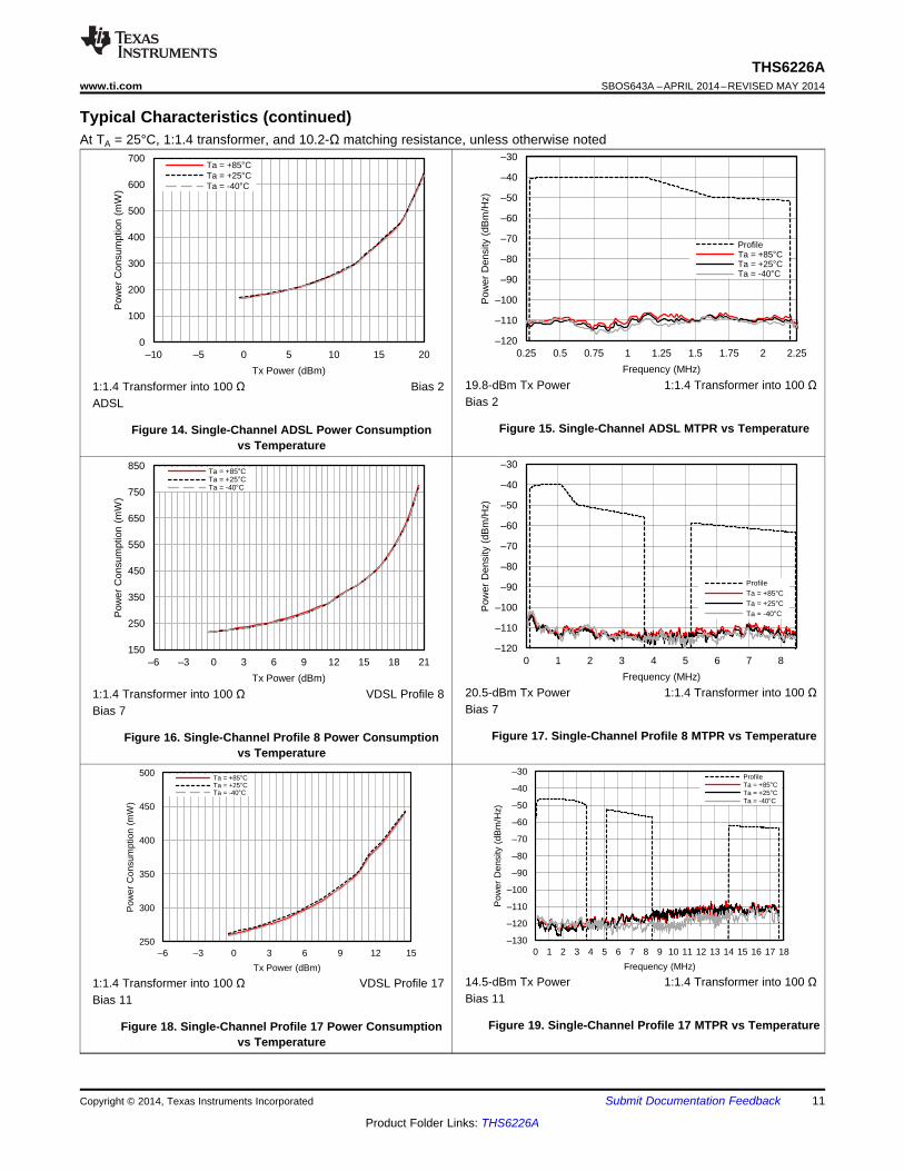
19.8-dBm Tx Power 1:1.4 Transformer into 100 Ω1:1.4 Transformer into 100 Ω Bias 2Bias 2ADSL
Figure 15. Single-Channel ADSL MTPR vs TemperatureFigure 14. Single-Channel ADSL Power Consumptionvs Temperature
20.5-dBm Tx Power 1:1.4 Transformer into 100 Ω1:1.4 Transformer into 100 Ω VDSL Profile 8Bias 7Bias 7
Figure 17. Single-Channel Profile 8 MTPR vs TemperatureFigure 16. Single-Channel Profile 8 Power Consumptionvs Temperature
14.5-dBm Tx Power 1:1.4 Transformer into 100 Ω1:1.4 Transformer into 100 Ω VDSL Profile 17Bias 11Bias 11
Figure 19. Single-Channel Profile 17 MTPR vs TemperatureFigure 18. Single-Channel Profile 17 Power Consumptionvs Temperature
Copyright © 2014, Texas Instruments Incorporated Submit Documentation Feedback 11
Product Folder Links: THS6226A
200
250
300
350
400
450
±6 ±3 0 3 6 9 12 15
Pow
er C
onsu
mpt
ion
(mW
)
Tx Power (dBm)
Ta = +85C Ta = +25C Ta = -40C
C023
±130
±120
±110
±100
±90
±80
±70
±60
±50
±40
±30
0 1 2 3 4 5 6 7 8 9 10 11 12 13 14 15 16 17 18
Pow
er D
ensi
ty (
dBm
/Hz)
Frequency (MHz)
Profile Ta = +85C Ta = +25C Ta = -40C
C024
150
250
350
450
550
650
750
850
±6 ±3 0 3 6 9 12 15 18 21
Pow
er C
onsu
mpt
ion
(mW
)
Tx Power (dBm)
Ta = +85C Ta = +25C Ta = -40C
C021
±120
±110
±100
±90
±80
±70
±60
±50
±40
±30
0 1 2 3 4 5 6 7 8
Pow
er D
ensi
ty (
dBm
/Hz)
Frequency (MHz)
Profile Ta = +85C Ta = +25C Ta = -40C
C022
0
100
200
300
400
500
600
700
±10 ±5 0 5 10 15 20
Pow
er C
onsu
mpt
ion
(mW
)
Tx Power (dBm)
Ta = +85C Ta = +25C Ta = -40C
C019
±120
±110
±100
±90
±80
±70
±60
±50
±40
±30
0.25 0.5 0.75 1 1.25 1.5 1.75 2 2.25
Pow
er D
ensi
ty (
dBm
/Hz)
Frequency (MHz)
Profile Ta = +85C Ta = +25C Ta = -40C
C020
THS6226ASBOS643A –APRIL 2014–REVISED MAY 2014 www.ti.com
Typical Characteristics (continued)At TA = 25°C, 1:1.4 transformer, and 10.2-Ω matching resistance, unless otherwise noted
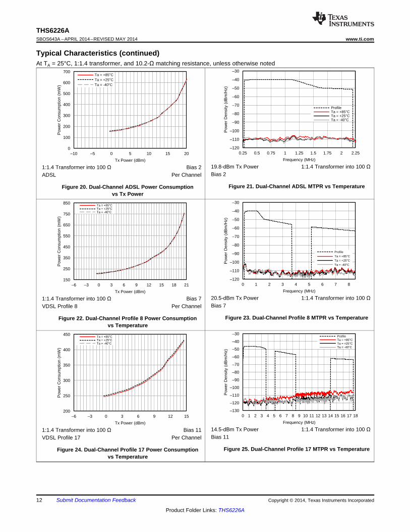
19.8-dBm Tx Power 1:1.4 Transformer into 100 Ω1:1.4 Transformer into 100 Ω Bias 2Bias 2ADSL Per Channel
Figure 21. Dual-Channel ADSL MTPR vs TemperatureFigure 20. Dual-Channel ADSL Power Consumptionvs Tx Power
20.5-dBm Tx Power 1:1.4 Transformer into 100 Ω1:1.4 Transformer into 100 Ω Bias 7Bias 7VDSL Profile 8 Per Channel
Figure 23. Dual-Channel Profile 8 MTPR vs TemperatureFigure 22. Dual-Channel Profile 8 Power Consumptionvs Temperature
14.5-dBm Tx Power 1:1.4 Transformer into 100 Ω1:1.4 Transformer into 100 Ω Bias 11Bias 11VDSL Profile 17 Per Channel
Figure 25. Dual-Channel Profile 17 MTPR vs TemperatureFigure 24. Dual-Channel Profile 17 Power Consumptionvs Temperature
12 Submit Documentation Feedback Copyright © 2014, Texas Instruments Incorporated
Product Folder Links: THS6226A
200
250
300
350
400
450
500
±6 ±3 0 3 6 9 12 15
Pow
er C
onsu
mpt
ion
(mW
)
Tx Power (dBm)
Ta = +85C Ta = +25C Ta = -40C
C029
±130
±120
±110
±100
±90
±80
±70
±60
±50
±40
±30
0 2 4 6 8 10 12 14 16 18 20 22 24 26 28 30 32
Pow
er D
ensi
ty (
dBm
/Hz)
Frequency (MHz)
Profile Ta = +85C Ta = +25C Ta = -40C
C030
200
250
300
350
400
450
500
±6 ±3 0 3 6 9 12 15
Pow
er C
onsu
mpt
ion
(mW
)
Tx Power (dBm)
Ta = +85C Ta = +25C Ta = -40C
C027
±130
±120
±110
±100
±90
±80
±70
±60
±50
±40
±30
0 2 4 6 8 10 12 14 16 18 20 22 24 26 28 30 32
Pow
er D
ensi
ty (
dBm
/Hz)
Frequency (MHz)
Profile Ta = +85C Ta = +25C Ta = -40C
C028
0
100
200
300
400
500
600
700
800
900
-10
-8.2
-6.2
-4.2
-2.2
-0.2
1.8
3.8
5.8
7.8
9.8
Cou
nt
Input Offset Voltage (mV) C026
-2
-1.5
-1
-0.5
0
0.5
1
1.5
2
±50 ±25 0 25 50 75 100 125
Inpu
t O
ffset
Vol
tage
(m
V)
Temperature (C)
Unit 1 Unit 2 Unit 3 Unit 4
C025
THS6226Awww.ti.com SBOS643A –APRIL 2014–REVISED MAY 2014
Typical Characteristics (continued)At TA = 25°C, 1:1.4 transformer, and 10.2-Ω matching resistance, unless otherwise noted
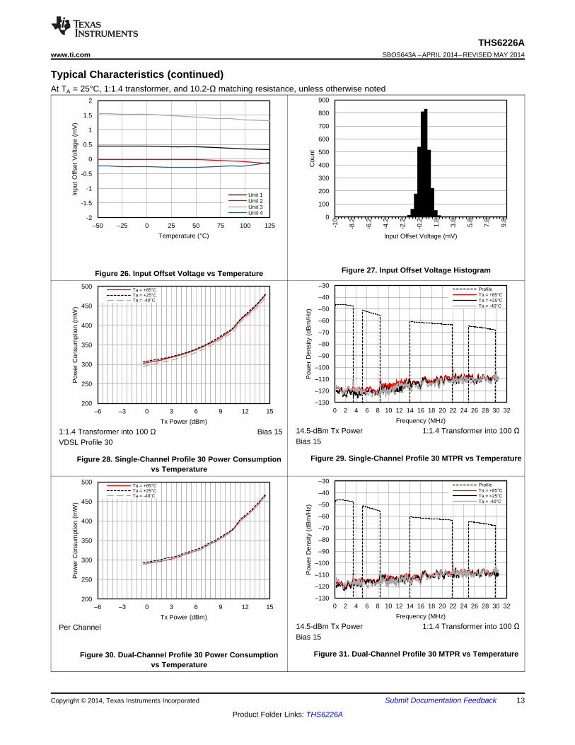
Figure 27. Input Offset Voltage HistogramFigure 26. Input Offset Voltage vs Temperature
14.5-dBm Tx Power 1:1.4 Transformer into 100 Ω1:1.4 Transformer into 100 Ω Bias 15Bias 15VDSL Profile 30
Figure 29. Single-Channel Profile 30 MTPR vs TemperatureFigure 28. Single-Channel Profile 30 Power Consumptionvs Temperature
14.5-dBm Tx Power 1:1.4 Transformer into 100 ΩPer ChannelBias 15
Figure 31. Dual-Channel Profile 30 MTPR vs TemperatureFigure 30. Dual-Channel Profile 30 Power Consumptionvs Temperature
Copyright © 2014, Texas Instruments Incorporated Submit Documentation Feedback 13
Product Folder Links: THS6226A
Class H Functions
Class H Functions
VLL_AB,VLL_CD
CAPL_AB,CAPL_CD
Bias
DATA CLK VHH_AB,VHH_CD
CAPH_AB,CAPH_CD
FB_B, FB_D
FB_A, FB_C
OUTA OUTC,
OUTB, DOUT
VoltageReference
IN_A, IN_C
IN_B, IN_D
RESET
THS6226ASBOS643A –APRIL 2014–REVISED MAY 2014 www.ti.com
7 Detailed Description
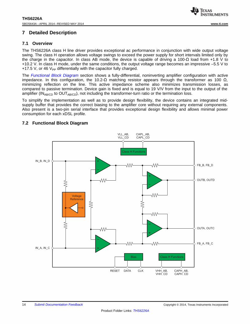
7.1 OverviewThe THS6226A class H line driver provides exceptional ac performance in conjunction with wide output voltageswing. The class H operation allows voltage swings to exceed the power supply for short intervals limited only bythe charge in the capacitor. In class AB mode, the device is capable of driving a 100-Ω load from +1.8 V to+10.2 V. In class H mode, under the same conditions, the output voltage range becomes an impressive –5.5 V to+17.5 V, or 46 VPP differentially with the capacitor fully charged.
The Functional Block Diagram section shows a fully-differential, noninverting amplifier configuration with activeimpedance. In this configuration, the 10.2-Ω matching resistor appears through the transformer as 100 Ω,minimizing reflection on the line. This active impedance scheme also minimizes transmission losses, ascompared to passive termination. Device gain is fixed and is equal to 19 V/V from the input to the output of theamplifier (INAB/CD to OUTAB/CD), not including the transformer-turn ratio or the termination loss.
To simplify the implementation as well as to provide design flexibility, the device contains an integrated mid-supply buffer that provides the correct biasing to the amplifier core without requiring any external components.Also present is a two-pin serial interface that provides exceptional design flexibility and allows minimal powerconsumption for each xDSL profile.
7.2 Functional Block Diagram
14 Submit Documentation Feedback Copyright © 2014, Texas Instruments Incorporated
Product Folder Links: THS6226A
THS6226Awww.ti.com SBOS643A –APRIL 2014–REVISED MAY 2014
7.3 Feature DescriptionThe device incorporates several hardware and functionality features: a high output current line driver, a chargepump, a voltage reference, a logic circuit, an active impedance, and a RESET pin. The device has two ports.Each port consists of a high output current line driver, a charge pump, and a reference voltage. Common circuitsare the RESET feature and the logic circuit.
7.3.1 High Output Current Line DriverThe main purpose for the device is to provide a high output current into a heavy load. For the THS6226A, with itsxDSL application targeted, the load is typically 100 Ω and currents as high as 400 mA are supported withexcellent linearity. The core of the line driver is a class AB amplifier providing both good efficiency and highcurrent drive capability. The high output line driver is the core of the device and any external circuit interface islocated on both the device inputs and output.
7.3.2 Charge PumpThe class H functionality of the device is brought on by the integration of a charge pump. The charge pump is apower-supply function to the line driver. The role of the charge pump is to vary the power supply from (12 V /GND) to (20 V / –8 V) and allow the line driver to support high peak to average ratio (PAR) signals whileminimizing power consumption and maintaining excellent linearity. The charge pump is controlled externally bythe VH_EN pin. A logic high on the VH_EN pin results in the power supply of the class AB line driver going to (20 V /–8 V), while a logic low on the VH_EN pin results in normal operation under the (12 V / GND) supplies.
7.3.3 Voltage ReferenceAn internal voltage reference provides the device common-mode input and output voltage.
7.3.4 LogicThe DATA and CLK pins allow access to the internal logic circuit implemented in the device. This logic circuitallows each channel to either be programmed individually for quiescent current, turn the charge pump on or off,disable the main amplifier, or select the line termination mode. For more information on programming, refer to theProgramming section.
7.3.5 Active ImpedanceThe line driver incorporates the positive feedback path to provide the termination to the load. For the device, thesynthesis factor implemented is 5.
7.3.6 RESET PinThe RESET pin provides a quick and easy way to disable the two ports immediately if a fault condition on theline occurs.
7.4 Device Functional ModesThere are several functional modes for the device. These functional modes can be accessed with the CLK andDATA pins. Each main line driver quiescent current can be set to 16 different bias modes: bias 0 through bias15. Additionally, the line driver and class H feature can be controlled to have the following configuration:
• Class AB mode is the main line driver by itself. The output voltage is limited by the (12 V / GND) power-supply rails. The quiescent current is then set by four bits.
• Class H mode is the main line driver used in conjunction with the class H feature. The output voltage islimited by the (20 V / –8 V) internally-generated power-supply rails. The quiescent current of the main linedriver is set by four bits, as in class AB mode.
• Line termination mode is the powered-down mode for the line driver. This mode maintains line termination buthas reduced linearity performance.
• Disabled mode.
For more information on these mode, refer to the Programming section.
Copyright © 2014, Texas Instruments Incorporated Submit Documentation Feedback 15
Product Folder Links: THS6226A

DATA B0 B1 B2 B3 B4 B5 B6 B7 B8 B9 B10 B11
Start
Bit
Start
Bit
Ch AB
Select
Ch CD
Select
PD1 PD0 D3 D2 D1 D0 Parity Stop
Bit
MSB LSB
THS6226ASBOS643A –APRIL 2014–REVISED MAY 2014 www.ti.com
7.5 Programming
7.5.1 Programming the DeviceProgramming the device is accomplished through a serial interface (pins 4 and 5) and proceeds in the followingsequence:• Two start bits are required (B0 = 0 followed by B1 = 1).• B2 through B9 are used to program the device. (Table 1 lists the bit descriptions.)• B10 (described in Table 2) is the parity bit that controls whether the word is loaded or not.• B11 is the stop bit and must be set to B11 = 1.
Figure 32 shows the required sequence.
Table 1. DATA SequencePARAMETER DESCRIPTION
B0, B1 Start bitsB2, B3 Channel selectB4, B5 Power-down featuresB6-B9 Quiescent current settingB10 Parity bitB11 Stop bit
Table 2. Parity BitB10 ODD PARITY BIT
0 For an odd number of high bits in B2 to B9, set B10 to 01 For an even number of high bits in B2 to B9, set B10 to 1
Figure 32. DATA Description
16 Submit Documentation Feedback Copyright © 2014, Texas Instruments Incorporated
Product Folder Links: THS6226A
THS6226Awww.ti.com SBOS643A –APRIL 2014–REVISED MAY 2014
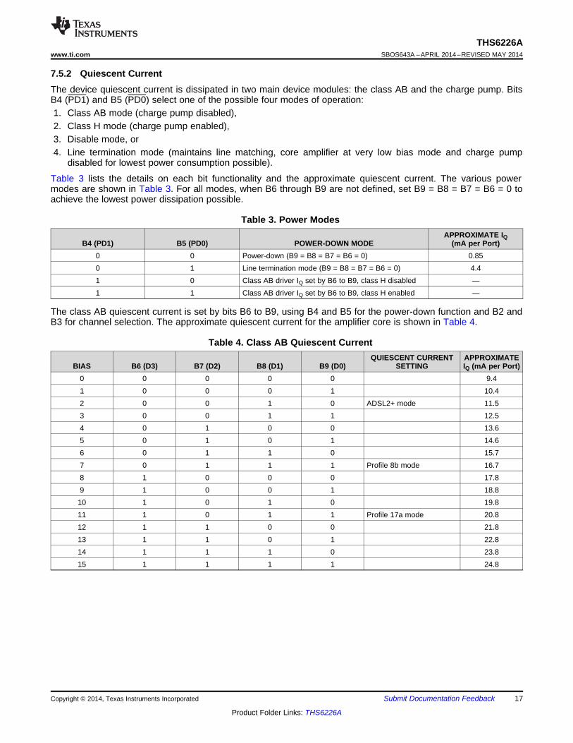
7.5.2 Quiescent CurrentThe device quiescent current is dissipated in two main device modules: the class AB and the charge pump. BitsB4 (PD1) and B5 (PD0) select one of the possible four modes of operation:1. Class AB mode (charge pump disabled),2. Class H mode (charge pump enabled),3. Disable mode, or4. Line termination mode (maintains line matching, core amplifier at very low bias mode and charge pump
disabled for lowest power consumption possible).
Table 3 lists the details on each bit functionality and the approximate quiescent current. The various powermodes are shown in Table 3. For all modes, when B6 through B9 are not defined, set B9 = B8 = B7 = B6 = 0 toachieve the lowest power dissipation possible.
Table 3. Power ModesAPPROXIMATE IQ
B4 (PD1) B5 (PD0) POWER-DOWN MODE (mA per Port)0 0 Power-down (B9 = B8 = B7 = B6 = 0) 0.850 1 Line termination mode (B9 = B8 = B7 = B6 = 0) 4.41 0 Class AB driver IQ set by B6 to B9, class H disabled —1 1 Class AB driver IQ set by B6 to B9, class H enabled —
The class AB quiescent current is set by bits B6 to B9, using B4 and B5 for the power-down function and B2 andB3 for channel selection. The approximate quiescent current for the amplifier core is shown in Table 4.
Table 4. Class AB Quiescent CurrentQUIESCENT CURRENT APPROXIMATE
BIAS B6 (D3) B7 (D2) B8 (D1) B9 (D0) SETTING IQ (mA per Port)0 0 0 0 0 9.41 0 0 0 1 10.42 0 0 1 0 ADSL2+ mode 11.53 0 0 1 1 12.54 0 1 0 0 13.65 0 1 0 1 14.66 0 1 1 0 15.77 0 1 1 1 Profile 8b mode 16.78 1 0 0 0 17.89 1 0 0 1 18.8
10 1 0 1 0 19.811 1 0 1 1 Profile 17a mode 20.812 1 1 0 0 21.813 1 1 0 1 22.814 1 1 1 0 23.815 1 1 1 1 24.8
Copyright © 2014, Texas Instruments Incorporated Submit Documentation Feedback 17
Product Folder Links: THS6226A
THS6226ASBOS643A –APRIL 2014–REVISED MAY 2014 www.ti.com
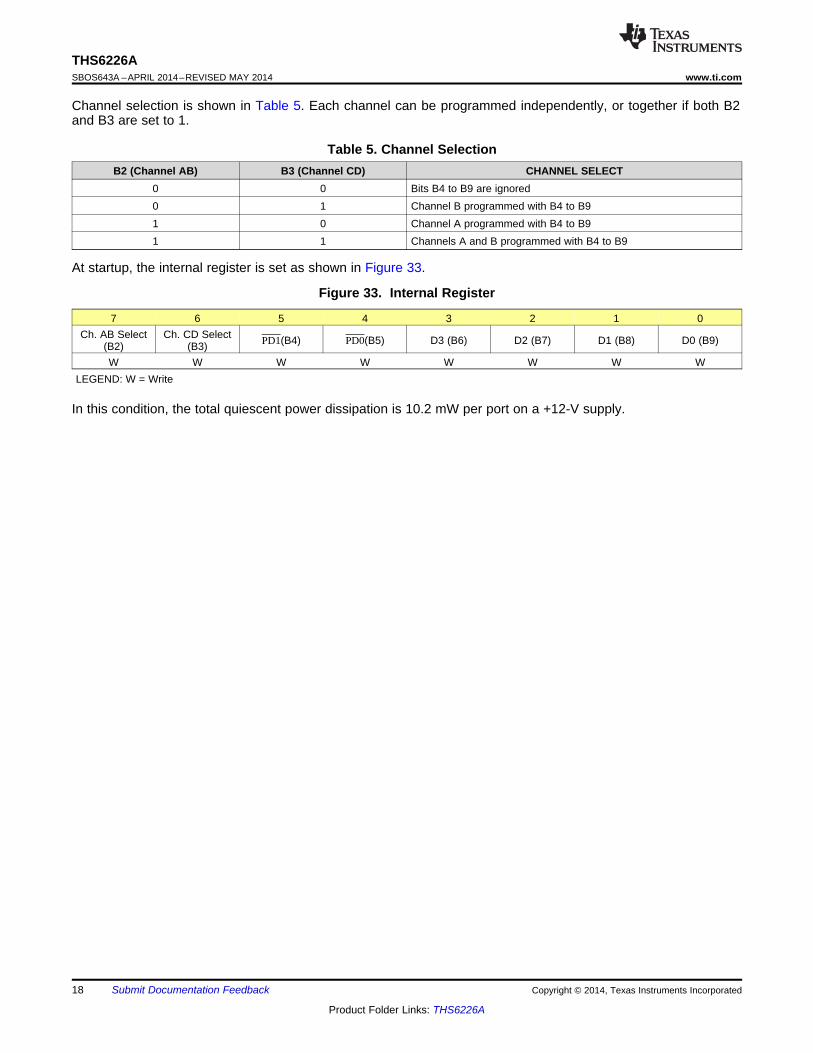
Channel selection is shown in Table 5. Each channel can be programmed independently, or together if both B2and B3 are set to 1.
Table 5. Channel SelectionB2 (Channel AB) B3 (Channel CD) CHANNEL SELECT
0 0 Bits B4 to B9 are ignored0 1 Channel B programmed with B4 to B91 0 Channel A programmed with B4 to B91 1 Channels A and B programmed with B4 to B9
At startup, the internal register is set as shown in Figure 33.
Figure 33. Internal Register
7 6 5 4 3 2 1 0Ch. AB Select Ch. CD Select PD1(B4) PD0(B5) D3 (B6) D2 (B7) D1 (B8) D0 (B9)(B2) (B3)
W W W W W W W WLEGEND: W = Write
In this condition, the total quiescent power dissipation is 10.2 mW per port on a +12-V supply.
18 Submit Documentation Feedback Copyright © 2014, Texas Instruments Incorporated
Product Folder Links: THS6226A
VIN+
VIN-
+12V
33 nF
Device1:n
100kW
+12V
CLK
DATA
1 Fm
1 Fm
OUTD
OUTC
IND
INC
VLL_CD
VHH_CD
CAPL_CD
CAPH_CD
FBC
FBD
RL0.2 ×
n2
RL
47 W
47 W
Se
co
nd
ary
Pro
tectio
n
THS6226Awww.ti.com SBOS643A –APRIL 2014–REVISED MAY 2014
8 Applications and Implementation
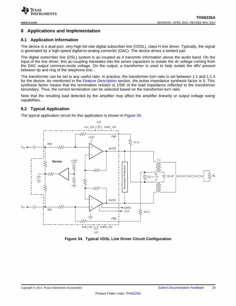
8.1 Application InformationThe device is a dual-port, very-high-bit-rate digital subscriber line (VDSL), class H line driver. Typically, the signalis generated by a high-speed digital-to-analog converter (DAC). The device drives a twisted pair.
The digital subscriber line (DSL) system is ac-coupled as it transmits information above the audio band. On theinput of the line driver, this ac-coupling translates into the series capacitors to isolate the dc voltage coming fromthe DAC output common-mode voltage. On the output, a transformer is used to help isolate the 48V presentbetween tip and ring of the telephone line.
The transformer can be set to any useful ratio. In practice, the transformer-turn ratio is set between 1:1 and 1:1.4for the device. As mentioned in the Feature Description section, the active impedance synthesis factor is 5. Thissynthesis factor means that the termination resistor is 1/5th of the load impedance reflected to the transformersecondary. Thus, the correct termination can be selected based on the transformer-turn ratio.
Note that the resulting load detected by the amplifier may affect the amplifier linearity or output voltage swingcapabilities.
8.2 Typical ApplicationThe typical application circuit for this application is shown in Figure 34.
Figure 34. Typical VDSL Line Driver Circuit Configuration
Copyright © 2014, Texas Instruments Incorporated Submit Documentation Feedback 19
Product Folder Links: THS6226A
THS6226ASBOS643A –APRIL 2014–REVISED MAY 2014 www.ti.com
Typical Application (continued)8.2.1 Design Requirements
Table 6. Design RequirementsDESIGN REQUIREMENT CONDITION
AC-coupling capacitors 0.1 µFSynthesis factor 5
Output transformer ratio 1:1.4Surge protection circuit Not shown
8.2.2 Detailed Design ProcedureThe input capacitor forms a high-pass filter with the device input impedance. This pole must be set at afrequency low enough to not interfere with the desired signal.
The output transformer can be changed to any transformer-turn ratio. Note that the load is expected to be atransmission line with 100-Ω characteristic impedance. Referred to the transformer secondary, the load detectedby the amplifier is 1 / n2 with 1:n being the transformer-turn ratio.
Practical limitations force the transformer-turn ratio to be between 1.4:1 and 1:2. At the lighter load detected bythe amplifier (1.4:1), the voltage swing is limited by the class H and the maximum achievable swing of theamplifier. At the heaviest load (1:2), the voltage swing is limited by the current drive capability of the amplifier. Tosatisfy the synthesis impedance factor and the loading, the series resistance (RS) can be set to RS = RL / 5 =100 Ω / (5 × n2).
For the charge pump, consider the thermal characteristic of the capacitor (X7R, X5R, or Y5V can be used for thecharge pump).
For the power-supply bypass, consider using only X7R or X5R because of the better stability of these materialsover temperature.
For surge protection, consider adding 47-Ω resistors in series on the positive feedback path. The secondaryprotection is also normally added after the series resistance on the secondary transformer.
20 Submit Documentation Feedback Copyright © 2014, Texas Instruments Incorporated
Product Folder Links: THS6226A
±130
±120
±110
±100
±90
±80
±70
±60
±50
±40
±30
0 1 2 3 4 5 6 7 8 9 10 11 12 13 14 15 16 17 18
Pow
er D
ensi
ty (
dBm
/Hz)
Frequency (MHz)
Profile Single Channel Dual Channel
C012
±120
±110
±100
±90
±80
±70
±60
±50
±40
±30
0.25 0.5 0.75 1 1.25 1.5 1.75 2 2.25
Pow
er D
ensi
ty (
dBm
/Hz)
Frequency (MHz)
Profile
Single Channel
Dual Channel
C008
±120
±110
±100
±90
±80
±70
±60
±50
±40
±30
0 1 2 3 4 5 6 7 8
Pow
er D
ensi
ty (
dBm
/Hz)
Frequency (MHz)
Profile Single Channel Dual Channel
C010
THS6226Awww.ti.com SBOS643A –APRIL 2014–REVISED MAY 2014
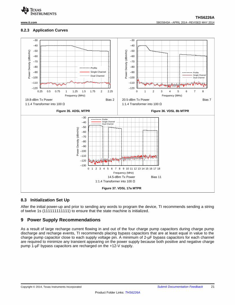
8.2.3 Application Curves
19.8-dBm Tx Power Bias 2 20.5-dBm Tx Power Bias 71:1.4 Transformer into 100 Ω 1:1.4 Transformer into 100 Ω
Figure 35. ADSL MTPR Figure 36. VDSL 8b MTPR
14.5-dBm Tx Power Bias 111:1.4 Transformer into 100 Ω
Figure 37. VDSL 17a MTPR
8.3 Initialization Set UpAfter the initial power-up and prior to sending any words to program the device, TI recommends sending a stringof twelve 1s (111111111111) to ensure that the state machine is initialized.
9 Power Supply Recommendations
As a result of large recharge current flowing in and out of the four charge pump capacitors during charge pumpdischarge and recharge events, TI recommends placing bypass capacitors that are at least equal in value to thecharge pump capacitor close to each supply voltage pin. A minimum of 2-µF bypass capacitors for each channelare required to minimize any transient appearing on the power supply because both positive and negative chargepump 1-µF bypass capacitors are recharged on the +12-V supply.
Copyright © 2014, Texas Instruments Incorporated Submit Documentation Feedback 21
Product Folder Links: THS6226A
THS6226ASBOS643A –APRIL 2014–REVISED MAY 2014 www.ti.com
10 Layout
10.1 Layout GuidelinesAchieving optimum performance with a high-frequency amplifier such as the THS6226A requires careful attentionto board layout parasitics and external component types. Recommendations that optimize performance include:a. Minimize parasitic capacitance to any ac ground for all signal I/O pins. Excessive parasitic capacitance on
the inverting input pin can cause instability. In the line driver application, the parasitic capacitance forms apole with the load detected by the amplifier and may reduce the effective bandwidth of the application circuit,thus leading to degraded performance. To reduce unwanted capacitance, open a window around the signalI/O pins in all ground and power planes around those pins. Otherwise, make sure that ground and powerplanes are unbroken elsewhere on the board.
b. Minimize the distance (< 0.25") from the power-supply pins to high-frequency 0.1-µF decoupling capacitors.At the device pins, make sure that the ground and power-plane layout are not in close proximity to the signalI/O pins. Avoid narrow power and ground traces to minimize inductance between the pins and decouplingcapacitors. Always decouple the power-supply connections with these capacitors. An additional low ESRsupply decoupling capacitor (≥ 2 µF, X7R or X5R) to ground is necessary to provide a transient currentduring the charge pump capacitors recharge.
c. Careful selection and placement of external components preserves the high-frequency performanceof the device. Use very low reactance type resistors. Surface-mount resistors function best and allow atighter overall layout. Metal-film or carbon composition, axially-leaded resistors also provide good high-frequency performance. Again, keep the leads and printed circuit board traces as short as possible. Neveruse wire-wound type resistors in a high-frequency application.
d. Connections to other wideband devices on the board can be made with short, direct traces or throughonboard transmission lines. For short connections, consider the trace and the input to the next device as alumped capacitive load. Use relatively wide traces (50 mils to 100 mils), preferably with ground and powerplanes opened up around them.
e. Do not socket a high-speed part such as the THS6226A. The additional lead length and pin-to-pincapacitance introduced by the socket can create an extremely troublesome parasitic network that makesachieving a smooth, stable frequency response almost impossible. Best results are obtained by soldering thedevice onto the board.
22 Submit Documentation Feedback Copyright © 2014, Texas Instruments Incorporated
Product Folder Links: THS6226A
Byp
ass
Cap
acit
orCharge Pump
CapacitorCharge Pump
Capacitor
Charge PumpPlaced to Minimize
Parasitic Series Resistance
Charge PumpCapacitor
Charge PumpCapacitor
Byp
ass
Cap
acit
or
GND
GN
DG
ND
+V
S+
SV
CA
PH
_A
BC
AP
H_C
D
VH
H_C
DV
HH
_A
B
CA
PL
_C
DC
AP
L_A
B
VL
L_C
DV
LL
_A
B
VH
_C
DE
NV
EN
H_A
B
THS6226Awww.ti.com SBOS643A –APRIL 2014–REVISED MAY 2014
10.2 Layout Example
Figure 38. Layout Example
Copyright © 2014, Texas Instruments Incorporated Submit Documentation Feedback 23
Product Folder Links: THS6226A
THS6226ASBOS643A –APRIL 2014–REVISED MAY 2014 www.ti.com
11 Device and Documentation Support
11.1 Documentation Support
11.1.1 Related DocumentationFor related documentation see the following:• PowerPAD™ Thermally Enhanced Package, SLMA002
11.2 TrademarksPowerPAD is a trademark of Texas Instruments, Inc.All other trademarks are the property of their respective owners.
11.3 Electrostatic Discharge CautionThese devices have limited built-in ESD protection. The leads should be shorted together or the device placed in conductive foamduring storage or handling to prevent electrostatic damage to the MOS gates.
11.4 GlossarySLYZ022 — TI Glossary.
This glossary lists and explains terms, acronyms and definitions.
12 Mechanical, Packaging, and Orderable InformationThe following pages include mechanical packaging and orderable information. This information is the mostcurrent data available for the designated devices. This data is subject to change without notice and revision ofthis document. For browser-based versions of this data sheet, refer to the left-hand navigation.
24 Submit Documentation Feedback Copyright © 2014, Texas Instruments Incorporated
Product Folder Links: THS6226A
PACKAGE OPTION ADDENDUM
www.ti.com 29-May-2014
Addendum-Page 1
PACKAGING INFORMATION
Orderable Device Status(1)
Package Type PackageDrawing
Pins PackageQty
Eco Plan(2)
Lead/Ball Finish(6)
MSL Peak Temp(3)
Op Temp (°C) Device Marking(4/5)
Samples
THS6226AIRHBR ACTIVE VQFN RHB 32 3000 Green (RoHS& no Sb/Br)
CU NIPDAU Level-3-260C-168 HR -40 to 85 HS6226AIRHB
THS6226AIRHBT ACTIVE VQFN RHB 32 250 Green (RoHS& no Sb/Br)
CU NIPDAU Level-3-260C-168 HR -40 to 85 HS6226AIRHB
(1) The marketing status values are defined as follows:ACTIVE: Product device recommended for new designs.LIFEBUY: TI has announced that the device will be discontinued, and a lifetime-buy period is in effect.NRND: Not recommended for new designs. Device is in production to support existing customers, but TI does not recommend using this part in a new design.PREVIEW: Device has been announced but is not in production. Samples may or may not be available.OBSOLETE: TI has discontinued the production of the device.
(2) Eco Plan - The planned eco-friendly classification: Pb-Free (RoHS), Pb-Free (RoHS Exempt), or Green (RoHS & no Sb/Br) - please check http://www.ti.com/productcontent for the latest availabilityinformation and additional product content details.TBD: The Pb-Free/Green conversion plan has not been defined.Pb-Free (RoHS): TI's terms "Lead-Free" or "Pb-Free" mean semiconductor products that are compatible with the current RoHS requirements for all 6 substances, including the requirement thatlead not exceed 0.1% by weight in homogeneous materials. Where designed to be soldered at high temperatures, TI Pb-Free products are suitable for use in specified lead-free processes.Pb-Free (RoHS Exempt): This component has a RoHS exemption for either 1) lead-based flip-chip solder bumps used between the die and package, or 2) lead-based die adhesive used betweenthe die and leadframe. The component is otherwise considered Pb-Free (RoHS compatible) as defined above.Green (RoHS & no Sb/Br): TI defines "Green" to mean Pb-Free (RoHS compatible), and free of Bromine (Br) and Antimony (Sb) based flame retardants (Br or Sb do not exceed 0.1% by weightin homogeneous material)
(3) MSL, Peak Temp. - The Moisture Sensitivity Level rating according to the JEDEC industry standard classifications, and peak solder temperature.
(4) There may be additional marking, which relates to the logo, the lot trace code information, or the environmental category on the device.
(5) Multiple Device Markings will be inside parentheses. Only one Device Marking contained in parentheses and separated by a "~" will appear on a device. If a line is indented then it is a continuationof the previous line and the two combined represent the entire Device Marking for that device.
(6) Lead/Ball Finish - Orderable Devices may have multiple material finish options. Finish options are separated by a vertical ruled line. Lead/Ball Finish values may wrap to two lines if the finishvalue exceeds the maximum column width.
Important Information and Disclaimer:The information provided on this page represents TI's knowledge and belief as of the date that it is provided. TI bases its knowledge and belief on informationprovided by third parties, and makes no representation or warranty as to the accuracy of such information. Efforts are underway to better integrate information from third parties. TI has taken andcontinues to take reasonable steps to provide representative and accurate information but may not have conducted destructive testing or chemical analysis on incoming materials and chemicals.TI and TI suppliers consider certain information to be proprietary, and thus CAS numbers and other limited information may not be available for release.
PACKAGE OPTION ADDENDUM
www.ti.com 29-May-2014
Addendum-Page 2
In no event shall TI's liability arising out of such information exceed the total purchase price of the TI part(s) at issue in this document sold by TI to Customer on an annual basis.
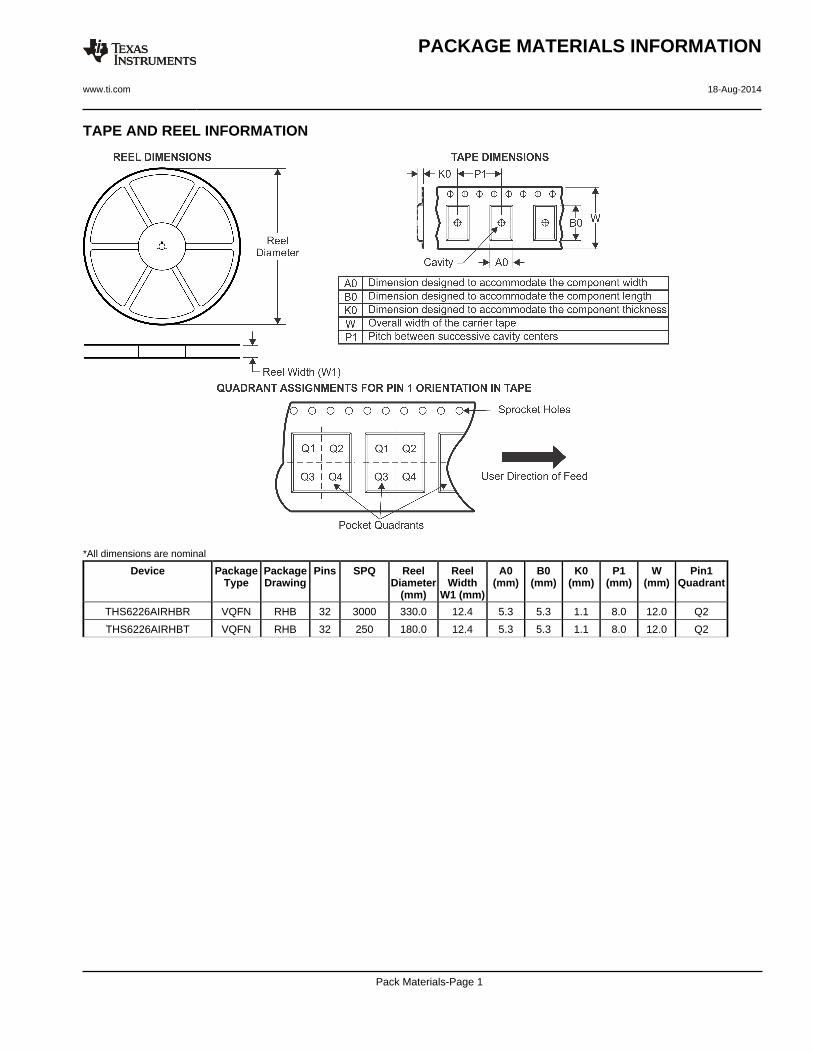
TAPE AND REEL INFORMATION
*All dimensions are nominal
Device PackageType
PackageDrawing
Pins SPQ ReelDiameter
(mm)
ReelWidth
W1 (mm)
A0(mm)
B0(mm)
K0(mm)
P1(mm)
W(mm)
Pin1Quadrant
THS6226AIRHBR VQFN RHB 32 3000 330.0 12.4 5.3 5.3 1.1 8.0 12.0 Q2
THS6226AIRHBT VQFN RHB 32 250 180.0 12.4 5.3 5.3 1.1 8.0 12.0 Q2
PACKAGE MATERIALS INFORMATION
www.ti.com 18-Aug-2014
Pack Materials-Page 1
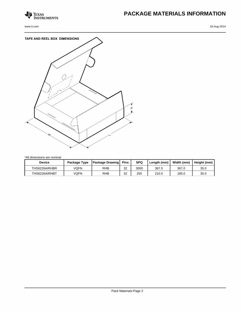
*All dimensions are nominal
Device Package Type Package Drawing Pins SPQ Length (mm) Width (mm) Height (mm)
THS6226AIRHBR VQFN RHB 32 3000 367.0 367.0 35.0
THS6226AIRHBT VQFN RHB 32 250 210.0 185.0 35.0
PACKAGE MATERIALS INFORMATION
www.ti.com 18-Aug-2014
Pack Materials-Page 2

IMPORTANT NOTICE
Texas Instruments Incorporated and its subsidiaries (TI) reserve the right to make corrections, enhancements, improvements and otherchanges to its semiconductor products and services per JESD46, latest issue, and to discontinue any product or service per JESD48, latestissue. Buyers should obtain the latest relevant information before placing orders and should verify that such information is current andcomplete. All semiconductor products (also referred to herein as “components”) are sold subject to TI’s terms and conditions of salesupplied at the time of order acknowledgment.TI warrants performance of its components to the specifications applicable at the time of sale, in accordance with the warranty in TI’s termsand conditions of sale of semiconductor products. Testing and other quality control techniques are used to the extent TI deems necessaryto support this warranty. Except where mandated by applicable law, testing of all parameters of each component is not necessarilyperformed.TI assumes no liability for applications assistance or the design of Buyers’ products. Buyers are responsible for their products andapplications using TI components. To minimize the risks associated with Buyers’ products and applications, Buyers should provideadequate design and operating safeguards.TI does not warrant or represent that any license, either express or implied, is granted under any patent right, copyright, mask work right, orother intellectual property right relating to any combination, machine, or process in which TI components or services are used. Informationpublished by TI regarding third-party products or services does not constitute a license to use such products or services or a warranty orendorsement thereof. Use of such information may require a license from a third party under the patents or other intellectual property of thethird party, or a license from TI under the patents or other intellectual property of TI.Reproduction of significant portions of TI information in TI data books or data sheets is permissible only if reproduction is without alterationand is accompanied by all associated warranties, conditions, limitations, and notices. TI is not responsible or liable for such altereddocumentation. Information of third parties may be subject to additional restrictions.Resale of TI components or services with statements different from or beyond the parameters stated by TI for that component or servicevoids all express and any implied warranties for the associated TI component or service and is an unfair and deceptive business practice.TI is not responsible or liable for any such statements.Buyer acknowledges and agrees that it is solely responsible for compliance with all legal, regulatory and safety-related requirementsconcerning its products, and any use of TI components in its applications, notwithstanding any applications-related information or supportthat may be provided by TI. Buyer represents and agrees that it has all the necessary expertise to create and implement safeguards whichanticipate dangerous consequences of failures, monitor failures and their consequences, lessen the likelihood of failures that might causeharm and take appropriate remedial actions. Buyer will fully indemnify TI and its representatives against any damages arising out of the useof any TI components in safety-critical applications.In some cases, TI components may be promoted specifically to facilitate safety-related applications. With such components, TI’s goal is tohelp enable customers to design and create their own end-product solutions that meet applicable functional safety standards andrequirements. Nonetheless, such components are subject to these terms.No TI components are authorized for use in FDA Class III (or similar life-critical medical equipment) unless authorized officers of the partieshave executed a special agreement specifically governing such use.Only those TI components which TI has specifically designated as military grade or “enhanced plastic” are designed and intended for use inmilitary/aerospace applications or environments. Buyer acknowledges and agrees that any military or aerospace use of TI componentswhich have not been so designated is solely at the Buyer's risk, and that Buyer is solely responsible for compliance with all legal andregulatory requirements in connection with such use.TI has specifically designated certain components as meeting ISO/TS16949 requirements, mainly for automotive use. In any case of use ofnon-designated products, TI will not be responsible for any failure to meet ISO/TS16949.
Products ApplicationsAudio www.ti.com/audio Automotive and Transportation www.ti.com/automotiveAmplifiers amplifier.ti.com Communications and Telecom www.ti.com/communicationsData Converters dataconverter.ti.com Computers and Peripherals www.ti.com/computersDLP® Products www.dlp.com Consumer Electronics www.ti.com/consumer-appsDSP dsp.ti.com Energy and Lighting www.ti.com/energyClocks and Timers www.ti.com/clocks Industrial www.ti.com/industrialInterface interface.ti.com Medical www.ti.com/medicalLogic logic.ti.com Security www.ti.com/securityPower Mgmt power.ti.com Space, Avionics and Defense www.ti.com/space-avionics-defenseMicrocontrollers microcontroller.ti.com Video and Imaging www.ti.com/videoRFID www.ti-rfid.comOMAP Applications Processors www.ti.com/omap TI E2E Community e2e.ti.comWireless Connectivity www.ti.com/wirelessconnectivity
Mailing Address: Texas Instruments, Post Office Box 655303, Dallas, Texas 75265Copyright © 2016, Texas Instruments Incorporated