gate technology sunami lraboratory, hitachi kokubunji
TRANSCRIPT

Extended Abstracts of the l9th Conference on Solid State Devices and Materials, Tokyo, 1987, pp. 19-22
A 5,4pm2 Stacked Capacitor DRAM Cell with 0.6pm Quadruple-Polysilicon Gate Technology
S. Kimura, Y. Kawamoto N. Haseg:awa, A. Hi raiwa,M. Horlguehi, It[ Aokl, T. Kisul and tL Sunami
A-1-3
*Hi tachi
Central Research Lraboratory, Hitachi Ltd.,KokubunJi, Tokyo 185, Japan
V[,SI Engineering Corp., Kodaira, Tokyo 187, Japan
A 5.4un2 stacked capacitor DRAM cel1 is realized using: &quadruple-polysilicon gate structure and 0.6um pattern delineationtechnolog;lf. Menory operation in an experimental 4-Kbit array issuccessfull.y observed. A Erun dielestric composite fi1m andstorage node pattern optinizatTon by computer simulat,ion are usedto teatize increased storage capacitance in this sma11 ce11.Charg:e retention charecteristics and alpha particle immunity arefavorable, indicatlng that, this cell is a g:ood candidate forepplication to 16 negabit DRAilIs
observed in an experimental 4-Kbit memoryII{TRODUCTION
As the memory ce1l. size decreases inDRAMs, it has become necessafy to replace
conventional planar cel1s wi th
three-dimensional ce1l. structures such as astaclred capacitor cells ( STC 1
(t-a) o" trench
capacitor ce1ls (B) in order to obtainsufficient storag:e capacitance(Cs). Among
the several candidate sel1 structures forDRAMs, trench ca,paci tor cel ls have been
considered promlsing for the 4-negabit leveland beyond. This is because it is difficultfor the STC cell to obtain sufficient Cs ifthe trend in cell,-size reduction continues.
However, one of the advantag:es of the STC
cell is that conventional VLSI technol.ogiy can
The present ce1l is suitable as aarrays.
cand i date
DMMs.
for application to 16 megabit
QUADRIJPI..E-POLYSILICON GATE STC CEI,I,
In this section, the present quadruple-
polysi l lcon g:ate STC eell is compared wi ththe triple-pol.ysi l icon STC cel1 (2) which has
already been used in 1 or 4 meg:abit DMMs.
The triple- and quadruple-STC cells are shown
schematically in cross section ln Fig. 1. The
triple STC f eatures advantag:es such as ( 1)
the storag:e capacitor and pad for bit-linecontact can be f abri cated in t'he same
polysilicon layer, and (2) memory ce11 is not
slg:nlficantly higher than the surroundingt
t,ransistors. Thus, high productivi ty is one
of the characteristics of the triple STC
be readily applied tocel 1.
In this pog€fr a
the fabrication of STC
quadrupl e-po1ys i 1 i con
aate sTc atfuctufs and the use of cofluruter cell' Howeve r' the larse al lSnment tolsrance
simulation for the optinization of mask needed to prevent the plate and pad from
shorting becomes a major obstacl.e to cel1
size reduction" In the quadruple STC, on the
other hand, since an SiO z inteflayef existsbetween the storag:e capacitor and pad, it isnot necessary to take the above nentioned
patterns for Cs enlargenent are introduced.
These nethods make it possibl.e to realize a
5. 4un' ( l. bx8. 6uma ) STC cell with current0.6um pattern del.ineation technology. Inaddition acceptable memory perforrnance is
l9

LINEPLATE
STC
Fig:. 1 Comparison of triple-quadruple STC ce11.
aL ig:nment tolerance into consideration when
desig:ning this tnemory ce11. Therefore, the
word-line pitch can be reduced remarkably.
With this cel1 strtrcture and 0.6um patterndelineation technologT util Tzittg an i-linealig:nen 5. 4um' r.ro"y cel1 size can be
achi eved.
FigUre 2 shows the cross sectional SF.tvI
photog:raph of the fabricated quadruple STC.
Polysilicon is used in the word-1ine, pad,
storage sapacitor and cel1 plate. The
polysi l icon pad existing below the storag:e
capacitor is one of the characteristiss of
the present quadrupl.e STC. As FiS. 2 clearlyshows, every layer must be delineated on the
underlayer with high steps. Therefore, a
triple-layer photolithograptry and sidewallprotectinS: dry-etch method (4> are used to
teaLize a preclse delineation without
undereuts.
A twin-tub CMOS structure is used. The
g:ate length and width of the memory celltransistor is 0. 9un and 1. Ouru respectively.
A conventional IJDD is used for both the n/p
channel transistor and the memory cel1
transistor. 3.3V Vcc is adopted to improve
ENIJARGWIENT OF STOR,AGE CAPACITAI{CE
The half-Vcc presharge nethod makes itpossibl.e to appl.y the equivalent of Snrn SiO a
composite fiLm to the storag:e capecitor,
because the voltage applied to the capacitordielectris filn is reduced to 1.65V.
In order to investigate the reliabilityof this thin dielestric film TDDB (Tine
Dependent Dielectric Breakdown)
characteristics are measured (Fig.3). FiLn
Lifetime, defined as the stress t,ime at which
50% cumul.ative failure takes place, is much
L ong:er than that f or 9run f i ln at the
half -Vcc( 1. 65v) voltag:e.
These results clearly indicate that even
5nm composi te fi ln has a favorable
reliability as a capacitor dielectric filnHowever, oVerr thoug:h this 5nm filn is
used, Cs is calculated to be only 17fF, i. e.,
28tC at half -Vcc operation in the 5.4utn' STC
cel.l. This charg:e is found to be smaller
than that requi red f or alpha particl.e
irununi ty.
FiS. 2 Cross sectionalof fabricatedcel.1..
the rel. iabi 1i ty of the
transistor.
StXvI photog:raph
quadruple STC
submicforr memory ceLl
20

Fis.8
o246810121416APPLIED ELECTRIG FIELD (MV/cM)
TDDB characteristics of cap-
acltor dielectric filn
MASK PATTERN
lopmn@@
D= O.OPm
D=O.1 flm
D=o2rm@@
Ftg.4 Computer simulated resist pat-
terns wi th vari ous spacing;s
between corners.
Thus, the storag:e node Patternoptllnized usingi conputer simulation (6)
order to further cs enlarg:ement'
A storag:e node in the STC is
pettern roundlng:. This phenonena occurs due
to the diffraction effect of projected rays.
Therefore, it is possible to make the spaclng:
of the neighboring corners even more narrow
than that permitted by the design-rule.This assumption is verified by the
comlluter simul.ation" Figure 4 shows the
simulated resist patterns with various
spacirgs(D). A TSIlm8800 photoresist and an
i -1ine v/avelergth of 8650A (NA:0. 42 ) are
assumed for the simulat,ioru It is f ound thateven 0.2um spacingi can be resolved.
Figure 5 compares the salculated stored
chargie of the optimized pattern with the
charg:e stored in a sonvent'ional capacitonUstrg the optimized storag;e node pattern a
charg:e of 45fC (Cs of 27tF for half-Vccoperatlon), which is sufficient for alpha
partlcle lmmunity is expected.
Fig. 5 Caloulated stored chargies inoptimized-pattern cell and co-
nventional ce11.
MMIORY OPER.ATION
Uti 1i zirg above mentioned technolog:ies,
an experimental 4-Kbit memory array was
fabricated and successful memory operationwas observed. Aveflge storaEe capacitanse,
measured for the 4-Rb-it nenory, was 28fF.
Thi s Cs i s in g:ood ag:reement wi th the
estimated in Fig. 5. Optinization of the
storagie node pattern ls f ound to be very
effectlve for Cs enlargement.
o5alrjoEEOolrtEoFo
isin
a pattern with several cornefs.
between neighborlrt8; corners
than the des iglned spacingl
desig:ned as
The spacingl
becomes wider
because of a
*ouf
kIIJ
=Fo(t,ultrFo
1o
10
10
CELL SIGE 5.4;rm2Tox 5nmVcc 3.3Ve =Cs'vcc/2
CONVENTIONAL OPTIMIZED
2l
A precise method for determining: S/T{
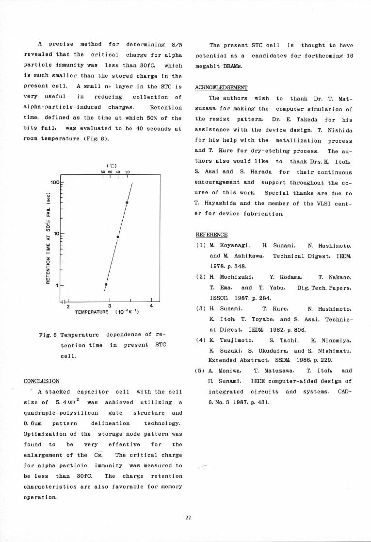
revealed that the critlsal. charge for alphaparticl.e irununlty was less than gOfC, whichis much smaller than the stored charge in thepresent cell. A snall n+ layer in the STC isvery useful in reducing: collection ofalpha-partlcle-induced charges. Retentiontime, def ined as the tirne at which b0% of thebi ts fai 1, was evaluated to be 40 seconds atroom temperature (Fig:. 6).
234TEMPERATURE (10-3K'1)
Fig.6 Temperature dependence of re-
tent i on t irne in Present STC
ce11.
CONCI/USION
- A stacked capacitor cell with the cel1
size of 5.4um' *u" achieved util. izing a
quadruple-polys i 1i con g:ate strueture and
0.6un pattern delineation technol.ogy.
OptinizatTon of the storag:e node pattern was
found to be very effective for the
enlarg:enent of the C;. The critical charg:e
for alpha particle inmunity was measured to
be less than 30f C. The charg:e retent i on
charactdristics are also favorable for memory
ope rat i oru
The present STC cel1 is thought to have
potential as a candidates for forthcoming 16
negabi t DMMs.
ACKNOII,T/EDGEIVIEI'IT
The authors wish to thank Dr. T. Mat-suzawa f or making: the computer simul.ation ofthe resist pattern Dr. E. Takeda for hisassistance with the device desig:n T. Nishidaf or his help wi th the metal.l ization process
and T. Kure for dry-etching process. The au-thors also would like to thank Drs. K Itoh,S. Asai and S. Harada for their continuousencourag:ement and support throughout the co-urse of this worlc Special thanks are due toT. Hayashida and the nember of the VLSI cent-er for device fabricatioru
R,EFERED{CE
( 1) Ut Koyanagl, A Sunami, N. Hashimoto.
and U[ Ashikawa, Technical Dig:est, IEDIU,
1978, p. 348.
(2) H Mochlzuki, Y. Kodama, T. Nakano,
T. Ema, and T. Yabu, Dig. Tectr" Papers,
ISSCC, 1987, p.284.
(8) n Sunami, T. Kure, N. Hashimoto,
K Itotr, T. Toyabe, and S. Asai, Technic-al Dig:est, IEDIVL I9BZ, p. B0O.
(4) K Tsuj imoto, S, Tachi, K Ninomiya,
K Suzuki, S. Okudaira, and S. Nishimatu,D<tended Abstract, ssDIvL 1986, p,229,
(5) A. Moniwa, T. Matuzawa, T. Itoh, and
H Sunami, IEEE computer-aided desig:n of
integ:rated c i rcui ts and systems, CAD-
6, No.8 1987, p.431.
ooIJfi\so\otO
kUJ
=zIFzlrJFlr|E
22