gate – 2015media.careerlauncher.com/gate-exams/gate actual paper...2 solved paper – 2015 (set -...
TRANSCRIPT

Q. No. 1 – 5 Car r y One M ar k Each1. Find the missing sequence in the let ter ser ies
below :
A, CD, GHI , ?, UVWXY
(a) LMN (b) MNO
(c) MNOP (d) NOPQ
2. Choose the cor rect verb to fi l l in the blank below :
Let us .
(a) Introver t (b) alternate
(c) atheist (d) alt ruist
3. Choose the most appropr iate wor d fr om theopt ions given below to complete the fol lowingsentence ?
If the athlete had wanted to come first in the race,he several hours every day.
(a) Should pract ice (b) Should have practised
(c) Pract ised (d) Should be pract icing
4. Choose the most suitable one word subst itute forthe fol lowing expression
Connotat ion of a road or way
(a) Per t inacious (b) Viaticum
(c) Clandest ine (d) Ravenous
5. I f x > y > I , which of the fol lowing must be t rue?
(i ) ln x > ln y (i i ) ex > ey
(i i i ) yx > xy (iv) cos x > cos y
(a) (i ) and (i i ) (b) (i ) and (i i i )
(c) (i i i ) and (i v) (d) (i i ) and (i v)
Q. No. 6 – 10 Car r y Tw o M ar k s Each6. From a circular sheet of paper of radius 30 cm, a
sector of 10% area is removed. I f the remainingpar t is used to make a conical sur face, then theratio of the radius and height of the cone is .
7. I n the fol lowing quest ion, the first and the lastsent ence of t he passage ar e i n or der andnumbered 1 and 6. The rest of the passage is spli tinto 4 par ts and numbered as 2, 3, 4, and 5. These4 par ts are not ar ranged in proper order. Readthe sentences and ar r ange them in a logicalsequence to make a passage and choose thecor rect sequence from the given opt ions.
GENERAL APTI TUDE (GA)
1. One Diwal i , the family r ises ear ly in themorning.
2. The whole family, including the young and theold enjoy doing this,
3. Children let off fireworks later in the nightwith their fr iends.
4. At sunset , the lamps are l i t and the familyper forms var ious r i tuals
5. Father, mother, and chi ldren visit relat ivesand exchange gifts and sweets.
6. Houses look so pret ty with l ighted lamps al laround.
(a) 2, 5, 3, 4 (b) 5, 2, 4, 3
(c) 3, 5, 4, 2 (d) 4, 5, 2, 3
8. Ms. X wil l be in Bagdogra from 01/05/2014 to20/05/2014 and from 22/05/2014 to 31/05/2014. Onthe morning of 21/05/2014, she wil l reach Kochivia Mumbai.
Which one of the statements below is logical lyval i d and can be i n fer r ed f r om t he abovesentences ?
(a) Ms. X wil l be in Kochi for one day, only in May
(b) Ms. X will be in Kochi for only one day in May
(c) Ms. X will be only in Kochi for one day in May
(d) Only Ms. X will be in Kochi for one day in May.
9. log tan 1 + log tan 2 + ..... + log tan 89 is ..........
(a) 1 (b)1
2(c) 0 (d) – 1
10. Ram and Shyam shared a secret and promisedto each other that it would remain between them.Ram expressed himself in one of the fol lowingways as given in the choices below.
Identify the cor rect way as per standard English.
(a) I t would remain between you and me.
(b) I t would remain between I and you
(c) I t would remain between you and I
(d) I t would remain with me.
GATE – 2015EC : EL ECTRONI CS & COM M UNI CATI ON ENGI NEERI NG
Set - 3N o. of Quest i ons : 65 Maxi mum Mar k s : 100
2 SOLVED PAPER – 2015 (SET - 3)
EL ECTRONI CS AND
COM M UNI CATI ON ENGI NEERI NG
Q. No. 1 – 25 Car r y One M ar k Each
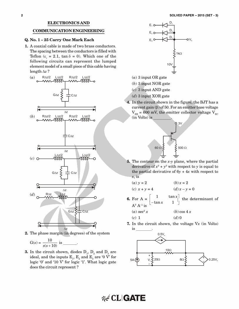
1. A coaxial cable is made of two brass conductors.The spacing between the conductors is fi l led withTeflon (r = 2.1, tan = 0). Which one of thefol lowing ci r cui t s can r epr esent the lumpedelement model of a small piece of this cable havinglength z ?
(a)
C zG z
z
L z/2R z/2 L z/2 R z/2
(b)
C z
z
L z/2R z/2 L z/2 R z/2
(c)
C zG z
L z/2 L z/2
z(d)
C zG z
z
L zR z
2. The phase margin (in degrees) of the system
G(s) = 10
( 10)s s is .
3. I n the circuit shown, diodes D1, D2 and D3 areideal, and the inputs E1, E2 and E3 are ‘0 V’ forlogic ‘0’ and ‘10 V’ for logic ‘1’. What logic gatedoes the circuit represent ?
E1
E2
E3
D1
D2
D3 V0
1k
10V
(a) 3 input OR gate
(b) 3 input NOR gate
(c) 3 input AND gate
(d) 3 input XOR gate
4. I n the circuit shown in the figure, the BJT has acur rent gain () of 50. For an emitter base voltageVEB = 600 mV, the emit ter col lector voltage VEC
(in Volts) is .3V
60 500
5. The contour on the x-y plane, where the par t ialder ivat ive of x2 + y2 with respect to y is equal tothe par t ial der ivat ive of 6y + 4x with respect tox, is
(a) y = 2 (b) x = 2
(c) x + y = 4 (d) x – y = 0
6. For A = 1 tan
tan 1
x
x
the deter minant of
AT A – 1 is
(a) sec2 x (b) cos 4 x
(c) 1 (d) 0
7. I n the circuit shown, the voltage Vx (in Volts)is .
+–85A 20
10
Vx
0.5Vx
0.25Vx
+
–

SOLVED PAPER – 2015 (SET - 3) 3
8. Which one of the fol lowing 8085 microprocessorprograms cor rect ly calculates the product of two8-bi t number s stor ed in r egister s B and C ?(Opt ions)
(a) MVI A, 00 H (b) MVI , A, 00H
JNZ LOOP CMP C
CMP C LOOP DCR B
LOOP DCR B JNZ LOOP
HLT HLT
(c) MVI A, 00H (d) MVI A, 00H
LOOP ADD C ADD C
9. Consider the funct ion g(t) = e– t sin (2t) u(t) whereu(t) is the unit step funct ion. The area under g(t)is .
10. I n the circuit shown using an ideal opamp, the3-dB cut-off frequency (in Hz) is .
10k 10k
10k 10k+
–
Vi
0.1 FV0
11. The modulat i on scheme commonly used fort ransmission from GSM mobile terminals is
(a) 4-QAM
(b) 16-PSK
(c) Walsh-Hadamard or thogonal codes
(d) Gaussian Minimum Shift Keying (GMSK)
12. Which one of the fol lowing processes is prefer redto form the gate dielectr ic (SiO2) of MOSFETs ?
(a) Sputter ing
(b) Molecular beam epitaxy
(c) Wet oxidat ion
(d) Dry oxidat ion
13. Consider the Bode plot shown in figure. Assumethat al l the poles and zeros are real valued.
0 dB
40 dB
fL300
40 dB/dec
900 fH
Freq. (Hz)
–40 dB/dec
The value of fH – fL (in Hz) is .
14. I n the circuit shown, assume that diodes D1 andD2 are ideal. I n the steady-state condit ion theaverage voltage Vab (in Volts) across the 0.5 Fcapacitor is .
+–Vab
b 0.5 F
D2
D1
1 F
50 sin( )t
~
15. The t ransfer funct ion of a first order control ler is
given as GC(s) = K s a
s b
where, K , a and b are
posi t ive r eal numbers. The condi t ion for thiscontrol ler to act as a phase lead compensator is
(a) a < b (b) a > b
(c) K < ab (d) K > ab
16. A message signal m(t) = Am sin(2fmt) is used tomodulate the phase of a car r ier Ac cos(2fct) toget the modulated signal y(t) = Ac cos(2fct + m(t)).The bandwidth of y(t)
(a) depends on Am but not on fm
(b) depends on fm but not on Am
(c) depends on both Am and fm
(d) does not depends on Am or fm
17. The di r ect iv i t y of an antenna ar r ay can beincreased by adding more antenna elements, asa larger number of elements
(a) improves the radiat ion efficiency
(b) increases the effect ive area of the antenna
(c) results in a bet ter impedance matching
(d) al lows more power to be t ransmit ted by theantenna
18. For the circuit shown in the figure, the Theveninequivalent voltage (in Volts) across terminals
a-b is .
a
b
6
3
12V 1A
19. The impulse response of an LTI system can beobtained by
(a) different iat ing the unit ramp response
(b) different iat ing the unit step response
(c) integrat ing the unit ramp response
(d) integrat ing the unit step response
20. Consider a four point moving aver age fi l t er
defined by the equat ion y[n] = 3
0 iin i
The condition on the filter coefficients that resultsin a null at zero frequency is

4 SOLVED PAPER – 2015 (SET - 3)
(a) 1 = 2 = 0; 0 = – 3
(b) 1 = 2 = 1; 0 = – 3
(c) 0 = 3 = 0; 1 = 2
(d) 1 = 2 = 0; 0 = 3
21. I f C is a circle of radius r with centre z0, in thecomplex z-plane and if n is a non-zero integer,
then 1
0
n
dz
z z equals
(a) 2nj (b) 0
(c)2nj
(d) 2n
22. At very high frequencies, the peak output voltageV0 (in Volts) is .
±
1k 1k
100
1k1k
100 FV0
100 F
1.0sin( )Vt
23. I f the base width in a bipolar junct ion t ransistoris doubled, which one of the fol lowing statementswil l be TRUE ?
(a) Cur rent gain wil l increase
(b) Unity gain frequency wil l increase
(c) Emitter base junction capacitance will increase
(d) Ear ly voltage wil l increase
24. The value of 0
12
n
n
n
is .
25. The circuit shown consists of J-K fl ip-flops, each
with an active low asynchronous reset R inputd .The counter cor responding to this circuit is
Rd
1Clock
1
1
1
J Q
K Rd
J Q
K Rd
J Q
K1
1
(a) a modulo-5 binary up counter
(b) a modulo-6 binary down counter
(c) a modulo-5 binary down counter
(d) a modulo-6 binary up counter
Q. No. 26 – 55 Car r y Tw o M ar k s Each
26. A 200 m long transmission line having parametersshown in the figure is terminated into a load RL.The l ine is connected to a 400 V source having
source resistance RS through a switch which isclosed at t = 0. The t ransient response of thecircuit at the input of the l ine (z = 0) is also drawnin the figure. The value of RL (in ) is
r,eff = 2.25
R = 150 S
V = 400VS
R = 500
200mz = Lz = 0
V(0, )t
2.0
62.5V
RL
100V
t( s)
27. A coaxial capacitor of inner radius 1 mm and outerradius 5 mm has a capacitance per unit length of172 pF/m. I f the rat io of outer radius to inner isdoubled, the capacitance per uni t length (inpF/m) is .
28. A universal logic gate can implement any Booleanfunct ion by connect ing sufficient number of themappropr iately. Three gates are shown.
F1 = X + YXY
XY
F2 = X.Y
XY
F3 = X + Y
Which one of the fol lowing statements is TRUE ?
(a) Gate 1 is a universal gate.
(b) Gate 2 is a universal gate.
(c) Gate 3 is a universal gate.
(d) None of the gates shown is a universal gate.
29. The Newton-Raphson method is used to solve theequat ion f(x) = x3 – 5x2 + 6x – 8 = 0. Taking theinit ial guess as x = 5, the solut ion obtained at theend of the first i terat ion is .
30. A random binary wave y(t) is given by
y(t ) = X T .nn
p t n
where p(t) = u(t) – u(t – T), u(t) is the unit stepfunct ion and is an independent random variablewith uniform distr ibution in [0, T]. The sequence{Xn} consist s of i ndependent and ident ical lydist r ibuted binary valued random var iables withP{Xn = +1} = P{Xn = – 1} = 0.5 for each n.
The value of the auto cor relat ion 3TR E
4yy
3T( )
4y t y t
equal .

SOLVED PAPER – 2015 (SET - 3) 5
31. A three bit pseudo random number generator isshown. Init ial ly the value of output Y = Y2 Y1 Y0
is set to 111. The value of output Y after threeclock cycles is
D2
CLK
Q2D1 Qt Q0D0
Y2 Y1 YD
(a) 000 (b) 001
(c) 010 (d) 100
32. I n the circuit shown, assume that the opamp isideal. I f the gain (Vo/V in) is – 12, the value of R(in k) is
V0
R
10k 10k
10kVin
+
–
33. Two sequences x1[n] and x2[n ] have the sameenergy. Suppose x1[n] = 0.5n u[n], where is aposit ive real number and u[n] is the unit stepsequence. Assume
2
1.5 for 0,1
0 otherwise
nx n
Then the value of is .
34. The ABCD parameters of the fol lowing 2-por tnetwork are
(5 + j4) (5 – j4)
(2 + j0)
(a)3.5 2 20.5
20.5 3.5 2
j
j
(b)3.5 2 0.5
0.5 3.5 2
j
j
(c)10 2 0
2 0 10
j
j
(d)7 4 0.5
30.5 7 4
j
j
35. A network is descr ibed by the state model as
1x = 1 22 3x x u
2x = 24x u
y = 1 23 2x x
The t ransfer funct ion H(s) = Y( )U( )
ss
is
(a) 11 35
2 4s
s s
(b)
11 35
2 4s
s s
(c)
11 382 4s
s s
(d)
11 382 4s
s s
36. I n the ci r cui t shown, t he cur r ent I f l owingthrough the 50 resistor will be zero i f the valueof capacitor C (in F) is .
~
1mH
I
50 1mH
1mH C5 sin (5000 ) t
37. A realizat ion of a stable discrete t ime system isshown in figure. I f the system is excited by a unitstep sequence input x[n], the response y[n] is
++
+
5/3–2/9
z–1
z–1
1y n[ ]
–5/3
x n[ ]
(a) 1 24 ( ) 5
3 3
n n
u n u n
(b) 2 15 ( ) 3
3 3
n n
u n u n
(c) 1 25 ( ) 5
3 3
n n
u n u n
(d) 2 15 ( ) 5
3 3
n n
u n u n
38. The complex envelope of the bandpass signal
x(t) = –
sin52 sin ,
45
t
tt
centered about f = 1
Hz,2
is

6 SOLVED PAPER – 2015 (SET - 3)
(a) 4
sin5
5
j
t
et
(b) 4
sin5
5
j
t
et
(c) 4
sin52
5
j
t
et
(d) 4
sin52
5
j
t
et
39. I n the circuit shown, assume that the diodes D1
and D2 are ideal. The average value of voltageVab (in Volts), across terminals ‘a’ and ‘b’ is .
~
Vab
+ –10kD2D1
20k10k6 sin( ) t
40. Consider the different ial equat ion2
2
( ) ( )3 2 ( ) 0.
d x t dx tx t
dt dt
Given x(0) = 20 and x(1) = 10e
,
where e = 2.71. the value of x(2) is .
41. Let 1 cos8n
x n
be per iodic signal with
per iod 16. I ts DFS coefficient ar e defined by
k = 15
0
1exp
16 8x
x n j kn
for al l k. The value
of the coefficient 31 is .
42. A fair die with faces {1, 2, 3, 4, 5, 6} is thrownrepeatedly t i l l ‘3’ is observed for the first t ime.Let X denote the number of t imes the die isthrown. The expected value of X is .
43. The electr ic field profi le in the deplet ion regionof a p-n junct ion in equil ibr ium is shown in thefigure. Which one of the fol lowing statements isNOT TRUE ?
1.00.5 X( m)
E
(V/cm)104
(a) The left side of the junct ion is n-type and ther ight side is p-type
(b) Both the n-type and p-type deplet ion regionsare uniformly doped
(c) The potent ial difference across the deplet ionregion is 700 mV
(d) I f the p-type region has a doping concentrat ionof 1015 cm – 3, then the doping concentrat ion inthe n-type region wil l be 1016 cm – 3
44. A vector field D = 22 a + z az exists inside acyl indr ical region enclosed by the sur faces = 1,z = 0 and z = 5. Let S be the sur face bounding thiscyl indr ical region. The sur face integral of this
field on S D.s
ds is .
45. An npn BJT having reverse saturat ion cur rentI s = 10– 15 A is biased in the forward act ive regionwith VBE = 700 mV. The thermal voltage (VT) is25 mV and the current gain () may vary from 50to 150 due to manufactur ing var iat ions. Themaximum emit ter cur rent (in A) is .
46. Consi der t he 3 m l ong l ossl ess ai r -f i l l edtransmission l ine shown in the figure. I t has acharacter ist ic impedance of 120, is terminatedby a short circuit , and is excited with a frequencyof 37.5 MHz. What is the nature of the inputimpedance (Zin)?
Z = 0L
3mZin
(a) Open (b) Shor t
(c) Inductive (d) Capacit ive
47. The cur rent in an enhancement mode NMOSt r ansi st or bi ased i n sat u r at i on mode wasmeasured to be 1 mA at a drain-source voltage of5 V. When the drain-source voltage was increasedto 6 V while keeping gate-source voltage same,the drain cur rent increased to 1.02 mA. Assumethat drain to source saturat ion voltages is muchsmaller than the applied drain-source voltage.The channel length modulat ion par ameter (in V – 1) is .
48. For the system shown in figure, s = – 2.75 l ies onthe root locus i f K is .
10
Kss + 3 + 2
Y( )s
–
+

SOLVED PAPER – 2015 (SET - 3) 7
49. An SR latch is implemented using TTL gates asshown in the figure. The set and reset pulseinputs ar e pr ovided using t he push-but tonswitches. I t is observed that the circuit fai ls towor k as desi r ed. The SR latch can be madefunct ional by changing
QSet
Reset
5V
Q
(a) NOR gates to NAND gates
(b) inver ters to buffers
(c) NOR gates to NAND gates and inver ters tobuffers
(d) 5 V to ground
50. The var iance of the r andom var iable X withprobabil i ty density funct ion
1( )
2xf x x e is
51. Consider a cont inuous-t ime signal defined as
sin
2 * ( 10 )
2n
t
x t t nt
Where ‘* ’ denotes the convolut ion operat ion andt is in seconds. The Nyquist sampling rate (insamples / sec) for x(t) is .
52. I n the circuit shown, the both the enhancementmode NM OS t r ansist or s have the fol lowingcharacter ist ics : kn = n Cox (W/L ) = 1 mA/V2;VTN = 1V. Assume t hat t he channel l engt hmodulat ion par ameter is zer o and body isshor ted to source. The minimum supply voltageVDD (in volts) needed to ensure that t ransistorM 1 oper ates in saturat ion mode of oper at ionis .
53. The posit ion control of a DC servo-motor is givenin the figure. The values of the parameters areK T = 1 N-m A, Ra = 1 , L a = 0.1H. J = 5 kg-m2,B = 1 N-m (rad/sec) and K b = 1 V/(rad/sec). Thesteady-state posit ion response (in radians) dueto unit impulse disturbance torque Td is .
Kb
KT
R + L Sa a
1JS + B
1S
+–V ( )d s
–+
T ( )a s
( )s
54. The character ist ic equat ion of an LTI system isgiven by F(s) = s5 + 2s4 + 3s3 + 6s2 – 4s – 8 = 0. Thenumber of roots that l ie st r ict ly in the left halfs-plane is .
55. Suppose x[n] is an absolutely summable discrete-t ime signal. I ts z-t ransform is a rational functionwith two poles and two zeroes. The poles are atz = 2j . Which one of the fol lowing statements isTRUE for the signal x[n] ?
(a) I t is a finite durat ion signal.
(b) I t is a causal signal.
(c) I t is a non-causal signal.
(d) I t is a per iodic signal
ANSWERS
GENERAL APTI TUDE
1. (c) 2. (b) 3. (b) 4. (b) 5. (a) 6. (1.9-2.2) 7. (b) 8. (b) 9. (c) 10. (a)
EL ECTRONI CS AND COM M UNI CATI ON ENGI NEERI NG
1. (b) 2. (84.32) 3. (c) 4. (2) 5. (a) 6. (c) 7. (8) 8. (c) 9. (0.155)10. (159.15)
11. (d) 12. (d) 13. (8970) 14. (100) 15. (a) 16. (c) 17. (b) 18. (10) 19. (b) 20. (a)
21. (b) 22. (0.5) 23. (d) 24. (2) 25. (a) 26. (30) 27. (120.22) 28. (c) 29. (4.2903)30. (0.25)
31. (d) 32. (1) 33. (1.49-1.51) 34. (b) 35. (a) 36. (20) 37. (c) 38. (c) 39. (5) 40. (0.8556)
41. (0.5) 42. (6) 43. (c) 44. (78.53) 45. (1475) 46. (d) 47. (0.022) 48. (0.3) 49. (d) 50. (6)
51. (0.4) 52. (3) 53. (– 0.5) 54. (2) 55. (c)
8 SOLVED PAPER – 2015 (SET - 3)
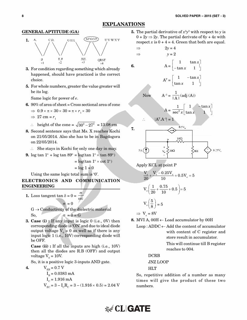
EXPL ANATI ONSGENERAL APTI TUDE (GA)
1.
3. For condit ion regarding something which alreadyhappened, should have pract iced is the cor rectchoice.
5. For whole numbers, greater the value greater willbe i ts log.
Same logic for power of e.
6. 90% of area of sheet = Cross sect ional area of cone
0.9 30 30 = r 1 30 27 cm = r 1
height of the cone = 2 230 27 = 13.08 cm
8. Second sentence says that Ms. X reaches Kochion 21/05/2014. Also she has to be in Bagdogoraon 22/05/2014.
She stays in Kochi for only one day in may.
9. log tan 1 + log tan 89 = log(tan 1 tan 89)
= log(tan 1 cot 1)
= log 1 = 0
Using the same logic total sum is ‘0’.
E L E CT R ON I CS A N D COM M U N I CAT I ONENGI NEERI NG
1. L oss tangent tan = 0 =
= 0G Conduct ivity of the dielectr ic mater ialSo, = 0 = G
3. Case (i ) : I f any input is logic 0 (i .e., 0V) thencorresponding diode is ‘ON’ and due to ideal diodeoutput voltage V0 = 0 as well as i f there is anyinput logic 1 (i .e., 10V) cor responding diode wil lbe OFF.Case (i i ) : I f al l the inputs are high (i .e., 10V)then al l the diodes are R.B (OFF) and outputvoltage V0 = 10V.So, i t is a posit ive logic 3-inputs AND gate.
4. VEB = 0.7 VI B = 0.0383 mAI C = 1.916 mA
VEC = 3 – I CRC = 3 – (1.916 0.5) = 2.04 V
5. The par t ial der ivat ive of x2y2 with respect to y is0 + 2y 2y. The par t ial der ivate of 6y + 4x withrespect x is 0 + 4 = 4. Green that both are equal. 2y = 4 y = 2
6. A = 1 tan
tan 1
x
x
AT = 1 tan
tan 1
x
x
Now A – 1 = 1
| A |(adj (A))
A = 2
1 tan1sec tan 1
xx x
AT.A – 1 = 1
7.
Apply KCL at point P
V V 0.25V0.5V 5
20 10x x x
x
1 0.75V 0.5 5
20 10x
5V
8x
= 5
Vx = 8V
8. MVI A, 00H Load accumulator by 00H
Loop : ADDC Add the content of accumulatorwith content of C register andstore result in accumulator.
This wil l cont inue t i l l B registerreaches to 004.
DCRB
JNZ LOOP
HLT
So, r epet i t ive addit ion of a number as manyt i mes w i l l gi ve t he pr oduct of t hese t wonumbers.

SOLVED PAPER – 2015 (SET - 3) 9
9. g(t) = e– t sin(2t).u(t)
Let y(t) = sin(2t).u(t)
then Y(s) = 2 2
2(2 )s
g(t) = e– 1y(t)
G(s) = Y(s + 1)
G(s) = 2 2
2( 1) (2 )s
G(s) = ( ). stg t e dt
G(0) = ( ).g t dt
Area under g(t ) = 2
21 (2 )
=
6.280.155
40.438
10. f3dB = 1
2 RC
= 3 6
12 10 10 0.1 10
= 159.15 Hz
13. 40 = 10 10 L
40 0log (300) log ( )f
10L
300log
f
= 1
300 = 10 fL
fL = 30 Hz ...(i)
– 40 = 10 H
0 40log log(900)f
H10log
900f
= 1
fH = 900 10 = 9000 ...(i i )fH – fL = 9000 – 30 = 8970 Hz
15. For phase lead compensator
16. y(t) = Ac cos[2fct + m(t)]m(t) = Amsin(2fmt)
Since y(t) is phase modulated signal,(t ) = 2fct + m(t)
Bandwidth = 2[f + fm]
f = 1
( )2
dm t
dt f depends on A m as wel l as f m. Thus
Bandwidth depends on both Am and fm.
17. D = 2
4Ae
D Ae
18.
Apply nodal equat ion at point P1 13 6nV
= 121
3
V2
n = 5
V+n = 10 V
19. Let h(t) be the impulse response of the system
( )( ) ( )h tu t y t
y(t) is unit step response of the system
y(t) = ( )t
h d
I f we need to get h(t), then we have to differentiatey(t).Thus different iat ing the unit -step response givesimpulse response for LTI system.
20. Given y[n] = 2
0
( )ii
x n i
y[n] = 0x[n] + 1x[n – 1] + 2x[n – 2]
+ 3x[n – 3]
Getting a null at zero frequency implies that givenfi l ter can be high pass fi l ter but i t cannot be lowpass fi l ter.H igh pass fi l ter is possible i f we have negat ivecoefficients.Let say, 1 = 2 = 0, 0 = – 3
y[n] = – 3x[n] + a3x[n – 3]H(z) = – 3[1 – z– 3]
H(ej) = – 3[1 – e– j3]
=
3 33 2 22
3 22
j jj e ee j
j
= 32
3
32 sin .
2
jj e
= 32 2
3
32.sin . .
2
j je e
H(ej)= 0 = 0In other cases it in not possible.
10 SOLVED PAPER – 2015 (SET - 3)
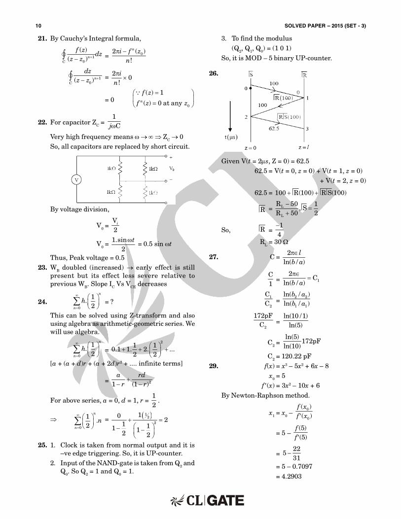
21. By Cauchy’s Integral formula,
10C
( )( )n
f zdz
z z = 02 ( )!
ni f zn
10C ( )n
dzz z = 2
0!i
n
= 00
( ) 1
( ) 0 at anyn
f z
f z z
22. For capacitor ZC = 1Cj
Very high frequency means ZC 0So, al l capacitors are replaced by shor t circuit .
By voltage division,
V0 = V2
i
V0 = 1.sin
2t
= 0.5 sin t
Thus, Peak voltage = 0.523. WB doubled (increased) ear ly effect is st i l l
pr esent but i t s effect less sever e r elat ive toprevious WB. Slope I C Vs VCE decreases
24.0
1.
2
n
n
h
= ?
This can be solved using Z-t ransform and alsousing algebra as ar ithmet ic-geometr ic ser ies. Wewil l use algebra.
0
1.
2
n
n
h
= 2
1 10.1 1. 2. ...
2 2
[a + (a + d)r + (a + 2d)r 2 + .... infinite terms]
= 21 (1 )a rd
r r
For above ser ies, a = 0, d = 1, r = 12
.
0
1.
2
n
n
n
= 12
2
102
1 11 12 2
25. 1. Clock is taken from normal output and it is– ve edge t r igger ing. So, i t is UP-counter.
2. Input of the NAND-gate is taken from Q2 andQ0. So Q2 = 1 and Q0 = 1.
3. To find the modulus(Q2, Q1, Q0) = (1 0 1)
So, i t is MOD – 5 binary UP-counter.
26.
Given V(t = 2s, Z = 0) = 62.562.5 = V(t = 0, z = 0) + V(t = 1, z = 0)
+ V(t = 2, z = 0)
62.5 = 100 R(100) R S(100)
R = L
L
R 50 1, S
R 50 2
So, R = 1
4
RL = 30
27. C = 2
ln( / )l
b a
C1
= 1
2C
ln( / )b a
1
2
CC =
2 2
1 1
ln( / )ln( / )
b ab a
2
172pFC =
ln(10 /1)ln(5)
C2 = ln(5)
172pFln(10)
C2 = 120.22 pF29. f(x) = x3 – 5x2 + 6x – 8
x0 = 5f (x) = 3x2 – 10x + 6
By Newton-Raphson method.
x1 = x0 – 0
0
( )( )
f xf x
= 5 – (5)(5)
ff
= 22
531
= 5 – 0.7097
= 4.2903

SOLVED PAPER – 2015 (SET - 3) 11
30. y(t) = X P( T )nn
t n
Ryy(z) = 1T
Der ivat ion of above autocor relat ion funct ion canbe found in any book deal ing wi th r andomprocess.[B.P. Lathi, Simon, Haykin, Schaum ser ies].
3TR
4yy
= 3 / 4
1
= 14
= 0.25
31. D (Q Q )1 2 0 D (Q )21 D (Q )10 Y (Q )22 Q (Y )11 Q Y01
–
0
01
–
1
00
–
1
10
1
0
01
1
1
00
1
1
10
1 clcokst
2 clcoknd
3 clcokrd
After three clock pulses output Y2Y1Y0 = 100
34. For the standard ‘T’ network, obtain the Z-matr ixfirst and then conver t i t into T-matr ix
Z = 7 4 2
2 7 4
j
j
Z = [(7 + j4)(7 – j4)] – 4= 49 + 16 – 4 = 16
A = 11
21
ZZ =
7 42
j = 3.5 + j2
B = 21
ZZ
= 612
= 30.5
C = 21
1Z =
12
= 0.5
D = 22
21
Z 7 4Z 2
j = 3.5 – j2
T = 3.5 2 30.5
0.5 3.5 2
j
j
35. A = 2 1
0 4
B = 3
1
C = [3 – 2]
H(s) = C(sI – A)– 1B
= 2 1 3[3 – 2]
0 4 1
s
s
= 4 1 31
[3 – 2]( 2)( 4) 0 2 1
ss s s
= 2
3 12 11[3 – 2]
2 8 2
ss s s
= 95 39 25 4( 2)( 4)s s
= 11 35( 2)( 4)
ss s
36.
I f I = 0,Vp = V i,
1 1V
15 55000C
i j j
= 0
15j
= 1
15
5000Cj
= 0
15
=
11
55000C
5 = 1
55000C
1
5000C = 10
C = 4
15 10 = 20 F
37.
From the graph
v[n] = 2
[ ] [ 1] [ 2]9
x n v n v n
y[n] = 5 5
[ 1] [ 2]3 3
v n v n
V(z) = 1 22
1 X( )9
z z z
V( )X( )
zz
= 1 2
12
19
z z ...(i)
Y( )V( )
zz
= 1 25 53 3
z z ...(i i )
Mult iplying (i ) and (i i ) we get
Y( )X( )
zz
=
1 1
1 2
5[1 ]
32
19
z z
z z

12 SOLVED PAPER – 2015 (SET - 3)
For unit step response,
X(z) = 1
11 z
Y(z) =
1
1 2
53
21
9
z
z z
= 1 1
A B1 2
1 13 3
z z
On solving,A = 5; B = – 5
y[n] = 1 2
5 [ ] 5 [ ]3 3
n n
u n u n
38. x(t) = sin( / 5)
2 sin/ 5 4t
tt
we can wr ite above expression as
x(t) = – sin( / 5)2 cos sin sin cos
/ 5 4 4t
t tt
= sin( / 5) sin( / 5)
cos sin( )/ 5 ( / 5)t t
t tt t
Alsox(t) = xc(t) cos 2fct – xs(t) sin (2fct)
[Low pass representat ion of Bandpass signals]
xc(t) =sin( / 5)
/ 5t
t
xs(t) =sin( / 5)
/ 5t
t
xce(t) is the complex envelope of x(t)
xce(t) = xc(t) + jxs(t)
=sin( / 5)
/ 5t
t
[1 + j ]
= / 42 sin( / 5)( / 5)
jte
t
40. Given 2
2
( ) 3 ( )2 ( ) 0
d x t dx tx t
dt dt
x(0) = 20
x(1) = 10e
x(2) = ------
Auxil lary equat ion ism2 + 3m + 2 = 0
m = 1, – 2Complementary solut ion xe = c1e
– t + c2e– 2t
Par t icular solut ion xp = 0
Finally x = xc + xp = c1e– t + c2e
– 2t
x(0) = 20
20 = c1 + c2 (a)
x(1) = 10e
10e
= c1e– 1 + c2e
– 2
10 = c1 + c2e– 1 (b)
From (a) c1 = 20 – c2
Now 10 = (20 – c2) + c2e– 1
10 = c2(e– 1 – 1) + 20
c2 = 1
10 201e
= – 1
101e
= 1
101 e
= 10
1e
e
c1 = 10
201e
e
= 20 20 10
1e e
e
= 10 20
1ee
x(t) = 1 210 20 101 1
te ee e
e e
x(2) =
2
410 20 101 1
ee e
ee e
= 0.8556
41. x[n] = 1 + cos 8n
N = 16
x[n] = 2 216 161 1
12 2
n nj j
e e
a– 1 = 12
, a1 = 12
, a0 = 1
a1 = a– 1 + 16
a– 1 = a15 = 12
a0 = 1, a1 = 1L
, a2 to a14 = 0, a15 = 12
DFS coefficients are also per iodic with per iod 16.
a31 = a16 + 15
a31 = a15
a31 = 12

SOLVED PAPER – 2015 (SET - 3) 13
43. Built in potent ial
o = 6 61 V10 (1.1 10 )2
mm
= 0.55 voltsBut in Quest ion (opt ion (c)) is given as 700 mV.
44. D = 22a + zaz
ZD.ds =
V( .D)dv
.D = D1 1 D
( D ) z
z
= 21( 2 ) 0 1
= 212(3) 1
= 6 + 1
V( .D)dv =
1
02
0
5
0(6 1)
zd d dz
= 1
3 2
0
6(2 )(5)
3 2
= 1
2 102
V( .D)dv = 78.53
45. I B = CI
= VBE
VTSIe
I E = ( + 1)I B
= VBE
VTS
1I .e
=
3
3700 10
9 6 25 10(1.02)(10 10 )e
= 1475 A46. Zin = JZ0 tan l
l = 2
.l
8
6
3 1037.5 10
= 2
(3)8
= 8
= 34
Shor t circuited l ine
0 < l < 2
I nductor
2
< l < Capacitor
47. NMOS SATURATIONI D = 1mA @ VDS = 5V
I D = 1.02mA @ VDS = 6VI D Sat << VDS
I D = k(VGS – VT)2 (1 + VDS)
I D = k(1 + VDS)
10– 3 = k(1 + 5)1.02 10– 3 = k(1 + 6)
1.02 = 1 61 5
1.02 + 5.1 = 1 + 60.02 = 0.9
= 0.022 V – 1
48.
G(s)H(s) = 10 ( 3)( 2)k ss
= ( 3)( 2)
k ss
For k k = Poles lengthzero length
= 0.750.25
= 3
10k = 3k = 0.3
50. Var(x) = E(x2) – (E(x))2
E(x) = | |1.2
xx x e dx
= 0 2 2
0
1 1.
2 2x xx e dx x e dx
= 0
E(x)2 = 2 | |1.2
xx x e dx
= 2
0
12 . .
2xx x e dx
= 3
0. xx e dx
= 3 2
0 0 00
. (3 )( ) 6 ( ) 61
xx x xe
x x e x e e
= 6 Var(x) = 6 – 0 = 6

14 SOLVED PAPER – 2015 (SET - 3)
51. x(t) = sin( / 2)
* ( 10 )( / 2) n
tt n
t
Convol u t i on i n t i me domai n becomesmult ipl icat ion in frequency domain.
1( )
10 sn
f kf
Fs = 1Ts
= 0.1
sin( / 2)( / 2)
tt
( 10 )n
t n
Mult ipl icat ion in frequency domain wil l resultmaximum frequency is 0.2.
Thus Nyquist rate= 0.4 samples/sec
52.
Lower t ransistor (M 1) to work in saturat ionVDS1 VGS1 – V+
So, for minimum VDD
VDS1 = VGS1 – V+
VDS1 = 2 – 1 = 1VVDS1 = VD1 – VS1
1V = VD1 – 0
VD1 = 1V
and I D1 = K (VGS1 – V+)2
VD1 = 2
1 mAV
(2 – 1)2 = 1 mA
Now transistor M 2, VDG = 0VSo, i t wi l l work into saturat ion region and samecur rent wil l flow
I D2 = I D1 = K (VGS2 – V+)2
1 mA = 2
1 mAV
(VDD– 1– 1)2S2 D1( V = V )
VDD = 3V53. Td(s) = 1
(s) = T
1K K
(J B)R L
b
a a
s ss
Steady State Value is 0
l im ( ) 0.5s
s s
54. 55 + 2s4 + 3s3 + 6s2 – 4s – 8 = 05
4
3
2
1
0
1 3 4
S 2 6 8S 8 12 0S 3 8 0
S 9.33 0 0S 8
S
as 0
2s4 + 6s2 – 8 = 0
Let x = s2, then2x2 + 6x – 8
x = 1, – 4
s2 = 1, – 4 s = 1, 2Lies on RHS s = 1, 2There are only two poles on LHS.
55. Since x[n] in absolutely summable thus i ts ROCmust include unit circle.
Thus ROC must be inside the circl ing radius 2.x[n] must be a non-causal signal.