gaasi_bix light emitting diodes - circle - university of british
TRANSCRIPT

GaAsi_Bix Light EmittingDiodes
A New Long Wavelength Semiconductor LightSource
by
Ryan B. Lewis
B .Sc., Daihousie University, 2006
A THESIS SUBMITTED IN PARTIAL FULFILMENT OFTHE REQUIREMENTS FOR THE DEGREE OF
Master of Applied Science
in
The Faculty of Graduate Studies
(Engineering Physics)
The University Of British Columbia
(Vancouver)
October, 2008
© Ryan B. Lewis 2008

Abstract
GaAs1_Bi is an exciting new semiconductor material, which has been pro
posed as a new material for infrared light emitting devices. Recent ad
vancements in the growth of GaAsi_Bi films have made it possible to
produce GaAsi_Bi light emitting diodes for the first time. Throughout
this research we have grown, fabricated and characterized GaAsi_Bi light
emitting diodes. Similarly structured InGai_As light emitting diodes were
also produced and characterized for comparison to the GaAsi_Bi devices.
Strong electroluminescence was obtained from GaAs1_Bi devices, show
ing two emission peaks, one corresponding to the GaAs1_Bi layer and the
other to the GaAs cladding. Emission from InGai_As devices was about
100 times brighter than from GaAsi_Bi devices.
Temperature dependent electroluminescence and photoluminescence mea
surements of a GaAs1_Bi light emitting diode were made and showed some
unusual results. The wavelength of the peak in the electroluminescence from
the GaAs1_Bi was independent of temperature in the range 100 K to 300 K
while the GaAs peak shifted with temperature as expected. Photolumines
cence measurements on the same structure show temperature dependence of
the peak wavelength similar to the temperature dependence of GaAs.
II

Table of Contents
Abstract ii
Table of Contents iii
List of Tables v
List of Figures vi
Acknowledgements ix
1 Introduction 1
2 Growth and Properties of the GaAs1_Bi Alloy 8
2.1 Molecular Beam Epitaxy Growth of GaAs Alloys 8
2.2 Growth of the GaAsi_Bi Alloy 9
2.3 Doping and the p-n Junction Diode 12
2.4 Heterostructure Design 15
2.5 Light Emitting Diode Growth and Characterization 16
3 Post-Growth Fabrication of Light Emitting Diodes 25
3.1 Ohmic Contacts 25
3.2 Mesa Etching 30
111

Table of Contents
4 Electrical Characterization 32
4.1 Current-Voltage Measurements of GaAs1_Bi Diodes . . . . 32
4.2 Current-Voltage Measurements of InGa1_As Diodes . . . . 36
5 Optical Characterization 38
5.1 Electroluminescence (EL) and Photoluminescence (PL) . . 38
5.2 Photoluminescence Measurements 41
5.3 Electroluminescence Measurements 43
5.4 Temperature Dependent Electroluminescence 49
6 Conclusion 52
6.1 Future Work 53
Bibliography 54
iv

List of Tables
2.1 Light Emitting Diode Growths 23
2.2 Selected Light Emitting Diode growth conditions 24
V

List of Figures
1.1 Energy bandgap vs. lattice constant for several semiconductor
alloys[1] 3
1.2 Energy bandgap vs. lattice constant for several semiconductor
alloys including the GaAs-GaN and GaAs-GaBi systems. . . S
1.3 The section of the periodic table containing elements used in
common semiconductors 6
2.1 [004] X-ray rocking curves for three GaAsi_Bi epilayers. A
fit to each curve is shown with dotted lines[2] 11
2.2 Schematic diagram p-n junction at equilibrium (no applied bias). 14
2.3 Schematic diagram of a forward biased p-n junction 15
2.4 [004] rocking curve of a GaAsi_Bi LED sample (r1965) con
taining 1.89’o bismuth. A fit to the data is shown in red . . . . 19
2.5 [004] rocking curves for two GaAsi_Bi LED samples (r1895
and r1917) containing 0.9% and 5.5% bismuth shown in red
and blue 20
2.6 [004] rocking curve of a InGa1_As LED sample (r1929) con
taining 18% indium. A fit to the data is shown in red 21
vi

List of Figures
3.1 Schematic diagram of a metal to n-type semiconductor inter
face in the absence of surface states 27
3.2 Schematic diagram of a metal to n-type semiconductor inter
face with surface states 28
3.3 Schematic of an LED chip after metalization and etching.
Typical thickness for i-GaAs layers was 25 nm, typical GaAsBi
QW thicknesses were 30 nm to 50 nm and typical p-GaAs
thickness was 1 /mum. The top 300 nm of the p-GaAs layer
was removed by etching 31
4.1 Current-Voltage curves for four GaAsi_Bi light emitting diodes
at 300 K. The red line indicates a fit to the data with n = 2.26
ideality factor 33
4.2 Current-Voltage curves for GaAsi_Bi LED r1895. Hollow
data points (low leakage values on reverse bias) correspond to
dots from an unetched device fabricated soon after growth.
Solid data points (high leakage) correspond to measurements
made on the same sample 2 months later, with and without
dipping the sample in HC1 to remove possible oxide and also
for a new device fabricated from the wafer with etched mesas
(solid pink triangles) 35
4.3 Current-Voltage curves for InGai_As LEDs from sample r1929 37
5.1 Possible non-radiative transitions in semiconductors 41
vii

List of Figures
5.2 Photoluminescence spectra for GaAsi_Bi LED structure r1965
over a temperature range of 8 K to 300 K. The inset shows the
peak emission energies as a function of temperature for both
the GaAs and GaAsi_Bi peaks. A fit to the data using the
Varshni equation is also shown (dashed line) 42
5.3 Electroluminescence spectra for a GaAsi_Bi light emitting
diode from sample r1965 for various injection current densities
at 300 K. Room temperature photoluminescence is shown for
comparison 44
5.4 Room temperature electroluminescence spectra from three GaAsi_Bi
LEDs at 100 A/cm2 injection current. The black and red spec
tra were fabricated from growth r1895 and contain 1% bis
muth. The blue spectra (from r1917) contained 5.59’o bismuth
in the GaAsi_Bi layer 47
5.5 Room temperature electroluminescence spectra for an InGai_As
light emitting diode for various injection current densities. 48
5.6 Electroluminescence spectra from GaAsBi LED r1965 at 50 A/cm2
injection current density for temperatures ranging from 100 K
to 300 K 50
viii

Acknowledgements
I would like to thanks my supervisor Tom Tiedje for his inspiration, guidance
and for sharing so much of his knowledge and experience with me. Thanks
to the rest of the MBE group of being so willing to help me out and for being
and so entertaining. Special thanks to Dan Beaton for growing my samples
and for helping me with latex, without you this would have been a short
thesis.
I’d also like to thank my parents for keeping in such close contact and
for providing so much support and encouragement. Thanks to Jeff Dahn at
Dalhousie for encouraging me to continue my academic careere in condensed
matter physics. And of course thanks to Dayna for putting up with me and
cheering me up while I was writing this thesis. Your support has meant so
much.
ix

Chapter 1
Introduction
It is hard to imagine a world without semiconductors. These special mate
rials, group IV alloys, 111-V alloys, Il-VI alloys and recently I-Ill-VT2 alloys
are an integral part of the technology-driven world that we live in. The Ill-V
class of semiconductors dominate applications for the microwave frequency
integrated circuits used in cell phones, light emitting diodes (LEDs), diode
lasers for data transmission, reading and recording for DVD and CD players
and high efficiency solar cells. ITT-V’s are ideally suited for optical appli
cations because their direct bandgap allows for very efficient generation of
light.
GaAs and InP are arguably the most important Ill-V semiconductors.
InP-based lasers are extensively used in fiber optic data transmission. GaAs
has a high electron mobility, good for making high frequency transistors, it
also has a higher breakdown voltage than silicon, allowing for higher power
devices to be made. Despite these advantages, silicon is much more used
for integrated circuit manufacturing. Reasons for this are that: silicon is
more abundant and easier to process; silicon dioxide, which is one of the
best known insulators is easily incorporated into silicon circuits; the higher
hole mobility of silicon allows for fabrication of faster p-channel field effect
transistors, required for complementary metal-oxide-semiconductor (CMOS)
1

Chapter 1. Introduction
logic, which makes GaAs-based logic circuits have much higher power con
sumption. The biggest advantage of GaAs is that it can be easily alloyed with
other ITT-V systems to achieve a wide range of bandgap energies, which allows
for easy fabrication of double heterostructures (DH’s). DHs are formed by
sandwiching a low bandgap semiconductor material between a semiconductor
with a higher bandgap. This structure is extremely usefull for optoelectronic
devices.
The ability to grow high quality films with energy bandgaps lower than
the 1.42 eV GaAs bandgap on GaAs substrates is of much interest for device
applications. The silica fibers used for optical data transmission have no
dispersion at 1.3 tm and are most transparent at 1.55 jim, which correspond
to bandgaps of 0.83 eV and 0.80 eV. The solar cell industry would also like to
grow a 1.0 eV material on GaAs for use in high-efficiency multi-junction solar
cells, thus much effort has been made in developing such materials. Common
bandgap lowering materials used to alloy with GaAs are InAs and GaSb,
however because indium is larger than gallium and antimony is larger than
arsenic TnGai_As and GaAsi_Sb alloys have a larger lattice constants
than pure GaAs. This limits the thickness and compositions that can be
grown pseudomorphically on GaAs before the strain causes dislocations to
form. Fig. 1.1 shows the energy bandgap as a function of lattice constant
for several semiconductor alloys, including the GaAs-InAs and GaAs-GaSb
alloys.
The heaviest group III and V elements, thorium and bismuth have been
largely neglected as candidates for alloying with GaAs. These elements are
difficult to incorporate into the lattice due to their large size and tendency
2

Chapter 1. Introduction
This figure has been removed due to copyright restrictions. The figure
showed a plot of the bandgap of several semiconductor alloys as a function
of lattice constant and was obtained from [1].
Figure 1.1: Energy bandgap vs. lattice constant for several semiconductor
alloys[1].
to surface segregate[3j [4]. First reports of bismuth incorporation into GaAs
came from metal-organic vapor phase epitaxy (MOVPE) in 1998 from Oe
and Okamoto, who were able to grow GaAsi_Bi with concentrations up
to x = O.02[5]. Molecular beam epitaxy (MBE) growth was first presented
5 years later[4][6]. Incorporation of small amounts of bismuth produces a
large reduction in the bandgap of GaAs[7]; 88 meV per percent bismuth,
which is seven and four times greater than what is achievable with indium
or antimony respectively[8] for equal incorporated amounts.
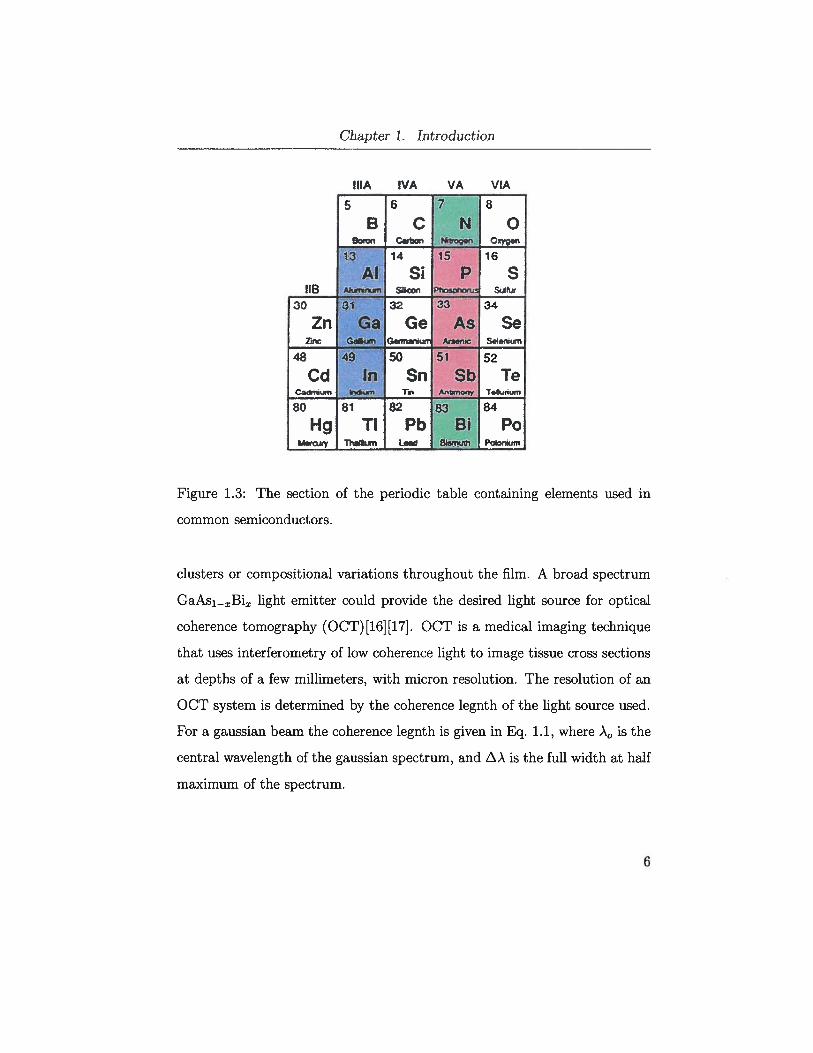
The portion of the periodic table, corresponding to elements found in
semiconductors is shown in Fig. 1.3. The red and blue elements can be de
scribed as alloying elements with GaAs, while the green elements: nitrogen
and bismuth seem to behave more like impurities when incorporated, rather
3

Chapter 1. Introduction
than forming an alloy. The two ternary alloys GaNAsi_ and GaAsj_Bi
are complimentary in that GaNAs1_reduces the bandgap by lowering the
conduction band minimum (CBM), while GaAsi_Bi lowers the bandgap by
raising the valence band maximum (VBM) [8]. In the GaAsi_Bi alloy, the
Bi6p level is resonant with the VBM[9], whereas in the case of the GaNAsi_
alloy, the N2p levels are deep in the valence band and the unoccupied N2s
antibonding orbital is resonant with the CBM[10j. Since nitrogen incorpora
tion decreases the GaAs lattice size and bismuth increases it, the quaternary
GaNAsi_Bi alloy has been proposed as strain compensating alloy, allowing
low bandgap GaNAsi_Bi to be lattice matched to GaAs[11]. Fig. 1.2 shows
the energy bandgap vs. lattice constant for selected 111-V semiconductor al
loys, including the GaAs-GaN system and the GaAs-GaBi system. The blue
line corresponds to the GaAs-GaBi alloy.
Most properties, including bandgap to a first approximation follow Veg
ard’s law[12] when alloying ITT-V semiconductors, however this is not true for
the incorporation of nitrogen. For example, the bandgap of GaN is higher
than bandgap of GaAs, however incorporation of small amounts of nitrogen
into the GaAs lattice results in a reduction of the GaAs bandgap by the
huge amount of 200 meV per percent nitrogen[13][14]. GaBi has not been
synthesized, so it’s lattice constant and bandgap have only been determined
theoretically by density functional theory.
It has been proposed that GaAsi_Bi alloys have an anomalously tem
perature insensitive bandgap[4]. The temperature dependence of the GaAsi_Bi
bandgap has recently been measured, however quite different values were
obtained[5] [6] [15]. Photoluminescence and photoreflectance measurements
4

Chapter 1. Introduction
Figure 1.2: Energy bandgap vs. lattice constant for several semiconductor
alloys including the GaAs-GaN and GaAs-GaBi systems.
on a sample containing 2.6% bismuth by Yoshida, et al. found the temper
ature dependence of the GaAs1_Bi bandgap to be 1/3 that of GaAs[5],
however other measurements found a similar temperature dependence to
GaAs [6]
As the heaviest non-radioactive element, bismuth alloying creates an un
usually large spin orbit splitting. Incorporation of bismuth into Ill/V alloys
could provide the large spin-orbit coupling needed for spintronic devices.
The GaAsi_Bi alloy has recently been shown to have very wide photo-
luminescence (Pb) spectra, suggesting the grown films may contain bismuth
4
3
04.0 5.0 5.5 6.0
Lattice Constant (A)
5
Chapter 1. Introduction
Figure 1.3: The section of the periodic table containing elements used in
common semiconductors.
clusters or compositional variations throughout the film. A broad spectrum
GaAsi_rBi,, light emitter could provide the desired light source for optical
coherence tomography (OCT) [16] [17]. OCT is a medical imaging technique
that uses interferometry of low coherence light to image tissue cross sections
at depths of a few millimeters, with micron resolution. The resolution of an
OCT system is determined by the coherence legnth of the light source used.
For a gaussian beam the coherence legnth is given in Eq. 1.1, where )*-, is the
central wavelength of the gaussian spectrum, and LS\ is the full width at half
maximum of the spectrum.
lilA IVA VA VIA
5 6 7 8
B CN 08oron Caton gen. Ozygen
13 14 15
Al SIP118 AIMiimXn n PtIOSphOU
16
S
30 31 32 33 34
Zn:
Ge As SeZinc Gai G.mainr ksnc Seeium
48 50 51 52
Cd In Sn Sb TeCad Th Anniony T.aunum
80 81 82 83 84
Hg TI Pb Bi Po&4.ai.y fl*bsn L. BnIUth Poonk,m
6

Chapter 1. Introduction
(1.1)
For maximum imaging depth the light source must operate in the near
infrared range ( 850 — 1300 nm) where tissue is most transparent. These
demands perfectly overlap with the characteristics of the GaAsi_Bi alloy,
thus OCT is a very promising application of a GaAsi_Bi light emitters.
Throughout this research we have fabricated and characterized GaAsi_Bi
light emitting diodes. To our knowledge, these results represent the first
GaAsi_Bi LEDs ever made. We discuss in detail the growth and fab
rication processes that we have developed. Current-Voltage, temperature
dependent photoluminescence and electroluminescence results are also pre
sented and discussed for this exciting new semiconductor.
7

Chapter 2
Growth and Properties of the
GaAsi_Bi Alloy
2.1 Molecular Beam Epitaxy Growth of
GaAs Alloys
Gallium Arsenide is probably the most important material for solid state
light emitting devices. GaAs is advantageous because of it’s high electron
mobility, ease of manufacturing, availability of 150 mm wafers and ability
to be alloyed with other elements to modify the GaAs bandgap. GaAs, as
many 111-V semiconductors has a direct bandgap, allowing for much more
efficient optical devices to be made, compared to elemental semiconductors
like silicon and germanium. The direct bandgap means transitions between
the conduction band minimum (CBM) and valance band maximum (VBM)
can occur without either the absorption or emission of phonons, to conserve
momentum.
Molecular beam epitaxy (MBE) is a common method for the preparation
of GaAs based semiconductor materials in thin film form. MBE is a process,
where beams of atoms or molecules (usually from thermal evaporation) are
8

Chapter 2. Growth and Properties of the GaAsi_Bi Alloy
simultaneously incident on a heated substrate in ultra-high vacuum (UHV).
Individual beams can be turned off or on in a fraction of a second by the use
of shutters. This process allows for precise control of compositions and layer
thicknesses on the sub-monolayer scale and the ability to abruptly change the
composition of the layer being grown. Typically, GaAs is grown at rates of
about 1 pm per hour at temperatures of about half the melting point of GaAs
or 500°C to 650°C. The fact that growth takes place so much colder than
the melting point allows for metastable compounds, not found in nature to
be created. Low temperature also minimizes the number of thermodynamic
defects in the grown material.
2.2 Growth of the GaAsi_Bi Alloy
Under normal GaAs growth conditions, bismuth tends to surface segregate
and does not incorporate into the GaAs lattice. At these conditions bismuth
behaves as an ideal surfactant, as it does not incorporate. Bismuth has been
used as a surfactant in the growth of several GaAs-based material systems,
such as GaAs and InGai_As where it has been shown to improve surface
smoothness and photoluminescence [18] [19] [7 ]. In the case of GaNAs1_
and InGaNAsi_ it has been shown to result in smoother surfaces, enhanced
nitrogen incorporation, and increases photoluminescence by reducing defects
[3][19j.
Incorporation of bismuth into the GaAs lattice requires atypical growth
condidions, to reduce the tendency of bismuth to surface segregate and re
duce the competition for group V sites. To achieve this, low growth temper
9

Chapter 2. Growth and Properties of the GaAs1_Bi Alloy
atures and low V:III ratios (usually 1:1 to 4:1 compared to typical ratios of
about 10:1) are required. High bismuth incorporation of up to 10% has been
achieved in the temperature range of 270°C-320°C[1]. Low growth rates of
about (1 nm/mm) are used in order to have more control over the excess
bismuth on the surface and minimize the likelihood of bismuth accumula
tion in the form of droplets[1]. Droplets are very undersirable as they lead
to local variations in the amount of bismuth coverage and hence the local
composition. Droplets also increase the surface roughness. In the case of
low growth rates, the rate of bismuth incorporation is less, so lower bismuth
fluxes can be used. In this case most of the incident bismuth flux is evap
orated, rather than incorporated, thus allowing for more control over the
amount of surface bismuth present. Low temperature growth also leads to
a larger critical thickness before dislocations form[1], which allows for high
strain, small bandgap, epi-layers to be grown on GaAs without relaxation.
Fig. 2.1 shows [004] X-ray rocking curves for three GaAsi_Bi epilay
ers for x values of 1.4%, 5% and 10%[1]. Fits to each data set are shown
as dotted lines. The sharp peak in each spectra corresponds to the [004]
GaAs substrate peak and the smaller satelite peak on the left corresponds
to the GaAsi_Bi epilayer. Dampled pendellosung fringes are visible in
all the curves, indicating high structural quality. These interference fringes
also allow for determination of layer thicknesses. Composition is determined
from the separation in epilayer and substrate peaks using the known shift
of 300 arcsec per percent bismuth incorporation in the [004] X-ray peak for
incorporation up to a few percent. The shift in lattice constant with bismuth
has been determined by comparing Rutherford backscattering (RBS) compo
10

Chapter 2. Growth and Properties of the GaAs1_Bi Alloy
sitional data to X-ray diffraction data on samples with up to 3.1% bismuth by
Tixier et al. [3]. Since the lattice constant of zincblend GaBi is unknown, one
could not use Vegard’s law to determine composition from X-ray data alone,
however the work by Tixier et al. has provided a theoretical prediction of
the GaBi lattice constant of 0.6336 nm based on an extrapolation of concen
trations up to 3.1%[3]. Thus bismuth compositions can now be determined
by X-ray diffraction, in comparison to this work.
D
(‘3
Cl)
ci)C
0(‘3
U
-4000 -2000 0 2000 4000
Theta (arcsec)
Figure 2.1: [004] X-ray rocking curves for three GaAsi_Bi epilayers. A fit
to each curve is shown with dotted lines[1].
11

Chapter 2. Growth and Properties of the GaAsi_Bi Alloy
2.3 Doping and the p-n Junction Diode
In the case of a semiconductor, the covalent bonding results in heavy overlap
of the atomic wavefunctions between neighboring atoms. When two atoms
are covalently bonded together their atomic energy levels split to produce
two energy states, the lower energy state is called the bonding state and
the upper the antibonding state. For n atoms covalently bonded this split
ting produces n energy levels, which, for large crystals form energy bands
[20]. The electronic energy level distribution can be found by solving the
Schroedinger equation for a periodic potential, corresponding to the appro
priate atomic potentials. At zero temperature, the electrons of the crystal
populate the energy states by filling up levels from lowest to highest. The
highest filled energy band is called the valence band and the lowest unoc
cupied band is called the conduction band. Direct bandgap semiconductors
are semiconductors where the valence band maximum (VBM) and conduc
tion band minimum (CBM) occur at the same value of electron momen
tum. Compound semiconductors, such as GaAs, InSb and GaN are direct
bandgap semiconductors. Silicon, germanium and AlAs are examples of in
direct bandgap semiconductors, which have an offset in momentum between
the CBM and VBM. A direct bandgap is required for efficient light gener
ation as photons are created by downward transitions from the conduction
band to the valence. Transitions in indirect bandgap semiconductors usually
involves the creation or destruction of phonons in addition to photons.
A pure semiconductor at zero temperature has all energy states in the
valence band occupied and all conduction band states vacant. The energy
at which there is a 50 percent probability that the state is occupied is called
12

Chapter 2. Growth and Properties of the GaAs1_Bi Alloy
the Fermi energy. The occupation of energy states as a function of energy is
given by the Fermi function, given in Eq. 2.1, where Ef is the Fermi energy.
= + 1(2.1)
The Fermi energy for an intrinsic semiconductor is close to mid-gap. The
addition of small amounts of impurity, as low as 1 ppb can greatly shift the
Fermi energy, because there are no allowed energy levels between the bands.
Donor dopants are impurity atoms that have occupied energy levels close to
the conduction band minimum, which shift the Fermi level towards the con
duction band, resulting in an n-doped material. At non-zero temperatures,
electrons can be excited from the donor atom into the conduction band,
populating the conduction band. Similarly, acceptor impurities are atoms
that have unoccupied levels near the valence band maximum, which shift the
Fermi level down, towards the valence band, resulting in a p-doped material.
These levels can accept electrons from the valance band.
In the case of a p-n junction, p and n-doped materials are put in intimate
contact with each other. At equilibrium (under no electrical bias) the Fermi
energy must be equal throughout both materials. This causes band bending
near the junction, a result of the redistribution of charge in the region close
to the junction, known as the depletion region. This redistribution of charge
causes a built in voltage to be produced, which equals the initial difference
in Fermi energies of the two materials. Fig. 2.2 shows a schematic drawing of
the valance and conduction band energies of a p-n junction at equilibrium.
Applying a forward bias causes a flattening of the bands and a shrinking
of the width of the depletion region. Biasing the diode results in a non
13

Chapter 2. Growth and Properties of the GaAsi_Bi Alloy
Figure 2.2: Schematic diagram p-n junction at equilibrium (no applied bias).
equilibrium condition and produces two separate quasi-Fermi levels, one on
each side of the junction [21]. Fig. 2.3 shows a hypothetical p-n junction
under forward bias. The figure shows an area near the junction, where con
duction electrons and holes exist together in the same space, allowing recom
bination to take place and light to be created. Under high enough forward
bias voltages it’s possible to create a population inversion at the junction
making it possible for lasing to take place.
The diode current, I of an ideal diode with an applied voltage Vd is given
by the diode equation shown in Eq. 2.2 where I is the saturation current,
n is the ideality factor of the diode and VT is the thermal voltage. The
thermal voltage is given in Eq. 2.3, where k is the Boltzmann constant,
T is the temperature in Kelvin and e is the electron charge. The ideality
factor of diodes usually ranges between 1 and 2, depending on the type of
diode. For devices where recombination in the depletion region is negligible,
i.e electrons and holes can be assumed to slip through the depletion region
without recombining, the theoretical ideality factor is 1. In this case electrons
14

Chapter 2. Growth and Properties of the GaAs1_Bi Alloy
cleotrons
—_-------
UiC0 -
Ui E-3
holes
Figure 2.3: Schematic diagram of a forward biased p-n junction.
are injected directly into the p-region and holes into the n-region. In the case
of an LED double heterostructure (DH), ideally all the injected carriers will
recombine in the depletion region radiatively [20] and thus the ideality factor
would be 2. This is the case because carriers only have to travel half way
across the built in potential before recombining. In many practical cases the
recombination in the depletion region can be dominated by non-radiative
recombination.
I =I8(e’-” — 1) (2.2)
Vj-= (2.3)
2.4 Heterostructure Design
Modern LEDs and laser diodes typically can have an array of complicated
structures, to improve confinement and overlap of the carriers and photons
15

Chapter 2. Growth and Properties of the GaAsi_Bi Alloy
and to increase light output. Low index (high bandgap) AlGai_As cladding
layers are used to increase carrier confinement. The active region of these
efficient light emitting devices typically consists of multiple low bandgap
quantum wells (QWs) spaced with a GaAs layers and this region is typically
sandwiched between A1Gai_As cladding layers. Typical thicknesses of the
undoped active region containing the QWs is 100 nm to 200 nm[20]. The
simplest DH structure that one can imagine in one where there is simply
one low bandgap QW layer inside the undoped active region and there is no
A1Gai_As cladding. Such a device is relatively simple to make and does
not require as much optimization as a more complicated structure. Such a
structure was used in making the GaAsi_Bi LEDs in our lab because of
the relative difficulty in growing GaAsi_Bi layers. In growing InGai_As
LEDs a similar structure was adopted, but instead of one QW, the active
region contained three InGai_As QWs.
2.5 Light Emitting Diode Growth and
Characterization
LED samples were grown in a VG-V8OH molecular beam epitaxy (MBE)
system on [100] GaAs substrates using effusion cells for gallium, bismuth
and indium, a dual stage cracker for As2, along with a gas injection system
for CBr4 for p-type doping. n-type doping was achieved using a Si effusion
cell for samples r1962 and later, and a SiBr4 gas injection system for earlier
samples . The substrate temperature was monitored throughout the growth
process by optical bandgap thermometry[22] with an accuracy of 5°C. Beam
16
Chapter 2. Growth and Properties of the GaAs1_Bi Alloy
equivalent pressures were measured using a retractable ion gauge. Growth
conditions for GaAs were: V:III ratios of 8:1; growth rate approximately
1 iim/hr; arsenic cell temperature 400°C; gallium cell temperature 950°C;
and substrate temperatures between 550°C and 580°C in most cases.
The active region of the bismuth LED n-i-p structure (r1965) consisted
of a 30 nm GaAsi_Bi layer sandwiched between two 25 nm undoped GaAs
spacer layers. Thicknesses may have varied for different samples. The diodes
were grown on n-doped (2 x 1018 cm3) [100] GaAs substrates (with ex
ception of sample r1810 grown on p-type substrate). A 1000 nm n-doped
buffer was grown first at standard GaAs growth conditions with a doping
concentration of 5 x 1017 cm3. The growth was often interrupted between
the n-doped layer and the undoped layer to adjust growth conditions as fol
lows: new substrate temperature of 300°C, arsenic cell temperature of 350°C
and gallium cell temperature of 850°C for r1965. The temperature of the
Ga cell was lowered to achieve a growth rate of 0.1 nm/hr and the arsenic
cell temperature was lowered to allow for better control over the As2 flux
at low group V over pressure. Growth interruptions lasted for 10 minutes
and were necessary for growths using the SiBr4 since using SiBr4 required
additional time in the i-region to switch to the CBr4. This delay was for
the gas lines to be pumped free of the SiBr4 before they could be filled with
CBr4 for p-doping could start. The addition of the elemental silicon effusion
cell allowed future growths to avoid this growth interrupt. Samples r1970
and later did not have growth interrupts. Some early LED growth attempts
had an additional growth interrupt at the i to p interface as well (r1917 and
r1930). The undoped region was comprised of 30 nm of GaAsiBi with
17

Chapter 2. Growth and Properties of the GaAsi_Bi Alloy
25 nm of GaAs on either side. This entire region was grown at low growth
rate (0.1 um/h). The two surrounding GaAs regions were grown at standard
As2 overpressure, while the GaAsi_Bi layer was grown with the As2 over-
pressure lowered to nearly stoichiometric levels (2.5:1 for r1965) to enhance
bismuth incorporation. Bismuth flux was present at the substrate for the
entirety of the intrinsic region, as bismuth will not incorporate until the As2
flux is lowered, even at low substrate temperatures. No growth interruption
was used for the transition from intrinsic to p-doped layers in most cases.
The growth rate and substrate temperature were ramped back to standard
conditions while still growing, causing a small region (25 nm) where the p
doping was non-uniform in the case of no second growth interrupt. 1000 nm
of p-doped (5 x io’ cm3) GaAs was grown followed by 100 nm of highly p
doped (approximately 5 x 1018 cm3)GaAs. The highly doped capping layer
was used so that ohmic contacts could be more easily achieved, although
higher doping in the 1019/cm3range would have been preferred.
Layer thicknesses and compositions were measured by high resolution X
ray diffraction (XRD) using a Philips Xpert diffractometer. Rocking curves
were measured for the [004] GaAs diffraction peak over ranges of 2° and 4°.
Fig. 2.4 shows a [004] rocking curve for the most luminescent GaAsi_Bi
LED (r1965). The red curve in the figure corresponds to a fit to the data using
Bede RADS Mercury, which models diffraction patterns using the dynamical
theory of diffraction. The fit shown corresponds to a 3Onm GaAsi_Bi layer
with x = 0.018±0.004. The split off peak from the GaAsi_Bi layer had low
intensity (compared to similar GaAsi_Bi epilayers) due to it being buried
under about 1im of GaAs. This effect combined with the peak not being fully
18

Chapter 2. Growth and Properties of the GaAsi_Bi Alloy
separated from the GaAs substrate peak resulted in the large uncertainty in
the GaAsi_Bi composition. Small pendellosung fringes can be seen in the
data, which correspond to reflections from the top GaAs-layer-GaAs1_Bi-
layer interface. Fitting these fringes we find that the thickness of the top
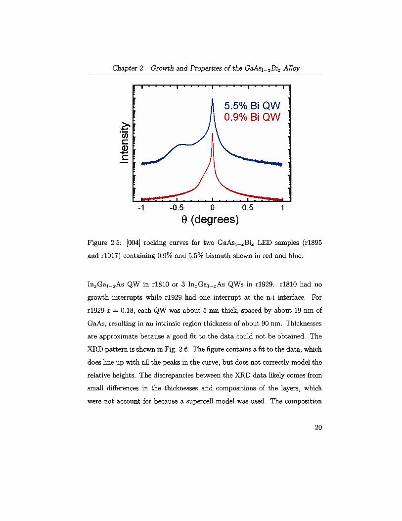
layer is 890 nm. Two other GaAsi_Bi n-i-p structures, one containing
about 0.9% Bi and the other 5.5% Bi are shown in Fig. 2.5. Table 2.1
summarizes all the LED structures that were grown.
Cl)CU)C
Figure 2.4: [004] rocking curve of a GaAsi_Bi LED sample (r1965) con
taining 1.8% bismuth. A fit to the data is shown in red
InGai_As LEDs were grown for comparison with the GaAsi_Bi LEDs.
The n-type and p-type layers of these devices were similar to the struc
ture discussed above, however the intrinsic region contained either a single
-1000 0 1000
9 (seconds)
19
Chapter 2. Growth and Properties of the GaAs1_Bi Alloy
>
Cl)C
C
Figure 2.5: [004] rocking curves for two GaAsi_Bi LED samples (r1895
and r1917) containing 0.9% and 5.5% bismuth shown in red and blue.
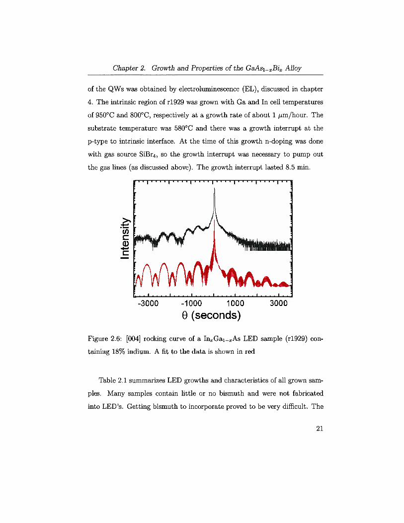
InGai_As QW in r1810 or 3 InGai_As QWs in r1929. r1810 had no
growth interrupts while r1929 had one interrupt at the n-i interface. For
r1929 x = 0.18, each QW was about 5 nm thick, spaced by about 19 nm of
GaAs, resulting in an intrinsic region thickness of about 90 urn. Thicknesses
are approximate because a good fit to the data could not be obtained. The
XRD pattern is shown in Fig. 2.6. The figure contains a fit to the data, which
does line up with all the peaks in the curve, but does not correctly model the
relative heights. The discrepancies between the XRD data likely comes from
small differences in the thicknesses and compositions of the layers, which
were not account for because a supercell model was used. The composition
-1 -0.5 0 0.5
9 (degrees)
20
Chapter 2. Growth and Properties of the GaAsi_Bi Alloy
of the QWs was obtained by electroluminescence (EL), discussed in chapter
4. The intrinsic region of r1929 was grown with Ga and In cell temperatures
of 950°C and 800°C, respectively at a growth rate of about 1 pm/hour. The
substrate temperature was 580°C and there was a growth interrupt at the
p-type to intrinsic interface. At the time of this growth n-doping was done
with gas source SiBr4, so the growth interrupt was necessary to pump out
the gas lines (as discussed above). The growth interrupt lasted 8.5 mm.
Cl)Cci)C
Figure 2.6: [004] rocking curve of a InGai_As LED
taming 18% indium. A fit to the data is shown in red
sample (r1929) con-
Table 2.1 summarizes LED growths and characteristics of all grown sam
ples. Many samples contain little or no bismuth and were not fabricated
into LED’s. Getting bismuth to incorporate proved to be very difficult. The
-3000 -1000 1000 3000
0 (seconds)
21

Chapter 2. Growth and Properties of the GaAs1_Bi Alloy
conditions for bismuth incorporation are very precise and perhaps if detailed
calibrations of fluxes were done before each growth then more reproducible
compositions of GaAsi_Bi layers would have been obtained. Table 2.2
gives more detailed growth information from the most significant samples.
Beam equivalent pressures (BEPs) are given as read from ion gauge and
are based on flux calibrations done weeks or even months before the ac
tual growths. BEPs have not been corrected for the sensitivities of different
chemical species.
22

Tab
le2.
1:S
umm
ary
ofal
llig
htem
itti
ngdi
ode
sam
ples
grow
n,in
clud
ing
faile
dat
tem
pts.
Sam
ple
Gro
wth
Bi
orIn
EL
Wav
elen
gth
Com
men
ts
Log
#In
terr
upts
{%]
(nm
)
r181
00
In[3
.6]
med
ium
900
very
resi
stiv
e
r185
20
In[01
NA
NA
did
not
rect
ify
r187
50
In[2
1jN
AN
Ave
ryle
akey
,ov
erdo
ped
p-la
yer
r188
81
Bi[0
.5]
NA
NA
not
test
ed,
wan
ted
mor
eB
i
r189
51
Bi[0
.9]
Non
eN
Aon
lyde
fect
emis
sion
r190
11
Bi[0
]N
AN
Ano
tte
sted
,no
Bi
r191
72
Bi[5
.5]
Ver
yw
eak
1300
mos
tly
defe
ctem
issi
onan
dG
aAs
r192
91
Inx3
[18]
Str
ong
1025
very
stro
ngE
L,
good
IV
r193
02
Bi[
NA
]N
AN
Adr
oppe
din
MB
E-p
ost
grow
th
r196
21
Bi[
NA
]N
AN
Aco
vere
din
Ga
duri
nggr
owth
r196
51
Bi[1
.8]
Str
ong
986
see
text
r197
00
Bi[0
]N
AN
Ano
tye
tte
sted
r198
21
GaA
sN
AN
Ahi
ghT
GaA
sno
tye
tte
sted
r198
50
Bi[0
]N
AN
Ano
tye
tte
sted
0 0 € 0 Cb
03

Chapter 2. Growth and Properties of the GaAsi_Bi Alloy
Table 2.2: Summary of growth conditions of significant samples.
Sample Substrate P[Ga] P[Asj P[In or Bi]
Log # Temp. (°C) (torr) (torr) (torr)
r1895 315 3.0 x iO 2.9 x 1O [Bi]3 x 1O
r1917 305 1.8 x iO 1.6 x 1O [Bi]6 x iO
r1929 580 9.4 x 1O 4.9 x 10—6 [In]3 x 1O
r1965 310 0.8 x iO 0.7 x iO [Bi]7 X 10
24

Chapter 3
Post-Growth Fabrication of
Light Emitting Diodes
3.1 Ohmic Contacts
One challenge faced in post-growth fabrication of semiconductor electrical
devices is making reliable ohmic contacts. An ohmic contact is an electrical
contact, which has a linear I-V responce curve, and ideally should have the
lowest series resistance possible. Contacts should be easily reproducible and
stable over the usable temperature range of the device. This seemingly simple
task has been the focus of an enormous amount of research over the past
several decades. For more information and selected review articles on ohmic
contacts Modern GaAs Processing Methods by Williams [23] contains much
useful information, also see the review article by Shen[24]
Normally, when a metal is put in intimate contact with a semiconductor,
a depletion region forms in the semiconductor, which bends the bands so
that the Fermi level is equal in the metal and the semiconductor. One would
expect that the voltage across the barrier (q5) would simply be the difference
in the work function of the metal @m) and the electron affinity (x) for the
case of an n-type semiconductor as shown in Eq. 3.1. In the case of a p-type
25

Chapter 3. Post-Growth Fabrication of Light Emitting Diodes
semiconductor, it would be expected that the barrier voltage would be the
difference between the and the sum of x and the bandgap energy (Eg),
as shown in Eq. 3.2 and illustrated in Fig. 3.1. Fig. 3.1 shows a schematic
of band bending for an ideal metal to n-type semiconductor interface as
described above.
b—n type = — X (3.1)
b-ptype =qm—(X+Eg) (3.2)
Based on this reasoning, by choosing metals with different work functions
it should be possible to achieve a large range of values for A metal-
semiconductor combination where cbb = 0 should result in an ohmic contact,
based on this logic. In practice, most metals have the same barrier height of
about 0.8 V when put in contact with n-doped GaAs, even though the above
discussion would predict that barrier heights from 0.07 V to 0.57 V should
be possible [23]. The reason is that the surface states of the semiconductor
actually set the barrier height. Fig. 3.2 shows a schematic of a more realistic
metal to n-type semiconductor interface.
Current can flow across the metal-semiconductor interface by either thermionic
emission, or quantum mechanical tunneling through the barrier, which can
be enhanced by applying a large electric field (field emission). Thermionic
emission is the main mechanism for current flow through a Shottky diode,
while current flow through ohmic contacts is usually due to tunneling. The
current density for field emission through a barrier of height q has the form
of Eq. 3.3, where e is the magnitude of the electron charge and E00 is given
26

Chapter 3. Post-Growth Fabrication of Light Emitting Diodes
Figure 3.1: Schematic diagram of a metal to n-type semiconductor interface
in the absence of surface states.
in Eq. 3.4. Here 7. is Plancks constant, N is the doping concentration, c is
the dielectric constant and m* is the effective mass[25j. It is worth noting
that as the doping is increased the tunneling current increases exponentially.
This is attributed to narrowing of the depletion region/barrier.
J c expE00 (3.3)
where
E00 = (3.4)
To make a good ohmic contact it’s necessary for the surface layer to
be highly doped (usually in the 1019cm3 range for n-type and 1020cm3)
range for p-type[23]. To achieve this high level of doping the contact ma-
Ips
27

Chapter 3. Post-Growth Fabrication of Light Emitting Diodes
1EE
ESurface States
Figure 3.2: Schematic diagram of a metal to n-type semiconductor interface
with surface states.
terial usually contains an element, which will diffuse upon annealing into
the semiconductor, producing a highly doped surface layer. In the case of
AuGe n-contacts, which were used for n-type contacts here, this element
is germanium[23]. For contacting n-type GaAs, AuGe-based contacts have
been the most successful, even though they are somewhat inconsistent and
the resistivity depends strongly on how well optimized the annealing condi
tions are. Typical contact resistivities of AuGe-based contacts range from
0.8 x 10—6 cm2 to 4 x 10—6 cm2[23].
Another method for improving ohmic contacts is to grade the composition
of the surface layer by alloying, into a low bandgap semiconductor, such as
InAs. This method is not widely used for GaAs as many complications, such
as lattice matching arise[23].
Many different material combinations are used to make ohmic contacts to
GaAs. For contacting the p-doped side of our LED’s Ti/Pt/Au contacts were
28

Chapter 3. Post-Growth Fabrication of Light Emitting Diodes
used [26] [27]. These contacts were selected because of their stability over a
the wide annealing range of 420 C to 530 C and extremely low demonstrated
contact resistance of 2.8 x 10—8 flcm2[26]. Small circular Ti/Pt/Au p-type
ohmic contacts with a diameter of 0.32 mm were deposited through a metal
shadow mask using e-beam evaporation. Ti/Pt/Au thicknesses of about
50 nm/100 nm/200 nm were used. Each circular p-type contact defined a
single device on top of the wafer. n-type contacts were made by evaporation
of Ni/AuGe/Au [23] [28] onto the entire back side of the sample, forming
a common contact with all the top contacts on the sample. Ni/AuGe/Au
thicknesses of about 25 nm/100 nm/200 nm were used. Proper annealing
temperatures for the n-type contact on the back were ignored because of the
large surface of the contact. After deposition, the wafer was annealed at
450°C for 20 seconds after deposition to improve the contact conductivity.
The resistivity of Ti/Pt/Au contacts was tested by depositing a line of
the 0.32 mm diameter metal dots onto an p-doped (about 2 x 1018 cm3)
GaAs wafer cleaved to be about 1 mm by 25 mm. Contact resistances of
about one ohm were found by measuring the resistance between dots as
a function of separation distance, corresponding to a specific resistivity of
about 5 x iO lcm2. It is expected that much lower contact resistivities
could be obtained if higher doping concentrations were used, but these values
were deemed adequate for test LEDs. Current voltage curves were confirmed
to be linear over the current range of interest and dot-to-dot uniformity was
excellent.
29
Chapter 3. Post-Growth Fabrication of Light Emitting Diodes
3.2 Mesa Etching
After contacts were deposited and annealed, the top 300 nm of highly doped
GaAs around the contacts was etched off using aH2S04:H202:H20wet etch
with volume ratios of 4:1:5 [23], which removed 5tm/min for a room tem
perature solution. The highly doped top layer was removed to minimize
current spreading. This etch was selected because it did not seem to dam
age the Ti/Pt/Au contacts, while some other etches removed the metal all
together. The depth of the etch was measured with profilometry. It was dis
covered that etching through the intrinsic region resulted in high leakage and
no light emission, attributed to non-radiative surface recombination. After
mesas were etched, the sample was cleaved into sizes of about 5 mm by 3 mm
and bonded to a small piece of copper using silver epoxy. Contact was made
to the dots by wire bonding the dots to terminals, which were glued to the
copper piece. Fig. 3.3 shows a schematic of the LED chip after metalization
and etching. The dashed lines indicate possible growth interrupts (depend
ing on the sample). Most early samples were not etched, resulting in poor
current-voltage characteristics.
30

Chapter 3. Post-Growth Fabrication of Light Emitting Diodes
Figure 3.3: Schematic of an LED chip after metalization and etching. Typical
thickness for i-GaAs layers was 25 nm, typical GaAsBi QW thicknesses were
30 nm to 50 urn and typical p-GaAs thickness was 1 /mum. The top 300 nm
of the p-GaAs layer was removed by etching.
n-contact (Ni/AuGe/Au)
31

Chapter 4
Electrical Characterization
4.1 Current-Voltage Measurements of
GaAsi_Bi Diodes
Current-Voltage (I-V) measurements were made with a Keithley 220 current
source and a Keithley 197A voltmeter, using a 2-probe method. According
to Keithley specification sheets the current source had an output resistance
greater than 1014 Q, absolute accuracy of sourced currents less than 0.1%
over the current ranges used and 100 ppm noise in the source. The voltmeter
had a resistance greater than 1 GQ in the 2 V range and a resolution of
10 jtV. Both the current source and voltmeter were interfaced to a computer
through an IEEE 488 interface, and controlled using an in-house-made Lab-
View program. I-V measurements were made over the current ranges from
10 [LA reverse bias to 10 mA forward bias, usually with 10 data points taken
per decade and a minimum step size of 100 nA. Unless otherwise mentioned,
I-V measurements were made at room temperature.
Fig. 4.1 shows current-voltage measurements of several devices from sam
ple r1965, containing 1.8% bismuth. r1965 was the only GaAsi_Bi LED
to show strong electroluminescence and it thus highlighted here. Dot to dot
uniformity was excellent, as the curves have excellent overlap.
32

Chapter 4. Electrical Characterization
1x10² .:‘:::‘:::;‘:
1x10
1x10
lxi 0 1
lxlfY6
1x10⁷I • •I_ • • I • • I
-1.5 -1 -0.5 0 0.5 1 1.5Potential (V)
Figure 4.1: Current-Voltage curves for four GaAs1_Bi light emitting diodes
at 300 K. The red line indicates a fit to the data with n = 2.26 ideality factor.
33

Chapter 4. Electrical Characterization
The leakage current was approximately 5 tA at a reverse bias of 1 V.
Fitting the forward bias data over the current range i0 A to iO A to the
diode equation gives a saturation current (Is) of 7.1 A/cm2with a standard
deviation of 0.4 1A between dots. The fit also gave ideality factor of 2.26.
Series resistances of 100 Q with standard deviation of less than 10 were
measured at high currents. The reason for the high series resistance is un
known. The resistance is believed not to be due to the ohmic contacts, as
contact resistance is expected to be less than 1 Q as inferred from measure
ments on the p-doped wafer, which had similar doping concentrations.
Fig. 4.2 shows current voltage data for another GaAsi_Bi sample (r1895),
which was found to emit some light. The hollow data points with low reverse
bias leakage current are from different diodes for a device prepared soon after
growth, where no etching was done to remove the top highly doped GaAs
layer. The sample was remeasured after about 2 months (red solid circles)
and reverse bias leakage was an order of magnitude greater. The sample was
then dipped in HC1 to remove any oxide that may have formed and remea
sured (black solid diamonds), where it showed the same level of high leakage.
A second sample was fabricated from growth r1985, where the top highly
doped GaAs layer was removed, but still showed the high leakage (pink solid
triangles) observed before. This very unusual degradation has no obvious
explanation.
34

Chapter 4. Electrical Characterization
1x10² • • I
1x10³
1x10⁴
•......D 1x10⁵ \
C.)
•‘••.
Potential (V)
Figure 4.2: Current-Voltage curves for GaAsi_Bi LED r1895. Hollow data
points (low leakage values on reverse bias) correspond to dots from an un
etched device fabricated soon after growth. Solid data points (high leakage)
correspond to measurements made on the same sample 2 months later, with
and without dipping the sample in HC1 to remove possible oxide and also
for a new device fabricated from the wafer with etched mesas (solid pink
triangles).
35

Chapter 4. Electrical Characterization
4.2 Current-Voltage Measurements of
InGai_As Diodes
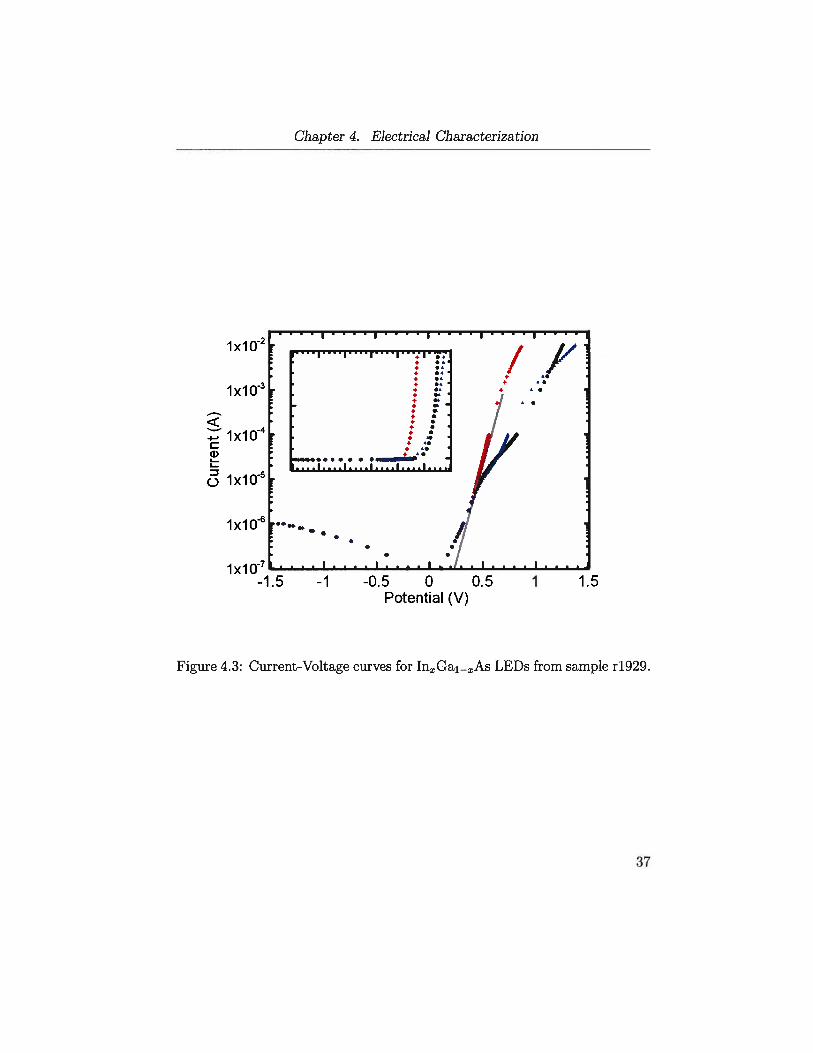
Fig. 4.3 shows I-V curves for three 1n0,18Ga082As diodes fabricated from
sample r1929 at the same time. The top highly doped layer of GaAs was
removed by etching. The leakage current at —1 V was observed to be about
0.5 ILA (an order of magnitude less than for the GaAsi_Bi sample r1965).
Dot to dot uniformity was very good on reverse bias and for forward bias
for voltages less than 0.4 V. At higher voltages the diodes behaved very
inconsistently. Only the red curve in Fig. 4.3 showed the expected “rolling
over” on the semilog plot due to the series resistance dominating the I-V
shape, the red and black curves appeared to roll over at 0.5 V, but then
curved back up before rolling over again. One possible explanation for this
is that irreversible changes were taking place in these samples causing the
devices to fail. The diodes were only tested once so this explanation has not
been confirmed. All the diodes were observed to be strong light emitters.
36
Chapter 4. Electrical Characterization
lxi 02
lxi Q..3
Z ixiO4C
1
-5o ixi0
lxi .6
lxi-1.5 -1 -0.5 0 0.5
Potential (V)1 1.5
Figure 4.3: Current-Voltage curves for InGa1_As LEDs from sample r1929.
37
I I
I
,. ..+ .+ .• .a+ .‘+ .&
+ .+ .+ a
+ a+ a• .
+ •+ .• .• ‘•+ ‘.
+ .+ ‘.
•4a...... . . ..
.1. .. .1. • •.I.. • .1. •. .1. •.
a.•
• • • • I • .
/ .1
.
.1

Chapter 5
Optical Characterization
5.1 Electroluminescence (EL) and
Photoluminescence (PL)
Luminescence is the emission of photons of light when an atom, molecule, or
crystal system decays from an excited state to a lower energy state. Types
of luminescence are classified by the method of excitation. Here we discuss
electroluminescence (EL), which is the emission of photons, by a material
in responce to an applied voltage. We also discuss Photoluminescence (PL),
which is the absorption and then re-emission of photons by a material.
Electrons can transition from an occupied initial state to a vacant final
state, where the occupation probability of an energy state is given by the
value of the Fermi function. The absorption and stimulated emission rates
R12 and J-?21 and the spontaneous emission rate R8 thus can be written in
the form in Eq.5.1, where R, and R0 are the transition rates of stimulated
and spontaneous processes if all state pairs are available. f and f are the
Fermi functions for the valence and conduction bands. Using Einsteins coef
ficients A and B as rate constants for spontaneous and stimulated processes
respectively R0 = A and R,. = BW(zi), where W(v) is the radiation spectral
density [20].
38

Chapter 5. Optical Characterization
R12 = Rrfv(l fc) (5.1)
R21=Rrfc(lfv) (5.2)
R3 = R0f(1— f) (5.3)
In the case of PL in semiconductors, light with energy greater than the
bandgap is incident on the semiconductor. Electrons in the valence band
absorb photons and are excited to the conduction band, creating electron hole
pairs, which can recombine either radiatively, or by a non-radiative process.
The main types of non-radiative recombination processes in semiconductors
are defect, surface and auger recombination, these are briefly discussed at
the end of this section. Photoluminescence measurements give information
about the electronic properties, such as material bandgap. The high energy
side of the emission spectum is attributed to thermal excitation of electrons
to higher energy levels in the conduction band, and similarly for holes in
the valence band. The shape of this tail can be modeled by a Boltzmann
distribution for relatively high temperatures (T > 100 K), as indicated in
Eq. 5.4, where Ih(E) is the intensity at photon energy E, k is the Boltzmann
constant and T is the absolute temperature.
Ih(E) = Ae (5.4)
Emission below the gap is possible due to thermal fluctuations in the
lattice, and structural inhomogeneities. This low energy side of the peak
can be modeled using the product of an Urbach edge [29] and a Boltzmann
distribution, as shown in Eq. 5.5, where 11(E) is the intensity at photon
39

Chapter 5. Optical Characterization
energy E, c is the 0 K absorption coefficient at the bandgap energy E9 and
E0 is the Urbach parameter.
E-E9 -
f(E) = ge Eo e kT (5.5)
Light emission from LEDs is primarily a spontaneous emission process.
From Eq. 5.1 we see that the rate of spontaneous emission between two
levels is proportional to the product of the probability that the upper state
is occupied and the probability the lower state is vacant. When a voltage
is applied across an LED it causes a separation of quasi-Fermi levels equal
to the applied voltage, which causes the occupation of a given level in the
conduction band to increase and a decrease of the occupation of energy levels
in the valence band, thus increasing the spontaneous emission rate.
Non-radiative recombination can be a significant, or even the dominant
form of loss in a device depending on material quality and device design.
There are three main types of non-radiative recombination; defect, surface
and Auger recombination as shown in Fig. 5.1. Defect recombination is due
to impurity atoms or defects in the crystal, which have mid-gap energy levels.
In this case the electron can fall from the conduction band to the defect level
and then recombine with a hole, thus depleting the conduction band without
producing photons. Surface recombination is similar to defect recombination,
except the mid-gap levels are surface states. Auger recombination requires
two electrons in the conduction band. One electron falls to the valence band
but the energy is used to push the other electron up to a higher energy level,
thus depleting the conduction band without producing light.
40

Chapter 5. Optical Characterization
__zN
_
• • Ev
Surface Auger
Figure 5.1: Possible non-radiative transitions in semiconductors.
5.2 Photoluminescence Measurements
As a semiconductor is cooled, it is expected that the bandgap will shift
to higher energy. The shift in bandgap comes from a combination of a
temperature-dependant dilation of the lattice and a temperature depen
dent electron-lattice interaction[30J. The temperature dependence can be
described by the Varshni equation shown in 5.6, where a and /3 are con
stants, Eg is the bandgap energy at absolute temperature T and E0 is the
bandgap energy at T = 0 K. For GaAs, a = 8.871x10⁴eV/K, /3 = 572 K
and E0 = 1.5216eV[31].
aT2E9(T) = E0-I-
/3+T(5.6)
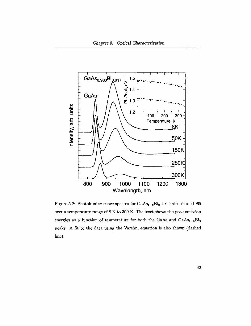
Fig. 5.2 shows photoluminescence spectra for a series of temperatures
from 8 K to room temperature (300 K) for GaAs1_Bi sample r1965. The
532 nm green pump laser and collecting optics were focused on the area be-
Defect
41
Chapter 5. Optical Characterization
U).1
>
U)
a)
1200 1300
Figure 5.2: Photoluminescence spectra for GaAs1_Bi LED structure r1965
over a temperature range of 8 K to 300 K. The inset shows the peak emission
energies as a function of temperature for both the GaAs and GaAs1_Bi
peaks. A fit to the data using the Varshni equation is also shown (dashed
line).
800 900 1000 1100Wavelength, nm
42

Chapter 5. Optical Characterization
tween the metal dot contacts on the top of the sample. A clear peak was
observed for both GaAs (870 nm) and GaAsi_Bi (975 nm), along with
a wide low energy tail which is attributed to shallow defect states in the
bandgap. The GaAsi_Bi peak emission wavelength at room temperature
agrees with the expected shift in bandgap energy for 1.8 % bismuth incor
poration, 0.16 eV[6]; this estimate for the bismuth content is consistent with
a fit to the split off peak seen in the [0041 XRD rocking curve which gave
x = 1.7 ± 0.2% for GaAsi_Bi. Both the GaAs and GaAsi_Bi peaks
blue shifted with decreasing temperature (inset of Fig. 5.2) and followed the
Varshni equation[30]:
In the fit in the inset of Fig. 5.2, E0 for GaAs is 1.48 eV and E0 = 1.32 eV
for GaAs0982Bi0,018,with = 0.36 meV/K and /3 = 356 K in equation 5.6 for
both fits. The change in E0 corresponds to 1.8% bismuth, based on 88 meV
band gap reduction per percent bismuth incorporation[6]. Temperature de
pendent PL measurements were not made on other samples.
5.3 Electroluminescence Measurements
Electroluminescence (EL) measurements were made at room temperature
unless otherwise stated. The light was collected from the periphery of the
top metal dot, since the metal dot was opaque. EL spectra from GaAsi_Bi
light emitting diode r1965 are shown in Fig. 5.3 for forward bias current
densities of 50 A/cm2, 75 A/cm2 and 100 A/cm2.
Two clear peaks are seen: GaAs at 870 nm and GaAsi_Bi at 987 nm,
along with a low energy tail. With increasing current density a slight blue
43

Chapter 5. Optical Characterization
Cl)
CD
>
Cl)Cci)
-I-.C
Figure 5.3: Electroluminescence spectra for a GaAsi_Bi light emitting
diode from sample r1965 for various injection current densities at 300 K.
Room temperature photoluminescence is shown for comparison.
800 900 1000 1100 1200Wavelength, nm
44

Chapter 5. Optical Characterization
shift in the peak emission wavelength of the GaAsi_Bi band to band peak
was observed, attributed to a further separation of quasi-Fermi levels at
higher pumping currents. The shape of the spectra did not change. The
GaAsi_Bi peak intensity was found to be superlinear with increasing cur
rent density, possibly due to defect recombination saturation, resulting in a
higher fraction of additional carriers recombining radiatively.
The room temperature PL is also shown in Fig. 5.3 for comparison. PL
peaks are blue shifted relative to the EL peaks and the low energy emission
from the defect states is much stronger in the EL spectra. Both of these ob
servations can be explained by the differences in the way carriers are injected
for PL and EL. In the former case carriers are injected with energies larger
than the bandgap, while in the latter case electrically injected carriers have
energies close to the band edges and are thus restricted to low energy states.
This results in an increasing tendency for recombination from higher energy
states to occur in the case of PL.
Earlier LED samples performed more poorly than r1965 LEDs. Fig. 5.4
shows EL spectra from three GaAsi_Bi LEDs at 100 A/cm2 injection cur
rent. The black and red data are from two diodes (fabricated separately)
from sample r1895, which contained about 1% bismuth. The blue data is
from r1917, which contained 5.5% bismuth. EL intensity was very weak,
compared to sample r1965 discussed above. All spectra show a peak at
870 nm, corresponding to GaAs and broadband emission at wavelengths ex
ceeding 1000 nm, corresponding to emission from defects. Long wavelength
emission intensities in Fig. 5.4, whether from defects or the GaAsi_Bi
layer, are all more than an order of magnitude smaller than the emission
45

Chapter 5. Optical Characterization
from the GaAsi_Bi layer from sample r1965 at the same injection cur
rent. The long wavelength emission from r1895 could not have come from
the GaAsi_Bi layer since XRD measurements from Fig. 2.5 showed the
GaAsi_Bi layer had x = 0.01. Based on 88 meV reduction of the bandgap
per percent bismuth{6], the GaAsi_Bi peak should have been at 930 nm.
Sample r1917 was found by XRD measurements to have x = 0.055 in the
GaAsi_Bi, which would put the expected GaAsi_Bi peak at 1325 nm.
Looking at the EL spectra in Fig. 5.4 it appears that the long wavelength
emission (1000 nm to 1300 nm) from r1917 is composed of two broad peaks,
the longer of which is at about 1300 nm, hence it is possible that some of this
emission came from the GaAsi_Bi layer. r1917 also had two growth inter
rupts, which is expected to have increased the amount of defects resulting in
further loss in the EL from the GaAsi_Bi layer.
Fig. 5.5 shows EL from the InGai_As LED (1929) with x=0.18 for
current densities of 12 A/cm2, 25 A/cm2, 37 A/cm2 and 62 A/cm2. The
spectra show a small GaAs peak at 870 nm and a large peak at 1025 nm from
the InGai_As QWs. As observed with the GaAsi_Bi LED, the peak of
the InGai_As emission slightly blue shifted with increasing current density,
due to further separation of the quasi-Fermi levels. No long wavelength tail
from defects was observed in this sample. Unlike the GaAsi_Bi LED, which
showed super-linear light emission, emission form the InGai_As device was
sub-linear, as can be seen in Fig. 5.5. This suggests that there was less non
radiative defect recombination to saturate. The integrated room temperature
intensity of the InGa1_As device was about 100 x higher than for the r1965
GaAsi_Bi device at the same current. Quantum wells are known to be
46

Chapter 5. Optical Characterization
C,)
CD
-Q(‘3
>
C’)
G)C
Figure 5.4: Room temperature electroluminescence spectra from three
GaAsi_Bi LEDs at 100 A/cm2 injection current. The black and red spec
tra were fabricated from growth r1895 and contain 1% bismuth. The blue
spectra (from r1917) contained 5.5% bismuth in the GaAsi_Bi layer.
800 1000 1200Wavelength, nm
47

Chapter 5. Optical Characterization
D
Cl)
C
1100
Figure 5.5: Room temperature electroluminescence spectra for an
InGa1_As light emitting diode for various injection current densities.
900 1000Wavelength, nm
48

Chapter 5. Optical Characterization
more efficient than bulk layers and it is expected that had the GaAsi_Bi
device also contained 3 similarly sized quantum wells that it would have been
brighter than the existing GaAsi_Bi design.
5.4 Temperature Dependent
Electroluminescence
Fig. 5.6 shows the temperature dependence of the r1965 GaAs1_Bi LED
EL spectra at 50 A/cm2 from 100 K to 300 K.
As the temperature decreased, a clear blue shift in the peak wavelength
of the GaAs in agreement with PL results was observed. Both the emission
from the GaAs1_Bi peak and the longer wavelength shallow defect states
increased with decreasing temperature. However, emission from the defect
states also increased relative to the GaAs1_Bi band to band peak. At 100 K
the intensity of defect emission surpassed the emission of the GaAsi_Bi
band to band peak. In contrast to the PL measurements shown in Fig. 5.2,
the intensity of the GaAs peak decreased as the device was cooled. This re
sulted from a greater carrier confinement in the smaller bandgap GaAs1_Bi
layer. No shift in peak wavelength of the GaAsi_Bi emission was observed
over this temperature range. This can be explained by two competing pro
cesses, the increase in the bandgap at lower temperature and the increased
tendency for emission to come from lower energy states at lower tempera
tures. These two processes combined result in the observed temperature in
dependent peak emission wavelength of the GaAsi_Bi band to band elec
troluminescence. The temperature sensitivity of PL measurements can be
49

Chapter 5. Optical Characterization
(I)
CD
>
U)Ca)C
Figure 5.6: Electroluminescence spectra from GaAsBi LED r1965 at
50 A/cm2 injection current density for temperatures ranging from 100 K
to 300 K.
800 900 1000 1100 1200Wavelength, nm
50

Chapter 5. Optical Characterization
explained by the low density of states of the GaAsi_Bi impurity like states
in the bandgap. It is possible that as the temperature is lowered PL emission
of these lower energy states does not increase because the electrons-hole pairs
recombine before they have a chance to find the deeper impurity-like states.
51

Chapter 6
Conclusion
GaAsi_Bi is an exciting new semiconductor with promising applications
as a new infrared light source. The characteristics of the GaAsi_Bi appear
to be well matched to the requirements for optical coherence tomography.
We have developed a method for the growth and fabrication of GaAsi_Bi
light emitting diodes, based on a simple n-i-p structure containing one GaAsi_Bi
layer in the intrinsic region. n-i-p structures with up to 5.5% bismuth in the
GaAsi_Bi layer have been realized. Strong light emission was obtained
from a sample containing 1.8% bismuth with emission centered at 987 nm.
This GaAs1_Bi emission peak was found to be independent of temperature
over the temperature range 100 K to 300 K. The long wavelength emission
did increase, which changed the shape of the spectra.
The temperature insensitivity of the GaAsi_Bi electroluminescence can
be explained by two competing processes; the increase in the bandgap with
decreasing temperature and the tendency for emission to come from lower
energy states as temperature is decreased. Photoluminescence measurements
on the same device showed a temperature dependence of the GaAsi_Bi
band to band transition consistent with measurements by Francoeur [6]. Both
the electroluminescence and photoluminescence spectra have large spectral
widths which is a reflection of the impurity-like nature of the states associated
52

Chapter 6. Conclusion
with bismuth incorporation. Difficulties incorporating bismuth into the n-i-p
structure are an unresolved issue as well as the poor performance of many of
the GaAsi_Bi layers.
This demonstration of a GaAsi_Bi based LED opens up a new class of
materials for long wavelength semiconductor light sources with broad emis
sion spectra.
6.1 Future Work
Much work must still be done to reliably grow GaAsi_Bi LED structures
with the desired amount of bismuth. The fact that many of the growths did
not show strong luminescence from the GaAs1_Bi layer also requires further
investigation. GaAs n-i-p samples grown at different growth conditions were
grown but have not yet been fabricated and characterized, this will have to
be done to investigate whether the low temperature GaAs or the GaAsi_Bi
layer is the source of the impurity emission. New GaAs1Bidevices should
also be grown and fabricated in attempt to obtain strong electroluminescence
from a GaAsi_Bi light emitting diode with 1.0 eV bandgap. This will show
that GaAsi_Bi devices can exceed the wavelength range of InGai_As
devices. Improvements to this rudimentary test device could be made by:
optimizing the thicknesses of the GaAsi_Bi and undoped GaAs layers; op
timizing contact design; the use of an A1GaAs double heterostructure design;
and removing the growth interrupt.
53

Bibliography
[1] H. Foil. Christian-Albrechts-University of Kiel, http://www.tf.uni
kiel.de/matwis/amat/semLen/kap5/backbone/r5_1_4.html.
[2] X. Lu, D. Beaton, T. Tiedje, R. Lewis, M.B. Whitwick. Effect of MBE
Growth Conditions on Bi Content of GaAsi_Bi. Applied Physics Let
ters, 92, 2008.
[3] M.J. Antoneli, C.R. Abernathy, A. Sher, M. Berding, M. Van Schiif
gaarde, A. Sanjuro K. Wong. Growth of Ti-Containing ITT-V Materials
by Gas-Source Molecular Beam Epitaxy. Journal of Crystal Growth,
188:113—118, 1998.
[4] S. Tixier, M. Adamcyk, E.C. Young, J.H. Schmid, T. Tiedje. Surfactant
enhanced growth of GaNAs and InGaNAs using bismuth. Journal of
Crystal Growth, 251:449—454, 2003.
[5] K. Oe, H. Okamoto. New Semiconductor Alloy GaAsi_Bi Grown
by Metal Organic Vapor Phase Epitaxy. Japanese Journal of Applied
Physics Part 2, 37:L1283—L1285, 1998.
[6] J. Yoshida, T. Kita, 0. Wada, K. Oe. Temperature Dependence
of GaAsl-xBix Band Gap Studied by Photoreflectance Spectroscopy.
Japanese Journal of Applied Physics Part 1, 42:371, 2003.
54

Bibliography
[7] S. Francoeur, M.J. Seong, A. Mascarenhas, Sebastien Tixier, Martin
Adamcyk, Thomas Tiedje. Band Gap of GaAsi_Bi, 0<3.6%. Applied
Physics Letters, 82:3874—3876, 2003.
[8] S. Adachi. Physical Properties of 111-V Semiconductor Compounds. Wi
ley, 1992.
[9] T. Tiedje, E.C. Young, A. Mascarenhas. Growth and Properties of the
Dilute Bismide Semiconductor GaAsi_Bi a Complementary Alloy to
the Dilute Nitrides. International Journal of Nanotechnology, 5:963—983,
2008.
[10] l.A. Janotti, S.H. Wei, S.B. Zhang. Theoretical study of the effects of
isovalent coalloying of Bi and N in GaAs. Physical Review B, 65:115203,
2002.
[11] 1.W. Shan, W. Walukiewicz, J.W. Ager, E.E. Haller, J.F. Geisz, D.J.
Friedman, J.M. Olson, S.R. Kurtz. Band Anticrossing in GaInNAs Al
loys. Physical Review Letters, 82:1221, 1999.
[12] A. Mascarenhas, Y. Zhang, J. Veerley, M.J. Seong. Overcoming Limita
tions in Semiconductor Alloy Design. Superlattices and Microstructures,
29:395, 2001.
[13] L. Vegard. Die Konstitution der Mischkristalle und die Raumfullung der
Atome. Z. Physik, 5:17, 1921.
[14] U. Tisch, E. Finkman, J. Salzman. The anomalous bandgap bowing in
GaAsN. Applied Physics Letters, 81:463—465, 2002.
55

Bibliography
[15] E. Nodwell, M. Adamcyk, A. Ballestad, T. Tiedje, S. Tixier, S.E. Web
ster, E.C. Young, A. Moewes, E.Z. Kurmaev, T. van Buuren. Tight-
Binding Model for the X-ray Absorption and Emission Spectra of Dilute
GaNxAsl-x at the Nitrogen K edge. Physical Review B, 69:15520, 2004.
[16] K. Oe. Characteristics of Semiconductor Siloy GaAsl-xBix. Japanese
Journal of Applied Physics Part 1, 41:2801—2806, 2002.
[17] D. Huang, E.A. Swanson, C.P. Lin, J.S Schuman, W.G. Stinson, W.
Chang, M.R. Hee, T. Flotte, K. Gregory, C.A. Puliafito, J.G. Fujimoto.
Optical Coherence Tomography. Science, 254:1178—1181, 1991.
[18] J.M. Schmitt. Optical Coherence Tomography (OCT): A Review. IEEE
Selected Topics in Quantum Electronics, 5:1205, 1999.
[19] M.R. Pillai, S.S Kim, S.T. Ho, S.A. Barnett. Growth of
InGaiAs/GaAs heterostructures using Bi as a surfactant. Journal
of Vacuum Science and Technology B, 18:1232—1236, 2000.
[20] E.C. Young, S. Tixier, T. Tiedje. Bismuth Surfactant Growth of the
Dilute Nitride GaNAsi_. Journal of Crystal Growth, 279:316—320,
2005.
[21] L.A. Coidren, S.W. Corzine. Diode Lasers and Photonic Integrated Cir
cuits. Wiley Series in Microwave and Optical Engineering, 1995.
[22] M. Balkanski, R.F. Wallis. Semiconductor Physics and Applications.
Oxford, 2000.
56

Bibliography
[23] S.R. Johnson, C. Lavoie, T.Tiedje. Semiconductor Substrate Temper
ature Measurement by Diffuse Reflectance Spectroscopy in Molecular
Beam Epitaxy. Journal of Vacuum Science and Technology B, 11:1007—
1010, May 1993.
[24] R. Williams. Modern GaAs Processing Methods. Artech House, 1990.
[25] T.C. Shen, GB. Gao, H. Morkoc. Recent Developments in Ohmic Con
tacts for ITT-V Compound Semiconductors. Journal of Vacuum Science
and Technology B, 10:2113—2132, 1992.
[26] S.M. Sze. Physics of Semiconductor Devices. John Wiley and Sons,
1981.
[27] G. Stareev. Formation of Extremely Low Resistance Ti/Pt/Au Ohmic
Contacts to p-GaAs. Applied Physics Letters, 62:2801—2803, 1993.
[28] A. Katz, C.R. Abernathy, S.J. Pearton. Pt/Au Homic Contacts to Ul
trahigh Carbon-doped p-GaAs Formed by Rapid Thermal Processing.
Applied Physics Letters, 56:1028—1030, 1990.
[29] W.D. Edwards, A.B. Torrens, W.A. Hartman. Specific Contact Resis
tance of Ohmic Contact to Gallium-Arsenide. Solid-State Electronics,
15:387, 1972.
[30] S.R. Johnson, T. Tiedje. Temperature Dependence of the Urbach Edge
in GaAs. Journal of Applied Physics, 78:5609—56 13, 1995.
[31] Y.P. Varshni. Temperature Dependence of the Energy Gap in Semicon
ductors. Physics, 334:149—154, 1967.
57

Bibliography
[32] M.D. Sturge. Optical Absorption of Gallium Arsenide between 0.6 and
2.75 eV. Physical Review, 127:768—773, 1962.
58