functional design error diagnosis, correction and layout...
TRANSCRIPT

Functional Design Error Diagnosis, Correctionand Layout Repair of Digital Circuits
byKai-hui Chang
A dissertation submitted in partial fulfillmentof the requirements for the degree of
Doctor of Philosophy(Computer Science and Engineering)
in The University of Michigan2007
Doctoral Committee:Associate Professor Igor L. Markov, Co-ChairAssistant Professor Valeria Bertacco, Co-ChairProfessor John P. HayesAssociate Professor Todd AustinAssociate Professor Mingyan Liu

c© Kai-hui Chang 2007All Rights Reserved

To my family and friends
ii

ACKNOWLEDGEMENTS
I would like to thank my advisers Professor Igor Markov and Professor Valeria Bertacco.
They offered valuable guidance and taught me how to conduct solid research. In addition,
they provided endless comments and advice on every paper we worked together. Without
them, I would not have been able to learn so much in graduate school. I am also grateful for
the advice from my committee members: Professor John Hayes, Professor Todd Austin,
Professor Mingyan Liu, and Professor David Blaauw. Being an international student, I
would also like to thank my academic writing teacher, Professor Christine Feak; as well
as my academic speaking teacher, Professor Susan Reinhart. They taught me how to write
high-quality research papers and deliver good presentations. Their guidance is essential to
the final completion of this dissertation and my Ph. D. training. I also want to thank Dr.
Chilai Huang from Avery Design Systems for allowing me to use the company’s products
in my research and supporting me to attend DAC every year.
I always feel lucky to meet so many wonderful people in my labs. I deeply thank Jarrod
Roy, George Viamontes, and Jin Hu for answering my countless research and English
questions. I want to thank Stephen Plaza; we spent a lot of time together in our meetings
and discussed many interesting ideas. I also want to thank David Papa and Ilya Wagner
for working with me on different projects. In no particular order, I would like to thank
Smita Krishnaswamy, Hector Garcia, Aaron Ng, James Lu, Jeff Hao, Smitha Shyam, Beth
Isaksen, Andrew DeOrio, Joseph Greathouse, and all my friends from Taiwan.
Without the support of my family, I would not be able to study overseas wholeheart-
iii

edly. I want to thank my father for buying me a computer when I was a child, while
computers were rare and expensive. The computer allowed me to explore the beauty of
programming and gave me the enthusiasm to become a computer scientist. I want to thank
my mother and my brother for listening to me when I was sad. I also want to thank my
sister, who lived with me for the past three years, for proofreading this dissertation and
enduring my working in the living room.
Last but certainly not the least, I would like to thank my fiancee, Jun-tsui Fan. Without
her encouragement, I would not have come to the US to pursue my Ph. D. degree. I really
cherish the time we spent in Michigan, and I cannot imagine how dull and colorless my
life would be without her.
iv

PREFACE
The dramatic increase in design complexity of modern circuits challenges our ability to
verify their functional correctness. Therefore, circuits are often taped-out with functional
errors, which may cause critical system failures and huge financial loss. While improve-
ments in verification allow engineers to find more errors, fixing these errors remains a man-
ual and challenging task, consuming valuable engineering resources that could have other-
wise been used to improve verification and design quality. In this dissertation we solve this
problem by proposing innovative methods to automate the debugging process throughout
the design flow. We first observe that existing verification tools often focus exclusively
on error detection, without considering the effort required by error repair. Therefore, they
tend to generate tremendously long bug traces, making the debugging process extremely
challenging. Hence, our first innovation is a bug trace minimizer that can remove most
redundant information from a trace, thus facilitating debugging. To automate the error-
repair process itself, we develop a novel framework that uses simulation to abstract the
functionality of the circuit, and then rely on bug traces to guide the refinement of the ab-
straction. To strengthen the framework, we also propose a compact abstraction encoding
using simulated values. This innovation not only integrates verification and debugging
but also scales much further than existing solutions. We apply this framework to fix bugs
both in gate-level and register-transfer-level circuits. However, we note that this solution is
not directly applicable to post-silicon debugging because of the highly-restrictive physical
constraints at this design stage which allow only minimal perturbations of the silicon die.
v

To address this challenge, we propose a set of comprehensive physically-aware algorithms
to generate a range of viable netlist and layout transformations. We then select the most
promising transformations according to the physical constraints. Finally, we integrate all
these scalable error-repair techniques into a framework called FogClear. Our empirical
evaluation shows that FogClear can repair errors in a broad range of designs, demonstrat-
ing its ability to greatly reduce debugging effort, enhance design quality, and ultimately
enable the design and manufacture of more reliable electronic devices.
vi

TABLE OF CONTENTS
DEDICATION . . . . . . . . . . . . . . . . . . . . . . . . . . . . . . . . . . . ii
ACKNOWLEDGEMENTS . . . . . . . . . . . . . . . . . . . . . . . . . . . . iii
PREFACE . . . . . . . . . . . . . . . . . . . . . . . . . . . . . . . . . . . . . . v
LIST OF FIGURES . . . . . . . . . . . . . . . . . . . . . . . . . . . . . . . . xii
LIST OF TABLES . . . . . . . . . . . . . . . . . . . . . . . . . . . . . . . . . xix
CHAPTER
PART I Background and Prior Art
I. Introduction . . . . . . . . . . . . . . . . . . . . . . . . . . . . . . . . . . 2
1.1 Design Trends and Challenges . . . . . . . . . . . . . . . . . . . . . 31.2 State of the Art . . . . . . . . . . . . . . . . . . . . . . . . . . . . . 71.3 Our Approach . . . . . . . . . . . . . . . . . . . . . . . . . . . . . . 111.4 Key Contributions and Thesis Outline . . . . . . . . . . . . . . . . . 12
II. Current Landscape in Design and Verification . . . . . . . . . . . . . . . 17
2.1 Front-End Design . . . . . . . . . . . . . . . . . . . . . . . . . . . . 172.2 Back-End Logic Design . . . . . . . . . . . . . . . . . . . . . . . . . 212.3 Back-End Physical Design . . . . . . . . . . . . . . . . . . . . . . . 262.4 Post-Silicon Debugging . . . . . . . . . . . . . . . . . . . . . . . . . 27
III. Traditional Techniques for Finding and Fixing Bugs . . . . . . . . . . . 33
3.1 Simulation-Based Verification . . . . . . . . . . . . . . . . . . . . . 343.1.1 Logic Simulation Algorithms . . . . . . . . . . . . . . . . . . 353.1.2 Improving Test Generation and Verification . . . . . . . . . . 36
3.2 Formal Verification . . . . . . . . . . . . . . . . . . . . . . . . . . . 373.2.1 Satisfiability Problem . . . . . . . . . . . . . . . . . . . . . . 383.2.2 Bounded Model Checking . . . . . . . . . . . . . . . . . . . 39
vii

3.2.3 Symbolic Simulation . . . . . . . . . . . . . . . . . . . . . . 403.2.4 Reachability Analysis . . . . . . . . . . . . . . . . . . . . . . 413.2.5 Equivalence Checking . . . . . . . . . . . . . . . . . . . . . 42
3.3 Design for Debugging and Post-Silicon Metal Fix . . . . . . . . . . . 433.3.1 Scan Chains . . . . . . . . . . . . . . . . . . . . . . . . . . . 433.3.2 Post-Silicon Metal Fix via Focused Ion Beam . . . . . . . . . 44
PART II FogClear Methodologies and Theoretical Advances in Error Repair
IV. FogClear: Circuit Design and Verification Methodologies . . . . . . . . 47
4.1 Front-End Design . . . . . . . . . . . . . . . . . . . . . . . . . . . . 474.2 Back-End Logic Design . . . . . . . . . . . . . . . . . . . . . . . . . 484.3 Back-End Physical Design . . . . . . . . . . . . . . . . . . . . . . . 494.4 Post-Silicon Debugging . . . . . . . . . . . . . . . . . . . . . . . . . 51
V. Counterexample-Guided Error-Repair Framework . . . . . . . . . . . . 53
5.1 Background . . . . . . . . . . . . . . . . . . . . . . . . . . . . . . . 535.1.1 Signatures . . . . . . . . . . . . . . . . . . . . . . . . . . . . 545.1.2 Don’t-Cares . . . . . . . . . . . . . . . . . . . . . . . . . . . 545.1.3 SAT-Based Error Diagnosis . . . . . . . . . . . . . . . . . . . 555.1.4 Error Model . . . . . . . . . . . . . . . . . . . . . . . . . . . 56
5.2 Error-Correction Framework for Combinational Circuits . . . . . . . 575.2.1 The CoRe Framework . . . . . . . . . . . . . . . . . . . . . . 585.2.2 Analysis of CoRe . . . . . . . . . . . . . . . . . . . . . . . . 605.2.3 Discussions . . . . . . . . . . . . . . . . . . . . . . . . . . . 615.2.4 Applications . . . . . . . . . . . . . . . . . . . . . . . . . . . 62
VI. Signature-Based Resynthesis Techniques . . . . . . . . . . . . . . . . . 63
6.1 Pairs of Bits to be Distinguished (PBDs) . . . . . . . . . . . . . . . . 636.1.1 PBDs and Distinguishing Power . . . . . . . . . . . . . . . . 646.1.2 Related Work . . . . . . . . . . . . . . . . . . . . . . . . . . 65
6.2 Resynthesis Using Distinguishing-Power Search . . . . . . . . . . . . 666.2.1 Absolute Distinguishing Power of a Signature . . . . . . . . . 666.2.2 Distinguishing-Power Search . . . . . . . . . . . . . . . . . . 67
6.3 Resynthesis Using Goal-Directed Search . . . . . . . . . . . . . . . . 69
VII. Functional Symmetries and Applications to Rewiring . . . . . . . . . 72
7.1 Background . . . . . . . . . . . . . . . . . . . . . . . . . . . . . . . 737.1.1 Symmetries in Boolean Functions . . . . . . . . . . . . . . . 747.1.2 Semantic and Syntactic Symmetry Detection . . . . . . . . . . 767.1.3 Graph-Automorphism Algorithms . . . . . . . . . . . . . . . 79
viii

7.1.4 Post-Placement Rewiring . . . . . . . . . . . . . . . . . . . . 797.2 Exhaustive Search for Functional Symmetries . . . . . . . . . . . . . 80
7.2.1 Problem Mapping . . . . . . . . . . . . . . . . . . . . . . . . 817.2.2 Proof of Correctness . . . . . . . . . . . . . . . . . . . . . . 837.2.3 Generating Symmetries from Symmetry Generators . . . . . . 857.2.4 Discussion . . . . . . . . . . . . . . . . . . . . . . . . . . . . 86
7.3 Post-Placement Rewiring . . . . . . . . . . . . . . . . . . . . . . . . 877.3.1 Permutative Rewiring . . . . . . . . . . . . . . . . . . . . . . 877.3.2 Implementation Insights . . . . . . . . . . . . . . . . . . . . 897.3.3 Discussion . . . . . . . . . . . . . . . . . . . . . . . . . . . . 89
7.4 Experimental Results . . . . . . . . . . . . . . . . . . . . . . . . . . 917.4.1 Symmetries Detected . . . . . . . . . . . . . . . . . . . . . . 927.4.2 Rewiring . . . . . . . . . . . . . . . . . . . . . . . . . . . . . 92
7.5 Summary . . . . . . . . . . . . . . . . . . . . . . . . . . . . . . . . 95
PART III FogClear Components
VIII. Bug Trace Minimization . . . . . . . . . . . . . . . . . . . . . . . . . 98
8.1 Background and Previous Work . . . . . . . . . . . . . . . . . . . . . 998.1.1 Anatomy of a Bug Trace . . . . . . . . . . . . . . . . . . . . 998.1.2 Known Techniques in Hardware Verification . . . . . . . . . . 1018.1.3 Techniques in Software Verification . . . . . . . . . . . . . . 103
8.2 Analysis of Bug Traces . . . . . . . . . . . . . . . . . . . . . . . . . 1048.2.1 Making Traces Shorter . . . . . . . . . . . . . . . . . . . . . 1058.2.2 Making Traces Simpler . . . . . . . . . . . . . . . . . . . . . 107
8.3 Proposed Techniques . . . . . . . . . . . . . . . . . . . . . . . . . . 1088.3.1 Single-Cycle Elimination . . . . . . . . . . . . . . . . . . . . 1098.3.2 Input-Event Elimination . . . . . . . . . . . . . . . . . . . . 1118.3.3 Alternative Path to Bug . . . . . . . . . . . . . . . . . . . . . 1118.3.4 State Skip . . . . . . . . . . . . . . . . . . . . . . . . . . . . 1128.3.5 Essential Variable Identification . . . . . . . . . . . . . . . . 1138.3.6 BMC-Based Refinement . . . . . . . . . . . . . . . . . . . . 114
8.4 Implementation Insights . . . . . . . . . . . . . . . . . . . . . . . . . 1168.4.1 System Architecture . . . . . . . . . . . . . . . . . . . . . . . 1178.4.2 Algorithmic Analysis and Performance Optimizations . . . . . 1178.4.3 Use Model . . . . . . . . . . . . . . . . . . . . . . . . . . . . 119
8.5 Experimental Results . . . . . . . . . . . . . . . . . . . . . . . . . . 1218.5.1 Simulation-Based Experiments . . . . . . . . . . . . . . . . . 1228.5.2 Performance Analysis . . . . . . . . . . . . . . . . . . . . . . 1258.5.3 Essential Variable Identification . . . . . . . . . . . . . . . . 1278.5.4 Generation of High-Coverage Traces . . . . . . . . . . . . . . 1288.5.5 BMC-Based Experiments . . . . . . . . . . . . . . . . . . . . 1298.5.6 Evaluation of Experimental Results . . . . . . . . . . . . . . 130
8.6 Summary . . . . . . . . . . . . . . . . . . . . . . . . . . . . . . . . 132
ix

IX. Functional Error Diagnosis and Correction . . . . . . . . . . . . . . . . 134
9.1 Gate-Level Error Repair for Sequential Circuits . . . . . . . . . . . . 1349.2 Register-Transfer-Level Error Repair . . . . . . . . . . . . . . . . . . 136
9.2.1 Background . . . . . . . . . . . . . . . . . . . . . . . . . . . 1379.2.2 RTL Error Diagnosis . . . . . . . . . . . . . . . . . . . . . . 1399.2.3 RTL Error Correction . . . . . . . . . . . . . . . . . . . . . . 148
9.3 Experimental Results . . . . . . . . . . . . . . . . . . . . . . . . . . 1529.3.1 Gate-Level Error Repair . . . . . . . . . . . . . . . . . . . . 1529.3.2 RTL Error Repair . . . . . . . . . . . . . . . . . . . . . . . . 160
9.4 Summary . . . . . . . . . . . . . . . . . . . . . . . . . . . . . . . . 171
X. Incremental Verification for Physical Synthesis . . . . . . . . . . . . . . 173
10.1 Background . . . . . . . . . . . . . . . . . . . . . . . . . . . . . . . 17310.1.1 The Current Physical Synthesis Flow . . . . . . . . . . . . . . 17410.1.2 Retiming . . . . . . . . . . . . . . . . . . . . . . . . . . . . 175
10.2 Incremental Verification . . . . . . . . . . . . . . . . . . . . . . . . . 17610.2.1 New Metric: Similarity Factor . . . . . . . . . . . . . . . . . 17610.2.2 Verification of Retiming . . . . . . . . . . . . . . . . . . . . 17710.2.3 Overall Verification Methodology . . . . . . . . . . . . . . . 179
10.3 Experimental Results . . . . . . . . . . . . . . . . . . . . . . . . . . 18210.3.1 Verification of Combinational Optimizations . . . . . . . . . . 18210.3.2 Sequential Verification of Retiming . . . . . . . . . . . . . . . 187
10.4 Summary . . . . . . . . . . . . . . . . . . . . . . . . . . . . . . . . 189
XI. Post-Silicon Debugging and Layout Repair . . . . . . . . . . . . . . . . 190
11.1 Physical Safeness and Logical Soundness . . . . . . . . . . . . . . . 19111.1.1 Physically Safe Techniques . . . . . . . . . . . . . . . . . . . 19211.1.2 Physically Unsafe Techniques . . . . . . . . . . . . . . . . . 193
11.2 New Resynthesis Technique — SafeResynth . . . . . . . . . . . . . . 19611.2.1 Terminology . . . . . . . . . . . . . . . . . . . . . . . . . . . 19711.2.2 SafeResynth Framework . . . . . . . . . . . . . . . . . . . . 19811.2.3 Search-Space Pruning Techniques . . . . . . . . . . . . . . . 198
11.3 Physically-Aware Functional Error Repair . . . . . . . . . . . . . . . 20111.3.1 The PAFER Framework . . . . . . . . . . . . . . . . . . . . . 20211.3.2 The PARSyn Algorithm . . . . . . . . . . . . . . . . . . . . . 203
11.4 Automating Electrical Error Repair . . . . . . . . . . . . . . . . . . . 20611.4.1 The SymWire Rewiring Technique . . . . . . . . . . . . . . . 20711.4.2 Adapting SafeResynth to Perform Metal Fix . . . . . . . . . . 20811.4.3 Case Studies . . . . . . . . . . . . . . . . . . . . . . . . . . . 209
11.5 Experimental Results . . . . . . . . . . . . . . . . . . . . . . . . . . 210
x

11.5.1 Functional Error Repair . . . . . . . . . . . . . . . . . . . . . 21111.5.2 Electrical Error Repair . . . . . . . . . . . . . . . . . . . . . 214
11.6 Summary . . . . . . . . . . . . . . . . . . . . . . . . . . . . . . . . 216
XII. Conclusions . . . . . . . . . . . . . . . . . . . . . . . . . . . . . . . . . 217
12.1 Summary of Contributions . . . . . . . . . . . . . . . . . . . . . . . 21812.2 Directions for Future Research . . . . . . . . . . . . . . . . . . . . . 220
BIBLIOGRAPHY . . . . . . . . . . . . . . . . . . . . . . . . . . . . . . . . . 224
xi

LIST OF FIGURES
Figure
1.1 The gap between the ability to fabricate, design and verify integratedcircuits. . . . . . . . . . . . . . . . . . . . . . . . . . . . . . . . . . . 4
1.2 Relative delay due to gate and interconnect at different technology nodes.Delay due to interconnect becomes larger than the gate delay at the 90nmtechnology node. . . . . . . . . . . . . . . . . . . . . . . . . . . . . . 5
1.3 Estimated mask costs at different technology nodes. Source: ITRS’05[130]. . . . . . . . . . . . . . . . . . . . . . . . . . . . . . . . . . . . 7
2.1 The current front-end design flow. . . . . . . . . . . . . . . . . . . . . 18
2.2 The current back-end logic design flow. . . . . . . . . . . . . . . . . . 22
2.3 The current back-end physical design flow. . . . . . . . . . . . . . . . . 27
2.4 The current post-silicon debugging flow. . . . . . . . . . . . . . . . . . 28
2.5 Post-silicon error-repair example. (a) The original buggy layout with aweak driver (INV). (b) A traditional resynthesis technique finds a “sim-ple” fix that sizes up the driving gate, but it requires expensive reman-ufacturing of the silicon die to change the transistors. (c) Our physically-aware techniques find a more “complex” fix using symmetry-based rewiring,and the fix can be implemented simply with a metal fix and has smallerphysical impact. . . . . . . . . . . . . . . . . . . . . . . . . . . . . . 30
3.1 Lewis’ event-driven simulation algorithm. . . . . . . . . . . . . . . . . 36
3.2 Pseudo-code for Bounded Model Checking. . . . . . . . . . . . . . . . 39
3.3 The algorithmic flow of reachability analysis. . . . . . . . . . . . . . . 41
3.4 The BILBO general-purpose scan-chain element. . . . . . . . . . . . . 44
xii

3.5 Schematic showing the process to connect to a lower-level wire throughan upper-level wire: (a) a large hole is milled through the upper level; (b)the hole is filled with SiO2; (c) a smaller hole is milled to the lower-levelwire; and (d) the hole is filled with new metal. In the figure, whitespaceis filled with SiO2, and the dark blocks are metal wires. . . . . . . . . . 45
4.1 The FogClear front-end design flow. . . . . . . . . . . . . . . . . . . . 48
4.2 The FogClear back-end logic design flow. . . . . . . . . . . . . . . . . 49
4.3 The FogClear back-end physical design flow. . . . . . . . . . . . . . . 50
4.4 The FogClear post-silicon debugging flow. . . . . . . . . . . . . . . . . 52
5.1 Error diagnosis. In (a) a multiplexer is added to model the correction ofan error, while (b) shows the error cardinality constraints that limit thenumber of asserted select lines to N. . . . . . . . . . . . . . . . . . . . 55
5.2 Errors modeled by Abadir et al. [1]. . . . . . . . . . . . . . . . . . . . 57
5.3 The algorithmic flow of CoRe. . . . . . . . . . . . . . . . . . . . . . . 59
5.4 Execution example of CoRe. Signatures are shown above the wires,where underlined bits correspond to error-sensitizing vectors. (1) Thegate was meant to be AND but is erroneously an OR. Error diagnosisfinds that the output of the 2nd pattern should be 0 instead of 1; (2) thefirst resynthesized netlist fixes the 2nd pattern, but fails further verifica-tion (the output of the 3rd pattern should be 1); (3) the counterexamplefrom step 2 refines the signatures, and a resynthesized netlist that fixesall the test patterns is found. . . . . . . . . . . . . . . . . . . . . . . . 59
6.1 The truth table on the right is constructed from the signatures on theleft. Signature st is the target signature, while signatures s1 to s4 arecandidate signatures. The minimized truth table suggests that st can beresynthesized by an INVERTER with its input set to s1. . . . . . . . . 69
6.2 Given a constraint imposed on a gate’s output and the gate type, thistable calculates the constraint of the gate’s inputs. The output constraintsare given in the first row, the gate types are given in the first column,and their intersection is the input constraint. “S.C.” means “signaturecomplemented.” . . . . . . . . . . . . . . . . . . . . . . . . . . . . . 70
6.3 The GDS algorithm. . . . . . . . . . . . . . . . . . . . . . . . . . . . . 71
xiii

7.1 Rewiring examples: (a) multiple inputs and outputs are rewired simul-taneously using pin-permutation symmetry, (b) inputs to a multiplexerare rewired by inverting one of the select signals. Bold lines representchanges made in the circuit. . . . . . . . . . . . . . . . . . . . . . . . . 73
7.2 Representing the 2-input XOR function by (a) the truth table, (b) the fullgraph, and (c) the simplified graph for faster symmetry detection. . . . . 82
7.3 Our symmetry generation algorithm. . . . . . . . . . . . . . . . . . . . 86
7.4 Rewiring opportunities for p and q cannot be detected by only consider-ing the subcircuit shown in this figure. To rewire p and q, a subcircuitwith p and q as inputs must be extracted. . . . . . . . . . . . . . . . . . 88
7.5 Flow chart of our symmetry detection and rewiring experiments. . . . . 91
8.1 An illustration of two types of bugs, based on whether one or many statesexpose a given bug. The x-axis represents FSM-X and the y-axis repre-sents FSM-Y. A specific bug configuration contains only one state, whilea general bug configuration contains many states. . . . . . . . . . . . . 99
8.2 A bug trace example. The boxes represent input variable assignments tothe circuit at each cycle, shaded boxes represent input events. This tracehas three cycles, four input events and twelve input variable assignments. 101
8.3 Another view of a bug trace. Three bug states are shown. Formalmethods often find the minimal length bug trace, while semi-formal andconstrained-random techniques often generate longer traces. . . . . . . 101
8.4 A bug trace may contain sequential loops, which can be eliminated toobtain an equivalent but more compact trace. . . . . . . . . . . . . . . . 105
8.5 Arrow 1 shows a shortcut between two states on the bug trace. Arrowsmarked “2” show paths to easier-to-reach bug states in the same bugconfiguration (that violates the same property). . . . . . . . . . . . . . 106
8.6 Single-cycle elimination attempts to remove individual trace cycles, gen-erating reduced traces which still expose the bug. This example shows areduced trace where cycle 1 has been removed. . . . . . . . . . . . . . 110
8.7 Input-event elimination removes pairs of events. In the example, theinput events on signal c at cycle 1 and 2 are removed. . . . . . . . . . . 111
xiv

8.8 Alternative path to bug: the variant trace at the bottom hits the bug atstep t2. The new trace replaces the old one, and simulation is stopped. . 112
8.9 State skip: if state s j2 = si4 , cycles t3 and t4 can be removed, obtaining anew trace which includes the sequence “... s j1 , s j2 , si5 , ...”. . . . . . . . 112
8.10 BMC-based shortcut detection algorithm. . . . . . . . . . . . . . . . . 114
8.11 BMC-based refinement finds a shortcut between states S1 and S4, reduc-ing the overall trace length by one cycle. . . . . . . . . . . . . . . . . . 115
8.12 A shortest-path algorithm is used to find the shortest sequence from theinitial state to the bug state. The edges are labeled by the number ofcycles needed to go from the source vertex to the sink. The shortest pathfrom state 0 to state 4 in the figure uses 2 cycles. . . . . . . . . . . . . . 116
8.13 Butramin system architecture. . . . . . . . . . . . . . . . . . . . . . . 117
8.14 Early exit. If the current state s j2 matches a state si2 from the originaltrace, we can guarantee that the bug will eventually be hit. Therefore,simulation can be terminated earlier. . . . . . . . . . . . . . . . . . . . 119
8.15 Percentage of cycles removed using different simulation-based techniques.For benchmarks like B15 and ICU, state skip is the most effective tech-nique because they contain small numbers of state variables and staterepetition is more likely to occur. For large benchmarks with long traceslike FPU and picoJava, cycle elimination is the most effective technique. 124
8.16 Number of input events eliminated with simulation-based techniques.The distributions are similar to cycle elimination because removing cy-cles also removes input events. However, input-event elimination worksthe most effectively for some benchmarks like S38584 and DES, show-ing that some redundant input events can only be removed by this tech-nique. . . . . . . . . . . . . . . . . . . . . . . . . . . . . . . . . . . . 125
8.17 Comparison of Butramin’s impact when applied to traces generated inthree different modes. The graph shows the fraction of cycles and inputevents eliminated and the average runtime. . . . . . . . . . . . . . . . 127
9.1 Sequential signature construction example. The signature of a node isbuilt by concatenating the simulated values of each cycle for all the bugtraces. In this example, trace1 is 4 cycles and trace2 is 3 cycles long.The final signature is then 0110101. . . . . . . . . . . . . . . . . . . . 135
xv

9.2 REDIR framework. Inputs to the tool are an RTL design (which includesone or more errors), test vectors exposing the bug(s), and correct outputresponses for those vectors obtained from a high-level simulation. Out-puts of the tool include REDIR symptom core (a minimum cardinality setof RTL signals which need to be modified in order to correct the design),as well as suggestions to fix the errors. . . . . . . . . . . . . . . . . . 137
9.3 An RTL error-modeling code example: module half adder shows theoriginal code, where c is erroneously driven by “a | b” instead of “a& b”; and module half adder MUX enriched shows the MUX-enrichedversion. The differences are marked in boldface. . . . . . . . . . . . . . 141
9.4 Procedure to insert a conditional assignment for a signal in an RTL de-scription for error modeling. . . . . . . . . . . . . . . . . . . . . . . . 141
9.5 Procedure to perform error diagnosis using synthesis and circuit unrolling.142
9.6 Procedure to perform error diagnosis using symbolic simulation. Theboldfaced variables are symbolic variables or expressions, while all oth-ers are scalar values. . . . . . . . . . . . . . . . . . . . . . . . . . . . . 144
9.7 Design for the example. Wire g1 should be driven by “r1 & r2”, butit is erroneously driven by “r1 | r2”. The changes made during MUX-enrichment are marked in boldface. . . . . . . . . . . . . . . . . . . . . 145
9.8 Signature-construction example. Simulation values of variables createdfrom the same RTL variable at all cycles should be concatenated for errorcorrection. . . . . . . . . . . . . . . . . . . . . . . . . . . . . . . . . 150
10.1 The current post-layout optimization flow. Verification is performed af-ter the layout has undergone a large number of optimizations, whichmakes debugging difficult. . . . . . . . . . . . . . . . . . . . . . . . . 175
10.2 Similarity factor example. Note that the signatures in the fanout cone ofthe corrupted signal are different. . . . . . . . . . . . . . . . . . . . . 177
10.3 Resynthesis examples: (a) the gates in the rectangle are resynthesizedcorrectly, and their signatures may be different from the original netlist;(b) an error is introduced during resynthesis, and the signatures in theoutput cone of the resynthesized region are also different, causing a sig-nificant drop in similarity factor. . . . . . . . . . . . . . . . . . . . . . 178
xvi

10.4 A retiming example: (a) is the original circuit, and (b) is its retimedversion. The tables above the wires show their signatures, where thenth row is for the nth cycle. Four traces are used to generate the sig-natures, producing four bits per signature. Registers are represented byblack rectangles, and their initial states are 0. As wire w shows, retimingmay change the cycle that signatures appear, but it does not change thesignatures (signatures shown in boldface are identical). . . . . . . . . . 179
10.5 Circuits in Figure 10.4 unrolled three times. The cycle in which a sig-nal appears is denoted using subscript “@”. Retiming affects gates inthe first and the last cycles (marked in dark gray), while the rest of thegates are structurally identical (marked in light gray). Therefore, onlythe signatures of the dark-gray gates will be different. . . . . . . . . . . 180
10.6 Our InVerS verification methodology. It monitors every layout modifi-cation to identify potential errors and calls equivalence checking whennecessary. Our functional error repair techniques can be used to correctthe errors when verification fails. . . . . . . . . . . . . . . . . . . . . 181
10.7 The relationship between cell count and the difference factor. The linearregression lines of the datapoints are also shown. . . . . . . . . . . . . 185
10.8 The relationship between the number of levels of logic and the differencefactor in benchmark DES perf. The x-axis is the level of logic that thecircuit is modified. The logarithmic regression line for the error-injectiontests is also shown. . . . . . . . . . . . . . . . . . . . . . . . . . . . . 186
11.1 Several distinct physical synthesis techniques. Newly-introduced over-laps are removed by legalizers after the optimization phase has completed.194
11.2 The SafeResynth framework. . . . . . . . . . . . . . . . . . . . . . . . 199
11.3 A restructuring example. Input vectors to the circuit are shown on theleft. Each wire is annotated with its signature computed by simulation onthose test vectors. We seek to compute signal w1 by a different gate, e.g.,in terms of signals w2 and w3. Two such restructuring options (with newgates) are shown as gn1 and gn2. Since gn1 produces the required signa-ture, equivalence checking is performed between wn1 and w1 to verifythe correctness of this restructuring. Another option, gn2, is abandonedbecause it fails our compatibility test. . . . . . . . . . . . . . . . . . . . 200
11.4 Conditions to determine compatibility: wiret is the target wire, and wire1is the potential new input of the resynthesized gate. . . . . . . . . . . . 200
xvii

11.5 The pruned search algorithm. . . . . . . . . . . . . . . . . . . . . . . . 201
11.6 Algorithm for function get potential wires. XOR and XNOR are consid-ered separately because the required signature can be calculated uniquelyfrom wiret and wire1. . . . . . . . . . . . . . . . . . . . . . . . . . . . 201
11.7 The algorithmic flow of the PAFER framework. . . . . . . . . . . . . . 202
11.8 The PARSyn algorithm. . . . . . . . . . . . . . . . . . . . . . . . . . . 204
11.9 The exhaustiveSearch function. . . . . . . . . . . . . . . . . . . . . . . 205
11.10 The SymWire algorithm. . . . . . . . . . . . . . . . . . . . . . . . . . 208
11.11 Case studies: (a) g1 has insufficient driving strength, and SafeResynthuses a new cell, gnew, to drive a fraction of g1’s fanouts; (b) SymWirereduces coupling between parallel long wires by changing their connec-tions using symmetries, which also changes metal layers and can allevi-ate the antenna effect (electric charge accumulated in partially-connectedwire segments during the manufacturing process). . . . . . . . . . . . . 209
xviii

LIST OF TABLES
Table
2.1 Distribution of design errors (in %) in seven microprocessor projects. . 20
2.2 A comparison of gate-level error diagnosis and correction techniques. . 26
7.1 A comparison of different symmetry-detection methods. . . . . . . . . 78
7.2 Number of symmetries found in benchmark circuits. . . . . . . . . . . 93
7.3 Wirelength reduction and runtime comparisons between rewiring, de-tailed placement and global placement. . . . . . . . . . . . . . . . . . 94
7.4 The impact of rewiring before and after detailed placement. . . . . . . 95
7.5 The impact of the number of inputs allowed in symmetry detection onperformance and runtime. . . . . . . . . . . . . . . . . . . . . . . . . 95
8.1 Characteristics of benchmarks. . . . . . . . . . . . . . . . . . . . . . . 121
8.2 Bugs injected and assertions for trace generation. . . . . . . . . . . . . 122
8.3 Cycles and input events removed by simulation-based techniques of Bu-tramin on traces generated by semi-formal verification. . . . . . . . . . 123
8.4 Cycles and input events removed by simulation-based techniques of Bu-tramin on traces generated by a compact-mode semi-formal verificationtool. . . . . . . . . . . . . . . . . . . . . . . . . . . . . . . . . . . . . 124
8.5 Cycles and input events removed by simulation-based methods of Bu-tramin on traces generated by constrained-random simulation. . . . . . 126
8.6 Impact of the various simulation-based techniques on Butramin’s run-time. . . . . . . . . . . . . . . . . . . . . . . . . . . . . . . . . . . . 127
8.7 Essential variable assignments identified in X-mode. . . . . . . . . . . 128
xix

8.8 Cycles and input events removed by simulation-based methods of Bu-tramin on traces that violate multiple properties. . . . . . . . . . . . . . 129
8.9 Cycles removed by the BMC-based method. . . . . . . . . . . . . . . . 130
8.10 Analysis of a pure BMC-based minimization technique. . . . . . . . . . 131
8.11 Analysis of the impact of a bug radius on Butramin effectiveness. . . . . 132
9.1 Error-correction experiment for combinational gate-level netlists. . . . . 154
9.2 Error-correction experiment for combinational gate-level netlists withreduced number of initial patterns. . . . . . . . . . . . . . . . . . . . . 155
9.3 A comparison of our work with another state-of-the-art technique [122]. 155
9.4 Multiple error experiment for combinational gate-level netlists. . . . . . 157
9.5 Error correction for combinational gate-level netlists in the context ofsimulation-based verification. . . . . . . . . . . . . . . . . . . . . . . . 158
9.6 Error-repair results for sequential circuits. . . . . . . . . . . . . . . . . 160
9.7 Description of bugs in benchmarks. . . . . . . . . . . . . . . . . . . . . 162
9.8 Characteristics of benchmarks. . . . . . . . . . . . . . . . . . . . . . . 163
9.9 RTL synthesis-based error-diagnosis results. . . . . . . . . . . . . . . . 164
9.10 Gate-level error-diagnosis results. . . . . . . . . . . . . . . . . . . . . 165
9.11 Error-correction results for RTL designs . . . . . . . . . . . . . . . . . 168
10.1 Characteristics of benchmarks. . . . . . . . . . . . . . . . . . . . . . . 182
10.2 Statistics of similarity factors for different types of circuit modifications. 184
10.3 The accuracy of our incremental verification methodology. . . . . . . . 187
10.4 Statistics of sequential similarity factors for retiming with and withouterrors. . . . . . . . . . . . . . . . . . . . . . . . . . . . . . . . . . . . 188
xx

10.5 Runtime of sequential similarity factor calculation (SSF) and sequentialequivalence checking (SEC). . . . . . . . . . . . . . . . . . . . . . . . 189
11.1 Comparison of a range of physical synthesis techniques in terms of phys-ical safeness and optimization potential. . . . . . . . . . . . . . . . . . 196
11.2 Characteristics of benchmarks. . . . . . . . . . . . . . . . . . . . . . . 212
11.3 Post-silicon functional error repair results. . . . . . . . . . . . . . . . . 213
11.4 Results of post-silicon electrical error repair. . . . . . . . . . . . . . . . 215
xxi

PART I
Background and Prior Art
1

CHAPTER I
Introduction
Most electronic devices that we use today are driven by Integrated Circuits (ICs) —
these circuits are inside computers, cellphones, Anti-lock Braking Systems (ABS) in cars,
and are sometimes even used to regulate a person’s heartbeat. To guarantee that these elec-
tronic devices will work properly, it is critical to ensure the functional correctness of their
internal ICs. However, experience shows that many IC designs still have functional errors.
For instance, a medical device to treat cancer, called Therac-25, contained a fatal design
error which overexposed patients to radiation, seriously injuring or killing six people be-
tween 1985 and 1987 [76]. The infamous FDIV bug in the Intel Pentium processors not
only hurt Intel’s reputation but also cost Intel 475 million dollars to replace the products
[125]. A more subtle design error may alter financial information in a bank’s computer
or cause a serious accident by starting a car’s ABS unexpectedly. To address these prob-
lems, enormous resources have been devoted to finding and fixing such design errors. The
process to find the design errors is called verification, and the process to repair the errors
is often called debugging. Error repair involves diagnosing the causes of the errors and
correcting them.
2

Due to the importance of ensuring a circuit’s functional correctness, extensive research
on verification has been conducted, which allows engineers to find bugs more easily. How-
ever, once a bug is found, the debugging process remains mostly manual and ad hoc. The
lack of automatic debugging tools and methodologies greatly limits engineers’ productiv-
ity and makes thorough verification more difficult. To automate the debugging process,
we propose innovative methodologies, tools and algorithms in this dissertation. In this
chapter, we first describe the current circuit design trends and challenges. Next, we briefly
review existing solutions that address the challenges and point out the deficiency in current
solutions. We then provide an outline of our approach and summarize the key contribu-
tions of this work.
1.1 Design Trends and Challenges
Modern circuit designs strive to provide more functionalities with each product gener-
ation. To achieve this goal, circuits become larger and more complicated with each gen-
eration, and designing them correctly becomes more and more difficult. One example that
shows this trend is Intel’s microprocessors. The 80386 processor released in 1985 barely
allows the execution of the Windows operating system and contains only 28 thousand
transistors. On the other hand, the Core 2 Duo processor released in 2006 supports very
complicated computations and is several hundred times more powerful than the 80386
processor. In order to provide this power, 167 million transistors are used. Needless to
say, designing a circuit of this size and making sure that it works properly are extremely
challenging tasks.
No matter how fast and powerful a circuit is, it may become useless if its behavior
3

differs from what is expected. To ensure the functional correctness of a circuit, tremen-
dous resources have been devoted to verification. As a result, verification already accounts
for two thirds of the circuit design cycle and the overall design/verification effort [12, 95].
However, many ICs are still released with latent errors, demonstrating how poor the current
techniques are in ensuring functional correctness. To this end, various estimates indicate
that functional errors are currently responsible for 40% of failures at the first circuit pro-
duction [12, 95]. As Figure 1.1 shows, the growth in design size and overall complexity
increase the gap between engineers’ design and verification capabilities. Therefore, veri-
fication begins to limit the features that can be implemented in a design [42], essentially
becoming the bottleneck that hampers the improvement of modern electronic devices.
Figure 1.1: The gap between the ability to fabricate, design and verify integrated circuits.
To address this problem, the current trend is to automate testbench generation and ver-
ification in order to find design bugs more thoroughly. Once a bug is found, however,
fixing the bug is still mostly manual and ad hoc. Therefore, engineers often need to spend
a great amount of time analyzing and fixing the design errors. Although waveform view-
ers and simulators are great aids to this end, there are currently no good methodologies
4

Source: IBM
Figure 1.2: Relative delay due to gate and interconnect at different technology nodes. De-lay due to interconnect becomes larger than the gate delay at the 90nm tech-nology node.
and algorithms that can automate the debugging process. The lack of automatic debug-
ging methodologies not only slows down the verification process but also makes thorough
design verification more difficult. To this end, Intel’s latest Core 2 Duo processor can
serve as an example [137]: a detailed analysis of published errata performed by Theo
de Raadt in mid 2007 identified 20-30 bugs that cannot be masked by changes in Basic
Input/Output System (BIOS) and operating systems, while some may be exploited by ma-
licious software. De Raadt estimates that Intel will take a year to fix these bugs in Core
2 processors. It is particularly alarming that these bugs escaped Intel’s verification and
validation methodologies, which are considered among the most advanced and effective
in the industry.
Another challenge comes from the improvement in IC manufacturing technology that
allows smaller transistors to be created on a silicon die. This improvement enables the
transistors to switch faster and consume less power. However, the delay due to intercon-
5

nect is also becoming more significant because of the miniaturization in transistor size. As
Figure 1.2 shows, delay due to interconnect already becomes larger than the gate delay at
the 90nm technology node. To mitigate this effect, various physical synthesis techniques
and even more powerful optimizations such as retiming are used [102]. These optimiza-
tions further exacerbate the verification problem in several ways. First, since Electronic
Design Automation (EDA) tools may still contain unexpected bugs [9], it is important to
verify the functional correctness of the optimized circuit. However, once a bug is found, it
is very difficult to pinpoint the optimization step that caused the bug because a large num-
ber of circuit modifications may have been performed, which makes repairing the error
very challenging. Second, to preserve the invested physical synthesis effort, bugs found in
late design stages must be repaired carefully so as to preserve previous optimization effort.
This is significantly different from traditional design approaches, which restrict bug-fixing
to the original high-level description of the circuit and resynthesize it from scratch after
every such fix. In summary, the increase in circuit complexity and miniaturization in tran-
sistor size make verification and debugging much more difficult than they were just ten
years ago.
To support the miniaturization of CMOS circuits, the required masks also become
much more sophisticated and expensive. As Figure 1.3 shows [130], mask cost already
approaches 3 million dollars per set at the 65nm technology node. This cost makes any
functional mistakes after circuit production very expensive to fix, not to mention the loss
in revenue caused by delayed market entry may be even higher than the mask cost. In
addition, due to the lack of automatic post-silicon debugging methodologies, repairing
6

design errors post-silicon is much more challenging than repairing them pre-silicon. As a
result, it is important to detect and repair design errors as early in the circuit design flow as
possible. On the other hand, any post-silicon error-repair technique that allows the reuse
of lithography masks can also alleviate this problem.
Figure 1.3: Estimated mask costs at different technology nodes. Source: ITRS’05 [130].
1.2 State of the Art
To ensure the functional correctness of a circuit, the current trend is to improve its ver-
ification. Among the techniques and methodologies available for functional verification,
simulation-based verification is prevalent in industry because of its linear and predictable
complexity and its flexibility to be applied, in some form, to any design. The simplest
verification method, called direct test, is to manually develop suites of input stimuli to test
the circuit. Since developing the test suites can be tedious and time consuming, a more
flexible methodology called random simulation is often used. Random simulation involves
connecting a logic simulator with stimuli coming from a constraint-based random gener-
ator, that is, an engine that can automatically produce random legal inputs for the design
7

at a very high rate, based on a set of rules (or constraints) derived from the specification
document. In order to detect bugs, assertion statements, or checkers, are embedded in the
design and continuously monitor the simulated activity for anomalies. When a bug is de-
tected, the simulation trace leading to it is stored and can be replayed later to analyze the
conditions that led to the failure. This trace is called a bug trace.
Although simulation is scalable and easy to use, it cannot guarantee the correctness
of a circuit unless all possible test vectors can be exhaustively tried. Therefore, another
verification approach called formal verification began to attract increasing attention from
industry. Formal verification tools use mathematical methods to prove or disprove the cor-
rectness of a design with respect to a certain formal specification or property. In this way,
complete verification can be achieved. For example, symbolic simulation, Bounded Model
Checking (BMC) and reachability analysis [15, 61] all belong to this genre. However,
formally verifying the correctness of a design tends to become more difficult when design
gets larger. Therefore, currently it is often applied to small and critical components within
large designs only.
To leverage the advantages of both simulation and formal approaches, a hybrid veri-
fication methodology, called semi-formal verification, has recently become more popular
[59]. Semi-formal techniques strive to provide better scalability with minimal loss in their
verification power. To achieve these goals, semi-formal techniques often use heuristics to
intelligently select the verification methods to apply, either simulation or formal methods.
When the current methods run out of steam, they switch to other methods and continue
verification based on previous results. In this way, semi-formal techniques are able to
8

provide a good balance between scalability and verification power.
The verification techniques described so far focus on detecting design errors. After er-
rors are found, the causes of the errors must be identified so that the errors can be corrected.
Automatic error diagnosis and correction at the gate level have been studied for decades
because this is the level at which the circuits were traditionally designed. To simplify error
diagnosis and correction, Abadir et al. [1] proposed an error model to capture the bugs that
occur frequently, which has been used in many subsequent studies [74, 112]. While early
work in this domain often relies on heuristics and special error models [1, 45, 74, 84, 112],
recent improvements in error-repair theories and Boolean-manipulation technologies have
allowed more robust techniques to be developed [5, 6, 107, 108, 122]. These techniques
are not limited by specific error models and have more comprehensive error diagnosis or
correction power than previous solutions.
After automatic logic-synthesis tools became widely available, design tasks shifted
from developing gate-level netlists to describing the circuit’s functions at a higher-level
abstraction, called the Register-Transfer Level (RTL). RTL provides a software-like ab-
straction that allows designers to concentrate on the functions of the circuit instead of its
detailed implementations. Due to this abstraction, gate-level error diagnosis and correc-
tion techniques cannot be applied to the RTL easily. However, this is problematic because
most design activity takes place at the RTL nowadays. To address this problem, Shi et al.
[104] and Rau et al. [96] employed a software-analysis approach to identify statements in
the RTL code that may be responsible for the design errors. However, these techniques can
return large numbers of potentially erroneous sites. To narrow down the errors, Jiang et
9
al. [64] proposed a metric to prioritize the errors. Although their techniques can facilitate
error diagnosis, error correction remains manual. Another approach proposed by Bloem
et al. [16] formally analyzes the RTL code and the failed properties, and it is able to diag-
nose and repair design errors. However, their approach is not scalable due to the heavy use
of formal-analysis methods. Since more comprehensive RTL debugging methodologies
are still currently unavailable, automatic RTL error repair remains a difficult problem and
requires more research.
Another domain that began to attract people’s attention is that of post-silicon debug-
ging. Due to the unparalleled complexity of modern circuits, more and more bugs escaped
pre-silicon verification and were found post-silicon. Post-silicon debugging is consider-
ably more difficult than pre-silicon debugging due to its limited observability: without
special constructs, only signals at the primary inputs and outputs can be observed. Even if
the bug can be diagnosed and a fix is found, changing the circuit on a silicon die to verify
the fix is also difficult if at all possible. To address the first problem, scan chains [20]
have been used to observe the values in registers. To address the second problem, Focused
Ion Beam (FIB) has been introduced to physically change the metal connections between
transistors on a silicon die. Alternatively, techniques that use programmable logic have
been proposed [80] for this purpose. A recent start-up company called DAFCA [136] pro-
posed a more comprehensive approach that addresses both problems by inserting special
constructs before the circuit is taped out. Although these techniques can facilitate post-
silicon debugging, the debugging process itself remains manual and ad hoc. Therefore,
post-silicon debugging is still mostly an art, not a science [56].
10

1.3 Our Approach
Despite the vast amount of verification and debugging effort invested in modern cir-
cuits, these circuits are still often released with latent bugs, showing the deficiency of
current methodologies. One major reason is that existing error diagnosis and correction
techniques typically lack the power and scalability to handle the complexity of today’s
designs. Another reason is that existing verification techniques often focus on finding de-
sign errors without considering how the errors should be fixed. Therefore, the bug traces
produced by verification can be prohibitively long, making human analysis extremely dif-
ficult and further hampering the deployment of automatic error-repair tools. As a result,
error repair remains a demanding, semi-manual process that often introduces new errors
and consumes valuable resources, essentially undermining thorough verification.
To address these problems, we propose a framework called FogClear that automates
the error-repair processes at various design stages, including front-end design, back-end
logic design, back-end physical design and post-silicon debugging. We observe that major
weakness exists in several key components required by automatic error repair, and this
deficiency may limit the power and scalability of our framework. To ensure the success of
our methodologies, we also develop innovative data structures, theories and algorithms to
strengthen these components. Our enhanced components are briefly described below.
• Butramin reduces the complexity of bug traces produced by verification for easier
error diagnosis.
• REDIR utilizes bug traces to automatically correct design errors at the RTL.
11

• CoRe utilizes bug traces to automatically correct design errors at the gate level.
• InVerS monitors physical synthesis optimizations to identify potential errors and
facilitates debugging.
• To repair post-silicon electrical errors, we propose SymWire, a symmetry-based
rewiring technique, to perturb the layout and change the electrical characteristics
of the erroneous wires. In addition, we devise a SafeResynth technique to identify
alternative signal sources that can generate the same signal, and use the identified
sources to change the wiring topology in order to repair electrical errors.
• To repair post-silicon functional errors, we propose PAFER and PARSyn that can
change a circuit’s functionality via wire reconnections. In this way, transistor masks
can be reused and respin cost can be reduced.
The strength of our components stems from the intelligent combination of simulation
and formal verification techniques. In particular, recent improvements in SATisfiability
(SAT) solvers provide the power and scalability to handle modern circuits. By enhancing
the power of key components, as well as unifying verification and debugging into the same
framework, our FogClear framework promises to facilitate the debugging processes at var-
ious design stages, thus improving the quality of electronic devices in several categories.
1.4 Key Contributions and Thesis Outline
In this dissertation we present advanced theories and methodologies that address the
error diagnosis and correction problem of digital circuits. In addition, we propose scal-
able and powerful algorithms to match the error-repair requirements at different design
12

stages. On the methodological front, we promote interoperability between verification and
debugging by devising new design flows that automate the error-repair processes in front-
end design, back-end logic design, back-end physical design and post-silicon debugging.
On the theoretical front, we propose a counterexample-guided error-repair framework that
performs abstraction using signatures, which is refined by counterexamples that fail fur-
ther verification. This framework integrates verification into debugging and scales much
further than existing solutions due to its innovative abstraction mechanism. To support
the error-correction needs in the framework, we design two novel resynthesis algorithms,
which are based on a compact encoding of resynthesis information called Pairs of Bits
to be Distinguished (PBDs). These resynthesis techniques allow us to repair design er-
rors effectively. We also develop a comprehensive functional symmetry detector that can
identify permutational, phase-shift, higher-level, as well as composite input and output
symmetries. We apply this symmetry-detection technique to rewiring and use it to repair
post-silicon electrical errors.
To enhance the robustness and power of FogClear, it is important to make sure that
each component used in our framework is scalable and effective. We observe that exist-
ing solutions exhibit major weakness when we implement several components critical to
our framework. Therefore, we develop new techniques to strengthen these components.
In particular, we observe that verification tools often strive to find many errors without
considering how these errors should be resolved. As a result, the returned bug traces can
be tremendously long. Existing solutions to reduce the complexity of the traces, however,
rely heavily on formal methods and are not scalable [44, 55, 57, 66, 98, 100, 103]. To this
13

end, we propose a bug trace minimizer called Butramin using several simulation-based
methods. This minimizer scales much further than existing solutions and can handle more
realistic designs. Another component that receives little attention is RTL error diagnosis
and correction. Although techniques that address this problem began to emerge in the past
few years [16, 64, 96, 104, 108], they are not accurate or scalable enough to handle to-
day’s circuits. To design an effective automatic RTL debugger, we extend state-of-the-art
gate-level solutions to the RTL. Our empirical evaluation shows that our debugger is pow-
erful and accurate, yet it manages to avoid drawbacks common in gate-level error analysis
and is highly scalable. On the other end of the design flow, we observe that post-silicon
debugging is often ad hoc and manual. To solve this problem, we propose the concept of
physical safeness to identify physical synthesis techniques that are suitable for this design
stage. In addition, we propose several new algorithms that can repair both functional and
electrical errors on a silicon die.
The rest of the thesis is organized as follows. Part I, which includes Chapters II and III,
provides necessary background and illustrates prior art. In particular, Chapter II outlines
the current design and verification landscapes. In this chapter, we discuss the front-end
design flow, followed by back-end design flows and the post-silicon debugging process.
Chapter III introduces several traditional techniques for finding and fixing bugs, including
simulation-based verification, formal-verification methods, design-for-debug constructs
and post-silicon metal fix.
Part II, which includes Chapters IV to VII, illustrates our FogClear methodologies and
presents our theoretical advances in error repair. We start from our proposed FogClear
14

design and verification methodologies in Chapter IV. In this chapter, we describe how our
methodologies address the error-repair problems at different design stages. Chapter V then
illustrates our gate-level functional error correction framework, CoRe, that uses counter-
examples reported by verification to automatically repair design errors at the gate level
[35, 36]. It scales further than existing techniques due to its intelligent use of signature-
based abstraction and refinement. To support the error-correction requirements in CoRe,
we propose two innovative resynthesis techniques, Distinguishing-Power Search (DPS)
and Goal-Directed Search (GDS) [35, 36], in Chapter VI. These techniques can be used
to find resynthesized netlists that change the functionality of the circuit to match a given
specification. To allow efficient manipulation of logic for resynthesis, we also describe a
compact encoding of required resynthesis information in the chapter, called Pairs of Bits
to be Distinguished (PBDs). Finally, Chapter VII presents our comprehensive symmetry-
detection algorithm based on graph-automorphism, and we applied the detected symme-
tries to rewiring in order to optimize wirelength [32, 33]. This rewiring technique is also
used to repair electrical errors as shown in Section 11.4.1.
Part III, which includes Chapters VIII to XI, discusses specific FogClear components
that are vital to the effectiveness of our methodologies. We start from our proposed bug
trace minimization technique, Butramin [30, 31], in Chapter VIII. Butramin considers a
bug trace produced by a random simulator or semi-formal verification software and gen-
erates an equivalent trace of shorter length. By reducing the complexity of the bug trace,
error diagnosis will become much easier. Next, we observe that functional mistakes con-
tribute to a large portion of design errors, especially at the RTL and the gate level. Our
15

solutions to this end are discussed in Chapter IX, which includes gate-level error repair
for sequential circuits and RTL error repair [39]. Our techniques can diagnose and repair
errors at these design stages, thus greatly saving engineers’ time and effort. Since intercon-
nect begins to dominate delay and power consumption at the latest technology nodes, more
aggressive physical synthesis techniques are used, which exacerbates the already difficult
verification problem. In Chapter X we describe an incremental verification framework,
called InVerS, that can identify potentially erroneous netlist transformations produced by
physical synthesis [38]. InVerS allows early detection of bugs and promises to reduce the
debugging effort.
After a design has been taped-out, bugs may be found on a silicon die. We notice that
due to the special physical constraints in post-silicon debugging, most existing pre-silicon
error-repair techniques cannot be applied to this design stage. In Chapter XI we first pro-
pose the concept of physical safeness to measure the impact of physical optimizations on
the layout [34], and then use it to identify physical synthesis techniques that can be ap-
plied post-silicon. To this end, we observe that safe techniques are particularly suitable for
post-silicon debugging; therefore, we propose a SafeResynth technique based on simula-
tion and on-line verification. We then illustrate how functional errors can be repaired by
our PAFER framework and PARSyn algorithm [37]. In addition, we describe how to adapt
symmetry-based rewiring and SafeResynth for electrical error repair. Finally, Chapter XII
concludes this dissertation by providing a summary of our contributions and pointing out
future research directions.
16

CHAPTER II
Current Landscape in Design and Verification
Before delving into our error-repair techniques, we are going to review how digital
circuits are developed and verified. In this chapter we describe current flows for front-
end design, back-end logic design, back-end physical design and post-silicon debugging.
We also discuss the bugs that may appear at each design stage, as well as the current
verification and debugging methodologies that attack them.
2.1 Front-End Design
Figure 2.1 illustrates the current front-end design flow. Given a specification, typically
three groups of engineers will work on the same design, including architecture design,
testbench creation and RTL development1. The flow shown in Figure 2.1 uses simulation-
based verification; however, flows using formal verification are similar. Chapter III pro-
vides more detailed discussions on these verification methods.
In this design flow, the architecture group first designs a high-level initial model using
high-level languages such as C, C++, SystemC, Vera [141], e [128] or SystemVerilog. At1Although there may be other groups of engineers working on other design aspects, such as power, we
do not consider them in this design flow.
17

Figure 2.1: The current front-end design flow.
the same time, the verification group develops a testbench to verify the initial model. If
verification fails, the testbench and/or model need to be corrected, after which their cor-
rectness is verified again. This process keeps repeating until the high-level model passes
verification. At this time, a golden high-level model and testbench will be produced. They
will be used to verify the RTL initial model developed by the RTL group. If verification
passes, an RTL golden model will be produced. If verification fails, the RTL model con-
tains bugs and must be fixed. Usually, a bug trace that exposes the bugs in the RTL model
will be returned by the verification tool.
To address the debugging problem, existing error-repair techniques often partition the
18

problem into two steps. In the first step, the circuit is diagnosed to identify potential
changes that can alter the incorrect output responses. In the second step, the changes
are implemented. The first step is called error diagnosis, and the second step is called
error correction. Currently, functional error diagnosis and correction are often performed
manually using the steps described below. This manual error-repair procedure is also
shown in the “Manual functional error correction” block in Figure 2.1.
1. The bug trace is minimized to reduce its complexity for easier error diagnosis.
2. The minimized bug trace is diagnosed to find the cause of the bugs. Debugging
expertise and design knowledge are usually required to find the cause of the bugs.
3. After the cause of the bugs is found, the RTL code must be repaired to remove the
bugs. The engineer who designed the erroneous block is usually responsible for
fixing the bugs.
4. The repaired RTL model needs to be verified again to ensure the correctness of the
fix and prevent new bugs from being introduced by the fix.
Errors in semiconductor products have different origins, ranging from poor specifi-
cations, miscommunication among designers, and designer’s mistakes — conceptual or
minor. Table 2.1 lists 15 most common error categories in microprocessor designs speci-
fied at the Register-Transfer Level (RTL), collected from student projects at the University
of Michigan between 1996 and 1997 [24]. Most students participating in this study are
currently working for IC design companies, therefore the bugs are representative of errors
in industry designs.
19

Table 2.1: Distribution of design errors (in %) in seven microprocessor projects.Error category Microprocessor project Average
LC2 DLX1 DLX2 DLX3 X86 FPU FXUWrong signal source 27.3 31.4 25.7 46.2 32.8 23.5 25.7 30.4Missing instance 0.0 28.6 20.0 23.1 14.8 5.9 15.9 15.5Missing inversion 0.0 8.6 0.0 0.0 0.0 47.1 16.8 10.3New category 9.1 8.6 0.0 7.7 6.6 11.8 4.4 6.9(Sophisticated errors)Unconnected input(s) 0.0 8.6 14.3 7.7 8.2 5.9 0.9 6.5Missing input(s) 9.1 8.6 5.7 7.7 11.5 0.0 0.0 6.1Wrong gate/module type 13.6 0.0 11.4 0.0 9.8 0.0 0.0 5.0Missing item/factor 9.1 2.9 5.7 0.0 0.0 0.0 4.4 3.2Wrong constant 9.1 0.0 2.9 0.0 0.0 0.0 9.7 3.1Always statement 9.1 0.0 2.9 0.0 0.0 0.0 2.7 2.1Missing latch/flip-flop 0.0 0.0 0.0 0.0 4.9 5.9 0.9 1.7Wrong bus width 4.5 0.0 0.0 0.0 0.0 0.0 7.1 1.7Missing state 9.1 0.0 0.0 0.0 0.0 0.0 0.0 1.3Conflicting outputs 0.0 0.0 0.0 7.7 0.0 0.0 0.0 1.1Conceptual error 0.0 0.0 2.9 0.0 3.3 0.0 0.9 1.0
Reproduced from [24, Table4], where the top 15 most-common errors are shown. “New category”includes timing errors and sophisticated, difficult-to-fix errors.
Since the purpose of RTL development is to describe the logic function of the circuit,
the errors occurring at the RTL are mostly functional. We observe from Table 2.1 that most
errors are simple in that they only require the change of a few lines of code, while complex
errors only contribute to 6.9% of the total errors. This is not surprising since competent
designers should be able to write code that is close to the correct one [50]. However,
finding and fixing those bugs are still challenging and time-consuming. Since fixing errors
at later design stages will be much more difficult and expensive, it is especially important
to make sure that the RTL code describes the function of the circuit correctly.
To address this problem, techniques that focus on RTL debugging have been developed
recently. The first group of techniques [96, 104] employ a software-analysis approach
that implicitly uses multiplexers (MUXes) to identify statements in the RTL code that
20

are responsible for the errors. However, these techniques can return large numbers of
potentially erroneous sites. To address this problem, Jiang et al. [64] proposed a metric
to prioritize the errors. Their techniques greatly improve the quality of error diagnosis,
but error correction remains manual. The second group of techniques, such as those in
[16], uses formal analysis of an HDL description and failed properties; because of that
these techniques can only be deployed in a formal verification framework, and cannot be
applied in a simulation-based verification flow common in the industry today. In addition,
these techniques cannot repair identified errors automatically. Finally, the work by Staber
et al. [108] can diagnose and correct RTL design errors automatically, but it relies on state-
transition analysis and hence, it does not scale beyond tens of state bits. In addition, this
algorithm requires a correct formal specification of the design, which is rarely available in
today’s design environments because its development is often as challenging as the design
process itself. In contrast, the most common type of specification available is a high-level
model, often written in a high-level language, which produces the correct I/O behavior
of the system. As we show in Section 4.1, our FogClear methodology is scalable and
can automate both error diagnosis and repair at the RTL. In addition, it only requires the
correct I/O behavior to be known.
2.2 Back-End Logic Design
Front-end design flow produces an RTL model that should be functionally correct. The
next step is to produce a gate-level netlist that has the same functionality by performing
back-end logic design, followed by back-end physical design that generates the layout.
This section discusses the logic design flow, and the next section describes the physical
21

Figure 2.2: The current back-end logic design flow.
design flow.
Figure 2.2 shows the current back-end logic design flow. Given an RTL golden model,
this flow produces a gate-level netlist that efficiently implements the logic functions of
the RTL model. This goal is achieved by performing logic synthesis and various optimiza-
tions, which are already highly automated. However, since logic synthesis may not capture
all the behavior of the RTL code faithfully [17], it is possible that the produced netlist does
not match the RTL model. In addition, unexpected bugs may still exist in synthesis tools
[9]. Therefore, verification is still required to ensure the correctness of the netlist.
Another reason to fix functional errors at the gate-level instead of the RTL is to preserve
previous design effort, which is especially important when the errors are discovered at a
late stage of the design flow. In the current design methodology, functional errors discov-
22

ered at an early stage of the design flow are often conceivable to be fixed by changing the
RTL code and synthesizing the entire netlist from scratch. However, such a design strat-
egy is typically inefficient when the errors are discovered at a late stage of the design flow
because previously performed optimizations will be invalidated. Additionally, gate-level
bug-fixing offers possibilities not available when working with higher-level specifications,
such as reconnecting individual wires, changing individual gate types, etc.
One way to verify the correctness of the netlist is to rerun the testbench developed
for the RTL model, while Figure 2.2 shows another approach where the netlist is verified
against the RTL model using equivalence checking. In either approach, when verification
fails, a counterexample (or a bug trace for the simulation-based approach) will be produced
to expose the mismatch. This counterexample will be used to debug the netlist.
Before logic synthesis was automated, engineers designed digital circuits at the gate
level or had to perform synthesis themselves. In this context, Abadir et al. [1] proposed
an error model to capture the bugs that occur frequently at this level (see Section 5.1.4).
In the current design methodology, however, gate-level netlists are often generated via
synthesis tools. As a result, many bugs that exist in a netlist are caused by the erroneous
RTL code and may not be captured by this model. On the other hand, bugs introduced by
Engineering Change Order (ECO) modifications or EDA tools can often be categorized
into the errors in this model.
Similar to RTL debugging, existing gate-level error-repair techniques also partition the
debugging problem into Error Diagnosis (ED) and Error Correction (EC). The solutions
that address these two problems are described below.
23

Error diagnosis has been extensively studied in the past few decades. For example,
early work by Madre et al. [84] used symbolic simulation and Boolean equation solv-
ing to identify error locations, while Kuo [74] used Automatic Test Pattern Generation
(ATPG) and don’t-care propagation. Both of these techniques are limited to single errors
only. Recently, Smith et al. [107] and Ali et al. [6] used Boolean satisfiability (SAT)
to diagnose design errors. Their techniques can handle multiple errors and are not lim-
ited to specific error models. We adopt these techniques in our work for error diagnosis
because of their flexibility, which will be described in detail in Section 5.1.3. To further
improve the scalability of SAT-based error diagnosis, Safarpour et al. [101] proposed an
abstraction-refinement scheme for sequential circuits by replacing registers with primary
inputs, while Ali et al. [5] proposed the use of Quantified Boolean Formulas (QBF) for
combinational circuits.
Error correction implements new logic functions found by diagnosis to fix the erro-
neous behavior of the circuit. Madre et al. [84] pointed out that the search space of
this problem is exponential and, in the worst case, is similar to that of synthesis. As
a result, heuristics have been used in most publications. Chung et al. [45] proposed
a Single-Logic-Design-Error (SLDE) model in their ACCORD system, and were able to
detect and correct errors that comply with the model. To further reduce the search space,
they also proposed screen tests to prune the search. The AutoFix system from Huang et
al. [62] assumed that the specification is given as a netlist and equivalence points can be
identified between the specification and the circuit. The error region in the circuit can then
be reduced by replacing the equivalent points with pseudo-primary inputs and outputs,
24

and the errors are corrected by resynthesizing the new functions using the pseudo-primary
inputs. Lin et al. [79] first synthesized and minimized the candidate functions using
BDDs, and then replaced the inputs to the BDDs by signals in the circuit to reuse the
existing netlist. Swamy et al. [110] synthesized the required functions by using the signals
in minimal regions. Work by Veneris et al. [112] handled this problem by trying possible
fixes according to the error model proposed by Abadir et al. [1]. Staber et al. [108]
proposed a theoretically sound approach that fixes design errors by preventing the reach
of bug states, which can also be applied to RTL debugging and software error correction.
Although these techniques have been successful to some degree, their correction power is
often limited by the heuristics employed or the logic representations used. For example,
either the error must comply with a specific error model [45, 112] or the specification must
be given [45, 62, 108]. Although the work by Lin et al. [79] and Swamy et al. [110] has
fewer restrictions, their techniques require longer runtime and do not scale well due to the
use of BDDs. The work by Staber et al. [108] also does not scale well because of the heavy
use of state-transition analysis. A recent approach proposed by Yang et al. [122] managed
to avoid most drawbacks in current solutions. However, their techniques are based on Sets
of Pairs of Functions to be Distinguished (SPFDs), which are more difficult to calculate
and represent than our signature-based solutions, as we show in Section 6.1.2.
A comparison of our work with previous error diagnosis and correction techniques
is given in Table 2.2. In the table, “No. of errors” is the number of errors that can be
detected or corrected by the technique. Our gate-level error-repair framework, CoRe, will
be described in detail in Chapter V.
25
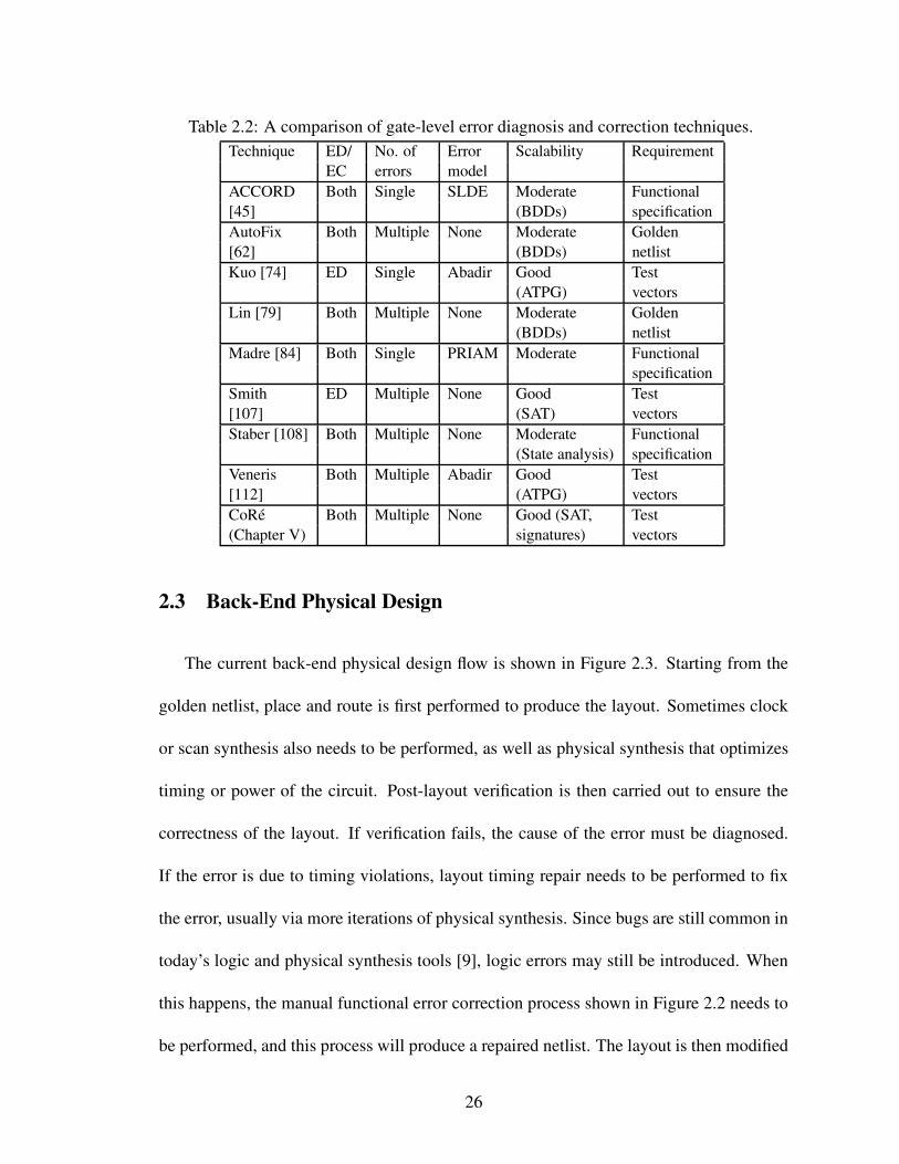
Table 2.2: A comparison of gate-level error diagnosis and correction techniques.Technique ED/ No. of Error Scalability Requirement
EC errors modelACCORD Both Single SLDE Moderate Functional[45] (BDDs) specificationAutoFix Both Multiple None Moderate Golden[62] (BDDs) netlistKuo [74] ED Single Abadir Good Test
(ATPG) vectorsLin [79] Both Multiple None Moderate Golden
(BDDs) netlistMadre [84] Both Single PRIAM Moderate Functional
specificationSmith ED Multiple None Good Test[107] (SAT) vectorsStaber [108] Both Multiple None Moderate Functional
(State analysis) specificationVeneris Both Multiple Abadir Good Test[112] (ATPG) vectorsCoRe Both Multiple None Good (SAT, Test(Chapter V) signatures) vectors
2.3 Back-End Physical Design
The current back-end physical design flow is shown in Figure 2.3. Starting from the
golden netlist, place and route is first performed to produce the layout. Sometimes clock
or scan synthesis also needs to be performed, as well as physical synthesis that optimizes
timing or power of the circuit. Post-layout verification is then carried out to ensure the
correctness of the layout. If verification fails, the cause of the error must be diagnosed.
If the error is due to timing violations, layout timing repair needs to be performed to fix
the error, usually via more iterations of physical synthesis. Since bugs are still common in
today’s logic and physical synthesis tools [9], logic errors may still be introduced. When
this happens, the manual functional error correction process shown in Figure 2.2 needs to
be performed, and this process will produce a repaired netlist. The layout is then modified
26

Figure 2.3: The current back-end physical design flow.
to reflect the change in the netlist, after which its correctness is verified again.
2.4 Post-Silicon Debugging
Figure 2.4 shows the current post-silicon debugging flow. To verify the correctness of
a silicon die, engineers apply numerous test vectors to the die and then check their output
responses. If the responses are correct for all the applied test vectors, then the die passes
verification. If not, then the test vectors that expose the design errors become the bug trace
that can be used to diagnose and correct the errors. The trace will then be diagnosed to
identify the root causes of the errors. Typically, there are three types of errors: functional,
electrical and manufacturing/yield. In this work we only focus on the first two types.
After errors are diagnosed, the layout is modified to correct them, and the repaired
27

Figure 2.4: The current post-silicon debugging flow.
layout must be verified again. This process is repeated until no more errors are exposed.
In post-silicon debugging, however, it is often unnecessary to fix all the errors because
repairing a fraction of the errors may be sufficient to enable further verification. For exam-
ple, a processor may contain a bug in its ALU and another one in its branch predictor. If
fixing the bug in the ALU is sufficient to enable further testing, then the fix in the branch
predictor can be postponed to the next respin. On the other hand, all the bugs should be
fixed before the chip is shipped to the customers.
Josephson documented the major silicon failure mechanisms in microprocessors [67],
where the most common failures (excluding dynamic logic) are drive strength (9%), logic
errors (9%), race conditions (8%), unexpected capacitive coupling (7%), and drive fights
(7%). Another important problem at the latest technology nodes are antenna effects, which
can damage a circuit during its manufacturing or reduce its reliability. These problems
often can only be identified in post-silicon debugging.
Pre-silicon and post-silicon debugging differ in several significant ways. First, con-
28

ceptual bugs that require deep understanding of the chip’s functionality are predominantly
introduced when the chip is being designed and well before the first silicon is available,
and such bugs may not be fixable by automatic tools. As Table 2.1 shows, however, com-
plex and conceptual errors only contribute to 7.9% of the errors at early design stages,
and such errors can often be caught by pre-silicon verification. As a result, post-silicon
functional bugs are mostly subtle errors that only affect the output responses of a few input
vectors, and their fixes can usually be implemented with very few gates. As an analysis
of commercial microprocessors suggests [114], faults in control logic contribute to 52%
of the total errors, which are typically subtle and only appear in rare corner-cases. How-
ever, repairing such errors requires the analysis of detailed layout information, making it
a highly tedious and error-prone task. As we show in Chapter XI, our work can automate
this process. Second, errors found post-silicon typically include functional and electrical
problems, as well as those related to manufacturability and yield. However, issues identi-
fied pre-silicon are predominantly related to functional and timing errors.2 Problems that
manage to evade pre-silicon validation are often difficult to simulate, analyze and even
duplicate. Third, the observability of the internal signals on a silicon die is extremely lim-
ited. Most internal signals cannot be directly observed, even in designs with built-in scan
chains (see Section 3.3.1) that enable access to sequential elements. Fourth, verifying the
correctness of a fix is challenging because it is difficult to physically implement a fix in a
chip that has already been manufactured. Although techniques such as FIB exist (see Sec-
tion 3.3.2), they typically can only change metal layers of the chip and cannot create any2Post-silicon timing violations are often caused by electrical problems and are only their symptoms.
29

new transistor (this process is often called metal fix).3 Finally, it is especially important
to minimize the layout area affected by each change in post-silicon debugging because
smaller changes are easier to implement with good FIB techniques, and there is a smaller
risk of unexpected side effects. Due to these unusual circumstances and constraints, most
debugging techniques prevalent in early design stages cannot be applied to post-silicon
debugging. In particular, conventional physical synthesis and ECO techniques affect too
many cells or wire segments to be useful in post-silicon debugging. As illustrated in Fig-
ure 2.5(b), a small modification in the layout that sizes up a gate requires changes in all
transistor masks and refabrication of the chip. On the other hand, our techniques are aware
of the physical constraints and can repair errors with minimal physical changes, as shown
in Figure 2.5(c).
(a) (b) (c)
Figure 2.5: Post-silicon error-repair example. (a) The original buggy layout with a weakdriver (INV). (b) A traditional resynthesis technique finds a “simple” fix thatsizes up the driving gate, but it requires expensive remanufacturing of the sil-icon die to change the transistors. (c) Our physically-aware techniques find amore “complex” fix using symmetry-based rewiring, and the fix can be imple-mented simply with a metal fix and has smaller physical impact.
To repair post-silicon functional errors, the current trend is to provide more visibil-3Despite the impressive success of the FIB technique at recent fabrication technology nodes, the use of
FIB is projected to become more problematic at future nodes, limiting how extensive changes can be andfurther complicating post-silicon debugging.
30

ity and controllability of the silicon die. For example, most modern designs incorporate
a technique, called scan test [20], into their chips. This technique allows engineers to
observe the values of internal registers and can greatly improve the design signals’ ob-
servability. In order to change the logic on a silicon die, spare cells are often scattered
throughout a design to enable metal fix [68]. The number of spare cells depends on the
methodology, as well as the expectation for respins and future steppings, and this number
can reach 1% of all cells in mass-produced microprocessor designs. Alternatively, Lin et
al. [80] proposed the use of programmable logic for this purpose. DAFCA provides a
more comprehensive solution that further improves the observability of silicon dies and
enables logic changes on the dies [2, 136]. A success story can be found in [65].
Debugging electrical errors is often more challenging than debugging functional errors
because it does not allow the deployment of logic debugging tools that designers are fa-
miliar with. In addition, there are various reasons for electrical errors [67], and analyzing
them requires profound design and physical knowledge. Although techniques to debug
electrical errors exist (e.g., voltage-frequency Shmoo plots [10]), they are often heuristic
in nature and require abundant expertise and experience. As a result, post-silicon debug-
ging is currently an art, not a science. Even if the causes of the errors can be identified,
finding valid fixes is still challenging because most existing resynthesis techniques require
changes in transistor cells and do not allow metal fix. To address this problem, techniques
that allow post-silicon metal fix have been developed recently, such as ECO routing [120].
However, ECO routing can only repair a fraction of electrical errors because it cannot find
layout transformations involving logic changes. To repair more difficult bugs, transfor-
31

mations that also utilize logic information are required. For example, one way to repair a
driving strength error is to identify alternative signal sources that also generate the same
signal, and this can only be achieved by considering logic information. All these issues
will be addressed and solved by our FogClear post-silicon debugging methodology that
we present in Chapter XI.
32

CHAPTER III
Traditional Techniques for Finding and Fixing Bugs
In the previous chapter we described the current design and verification methodolo-
gies at different design stages. In this chapter we take a closer look at the verification
techniques used in these methodologies. Among the techniques available for functional
verification, simulation-based verification is prevalent in the industry because of its lin-
ear and predictable complexity as well as its flexibility in being applied, in some form,
to any design. However, simulation can only find bugs that can be exposed by the given
stimuli. Therefore, unless all possible input scenarios can be covered by the stimuli, the
correctness of the design cannot be guaranteed. To address this problem, formal methods
have been developed to prove the correctness of the design under certain pre-defined prop-
erties. Nonetheless, their scalability is often limited because the proving process can be
very complicated. In addition, developing properties may be as difficult as developing the
design itself. Therefore, formal techniques are applied to only a small portion of the cur-
rent designs. To overcome this problem, hybrid techniques that utilize both simulation and
formal methods have been proposed. One of the contributions in our work is to leverage
the strength of both methods in an intelligent way to achieve the scalability and accu-
33

racy required in automatic error repair. In this chapter, we first review simulation-based
verification techniques. Next, we describe commonly used formal methods. Finally, we
introduce the scan chain Design-for-Debugging (DFD) construct and the metal fix tech-
nique that facilitate post-silicon debugging.
3.1 Simulation-Based Verification
Simulation is the most commonly used technique for verifying the correctness of a
design. In its simplest form, called direct test, engineers manually develop the test vectors
that are applied to the design and then inspect their output responses. Developing the test
suites, however, can be costly and time-consuming. In addition, scenarios not considered
by the designers may be overlooked by the test developers as well. Therefore, techniques
that automate testbench generation have been proposed to avoid the bias from human
engineers. A common methodology to this context is constrained-random simulation. It
involves connecting a logic simulator with stimuli coming from a constraint-based random
generator, i.e., an engine that can automatically produce random legal inputs for the design
at a very high rate based on a set of rules (or constraints) derived from the specification.
A fast simulator is the core of simulation-based verification methodologies; therefore,
in this section we review two commonly used simulation algorithms. Since the quality of
test vectors generated in constrained-random simulation greatly affects the thoroughness
of verification, we also review several solutions that improve this quality.
34

3.1.1 Logic Simulation Algorithms
Logic simulation mimics the operation of a digital circuit by calculating the outputs of
the circuit using given input stimuli. For example, if a 0 is applied to the input of an in-
verter, logic simulation will produce a 1 on its output. Algorithms that perform simulation
can be categorized into two major types: oblivious and event-driven [11]. In the oblivious
algorithm, all gates are simulated at each time point. In event-driven simulation, value
changes in the netlist are recorded, and only the gates that might cause further changes
are simulated. Event-driven algorithms are potentially more efficient than oblivious al-
gorithms because they only simulate the part of the netlist that had their values changed;
however, the overhead to keep track of the gates that should be simulated is also a concern.
A typical oblivious simulation algorithm works as follows:
1. A linear list of gates is produced by levelizing the netlist. Gates closer to the primary
inputs (i.e., those at lower levels of logic) are placed on the front of the list.
2. At each time point, all the gates in the list are simulated. Since gates with smaller
levels of logic are simulated first, the simulation values at the inputs of the gate
currently being simulated are always valid. As a result, the simulation value at the
gate’s output is also correct.
Event-driven algorithms are more complicated than oblivious ones because the algo-
rithms must keep track of the gates that need to be resimulated. One such algorithm,
proposed by Lewis [77], is shown in Figure 3.1. Two phases are used in Lewis’ algorithm,
including the node phase (also called the event phase) and the gate phase (also called the
evaluation phase).
35

1 fanout:2 foreach node ∈ active nodes3 node.val= node.next val;4 active gates = active gates∪node′s f anout gates;5 active nodes.clear();6 simulate:7 foreach gate ∈ active gates8 simulate gate;9 foreach node ∈ gate′s output
10 if (node.val != node.next val)11 active nodes=active nodes∪node;12 active gates.clear();Figure 3.1: Lewis’ event-driven simulation algorithm.
The node phase corresponds to the code labeled “fanout:”, and the gate phase corre-
sponds to the code labeled “simulate:”. There are two lists that represent the state of the
netlist: the first one is for the active nodes, while the other one is for the active gates. At
each time point, nodes in active nodes list are scanned and their fanout gates are added
to the active gates list. The logic value of each node is also updated from its next val,
and the active nodes list is cleared. The active gates list is then scanned, and each active
gate is simulated. The simulation results will be used to update the next val of the gate’s
output nodes. If the node’s new value (in node.next val) is different from its current value
(in node.val), the node will be added to the active nodes list. The active gates list is then
cleared. Since gates will be simulated only if their input values change, Lewis’ simulation
algorithm can avoid redundant computation that simulates gates whose output values will
not change.
3.1.2 Improving Test Generation and Verification
One major obstacle in adopting constrained-random simulation into the verification
flow is that writing the constraints may be difficult: the constraints need to model the
36

environment for the design under verification, and describing the environment using con-
straints can be challenging. To address this problem, Yuan et al. [123] proposed techniques
to generate the constraints using rules specified by designers. In this way, test develop-
ers can focus on describing the high-level behavior of the environment and let the tool
automatically generate the constraints. Alternatively, commercial Verification Intellectual
Properties (VIPs) and Bus Functional Models (BFMs) are also available for modeling the
test environment [126, 129].
The quality of a test suite is determined by the input scenarios that can be explored by
its tests. Test vectors that cover corner-case scenarios are often considered as of high qual-
ity. Since random simulation tends to cover scenarios that occur frequently, techniques that
try to generate tests with higher quality have been proposed. For example, the StressTest
technique [113] monitors circuit activities at key signals and uses a Markov-model-driven
test generator to cover the corner-case scenarios. Shimizu et al. [106] took another ap-
proach by deriving an input generator and a coverage metric from a formal specification
first, and then they used the measured coverage to bias the input generator. Recent work
by Plaza et al. [93] measures signal activities based on Shannon entropy and uses the
measured activities to guide a pattern generator to produce high-quality test vectors.
3.2 Formal Verification
Simulation-based verification uses a large number of input vectors to check a design’s
responses. Due to the scalability of modern simulators, whole-chip simulation can often
be performed. However, it is usually infeasible to simulate all possible input sequences
because the number of the sequences is typically large and can even be infinite. As a result,
37

it is difficult to judge whether all possible scenarios have been covered, making complete
verification difficult.
Formal verification is a totally different approach. It uses mathematical methods to
prove or disprove the correctness of the design with respect to a certain formal specifi-
cations or properties. In this way, complete verification can be achieved to the extent
described by the specification or properties. However, the complexity of formally veri-
fying a design grows considerably with the size of the circuit, making formal techniques
applicable to smaller designs only. As a result, currently it is often used to verify small
and critical components within a large design.
In this section we first describe a commonly used problem formulation, the SATisfi-
ability (SAT) problem. Next, we briefly introduce several formal verification techniques,
including Bounded Model Checking (BMC), symbolic simulation, reachability analysis
and equivalence checking.
3.2.1 Satisfiability Problem
A SATisfiability (SAT) problem can be formulated as follows. Given a Boolean ex-
pression composed of AND, OR, NOT, variables and parentheses, determine if there is an
assignment of true and false values to the variables that makes the expression evaluate to
true. If no such assignment exists, then the expression is said to be unsatisfiable. Other-
wise, the expression is satisfiable, and the assignment is a solution to the SAT problem. If
the Boolean expression is a conjunction (AND) of clauses, then we call it a Conjunctive
Normal Form (CNF). Since netlists composed of logic gates can be converted into CNF
easily, SAT has been used extensively to solve circuit design and verification problems.
38

SAT is the first known NP-complete problem [47]. Fortunately, many practical SAT
problems can be solved by modern solvers such as MiniSat [51], GRASP [85] and zChaff
[90]. However, these solvers still cannot handle many important problems, and more
research on this problem is being conducted.
3.2.2 Bounded Model Checking
Bounded Model Checking (BMC) [15] is a formal method which can prove or dis-
prove properties of bounded length in a design, frequently using SAT solving techniques
to achieve this goal. A high-level flow of the algorithm is given in Figure 3.2. The central
idea of BMC is to “unroll” a given sequential circuit k times to generate a combinational
circuit that has behavior equivalent to k clock cycles of the original circuit. In the process
of unrolling, the circuit’s memory elements are eliminated, and the signals that feed them
at cycle i are connected directly to the memory elements’ output signals at cycle i− 1.
In CNF-based SAT, the resulting combinational circuit is converted to a CNF formula C.
The property to be proved is also complemented and converted to CNF form (p). These
two formulas are conjoined and the resulting SAT instance I is fed into a SAT solver. If a
satisfiable assignment is found for I, then the assignment describes a counterexample that
falsifies the (bounded) property, otherwise the property holds true.
1 SAT-BMC(circuit, property,maxK)2 p= CNF(!property);3 for k=1 to maxK do4 C = CNF(unroll(circuit,k));5 I = C∧ p; //SAT instance6 if (I is satisfiable)7 return (SAT solution);
Figure 3.2: Pseudo-code for Bounded Model Checking.
39

3.2.3 Symbolic Simulation
The basic idea behind symbolic simulation is similar to that of logic simulation [13].
Unlike logic simulation, however, Boolean variables are simulated instead of constant
scalar values. For example, simulating “A AND B” will produce a Boolean expression
representing “A AND B” instead of a Boolean value.
In symbolic simulation, a new symbol is injected to each primary input at each cycle.
Symbolic simulation then produces Boolean expressions at the outputs of the circuit using
the injected symbols. Since each symbol implicitly represents both the values 1 and 0,
the generated Boolean expressions represent all possible input sequences. As a result, if
the design has n inputs, symbolic simulation can produce outputs representing all 2n input
patterns in one single step. Traditionally, Binary Decision Diagrams (BDDs) [18] have
been used to represent the Boolean expressions due to their flexibility in Boolean manip-
ulations. Recently, symbolic simulators using CNF to represent the Boolean expressions
have also been developed [126].
The verification power of symbolic simulation is similar to that of BMC: it can be used
to prove properties within a bounded number of cycles or disprove a property; however,
it cannot prove a property that considers an indefinite number of cycles. For example,
symbolic simulation can falsify a property like “c1 is always equal to 0”, or it can prove
a property like “c1 always becomes 1 three cycles after a1 is set to 0”. Nonetheless, it
cannot prove a property that says “c1 is always equal to 0”.
40

3.2.4 Reachability Analysis
Reachability analysis is also called symbolic traversal or least fix-point computation.
It tries to solve the following problem: given a Finite State Machine (FSM) description
of a sequential digital circuit, find all the reachable states from a set of initial states. Its
algorithmic flow is shown in Figure 3.3. In the algorithm, R is a set of reached states, I
is the set of initial states, and ∆ is the transition function for the FSM (i.e., it maps each
(state, input) to a next state). We use subscript t to represent the cycle at which the current
computation takes place. The Img function used in the algorithm calculates the forward
image of the given states and transition functions. To this end, Coudert et al. [48] provide
an efficient algorithm for forward-image computation.
1 t= 0;2 Rt = I; // Start from initial state3 repeat4 Rt+1 = Rt ∪ Img(Rt ,∆); // Compute forward image5 until (Rt+1 == Rt ); // Repeat until a fix point is reached
Figure 3.3: The algorithmic flow of reachability analysis.
Reachability analysis possesses greater verification power than BMC and symbolic
simulation in that it can prove properties that consider an infinite number of cycles. To
prove properties using reachability analysis, we first identify the set of states P′ that do
not satisfy the property. Next, we compute the reachable set R. If we found that R∩P′ is
empty, then the property holds; otherwise, the property can be violated and there is a bug.
Although reachability analysis is powerful, representing the states is challenging be-
cause the number of possible states grows exponentially with the number of state bits.
Although BDDs have been shown to be effective in encoding the states, their scalability
41

is still limited. To address this problem, several different approaches have been proposed,
including abstraction, parameterization and mixed traversal algorithms [97].
3.2.5 Equivalence Checking
The purpose of equivalence checking is to prove that two circuits exhibit exactly the
same behavior. There are two types of equivalency between two circuits: combinational
and sequential. Given identical input vectors, combinational equivalency requires both
circuits to produce exactly the same responses at their primary outputs and register bound-
aries. On the other hand, sequential equivalency only requires the responses at primary
outputs to be identical.
The basic procedure to perform combinational equivalence checking between two cir-
cuits works as follows. First, the inputs/outputs to the registers are broken into primary
outputs/inputs of the circuits. Next, a miter is added between each pair of correspond-
ing outputs, where a miter is a circuit consisting of an XOR gate combining the pair of
outputs. Third, the corresponding inputs between two circuits are connected to the same
signal sources. After inserting these constructs, the equivalence checker then tries to find
an input pattern that makes the output of any of the inserted miters 1. If no such pattern can
be found, then the two circuits are equivalent; otherwise they are not equivalent and the
pattern is a counterexample. The equivalence checker can be implemented using BDDs
or CNF-SAT. Techniques that improve this basic procedure have also been proposed, for
example [73].
BMC can be used to perform sequential equivalence checking up to a certain number
of cycles C, and it works as follows. Given two circuits, they are first unrolled C times.
42

Next, the primary inputs of both circuits for each unrolled copy are connected, and the
circuits are constrained using their initial states. Miters are then added to the unrolled
primary outputs between both circuits. BDDs or CNF-SAT can then be used to perform
the checking. If a sequence of patterns exists that can make the output of any miter 1, then
the circuits are not sequentially equivalent, and the sequence becomes a counterexample.
3.3 Design for Debugging and Post-Silicon Metal Fix
Post-silicon debugging is considerably different from pre-silicon debugging because of
its special physical constraints. In particular, observing, controlling and changing any cir-
cuit component post-silicon is very difficult. To address this problem, existing techniques
focus on improving the observability and controllability of the silicon die. In this section
we describe the most commonly-used DFD construct, scan chains. Next, we introduce the
Focused Ion Beam (FIB) technique that supports post-silicon metal fix.
3.3.1 Scan Chains
Without special constructs, only the values of a circuit’s primary inputs and outputs can
be observed and controlled. Therefore, modern chips often use scan chains [20] to improve
the design’s observability and controllability. The basic idea behind scan chains is to
employ sequential elements that have a serial shift capability so that they can be connected
to form long shift registers. The scan-chain elements, as shown in Figure 3.4, can then
operate like primary inputs or outputs during debugging, which can greatly improve the
controllability and observability of the circuit’s internal signals.
43

Figure 3.4: The BILBO general-purpose scan-chain element.
3.3.2 Post-Silicon Metal Fix via Focused Ion Beam
FIB is a technique that uses a focused beam of gallium ions [86]. Gallium is chosen
because it is easy to liquefy and ionize. After gallium is liquefied, a huge electric field
causes ionization and field emission of the gallium atoms, and the ions are focused onto
the target by electrostatic lens. When the high-energy gallium ions strike their target,
atoms will be sputtered from the surface of the target. Because of this, FIB is often used as
a micro-machining tool to modify materials at the nanoscale level. In the semiconductor
industry, FIB can be applied to modify an existing silicon die. For example, it can cut
a wire or deposit conductive material in order to make a connection. However, it cannot
create new transistors on a silicon die.
To remove unwanted materials from a silicon die, ion milling is used. When an ac-
celerated ion hits the silicon die, the ion loses its energy by scattering the electrons and
the lattice atoms. If the energy is higher than the binding energy of the atoms, the atoms
will be sputtered from the surface of the silicon die. To complement material removal,
ion-induced deposition is used to add new materials to a silicon die. In the process, a pre-
cursor gas, often an organometallic, is directed to and absorbed by the surface of the die.
When the incident ion beam hits the gas molecule, the molecule dissociates and leaves the
44

metal constituent as a deposit. Similarly, insulator can also be deposited on the die. Since
impurities such as gallium ions may be trapped by the deposited materials, the conductiv-
ity/resistivity of the deposited metal/insulator tends to be worse than that produced using
the regular manufacturing process. Fortunately, this phenomenon does not pose serious
challenges in post-silicon debugging because the changes made are typically small.
FIB can either cut or reconnect top-level wires. Changing metallic wires at lower
levels, however, is a much more elaborate process. To achieve this, a large hole is first
milled through the upper-level wires to expose the lower-level wire, then the hole is filled
with oxide for insulation. Next, a new smaller hole is milled through the refilled oxide,
and metal is deposited down to the lower level. The affected upper-level wires may need
to be reconnected in a similar way. An illustration of the process is shown in Figure 3.5.
(1) (2) (3) (4)
Figure 3.5: Schematic showing the process to connect to a lower-level wire through anupper-level wire: (a) a large hole is milled through the upper level; (b) the holeis filled with SiO2; (c) a smaller hole is milled to the lower-level wire; and (d)the hole is filled with new metal. In the figure, whitespace is filled with SiO2,and the dark blocks are metal wires.
45

PART II
FogClear Methodologies andTheoretical Advances in Error Repair
46

CHAPTER IV
FogClear: Circuit Design and Verification Methodologies
In this chapter we describe our FogClear methodologies that automate the IC verifi-
cation and debugging flows, including front-end design, back-end logic design, back-end
physical design and post-silicon debugging.
4.1 Front-End Design
Our FogClear front-end methodology automates the functional error correction pro-
cess, and it works as follows. Given a bug trace and the RTL model that fails verification,
Butramin (see Chapter VIII) is used to minimize the bug trace, and then the minimized bug
trace is analyzed by the REDIR framework (see Section 9.2) to produce a repaired RTL
model. The repaired RTL model is verified again to make sure no new bugs are introduced
by the fix. This process keeps repeating until the model passes verification. The FogClear
front-end design flow is shown in Figure 4.1, where the “Automatic functional error cor-
rection” block replaces the “Manual functional error correction” block in Figure 2.1. By
automating the error diagnosis and correction process, engineers’ time can be saved, and
design quality can be improved.
47

Figure 4.1: The FogClear front-end design flow.
4.2 Back-End Logic Design
Fixing errors at the gate level is more difficult than at the RTL because engineers
are unfamiliar with the synthesized netlists. In order to address this problem, our Fog-
Clear design flow automatically repairs the gate-level netlist. As shown in Figure 4.2, it
is achieved by analyzing the counterexamples returned by the verification engine using
the CoRe framework (see Chapter V and Section 9.1). This framework automates the
gate-level error-correction process and thus saves engineers’ time and effort.
48

Figure 4.2: The FogClear back-end logic design flow.
4.3 Back-End Physical Design
Due to the growing dominance of interconnect in delay and power of modern designs,
tremendous physical synthesis effort and even more powerful optimizations such as retim-
ing are required. Given that bugs still appear in many EDA tools today [9], it is important
to verify the correctness of the performed optimizations. Traditional techniques address
this verification problem by checking the equivalence between the original design and the
optimized version. This approach, however, only verifies the equivalence of two versions
of the design after a number, or possibly all, of the transformations and optimizations
have been completed. Unfortunately, such an approach is not sustainable in the long term
because it makes the identification, isolation, and correction of errors introduced by the
transformations extremely difficult and time-consuming. On the other hand, performing
49

traditional equivalence checking after each circuit transformation is too demanding. Since
functional correctness is the most important aspect of high-quality designs, a large amount
of effort is currently devoted to verification and debugging, expending resources that could
have otherwise been dedicated to improve other aspects of performance. To this end, ver-
ification has become the bottleneck that limits achievable optimizations and the features
that can be included in a design [42], slowing down the evolution of the overall quality of
electronic designs.
Figure 4.3: The FogClear back-end physical design flow.
The FogClear back-end physical design flow shown in Figure 4.3 addresses this prob-
lem using an incremental verification system called InVerS, which will be described in
detail in Chapter X. InVerS relies on a metric called similarity factor to point out the
50

changes that might have corrupted the circuit. Since this metric is calculated by fast simu-
lation, it can be applied after every circuit modification, allowing engineers to know when
a bug might have been introduced and traditional verification should be performed. When
the similarity factor indicates a potential problem, traditional verification should be per-
formed to check the correctness of the executed circuit modification. If verification fails,
the CoRe framework can be used to repair the errors. Alternatively, the errors can also be
fixed by reversing the performed modification.
As Section 10.3 shows, the InVerS system has high accuracy and can catch most errors.
However, it is still possible that a few errors may escape incremental verification and be
found in the full-fledged post-layout verification. When this happens, the post-silicon
error-repair techniques that we describe in the next section can be used to repair the layout
and fix the errors.
4.4 Post-Silicon Debugging
Figure 4.4 shows our FogClear methodology which automates post-silicon debugging.
When post-silicon verification fails, a bug trace is produced. Since silicon dies offer simu-
lation speed orders of magnitude faster than that provided by logic simulators, constrained-
random testing is used extensively, generating extremely long bug traces. To simplify error
diagnosis, we also apply bug trace minimization in our methodology to reduce the com-
plexity of traces using the Butramin technique.
After a bug trace is simplified, we simulate the trace with a logic simulator using the
source netlist for the design layout. If simulation exposes the error, then the error is func-
tional, and PAFER is used to generate a repaired layout; otherwise, the error is electrical.
51

Currently, we still require manual error diagnosis to find the cause of an electrical error.
After the cause of the error is identified, we check if the error can be repaired by ECO
routing. If so, we apply existing ECO routing tools such as those in [120]; otherwise, we
use SymWire or SafeResynth to change the logic and wire connections around the error
spot in order to fix the problem. The layout generated by SymWire or SafeResynth is then
routed by an ECO router to produce the final repaired layout. This layout can be used to
fix the silicon die for further verification. A more detailed description on the components
used in our flow is given in Chapter XI.
Figure 4.4: The FogClear post-silicon debugging flow.
52

CHAPTER V
Counterexample-Guided Error-Repair Framework
In this chapter we present a resynthesis framework, called CoRe, that automatically
corrects errors in combinational gate-level designs. The framework is based on a novel
simulation-based abstraction technique and utilizes resynthesis to modify the functional-
ity of a circuit’s internal nodes to match the correct behavior. Compared with previous
solutions, CoRe is more powerful in that: (1) it can fix a broader range of error types
because it is not bounded by specific error models; (2) it derives the correct functional-
ity from simulation vectors, without requiring golden netlists; and (3) it can be applied
with a broad range of verification flows, including formal and simulation-based. In this
chapter, we first provide required background. Next, we present our CoRe framework that
addresses the gate-level error-repair problem.
5.1 Background
In CoRe we assume that an input design, with one or more bugs, is provided as a
Boolean network. We strive to correct its erroneous behavior by regenerating the func-
tionality of incorrect nodes. This section starts by defining some terminology and then
overviews relevant background.
53

5.1.1 Signatures
Definition 1 Given a node t in a Boolean network, whose function is f , as well as input
vectors x1, x2 ... xk. We define the signature of node t, st , as ( f (x1), ..., f (xk)), where
f (xi) ∈ 0,1 represents the output of f given an input vector xi.
Our goal is to modify the functions of the nodes responsible for the erroneous behavior
of a circuit via resynthesis. In this context, we call a node to be resynthesized the target
node, and we call the nodes that we can use as inputs to the newly synthesized node (func-
tion) the candidate nodes. Their corresponding signatures are called the target signature
and the candidate signatures, respectively.
Given a target signature st and a collection of candidate signatures sc1 , sc2 ,...,scn , we say
that st can be resynthesized by sc1 , sc2 ,...,scn if st can be expressed as st= f (sc1,sc2, ...,scn),
where f (sc1,sc2, ...,scn) is a vector Boolean function called the resynthesis function. We
also call a netlist that implements the resynthesis function the resynthesized netlist.
5.1.2 Don’t-Cares
When considering a subnetwork within a large Boolean network, Don’t-Cares (DCs)
are exploited by many synthesis techniques because they provide additional freedom for
optimizations. Satisfiability Don’t-Cares (SDCs) occur when certain combinations of input
values do not occur for the subnetwork, while Observability Don’t-Cares (ODCs) occur
when the output values of the subnetwork do not affect any primary output. As we show
in Section 5.2.1, our CoRe framework is able to utilize both SDCs and ODCs.
54

5.1.3 SAT-Based Error Diagnosis
The error-diagnosis technique used in our CoRe framework is based on the work by
Smith et al. [107]. Given a logic netlist, a set of test vectors and a set of correct output
responses, this technique will return a set of wires, also called error sites, along with their
values for each test vector that can correct the erroneous output responses. Our CoRe
framework then corrects design errors by resynthesizing the error sites using the corrected
values as the target signatures. In Smith’s error-diagnosis technique, three components
are added to the netlist, including (1) multiplexers, (2) test-vector constraints, and (3)
cardinality constraints. The whole circuit is then converted to CNF, and a SAT solver
is used to perform error diagnosis. These components are added temporarily for error
diagnosis only and will not appear in the netlist produced by CoRe. They are described in
detail below.
(a) (b)Figure 5.1: Error diagnosis. In (a) a multiplexer is added to model the correction of an
error, while (b) shows the error cardinality constraints that limit the number ofasserted select lines to N.
A multiplexer is added to every wire to model the correction of the erroneous netlist.
When the select line is 0, the original driver of the wire is used. When the select line
is 1, the multiplexer chooses a new signal source instead, and the values applied by the
55

new source will correct the erroneous output responses. An example of the multiplexer is
given in Figure 5.1(a). A variable, vi, is introduced for every multiplexer to model the new
source to the wire.
Test-vector constraints are used to force the erroneous netlist to produce correct output
responses for the test vectors. Obviously, the netlist can produce correct output responses
only if a subset of the select lines of the added multiplexers are set to 1, allowing the cor-
responding new signal sources to generate logic values that agree with the signal sources
which produce the correct responses. These constraints are implemented by duplicating
one copy of the multiplexer-enriched netlist for each test vector. The inputs of the copy
are controlled by the test vector, and its outputs are constrained by the correct responses.
Cardinality constraints restrict the number of select lines that can be set to 1 simultane-
ously. This number also represents the number of error sites in the netlist. The cardinality
constraints are implemented by an adder which performs a bitwise addition of the select
lines, and a comparator which forces the sum of the adder to be N, as shown in Figure
5.1(b). Initially, N is set to 1, and error diagnosis is performed by incrementing N until a
solution is found.
5.1.4 Error Model
To tame the enormous complexity of error diagnosis and correction, several error mod-
els have been introduced. These models classify common design errors in order to reduce
the difficulty of repairing them. Here we describe a frequently used model formulated by
D. Nayak [91], which is based on Abadir’s model [1].
In the model, type “a” (wrong gate) mistakenly replaces one gate type by another one
56

Figure 5.2: Errors modeled by Abadir et al. [1].
with the same number of inputs; types “b” and “c” (extra/missing wire) use a gate with
more or fewer inputs than required; type “d” (wrong input) connects a gate input to a
wrong signal; and types “e” and “f” (extra/missing gate) incorrectly add or remove a gate.
An illustration of the model is given in Figure 5.2.
5.2 Error-Correction Framework for Combinational Circuits
For the discussion in this section we restrict our analysis to combinational designs.
In this context, the correctness of a circuit is simply determined by the output responses
under all possible input vectors. We will show in Section 9.1 how to extend the framework
to sequential designs.
CoRe, our error-correction framework, relies on simulation to generate signatures,
which constitute our abstract model of the design and are the starting point for the er-
ror diagnosis and resynthesis algorithms. After the netlist is repaired, it is checked by
a verification engine. If verification fails, possibly due to new errors introduced by the
correction process, new counterexamples are generated and used to further refine the ab-
57

straction. Although in our implementation we adopted Smith’s error-diagnosis technique
[107] due to its scalability, alternative diagnosis techniques can be used as well.
5.2.1 The CoRe Framework
In CoRe, an input test vector is called a functionality-preserving vector if its output
responses comply with the specification, and the vector is called an error-sensitizing vector
if its output responses differ. Error-sensitizing vectors are often called counterexamples.
The algorithmic flow of CoRe is outlined in Figure 5.3. The inputs to the frame-
work are the original buggy netlist (CKTerr), the initial functionality-preserving vectors
(vectorsp) and the initial error-sensitizing vectors (vectorse). The output is the recti-
fied netlist CKTnew. The framework first performs error diagnosis to identify error lo-
cations and the correct values that should be generated for those locations so that the
error-sensitizing vectors could produce the correct output responses. Those error locations
constitute the target nodes for resynthesis. The bits in the target nodes’ signatures that
correspond to the error-sensitizing vectors must be corrected according to the diagnosis
results, while the bits that correspond to the functionality-preserving vectors must remain
unchanged. If we could somehow create new combinational netlist blocks that gener-
ate the required signatures at the target nodes using other nodes in the Boolean network,
we would be able to correct the circuit’s errors, at least those that have been exposed
by the error-sensitizing vectors. Let us assume for now that we can create such netlists
(techniques to this end will be discussed in the next chapter), producing the new circuit
CKTnew (line 4). CKTnew is checked at line 5 using the verification engine. When verifi-
cation fails, new error-sensitizing vectors for CKTnew will be returned in counterexample.
58

If no such vector exists, the circuit has been successfully corrected and CKTnew is re-
turned. Otherwise, CKTnew is abandoned, while counterexample is classified either as
error-sensitizing or functionality-preserving with respect to the original design (CKTerr).
If counterexample is error-sensitizing, it will be added to vectorse and be used to re-
diagnose the design. CKTerr’s signatures are then updated using counterexample. By
accumulating both functionality-preserving and error-sensitizing vectors, CoRe will avoid
reproposing the same wrong correction; hence guaranteeing that the algorithm will even-
tually complete. Figure 5.4 illustrates a possible execution scenario with the flow that we
just described.
CoRe(CKTerr,vectorsp,vectorse,CKTnew)1 compute signatures(CKTerr,vectorsp,vectorse);2 f ixes= diagnose(CKTerr,vectorse);3 foreach f ix ∈ f ixes4 CKTnew= resynthesize(CKTerr, f ix);5 counterexample=veri f y(CKTnew);6 if (counterexample is empty) return CKTnew;7 else if (counterexample is error-sensitizing for CKTerr)8 vectorse = vectorse∪ counterexample;9 f ixes= rediagnose(CKTerr,vectorse);
10 update signatures(CKTerr,counterexample);Figure 5.3: The algorithmic flow of CoRe.
(1) (2) (3)Figure 5.4: Execution example of CoRe. Signatures are shown above the wires, where
underlined bits correspond to error-sensitizing vectors. (1) The gate was meantto be AND but is erroneously an OR. Error diagnosis finds that the output ofthe 2nd pattern should be 0 instead of 1; (2) the first resynthesized netlistfixes the 2nd pattern, but fails further verification (the output of the 3rd patternshould be 1); (3) the counterexample from step 2 refines the signatures, and aresynthesized netlist that fixes all the test patterns is found.
59

SDCs are exploited in CoRe by construction because simulation can only produce legal
signatures. To utilize ODCs, we simulate the complement signature of the target node and
mark the bit positions whose changes do not propagate to any primary output as ODCs:
those positions are not considered during resynthesis. Note that if a diagnosis contains
multiple error sites, the sites that are closer to primary outputs should be resynthesized
first so that the downstream logic of a node is always known when ODCs are calculated.
5.2.2 Analysis of CoRe
CoRe is more effective than many previous solutions because it supports the use of
SDCs and ODCs, including external DCs. External SDCs can be exploited by providing
only legal input patterns when generating signatures, while external ODCs are utilized by
marking uninterested output vectors don’t-cares.
To achieve the required scalability to support the global implications of error correc-
tion, CoRe uses an abstraction-refinement scheme: signatures provide an abstraction of
the Boolean network for resynthesis because they are the nodes’ partial truth tables (all
unseen input vectors are considered as DCs), and the abstraction is refined by means of
the counterexamples that fail verification. The following proposition shows that in theory,
CoRe can eventually always produce a netlist which passes verification. However, as it
is the case for most techniques based on abstraction and refinement, the framework may
time-out before a valid correction is found in practice. The use of high-quality test vectors
[112] is effective in alleviating this potential problem.
Proposition 1 Given a buggy combinational design and a specification that defines the
output responses of each input vector, the CoRe algorithm can always generate a netlist
60

that produces the correct output responses.
Proof: Given a set of required ”fixes”, the resynthesis function of CoRe can always
generate a correct set of signatures, which in turn produce correct responses at primary
outputs. Observe that each signature represents a fragment of a signal’s truth table. There-
fore, when all possible input patterns are applied to our CoRe framework, the signatures
essentially become complete truth tables, and hence define all the terms required to gen-
erate correct output responses for any possible input stimulus. In CoRe, all the counterex-
amples that fail verification are used to expand and enhance the set of signatures. Each
correction step of CoRe guarantees that the output responses of the input patterns seen
so far are correct, thus any counterexample must be new. However, since the number of
distinct input patterns is finite (at most 2n for an n-input circuit), eventually no new vec-
tor can be generated, guaranteeing that the algorithm will complete in a finite number of
iterations. In practice, we find that a correct design can often be found in a few iterations.
5.2.3 Discussions
Several existing techniques, such as those in [112], also use simulation to identify
potential error-correction options and rely on further simulation to prune unpromising
candidates. Compared with these techniques, our framework is more flexible because
it performs abstraction and refinement on the design itself. As a result, this framework
can easily adopt new error diagnosis or correction techniques. For example, our error-
correction engine can be easily replaced by any synthesis tool that can handle truth tables
or cubes. Most existing techniques, however, do not have this flexibility. On the other
61

hand, recent work by Safarpour et al. [101] provides another abstraction-refinement error-
repair methodology for sequential circuits by replacing a fraction of the registers with
primary inputs. Their methodology can be used to accelerate the diagnosis process in our
error-repair method for sequential circuits, which is described in Section 9.1.
5.2.4 Applications
CoRe can be used whenever the output responses of a netlist need to be changed. We
now develop applications of our techniques in three different verification contexts.
Application 1: combinational equivalence checking and enforcement. This appli-
cation fixes an erroneous netlist so that it becomes equivalent to a golden netlist. In this
application, the verification engine is an equivalence checker. Test vectors on which the
erroneous circuit and the golden model agree are functionality-preserving vectors, and the
remaining test vectors are error-sensitizing. Initial vectors can be obtained by random
simulation or equivalence checking.
Application 2: fixing errors found by simulation. This application corrects design
errors that break a regression test. In this application, the verification engine is the simu-
lator and the regression suite. Test vectors that break the regression are error-sensitizing
vectors, and all other vectors are functionality-preserving vectors. Initial vectors can be
obtained by collecting the inputs applied to the netlist while running the regression.
Application 3: fixing errors found by formal verification. This application assumes
that a formal tool proves that a property can be violated, and the goal is to fix the netlist
to prevent the property from being violated. In this application, counterexamples returned
by the tool are error-sensitizing vectors.
62
CHAPTER VI
Signature-Based Resynthesis Techniques
he basis for CoRe’s resynthesis solution is the signature available at each internal cir-
cuit node, where the signature of a node is essentially its partial truth table. The resynthesis
problem is formulated as follows: given a target signature, find a resynthesized netlist that
generates the target signature using the signatures of other nodes in the Boolean network
as inputs. In this Chapter, we first describe the concept of Pairs of Bits to be Distin-
guished (PBDs), which compactly encode resynthesis information. Next, we describe our
Distinguishing-Power Search (DPS) and Goal-Directed Search (GDS) resynthesis tech-
niques that are based on signatures.
6.1 Pairs of Bits to be Distinguished (PBDs)
In this section we propose the concepts of Pairs of Bits to be Distinguished (PBDs) and
distinguishing power. PBDs can be derived easily using signatures and compactly encode
the information required for resynthesis. A similar concept, Sets of Pairs of Functions to
be Distinguished (SPFDs) [105, 121, 122], is also described.
63

6.1.1 PBDs and Distinguishing Power
Recall that a signature s is a collection of the corresponding node’s simulation values.
In this chapter, we use s[i] to denote the i-th bit of signature s. The goal of error correction
is to modify the functions of the nodes responsible for the erroneous behavior of a circuit
via resynthesis. In this context, we call a node to be resynthesized the target node, and
we call the nodes that we can use as inputs to the newly synthesized node (function) the
candidate nodes. Their corresponding signatures are called the target signature and the
candidate signatures, respectively.
The proposition below states that a sufficient and necessary condition for a resynthesis
function to exist is that, whenever two bits in the target signature are distinct, then such
bits need to be distinct in at least one of the candidate signatures. This proposition is a
special case of Theorem 5.1 in [88], where the minterms appearing in signatures represent
the care-terms and all other minterms are Don’t-Cares (DCs).
Proposition 2 Consider a collection of candidate signatures, sc1 , sc2 ,...,scn , and a target
signature, st . Then a resynthesis function f , where st = f (sc1 , sc2 ,...,scn), exists if and only
if no bit pair i, j exists such that st [i] 6= st [ j] but sck [i] = sck [ j] for all 1 ≤ k ≤ n.
In this work we call a pair of bits i, j in st , where st [i] 6= st [ j], a Pair of Bits to be
Distinguished (PBD). Based on Prop. 2, we say that the PBD i, j can be distinguished
by signature sck if sck [i] 6= sck [ j]. We define the Required Distinguishing Power (RDP)
of the target signature st , RDP(st), as the set of PBDs that need to be distinguished. We
also define the Distinguishing Power (DP) of a candidate signature sck with respect to the
target signature st , DP(sck,st), as the set of PBDs in st that can be distinguished by sck .
64

With this definition, Prop. 2 can be restated as “a resynthesis function, f , exists if and only
if RDP(st) ⊆ ∪nk=1DP(sck,st)”.
6.1.2 Related Work
SPFD [105, 121, 122] is a relatively new data structure that encodes resynthesis infor-
mation and allows the use of DCs. An SPFD [121] Rt for a target node t, represented as
(g1a,g1b),(g2a,g2b), ...,(gna,gnb), denotes a set of pairs of functions that must be dis-
tinguished. In other words, for each pair (gia,gib) ∈ Rt , the minterms in gia must produce
a different value from the minterms in gib at the output of t. Assume that node t has m
fanins, c1...cm, and their SPFDs are Rc1...Rcm, then according to [122]:
Rt ⊆ ∪mi=1Rci(6.1)
In other words, the SPFD of node t is a subset of the union of all the SPFDs of its
fanins c1...cm. Since a function f satisfies an SPFD Rt if and only if for each (gia,gib) ∈
Rt , f (gia) 6= f (gib) [121]. This criterion, combined with Equation 6.1, essentially states
that a resynthesis function f exists if and only if all the minterms that need to be distin-
guished in Rt must be distinguished by at least one of its fanins, which is consistent with
Prop. 2. As a result, our use of PBDs is equivalent to SPFDs. However, our approach has
the following advantages over SPFD-based techniques:
1. PBDs provide a much more compact logic representation than SPFDs. Traditionally,
SPFDs are calculated using BDDs and suffer memory explosion problems. Recent
work represent SPFDs as graphs [105] and SAT/simulation can be used to calculate
SPFDs [88]. This approach is more memory efficient but may become computation-
65
ally expensive. On the other hand, our approach only uses signatures of nodes. Since
each minterm needs only one bit in a signature, our representation is very compact.
2. Calculating PBDs is significantly easier than calculating SPFDs: signatures are gen-
erated by simulation, and DCs are calculated by simulating the complement of the
target signature. PBDs can then be derived easily by considering only the care-terms
in the target signature.
6.2 Resynthesis Using Distinguishing-Power Search
In this section, we first define the absolute distinguishing power |DP(s)| of a signature
s, and then we propose a Distinguishing-Power Search (DPS) technique that uses |DP| to
select candidate signatures and generates the required resynthesized netlist.
6.2.1 Absolute Distinguishing Power of a Signature
Absolute distinguishing power provides search guiding and pruning criteria for our
resynthesis techniques. To simplify bookkeeping, we reorder bits in every signature so
that in the target signature all the bits with value 0 precede the ones with value 1, as in
“00...0011...11”.
Definition 2 Assume a target signature st is composed of x 0s followed by y 1s, we define
the absolute required distinguishing power of st , denoted by |RDP(st)|, as the number of
PBDs in st and equals to xy. Moreover, if a candidate signature sc has p 0s and q 1s in
its first x bit positions, and r 0s and s 1s in the remaining y positions, then we define the
absolute distinguish power of sc with respect to st , denoted by |DP(sc,st)|, as the number
of PBDs in st that can be distinguished by sc and equals to ps+qr.
66

The following corollary states a necessary but not sufficient condition to determine
whether the target signature can be generated from a collection of candidate signatures.
Corollary 1 Consider a target signature st and a collection of candidate signatures sc1...scn.
If st can be generated by sc1...scn, then |RDP(st)| ≤ ∑ni=1 |DP(sci,st)|.
Proof: By contradiction. Suppose that a resynthesis function exists and it can gen-
erate st using a collection of signatures (denoted as SC), where the total absolute distin-
guishing power of SC with respect to st (denoted as |DP(SC,st)|) is smaller than |RDP(st)|.
Since |RDP(st)| represents the number of PBDs in st and |DP(SC,st)| represents the num-
ber of PBDs distinguishable by SC, the fact that |DP(SC,st)| is smaller than |RDP(st)|
means certain PBDs in st can not be distinguished by signatures in SC. However, Prop. 2
states that for a valid resynthesis function to exist, all the PBDs in st must be distinguished.
Therefore the resynthesis function cannot exist — a contradiction.
6.2.2 Distinguishing-Power Search
Distinguishing-Power Search (DPS) is based on Prop. 2, which states that a resynthesis
function can be generated when a collection of candidate signatures covers all the PBDs
in the target signature. However, the number of collections satisfying this criterion may
be exponential in the number of total signatures. To identify possible candidate signatures
effectively, we first select signatures that cover the least-covered PBDs, second those that
have high absolute distinguishing power (i.e., signatures that cover the most number of
PBDs), and third those that cover any remaining uncovered PBD. For efficiency, we limit
the search pool to the 200 nodes which are topologically closest to the target node; how-
67

ever, we may go past this limit when those are not sufficient to cover all the PBDs in the
target signature. Finally, we exclude from the pool those nodes that are in the fanout cone
of the target node, so that we avoid creating a combinational loop inadvertently.
After the candidate signatures are selected, a truth table for the resynthesis function is
built from the signatures, and it is constructed as follows. Note that although we may select
more signatures than needed for resynthesis, the logic optimizer we use in the next step is
usually able to identify the redundant signatures and use only those which are essential.
1. Each signature is an input to the truth table. The i-th input produces the i-th column
in the table, and the j-th bit in the signature determines the value of the j-th row.
2. If the j-th bit of the target signature is 1, then the j-th row is a minterm; otherwise
it is a maxterm.
3. All other terms are don’t-cares.
Figure 6.1 shows an example of the constructed truth table. The truth table can be
synthesized and optimized using existing software, such as Espresso [99] or MVSIS [54].
Note that our resynthesis technique does not require that the support of the target function
is known a priori, since the correct support will be automatically selected when DPS
searches for a set of candidate signatures that distinguish all the PBDs. This is in contrast
with other previous solutions which require that the support of the target node to be known
before attempting to synthesize the function.
68

Signature Truth tablest=0101 s1 s2 s3 s4 sts1=1010 1 0 1 0 0s2=0101 0 1 1 0 1s3=1110 1 0 1 0 0s4=0001 0 1 0 1 1Minimized 0 - - - 1
Figure 6.1: The truth table on the right is constructed from the signatures on the left. Sig-nature st is the target signature, while signatures s1 to s4 are candidate signa-tures. The minimized truth table suggests that st can be resynthesized by anINVERTER with its input set to s1.
6.3 Resynthesis Using Goal-Directed Search
GDS performs an exhaustive search for resynthesized netlists. To reduce the search
space, we propose two pruning techniques: the absolute-distinguishing-power test and the
compatibility test. Currently, BUFFERs, INVERTERs, and 2-input AND, OR and XOR
gates are supported.
The absolute-distinguishing-power test relies on Corollary 1 to reject resynthesis op-
portunities when the selected candidate signatures do not have sufficient absolute distin-
guishing power. In other words, a collection of candidate signatures whose total absolute
distinguishing power is less than the absolute required distinguishing power of the target
signature is not considered for resynthesis.
The compatibility test is based on the controlling values of logic gates. To utilize this
feature, we propose three rules, called compatibility constraints, to prune the selection
of inputs according to the output constraint and the gate being tried. Each constraint
is accompanied with a signature. In particular, an identity constraint requires the input
signature to be identical to the constraint’s signature; and a need-one constraint requires
69

that specific bits in the input signatures must be 1 whenever the corresponding bits in
the constraint’s signature are 1. Identity constraints are used to encode the constraints
imposed by BUFFERs and INVERTERs, while need-one constraints are used by AND
gates. Similarly, need-zero constraints are used by OR gates. For example, if the target
signature is 0011, and the gate being tried is AND, then the need-one constraint will be
used. This constraint will reject signature 0000 as the gate’s input because its last two
bits are not 1, but it will accept 0111 because its last two bits are 1. These constraints,
which propagate from the outputs of gates to their inputs during resynthesis, need to be
recalculated for each gate being tried. For example, an identity constraint will become
a need-one constraint when it propagates through an AND gate, and it will become a
need-zero constraint when it propagates through an OR gate. The rules for calculating the
constraints are shown in Figure 6.2.
Identity Need-one Need-zeroINVERTER S.C. S.C.+Need-zero S.C.+Need-one
BUFFER Constraint unchangedAND Need-one Need-one NoneOR Need-zero None Need-zero
Figure 6.2: Given a constraint imposed on a gate’s output and the gate type, this table cal-culates the constraint of the gate’s inputs. The output constraints are given inthe first row, the gate types are given in the first column, and their intersectionis the input constraint. “S.C.” means “signature complemented.”
The GDS algorithm is given in Figure 6.3. In the algorithm, level is the level of logic
being explored, constr is the constraint, and C returns a set of candidate resynthesized
netlists. Initially, level is set to 1, and constr is identity constraint with signature equal to
the target signature st . Function update constr is used to update constraints.
70

Function GDS(level,constr,C)1 if (level == max level)2 C= candidate nodes whose signatures comply with constr;3 return;4 foreach gate ∈ library5 constrn= update constr(gate,constr);6 GDS(level +1,constrn,Cn);7 foreach c1,c2 ∈Cn8 if (level > 1 or |DP(c1,st)|+|DP(c2,st)|≥|RDP(st)|)9 sn = calculate signature(gate,c1 ,c2);
10 if (sn complies with constr)11 C = C∪gate(c1,c2);
Figure 6.3: The GDS algorithm.
GDS can be used to find a resynthesized netlist with minimal logic depth. This is
achieved by calling GDS iteratively, with an increasing value of the level parameter, until
a resynthesized netlist is found. However, the pruning constraints weaken with each ad-
ditional level of logic in GDS. Therefore, the maximum logic depth for GDS is typically
small, and we rely on DPS to find more complex resynthesis functions.
71

CHAPTER VII
Functional Symmetries and Applications to Rewiring
Rewiring is a post-placement optimization that reconnects wires in a given netlist with-
out changing its logic function. To this end, symmetry-based rewiring is especially suitable
for post-silicon error repair because no transistors will be affected. In light of this, we pro-
pose a rewiring algorithm based on functional symmetries in this chapter. In the algorithm,
we extract small subcircuits consisting of several gates from the design and reconnect pins
according to the symmetries of the subcircuits. We observe that the power of rewiring is
determined by the underlying symmetry detector. For example, the rewiring opportunity
in Figure 7.1(a) cannot be discovered unless both input and output symmetries can be de-
tected. In addition, a rewiring opportunity such as the one shown in Figure 7.1(b) can
only be found if phase-shift symmetries [72] can be detected, where a phase-shift symme-
try is a symmetry involving negation of inputs and/or outputs. To enhance the power of
symmetry detection, we also propose a graph-based symmetry detector that can identify
permutational and phase-shift symmetries on multiple input and output wires, as well as
their combinations, creating abundant opportunities for rewiring. In this chapter, we apply
our techniques for wirelength optimization and observe that it provides wirelength reduc-
72

tion comparable to that achieved by detailed placement. In Chapter XI, we describe how
this technique can be applied to repair post-silicon electrical errors.
(a)
(b)
Figure 7.1: Rewiring examples: (a) multiple inputs and outputs are rewired simultaneouslyusing pin-permutation symmetry, (b) inputs to a multiplexer are rewired byinverting one of the select signals. Bold lines represent changes made in thecircuit.
The remainder of the chapter is organized as follows. Section 7.1 introduces basic
principles of symmetry and describes relevant previous work on symmetry detection and
circuit rewiring. In Section 7.2 we describe our symmetry-detection algorithm. Section
7.3 discusses the post-placement rewiring algorithm. Finally, we provide experimental
results in Section 7.4 and summarize in Section 7.5.
7.1 Background
The rewiring technique described in this chapter is based on symmetry detection.
Therefore, in this section, we present background ideas and related work about symmetry
73

detection. Previous work on post-placement rewiring is also discussed.
7.1.1 Symmetries in Boolean Functions
One can distinguish semantic (functional) symmetries of Boolean functions from the
symmetries of specific representations (syntactic symmetries). All syntactic symmetries
are also semantic, but not vice versa. For example, in function “o = (x + y)+ z”, x ↔ z
is a semantic symmetry because the function will not be changed after the permutation of
variables; however, it is not a syntactic symmetry because the structure of the function will
be changed. On the other hand, x ↔ y is both a semantic and syntactic symmetry. In this
work we exploit functional symmetries, whose definition is provided below.
Definition 3 Consider a multi-output Boolean function F : Bn → Bm, where
F(i1...in) =< f1(i1...in), f2(i1...in)... fm(i1...in) > .(7.1)
A functional symmetry is a one-to-one mapping s : B (n+m) → B(n+m) such that:
< f1(i1...in), f2(i1...in)... fm(i1...in) >=(7.2)
< s( f1)(s(i1)...s(in)),s( f2)(s(i1)...s(in))...s( fm)(s(i1)...s(in)) > .
In other words, a functional (semantic) symmetry is a transformation of inputs and outputs
which does not change the functional relation between them.
Example 1 Consider the multi-output function z = x1 XOR y1 and w = x2 XOR y2. The
variable-permutation symmetries include: (1) x1 ↔ y1, (2) x2 ↔ y2, (3) x1 ↔ x2, y1 ↔ y2,
and z ↔ w (all swaps are performed simultaneously). In fact, all the symmetries of this
function can be generated from combinations of the symmetries listed above. A set of
74

symmetries with this property are called symmetry generators. For example, the symmetry
“x1 ↔ y2, y1 ↔ x2, and z ↔ w” can be generated by applying the symmetries (1), (2) and
(3) consecutively.
While most previous work on symmetry detection focuses on permutations of two
variables, Pomeranz [94] and Kravets [72] consider swaps of groups of ordered variables.
These swaps are called higher-order symmetries in [72]. For example, if variables a, b, c
and d in the support of function f satisfy the condition:
F(..,a, ..,b, ..,c, ..,d, ..)= F(..,c, ..,d, ..,a, ..,b, ..)
then we say that f has a second-order symmetry between ordered variable groups (a,b)
and (c,d). Such higher-order symmetries are common in realistic designs. For example,
in a 4-bit adder, all bits of the two input numbers can be swapped as groups (preserv-
ing the order of the bits), but no two input bits in different bit positions are symmetric
by themselves. Kravets also introduced phase-shift symmetry as a function-preserving
transformation involving the inversion of one or more inputs that do not permute any of
the inputs. Our work generalizes this concept by including output symmetries involving
inversion in the class of phase-shift symmetries. We also define composite phase-shift
symmetry as a symmetry which consists of phase-shift and permutational symmetries. In
this chapter we commonly refer to composite phase-shift symmetries as just phase-shift
symmetries, except for pure phase-shift symmetries which do not include permutations.
Example 2 Consider again the multi-output function z = x1 XOR y1 and w = x2 XOR y2
given in Example 1. Aside from the pin-swap symmetries discussed in Example 1, the
75

following phase-shift symmetries also exist in the circuit: (1) x2 ↔ y′2, (2) x1 ↔ y′1, (3)
x2 ↔ x′2 and w ↔ w′, (4) x1 ↔ x′1 and z ↔ z′. Among these symmetries, (1) and (2) are
composite phase-shift symmetries because they involve both inversion and permutation of
inputs, while (3) and (4) are pure phase-shift symmetries because only inversions of inputs
and outputs are used. Note that due to Boolean consistency, a symmetry composed of
complement of variables in another symmetry is the same symmetry. For example, y2 ↔ x′2
is the same as x2 ↔ y′2.
7.1.2 Semantic and Syntactic Symmetry Detection
Symmetry detection in Boolean functions has several applications, including technol-
ogy mapping, logic synthesis, BDD minimization [92] and circuit rewiring [28]. Methods
for symmetry detection can be classified into four categories: BDD-based, graph-based,
circuit-based and Boolean-matching-based. However, it is relatively difficult to find all
symmetries of a Boolean function regardless of the representation used.
BDDs are particularly convenient for semantic symmetry detection because they sup-
port abstract functional operations. One naive way to find two-variable symmetries is to
compute the cofactors for every pair of variables, say they are v1 and v2, and check if
Fv1v2 = Fv1v2 or Fv1 v2=Fv1v2 . Recent research [87] indicates that symmetries can be found
or disproved without computing all the cofactors and thus significantly speeds up symme-
try detection. However, work on BDD-based symmetry detection has been limited to input
permutations only.
In this dissertation, symmetry-detection methods that rely on efficient algorithms for
the graph-automorphism problem (i.e., finding all symmetries of a given graph) are clas-
76

sified as graph-based. They construct a graph whose symmetries faithfully capture the
symmetries of the original object, find its automorphisms (symmetries), and map them
back to the original object. Aloul et al. [7] proposed a way to find symmetries for SAT
clauses using this approach. The symmetry-detection approach proposed in this disserta-
tion is inspired by their work.
Circuit-based symmetry-detection methods often convert a circuit representing the
function in question to a more regular form, where symmetry detection is more practi-
cal and efficient. For example, Wang et al. [116] transform the circuit to NOR gates.
C.-W. Chang et al. [28] use a more elaborate approach by converting the circuit to XOR,
AND, OR, INVERTER and BUFFER first, and then partition the circuit so that each sub-
circuit is fanout free. Next, they form supergates from the gates and detect symmetries for
those supergates. Wallace et al. [115] use concepts from Boolean decomposition [14] and
convert the circuit to quasi-canonical forms, and then input symmetries are recognized
from these forms. This technique is capable of finding higher-order symmetries. An-
other type of circuit-based symmetry detector relies on ATPG and simulation, such as the
work by Pomeranz et al. [94]. Although their technique was developed to find both first
and higher-order symmetries, they reported experimental results for first-order symmetries
only. Therefore, its capability to detect higher-order symmetries is unclear.
Boolean matching is a problem related to symmetry detection. Its purpose is to com-
pute a canonical representation for Boolean functions that are equivalent under negation
and permutation of inputs and outputs. Symmetries are implicitly processed by Boolean
matching in that all functions symmetric to each other will have the same canonical rep-
77

resentation. However, enumerating symmetries from Boolean matching is not straight
forward and requires extra work. This topic has been studied by Wu et al. [119] and Chai
et al. [25].
Table 7.1: A comparison of different symmetry-detection methods.Data structureused
Target Symmetries detected Main applica-tions
Timecom-plexity
BDD [87] Booleanfunctions
All 1st order input symmetries Synthesis O(n3)
Circuit - Super-gate [28]
Gate-levelcircuits
1st order input symmetries insupergates, opportunistically
Rewiring, tech-nology mapping
O(m)
Circuit - Booleandecomposition[115]
Gate-levelcircuits
Input and output permutationalsymmetries, higher-order
Rewiring, phys-ical design
Ω(m)
Circuit - simula-tion, ATPG [94]
Gate-levelcircuits
Input, output and phase-shiftsymmetries, higher-order
Error diagnosis,technologymapping
Ω(2n)
Boolean match-ing [25]
Booleanfunctions
Input, output and phase-shiftsymmetries, higher-order
Technologymapping
Ω(2n)
Graph automor-phism (our work)
Both (withsmall num-ber of in-puts)
All input, output, phase-shiftsymmetries and all orders, ex-haustively
Exhaustivesmall grouprewiring
Ω(2n)
In the table, n is the number of inputs to the circuit and m is the number of gates. Currentlyknown BDD-based and most circuit-based methods can detect only a fraction of all symmetriesin some cases, while the method based on graph automorphism (this work) can detect all symme-tries exhaustively. Additionally, the symmetry-detection techniques in this work find all phase-shiftsymmetries as well as composite (hybrid) symmetries that simultaneously involve both permuta-tions and phase-shifts. In contrast, existing literature on functional symmetries does not considersuch composite symmetries.
A comparison of BDD-based symmetry detection [87], circuit-based symmetry de-
tection [28, 94, 115], Boolean-matching-based symmetry detection [25] and the method
proposed in this paper is summarized in Table 7.1.
78

7.1.3 Graph-Automorphism Algorithms
Our symmetry-detection method is based on efficient graph-automorphism algorithms,
which have recently been improved by Darga et al. [49]. Their symmetry detector Saucy
finds all symmetries of a given colored undirected graph. To this end, consider an undi-
rected graph G with n vertices, and let V = 0, ...,n−1. Each vertex in G is labeled with
a unique value in V . A permutation on V is a bijection π : V → V . An automorphism of
G is a permutation π of the labels assigned to vertices in G such that π(G) = G; we say
that π is a structure-preserving mapping or symmetry. The set of all such valid relabellings
is called the automorphism group of G. A coloring is a restriction on the permutation of
vertices – only vertices in the same color can map to each other. Given G, possibly with
colored vertices, Saucy produces symmetry generators that form a compact description of
all symmetries. Saucy is available online at [133].
7.1.4 Post-Placement Rewiring
Rewiring based on symmetries can be used to optimize circuit characteristics. Some
rewiring examples are illustrated in Figure 7.1(a) and 7.1(b). For the discussion in this
chapter the goal is to reduce wirelength, and swapping symmetric input and output pins
accomplishes this.
C.-W. Chang et al. [28] use the symmetry-detection technique described in Section
7.1.2 to optimize delay, power and reliability. In general, symmetry detection in their work
is done opportunistically rather than exhaustively. Experimental results show that their
approach can achieve these goals effectively using the symmetries detected. However, they
cannot find the rewiring opportunities in Figure 7.1(a) and 7.1(b) because their symmetry-
79

detection technique lacks the ability to detect output and phase-shift symmetries.
Another type of rewiring is based on the addition and removal of wires. Three major
techniques are used to determine the wires that can be reconnected. The first one uses
reasoning based on ATPG such as REWIRE [40], RAMFIRE [29] and the work by Jiang
et al. [65], which tries to add a redundant wire that makes the target wire redundant so that
it can be removed. The second class of techniques is graph-based; one example is GBAW
[118], which uses pre-defined graph representation of subcircuits and relies on pattern
matching to replace wires. The third technique uses SPFDs [46] and is based on don’t-
cares. Although these techniques are potentially more powerful than symmetry-based
rewiring because they allow more aggressive layout changes, they are also less stable and
do not support post-silicon metal fix.
7.2 Exhaustive Search for Functional Symmetries
The symmetry-detection method presented in our work can find all input, output, multi-
variable and phase-shift symmetries including composite (hybrid) symmetries. It relies on
symmetry detection of graphs, thus the original Boolean function must be converted to a
graph first. After that, it solves the graph-automorphism (symmetry detection) problem
on this graph, and then the symmetries found are converted to symmetries of the original
Boolean function. Our main contribution is the mapping from a Boolean function to a
graph, and showing how to use it to find symmetries of the Boolean function. These
techniques are described in detail in this section.
80

7.2.1 Problem Mapping
To reduce functional symmetry detection to the graph-automorphism problem, we rep-
resent Boolean functions by graphs as described below:
1. Each input and its complement are represented by two vertices in the graph, and
there is an edge between them to maintain Boolean consistency (i.e., x ↔ y and x′ ↔
y′ must happen simultaneously). These vertices are called input vertices. Outputs
are handled similarly, and the vertices are called output vertices.
2. Each minterm and maxterm of the Boolean function is represented by a term vertex.
We introduce an edge connecting every minterm vertex to the output and an edge
connecting every maxterm vertex to the complement of the output. We also intro-
duce an edge between every term vertex and every input vertex or its complement,
depending on whether that input is 1 or 0 in the term.
3. Since inputs and outputs are bipartite-permutable, all input vertices have one color,
and all outputs vertices have another color. All term vertices use yet another color.
The idea behind this construction is that if an input vertex gets permuted with another
input vertex, the term vertices connected to them will also need to be permuted. How-
ever, the edges between term vertices and output vertices restrict such permutations to the
following cases: (1) the permutation of term vertices does not affect the connections to
output vertices, which means the outputs are unchanged; and (2) permuting term vertices
may also require permuting output vertices, thus capturing output symmetries. A proof of
correctness is given in Section 7.2.2.
81

xy z00 001 110 111 0
(a) (b) (c)Figure 7.2: Representing the 2-input XOR function by (a) the truth table, (b) the full graph,
and (c) the simplified graph for faster symmetry detection.
Figure 7.2(a) shows the truth table of function z = x⊕ y, and Figure 7.2(b) illustrates
our construction for the function. In general, vertex indices are assigned as follows. For
n inputs and m outputs, the ith input is represented by vertex 2i, while the complementary
vertex has index 2i+1. There are 2n terms, and the ith term is indexed by 2n+ i. Similarly,
the ith output is indexed by 2n + 2n + 2i, while its complement is indexed by 2n + 2n +
2i+1.
The symmetry detector Saucy [49] used in this work typically runs faster when the
graph is smaller and contains more colors. Therefore if output symmetries do not need
to be detected, a simplified graph with reduced number of vertices can be used. It is
constructed similarly to the full graph, but without output vertices and potentially with
more vertex colors. We define an output pattern as a set of output vertices in the full graph
that are connected to a given term vertex. Further, term vertices with different output
patterns shall be colored differently. Figure 7.2(c) illustrates the simplified graph for the
two-input XOR function.
82

All the minterms and maxterms of the Boolean function are used in the graph because
we focus on fully-specified Boolean functions. Since all the terms are used, and there are
2n terms for an n-input function, the time and space complexity of our algorithm is Ω(2n).
7.2.2 Proof of Correctness
We first prove the correctness of the simplified graph construction proposed in the
previous section. Our proofs below are presented as a series of numbered steps.
1. First, we need to prove that there is a one-to-one mapping between the function and
its graph. This mapping can be defined following the graph construction in Section
7.2.1. The inverse mapping (from a graph to a function) is also given in the section.
2. Second, we need to prove that there is a one-to-one mapping between symmetries
of the function and automorphisms of the graph.
(a) First, we want to show that a symmetry of the function is an automorphism
of the graph. A symmetry of the function is a permutation of the function’s
inputs that do not change the function’s outputs, and permutation in inputs
corresponds to reevaluation of the outputs of that the term. Since the inputs are
symmetric, no output will be changed by the permutation, and the color of the
term vertices in the corresponding graph will remain the same. Therefore it is
also an automorphism of the graph.
(b) Next we want to show that an automorphism of the graph is a symmetry of
the function. Since there is an edge between the input and its complement,
mapping one input vertex, say x, to another vertex, say y, will cause x’s com-
83

plement map to y’s complement, so Boolean consistency is preserved. Since
an input vertex connect to all the term vertices that contain it, swaps between
two input vertices will cause all the term vertices that connect to them being
swapped according to the following rule: suppose that input vertex x swaps
with input vertex y, then all term vertices that connect to both x and y will also
be swapped because there is an edge between the term vertex and both x and y.
Since a swap between term vertices is legal only if they have the same color, it
means all automorphisms detected in the graph will not map a term vertex to
another color. And since the color of the term represents an output pattern in
the Boolean function, it means the outputs of the Boolean function will not be
changed. Therefore an automorphism of the graph maps to an input symmetry
of the Boolean function.
3. From Step 1 and Step 2, there is a one-to-one mapping between the function and
its graph, and a one-to-one mapping between the symmetries of the function and
the automorphisms of the graph. Therefore the symmetry-detection method for the
simplified graph is correct.
Next, the correctness of the original graph is proved below. The relationship between
terms and inputs are described in the previous proof. Therefore the proof here focuses
on the relationship between terms and outputs. There are three possible situations: input
symmetries that do not affect the outputs, input symmetries that affect the outputs, and
output symmetries that are independent of the inputs.
1. Input symmetries that do not affect the output: the way term vertices connect to
84

output vertices represent an output pattern. If two term vertices have exactly the
same outputs, then they will connect to the same output vertices; otherwise they will
connect to at least one different output vertex. Mapping a term vertex to another term
vertex which has different output pattern is invalid (except for the situation described
in 2) because at least one output vertex they connect to is different, therefore the
connections to output vertices behave the same as coloring in the previous proof.
2. Input symmetries that affect the output: if all terms that connect to an output pattern
can be mapped to all terms connecting to another output pattern, then the output
vertices corresponding to the two patterns can also be swapped because the terms
that the outputs connect to will not change after the mapping. In the mean time, the
input vertices that connect to the swapped minterms will also be swapped, which
represent a symmetry involving both inputs and outputs.
3. Output symmetries that are independent of the inputs: if two sets of output vertices
connect to exactly the same term vertices, then the output vertices in the two sets
can be swapped, which represent output symmetries. In this case, no term swapping
is involved, so the inputs are unaffected.
7.2.3 Generating Symmetries from Symmetry Generators
The symmetry detector Saucy returns symmetry generators. To produce symmetries
that can be used for rewiring, we design a symmetry generation algorithm, which is shown
in Figure 7.3. In the algorithm, generators is a set which contains all the symmetry gener-
ators returned by Saucy, and three sets of symmetries are used. They are old sym, cur sym
and new sym. Initially, cur sym contains the identity symmetry (i.e., a symmetry that maps
85

to itself), and both old sym and new sym are empty. The algorithm loops until cur sym is
empty, meaning that all the symmetries have been generated; or count is larger than 1000,
meaning that 1000 symmetries have been generated. As a result, at most 1000 symmetries
will be tried for a set of symmetry generators to limit the complexity of rewiring. When
the loop finishes, old sym will contain all the symmetries generated using the generators.
Function symmetry generation(generators)1 do2 foreach sym ∈ cur sym3 foreach gen ∈ generators4 for i = 1 to 2 do5 nsym = (i == 1)?gen× sym : sym×gen;6 if (!nsym ∈ (old sym∪ cur sym∪new sym))7 new sym = new sym∪nsym;8 count = count +1;9 old sym = old sym∪ cur sym;
10 cur sym = new sym;11 new sym.clear();12 while (!cur sym.empty() and count < 1000);13 return old sym;
Figure 7.3: Our symmetry generation algorithm.
7.2.4 Discussion
Compared with other symmetry-detection methods, the symmetry detector proposed
in our work has the following advantages: (1) it can detect all possible input and output
symmetries of a function, including multi-variable, higher-order and phase-shift symme-
tries; and (2) symmetry generators are used to represent the symmetries, which make the
relationship between input and output symmetries very clear. These characteristics make
the use of the symmetries easier than other methods that enumerate all symmetry pairs.
While evaluating our algorithm, we observed that Saucy is more efficient when there
are few or no symmetries in the graph; in contrast, it takes more time when there are many
86

symmetries. For example, the runtime of a randomly chosen 16-input function is 0.11 sec
because random functions typically have no symmetries. However, it takes 9.42 sec to
detect all symmetries of the 16-input XOR function. Runtimes for 18 inputs are 0.59 sec
and 92.39 sec, respectively.
7.3 Post-Placement Rewiring
This section describes a permutative rewiring technique that uses symmetries of ex-
tracted subcircuits to reduce wirelength. Implementation insights and further discussions
are also given.
7.3.1 Permutative Rewiring
After placement, symmetries can be used to rewire the netlist to reduce the wirelength.
This is achieved by reconnecting pins according to the symmetries found in subcircuits,
and these subcircuits are extracted as follows.
1. We represent the netlist by a hypergraph, where cells are represented by nodes and
nets are represented by hyper-edges.
2. For each node in the hypergraph, we perform Breadth-First Search (BFS) starting
from the node, and use the first n nodes traversed as subcircuits.
3. Similarly, we perform Depth-First Search (DFS) and extract subcircuits using the
first m nodes.
In our implementation, we perform BFS extraction 4 times with n from 1 to 4, and
DFS twice with m from 3 to 4. This process is capable of extracting various subcircuits
87

suitable for rewiring. In addition to logically connected cells, min-cut placers such as
Capo [3, 21] produce a hierarchical collection of placement bins (buckets) that contain
physically adjacent cells, and these bins are also suitable for rewiring. Currently, we also
use subcircuits composed of cells in every half-bin and full-bin in our rewiring. After
subcircuits are extracted, we perform symmetry detection on these subcircuits. Next, we
reconnect the wires to the inputs and outputs of these subcircuits according to the detected
symmetries in order to optimize wirelength.
The reason why multiple passes with different sizes of subcircuits are used is that some
symmetries in small subcircuits cannot be detected in larger subcircuits. For example, in
Figure 7.4, if the subcircuit contains all the gates, only symmetries between x, y, z and w
can be detected, and the rewiring opportunity for p and q will be lost. By using multiple
passes for symmetry detection, more symmetries can be extracted from the circuit.
Figure 7.4: Rewiring opportunities for p and q cannot be detected by only considering thesubcircuit shown in this figure. To rewire p and q, a subcircuit with p and q asinputs must be extracted.
The rewiring algorithm can be easily extended to utilize phase-shift symmetry: if the
wirelength is shorter after the necessary inverters are inserted or removed, then the circuit
is rewired. It can also be used to reduce the delay on critical paths.
88

7.3.2 Implementation Insights
During implementation, we observed that for subcircuits with a small number of inputs
and outputs, it is more efficient to detect symmetries by enumerating all possible permu-
tations using bit operations on the truth table. That is because the required permutations
can be implemented with just a few lines of C++ code, making this technique much faster
than building the graph for Saucy. We call this algorithm naive symmetry detection. To
further reduce its runtime, we limit the algorithm to detect first-order symmetries only.
In our implementation, naive symmetry detection is used on subcircuits with number of
inputs less than 11 and number of outputs less than 3. Experimental results show that the
runtime can be reduced by more than half with almost no loss in quality, which is because
the lost rewiring opportunities can be recovered in larger subcircuits where Saucy-based
symmetry detection is used.
7.3.3 Discussion
Our rewiring techniques described so far use permutational symmetries. Here we de-
scribe two applications of phase-shift symmetries.
1. The ability to handle phase-shift symmetries may reduce interconnect by enabling
permutational symmetries, as the MUX example in Figure 7.1(b) shows.
2. Phase-shift symmetries support metal fix of logic errors involving only inversions of
signals: by reconnecting certain wires, signals may be inverted.
Compared with other rewiring techniques, the advantages of our techniques include
the following:
89

1. Our rewiring techniques preserve placement, therefore the effects of any change
are immediately measurable. As a result, our methods are safe and can be applied
with every flow. In other words, their application can only improve the optimization
objective and never worsens it. This characteristic is especially desirable in highly-
optimized circuits because changes in placements may create cell overlaps, and the
legalization process to remove these overlaps may affect multiple gates, leading to a
deterioration of the optimization goal.
2. Our techniques support post-silicon metal fix, which allows reuse of transistor masks
and can significantly reduce respin cost.
3. The correctness of our optimizations can be verified easily using combinational
equivalence checking.
4. Our techniques can optimize a broad variety of objectives, as long as the objectives
can be evaluated incrementally.
The limitations of our rewiring techniques include:
1. The performance varies with each benchmark, depending on the number of symme-
tries that exist in a design. Therefore improvement is not guaranteed.
2. When optimizing wirelength, the ratio of improvement tends to reduce when de-
signs get larger. Since permutative rewiring is a local optimization, it cannot shorten
global nets.
90

7.4 Experimental Results
Our implementation was written in C++, and the testcases were selected from ITC99,
ISCAS and MCNC benchmarks. To better reflect modern VLSI circuits, we chose the
largest testcases from each benchmark suite, and added several small and medium ones
for completeness. Our experiments used the min-cut placer Capo. The platform used was
Fedora 2 Linux on a Pentium-4 workstation running at 2.26GHz with 512M RAM.
We converted every testcase from BLIF to the Bookshelf placement format (.nodes
and .nets files) using the converter provided in [22, 132]. We report two different types
of experimental results in this section, including the number of symmetries detected and
rewiring. A flow chart of our experiments on symmetry detection and rewiring is given in
Figure 7.5.
Figure 7.5: Flow chart of our symmetry detection and rewiring experiments.
91

7.4.1 Symmetries Detected
The first experiment evaluates the symmetries found in the benchmarks, and the re-
sults are summarized in Table 7.2. In the table, “number of subcircuits” is the number of
subcircuits extracted from the benchmark for symmetry detection. “Input” is the number
of subcircuits which contain input symmetries, and “phase-shift input” is the number of
subcircuits that contain phase-shift input symmetries. “Output” and “phase-shift output”
are used in a similar way. “Input and output” are subcircuits that contain symmetries in-
volving both inputs and outputs. The number of symmetries found in the circuits can be
used to predict the probability of finding rewiring opportunities: at least 66% of the sub-
circuits contain permutational input symmetries and are suitable for rewiring. It can also
be observed that although output symmetries do not happen as often as input symmetries,
their number is not negligible and rewiring techniques should also take output symmetries
into consideration.
7.4.2 Rewiring
In the rewiring experiments, wirelength reduction was calculated against the origi-
nal wirelength after placement using half-perimeter wirelength. The second experiment
compares the wirelength reduction gained from rewiring and detailed placement. It also
compares the wirelength reduction of rewiring before and after detailed placement. These
results are summarized in Table 7.3 and Table 7.4, respectively. The maximum number
of inputs allowed for symmetry detection was 16 in this experiment. From Table 7.3, it is
found that our method can effectively reduce wirelength by approximately 3.7%, which is
comparable to the improvement due to detailed-placement.
92

Table 7.2: Number of symmetries found in benchmark circuits.Benchmark Number Symmetries
of Input Phase- Output Phase- Inputsubcircuits shift shift and
input output outputALU2 876 855 120 249 126 211ALU4 15933 15924 242 1245 243 1244B02 143 130 18 22 15 21B10 1117 1015 160 201 137 170B17 198544 190814 23789 32388 17559 24474
C5315 20498 19331 9114 5196 4490 4145C7552 28866 26626 12243 7540 6477 5895DALU 16665 15506 6632 3272 2550 2852
I10 14670 14165 4298 3710 2929 2516S38417 141241 126508 75642 64973 59319 61504S38584 122110 117084 55966 35632 29661 33655Average 100% 94% 28% 23% 18% 20%
Row “Average” shows the average percentages of subcircuits that contain a specific symmetry type.For example, the number in the last row of the third column means 94% of the subcircuits containat least one input symmetry.
Table 7.4 shows that the wirelength reduction is a little bit smaller when rewiring is
used after detailed placement, suggesting that some rewiring opportunities interfere with
optimization from detailed placement. For example, detailed placement performs flipping
of cells, which may interfere with permutative rewiring if the inputs of the cell are sym-
metric. However, the difference is very small, showing that wirelength reduction from
rewiring is mostly independent of detailed placement.
The third experiment evaluates the relationship between the number of inputs allowed
in symmetry detection, wirelength reduction and runtime. In order to show the true per-
formance of Saucy-based symmetry detection, the use of naive symmetry detection was
turned off in this experiment. Since our symmetry-detection method is most efficient with
small number of inputs, this relationship represents the trade-off between performance
and runtime. Empirical results are shown in Table 7.5, where the numbers are averages
93

Table 7.3: Wirelength reduction and runtime comparisons between rewiring, detailedplacement and global placement.
Benchmark Wirelength Wirelength reduction Runtime (seconds)Rewiring Detailed Rewiring Detailed Global
placement placement placementALU2 5403.29 3.21% 8.98% 2.6 0.2 3.6ALU4 35491.38 9.02% 3.54% 15.2 3.0 27.2B02 142.90 8.29% 0.00% 2.8 0.4 0.1B10 1548.28 5.04% 3.89% 7.2 0.1 1.0B17 367223.20 2.92% 2.28% 350.6 32.6 206.2
C5315 30894.06 1.76% 1.52% 17.39 3.0 3.2C7552 39226.30 1.71% 1.57% 23.8 4.0 2.8DALU 20488.84 2.79% 3.46% 13.2 2.6 2.6
I10 50613.84 2.11% 2.05% 15.6 2.6 29.0S38417 129313.20 2.01% 2.05% 180.8 22.2 17.2S38584 174232.80 2.51% 2.27% 157.8 20.6 46.0Average 77689 3.70% 2.87% 30.8 8.3 71.5
of all the benchmarks. These results indicate that the longer the rewiring program runs,
the better the reduction will be. However, most improvement occurs with small number
of inputs and can be achieved quickly. In addition, recent follow-up work by Chai et al.
[27] showed how to simplify the graphs that represent logic functions in order to speed up
symmetry detection. Their techniques can make our symmetry detector run faster and thus
further improve the rewiring quality given the same amount of time.
We also applied our rewiring techniques to the OpenCores suite [131] in the IWLS’05
benchmarks [138], and we performed routing to measure the wirelength reduction for
routed wires. The results show that our pre-routing optimizations transform into post-
routing wirelength reduction effectively. Furthermore, we observe that via counts can also
be reduced by our optimizations. These results show that our rewiring techniques are ef-
fective in reducing wirelength and number of vias, and they can both reduce manufacturing
defects and improve yield. Reducing via count is especially important in deep submicron
94

Table 7.4: The impact of rewiring before and after detailed placement.Benchmark Wirelength reduction Runtime (seconds)
Before After Before Afterdetailed detailed detailed detailed
placement placement placement placementALU2 3.49% 3.21% 3.4 3.6ALU4 9.38% 9.02% 27.2 27.2B02 8.29% 8.29% 0.2 0.2B10 4.78% 5.04% 0.8 1.0B17 3.00% 2.92% 199.6 206.2
C5315 1.71% 1.76% 3.6 3.2C7552 1.82% 1.71% 2.6 2.8DALU 2.90% 2.19% 2.8 2.6
I10 2.05% 2.11% 29.2 29.0S38417 2.04% 2.01% 18.0 17.2S38584 2.50% 2.51% 46.2 46.0Average 3.82% 3.70% 30.3 30.8
era because vias are a major cause of manufacturing faults. Detailed results are reported
in [33].
7.5 Summary
In this chapter we presented a new symmetry-detection methodology and applied it
to post-placement rewiring. Compared with other symmetry-detection techniques, our
Table 7.5: The impact of the number of inputs allowed in symmetry detection on perfor-mance and runtime.
Number of Runtime Wirelengthinputs allowed (seconds) reduction
2 2.90 1.06%4 4.30 2.58%6 7.07 3.12%8 14.98 3.50%10 28.03 3.63%12 41.34 3.72%14 59.85 3.66%16 82.30 3.68%
95

method identifies more symmetries, including multi-variable permutational and phase-
shift symmetries for both inputs and outputs. This is important in circuit rewiring because
more detected symmetries create more rewiring opportunities.
Our experimental results on common circuit benchmarks show that the wirelength re-
duction is comparable and orthogonal to the reduction provided by detailed placement —
the reduction achieved by our method performed before and after detailed placement is
similar. This shows that our rewiring method is very effective, and it should be performed
after detailed placement for the best results. When applied, we observe an average of 3.7%
wirelength reduction for the experimental benchmarks evalauted.
In summary, the rewiring technique we presented has the following advantages: (1) it
does not alter the placement of any standard cells, therefore no cell overlaps are created
and improvements from changes can be evaluated reliably; (2) it can be applied to a variety
of existing design flows; (3) it can optimize a broad variety of objectives, such as delay
and power, as long as they can be evaluated incrementally; and (4) it can easily adapt to
other symmetry detectors, such as the detectors proposed by Chai et al. [26, 27]. On
the other hand, our technique has some limitations: (1) its performance depends on the
specific design being optimized and there is no guarantee of wirelength reduction; and (2)
the improvement tends to decrease with larger designs, similar to what has been observed
from detailed placement.
96

PART III
FogClear Components
97

CHAPTER VIII
Bug Trace Minimization
Finding the cause of a bug can be one of the most time-consuming activities in de-
sign verification. This is particularly true in the case of bugs discovered in the context of
a random simulation-based methodology, where bug traces, or counterexamples, may be
several hundred thousand cycles long. In this chapter we describe Butramin, a bug trace
minimizer. Butramin considers a bug trace produced by a random simulator or a semi-
formal verification software and produces an equivalent trace of shorter length. Butramin
applies a range of minimization techniques, deploying both simulation-based and formal
methods, with the objective of producing highly reduced traces that still expose the orig-
inal bug. We evaluated Butramin on a range of designs, including the publicly available
picoJava microprocessor, and bug traces up to one million cycles long. Our experiments
show that in most cases Butramin is able to reduce traces to a small fraction of their initial
sizes, in terms of cycle length and signals involved. The minimized traces can greatly
facilitate bug analysis. In addition, they can also be used to reduce regression runtime.
98
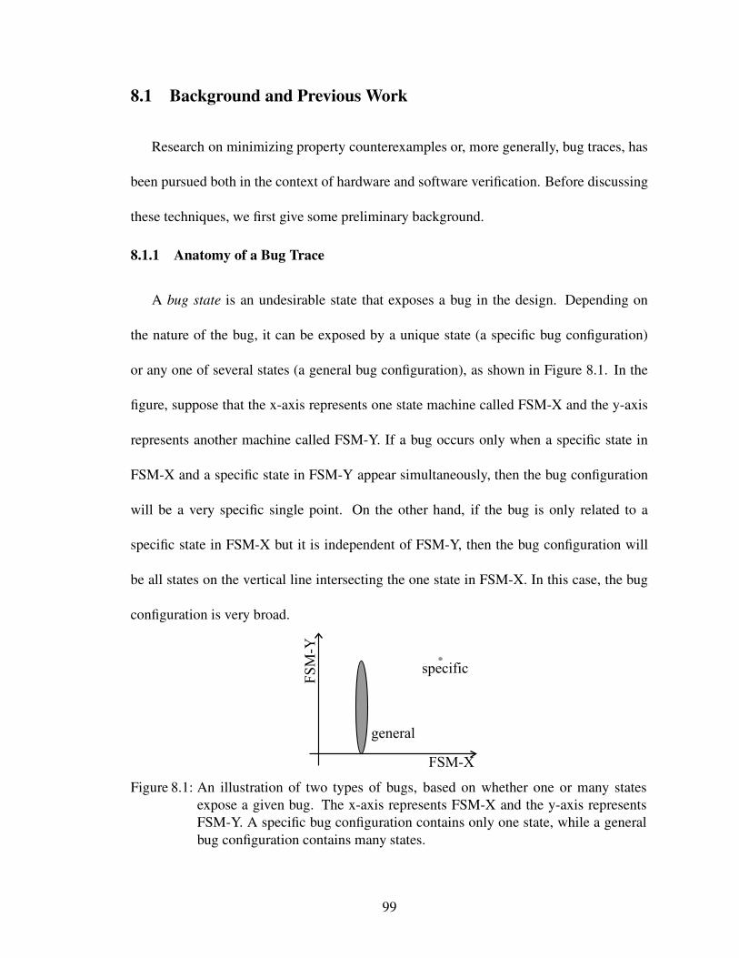
8.1 Background and Previous Work
Research on minimizing property counterexamples or, more generally, bug traces, has
been pursued both in the context of hardware and software verification. Before discussing
these techniques, we first give some preliminary background.
8.1.1 Anatomy of a Bug Trace
A bug state is an undesirable state that exposes a bug in the design. Depending on
the nature of the bug, it can be exposed by a unique state (a specific bug configuration)
or any one of several states (a general bug configuration), as shown in Figure 8.1. In the
figure, suppose that the x-axis represents one state machine called FSM-X and the y-axis
represents another machine called FSM-Y. If a bug occurs only when a specific state in
FSM-X and a specific state in FSM-Y appear simultaneously, then the bug configuration
will be a very specific single point. On the other hand, if the bug is only related to a
specific state in FSM-X but it is independent of FSM-Y, then the bug configuration will
be all states on the vertical line intersecting the one state in FSM-X. In this case, the bug
configuration is very broad.
Figure 8.1: An illustration of two types of bugs, based on whether one or many statesexpose a given bug. The x-axis represents FSM-X and the y-axis representsFSM-Y. A specific bug configuration contains only one state, while a generalbug configuration contains many states.
99
Given a sequential circuit and an initial state, a bug trace is a sequence of test vectors
that exposes a bug, i.e., causes the circuit to assume one of the bug states. The length of
the trace is the number of cycles from the initial state to the bug state, and an input event is
a change of an input signal at a specific clock cycle of the trace. One input event is consid-
ered to affect only a single input bit. An input variable assignment is a value assignment
to an input signal at a specific cycle. The term input variable assignment is used in the
literature when traces are modeled as sequences of symbolic variable assignments at the
design’s inputs. The number of input variable assignments in a trace is the product of the
number of cycles and the number of inputs. A checker signal is a signal used to detect a
violation of a property. In other words, if the signal changes to a specific value, then the
property monitored by the checker is violated, and a bug is found. The objective of bug
trace minimization is to reduce the number of input events and cycles in a trace, while still
detecting the checker violation.
Example 3 Consider a circuit with three inputs a, b and c, initially set to zero. Suppose
that a bug trace is available where a and c are assigned to 1 at cycle 1. At cycle 2, c
is changed to 0 and it is changed back to 1 at cycle 3, after which a checker detects a
violation. In this situation we count four input events, twelve input variable assignments,
and three cycles for our bug trace. The example trace is illustrated in Figure 8.2.
Another view of a bug trace is a path in the state space from the initial state to the bug
state, as shown in Figure 8.3. By construction, formal methods can often find the minimal
length bug trace as shown in the dotted line. Therefore we focus our minimization on
semi-formal and constrained-random traces only. However, if Butramin is applied to a
100

Figure 8.2: A bug trace example. The boxes represent input variable assignments to thecircuit at each cycle, shaded boxes represent input events. This trace has threecycles, four input events and twelve input variable assignments.
trace obtained with a formal technique, it may still be possible to reduce the number of
input events and variable assignments.
Figure 8.3: Another view of a bug trace. Three bug states are shown. Formal methodsoften find the minimal length bug trace, while semi-formal and constrained-random techniques often generate longer traces.
8.1.2 Known Techniques in Hardware Verification
Traditionally, a counterexample generated by BMC reports the input variable assign-
ments for each clock cycle and for each input of the design. However, it is possible, and
common, that only a portion of these assignments are required to falsify the property. Sev-
eral techniques that attempt to minimize the trace complexity have been recently proposed,
for instance, Ravi et al. [98]. To this end they propose two techniques: brute-force lifting
(BFL), which attempts to eliminate one variable assignment at a time, and an improved
variant that eliminates variables in such a way so as to highlight the primary events that
101

led to the property falsification. The basic idea of BFL is to consider the free variables of
the bug trace, that is, all input variable assignments in every cycle. For each free variable v,
BFL constructs a SAT instance SAT(v), to determine if v can prevent the counterexample.
If that is not the case, then v is irrelevant to the counterexample and can be eliminated.
Because this technique minimizes BMC-derived traces, its focus is only on reducing the
number of assignments to the circuit’s input signals. Moreover, each single assignment
elimination requires solving a distinct SAT problem, which may be computationally diffi-
cult. More recent work in [103] further improves the performance of BFL by attempting
the elimination of sets of variables simultaneously. Our technique for removing individual
variable assignments is similar to BFL as it seeks to remove an assignment by evaluating a
trace obtained with the opposite assignment. However, we apply this technique to longer
traces obtained with semi-formal methods and we perform testing via resimulation.
Another technique applied to model checking solutions is by Gastin et al. [55]. Here
the counterexample is converted to a Buchi automaton and a depth-first search algorithm
is used to find a minimal bug trace. Minimization of counterexamples is also addressed in
[66], where the distinction between control and data signals is exploited in attempting to
eliminate data signals first from the counterexample.
All of these techniques focus on reducing the number of input variable assignments to
disprove the property. Because the counterexample is obtained through a formal model
checker, the number of cycles in the bug trace is minimal by construction. Butramin’s ap-
proach considers a more general context where bug traces can be generated by simulation
or semi-formal verification software, attacking much more complex designs than BMC-
102

based techniques. Therefore, (1) traces are in general orders of magnitude longer than the
ones generated by BMC; and (2) there is much potential for reducing the trace in terms of
number of clock cycles, as our experimental results indicate. On the downside, the use of
simulation-based techniques does not guarantee that the results obtained are of minimal
length. As the experimental results in Section 8.5 indicate, however, our heuristics provide
in practice optimal results for most benchmarks.
Aside from minimization of bug traces generated using formal methods, techniques
that generate traces by random simulation have also been explored in the context of hard-
ware verification. One such technique is by Chen et al. [43] and proceeds in two phases.
The first phase identifies all the distinct states of the counterexample trace. The second
phase represents the trace as a state graph: it applies one step of forward state traversal
[48] to each of the individual states and adds transition edges to the graph based on it. Di-
jkstra’s shortest path algorithm is applied to the final graph obtained. This approach, while
very effective in minimizing the trace length (the number of clock cycles in the trace),
(1) does not consider elimination of input variable assignments, and (2) makes heavy use
of formal state-traversal techniques, which are notoriously expensive computationally and
can usually be applied only to small-size designs, as indicated also by the experimental
results in [43].
8.1.3 Techniques in Software Verification
The problem of trace minimization has been a focus of research also in the software
verification domain. Software bug traces are characterized by involving a very large num-
ber of variables and very long sequences of instructions. The delta debugging algorithm
103
[58] is fairly popular in the software world. It simplifies a complex software trace by ex-
tracting the portion of the trace that is relevant to exposing the bug. Their approach is
based exclusively on resimulation-based exploration and it attacks the problem by parti-
tioning the trace (which in this case is a sequence of instructions) and checking if any of
the components can still expose the bug. The algorithm was able to greatly reduce bug
traces in Mozilla, a popular web browser. A recent contribution that draws upon counter-
examples found by model checking is by Groce et al. [57]. Their solution focuses on
minimizing a trace with respect to the primitive constructs available in the language used
to describe the hardware or software system and on trying to highlight the causes of the
error in the counterexample, so as to produce a simplified trace that is more understandable
by a software designer.
8.2 Analysis of Bug Traces
In this section, we analyze the characteristics of bug traces generated using random
simulation, pointing out the origins of redundancy in these traces and propose how redun-
dancy can be removed. In general, redundancy exists because some portions of the bug
trace may be unrelated to the bug, there may be loops or shortcuts in the bug trace, or
there may be an alternative and shorter path to the bug. Two examples are given below to
illustrate the idea, while the following subsections provide a detailed analysis.
Example 4 Intel’s first-generation Pentium processor included a bug in the floating-point
unit which affected the FDIV instruction. This bug occurred when FDIV was used with a
specific set of operands. If there had been a checker testing for the correctness of the FDIV
operation during the simulation-based verification of the processor, it is very probable that
104

a bug trace exposing this problem may be many cycles long. However, only a small portion
of the random program would have been useful to expose the FDIV bug, while the majority
of other instructions can be eliminated. The redundancy of the bug trace comes from the
cycles spent testing other portions of the design, which are unrelated to the flawed unit
and can thus be removed.
Example 5 Suppose that the design under test is a FIFO unit, and a bug occurs every
time the FIFO is full. Also assume that there is a pseudo-random bug trace containing
both read and write operations until the trace reaches the “FIFO full” state. Obviously,
cycles that read data from the FIFO can be removed because they create state transitions
that bring the trace away from the bug configuration instead of closer to it.
8.2.1 Making Traces Shorter
In general, a trace can be made shorter if any of the following situations arise: (a) it
contains loops; (b) there are alternative paths (shortcuts) between two design states; or (c)
there is another state which exposes the same bug and can be reached earlier.
Figure 8.4: A bug trace may contain sequential loops, which can be eliminated to obtainan equivalent but more compact trace.
The first situation is depicted schematically in Figure 8.4. In random simulation, a
105

state may be visited more than once, and such repetitive states will form loops in the bug
trace. Identifying such loops and removing them can reduce the length of the bug trace.
Figure 8.5: Arrow 1 shows a shortcut between two states on the bug trace. Arrows marked“2” show paths to easier-to-reach bug states in the same bug configuration (thatviolates the same property).
In the second case, there may be a shortcut between two states as indicated by arrow 1
in Figure 8.5, which means an alternative path may exist from a state to another state using
fewer cycles. Such situations may arise in random traces frequently because constrained-
random simulation often selects transitions arbitrarily and it is possible that longer paths
are generated in place of shorter ones.
The third condition occurs when multiple design states exist that expose the same bug,
and some of them can be reached in fewer steps compared to the original one, as shown
by arrows marked “2” in Figure 8.5. If a path to those states can be found, it is possible to
replace the original one.
A heuristic approach that can be easily devised to search for alternative shorter traces
is based on generating perturbations on a given trace. A bug trace can be perturbed locally
or globally to find shortcuts or a path to an alternative bug state. In a local perturbation,
cycles or input events are added or removed from an original trace. As mentioned previ-
ously, random simulation selects state transitions in a pseudo-random fashion. By local
106

perturbation, alternative transitions can be explored and shorter paths to a trace state or
to another state exposing the bug may be found. In a global perturbation, a completely
new trace is generated, and the trace can be used to replace the original one if it is shorter.
One reason why perturbation has the potential to work effectively on random traces is that
a pseudo-random search tends to do a large amount of local exploration, compared to a
formal trace that progresses directly to a bug. Because of this, opportunities of shortcuts
within a trace abound.
8.2.2 Making Traces Simpler
After all redundant cycles are removed, many input events may still be left. For exam-
ple, if a circuit has 100 inputs and a bug trace is 100 cycles long, there are 10,000 input
variable assignments in the trace. However, not all assignments are relevant to expose the
bug. Moreover, redundant events increase the complexity of interpreting the trace in the
debugging phase. Therefore it is important to identify and remove such redundancy.
We envision two ways of simplifying the input assignments in a trace: by removing
input events and by eliminating assignments that are not essential to reach our goal. In this
latter approach, input assignments can be marked as essential or not, based on their impact
in exposing the bug. By removing nonessential input variable assignments, the analysis of
the bug trace during debugging can be made much simpler. For example, a trace with two
input events will be much easier to analyze than a trace with 10,000 input events.
107

8.3 Proposed Techniques
Based on our analysis, we propose several techniques to minimize a bug trace. In
this section we first provide an overview of these techniques, and then we discuss each
technique in detail.
1. Single-cycle elimination shortens a bug trace by resimulating a variant of the trace
which includes fewer simulation cycles.
2. Alternative path to bug is exploited by detecting when changes made on a trace
produce an alternative, shorter path to the bug.
3. State skip identifies all the unique state configurations in a trace. If the same state
occurs more than once, it indicates the presence of a loop between two states, and
the trace can be reduced.
4. BMC-based refinement attempts to further reduce the trace length by searching lo-
cally for shorter paths between two trace states.
In addition, we propose the following techniques to simplify traces:
1. Input-event elimination attempts to eliminate input events, by resimulating trace
variants which involve fewer input events.
2. Essential variable identification uses three-value simulation to distinguish essential
variable assignments from nonessential ones, and marks the nonessentials with “X”.
3. Indirectly, all cycle removal techniques may also remove redundant input events.
A bug trace can be perturbed by either adding or removing cycles or input events.
However, trying all possibilities is unfeasible. Since the purpose of minimization is to
108

reduce the number of cycles and input events, we only use removal in the hope to find
shorter and simpler traces. Our techniques are applied in the following order: Butramin
first tries to shorten a trace by removing certain clock cycles and simulating such trace
variants, after which it tries to reduce the number of input events. While analyzing each
perturbed trace, the two techniques of alternative path to bug and state skip monitor for
loops and shorter paths. Once these techniques run out of steam, Butramin applies a series
of BMC refinements. The BMC search is localized so that we never generate complex SAT
instances for SAT solving, which could become the bottleneck of Butramin. If our SAT
solver times out on some BMC instances, we simply ignore such instances and potential
trace reductions since we do not necessarily aim for the shortest traces.
8.3.1 Single-Cycle Elimination
Single-cycle elimination is an aggressive but efficient way to reduce the length and the
number of input events in a bug trace. It tentatively removes a whole cycle from the bug
trace and checks if the bug is still exposed by the new trace through resimulation, in which
case the new shorter trace replaces the old one. This procedure is applied iteratively on
each cycle in the trace, starting from cycle 1 and progressing to the end of the trace. The
reason we start from the first simulation cycle is that perturbing early stages of a trace has
a better chance to explore states far away from the original trace. The later a removal the
less the opportunity to visit states far away from the original trace.
Example 6 Consider the trace of Example 3. During the first step, single-cycle elimina-
tion attempts to remove cycle 1. If the new trace still exposes the bug, we obtain a shorter
bug trace which is only two cycles long and has two input events, as shown in Figure 8.6.
109

Note that it is possible that some input events become redundant because of cycle elimina-
tion, as it is the case in this example for the event on signal c at cycle 2. This is because
the previous transition on c was at cycle 1, which has now been removed. After events
which have become redundant are eliminated, single-cycle elimination can be applied to
cycle 2 and 3, iteratively.
Figure 8.6: Single-cycle elimination attempts to remove individual trace cycles, generat-ing reduced traces which still expose the bug. This example shows a reducedtrace where cycle 1 has been removed.
To reduce Butramin’s runtime, we extend single-cycle elimination to work with several
cycles at once. When three consecutive cycles are eliminated one by one, Butramin will
try to eliminate pairs of consecutive cycles. If that succeeds, the next attempt will consider
twice as many cycles. If it fails, the number of cycles considered at once will be halved.
This adaptive cycle elimination technique can dynamically extend its “window size” to
quickly eliminate large sequences of cycles when this is likely, but will roll back to single-
cycle removal otherwise.
Note that, when dependency exists between blocks of cycles, removing a single cycle
at a time may invalidate the bug trace. For example, removing any cycle within a PCI-
X transaction will almost always corrupt the transaction, rendering the bug trace useless.
This problem can be addressed by removing whole transactions instead of cycles. With
some extra inputs from the user to help identify transaction boundaries, Butramin can be
110

easily adapted to handle transaction-based traces.
8.3.2 Input-Event Elimination
Input-event elimination is the basic technique to remove input events from a trace.
It tentatively generates a variant trace where one input event is replaced by the comple-
mentary value assignment. If the variant trace still exposes the bug, the input event can
be removed. In addition, the event immediately following on the same signal becomes
redundant and can be removed as well.
Example 7 Consider once again the trace of Example 3. The result after elimination of
input event c at cycle 1 is shown in Figure 8.7. Note that the input event on signal c at
cycle 2 becomes redundant and it is also eliminated.
Figure 8.7: Input-event elimination removes pairs of events. In the example, the inputevents on signal c at cycle 1 and 2 are removed.
8.3.3 Alternative Path to Bug
An alternative path to bug occurs when a variant trace reaches a state that is different
from the final state of the trace, but it also exposes the same bug. The alternative state
must obviously be reached in fewer simulation steps than in the original trace. As shown
in Figure 8.8, if state s j2 , reached at time t2 by the variant trace (shown at the bottom)
exposes the bug, the new variant trace replaces the original one.
111

Figure 8.8: Alternative path to bug: the variant trace at the bottom hits the bug at step t2.The new trace replaces the old one, and simulation is stopped.
8.3.4 State Skip
The state skip rule is useful when two identical states exist in a bug trace. This happens
when there is a sequential loop in the trace or when, during the simulation of a tentative
variant trace, an alternative (and shorter) path to a state in the original trace is found.
Consider the example shown in Figure 8.9: if states s j2 and si4 are identical, then a new,
more compact trace can be generated by appending the portion from step t5 and on of
the original trace, to the prefix extracted from the variant trace up to and including step
t2. This technique identifies all reoccurring states in a trace and removes cycles between
them, guaranteeing that all the states in the final minimized trace are unique. States are
hashed for fast look-up so that state skip does not become a bottleneck in execution.
Figure 8.9: State skip: if state s j2 = si4 , cycles t3 and t4 can be removed, obtaining a newtrace which includes the sequence “... s j1 , s j2 , si5 , ...”.
112

8.3.5 Essential Variable Identification
We found that, after applying our minimization techniques, bug traces are usually
much shorter. However, many input variable assignments may still be part of the trace,
and their relevance in exposing the bug may vary – some may be essential, while others
are not. Butramin includes an “X-mode” feature for filtering out irrelevant input variable
assignments, where input variable assignments are classified as essential or not, based on
a 3-value (0/1/X) simulation analysis. To implement this technique, two bits are used to
encode each signal value, and each input assignment at each cycle is assigned in turn the
value X: if the X input propagates to the checker’s output and an X is sampled on the
checker’s output signal, then the input is marked essential, and the original input assign-
ment is kept. Otherwise, the input assignment is deemed irrelevant for the purpose of
exposing the bug. The set of input assignments that are marked irrelevant contribute to
simplify the debugging activity, since a verification engineer does not need to take them
into consideration when studying the cause of the system’s incorrect behavior. We present
experimental results indicating that this analysis is capable of providing substantial sim-
plifications to the signals involved in an already reduced bug trace.
Note, finally, that our simplification technique, which relies on 3-value simulation,
is over-conservative, flagging irrelevant input assignments as essential. Consider, for in-
stance, the simulation of a multiplexer where we propagated an X value to the select input
and a 1 value to both data inputs. A 3-valued logic simulator would generate X at the
output of the simulator; however, for our purposes, the correct value should have been 1,
since we consider X to mean “don’t-care”. If more accuracy is desired for this analysis, a
113

hybrid logic/symbolic simulator can be used instead [70, 117].
Alternatively, essential variable identification could be performed using a BMC-based
technique with a pseudo-Boolean SAT solver, for instance [51, 144]. Such solvers satisfy
a given SAT formula with the smallest possible number of assigned variables (maximal
number of don’t-cares). Aside from these solvers, even mainstream Boolean SAT solvers
can be specialized to do this, as suggested in [98]. Since assignments in the SAT solution
correspond to input variable assignments in the bug trace, those input variable assignments
are obviously essential. Essential variable identification naturally follows by marking all
other input variable assignments as irrelevant. A similar idea has been deployed also by
Lu et al. [82] to find a three-valued solution which minimizes the number of assignments
to state variables.
8.3.6 BMC-Based Refinement
This technique can be used after simulation-based minimization to further reduce the
length of a bug trace. Because of state skip, after applying simulation-based minimization,
no two states in a trace will be the same. However, shorter paths between any pair of states
may still exist. We propose here an approach based on model checking to find such paths.
The algorithm, also outlined in Figure 8.10, considers two states, say si and s j, which are k
1 Select two states si and s j , k cycles apart;2 for l = 1 to k−1 do3 C = circuit unrolled l times;4 Transform C into a Boolean formula CNFc;5 I=CNFc ∧CNFsi ∧CNFs j ;6 if (I is satisfiable)7 return (shortcut si → s j, l steps);
Figure 8.10: BMC-based shortcut detection algorithm.
114

cycles apart in the trace and attempts to find the shortest path connecting them. This path
can then be found by unrolling the circuit from 1 to k− 1 times, asserting si and s j as the
initial and final states, and attempting to satisfy the corresponding Boolean formula. If we
refer to the CNF formula of the unrolled circuit as CNFc, then CNFc∧CNFsi ∧CNFs j is the
Boolean formula to be satisfied. If a SAT solver can find a solution, then we have a shortcut
connecting si to s j. Note that the SAT instances generated by our algorithm are simplified
by the fact that CNFsi and CNFs j are equivalent to a partial satisfying assignment for the
instance. An example is given in Figure 8.11.
Figure 8.11: BMC-based refinement finds a shortcut between states S1 and S4, reducingthe overall trace length by one cycle.
The algorithm described in Figure 8.10 is applied iteratively on each pair of states that
are k steps apart in the bug trace, and using varying values for k from 2 to m, where m is
selected experimentally so that the SAT instance can be solved efficiently. We then build
an explicit directed graph using the shortcuts found by the BMC-based refinement and
construct the final shorter path from the initial state to the bug state. Figure 8.12 shows
an example of such graph. Each vertex in the graph represents a state in the starting trace,
edges between vertices represent the existence of a path between the corresponding states,
and the edge’s weight is the number of cycles needed to go from the source state to the
115

sink. Initially, there is an edge between each two consecutive vertices, and the weight
labels are 1. Edges are added between vertices when shortcuts are found between the
corresponding states, and they are labeled with the number of cycles used in the shortcut.
A single-source shortest path algorithm for directed acyclic graphs is then used to find
a shorter path from the initial to the bug state. While some of the shortcuts discovered
by BMC may be incompatible because of the partial constraints in CNFsi and CNFs j , the
algorithm we describe selects an optimal set of compatible shortcuts within the selected
window size m.
Although simulation-based techniques are effective, they are heuristic in nature and
may miss local optimization opportunities. BMC-based refinement has the potential to
improve on local optimizations by performing short-range optimal cycle elimination.
Figure 8.12: A shortest-path algorithm is used to find the shortest sequence from the initialstate to the bug state. The edges are labeled by the number of cycles neededto go from the source vertex to the sink. The shortest path from state 0 tostate 4 in the figure uses 2 cycles.
8.4 Implementation Insights
We built a prototype implementation of the techniques described in the previous sec-
tion to evaluate Butramin’s performance and trace reduction capability on a range of digital
designs. Our implementation strives to simplify a trace as much as possible, while pro-
viding good performance at the same time. This section discusses some of the insights we
gained while constructing a Butramin’s prototype.
116

8.4.1 System Architecture
The architecture of Butramin consists of three primary components: a driver program,
commercial logic simulation software, and a SAT solver. The driver program is respon-
sible for (1) reading the bug trace, (2) interfacing to the simulation tool and SAT solver
for the evaluation of the compressed variant traces, and (3) finding simplifications intro-
duced in the previous sections. The logic simulation software is responsible for simulating
test vectors from the driver program, notifying the system if the trace reaches the bug un-
der study, and communicating back to the driver each visited state during the simulation.
BMC-based minimization was implemented using MiniSat [51] that analyzes the SAT in-
stances generated by converting the unrolled circuits to CNF form using a CNF generator.
The system architecture is shown in Figure 8.13.
Figure 8.13: Butramin system architecture.
8.4.2 Algorithmic Analysis and Performance Optimizations
In the worst case scenario, the complexity of our simulation-based techniques is quadratic
in the length of the trace under evaluation, and linear in the size of the primary input sig-
117

nals of the design. In fact, consider an m-cycle long bug trace driving an n-input design.
The worst case complexity for our cycle-elimination technique is O(m2), where the one of
the input-event elimination technique is O(n×m2). All the other simulation-based tech-
niques have simpler complexity or are independent of the size of the trace or design. In
order to improve the runtime of Butramin, we developed an extra optimization as described
below. Experimental results show that the worst case situation did not occur due to our
optimization, adaptive cycle elimination and the nature of practical benchmarks.
The optimization focuses on identifying all multiple occurrences of a state so that we
can identify when the simulation of a variant trace falls into the original trace, and then
we can avoid simulating the last portion of the variant. To achieve this, we hash all states
visited by a trace and tag them with the clock cycle in which they occur. During the
simulation of variant traces we noted that, in some special conditions, we can improve
the performance of Butramin by reducing the simulation required: after the time when
the original and the variant traces differ, if a variant state matches a state in the original
trace tagged by the same clock cycle, then we can terminate the variant simulation and
still guarantee that the variant trace will hit the bug. In other words, simulation can be
terminated early because the result of applying the same test vectors after the matched
state will not change. We call this an early exit. As illustrated in Figure 8.14, early
exit points allow the simulation to terminate immediately. Often simulations can also be
terminated early by state skip optimization because the destination state is already in the
trace database. Experimental results show that this optimization is crucial to the efficiency
of simulation-based minimization techniques.
118

Figure 8.14: Early exit. If the current state s j2 matches a state si2 from the original trace,we can guarantee that the bug will eventually be hit. Therefore, simulationcan be terminated earlier.
8.4.3 Use Model
To run Butramin, the user must supply four inputs: (1) the design under test, (2) a bug
trace, (3) the property that was falsified by the trace, and (4) an optional set of constraints
on the design’s input signals. Traces are represented as Value Change Dump (VCD) files, a
common compact format that includes all top-level input events. Similarly, the minimized
bug traces are output as VCD files.
Removing input events from the bug trace during trace minimization may generate
illegal input sequences, which in turn could erroneously falsify a property or make the
trace useless. For example, removing the reset event from a bug trace may lead the design
into an erroneous state, generating a spurious trace which does not reflect a possible legal
activity of the design under verification, even if the simulation of such trace does expose
the original design flaw. Consequently, when testing sub-components of a design with
constrained inputs, it becomes necessary to validate the input sequences generated during
trace minimization. There are several ways to achieve this goal. One technique is to mark
required inputs so that Butramin does not attempt to remove the corresponding events from
the trace. This approach is a viable solution to handle, for instance, reset and the clock
119

signals. For complex sets of constraints, it is possible to convert them into an equivalent
circuit block connected to the original design, such as the techniques described in the work
by Yuan et al. [123]. This extra circuit block takes random input assignments and converts
them into a set of legal assignments which satisfy all the required environment constraints.
We deployed the former approach for simple situations, and we adapted the latter to the
context of our solution for benchmarks with more complex environments. Specifically,
since Butramin starts already with a valid input trace which it attempts to simplify, we
wrote our constraints as a set of monitors which observe each input sequence to the de-
sign. If the monitors flag an illegal transition during simulation, the entire “candidate
trace” is deemed invalid and removed from consideration. For BMC-based refinement,
these environmental constraints are synthesized and included as additional constraints to
the problem instance. Note, however, that this limits BMC-based techniques to be ap-
plied to designs whose environmental constraints are synthesizable. On the other hand,
this requirement is lifted for the simulation-based minimization techniques. From our ex-
perimental results, we observe that most minimization is contributed by simulation-based
techniques, which renders this requirement optional for most practical benchmarks.
We also developed an alternative use model to apply Butramin to reducing regression
runtime. In this context, the approach is slightly different since the goal now is to obtain
shorter traces that achieve the same functional coverage as their longer counterpart. To
support this, coverage points are encoded by properties: each of them is “violated” only
when the corresponding point is covered by the trace. Butramin can then be configured to
generate traces that violate all of the properties so that the same coverage is maintained.
120

8.5 Experimental Results
We evaluated Butramin by minimizing traces generated by a range of commercial ver-
ification tools: a constrained-random simulator, semi-formal verification software, and
again a semi-formal tool where we specified to use extra effort in generating compact
traces. We considered nine benchmark designs from OpenCores (FPU), ISCAS89 (S15850,
S38584), ITC99 (B15), IWLS2005 (VGALCD), picoJava (picoJava, ICU), as well as two
internally developed benchmarks (MULT, DES), whose characteristics are reported in Ta-
ble 8.1. We developed assertions to be falsified when not already available with the design,
and we inserted bugs in the design that falsify the assertions. Table 8.2 describes asser-
tions and bugs inserted. For ICU and picoJava, no bugs were injected but the constraints
for random simulation were relaxed. The checker for VGALCD is a correct duplicate
of the original design (which we modified to contain one design error), hence the circuit
size we worked with is twice as the one reported in Table 8.1. Finally, experiments were
conducted on a Sun Blade 1500 (1 GHz UltraSPARC IIIi) workstation running Solaris 9.
Table 8.1: Characteristics of benchmarks.Benchmark Inputs Flip-flops Gates DescriptionS38584 41 1426 20681 UnknownS15850 77 534 10306 UnknownMULT 257 1280 130164 Wallace tree multiplierDES 97 13248 49183 DES algorithmB15 38 449 8886 Portion of 80386FPU 72 761 7247 Floating point unitICU 30 62 506 PicoJava instruction cache unitpicoJava 53 14637 24773 PicoJava full designVGALCD 56 17505 106547 VGA/LCD controller
The benchmark setup for VGALCD involves duplicating this design and modifying one connectionin one of the copies. Butramin then minimizes the trace exposing the difference. It follows that thesize of the benchmark we work with is actually twice as the one reported for this design.
121

Table 8.2: Bugs injected and assertions for trace generation.Circuit Bug injected Assertion usedS38584 None Output signals forced to a specific valueS15850 None Output signals forced to a specific valueMULT AND gate changed with XOR Compute the correct output valueDES Complemented output Timing between receive valid, out-
put ready and transmit validB15 None Coverage of a partial design stateFPU divide on zero conditionally
complementedAssert divide on zero when divisor=0
ICU Constraints relaxed Buffer-full conditionpicoJava Constraints relaxed Assert SMU’s spill and fillVGALCD Circuit duplicated with one Outputs mismatch condition
wire changed in one copy
8.5.1 Simulation-Based Experiments
Our first set of experiments attempts to minimize traces generated by running a semi-
formal commercial verification tool with the checkers specified, and subsequently apply-
ing only the simulation-based minimization techniques of Butramin, described in Sections
8.3.1 to 8.3.4. We were not able to complete the generation of traces with the semi-formal
verification tool for VGALCD, therefore we only report results related to constrained-
random traces for this benchmark. Table 8.3 shows the absolute values of cycles and input
events left in each trace and the overall runtime of Butramin using only simulation-based
techniques. Figures 8.15 and 8.16 show the percentages of cycles and input events re-
moved from the original bug trace using different techniques. Note that for all benchmarks
we are able to remove the majority of cycles and input events.
With reference to Figure 8.15 and Figure 8.16, we observe that the contribution of
different minimization techniques varies among benchmarks. For example, almost all the
cycles and input events are removed by cycle elimination in FPU and picoJava. On the
122

Table 8.3: Cycles and input events removed by simulation-based techniques of Butraminon traces generated by semi-formal verification.
Circuit Cycles Input events RuntimeOriginal Remaining Removed Original Remaining Removed (seconds)
S38584 13 8 38.46% 255 2 99.22% 19S15850 59 1 98.31% 2300 3 99.87% 5MULT 345 4 98.84% 43843 2 99.99% 35DES 198 154 22.22% 3293 3 99.91% 254B15 25015 11 99.96% 450026 15 99.99% 57FPU 53711 5 99.99% 1756431 17 99.99% 27ICU 6994 3 99.96% 62740 3 99.99% 5picoJava 30016 10 99.97% 675485 11 99.99% 3359
other hand, state skip removes more than half of the cycles and input events in B15 and
ICU. This difference can be attributed to the nature of the benchmark: if there are fewer
state variables in the design, state skip is more likely to occur. In general, state skip has
more opportunities to provide trace reductions in designs that are control-heavy, such as
ICU, compared to designs that are datapath-heavy, such as FPU and picoJava. Although
input-event elimination does not remove cycles, it has great impact in eliminating input
events for some benchmarks, such as S38584. Overall, we found that all these techniques
are important to compact different types of bug traces.
Our second set of experiments applies Butramin to a new set of traces, also generated
by a semi-formal tool, but this time we configured the software to dedicate extra effort in
generating short traces, by allowing more time to be spent on the formal analysis of the
checker. Similar to Table 8.3 discussed earlier, Table 8.4 reports the results obtained by
applying the simulation-based minimization techniques of Butramin to these traces. We
still find that Butramin has a high impact in compacting these traces, even if, generally
speaking, they present less redundancy, since they are closer to be minimal. Note in par-
123

Figure 8.15: Percentage of cycles removed using different simulation-based techniques.For benchmarks like B15 and ICU, state skip is the most effective techniquebecause they contain small numbers of state variables and state repetition ismore likely to occur. For large benchmarks with long traces like FPU andpicoJava, cycle elimination is the most effective technique.
ticular, that the longer the traces, the greater the benefit from the application of Butramin.
Even if the overall impact is reduced, we still observe a 61% reduction in the number of
cycles and 91% in input events, on average.
Table 8.4: Cycles and input events removed by simulation-based techniques of Butraminon traces generated by a compact-mode semi-formal verification tool.
Circuit Cycles Input events RuntimeOriginal Remaining Removed Original Remaining Removed (seconds)
S38584 13 8 38.46% 255 2 99.22% 21S15850 17 1 94.12% 559 56 89.98% 4MULT 6 4 33.33% 660 2 99.70% 34DES 296 17 94.26% 3425 3 99.91% 17B15 27 11 59.26% 546 5 99.08% 6FPU 23 5 78.26% 800 17 97.88% 1ICU 19 14 26.32% 142 80 43.66% 1picoJava 26 10 61.54% 681 11 98.38% 39
The third set of experiments evaluated traces generated by constrained-random simu-
lation. Results are summarized in Table 8.5. As expected, Butramin produced the most
124

Figure 8.16: Number of input events eliminated with simulation-based techniques. Thedistributions are similar to cycle elimination because removing cycles alsoremoves input events. However, input-event elimination works the most ef-fectively for some benchmarks like S38584 and DES, showing that someredundant input events can only be removed by this technique.
impact on this set of traces, since they tend to include a large amount of redundant behav-
ior. The average reduction is 99% in terms of cycles and input events.
8.5.2 Performance Analysis
Table 8.6 compares Butramin’s runtime with and without different optimization tech-
niques. The traces are generated using semi-formal methods in this comparison. The exe-
cution runs that exceeded 40,000 seconds were timed-out (T/O in the table). The runtime
comparison shows that early exit and state skip have great impacts on the execution time:
early exit can stop resimulation early, and state skip may reduce the length of a trace by
many cycles at a time. Although these two techniques require extra memory, the reduction
in runtime shows they are worthwhile. In ICU, state skip occurred 4 times, removing 6977
cycles, which resulted in a very short runtime. The comparison also shows that adaptive
125

Table 8.5: Cycles and input events removed by simulation-based methods of Butramin ontraces generated by constrained-random simulation.
Circuit Cycles Input events RuntimeOriginal Remaining Removed Original Remaining Removed (seconds)
S38584 1003 8 99.20% 19047 2 99.99% 16S15850 2001 1 99.95% 77344 3 99.99% 2MULT 1003 4 99.60% 128199 2 99.99% 34DES 25196 154 99.39% 666098 3 99.99% 255B15 148510 10 99.99% 2675459 9 99.99% 395FPU 1046188 5 99.99% 36125365 17 99.99% 723ICU 31992 3 99.99% 287729 3 99.99% 5picoJava 99026 10 99.99% 2227599 16 99.99% 5125VGALCD 36595 4 99.99% 1554616 19 99.99% 28027
cycle elimination is capable of reducing minimization time significantly. This technique
is especially beneficial for long bug traces, such as FPU and picoJava.
A comparison of Butramin’s impact and runtime on the three sets of traces is summa-
rized in Figure 8.17. The result shows that Butramin can effectively reduce all three types
of bug traces in a reasonable amount of time. Note, in addition, that in some cases the
minimization of a trace generated by random simulation takes similar or less time than
applying Butramin to a trace generated by a compact-mode semi-formal tool, even if the
initial trace is much longer. That is the case for S38584 or S15850. We explain this effect
by the nature of the bug traces: traces generated by random simulation tend to visit states
that are easily reachable, therefore states are likely to be repetitive, and state skip occurs
more frequently, leading to a shorter minimization time. On the other hand, states visited
in a compact-mode generated trace are more frequently produced by formal engines and
can be highly specific, making state skip a rare event. The cases of FPU and picoJava
are relevant in this context: here state skips do not occur, and the minimization time is
highly related to the original trace length. They also demonstrate the benefits of Butramin
126

Table 8.6: Impact of the various simulation-based techniques on Butramin’s runtime.Benchmark Runtime(seconds)
[1]: cycle elimination+ [2]: [1]+state skip+ [3]: [2]+adaptiveinput-event elimination early exit cycle elimination
S38584 21 19 19S15850 11 5 5MULT 48 43 35DES 274 256 254B15 T/O 58 57FPU T/O 235 27ICU 8129 5 5
picoJava T/O T/O 3359Average 1697 66 64
Benchmarks that exceeded the time limit (40,000s) are not included in the average. Each of theruntime columns reports the runtime using only a subset of our techniques: the first cycle elimina-tion and input-event elimination. The second includes in addition early exit and state skip, and thethird adds also adaptive cycle elimination.
in various verification methodologies.
Figure 8.17: Comparison of Butramin’s impact when applied to traces generated in threedifferent modes. The graph shows the fraction of cycles and input eventseliminated and the average runtime.
8.5.3 Essential Variable Identification
We also applied the technique from Section 8.3.5 to identify essential variables from
the minimized traces we generated. Table 8.7 shows that after this technique is applied,
127

many input variable assignments are marked nonessential, further simplifying the trace.
Note that the comparison is now between input variable assignments, not input events.
Since all nonessential input variable assignments are simulated with X, the simulation
will propagate X values to many internal signals as well. As a result, it will be easier to
understand the impact of essential variable assignments on violated properties.
Table 8.7: Essential variable assignments identified in X-mode.Circuit Input variables Essential variablesS38584 320 2S15850 76 2MULT 1024 1019DES 14748 2B15 407 45FPU 355 94ICU 87 21picoJava 520 374
The table compares the number of input variable assignments in the minimized traces with thenumber of assignments classified essential. All the remaining assignments are nonessential andcan be replaced by X values in simulation. The initial traces were generated by a semi-formalverification tool.
8.5.4 Generation of High-Coverage Traces
In order to evaluate the effectiveness of Butramin on reducing regression runtime, we
selected three benchmarks, DES, FPU and VGALCD, as our multi-property benchmarks.
The original properties in the previous experiments were preserved, and the same traces
generated by constrained-random simulation were used. In addition, we included a few
extra properties, so that our original traces would expose them before reaching their last
simulation step, which still exposes the original property we used, as described in Table
2. Those extra properties specify a certain partial states to be visited or a certain output
signals to be asserted. Butramin is then configured to produce minimized traces that violate
128

Table 8.8: Cycles and input events removed by simulation-based methods of Butramin ontraces that violate multiple properties.
Circuit #Pro- Cycles Input events Runtimeperties Original Remaining Removed Original Remaining Removed (seconds)
DES 2 25196 184 99.27% 666098 17 99.99% 549FPU 3 1046188 9 99.99% 36125365 264 99.99% 580VGALCD 3 36595 5 99.98% 1554616 22 99.99% 25660
all properties. The results are summarized in Table 8.8. Compared with Table 8.5, it can
be observed that in order to cover extra properties, the length of the minimized traces
are now longer. However, Butramin continues to be effective for these multi-property
traces. We also found that the order of property violations is preserved before and after
minimization, suggesting that Butramin minimizes segments of bug traces individually.
From an algorithmic complexity point of view, minimizing a multi-property trace is similar
to minimizing many single-property traces with different initial states.
While the original traces of FPU and VGALCD require 20-30 minutes to be simulated,
post-Butramin traces are short enough to be simulated in just a few seconds. The benefits
of adding the minimized trace to a regression suite, instead of the original one, are obvious.
8.5.5 BMC-Based Experiments
We applied our BMC-based technique to traces already minimized by simulation-
based methods to evaluate the potential for further minimization. For VGALCD, we re-
port only data related to the minimization of random trace since semi-formal traces are
not available. The results are summarized in Table 8.9, where Orig is the original number
of cycles in the trace, and Removed is the number of cycles removed by this method. We
used a maximum window of 10 cycles (m = 10). The main observation that can be made is
that simulation-based techniques are very effective in minimizing bug traces. In fact, only
129

in two cases, ICU and B15, our BMC-based technique was able to extract additional min-
imization opportunities. Potentially, we could repeat the application of simulation-based
techniques and BMC-based methods until convergence, when no additional minimization
can be extracted.
Table 8.9: Cycles removed by the BMC-based method.Circuit Semi-formal Compact-trace Constrained-random
Orig Removed Time Orig Removed Time Orig Removed TimeS38584 8 0 55s 8 0 55s 8 0 55sS15850 1 0 2s 1 0 2s 1 0 2sMULT 4 0 20s 4 0 20s 4 0 20sDES 154 0 23h3m 17 0 357s 154 0 23h3mB15 11 1 121s 11 1 121s 10 0 97sFPU 5 0 5s 5 0 5s 5 0 5sICU 3 1 1s 14 2 1s 3 1 1spicoJava 10 0 70s 10 0 70s 10 0 104sVGALCD N/A N/A N/A N/A N/A N/A 4 0 985s
In order to compare the performance of the BMC-based technique with our simulation-
based methods, we applied the former directly, to minimize the original bug traces gen-
erated by semi-formal verification and by constrained-random simulation. For this ex-
periment, the time-out limit was set to 40,000 seconds. Results are summarized in Table
8.10, where benchmarks that timed-out are marked by “T/O”. The findings reported in
the table confirm that our BMC-based method should only be applied, if at all, after the
simulation-based techniques have already greatly reduced the trace complexity.
8.5.6 Evaluation of Experimental Results
We attempted to gain more insights into the experimental results by evaluating two
additional aspects of the minimized traces. We first checked how close the minimized
traces are to optimal-length traces such as those generated by formal verification. To do so,
130

Table 8.10: Analysis of a pure BMC-based minimization technique.Circuit Original Remained Runtime (s)S38584 13 9 403S15850 59 59 338MULT 345 T/O T/ODES 198 T/O T/OB15 25015 T/O T/OFPU 53711 T/O T/OICU 6994 700 856picoJava 30016 T/O T/OFPU 1046188 T/O T/OpicoJava 99026 T/O T/OVGALCD 36595 T/O T/O
This table shows the potential for minimizing traces using our BMC-based technique alone. Col-umn “Original” shows the length, in cycles of the original trace, and column “Remained” showsthe length of the minimized trace obtained after applying the BMC-based method. Traces in thetop-half were generated by semi-formal verification, and the ones in the bottom-half were gener-ated by constrained-random simulation. Experiments are timed-out at 40,000 seconds. The resultsof this table should be compared with Table 8.3 and 8.5.
we run full-fledged SAT-based BMC on our minimized traces. The results show that our
techniques found minimal-length bug traces for all benchmarks except DES (both traces
generated by random simulation and semi-formal verification). For those two traces, the
SAT solver ran out of memory after we unrolled the design by 118 cycles, and we could
not finish the experiment. No shorter traces were found between 1 and 118 cycles long.
We also tried to evaluate if the potential for simulation-based trace reduction was
mostly due to a large number of bug states, that is, a high number of design configura-
tions that expose a given bug (an example of this situation is provided in Figure 8.1). To
evaluate this aspect, we considered the original non-minimized traces in our experimen-
tal results. We first sampled the final state of the design after simulating the traces, and
then we fixed the goal of Butramin to generate a minimized trace that reaches that exact
same final state. The results of this experiment are summarized in Table 8.11. The table
131

shows that, for most benchmarks, the difference in the number of input events and cycles
removed is small, showing that the size of the bug configuration has a minimal impact on
the ability of Butramin to reduce and simplify a given bug trace, and our proposed solution
remains effective even when the bug configuration is very specific.
Table 8.11: Analysis of the impact of a bug radius on Butramin effectiveness.Circuit Cycles Input events
Original Same Same Original Same Sametrace bug state trace bug state
S38584 13 8 9 255 2 41S15850 59 1 1 2300 3 3MULT 345 4 4 43843 2 380DES 198 154 193 3293 3 1022B15 25015 11 11 450026 15 40FPU 53711 5 5 1756431 17 112ICU 6994 3 5 62740 3 6picoJava 30016 10 75 675485 11 1575FPU 1046188 5 6 36125365 17 120picoJava 99026 10 22 2227599 16 42VGALCD 36595 4 199 1554616 19 2068
The table compares number of cycles and input events in the original traces to the same valuesfrom minimized traces that hit the same bug, and to minimized traces that reach the same bugconfiguration. Traces in the top-half were generated by semi-formal software and traces in thebottom-half were generated by constrained-random simulation.
8.6 Summary
In this chapter we presented Butramin, a bug trace minimizer that combines simulation-
based techniques with formal methods. Butramin applies simple but powerful simulation-
based bug trace reductions, such as cycle elimination, input-event elimination, alternative
path to bug, state skip and essential variable identification. An additional BMC-based
refinement method is used after these techniques to exploit the potential for further mini-
mizations. Compared to purely formal methods, Butramin has the following advantages:
132

(1) it can reduce both the length of a bug trace and the number of its input events; (2)
it leverages fast logic-simulation engines for bug trace minimization and it can scale to
industrial size designs; and (3) it leverages existing simulation-based infrastructure, which
is currently prevalent in the industry. This significantly lowers the barriers for industrial
adoption of automatic design verification techniques.
Our experimental results show that Butramin can reduce a bug trace to just a small
fraction of its original length and complexity (estimated as the number of input events in
the trace) by using only simulation-based techniques. In fact, for most of the benchmarks
considered, we found that Butramin found an alternative trace of minimum length. In
addition we showed that these results are largely independent of the verification method-
ology used to generate the trace, whether based on simulation or semi-formal verification
techniques. The impact of Butramin appears to be uncorrelated with the size of the bug
configuration targeted by the trace, that is, the number of distinct design states that expose
the bug.
Recent follow-up work by Pan et al. [44] and Safarpour et al. [100] focuses on improv-
ing the formal analysis techniques for bug trace minimization, and their approaches can be
used to augment our BMC-based technique. As their experimental results suggest, how-
ever, formal analysis still cannot achieve the scalability provided by our simulation-based
minimization methods, making Butramin more suitable for practical designs.
133

CHAPTER IX
Functional Error Diagnosis and Correction
Recent improvements in design verification strive to automate the error-detection pro-
cess and greatly enhance engineers’ ability in detecting the presence of functional errors.
However, the process of diagnosing the cause of these errors and fixing them remains
difficult and requires significant manual effort. Our work proposes improvements to this
aspect of verification by presenting novel constructs and algorithms to automate the error-
repair process at both the gate level and the Register-Transfer Level (RTL). In this chapter,
we first extend the CoRe framework (see Chapter V) to handle sequential circuits. Next,
we present an innovative RTL error diagnosis and correction methodology. Finally, we
show the empirical evaluation of our functional error repair techniques and summarize
this chapter.
9.1 Gate-Level Error Repair for Sequential Circuits
The CoRe framework described in Chapter V only addresses the error-repair problem
for combinational circuits. CoRe is easily adaptable to correct errors in sequential circuits,
as described in this section. First of all, when operating on sequential circuits the user will
provide CoRe with input traces, instead of input patterns. A trace is a sequence of input
134

patterns, where a new pattern is applied to the design’s inputs at each simulation cycle, and
the trace can be either error-sensitizing or functionality-preserving. To address sequential
circuits, we adopt the diagnosis techniques from Ali et al. [6] relating to sequential cir-
cuits. The idea is to first unroll the circuit by connecting the outputs of the state registers
to the inputs of the registers in the previous cycle, and then use the test vectors to constrain
the unrolled circuit. Given an initial state and a set of test vectors with corresponding
correct output responses, Ali’s error-diagnosis technique is able to produce a collection of
error sites, along with their correct values, that rectify the incorrect output responses.
To correct errors in sequential designs we apply the same algorithm described in Sec-
tion 5.2.1 with two changes: the diagnosis procedure should be as described in [6], and
the signature generation function is modified so that it can be used in a sequential design.
Specifically, the new sequential signature generation procedure should record one bit of
signature for each cycle of each sequential trace that we simulate. For instance, if we have
two traces available, a 4-cycle trace and a 3-cycle trace, we will obtain a 7-bit signature
at each internal circuit node. An example of the modified signature is shown in Figure
9.1. In our current implementation, we only use combinational Observability Don’t-Cares
(ODCs). In other words, we still treat inputs of state registers as primary outputs when
calculating ODCs. Although it is possible to exploit sequential ODCs for resynthesis, we
do not pursue this optimization, yet.
Trace1 Trace2Cycle 1 2 3 4 1 2 3Signature 0 1 1 0 1 0 1
Figure 9.1: Sequential signature construction example. The signature of a node is built byconcatenating the simulated values of each cycle for all the bug traces. In thisexample, trace1 is 4 cycles and trace2 is 3 cycles long. The final signature isthen 0110101.
135
9.2 Register-Transfer-Level Error Repair
To develop a scalable and powerful RTL error diagnosis and correction system, we
extend our gate-level techniques to the RTL. This approach is significantly more accurate
than previous software-based RTL solutions [64, 96, 104] (see Section 2.1) in that we can
analyze designs rigorously using formal hardware verification techniques. At the same
time, it is considerably faster and more scalable than gate-level diagnosis because errors
are modeled at a higher level. Moreover, it only requires test vectors and output responses,
making it more practical than existing formal analysis solutions [16]. Finally, the novel
error model and increased accuracy of our approach allow our technique to provide in-
sightful suggestions for correcting diagnosed errors. Our main contributions include: (1) a
new RTL error model that explicitly inserts MUXes into RTL code for error diagnosis, as
opposed to previous solutions that use MUXes implicitly; (2) innovative error-diagnosis
algorithms using synthesis or symbolic simulation; and (3) a novel error-correction tech-
nique using signal behaviors (signatures) that are especially suitable for the RTL. Our
empirical results show that these techniques allow us to provide highly accurate diagnoses
very quickly.
We implemented our techniques in a framework called REDIR (RTL Error DIagnosis
and Repair), highlighted in Figure 9.2. The inputs to the framework include a design con-
taining one or more bugs, a set of test vectors exposing them, and the correct responses for
the primary outputs over the given test vectors (usually generated by a high-level behav-
ioral model written in C, C++, SystemC, etc.). Note that we only require the correct re-
sponses at the primary outputs of the high-level model and no internal values are required.
136

!! "#$$$%
&'(
#
"#
"#
"
)
*(
"
"## ##+
,-
%
)
" +
Figure 9.2: REDIR framework. Inputs to the tool are an RTL design (which includes oneor more errors), test vectors exposing the bug(s), and correct output responsesfor those vectors obtained from a high-level simulation. Outputs of the tool in-clude REDIR symptom core (a minimum cardinality set of RTL signals whichneed to be modified in order to correct the design), as well as suggestions tofix the errors.
The output of the framework is a minimum cardinality set of RTL signals that should be
corrected in order to eliminate the erroneous behavior. We call this set the symptom core.
When multiple cores exist, REDIR provides all of the possible minimal cardinality sets.
In addition, the framework suggests several possible fixes of the signals in the symptom
core to help a designer correct those signals.
The rest of the section is organized as follows. In Section 9.2.1, we provide the nec-
essary background. Section 9.2.2 describes our error-diagnosis techniques, while Section
9.2.3 explains our error-correction method.
9.2.1 Background
Our error-diagnosis algorithm converts the error-diagnosis problem into a Pseudo-
Boolean (PB) problem, and then uses a PB solver to perform the diagnosis and infer which
137

design signals are responsible for incorrect output behavior. In this subsection, we first de-
fine Pseudo-Boolean problems, which are an extension of SATisifiability problems. Next,
we review the basic idea behind symbolic simulation, which we use as an alternative,
compact way to formulate the PB problem.
Pseudo-Boolean Problems
PB problems, also called 0-1 integer linear programming problems, are an extension of
SATisfiability problems. A Pseudo-Boolean Constraint (PBC) is specified as an inequality
with a linear combination of Boolean variables: C0 po +C1 p1 + ...+Cn−1 pn−1 ≥Cn, where
the variables pi are defined over the Boolean set 0, 1. A PB problem allows the use of
an additional objective function, which is a linear expression that should be minimized
or maximized under the given constraints. A number of PB solvers have been developed
recently by extending existing SAT solvers (for instance, MiniSat+ [52]).
Logic vs. Symbolic Simulation
Logic simulation models the behavior of a digital circuit by propagating scalar Boolean
values (0 and 1) from primary inputs to primary outputs. For example, when simulating 2-
input AND with both inputs set to 1, the output 1 is produced. On the other hand, symbolic
simulation uses symbols instead of scalar values and produces Boolean expressions at the
outputs [14, 19]. As a result, simulating a 2-input XOR with inputs a and b generates an
expression “a XOR b” instead of a scalar value. To improve scalability, modern symbolic
simulators employ several techniques, including approximation, parameterization and on-
the-fly logic simplification [13]. For example, with on-the-fly logic simplification, “0 XOR
b” is simplified to b thus reducing the complexity of the expression. Traditional symbolic
138

simulators operate on a gate-level model of a design; however, in recent years simulators
operating on RTL descriptions have been proposed [70, 71]. Symbolic simulation is an
alternative way to generate an instance of the PB constraint problem that we use in our
error-diagnosis framework.
9.2.2 RTL Error Diagnosis
In this subsection, we describe our error-diagnosis techniques. First, we explain our
RTL error model, and then propose two diagnosis methods that use either synthesis or
symbolic simulation. Finally, we outline how hierarchical designs should be handled.
Error Modeling
In our framework the error-diagnosis problem is represented with (1) an RTL descrip-
tion containing one or more bugs that is composed of variables (wires, registers, I/O) and
operations on those variables; (2) a set of test vectors exposing the bugs; and (3) the correct
output responses for the given test vectors, usually generated by a high-level behavioral
model. The objective of the error diagnosis is to identify a minimal number of variables
in the RTL description that are responsible for the design’s erroneous behavior. Moreover,
by modifying the logic of those variables, the design errors can be corrected. Each signal
found to affect the correctness of the design is called a symptom variable. Without min-
imization, the set of symptom variables reported would include the root cause of the bug
and the cone of logic emanating from it: correcting all the symptom variables on any cut
across this cone of logic would eliminate the bug. Therefore, by forcing the PB solver to
minimize the number of symptom variables, we return a solution as close to the root cause
of the erroneous behavior as possible.
139

To model errors in a design, we introduce a conditional assignment for each RTL
variable, as shown in the example in Figure 9.3. Note that these conditional assignments
are used for error diagnosis only and should not appear in the final synthesized design.
However, they allow the REDIR framework to locate sites of erroneous behavior in RTL,
as we illustrate using a half adder design shown in Figure 9.3. Suppose that the output
responses of the design are incorrect because c should be driven by “a & b” instead of “a
| b”. Obviously, to produce the correct output that we obtain from a high-level model, the
behavior of c must be changed. To model this situation, we insert a conditional assignment,
“assign cn = csel ? c f : c”, into the code. Next, we replace all occurrences of c in the code
with cn, except when c is used on the left-hand-side of an assignment. We call csel a select
variable and c f a free variable. Then, by asserting csel and using an alternative signal
source, modeled by c f , we can force the circuit to behave as desired. If we can identify
the select variables that should be asserted and the correct signals that should drive the
corresponding free variables to produce correct circuit behavior, we can diagnose and fix
the errors in the design.
The procedure to introduce a conditional assignment for a design variable v is called
MUX-enrichment (since conditional assignments are conceptually multiplexers), and its
pseudo-code is shown in Figure 9.4. It should be performed on each internal signal, defined
in the circuit, including registers. The primary inputs, however, should not be MUX-
enriched since by construction they cannot have erroneous values. It also should be noted
that for hierarchical designs the primary inputs of a module may be driven by the outputs
of another module and, therefore, may assume erroneous values. To handle this situation,
140

module half adder(a, b, s, c);input a, b;output s, c;assign s = a ˆ b;assign c = a | b;
endmodulemodule half adder MUX enriched(a, b, sn, cn, ssel , csel , s f , c f );input a, b, ssel , csel , s f , c f ;output sn, cn;assign s = a ˆ b;assign c = a | b;assign sn = ssel ? s f : s;assign cn = csel ? c f : c;
endmoduleFigure 9.3: An RTL error-modeling code example: module half adder shows the original
code, where c is erroneously driven by “a | b” instead of “a & b”; and modulehalf adder MUX enriched shows the MUX-enriched version. The differencesare marked in boldface.
procedure MUX enrichment(v)1. create a new signal wire vn and new inputs v f and vsel ;2. add conditional assignment “vn = vsel ? v f : v”;3. replace all occurrences of v that appear on the right-hand-side of
assignments (including outputs, if/case conditions, etc.) with vn;Figure 9.4: Procedure to insert a conditional assignment for a signal in an RTL description
for error modeling.
we insert conditional assignments into the hierarchical modules’ output ports.
Diagnosis with Synthesis
After the error-modeling constructs have been inserted into a design, error diagnosis
is used to identify the minimal number of select variables that should be asserted along
with the values of their corresponding free variables to produce the correct circuit behav-
ior. In this section we present an error-diagnosis technique that uses synthesis and circuit
unrolling. In contrast with existing gate-level diagnosis techniques described in Section
5.1.3, our RTL error-modeling constructs are synthesized with the design, which elimi-
141

nates the need to insert multiplexers at the gate level. In this way, the synthesized netlist
faithfully preserves the constructs inserted at the RTL, enabling accurate RTL error diag-
nosis. This is significantly different from diagnosing design errors at the gate level, since
synthesis is only used to generate Boolean expressions between RTL variables, and the
synthesized netlist is not the target of the diagnosis. As a result, our diagnosis method has
a much smaller search space and runs significantly faster than gate-level techniques, as we
show in our experimental results.
Procedure syn based diagnosis(designCNF,c, inputs,out puts)1 CNF = unroll designCNF c times;2 connect all select variables in CNF to those in the first cycle;3 constrain PI/PO in CNF using inputs/out puts;4 PBC = CNF, min( ∑ select variables);5 return solution= PB-Solve(BPC);
Figure 9.5: Procedure to perform error diagnosis using synthesis and circuit unrolling.
Figure 9.5 outlines the algorithm for synthesis-based error diagnosis. Before the proce-
dure is called, the design is synthesized and its combinational portion is converted to CNF
format (designCNF). Other inputs to the procedure include the length of the bug trace, c,
as well as the test vectors (inputs) and their correct output responses (out puts). To make
sure that the diagnosis applies to all simulation cycles, the algorithm connects the select
variables for each unrolled copy to the corresponding CNF variables in the first copy. On
the other hand, free variables for each unrolled copy of the circuit are independent. When
a solution is found, each asserted select variable is a symptom variable, and the solution
for its corresponding free variable is an alternative signal source that can fix the design er-
rors. Note that if state values over time are known, they can be used to constrain the CNF
at register boundaries, reducing the sequential error-diagnosis problem to combinational.
142

The constructed CNF, along with the objective to minimize the sum of select variables,
forms a PBC. Error diagnosis is then performed by solving the PBC.
Diagnosis with RTL Symbolic Simulation
Here we propose an alternative error-diagnosis technique that scales further than the
synthesis-based technique. We achieve this by performing symbolic simulation directly
on the RTL representation and generating Boolean expressions at the primary outputs for
all simulated cycles. The outputs’ Boolean expressions are used to build a PB problem’s
instance, that is then handed over to a PB solver for error diagnosis.
Although RTL symbolic simulators are not yet commonly available in the industry,
effective solutions have been proposed recently in the literature [70, 71]. Moreover, be-
cause of the scalability advantages of performing symbolic simulation at the RTL instead
of the gate level, commercial-quality solutions are starting to appear. For our empirical
validation we used one such experimental RTL symbolic simulator [126].
Figure 9.6 illustrates our novel procedure that uses symbolic simulation and PB solv-
ing. We assume that the registers are initialized to known values before the procedure
is invoked. We also assume that the circuit contains n MUX-enriched signals named vi,
where i = 1..n. Each vi has a corresponding select variable vi sel and a free variable
vi f . There are o primary outputs, named PO j, where j = 1..o. We use subscript “@”
to prefix the cycle during which the symbols are generated. For each primary output j
and for each cycle t we compute expression PO j@t by symbolically simulating the given
RTL design, and also obtain correct output value CPO j@t from the high-level model. The
inputs to the procedure are the RTL design (design), the test vectors (test vectors), and the
143

Procedure sim based diagnosis(design, test vectors,CPO)1 ∀i,1 ≤ i ≤ n, vi sel= new symbol();2 for t = 1 to c begin // Simulate c cycles3 PI = test vector at cycle t;4 ∀i,1 ≤ i ≤ n, vi f @t= new symbol();5 PO@t = simulate(design);6 end7 PBC =
Voj=1
Vct=1(PO j@t== CPO j@t), min(∑n
i=1vi sel);8 return solution= PB Solve(PBC);
Figure 9.6: Procedure to perform error diagnosis using symbolic simulation. The bold-faced variables are symbolic variables or expressions, while all others arescalar values.
correct output responses over time (CPO).
In the algorithm shown in Figure 9.6, a symbol is initially created for each select vari-
able (line 1). During the simulation, a new symbol is created for each free variable in every
cycle, and test vectors are applied to primary inputs, as shown in lines 2-4. The reason for
creating only one symbol for each select variable is that a conditional assignment should
be either activated or inactivated throughout the entire simulation, while each free variable
requires a new symbol at every cycle because the value of the variable may change. As a
result, the symbols for the select variables are assigned outside the simulation loop, while
the symbols for the free variables are assigned in the loop. The values of the free variables
can be used as the alternative signal source to produce the correct behavior of the circuit.
After simulating one cycle, a Boolean expression for all of the primary outputs are created
and saved in PO@t (line 5). After the simulation completes, the generated Boolean expres-
sions for all the primary outputs are constrained by their respective correct output values
and are ANDed to form a PBC problem as line 7 shows. In order to minimize the number
of symptom variables, we minimize the sum of select variables, which is also added to the
PBC as the objective function. A PB solver is then invoked to solve the formulated PBC,
144

as shown in line 8. In the solution, the asserted select variables represent the symptom
variables, and the values of the free variables represent the alternative signal sources that
can be used to correct the erroneous output responses.
Below we present an example of a buggy design to illustrate the symbolic simulation-
based error-diagnosis technique.
module example(clk, I1, I2, O1n, O2n, g1sel , O1sel , O2sel , g1 f , O1 f , O2 f );input I1, I2, g1sel , O1sel , O2sel , g1 f , O1 f , O2 foutput O1n, O2n;reg r1, r2;initial begin r1= 0; r2= 0; endalways @(posedge clk) beginr1= I1; r2= I2;
endassign g1 = r1 — r2;assign O1 = I1 — g1n;assign O2 = I2 & g1n;assign g1n= g1sel ? g1 f : g1;assign O1n= O1sel ? O1 f : O1;assign O2n= O2sel ? O2 f : O2;
endmoduleFigure 9.7: Design for the example. Wire g1 should be driven by “r1 & r2”, but it is
erroneously driven by “r1 | r2”. The changes made during MUX-enrichmentare marked in boldface.
Example 8 Assume that the circuit shown in Figure 9.7 contains an error: signal g1 is
erroneously assigned to expression “r1 | r2” instead of “r1 & r2”. Conditional assign-
ments, highlighted in boldface, have been inserted into the circuit using the techniques
described in Section 9.2.2. For simplicity reasons, we do not include the MUXes at the
outputs of registers r1 and r2. The trace that exposes the error in two simulation cycles
consists of the following values for inputs I1, I2: 0, 1, 1, 1. When the same trace is
simulated by a high-level behavioral model, the correct output responses for O1, O2 are
generated: 0, 0, 1, 0. Besides these output responses, no addition information, such
145

as values of internal signals and registers, is required. We annotate the symbols injected
during the simulation by their cycle numbers using subscripts. The Boolean expressions
for the primary outputs for the two cycles of simulation are:
O1n@1= O1sel ? O1 f @1 : [I1@1 | (g1sel ? g1 f @1 : 0)]
O2n@1= O2sel ? O2 f @1 : [I2@1 & (g1sel ? g1 f @1 : 0)]
O1n@2= O1sel ? O1 f @2 : I1@2 | [g1sel ? g1 f @2 : (I1@1 & I2@1)]
O2n@2= O2sel ? O2 f @2 : I2@2& [g1sel ? g1 f @2 : (I1@1 & I2@1)]
Since the primary inputs are scalar values, the expressions can be greatly simplified dur-
ing symbolic simulation. For example, we know that I1@2=1; therefore, O1n@2 can be
simplified to O1sel ? O1 f @2 : 1. As a result, the Boolean expressions actually generated
by the symbolic simulator are:
O1n@1= O1sel ? O1 f @1 : (g1sel ? g1 f @1 : 0)
O2n@1= O2sel ? O2 f @1 : (g1sel ? g1 f @1 : 0)
O1n@2= O1sel ? O1 f @2 : 1
O2n@2= O2sel ? O2 f @2 : (g1sel ? g1 f @2 : 0)
To perform error diagnosis, we constrain the output expressions using the correct re-
sponses, and then construct a PBC as follows:
PBC = (O1n@1 == 0)∧ (O2n@1 == 0)∧ (O1n@2 == 1)∧ (O2n@2 == 0),
min(O1sel + O2sel + g1sel ).
One solution of this PBC is to assert g1sel , which provides a correct symptom core.
146

Handling Hierarchical Designs
Current designs often have hierarchical structures to allow the circuits to be decom-
posed into smaller blocks and thus reduce their complexity. Here we discuss how a MUX-
enriched circuit should be instantiated if it is encapsulated as a module in such a hierarchi-
cal design.
The algorithm to insert MUXes into a single module m is shown in Figure 9.4. If m is
instantiated inside of another module M, however, MUX-enrichment of M must include an
extra step where new inputs are added to all instantiations of m. Therefore, for hierarchical
designs, the insertion of conditional assignments must be performed bottom-up: MUX-
enrichment in a module must be executed before it is instantiated by another module.
This is achieved by analyzing the design hierarchy and performing MUX-enrichment in a
reverse-topological order.
It is important to note that in hierarchical designs, the select variables of instances of
the same module should be shared, while the free variables should not. This is because all
instances of the same module will have the same symptom variables. As a result, select
variables should share the same signals. On the other hand, each instance is allowed to
have different values for their internal signals; therefore, each free variable should have its
own signal. However, it is possible that a bug requires fixing only one RTL instance while
other instances of the same module can be left intact. This situation requires generation of
new RTL modules and is currently not handled by our diagnosis techniques.
147

9.2.3 RTL Error Correction
The RTL error-correction problem is formulated as follows: given an erroneous RTL
description of a digital design, find a variant description for one or more of the modules
that compose it so that the new design presents a correct behavior for the errors, while
leaving the known-correct behavior unchanged. Although many error-repair techniques
exist for gate-level designs, very few studies focus on the RTL. One major reason is the
lack of logic representations that can support the logic manipulation required during RTL
error correction. For example, the logic of a signal in a gate-level netlist can be easily
represented by BDDs, and modifying the function of the signal can be supported by the
manipulation of its BDDs. However, most existing logic representations cannot be easily
applied to an RTL variable. This problem is further exacerbated by the fact that an RTL
module may be instantiated multiple times, creating many different functions for an RTL
variable depending on where it is instantiated.
In this subsection, we first describe the baseline error-correction technique that is easier
to understand. Next, we show how signatures should be generated at the RTL to handle
hierarchical and sequential designs. Finally, we provide some insights that we obtained
during the implementation of our system.
Baseline Error Correction Technique
For a flattened combinational design, error correction is performed as follows: (1) sig-
natures of RTL variables are generated using simulation; (2) error diagnosis is performed
to find a symptom core; (3) signatures of the symptom variables in the symptom core are
replaced by the values of their corresponding free variables; and (4) synthesis is applied
148

to find logic expressions generating the signatures of the symptom variables. By replac-
ing the expressions that generate the functions of the symptom variables with those new
expressions, design errors can be corrected.
Hierarchical and Sequential Designs
In a flattened design, each RTL variable represents exactly one logic function. In a
hierarchical design, however, each variable may represent more than one logic function.
Therefore, we devise the following techniques to construct the signatures of RTL variables.
For clarity, we call a variable in an RTL module a module variable and a variable in an
instance generated by the module an instance variable. A module variable may generate
multiple instance variables if the module is instantiated several times.
In RTL error correction, we modify the source code of the modules in order to correct
the design’s behavior. Since changing an RTL module will affect all the instances produced
by the module, we concatenate the simulation values of the instance variables derived from
the same module variable to produce the signature for the module variable. This way, we
can guarantee that a change in a module will affect instances in the same way. Similarly,
we concatenate the signatures of the module variable at different cycles for sequential error
correction. A signature-construction example is given in Figure 9.8. Note that to ensure
the correctness of error repair, the same instance and cycle orders must be used during the
concatenation of signatures for all module variables.
Example 9 Using the same circuit as Example 8. The values returned by the PB solver
for g1 f @0 and g1 f @1 are both 0. Since the inputs to g1 are 0, 0 and 0, 1 for the first
two cycles, the correct expression for g1 should generate 0 for these two inputs. RTL error
149

Design:module top;
child c1(), c2(), c3();
endmodule
module child;
wire v;
endmodule
Simulation values:Cycle 0: top.c1.v = 0, top.c2.v = 0, top.c3.v = 1Cycle 1: top.c1.v = 1, top.c2.v = 0, top.c3.v = 0
Constructed signature for RTL error correction:
child.v =c1.v︷︸︸︷
1c2.v︷︸︸︷
0c3.v︷︸︸︷
0︸ ︷︷ ︸
cycle 1
c1.v︷︸︸︷
0c2.v︷︸︸︷
0c3.v︷︸︸︷
1︸ ︷︷ ︸
cycle 0
Figure 9.8: Signature-construction example. Simulation values of variables created fromthe same RTL variable at all cycles should be concatenated for error correction.
correction returns the following new logic expressions that can fix the error: g1 = r1&r2,
g1 = r1, etc. Note that although the correct fix is returned, the fix is not unique. In general,
longer traces containing various test vectors will identify the error with higher precision
and suggest better fixes than short ones.
Identifying Erroneous Code Statements
Several existing error-diagnosis techniques are able to identify the RTL code state-
ments that may be responsible for the design errors [65, 96, 104, 109]. Unlike these
techniques, REDIR returns the RTL variables that are responsible for the errors instead.
Since one variable may be affected by multiple statements, the search space of the errors
modeled by these techniques tend to be larger than REDIR, making REDIR more efficient
in error diagnosis. On the other hand, being able to identify erroneous statements may
further localize the errors and make debugging easier. To achieve this goal, we observe
that in correctly designed RTL code, the value of a variable should be affected by at most
150

one statement at each cycle. Otherwise, a multiple-driven error will exist in the design.
Based on this observation, we develop the following procedure to identify the erroneous
code statements using our error-diagnosis results.
Given a symptom variable, we first record the cycles at which the values of its free
variables are different from its simulated values. Next, we identify the code statements
that assign new values to the symptom variable for those cycles: these code statements
are responsible for the errors. Since many modern logic simulators provide the capability
to identify the executed code statements (e.g., full-trace mode in Cadence Verilog-XL),
erroneous statements can be pinpointed easily by replaying the bug traces used for error
diagnosis. After erroneous statements are identified, signatures for error-correction can be
generated using only the cycles when the statements are executed. In this way, we can
produce corrections specifically for the erroneous statements.
Implementation Insights
When multiple bug traces are used in the diagnosis, the set of the reported symptom
variables is the intersection of the symptoms identified by each bug trace. Therefore, to
accelerate the diagnosis over a specific bug trace, we can deassert the select variables that
are never asserted during the execution of previous traces.
Fixing errors involving multi-bit variables is more difficult than fixing errors involv-
ing only one-bit variables because different bits in the variable may be generated differ-
ently. To solve this problem, we allow the user to insert a conditional assignment for
each bit in the variable. Alternatively, REDIR can also be configured to consider only the
least-significant bit when performing error correction. This is useful when the variable is
151

considered as a whole.
In synthesis-based error diagnosis, we observe that it is difficult to identify the wires
derived from the same RTL variable in a synthesized netlist. To overcome this problem,
we add the outputs of inserted conditional statements to the primary outputs of the MUX-
enriched modules to obtain the simulated values of the RTL variables. To improve our
error-correction quality, we utilize ODCs in our synthesis-based approach by simulating
the complement signatures of symptom variables and observe the changes at primary out-
puts (including inputs to registers).
9.3 Experimental Results
In this section we present experimental results of our error-repair techniques at both
the gate level and the RTL. At the gate level, we first evaluate the effectiveness of the
baseline CoRe framework on fixing bugs in combinational designs. Next, we use the
extension described in Section 9.1 to repair errors in sequential designs. At the RTL, we
first evaluate our error-diagnosis techniques and contrast the results with those at the gate
level. We then show the results on automatic error correction.
9.3.1 Gate-Level Error Repair
We implemented our CoRe framework using the OAGear package [140] because it pro-
vides convenient logic representations for circuits. We adopted Smith’s [107] algorithm
and integrated MiniSat [51] into our system for error diagnosis and equivalence checking.
We used Espresso [99] to optimize the truth table returned by DPS, and then we con-
structed the resynthesized netlist using AND, OR and INVERTER gates. Our testcases
152

were selected from IWLS2005 benchmarks [138] based on designs from ISCAS89 and
OpenCores suites. In our implementation, we limited the number of attempts to resynthe-
size a wire to 30, and we prioritized our correction by starting from fixes with wires closer
to primary inputs. We conducted four experiments on a 2.0GHz Pentium 4 workstation.
The first two experiments are in the context of equivalence checking, the third one deals
with simulation-based verification, while the last one repairs errors in sequential circuits.
Equivalence checking: our first experiment employs Application 1 described in Sec-
tion 5.2.4 to repair an erroneous netlist by enforcing equivalency. Inputs and outputs of
the sequential elements in the benchmarks were treated as primary outputs and inputs, re-
spectively. The initial vectors were obtained by simulating 1024 random patterns, and one
error was injected to each netlist. In the first half of the experiment, the injected errors
fit in the error model described in Section 5.1.4; while the errors injected in the second
half involved more than 2 levels of logic and did not comply with the error model. We ap-
plied GDS and DPS separately to compare their error-correction power and performance.
Since GDS subsumes existing techniques that are based on error models, it can be used
as a comparison to them. The results are summarized in Table 9.1. As expected, GDS
could not repair netlists in the second half of the experiment, showing that our resynthesis
techniques could fix more errors than those based on Abadir’s error models [74, 112].
From the results in the first half, we observe that both GDS and DPS performed well
in the experiment: the resynthesis time was short, and the number of iterations was typi-
cally small. This result shows that the error-diagnosis technique we adopted was effective
and our resynthesis techniques repaired the netlists correctly. Compared with the error-
153

Table 9.1: Error-correction experiment for combinational gate-level netlists.Bench- Gate Type of GDS DPSmark count injected error Runtime (sec) No. Runtime (sec) No.
EC ED Verifi- of EC ED Verifi- ofcation iter. cation iter.
S1488 636 Single gate 1 3 1 1 1 4 1 1change
S15850 685 Connection change 1 5 1 2 2 5 1 1S9234 1 974 Single gate 1 10 1 1 1 9 1 1
changeS13207 1219 Connection change 1 5 1 1 1 5 1 1S38584 6727 Single gate 1 306 83 1 1 306 81 1
changeS838 1 367 Multiple gate N/A 1 6 1 1
changesS13207 1219 Multiple missing N/A 3 12 3 6
gatesAC97 11855 Multiple connection N/A 2 1032 252 5CTRL changes
The benchmarks in the top-half comply with Abadir’s error mode, while those in the bottom-halfdo not. “No. of iter.” is the number of error-correction attempts processed by the verificationengine. “EC” means error correction, while “ED” means error diagnosis.
correction time required by some previous techniques that enumerate possible fixes in the
error model [45, 112], the short runtime of GDS shows that our pruning methods are ef-
ficient, even though GDS also explores all possible combinations. We observe that the
program runtime was dominated by error diagnosis and verification, which highlights the
importance of developing faster error-diagnosis and verification techniques.
Errors that are difficult to diagnose and correct often need additional test vectors and
iterations. In order to evaluate our techniques on fixing difficult errors, we reran the first
three benchmarks and reduced the number of their initial patterns to 64. The results are
summarized in Table 9.2, where the number of iterations increased as expected. The results
suggest that our techniques continued to be effective for difficult errors, where all the errors
could be fixed within two minutes. We also observe that DPS may sometimes need more
iterations due to its much larger search space. However, our framework would guide both
154

Table 9.2: Error-correction experiment for combinational gate-level netlists with reducednumber of initial patterns.
Benchmark Gate Type of GDS DPScount injected error Runtime (sec) No. Runtime (sec) No.
EC ED Verifi- of EC ED Verifi- ofcation iter. cation iter.
S1488 636 Single gate 1 5 3 13 1 4 1 3change
S15850 685 Connection 1 3 1 5 53 4 5 42change
S9234 1 974 Single gate 1 8 3 6 1 10 3 4change
techniques to the correct fix eventually.
We observe that an SPFD-based technique described in [122] is close to our CoRe
framework. To compare our results with theirs, we ran the largest five ISCAS’85 bench-
marks in [122] and injected bugs similar to their “ s” configuration. Since the techniques
in [122] can also find the correct fixes most of the time, we only compared our runtime
with theirs. In this experiment, we applied 64 initial vectors, and DPS was used because
it is similar to the technique described in [122]. The results are summarized in Table
9.3. Since the bugs were simple, our technique was able to find valid fixes within a few
iterations. Note that the reported runtime is the total runtime of all iterations.
Table 9.3: A comparison of our work with another state-of-the-art technique [122].Benchmark Runtime of Average Our runtime (sec)
first correction number of Error DPS Verification(sec) [122] iteration (Ours) diagnosis
C1908 18.9 1.7 1.5 0.02 1.08C2670 21.9 1 1.57 0.01 0.53C3540 9.3 1.3 9.31 0.02 14.71C5315 7.6 2.7 7.41 0.05 5.58C7552 25.7 1 12.19 0.03 9.17
The only runtime reported in [122] is the runtime for their resynthesis technique to find
155

the first fix that passes verification. As a result, this runtime should be compared to our
DPS runtime. Since almost all their first fixes passed verification (96% on average), their
runtime should be compared to our runtime when only 1.04 iteration is needed. The results
in Table 9.3 show that our DPS ran significantly faster than the resynthesis technique
described in [122]. In addition, the machine used in our experiment was a Pentium 4
2.0GHz workstation, while [122] used a 2.7GHz workstation. As a result, our reported
runtime should be even smaller if the same types of machines were used. Since [122] did
not report their error diagnosis and verification time, we were unable to compare these two
results. However, we observe that the runtime of our error diagnosis + DPS is smaller than
the resynthesis runtime of [122] for most benchmarks. It is also worth noting that [122]
used ATPG to generate their initial vectors, while we used random simulation. As a result,
[122] should require more time to generate its initial vectors.
In our second experiment, we injected more than one error into the netlist. The injected
errors complied with Abadir’s model and could be fixed by both GDS and DPS. To mimic
difficult errors, the number of initial vectors was reduced to 64. We first measured the
runtime and the number of iterations required to fix each error separately, we then showed
the results on fixing multiple errors. Time-out was set to 30 minutes in this experiment,
and the results are summarized in Table 9.4. Similar to other error diagnosis and correc-
tion techniques, runtime of our techniques grows significantly with each additional error.
However, we can observe from the results that the number of iterations is usually smaller
than the product of the number of iterations for each error. It shows that our framework
tends to guide the resynthesis process to fix the errors instead of merely trying all possible
156

combinations of fixes. Another interesting phenomenon is that DPS could simultaneously
fix all three errors in the S1488 benchmark, while GDS could not. The reason is that DPS
found a fix involving only two wires even though three errors were injected. Since GDS
could not fix the netlist using only two error sites, three-error diagnosis was performed,
which was extremely slow. The reason is that in addition to fixes involving three error
sites, any combination of wires consisting of two error sites and one “healthy” site (site
with its function unchanged) is also a valid fix. As a result, the number of possible fixes
increased dramatically and evaluating all of them was time consuming. This explanation
is confirmed by the following observation: error diagnosis returned 8, 7 and 9 possible
fixes for error1, error2 and error3 respectively, while the number of fixes for all three er-
rors using three sites was 21,842. This situation suggests that DPS is more powerful than
GDS, as well as many techniques subsumed by GDS.
Table 9.4: Multiple error experiment for combinational gate-level netlists.Benchmark Runtime (sec) Number of iterations
Err1 Err2 Err3 Err1+2 Err1+2+3 Err1 Err2 Err3 Err1+2 Err1+2+3S1488(GDS) 4 6 4 10 T/O 8 5 2 22 T/OS1488(DPS) 14 5 5 34 9 32 4 2 45 14S13207(GDS) 10 10 6 12 75 11 5 1 10 19S13207(DPS) 7 9 6 14 74 4 5 1 16 15S15850(GDS) 4 3 4 5 7 1 1 1 1 1S15850(DPS) 4 3 5 5 10 1 1 13 1 11
Time-out is set to 30 minutes and is marked as T/O in the Table.
To further evaluate the strength of our error-repair techniques, we took the C17 bench-
mark from the ISCAS’85 suite and prepared a totally different circuit with the same num-
ber of primary inputs and outputs, where the circuit is composed of two multiplexers.
Next, we used CoRe to “repair” the C17 benchmark so that it became equivalent to the
prepared circuit. CoRe successfully repaired the C17 benchmark in 0.04 seconds using 26
157

test vectors. Since the number of primary inputs is 5, this result suggests that CoRe can
find a fix without trying all possible input patterns (32 in this benchmark), even when the
the repaired circuit is considerably different from the original one.
Simulation-based verification: in our third experiment, we simulated n functionality-
preserving vectors and m error-sensitizing vectors, where m << n. Error-sensitizing vec-
tors were produced by randomly changing one output per vector. We then checked whether
our framework could produce a netlist that was adaptive to the new responses. This is sim-
ilar to fixing errors found by simulation-based verification, where a few vectors break the
regression test while most vectors should be preserved. In this experiment, we set n=1024
while changing m, and the results are summarized in Table 9.5. We can observe from the
results that additional error-sensitizing vectors usually require more wires to be fixed, and
the runtime is also longer. However, our framework is able to repair all the benchmarks
within a short time by resynthesizing only a small number of wires. This result suggests
that our framework works effectively in the context of simulation-based verification.
Table 9.5: Error correction for combinational gate-level netlists in the context ofsimulation-based verification.
Bench- Runtime (sec) Number of error sitesmark m=1 m=2 m=3 m=4 m=1 m=2 m=3 m=4S1488 3 4 10 10 1 2 3 3S15850 3 4 4 6 1 2 2 4S13207 3 6 8 19 1 2 3 5
1024 functionality-preserving and m error-sensitizing vectors are simulated, where the error-sensitizing vectors randomly change one output per vector.
Repairing errors in sequential circuits: our forth experiment repairs errors in se-
quential circuits using techniques described in Section 9.1. The characteristics of the
benchmarks and their results are summarized in Table 9.6. For each benchmark, 32 traces
158

were provided, and the goal was to repair the circuit so that it produces the correct out-
put responses for those traces. Note that diagnosing errors in sequential circuits is much
more difficult than that in combinational circuits because circuit unrolling is used. For
example, the bug trace for the last benchmark had 77 cycles, and it produced an unrolled
circuit containing more than one million standard cells. Since our algorithm processes
all the traces simultaneously, only one iteration will be required. For the computation of
more representative runtime only, we deliberately processed the traces one by one and
failed all verification so that all the benchmarks underwent 32 iterations. All the bugs
were injected at the RTL, and the designs were synthesized using Cadence RTL compiler
4.10. In the table, “Err. Diag. time” is the time spent on error diagnosis, “#Fixes” is
the number of valid fixes returned by CoRe, and “DPS time” is the runtime of DPS. The
minimum/maximum numbers of support variables and gates used in the returned fixes are
shown under “Resynthesized netlist”. Note that implementing any valid fix is sufficient to
correct the circuit’s behavior, and we rank the fixes based on the logic depth from primary
inputs: fixes closer to primary inputs are preferred. Under “Err. diag. time”, “1st” is the
runtime for diagnosing the first bug trace, while “Total” is the runtime for diagnosing all
32 traces.
The comparison between the first and total diagnosis time in Table 9.6 shows that diag-
nosing the first trace takes more than 30% of the total diagnosis time in all the benchmarks.
The reason is that the first diagnosis can often localize errors to a small number of sites,
which reduces the search space of further diagnoses significantly. Since CoRe relies on
iterative diagnosis to refine the abstraction of signatures, this phenomenon ensures that
159

Table 9.6: Error-repair results for sequential circuits.Bench- Descrip- #Cells Bug description Err. diag. #Fix- Resynthesized DPSmark tion time (sec) es netlist time
first total #Supp. #Gates (sec)Pre Part of 1877 8-bit reduced OR 29.4 50.8 1 19/19 83/83 0.4norm FPU → ANDMD5 MD5 full 13111 Incorrect state 5294 5670 2 33/64 58/126 28.2
chip transitionDLX 5-stage 14725 JAL inst. leads to 25674 78834 54 1/21 1/944 1745
pipeline incorrect bypassMIPS- from MEM stageLite CPU Incorrect inst. 29436 30213 6 1/2 1/2 85
forwardingDPS is used in this experiment. The error-diagnosis technique is based on [6]. “#Supp.” is thenumber of support signals and “#Gates” is the number of gates in the resynthesized netlist. Thenumbers are shown as minimum/maximum.
CoRe is efficient after the first iteration. As Table 9.6 shows, error diagnosis is still the
bottleneck of the CoRe framework. We also observe that fixing some bugs requires a large
number of gates and support variables in their resynthesized netlists because the bugs are
complex functional errors injected at the RTL.
9.3.2 RTL Error Repair
In RTL error-repair experiments, we evaluated the performance of the techniques de-
scribed in Section 9.2 with a range of Verilog benchmarks. We used a proprietary Perl-
based Verilog parser to insert conditional assignments into RTL code. Synthesis-based
diagnosis was implemented using OpenAccess 2.2 and OAGear 0.96 [140] with RTL
Compiler v4.10 from Cadence as the synthesis tool. For simulation-based diagnosis, we
adopted an experimental RTL symbolic simulator, Insight 1.4, from Avery Design Sys-
tems [126]. For efficiency, we implemented the techniques described in [52] to convert PB
problems to SAT problems and adopted MiniSat as our SAT solver [51]. All the experi-
ments were conducted on an AMD Opteron 880 (2.4GHz) Linux workstation with 16GB
160

memory. The designs under test included several circuits selected from OpenCores [131]
(Pre norm, MD5, MiniRISC, and CF FFT), the picoJava-II microprocessor (Pipe), DLX,
and Alpha. Bugs (described in Table 9.7) were injected into these benchmarks, with the
exception of DLX and Alpha, which already included bugs. We used constrained-random
simulation to generate bug traces for Pipe, Pre norm, and CF FFT, while the bug traces for
the rest of the benchmarks were generated using the verification environment shipped with
the designs. Traces to expose bugs in DLX and Alpha were given by the verification en-
gineer and were generated using a constrained-random simulation tool [113]. The number
of traces for the benchmarks and their lengths are also reported in Table 9.7. The charac-
teristics of these benchmarks are summarized in Table 9.8. In the table, “RTL #Lines” is
the number of lines of RTL code in a design, and “Gate-level #Cells” is the cell count of
the synthesized netlist. To compare our results with previous work, we implemented the
algorithms for gate-level error diagnosis in [6, 107]. In the table, we list the number of
MUXes inserted by their techniques in column “#MUXes”, and the number of conditional
assignments under “#Assi.”.
Synthesis-Based Error Diagnosis
In this experiment, we performed combinational and sequential error diagnosis using
the synthesis-based techniques described in Section 9.2.2. For comparison with previous
work, we also synthesized the benchmarks and performed gate-level error diagnosis using
Smith’s and Ali’s [6, 107] techniques described in Section 5.1.3. The results are summa-
rized in Table 9.9 and Table 9.10. Recall that a symptom core suggests a possible set of
signals to modify for correcting the design, and it includes one or more symptom variables.
161

Table 9.7: Description of bugs in benchmarks.Bench- Bug Description Bug tracesmark ID #Traces #CyclesPipe A One signal inverted 32 200Pre A Reduced OR replaced by reduced AND 32 20norm B One signal inverted 32 20
C One 26-bit bus MUX select line inverted 32 20D Bug A + Bug B 32 20E Bug A + Bug B + Bug C 32 20
MD5 A Incorrect operand for a 32-bit addition 1 200B Incorrect state transition 1 200C Bug B with a shorter trace 1 50
MRISC A Incorrect RHS for a 11-bit value assignment 1 200CF FFT A One signal inverted 32 15DLX A SLL inst. does shift the wrong way 1 150
B SLTIU inst. selects the wrong ALU operation 1 68(178)C JAL inst. leads to incorrect bypass from MEM stage 1 47(142)D Incorrect forwarding for ALU+IMM inst. 1 77(798)E Does not write to reg31 1 49(143)F RT reads lower 30 bits only 1 188G If RT = 7 memory write is incorrect 1 30(1080)
Alpha A Write to zero-reg succeeds if rdb idx = 5 1 70(256)B Forwarding through zero reg on rb 1 83(1433)C Squash if source of MEM/WB = dest. of ID/EX and 1 150(9950)
instr. in ID is not a branchDLX and Alpha included native bugs, while other bugs were manually injected. Bug traces forseveral DLX and Alpha benchmarks have been minimized before diagnosis, and their originallengths are shown in parentheses.
In all our experiments, we found that the reported symptom cores included the root causes
of errors for all benchmarks. In other words, REDIR accurately pointed out the signals
that exhibited incorrect behavior.
Comparison between RTL and gate-level error diagnosis: this comparison clearly in-
dicates that diagnosing functional errors at the RTL has significant advantages over the
gate level, including shorter runtime and more accurate diagnoses. As Table 9.9 shows,
most errors can be diagnosed using our techniques within a few minutes, while Table 9.10
shows that identifying the same errors at the gate level takes more than 48 hours in many
cases. One major reason for this is that the number of possible symptom variables (er-
ror sites), i.e., internal netlist signals responsible for the bug, is significantly smaller in
162

Table 9.8: Characteristics of benchmarks.Bench- Description #Flip- Trace type Gate-level [6, 107] RTL (Ours)mark flops #Cells #MUXes #Lines #Assi.Pipe Part of PicoJava 2 Constrained- 55 72 264 31
pipeline control unit randomPre norm Part of FPU 71 Constrained 1877 1877 270 43
randomMD5 MD5 full chip 910 Direct test 13311 13313 438 37MiniRISC MiniRISC full chip 887 Direct test 6402 6402 2013 43CF FFT Part of the CF FFT chip 16,638 Constrained- 126532 126560 998 223
randomDLX 5-stage pipeline CPU 2,062 Constrained- 14725 14727 1225 84
running MIPS-Lite ISA randomAlpha 5-stage pipeline CPU 2,917 Constrained- 38299 38601 1841 134
running Alpha ISA random
“#MUXes” is the number of MUXes inserted by gate-level diagnosis [6, 107] for comparison, and“#Assi.” is the number of conditional assignments inserted by our solution.
RTL diagnosis, as can be observed from the numbers of inserted conditional assignments
shown in Table 9.8. This is due to the fact that one simple RTL statement may be synthe-
sized into a complex netlist, which proliferates the number of error sites. For example, a
statement like “a = b + c” creates only one symptom variable at the RTL. Its synthesized
netlist, however, may contain hundreds of error sites, depending on the implementation of
the adder and the bit-width of the signals. The small number of potential symptom vari-
ables at the RTL significantly reduces the search space for PB or SAT solvers and provides
very short diagnosis runtime. In addition, one bug at the RTL may transform into multiple
simultaneous bugs at the gate level. Since runtime of error diagnosis grows substantially
with each additional bug [107], being able to diagnose errors at the RTL avoids the ex-
pensive multi-error diagnosis process at the gate level. We also observed that although the
runtime of the RTL error diagnosis still increases with each additional bug, its growth rate
is much smaller than the growth rate at the gate level. For example, as Table 9.10 shows,
the runtime of the gate-level diagnosis for Pre norm(A) and (D), which combined (A) and
163

Table 9.9: RTL synthesis-based error-diagnosis results.Bench- Bug RTL diagnosis (Our work)mark ID Combinational Sequential
Errors found Runtime Errors found Runtime#Symp. #Cores (sec) #Symp. #Cores. (sec)
Pipe A 1 1 6.0 1 1 6.0Pre A 1 1 13.2 1 1 13.2norm B 1 1 11.4 1 2 13.4
C 1 1 11.4 1 1 11.4D 2 1 12.4 2 2 13.8E 3 2 13.9 3 4 17.4
MD5 A 1 1 83.3 1 3 173.2B 1 1 42.9 1 2 110.1C 1 1 14.1 1 6 49.8
MRISC A States unavailable 1 2 32.0CF FFT A 1 4 364.8 Trace unavailableDLX A 1 1 41.2 1 3 220.8
B 1 4 54.8 1 17 1886.3C 1 5 15.8 1 11 104.0D 1 3 27.5 1 9 2765.1E 1 4 19.1 1 12 105.2F 1 2 67.8 1 2 457.4G 1 1 11.3 Trace unavailable
Alpha A 1 5 127.4 1 9 525.3B 1 5 111.6 1 5 368.9C 1 3 122.3 1 3 250.5
“#Symp.” is the number of symptom variables in each core, and ‘#Cores” is the total number ofsymptom cores. The results should be compared with Table 9.10, which show that RTL diagnosisoutperforms gate-level diagnosis in all the benchmarks: the runtime is shorter, and the diagnosis ismore accurate.
(B), was 63.6 and 88.7 seconds, respectively. On the other hand, Table 9.9 shows that the
runtime for RTL diagnosis was 13.2 and 13.8 seconds, respectively. These results clearly
indicate that adopting gate-level techniques into RTL is the correct approach: it provides
excellent accuracy because formal analysis can be performed, yet it avoids drawbacks in
gate-level analysis in that it is still highly scalable and efficient. This is achieved by our
new constructs that model errors at the RTL instead of the gate level. These results also
demonstrate that trying to diagnose RTL errors at the gate level and mapping the results
164

Table 9.10: Gate-level error-diagnosis results.Bench- Bug Gate-level diagnosis [6, 107]mark ID Combinational Sequential
Errors found Runtime Errors found Runtime#Sites #Cores (sec) #Sites #Cores (sec)
Pipe A 1 1 6.9 1 1 7.1Pre A 1 1 51.1 1 1 63.6norm B 1 3 41.6 1 4 46.7
C Time-out (48 hours) with > 10 error sitesD 2 3 73.3 2 4 88.7E Time-out (48 hours) with > 8 error sites
MD5 A Time-out (48 hours) with > 6 error sitesB 1 2 10980 1 4 41043C 1 3 2731 1 28 17974
MRISC A States unavailable Time-out (48 hours)CF FFT A 1 1 109305 Trace unavailableDLX A Time-out (48 hours) Out of memory
B 1 20 15261 Out of memoryC 1 45 11436 1 170 34829D 1 6 18376 1 6 49787E 1 12 9743.5 1 193 19621F 1 10 15184 Out of memoryG 1 9 4160.1 Trace unavailable
Alpha A Time-out (48 hours)B Time-out (48 hours)C Out of memory
“#Sites” is the number of error sites reported in each core, and “#Cores” is the total number ofsymptom cores returned by error diagnosis.
back to the RTL is ineffective and inefficient, not to mention the fact that such a mapping
is usually difficult to find.
Comparison between combinational and sequential diagnosis: the difference between
combinational and sequential diagnosis is that sequential diagnosis only uses output re-
sponses for constraints, while combinational is allowed to use state values. As Table 9.9
shows, the runtime of combinational diagnosis is typically shorter, and the number of
symptom cores is often smaller. In DLX(D), for example, the combinational technique
runs significantly faster than sequential, and returns only three cores, while sequential
165
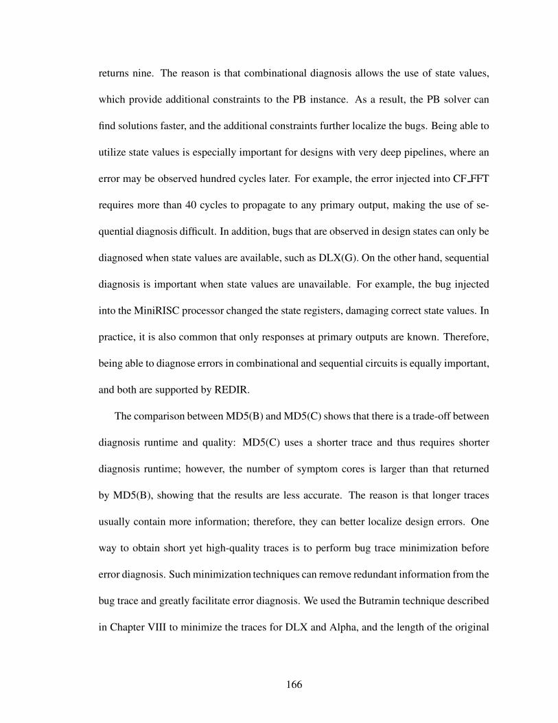
returns nine. The reason is that combinational diagnosis allows the use of state values,
which provide additional constraints to the PB instance. As a result, the PB solver can
find solutions faster, and the additional constraints further localize the bugs. Being able to
utilize state values is especially important for designs with very deep pipelines, where an
error may be observed hundred cycles later. For example, the error injected into CF FFT
requires more than 40 cycles to propagate to any primary output, making the use of se-
quential diagnosis difficult. In addition, bugs that are observed in design states can only be
diagnosed when state values are available, such as DLX(G). On the other hand, sequential
diagnosis is important when state values are unavailable. For example, the bug injected
into the MiniRISC processor changed the state registers, damaging correct state values. In
practice, it is also common that only responses at primary outputs are known. Therefore,
being able to diagnose errors in combinational and sequential circuits is equally important,
and both are supported by REDIR.
The comparison between MD5(B) and MD5(C) shows that there is a trade-off between
diagnosis runtime and quality: MD5(C) uses a shorter trace and thus requires shorter
diagnosis runtime; however, the number of symptom cores is larger than that returned
by MD5(B), showing that the results are less accurate. The reason is that longer traces
usually contain more information; therefore, they can better localize design errors. One
way to obtain short yet high-quality traces is to perform bug trace minimization before
error diagnosis. Such minimization techniques can remove redundant information from the
bug trace and greatly facilitate error diagnosis. We used the Butramin technique described
in Chapter VIII to minimize the traces for DLX and Alpha, and the length of the original
166

traces is shown in parentheses. In general, one trace is enough to localize the errors to a
small number of symptom cores, while additional traces may further reduce this number.
Case study: we use DLX(D) as an example to show the power of our error-diagnosis
techniques. Part of its RTL code is shown below:
always@(memstage or exstage or idstage or rs3rd or rs3rt or rs4rd or rs4rt or rsr31)
casex (memstage,exstage,idstage,rs3rd,rs3rt,rs4rd,rs4rt,rsr31)
‘ALUimm, ‘dc3, ‘dc3,‘dc,‘dc, ‘dc, ‘true,‘dc:
RSsel = ‘select stage3 bypass; // Buggy
......
In this example, the buggy code selects stage3 bypass, while the correct implementation
should select stage4. Error diagnosis returns two symptom cores: RSsel and ALUout.
Obviously, RSsel is the correct diagnosis. However, ALUout is also a correct diagnosis
because if the ALU can generate correct outputs even though the control signal is incorrect,
then the bug can also be fixed. However, this is not a desirable fix. This case study shows
that REDIR can suggest various ways to repair the same error, allowing the designer to
consider different possibilities in order to choose the best fix.
Simulation-Based Error Diagnosis
In this experiment, we performed simulation-based diagnosis using the algorithm de-
scribed in Section 9.2.2 with Insight, an experimental RTL symbolic simulator from [126].
Benchmarks Pipe and CF FFT were used in this experiment. Simulation took 23.8 and
162.9 seconds to generate SAT instances for these benchmarks, respectively. The SAT
solver included in Insight then solved the instances in 1 and 723 seconds respectively, and
167

Table 9.11: Error-correction results for RTL designsBench-mark Bug #Cores Resyn. #Fixes Runtimemark ID fixed method (sec)Pipe A 1 GDS 2214 1.0Pre norm A 1 GDS 4091 1.1
B 1 GDS 4947 2.4C 1 GDS 68416 5.6D 2 GDS 79358 7.1E 3 GDS 548037 41.6
MD5 A 1 GDS 33625 4.1B 0 GDS 0 3.86
CF FFT A 3 GDS 214800 141.6DLX A 0 GDS 0 1.3
B 3 GDS 5319430 111.2C 5 DPS 5 1.6D 3 DPS 3 1.6E 4 DPS 4 1.4F 2 DPS 2 2.9G 1 GDS 51330 0.7
Alpha A 5 DPS 5 7.9B 4 DPS 4 10.4C 3 DPS 3 8.5
it successfully identified the design errors. Note that currently, the SAT solver only returns
one, instead of all possible symptom cores. Although the runtime of simulation-based
approach is longer than the synthesis-based method, it does not require the design to be
synthesized in advance, thus saving the synthesizer runtime.
Error Correction
In our error-correction experiment, we applied the techniques described in Section
9.2.3 to fix the errors diagnosed in Table 9.9. We used combinational diagnosis in this
experiment, and corrected the error locations using the resynthesis methods described in
Chapter VI. We summarize the results in Table 9.11 where we indicate which of the two
synthesis techniques we used, either GDS or DPS. In the table, “#Cores fixed” is the num-
168

ber of symptom cores that can be corrected using our error-correction techniques, and
“#Fixes” is the number of ways to fix the errors. We applied GDS first in the experi-
ment, and observed that GDS often returns a large number of valid fixes that can correct
the design errors. One reason is that GDS performs exhaustive search to find new logic
expressions; therefore, it may find many different ways to produce the same signal. For
example, “A · B” and “A · (A ⊕ B)” are both returned even though they are equivalent.
Another reason is that we only diagnosed short bug traces, which may produce spurious
fixes: signatures of different variables are the same even though their functions are differ-
ent. As a result, we only report the first 100 fixes in our implementation, where the fixes
are sorted so that those with smaller number of logic operations are returned first. Due
to the exhaustive-search nature of GDS, memory usage of GDS may be high during the
search, as are the cases for benchmarks DLX (C-F) and Alpha. In these benchmarks, GDS
ran out of memory, and we relied on DPS to find fixes that can correct the errors. Since
DPS only returns one logic expression when fixing an error, the number of possible fixes
is significantly smaller.
Table 9.11 shows that we could not find valid fixes for benchmarks MD5(B) and
DLX(A). The reason is that the bugs in these benchmarks involve multi-bit variables.
For example, bug MD5(b) is an incorrect state transition for a 3-bit state register. Since
in this experiment we only consider the least-significant bits of such variables during er-
ror correction, we could not find a valid fix. This problem can be solved by inserting a
conditional assignment for every bit in a multi-bit variable.
169

Discussion of RTL Error-Repair Results
The RTL error-diagnosis results show that our error-modeling constructs and diagnosis
techniques can effectively localize design errors to a small number of symptom variables.
On the other hand, our error-correction results suggest that options to repair the diagnosed
errors abound. The reason is that the search space of error correction is much larger than
error diagnosis: there are various ways to synthesize a logic function. As a result, finding
high-quality fixes for a bug requires much more information than providing high-quality
diagnoses. Although this can be achieved by diagnosing longer or more numerous bug
traces, the runtime of REDIR will also increase.
This observation shows that automatic error correction is a much more difficult prob-
lem than automatic error diagnosis. In practice, however, engineers often find error di-
agnosis more difficult than error correction. It is common that engineers need to spend
days or weeks finding the cause of a bug. However, once the bug is identified, fixing it
may only take a few hours. To this end, our error-correction technique can also be used
to facilitate manual error repair, and it works as follows: (1) the engineer fixes the RTL
code manually to provide new logic functions for the symptom cores identified by error
diagnosis; and (2) REDIR simulates the new functions to check whether the signatures
of symptom cores can be generated correctly using the new functions. If the signatures
cannot be generated by the new functions, then the fix is invalid. In this way, engineers
can check the correctness of their fixes before running verification, which can accelerate
the manual error-repair process significantly.
The synthesis-based results show that our techniques can effectively handle designs
170

as large as 2000 lines of RTL code, which is approximately the size that an engineer
actively works on. Since synthesis tools are available in most companies, REDIR can be
used by engineers everyday to facilitate their debugging process. On the other hand, the
simulation-based results suggest that our techniques are promising. Once RTL symbolic
simulators become accessible to most companies, REDIR can automatically exploit their
simulation power to handle even larger designs.
9.4 Summary
In this chapter we empirically evaluated the effectiveness of the CoRe framework in re-
pairing functional errors in combinational gate-level netlists. In addition, we extended the
framework to repair errors in sequential circuits. This framework exploits both satisfiabil-
ity and observability don’t-cares, and it uses an abstraction-refinement scheme to achieve
better scalability. The experimental results show that CoRe can produce a modified netlist
which eliminates erroneous responses while maintaining correct ones. In addition, CoRe
only requires test vectors and correct output responses; therefore, it can be easily adopted
in most verification flows.
Other contributions in this chapter are the constructs and algorithms that provide a
fundamentally new way to diagnose and correct errors at the RTL, including: (1) an RTL
error modeling construct; (2) scalable error-diagnosis algorithms using Pseudo-Boolean
constraints, synthesis, and simulation; and (3) a novel error-correction technique using
signatures. To empirically validate our proposed techniques, we developed a new veri-
fication framework, called REDIR. To this end, our experiments with industrial designs
demonstrate that REDIR is efficient and scalable. In particular, designs up to a few thou-
171

sand lines of code (or 100K cells after synthesis) can be diagnosed within minutes with
high accuracy. The superior scalability, efficiency and accuracy of REDIR ensure that
it can be used by engineers in their everyday debugging tasks, which can fundamentally
change the RTL debugging process.
The comparison between gate-level and RTL error diagnosis shows that RTL bugs
should be fixed at the RTL because fixing the same errors at the gate level will become
much more difficult. To this end, REDIR can greatly enhance the RTL debugging process
to prevent bugs from escaping to the gate level, allowing most functional errors to be
caught and repaired at the RTL. Therefore, even if bugs still escape to the gate level, those
bugs will be more subtle and should require smaller changes to the netlist. This will allow
gate-level error-repair techniques to work more effectively.
172

CHAPTER X
Incremental Verification for Physical Synthesis
As interconnect increasingly dominates delay and power at the latest technology nodes,
much effort is invested in physical synthesis optimizations, posing great challenges in val-
idating the correctness of such optimizations. Common design methodologies that delay
the verification of physical synthesis transformations until the completion of the design
phase are no longer sustainable because it makes the isolation of potential errors extremely
challenging. Since the design’s functional correctness should not be compromised, engi-
neers dedicate considerable resources to ensure the correctness at the expense of improving
other aspects of design quality. To address these challenges, we propose a fast incremen-
tal verification system for physical synthesis optimizations, called InVerS, which includes
capabilities for error detection and diagnosis. This system helps engineers discover errors
earlier, which simplifies error isolation and correction, thereby reducing verification effort
and enabling more aggressive optimizations to improve performance.
10.1 Background
In this section we first take a closer look at the current physical synthesis flow. Next,
we describe a powerful physical synthesis technique called retiming. Retiming reposi-
173

tions registers in a design and can perform optimizations not achievable by combinational
resynthesis methods. Our methodologies to verify the correctness of these optimizations
will be presented in the next section.
10.1.1 The Current Physical Synthesis Flow
Post-placement optimizations have been studied and used extensively to improve cir-
cuit parameters such as power and timing, and these techniques are often called physical
synthesis. In addition, it is sometimes necessary to change the layout manually in or-
der to fix bugs or optimize specific objectives; this process is called Engineering Change
Order (ECO). Physical synthesis is commonly performed using the following flow: (1)
perform accurate analysis of the optimization objective, (2) select gates to form a region
for optimization, (3) resynthesize the region to optimize the objective, and (4) perform
legalization to repair the layout. The work by Lu et al. [82] and Changfan et al. [41] are
all based on this flow.
Given that subtle and unexpected bugs still appear in physical synthesis tools today
[9], verification must be performed to ensure the correctness of the circuit. However,
verification is typically slow; therefore, it is often performed after hundreds or thousands
of optimizations, as shown in Figure 10.1. As a result, it is difficult to identify the circuit
modification that introduced the bug. In addition, debugging the circuit at this design stage
is often difficult because engineers are unfamiliar with the automatically generated netlist.
As we will show later, InVerS addresses these problems by providing a fast incremental
verification technique.
174

Figure 10.1: The current post-layout optimization flow. Verification is performed after thelayout has undergone a large number of optimizations, which makes debug-ging difficult.
10.1.2 Retiming
Retiming is a sequential logic optimization technique that repositions the registers in
a circuit while leaving the combinational cells unchanged [75, 102]. It is often used to
minimize the number of registers in a design or to reduce a circuit’s delay. For example,
the circuit in Figure 10.4(b) is a retimed version of the circuit in Figure 10.4(a) that opti-
mizes delay. Although retiming is a powerful technique, ensuring its correctness imposes
a serious problem on verification because sequential equivalence checking is orders of
magnitude more difficult than combinational equivalence checking [63]. As a result, the
runtime of sequential verification is often much longer than that of combinational verifi-
cation, if it ever finishes. This problem will be addressed in Section 10.2.2.
175

10.2 Incremental Verification
We provide a robust incremental verification package that is composed of a logic sim-
ulator, a SAT-based formal equivalence checker, and our innovative similarity metric be-
tween a circuit and its revision. In this section we define our similarity metrics, and then
describe our overall verification methodology.
10.2.1 New Metric: Similarity Factor
We define the similarity factor as an estimate of the similarity between two netlists,
ckt1 and ckt2. This metric is based on simulation signatures of individual signals, and those
signatures can be calculated using fast simulation. Let N be the total number of signals
(wires) in both circuits. Out of those N signals, we distinguish M matching signals — a
signal is considered matching if and only if both circuits include signals with an identical
signature. The similarity factor between ckt1 and ckt2 is then M/N. In other words:
similarity f actor =number o f matching signals
total number o f signals(10.1)
We also define the difference factor as (1− similarity f actor).
Example 10 Consider the two netlists shown in Figure 10.2, where the signatures are
shown above the wires. There are 10 signals in the netlists, and 7 of them are matching.
As a result, the similarity factor is 7/10= 70%, and the difference factor is 1 - 7/10 = 30%.
Intuitively, the similarity factor of two identical circuits should be 100%. If a circuit
is changed slightly but is still mostly equivalent to the original version, then its similarity
factor should drop only slightly. For example, Figure 10.3(a) shows a netlist where a
176

Figure 10.2: Similarity factor example. Note that the signatures in the fanout cone of thecorrupted signal are different.
region of gates is resynthesized correctly. Since only the signatures in that region will be
affected, the similarity factor only drops slightly. However, if the change greatly affects
the circuit’s function, the similarity factor can drop significantly, depending on the number
of signals affected by the change. As Figure 10.3(b) shows, when a bug is introduced
by resynthesis, the signatures in the output cone of the resynthesized region will also be
different, causing a larger drop in similarity factor. However, two equivalent circuits may
be dissimilar, e.g., a Carry-Look-Ahead adder and a Kogge-Stone adder. Therefore, the
similarity factor should be used in incremental verification and cannot replace traditional
verification techniques.
10.2.2 Verification of Retiming
A signature represents a fraction of a signal’s truth table, which in turn describes the
information flow within a circuit. While retiming may change the clock cycle that certain
signatures are generated, because combinational cells are preserved, most generated sig-
natures should be identical. Figure 10.4 shows a retiming example from [38], where (a) is
the original circuit and (b) is the retimed circuit. A comparison of signatures between the
177

(a)
(b)Figure 10.3: Resynthesis examples: (a) the gates in the rectangle are resynthesized cor-
rectly, and their signatures may be different from the original netlist; (b) anerror is introduced during resynthesis, and the signatures in the output coneof the resynthesized region are also different, causing a significant drop insimilarity factor.
circuits shows that the signatures in (a) also appear in (b), although the cycles in which
they appear may be different. For example, the signatures of wire w (bold-faced) in the
retimed circuit appear one cycle earlier than those in the original circuit because the regis-
ters were moved later in the circuit. Otherwise, the signatures of (a) and (b) are identical.
This phenomenon becomes more obvious when the circuit is unrolled, as shown in Figure
10.5. Since the maximum absolute lag in this example is 1, retiming only affects gates in
the first and the last cycles, leaving the rest of the circuits identical. As a result, signatures
generated by the unaffected gates should also be identical. Based on this observation, we
extend our similarity factor to sequential verification, called sequential similarity factor,
as follows. Assume two netlists, ckt1 and ckt2, where the total number of signals (wires)
in both circuits is N. After simulating C cycles, N ×C signatures will be generated. Out of
those signatures, we distinguish M matching signatures. The sequential similarity factor
178

between ckt1 and ckt2 is then M/(N ×C). In other words:
sequential similarity f actor =number o f matching signatures f or all cycles
total number o f signatures f or all cycles(10.2)
(a)
(b)Figure 10.4: A retiming example: (a) is the original circuit, and (b) is its retimed version.
The tables above the wires show their signatures, where the nth row is for thenth cycle. Four traces are used to generate the signatures, producing four bitsper signature. Registers are represented by black rectangles, and their initialstates are 0. As wire w shows, retiming may change the cycle that signaturesappear, but it does not change the signatures (signatures shown in boldfaceare identical).
10.2.3 Overall Verification Methodology
As mentioned in Section 10.1.1, traditional verification is typically performed after a
batch of circuit modifications because it is very demanding and time consuming. As a
result, once a bug is found, it is often difficult to isolate the change that introduced the bug
179

(a)
(b)Figure 10.5: Circuits in Figure 10.4 unrolled three times. The cycle in which a signal
appears is denoted using subscript “@”. Retiming affects gates in the firstand the last cycles (marked in dark gray), while the rest of the gates arestructurally identical (marked in light gray). Therefore, only the signaturesof the dark-gray gates will be different.
because hundreds or thousands of changes have been made. Similarity factor addresses
this problem by pointing out the changes that might have corrupted the circuit. As de-
scribed in previous subsections, a change that greatly affects the circuit’s function will
probably cause a sudden drop in the similarity factor. By monitoring the change in sim-
ilarity factor after every circuit modification, engineers will be able to know when a bug
might have been introduced and traditional verification should be performed. Using the
techniques that we developed, we propose the InVerS incremental verification methodol-
ogy as shown in Figure 10.6, and it works as follows:
1. After each change to the circuit, the similarity factor between the new and the origi-
nal circuit is calculated. Running average and standard deviation of the past 30 simi-
larity factors are used to determine whether the current similarity factor has dropped
180

Figure 10.6: Our InVerS verification methodology. It monitors every layout modificationto identify potential errors and calls equivalence checking when necessary.Our functional error repair techniques can be used to correct the errors whenverification fails.
significantly. Empirically, we found that if the current similarity factor drops below
the average by more than two standard deviations, then it is likely that the change
introduced a bug. This number, however, may vary among different benchmarks and
should be empirically determined.
2. When similarity factor indicates a potential problem, traditional verification should
be performed to verify the correctness of the executed circuit modification.
3. If verification fails, our functional error repair tools can be used to repair the errors.
Since InVerS monitors drops in similarity factors, rather than the absolute values of
similarity factors, the structures of the netlists become less relevant. Therefore, InVerS
can be applied to a variety of netlists, potentially with different error-flagging thresholds.
As Section 10.3 shows, the similarity factor exhibits high accuracy for various practical
designs and allows our verification methodology to achieve significant speed-up over tra-
ditional techniques.
181

10.3 Experimental Results
We implemented InVerS using OpenAccess 2.2 and OAGear 0.96 [140]. Our testcases
were selected from IWLS’05 benchmarks [138] based on designs from ISCAS’89 and
OpenCores suites, whose characteristics are summarized in Table 10.1. In the table, the
average level of logic is calculated by averaging the logic level of 30 randomly selected
gates. The number of levels of logic can be used as an indication of the circuit’s com-
plexity. We conducted all our experiments on an AMD Opteron 880 Linux workstation.
The resynthesis package used in our experiments is ABC from UC Berkeley [127]. In this
section we report results on combinational and sequential verification, respectively.
Table 10.1: Characteristics of benchmarks.Benchmark Cell Ave. level Function
count of logicS1196 483 6.8 ISCAS’89USB phy 546 4.7 USB 1.1 PHYSASC 549 3.7 Simple asynchronous serial controllerS1494 643 6.5 ISCAS’89I2C 1142 5.5 I2C master controllerDES AREA 3132 15.1 DES cipher (area optimized)SPI 3227 15.9 SPI IPTV80 7161 18.7 8-Bit microprocessorMEM ctrl 11440 10.1 WISHBONE memory controllerPCI bridge32 16816 9.4 PCI bridgeAES core 20795 11.0 AES cipherWB conmax 29034 8.9 WISHBONE Conmax IP coreDES perf 98341 13.9 DES cipher (performance optimized)
10.3.1 Verification of Combinational Optimizations
Evaluation of the similarity factor: in our first experiment, we performed two types of
circuit modifications to evaluate the effectiveness of the similarity factor for combinational
verification. In the first type, we randomly injected an error into the circuit according to
182

Abadir’s error model (see Section 5.1.4), which includes the errors that occur frequently
in gate-level netlists. This mimics the situation where a bug has been introduced. In the
second type, we extracted a subcircuit from the benchmark, which was composed of 2-20
gates, and performed resynthesis of the subcircuit using ABC with the “resyn” command
[127]. This is similar to the physical synthesis or ECO flow described in Section 10.1.1,
where gates in a small region of the circuit are changed. We then calculated the similarity
factor after each circuit modification for both types of circuit modifications and compared
their difference. Thirty samples were used in this experiment, and the results are summa-
rized in Table 10.2. From the results, we observe that both types of circuit modifications
lead to decreases in similarity factor. However, the decrease is much more significant
when an error is injected. As d1 shows, the standardized differences in the means of most
benchmarks are larger than 0.5, indicating that the differences are statistically significant.
Since resynthesis tests represent the norm and error-injection tests are anomalies, we also
calculated d2 using only SDr. As d2 shows, the mean similarity factor drops more than
two standard deviations when an error is injected for most benchmarks. This result shows
that the similarity factor is effective in predicting whether a bug has been introduced by
the circuit modification. Nonetheless, in all benchmarks, the maximum similarity factor
for error-injection tests is larger than the minimum similarity factor for resynthesis tests,
suggesting that the similarity factor cannot replace traditional verification and should be
used as an auxiliary technique.
The impact of cell count on the similarity factor: in order to study other aspects that may
affect the similarity factor, we further analyze our results by plotting the factors against
183

Table 10.2: Statistics of similarity factors for different types of circuit modifications.Benchmark Similarity factor (%)
Resynthesized One error injected d1 d2Meanr Minr Maxr SDr Meane Mine Maxe SDe
USB phy 99.849 99.019 100.000 0.231 98.897 91.897 99.822 1.734 0.969 4.128SASC 99.765 99.119 100.000 0.234 97.995 90.291 99.912 2.941 1.115 7.567I2C 99.840 99.486 100.000 0.172 99.695 98.583 100.000 0.339 0.567 0.843SPI 99.906 99.604 100.000 0.097 99.692 96.430 99.985 0.726 0.518 2.191TV80 99.956 99.791 100.000 0.050 99.432 94.978 100.000 1.077 0.930 10.425MEM ctrl 99.984 99.857 100.000 0.027 99.850 97.699 100.000 0.438 0.575 4.897PCI bridge32 99.978 99.941 100.000 0.019 99.903 97.649 99.997 0.426 0.338 3.878AES core 99.990 99.950 100.000 0.015 99.657 98.086 99.988 0.470 1.372 21.797WB conmax 99.984 99.960 100.000 0.012 99.920 99.216 99.998 0.180 0.671 5.184DES perf 99.997 99.993 100.000 0.002 99.942 99.734 100.000 0.072 1.481 23.969
Thirty tests were performed in this experiment, whose means, minimal values (Min), maximumvalues (Max), and standard deviations (SD) are shown. The last two columns show the standardizeddifferences in the means: d1 is calculated using the average of both SDe and SDr, while d2 usesonly SDr.
the cell counts of the benchmarks. To make the figure clearer, we plot the difference factor
instead of the similarity factor. We notice that by construction, the difference factor tends
to reduce with the increase in design size, which makes the comparison among different
benchmarks difficult. In order to compensate this effect, we assume that the bug density
is 1 bug per 1,000 gates and adjust our numbers accordingly. The plot is shown in Figure
10.7, where the triangles represent data points from error-injection tests, and the squares
represent resynthesis tests. The linear regression lines of two data sets are also shown.
From the figure, we observe that the difference factor tends to increase with the cell count
for error-injection tests. The increase for resynthesis tests, however, is less significant.
As a result, the difference factor of error-injected circuits (triangle data points) will grow
faster than that of resynthesized circuits (square data points) when cell count increases,
creating larger discrepancy between them. This result shows that the similarity factor
will drop more significantly for larger designs, making it more accurate when applied to
practical designs, which often have orders of magnitude more cells than the benchmarks
used in our tests.
184

Figure 10.7: The relationship between cell count and the difference factor. The linearregression lines of the datapoints are also shown.
The impact of level of logic on the similarity factor: here we perform similar analysis
using the number of levels of logic as the independent variable. The slopes of the linear
regression lines for the error-injection tests and the resynthesis tests are 0.236 and 0.012,
respectively. The difference in slopes shows that the difference factor grows faster when
the number of levels of logic increases, indicating that the similarity factor will be more
effective when designs become more complicated. This behavior is preferable because
complicated designs are often more difficult to verify.
To study the impact of the number of levels of logic on the difference factor within
a benchmark, we plotted the difference factor against the number of levels of logic using
benchmark DES perf in Figure 10.8. The logarithmic regression line for the error-injection
tests are also shown. As the figure suggests, the difference factor decreases with the in-
crease in the number of levels of logic. The reason is that gates with smaller numbers of
levels of logic have larger downstream logic, therefore larger numbers of signatures will
be affected. As a result, the difference factor will be larger. That the variance explained is
large (0.7841) suggests that this relation is strong. However, some benchmarks do not ex-
185

hibit this trend. For example, the variance explained for benchmark TV18 is only 0.1438.
For benchmarks that exhibit this trend, the similarity factor provides a good predication of
the location of the bug: a larger drop in the similarity factor indicates that the bug is closer
to primary inputs.
Figure 10.8: The relationship between the number of levels of logic and the differencefactor in benchmark DES perf. The x-axis is the level of logic that the circuitis modified. The logarithmic regression line for the error-injection tests isalso shown.
To evaluate the effectiveness of our incremental verification methodology described in
Section 10.2.3, we assumed that there is 1 bug per 100 circuit modifications, and then we
calculated the accuracy of our methodology. We also report the runtime for calculating
the similarity factor and the runtime for equivalence checking of each benchmark. Since
most circuit modifications do not introduce bugs, we report the runtime when equivalence
is maintained. The results are summarized in Table 10.3. From the results, we observe
that our methodology has high accuracy for most benchmarks. In addition, the results
show that calculating the similarity factor is significantly faster than performing equiva-
lence checking. For example, calculating the similarity factor of the largest benchmark
(DES perf) takes less than 1 second, while performing equivalence checking takes about
186

78 minutes. Due to the high accuracy of the similarity factor, our incremental verification
technique identifies more than 99% of errors, rendering equivalence checking unnecessary
in those cases and providing a more than 100X speed-up.
Table 10.3: The accuracy of our incremental verification methodology.Benchmark Cell Accuracy Runtime(sec)
count EC SFUSB phy 546 92.70% 0.19 <0.01SASC 549 89.47% 0.29 <0.01I2C 1142 95.87% 0.54 <0.01SPI 3227 96.20% 6.90 <0.01TV80 7161 96.27% 276.87 0.01MEM ctrl 11440 99.20% 56.85 0.03PCI bridge32 16816 99.17% 518.87 0.04AES core 20795 99.33% 163.88 0.04WB conmax 29034 92.57% 951.01 0.06DES perf 98341 99.73% 4721.77 0.19
1 bug per 100 circuit modifications is assumed in this experiment. Runtime for similarity-factorcalculation (SF) and equivalence checking (EC) is also shown.
10.3.2 Sequential Verification of Retiming
In our second experiment, we implemented the retiming algorithm described in [75]
and used our verification methodology to check the correctness of our implementation.
This methodology successfully identified several bugs in our initial implementation. In our
experience, most bugs were caused by incorrect netlist modifications when repositioning
the registers, and a few bugs were due to erroneous initial state calculation. Examples of
the bugs include: (1) incorrect fanout connection when inserting a register to a wire which
already has a register; (2) missing/additional register; (3) missing wire when a register
drives a primary output; and (4) incorrect state calculation when two or more registers are
connected in a row.
To quantitatively evaluate our verification methodology, we ran each benchmark us-
187

ing the correct implementation and the buggy version to calculate their respective SSFs,
where 10 cycles were simulated. The results are summarized in Table 10.4, which shows
that the sequential similarity factors for retimed circuits are 100% for most benchmarks.
As explained in Section 10.2.2, only a few signatures should be affected by retiming.
Therefore, the drop in similarity factor should be very small, making sequential similarity
factor especially accurate for verifying the correctness of retiming. This phenomenon can
also be observed from Table 10.5, where the accuracy of our verification methodology is
higher than 99% for most benchmarks. To compare our methodology with formal equiv-
alence checking, we also show the runtime of a sequential equivalence checker based
on bounded-model-checking in Table 10.5. This result shows that our methodology is
more beneficial for sequential verification than combinational because sequential equiv-
alence checking requires much more runtime than combinational. Since the runtime to
compute sequential similarity factor remains small, our technique can still be applied after
every retiming optimization and thus eliminating most unnecessary sequential equivalence
checking calls.
Table 10.4: Statistics of sequential similarity factors for retiming with and without errors.Benchmark Sequential similarity factor (%)
Retiming without errors Retiming with errorsMeanr Minr Maxr SDr Meane Mine Maxe SDe
S1196 100.0000 100.0000 100.0000 0.0000 98.3631 86.7901 100.0000 3.0271USB phy 100.0000 100.0000 100.0000 0.0000 99.9852 99.6441 100.0000 0.0664SASC 99.9399 99.7433 100.0000 0.0717 99.9470 99.3812 100.0000 0.1305S1494 100.0000 100.0000 100.0000 0.0000 99.0518 94.8166 99.5414 1.5548I2C 100.0000 100.0000 100.0000 0.0000 99.9545 99.6568 100.0000 0.1074DES AREA 100.0000 100.0000 100.0000 0.0000 95.9460 69.1441 100.0000 6.3899
Thirty tests were performed in this experiment, whose means, minimal values (Min), maximumvalues (Max), and standard deviations (SD) are shown.
188

Table 10.5: Runtime of sequential similarity factor calculation (SSF) and sequential equiv-alence checking (SEC).
Benchmark Cell DFF Accuracy Runtime (sec)count count SEC SSF
S1196 483 18 99.87% 5.12 0.42USB phy 546 98 99.10% 0.41 0.34SASC 549 117 95.80% 5.16 0.56S1494 643 6 99.47% 2.86 0.45I2C 1142 128 99.27% 2491.01 1.43DES AREA 3132 64 99.97% 49382.20 14.50
Accuracy of our verification methodology is also reported, where 1 bug per 100 retiming optimiza-tions is assumed.
10.4 Summary
In this work we developed a novel incremental equivalence verification system, InVerS,
with a particular focus on improving design quality and engineers’ productivity. The high
performance of InVerS allows designers to invoke it frequently, possibly after each circuit
transformation. This allows errors to be detected sooner, when they can be more easily
pinpointed and resolved. The scalability of InVerS stems from the use of fast simulation,
which can efficiently calculate our proposed similarity factor metric to spot potential dif-
ferences between two versions of a design. The areas where we detect a low similarity are
spots potentially hiding functional bugs that can be subjected to more expensive formal
techniques. The experimental results show that InVerS achieves a hundred-fold runtime
speed-up on large designs compared to traditional techniques for similar verification goals.
Our methodology and algorithms promise to decrease the number of latent bugs released
in future digital designs and to facilitate more aggressive performance optimizations, thus
improving the quality of electronic design in several categories.
189

CHAPTER XI
Post-Silicon Debugging and Layout Repair
Modern IC designs have reached unparalleled levels of overall complexity, and thor-
ough verification is becoming more difficult. Furthermore, the verification problem is
exacerbated by the highly competitive market which requires shorter time-to-market. As
a result, design errors are more likely to escape verification in the early stage of the design
flow and are found after layout has been finished; or even worse, after the chip has been
taped-out. Needless to say, these errors must be fixed before the IC can reach the market.
Fixing such errors is often costly, especially when the chip has been taped-out. The key
to reduce this cost is to preserve as much previous effort spent on the design as possible.
In this chapter we present error-repair techniques that support the post-silicon debugging
methodology described in Section 4.4. However, these techniques can be applied to pre-
silicon layout optimization or error repair as well.
As mentioned in Section 2.4, design errors that occur post-silicon can be functional
or electrical, and various physical synthesis techniques may be used to fix such errors.
However, there is no metric to measure the impact of a physical synthesis technique on
the layout. In this chapter, we first define and explore the concepts of physical safeness
190

and logical soundness to measure such an impact. We observe from this analysis that most
existing physical synthesis techniques do not allow post-silicon metal fix, and those sup-
port metal fix have limited error-repair capabilities. Therefore, we propose a SafeResynth
technique that is more powerful yet has little impact on a layout. The next section then
describes how SafeResynth can be applied to repair post-silicon electrical errors. In addi-
tion, the section also illustrates our new functional and electrical error repair techniques.
This chapter concludes with experimental results and a brief summary.
11.1 Physical Safeness and Logical Soundness
The concept of physical safeness is used to describe the impact of an optimization tech-
nique on the placement of a circuit. Physically safe techniques only allow legal changes
to a given placement; therefore, accurate analysis such as timing and congestion can be
performed. Such changes are safe because they can be rejected immediately if the layout
is not improved. On the other hand, unsafe techniques allow changes that produce a tem-
porarily illegal placement. As a result, their evaluation is delayed, and it is not possible
to reliably decide if the change can be accepted or must be rejected until later. Therefore,
the average quality of unsafe changes may be worse than that of accepted safe changes. In
addition, other physical parameters, such as wirelength or via count, may be impacted by
unsafe transformations.
Similar to physical safeness, logical soundness is used to describe the perturbation to
the logic made by the optimization techniques. Techniques that do not change the logic
usually do not require verification. Examples for this type of optimization include gate
sizing and buffer insertion. Techniques that change the logic of the circuit may require
191

verification to ensure their correctness. For example, optimizations based on reconnect-
ing wires require verification because any bug in the optimization process may change
the circuit’s behavior. Since local changes to combinational logic can be verified easily
using equivalence checking, they are considered logically sound. However, small changes
to sequential logic often have global implications and are much more difficult to verify,
therefore we do not classify them as logically sound techniques. These techniques include
the insertion of clocked repeaters and the use of retiming.
11.1.1 Physically Safe Techniques
Symmetry-based rewiring is one of the few physical synthesis techniques that is
physically safe in nature. As described in Chapter VII, it exploits symmetries in logic
functions, looking for pin reconnections that improve the optimization objective. For ex-
ample, the inputs to an AND gate can be swapped without changing its logic function.
Since only wiring is changed in this technique, the placement is always preserved. An
example of symmetry-based rewiring is given in Figure 11.1(a).
The advantage of physically safe techniques is that the effects of any change are imme-
diately measurable, therefore the change can be accepted or rejected reliably. As a result,
circuit parameters will not deteriorate after optimization and no timing convergence prob-
lem will occur. However, the improvement gained from these techniques is often limited
because they cannot aggressively modify the logic or use larger-scale optimizations. For
example, in [28] timing improvement measured before routing is typically less than 10%.
192

11.1.2 Physically Unsafe Techniques
Traditional physical synthesis techniques are physically unsafe because they create
cell overlaps and thus prevent immediate evaluation of changes. Although some of these
techniques can be applied in a safe way, they may lose their strength. It follows that
existing physical synthesis tools usually rely on unsafe techniques, planning to correct
potentially illegal changes after the optimization phase is complete. A classification of
these techniques and their impact on logic are discussed below.
Gate sizing and buffer insertion are two important techniques that do not change the
logic, as shown in Figure 11.1(b) and Figure 11.1(d). Gate sizing chooses the size of the
gates carefully so that signal delay in wires can be balanced with gate delay, and the gates
have enough strength to drive the wires. Buffer insertion adds buffers to drive long wires.
The work by Kannan et al. [69] is based on these techniques.
Gate relocation moves gates on critical paths to better locations and also does not
change the logic. An example of gate relocation is given in Figure 11.1(c). Ajami et
al. [4] utilize this technique by performing timing-driven placement with global routing
information using the notion of movable Steiner points. They formulate the simultaneous
placement and routing problem as a mathematical program. The program is then solved
by Han-Powell method.
Gate replication is another technique that can improve circuit timing without chang-
ing the logic. As Figure 11.1(e) shows, by duplicating g5, the delay to g1 and g9 can be
reduced. Hrkic et al. [60] proposed a placement-coupled approach based on such tech-
nique. Given a placed circuit, they first extract replication trees from the critical paths
193

after timing analysis, and then they perform embedding and post-unification to determine
the gates that should be duplicated as well as their locations. Since duplicated gates may
overlap with existing gates, at the end of the process, timing-driven legalization is ap-
plied. Although their approach improves timing by 1-36%, it also increases route length
by 2-28%.
(a) Symmetry-based rewiring. (b) Gate sizing.
(c) Gate relocation. (d) Buffer insertion.
(e) Gate duplication.
Figure 11.1: Several distinct physical synthesis techniques. Newly-introduced overlapsare removed by legalizers after the optimization phase has completed.
Traditional rewiring techniques based on addition or removal of redundant wires are
not physically safe. The basic idea is to add one or more redundant wires to make a target
wire redundant so that it becomes removable. Since gates must be modified to reflect the
changes in wires, cell overlaps may occur. The work in [40] utilizes this technique using
194

an ATPG reasoning approach.
Optimization techniques discussed so far can be made physically safe by rejecting all
changes that create new overlaps. For example, this would allow inserting buffers only in
overlap-free sites. However, the prevailing practice for these and many other optimizations
is to first allow overlaps and then call a legalizer to fix the overlaps. According to our
definition, this is physically unsafe. In other words, depending on how many overlaps are
introduced, how powerful and how accurate the legalizer is, the physical parameters of the
circuit may improve or deteriorate.
Traditional restructuring focuses on directing the synthesis process using timing in-
formation obtained from a placed or routed circuit. It is more aggressive in that it may
change the logic structure as well as the placement. This technique reflects the fact that
timing-driven synthesis requires accurate timing, which can only be obtained from a placed
circuit. However, a circuit cannot be placed unless it is synthesized. Restructuring attempts
to bridge the gap between these two different stages in circuit design.
A typical restructuring flow includes: (1) obtaining accurate timing analysis results
from a placed or routed design, (2) identifying critical paths in the design, (3) selecting
gates from the critical paths to form critical regions, (4) performing timing-driven resyn-
thesis on the critical regions, and (5) calling legalizers to remove gate overlaps that may
be created during the process. This process is repeated until timing closure is achieved.
The work by Lu et al. [81], Vaishnav et al. [111] and Changfan et al. [41] is all based on
this flow with emphasis on different aspects. For example, the work by Vaishnav focuses
on eliminating late-arriving events identified by symbolic simulation, while Changfan an-
195

alyzes the effects of routing on timing and utilizes them in his resynthesis and incremental
placement engines.
Traditional restructuring is usually physically unsafe. For example, evaluation of
new cell locations cannot be done reliably for technology-independent restructuring un-
less technology mapping is also performed. Moreover, restructuring techniques based on
AIGs are likely to be unsafe because node mergers performed in an AIG may distort a
given placed circuit [127]. As a result, the effects of the changes are not immediately
measurable. Although carefully designed techniques can be used to alleviate this prob-
lem [72, 78, 83], it is difficult to be eliminated altogether. The strength and safeness of
these techniques are summarized in Table 11.1. The two physically safe techniques will
be adapted to repair electrical errors in Section 11.4.
Table 11.1: Comparison of a range of physical synthesis techniques in terms of physicalsafeness and optimization potential.
Techniques Physical Optimizationsafeness potential
Symmetry-based rewiring Safe LowSafeResynth Safe MediumATPG-based rewiring, buffer insertion, Unsafe∗ Lowgate sizing, gate relocationGate replication Unsafe∗ MediumRestructuring Unsafe High
Low potential means that only local optimizations are possible, and high potential means that largescale optimizations are possible. ∗Note: some of these techniques could be made safe but popularimplementations use them in an unsafe fashion, allowing gate overlap.
11.2 New Resynthesis Technique — SafeResynth
Our safe physical synthesis approach, SafeResynth, is discussed in detail in this sec-
tion. It uses signatures (see Section 5.1.1) produced by simulation to identify potential
196

resynthesis opportunities, whose correctness are then validated by equivalence checking
[127]. Since our goal is layout optimization and error repair, we can prune some of the op-
portunities based on their improvement potential before formally verifying them. To this
end, we propose pruning techniques based on physical constraints and logical compatibil-
ity among signatures. SafeResynth is powerful in that it does not restrict resynthesis to
small geometric regions or small groups of adjacent wires. It is safe because the produced
placement is always legal and the effect can be evaluated immediately.
11.2.1 Terminology
A signature is a bit-vector of simulated values of a wire. Given the signature st of a
wire wt to be resynthesized, and a certain gate g1, a wire w1 with signature s1 is said to
be compatible with wt if it is possible to generate st using g1 with signature s1 as one of
its inputs. In other words, it is possible to generate wt from w1 using g1. For example, if
s1 = 1, st = 1 and g1 = AND, then w1 is compatible with wt using g1 because it is possible
to generate 1 on an AND’s output if one of its inputs is 1. However, if s1 = 0, then w1 is
not compatible with wt using g1 because it is impossible to obtain 1 on an AND’s output
if one of its inputs is 0 (see Figure 11.4).
A controlling value of a gate is the value that fully specifies the gate’s output when
applied to one input of the gate. For example, 0 is the controlling value for AND because
when applied to the AND gate, its output is always 0 regardless of the value of other inputs.
When two signatures are incompatible, that can often be traced to a controlling value in
some bits of one of the signatures.
197

11.2.2 SafeResynth Framework
The SafeResynth framework is outlined in Figure 11.2, and an example is shown in
Figure 11.3. In this section we illustrate how timing can be optimized; however, Safe-
Resynth can also be used to optimize other circuit parameters or repair post-silicon errors.
Initially, library contains all the gates to be used for resynthesis. We first generate a
signature for each wire by simulating certain input patterns. In order to optimize timing,
wiret in line 2 will be selected from wires on the critical paths in the circuit. Line 3 restricts
our search of potential resynthesis opportunities according to certain physical constraints,
and lines 4-5 further prune our search space based on logical soundness. After a valid
resynthesis option is found, we try placing the gate on various overlap-free sites close to
a desired location in line 6 and check their timing improvements. In this process, more
than one gate may be added if there are multiple sinks for wiret , and the original driver of
wiret may be replaced. In line 10 we remove redundant gates and wires that may appear
because wire′ts original driver may no longer drive any wire, which often initiates a chain
of further simplifications.
11.2.3 Search-Space Pruning Techniques
In order to resynthesize a target wire (wiret) using an n-input gate in a circuit con-
taining m wires, the brute force technique needs to check(m
n)
combinations of possible
inputs, which can be very time-consuming for n > 2. Therefore it is important to prune
the number of wires to try.
When the objective is to optimize timing, the following physical constraints can be
used in line 3 of the framework: (1) wires with arrival time later than that of wiret are
198

1. Simulate patterns and generate a signature for each wire.2. Determine wiret to be resynthesized and retrieve wiresc from the circuit.3. Prune wiresc according to physical constraints.4. Foreach gate ∈ library with inputs selected from combinations of compatible
wires ∈ wiresc.5. Check if wiret ’s signature can be generated using gate with its inputs’ signatures.
If not, try next combination.6. If so, do restructuring using gate by placing it on overlap-free sites close to the
desired location.7. If timing is improved, check equivalency. If not equivalent, try next combination
of wires.8. If equivalent, a valid restructuring is found.9. Use the restructuring with maximum delay improvement for resynthesis.
10. Identify and remove gates and wires made redundant by resynthesis.Figure 11.2: The SafeResynth framework.
discarded because resynthesis using them will only increase delay; and (2) wires that are
too far away from the sinks of wiret are abandoned because the wire delay will be too
large to be beneficial. We set this distance threshold to twice the HPWL (Half-Perimeter
WireLength) of wiret .
In line 4 logical compatibility is used to prune the wires that need to be tried. Wires not
compatible with wiret using gate are excluded from our search. Figure 11.4 summarizes
how compatibilities are determined given a gate type, the signatures of wiret and the wire
to be tested (wire1).
To accelerate compatibility testing, we use the one-count, i.e., the number of 1s in the
signature, to filter out unpromising candidates. For example, if gate==OR and the one-
count of wiret is smaller than that of wire1, then these two wires are incompatible because
OR will only increase one-count in the target wire. This technique can be applied before
bit-by-bit compatibility test to detect incompatibility faster.
Our pruned search algorithm that implements lines 4-5 of the framework is outlined in
199

Figure 11.3: A restructuring example. Input vectors to the circuit are shown on the left.Each wire is annotated with its signature computed by simulation on thosetest vectors. We seek to compute signal w1 by a different gate, e.g., in termsof signals w2 and w3. Two such restructuring options (with new gates) areshown as gn1 and gn2. Since gn1 produces the required signature, equivalencechecking is performed between wn1 and w1 to verify the correctness of thisrestructuring. Another option, gn2, is abandoned because it fails our compat-ibility test.
Gate type wiret wire1 ResultNAND 0 0 IncompatibleNOR 1 1 IncompatibleAND 1 0 IncompatibleOR 0 1 Incompatible
XOR/XNOR Any Any CompatibleFigure 11.4: Conditions to determine compatibility: wiret is the target wire, and wire1 is
the potential new input of the resynthesized gate.
Figure 11.5. It is specifically optimized for two-input gates and is a special version of the
GDS algorithm shown in Section 6.3. Wiret is the target wire to be resynthesized, wiresc
are wires selected according to physical constraints, and library contains gates used for
resynthesis. All wires in the fanout cone of wiret are excluded in the algorithm to avoid
the formation of combinational loops.
In Figure 11.5, function compatible returns wires in wiresg that are compatible with
wiret given gate. Function get potential wires returns wires in wiresd that are capable of
generating the signature of wiret using gate and wire1, and its algorithm is outlined in Fig-
200
Function pruned search(wiret ,wiresc, library)1 foreach gate ∈ library2 wiresg = compatible(wiret ,wiresc,gate);3 foreach wire1 ∈ wiresg4 wiresd = get potential wires(wiret ,wire1,wiresg,gate);5 foreach wire2 ∈ wiresd6 restructure using gate, wire1 and wire2;
Figure 11.5: The pruned search algorithm.
ure 11.6. For XOR and XNOR, the signature of the other input can be calculated directly,
and wires with signatures identical to that signature are returned using the signature hash
table. For other gate types, signatures are calculated iteratively for each wire (denoted as
wire2) using wire1 as the other input, and the wires that produce signatures which match
wire′ts are returned.
Function get potential wires(wiret ,wire1,wiresg,gate)1 if (gate == XOR/XNOR)2 wiresd= sig hash[wiret .signature XOR/XNOR wire1.signature];3 else4 foreach wire2 ∈ wiresg5 if (wiret .signature == gate.evaluate(wire1 .signature,wire2 .signature))6 wiresd = wiresd ∪wire2;7 return wiresd ;
Figure 11.6: Algorithm for function get potential wires. XOR and XNOR are consideredseparately because the required signature can be calculated uniquely fromwiret and wire1.
11.3 Physically-Aware Functional Error Repair
In this section we describe our Physically-Aware Functional Error Repair (PAFER)
framework, which is based on the CoRe framework (see Chapter V). PAFER automatically
diagnoses and fixes logic errors in the layout by changing its combinational portion. In
this context, we assume that state values are available, and we treat connections to the
flip-flops as primary inputs and outputs. To support the layout change required in logic
201

error repair, we also develop a Physically-Aware ReSynthesis (PARSyn) algorithm.
11.3.1 The PAFER Framework
The algorithmic flow of our PAFER framework is outlined in Figure 11.7. The en-
hancements to make the CoRe framework physically-aware are marked in boldface. Note
that unlike CoRe, the circuits (ckterr, cktnew) in PAFER now include layout information.
framework PAFER(ckterr,vectorsp,vectorse ,cktnew)1 calculate ckterr’s initial signatures using vectorsp and vectorse ;2 f ixes = diagnose(ckterr ,vectorse);3 foreach f ix ∈ f ixes4 cktsnew = PARSyn(fix,ckterr);5 if (every circuit in cktsnew violates physical constraints)6 continue;7 cktnew = the first circuit in cktsnew that does not violate physical constraints;8 counterexample = veri f y(cktnew);9 if (counterexample is empty)
10 return (cktnew);11 else12 if (check(ckterr,counterexample) fails)13 f ixes = rediagnose(ckterr ,counterexample, f ixes);14 simulate counterexample and update ckt’s signatures;
Figure 11.7: The algorithmic flow of the PAFER framework.
The inputs to the framework include the original circuit (ckterr) and the test vectors
(vectorsp, vectorse). The output of the framework is a circuit (cktnew) that passes verifica-
tion and does not violate any physical constraints. In line 2 of the PAFER framework, the
error is diagnosed, and the fixes are returned in f ixes. Each fix contains one or more wires
that are responsible for the circuit’s erroneous behavior and should be resynthesized. In
line 4 of the PAFER framework, PARSyn is used to generate a set of new resynthesized
circuits (cktnew), which will be described in the next subsection. These circuits are then
checked to determine if any physical constraint is violated. For example, whether it is
possible to implement the change using metal fix. In lines 5-6, that no circuit complies
202

with the physical constraints means no valid implementation can be found for the current
f ix. As a result, the f ix will be abandoned and the next f ix will be tried. Otherwise, the
first circuit that does not violate any physical constraints is selected in line 7, where the
circuits in cktsnew can be pre-sorted using important physical parameters such as timing,
power consumption, or reliability. The functional correctness of this circuit is then verified
as in the original CoRe framework. Please refer to Chapter V for more details on this part
of the framework.
11.3.2 The PARSyn Algorithm
The resynthesis problem in post-silicon debugging is considerably different from tra-
ditional ones because the numbers and types of spare cells are often limited. As a result,
traditional resynthesis flows may not work because technology mapping the resynthesis
function using the limited number of cells can be difficult. Even if the resynthesis function
can be mapped, implementing the mapped netlist may still be infeasible due to other phys-
ical limitations. Therefore, it is desirable in post-silicon debugging that the resynthesis
technique can generate as many resynthesized netlists as possible.
To support this requirement, our PARSyn algorithm exhaustively tries all possible
combinations of spare cells and input signals in order to produce various resynthesized
netlists. To reduce its search space, we also develop several pruning techniques based on
logical and physical constraints. Although exhaustive in nature, our PARSyn algorithm is
still practical because the numbers of spare cells and possible inputs to the resynthesized
netlists are often small in post-silicon debugging, resulting in a significantly smaller search
space than traditional resynthesis problems.
203

Our PARSyn algorithm is illustrated in Figure 11.8, which tries to resynthesize every
wire (wiret) in the given f ix. In line 2 of the algorithm, getSpareCell searches for spare
cells within RANGE and returns the results in spareCells, where RANGE is a distance
parameter given by the engineer. This parameter limits the search of spare cells to those
within RANGE starting from wiret’s driver. One way to determine RANGE is to use the
maximum length of a wire that FIB can produce. A subcircuit, cktlocal , is then extracted by
extractSubCkt in line 3. This subcircuit contains the cells which generate the signals that
are allowed to be used as new inputs for the resynthesized netlists. A set of resynthesized
netlists (resynNetsnew) is then generated by exhaustiveSearch in line 4. The cells in those
netlists are then “placed” using spare cells in the layout to produce new circuits (cktsnew),
which are returned in line 6.
function PARSyn( f ix,ckt)1 foreach wiret ∈ f ix2 spareCells = getSpareCell(wiret ,ckt,RANGE);3 cktlocal = extractSubCkt(wiret ,ckt,RANGE);4 resynNetsnew = exhaustiveSearch(1,spareCells,cktlocal );5 cktsnew = placeResynNetlist(ckt,resynNetsnew );6 return (cktsnew);
Figure 11.8: The PARSyn algorithm.
To place the cells in a resynthesized netlist, we first sort spare cells according to their
distances to wiret’s driver. Next, we map each cell in the resynthesized netlist, the one
closer to the netlist’s output first, to the spare cell closest to wiret’s driver. The reason
behind this is that we assume the original driver is placed at a relatively good location.
Since our resynthesized netlist will replace the original driver, we want to place the cell
that generates the output signal of the resynthesized netlist as close to that location as
204

possible. The rest of the cells in the resynthesized netlist are then placed using the spare
cells around that cell.
The exhaustiveSearch function called in the PARSyn algorithm is given in Figure 11.9.
This function exhaustively tries combinations of different cell types and input signals in
order to generate resynthesized netlists. The inputs to the function include the current logic
level (logic), available spare cells (spareCells), and a subcircuit (cktlocal) whose cells can
be used to generate new inputs to the resynthesized netlists. The function returns valid
resynthesized netlists in netlistsnew.
function exhaustiveSearch(level,spareCells,cktlocal )1 if (level == MAXLEVEL)2 return all cells in cktlocal ;3 foreach cellType ∈ validCellTypes4 if (checkSpareCell(spareCells,cellType) fails)5 continue;6 spareCells[cellType].count- -;7 netlistssub = exhaustiveSearch(level +1,spareCells,cktlocal );8 netlistsn = generateNewCkts(cellType,netlistssub );9 netlistsn = checkNetlist(netlistsn ,spareCells);
10 netlistsnew = netlistsnew ∪netlistsn;11 if (level == 1)12 removeIncorrect(netlistsnew);13 return netlistsnew;
Figure 11.9: The exhaustiveSearch function.
In the function, MAXLEVEL is the maximum depth of logic allowed to be used by the
resynthesized netlists. So when level equals to MAXLEVEL, no further search is allowed,
and all the cells in cktlocal are returned (lines 1-2). In line 3, the search starts branching by
trying every valid cell type, and the search is bounded if no spare cells are available for that
cell type (lines 4-5). If a cell is available for resynthesis, it is deducted from the spareCells
repository in line 6. In line 7 the algorithm recursively generates subnetlists for the next
205

logic level, and the results are saved in netlistsub. New netlists (netlistsn) for this logic
level are then produced by generateNewCkts. This function produces new netlists using a
cell with type=cellType and inputs from combinations of subnetlists from the next logic
level. In line 9 checkNetlist checks all the netlists in netlistn and removes those that cannot
be implemented using the available spare cells. All the netlists that can be implemented
are then added to a set of netlists called netlistsnew. If level is 1, the logic correctness of the
netlists in netlistsnew is checked by removeIncorrect, and the netlists that cannot generate
the correct resynthesis functions will be removed. The rest of the netlists will then be
returned in line 13. Note that BUFFER should always be one of the valid cell types in
order to generate resynthesized netlists whose logic levels are smaller than MAXLEVEL.
The BUFFERs in a resynthesized netlist can be implemented by connecting their fanouts
to their input wires without using any spare cells.
To bound the search in exhaustiveSearch, we also used the logic pruning techniques
described in Section 6.3. To further reduce the resynthesis runtime, we use netlist connec-
tivity to remove unpromising cells from our search pool, e.g., cells that are too far away
from the erroneous wire. In addition, cells in the fanout cone of the erroneous wire are
also removed to avoid the formation of combinational loops.
11.4 Automating Electrical Error Repair
The electrical errors found post-silicon are usually unlikely to happen in any given re-
gion of a circuit, but become statistically significant in large chips. To this end, a slight
modification of the affected wires has a high probability to successfully repair the problem.
Being able to check this by performing accurate simulation and comparing several alter-
206

native fixes also increase the chances of successfully repairing the circuit even further. In
this section we first describe two techniques that can automatically find a variety of elec-
trical error repair options, including SymWire and SafeResynth. These techniques are able
to generate layout transformations that modify the erroneous wires without affecting the
circuit’s functional correctness. Next, we study three cases to show how our techniques
can be used to repair electrical errors.
11.4.1 The SymWire Rewiring Technique
Symmetry-based rewiring changes the connections between gates using symmetries.
An example is illustrated in Figure 11.11(b), where the inputs to cells g1 and g2 are
symmetric and thus can be reconnected without changing the circuit’s functionality. The
change in connections modifies the electrical characteristics of the affected wires and can
be used to fix electrical errors. Since this rewiring technique does not perturb any cells, it
is especially suitable for post-silicon debugging. In light of this, we propose an electrical
error repair technique using the symmetry-based rewiring method presented in Chapter
VII. This technique is called SymWire and its algorithm is outlined in Figure 11.10. The
input to the algorithm is the wire (w) that has electrical errors, and this algorithm changes
the connections to the wire using symmetries. In line 1, we extract various subcircuits
(subCircuits) from the original circuit, where each subcircuit has at least one input con-
necting to w. Currently, we extract subcircuits composed of 1-7 cells in the fanout cone
of w using breadth-first search and depth-first search. For each extracted subcircuit, which
is saved in ckt, we detect as many symmetries as possible using function symmetryDetect
(line 3). If any of the symmetries involve a permutation of w with another input, we swap
207

function SymWire(w)1 extract subCircuits with w as one of the inputs;2 foreach ckt ∈ subCircuits3 sym = symmetryDetect(ckt);4 if (sym involves permutation of w with another input)5 reconnect wires in ckt using sym;
Figure 11.10: The SymWire algorithm.
the connections to change the electrical characteristics of w. The symmetry detector is
implemented using the techniques presented in Section 7.2.
11.4.2 Adapting SafeResynth to Perform Metal Fix
Some electrical errors cannot be fixed by modifying a small number of wires, and a
more aggressive technique is required. In this subsection we show how the SafeResynth
technique described in Section 11.2 can be adapted to perform post-silicon metal fix.
Assume that the error is caused by wire w or the cell g that drives w. We first use
SafeResynth to find an alternative way to generate the same signal that drives w. In post-
silicon debugging, however, we only rely on the spare cells that are embedded into the
design but not connected to other cells (see Section 2.4). Therefore we do not need to
insert new cells, which would be impossible to implement with metal fix. Next, we drive
a portion or all of w’s fanouts using the new cell. Since a different cell can also be used
to drive w, we can change the electrical characteristics of both g and w in order to fix the
error. Note that SafeResynth subsumes cell relocation; therefore, it can also find layout
transformations involving replacements of cells.
208

11.4.3 Case Studies
In this subsection we show how our techniques can repair drive strength and coupling
problems, as well as avoid the harm caused by the antenna effect. Note that these case
studies only serve as examples, and our techniques can also be applied to repair many
other errors.
Drive strength problems occur when a cell is too small to propagate its signal to all the
fanouts within the designed timing budget. Our SafeResynth technique solves this prob-
lem by finding an alternative source to generate the same signal. As illustrated in Figure
11.11(a), the new source can be used to drive a fraction of the fanouts of the problematic
cell, reducing its required driving capability.
(a)
(b)Figure 11.11: Case studies: (a) g1 has insufficient driving strength, and SafeResynth uses a
new cell, gnew, to drive a fraction of g1’s fanouts; (b) SymWire reduces cou-pling between parallel long wires by changing their connections using sym-metries, which also changes metal layers and can alleviate the antenna effect(electric charge accumulated in partially-connected wire segments duringthe manufacturing process).
Coupling between long parallel wires that are next to each other can result in delayed
signal transitions under some conditions and also introduces unexpected signal noise. Our
209
SafeResynth technique can prevent these undesirable phenomena by replacing the driver
for one of the wires with an alternative signal source. Since the cell that generates the
new signal will be at a different location, the wire topology can be changed. Alternatively,
SymWire can also be used to solve the coupling problem. As shown in Figure 11.11(b),
the affected wires no longer travel in parallel for long distances after rewiring, which can
greatly reduce their coupling effects.
Antenna effects are caused by the charge accumulated during semiconductor manu-
facturing in partially-connected wire segments. This charge can damage and permanently
disable transistors connected to such wire segments. In less severe situations, it changes
the transistors’ behavior gradually and reduces the reliability of the circuit. Because the
charge accumulated in a metal layer will be eliminated when the next layer is processed,
it is possible to split the total charge with another layer by breaking a long wire and going
up or down one layer through vias. Based on this observation, metal jumpers [53] have
been used to alleviate the antenna effect, where vias are intentionally inserted to change
layers for long wires. However, the new vias will increase the resistivity of the nets and
slow down the signals. To this end, our SymWire technique can find transformations that
change the metal layers of several wires to reduce their antenna effects. In addition, it al-
lows simultaneous optimization of other parameters, such as the coupling between wires,
as shown in Figure 11.11(b).
11.5 Experimental Results
To measure the effectiveness of the components in our FogClear post-silicon method-
ology, we conducted two experiments. In the first experiment we apply PAFER to repair
210

functional errors in a layout; while the second experiment evaluates the effectiveness of
SymWire and SafeResynth in finding potential electrical fixes. To facilitate metal fix, we
pre-placed spare cells uniformly using the whitespace in the layouts, and they occupied
about 70% of each layout’s whitespace. These spare cells included INVERTERs, as well
as two-input AND, OR, XOR, NAND, and NOR gates. In the PAFER framework, we
set the RANGE parameter to 50µm and MAXLEVEL to 2. Under these circumstances,
around 45 spare cells (on average) are available when resynthesizing each signal. All the
experiments were conducted on an AMD Opteron 880 workstation running Linux. The
benchmarks were selected from OpenCores [131] except DLX, Alpha, and EXU ECL.
DLX and Alpha were internally developed benchmarks, while EXU ECL was the control
unit of OpenSparc’s EXU block [142]. Our benchmarks are representative because they
cover various categories of modern circuits, and their characteristics are summarized in
Table 11.2. In the table, “#FFs” is the number of flip-flops and “#Cells” is the cell count
of each benchmark. To produce the layouts for our experiments, we first synthesized the
RTL designs with Cadence RTL Compiler 4.10 using a cell library based on the 0.18µm
technology node. We then placed the synthesized netlists with Capo 10.2 [21] and routed
them with Cadence NanoRoute 4.10.
11.5.1 Functional Error Repair
To evaluate our PAFER framework, we chose several benchmarks and injected func-
tional errors at either the gate level or the RTL. At the gate level we injected bugs that
complied with Abadir’s error model (see Section 5.1.4), while those injected at the RTL
were more complex errors (DLX contained real bugs). We collected input patterns for the
211

Table 11.2: Characteristics of benchmarks.Benchmark Description #FFs #CellsStepper Stepper Motor Drive 25 226SASC Simple Asynchronous Serial 117 549
ControllerEXU ECL OpenSparc EXU control unit 351 1460Pre norm Part of FPU 71 1877MiniRISC MiniRISC full chip 887 6402AC97 ctrl WISHBONE AC 97 Controller 2199 11855USB funct USB function core 1746 12808MD5 MD5 full chip 910 13311DLX 5-stage pipeline CPU running 2062 14725
MIPS-Lite ISAPCI bridge32 PCI bridge 3359 16816AES core AES Cipher 530 20795WB conmax WISHBONE Conmax IP Core 770 29034Alpha 5-stage pipeline CPU running 2917 38299
Alpha ISAEthernet Ethernet IP core 10544 46771DES perf DES core 8808 98341
benchmarks from several traces generated by verification (some of the traces were reduced
by Butramin), and a golden model was used to generate the correct output responses and
state values for error diagnosis and correction. Note that the golden model can be a high-
level behavior model because we do not need the simulation values for the internal signals
of the circuit. The goal of this experiment was to fix the layout of each benchmark so that
the circuit produces correct output responses for the given input patterns. This is similar
to the situation described in Section 2.4 where fixing the observed errors allows the silicon
die to be used for further verification. If the repaired die fails further verification, new
counterexamples will be used to refine the fix as described in the PAFER framework. The
results are summarized in Table 11.3, where “#Patterns” is the number of input patterns
used in each benchmark, and “#Resyn. cells” is the number of cells used by the resyn-
thesized netlist. In order to measure the effects of our fix on important circuit parameters,
212

Table 11.3: Post-silicon functional error repair results.Benchmark Bug description #Pat- #Resyn. Changes after repair Runtime
terns cells #Vias WL Delay (sec)SASC(GL1) Missing wire 90 2 0.29% 1.27% -0.13% 9.9SASC(GL2) Incorrect gate 66 1 0.13% 0.33% 0.00% 4.4EXU ECL Incorrect gate 90 No valid fix was found 158.71(GL1)EXU ECL Wrong wire 74 0 0.01% 0.03% 0.00% 145.3(GL2)Pre norm Incorrect wire 46 2 0.10% 0.24% -0.05% 38.92(GL1)DLX(GL1) Incorrect gate 46 0 0.38% 0.02% 0.00% 17245DLX(GL2) Additional wire 33 0 -0.13% -0.04% -0.15% 12778Pre norm Reduced OR replaced by 672 3 0.19% 0.38% 0.57% 76.24(RTL1) reduced ANDMD5(RTL1) Incorrect state transition 201 3 0.02% 0.03% -0.02% 29794DLX(RTL1) SLTIU inst. selects the 2208 No valid fix was found 12546
wrong ALU operationDLX(RTL2) JAL inst. leads to incorrect 1536 0 0.00% 0.00% 0.03% 8495
bypass from MEM stageDLX(RTL3) Incorrect forwarding for 1794 0 0.00% 0.00% 0.03% 13807
ALU+IMM inst.DLX(RTL4) Does not write to reg31 1600 No valid fix was found 7723DLX(RTL5) If RT = 7 memory write 992 0 0.00% 0.00% 0.00% 5771
is incorrectThe bugs in the upper half were injected at the gate level, while those in the lower half were injectedat the RTL. Some errors can be repaired by simply reconnecting wires and do not require the useof any spare cell, as shown in Column 4.
we also report the changes in via count (“#Vias”), wirelength (“WL”), and maximum de-
lay (“Delay”) after the layout is repaired. These numbers were collected after running
NanoRoute in its ECO mode, and then they were compared to those obtained from the
original layout. The maximum delay was reported by NanoRoute’s timing analyzer.
The results in Table 11.3 show that our techniques can successfully repair logic errors
for more than 70% of the benchmarks. We analyzed the benchmarks that could not be re-
paired and found that in those benchmarks, cells that produce the required signals were too
far away and were excluded from our search. As a result, our resynthesis technique could
not find valid fixes. In practice, this also means that the silicon die cannot be repaired
213

via metal fix. The results also show that our error-repair techniques may change physical
parameters such as via count, wirelength, and maximum delay. For example, the wire-
length of SASC(GL1) increased by more than 1% after the layout was repaired. However,
it is also possible that the fix we performed will actually improve these parameters. For
example, the via count, wirelength, and maximum delay were all improved in DLX(GL2).
In general, the changes in these physical parameters are typically small, showing that our
error-repair techniques have few side effects.
11.5.2 Electrical Error Repair
We currently do not have access to tools that can identify electrical errors in a layout.
Therefore, in this experiment we evaluate the effectiveness of our electrical error repair
techniques by computing the percentages of wires where at least one valid transforma-
tion can be found. To this end, we selected 100 random wires from each benchmark and
assumed that the wires contained electrical errors. Next, we applied SymWire and SafeR-
esynth to find layout transformations that could modify the wires to repair the errors. The
results are summarized in Table 11.4. In the table, “#Repaired” is the number of wires that
could be modified, and “Runtime” is the total runtime of analyzing all 100 wires. We also
report the minimum, maximum and average numbers of metal segments affected by our
error-repair techniques. These numbers include the segments removed and inserted due to
the layout changes.
From the results, we observe that both SymWire and SafeResynth were able to alter
more than half of the wires for most benchmarks, suggesting that they can effectively find
layout transformations that change the electrical characteristics of the erroneous wires. In
214

Table 11.4: Results of post-silicon electrical error repair.Benchmark SymWire SafeResynth
#Re- Metal seg. affected Runtime #Re- Metal seg. affected Runtimepaired Min Max Mean (sec) paired Min Max Mean (sec)
Stepper 81 6 33 15.7 0.03 79 14 53 28.3 4.68SASC 50 8 49 19.8 0.79 41 2 48 27.8 3.32EXU ECL 68 7 42 15.0 1.13 71 14 831 119.1 23.02MiniRISC 58 4 29 13.7 1.65 57 14 50 28.1 166AC97 ctrl 52 9 26 13.9 3.26 56 14 53 31.9 68.02USB funct 70 7 36 16.4 1.84 58 16 74 32.4 157.52MD5 82 7 30 15.0 1.83 79 13 102 37.9 2630DLX 64 6 49 15.8 11.00 67 13 97 40.2 8257PCI bridge32 42 8 42 16.6 6.04 32 15 54 31.2 211.28AES core 83 5 32 15.0 2.53 83 12 64 31.4 285.58WB conmax 84 7 35 16.0 2.96 46 19 71 35.2 317.50Alpha 67 9 41 16.3 12.32 55 11 101 36.9 85104Ethernet 36 7 22 13.4 45.01 18 18 104 46.6 3714DES perf 91 7 1020 36.7 4.86 76 10 60 29.0 585.34
100 wires were randomly selected to be erroneous, and “#Repaired” is the number of errors thatcould be repaired by each technique. The number of metal segments affected by each technique isalso shown.
addition, the number of affected metal segments is often small, which indicates that both
techniques have little physical impact on the chip, and the layout modifications can be
implemented easily by FIB. The runtime comparison between these techniques shows that
SymWire runs significantly faster than SafeResynth because symmetry detection for small
subcircuits is much faster than equivalence checking. However, SafeResynth is able to
find and implement more aggressive layout changes for more difficult errors: as the results
suggest, SafeResynth typically affects more metal segments than SymWire, producing
more aggressive physical modifications. We also observe that SymWire seems to perform
especially well for arithmetic cores such as MD5, AES core, and DES perf, possibly due
to the large numbers of logic operations used in these cores. Since many basic logic
operations are symmetric (such as AND, OR, XOR), SymWire is able to find many repair
opportunities. On the other hand, SymWire seems to perform poorly for benchmarks with
215

high percentages of flip-flops, such as SASC, PCI bridge32, and Ethernet. The reason is
that SymWire is not able to find symmetries in flip-flops. As a result, if many wires only
fanout to flip-flops, SymWire will not be able to find fixes for those wires.
11.6 Summary
Due to the dramatic increase in design complexity, more and more errors are escap-
ing pre-silicon verification and are discovered post-silicon. While most steps in the IC
design flow have been highly automated, little effort has been devoted to the post-silicon
debugging process, making it difficult and ad hoc. To address this problem, we use our
FogClear methodology to systematically automate the post-silicon debugging process, and
it is powered by our new techniques and algorithms that enhance key steps in post-silicon
debugging. The integration of logical, spatial and electrical considerations in these tech-
niques facilitates the generation of netlists and layout transformations to fix the bug, and
these techniques are complemented by search pruning methods for more scalable process-
ing. These ideas form the foundation of our PAFER framework and the PARSyn algorithm
that correct functional errors, as well as the SymWire and SafeResynth methods to repair
electrical errors. Our empirical results show that these techniques can repair a substantial
number of errors in most benchmarks, demonstrating their effectiveness for post-silicon
debugging. FogClear can also reduce the costs of respins: fixes generated by FogClear
only impact metal layers, hence enabling the reuse of transistor masks. The accelerated
post-silicon debugging process also promises to shorten the time to the next respin, which
can limit revenue loss due to late market entry.
216

CHAPTER XII
Conclusions
Verification is important in ensuring the correctness of a circuit design. As a result,
it has been studied extensively and is highly automated. However, once errors are found,
their diagnosis and correction are still mostly performed manually, which can be very dif-
ficult and time-consuming. Existing techniques that address this error-repair problem are
often limited in their strength and scalability. This deficiency can be explained, in part, by
the lack of scalable resynthesis methods. In addition, existing gate-level error-diagnosis
techniques cannot be applied to the RTL, where most design activities occur, making auto-
matic functional error correction much more difficult. This problem is further exacerbated
by poor interoperability between verification and debugging tools, which stresses existing
error-correction techniques even more. Since functional correctness is the most important
aspect of high-quality designs, the resources consumed by debugging limit the effort that
can be devoted to improve the performance of a circuit, hampering the sophistication of
digital designs.
In this dissertation we proposed several innovative algorithms, data structures, and
methodologies that provide new ways for error diagnosis and correction. In addition,
217
we described the FogClear framework that automates the functional error-repair process.
This framework automatically corrects design errors at the RTL or gate level, and it is able
to physically implement the corrections with minimal changes to existing cell locations,
wire routes and manufacturing masks. In addition, our physical synthesis techniques are
able to fix electrical errors with minimal impact to the layout. Below we summarize our
contributions and discuss directions for future research.
12.1 Summary of Contributions
In this dissertation, we proposed several resynthesis and error-diagnosis algorithms,
devised a compact encoding of resynthesis information to enhance the algorithms, and de-
scribed a unified framework that supports the error-repair requirements at different design
stages. Our major contributions are summarized below:
• We developed a scalable bug trace minimizer, called Butramin, that reduces the
complexity of bug traces and bridges the gap between verification and debugging.
• We proposed a CoRe resynthesis framework based on simulation and SAT. To achieve
better scalability, we used an abstraction-refinement scheme in this framework. In
addition, we devised a simplification of SPFDs, Pairs of Bits to be Distinguished
(PBDs), to encode the resynthesis information required by the framework. This rep-
resentation supports the use of complete don’t-cares and makes CoRe scale further
than most existing error-correction techniques. Based on PBDs, we developed two
innovative resynthesis algorithms, Distinguishing-Power Search (DPS) and Goal-
Directed Search (GDS), to support the logic changes required by error correction.
218

The abstraction-refinement scheme in CoRe is conceptually different from those
in existing solutions because CoRe’s abstraction is based on signatures, which can
be easily used by various resynthesis tools and extended to support different error-
repair requirements. As articulated in Chapters IX and XI, CoRe can be extended to
repair RTL and post-silicon functional errors, but existing solutions do not have this
flexibility. For example, it is difficult to utilize the abstraction proposed in [8] for
automatic error correction.
• We designed a comprehensive and powerful functional symmetry detection algo-
rithm for digital logic based on reduction to the graph-automorphism problem and
available solvers. Given a multi-output logic function, this algorithm detects all sym-
metries of all known types, including permutations and phase-shifts on inputs and
outputs, as well as the so-called higher-order symmetries. In addition, we devised a
rewiring technique that uses the detected symmetries to optimize circuit wirelength
or repair electrical errors discovered post-silicon.
• We introduced an innovative RTL error model that facilitates efficient and effective
RTL error diagnosis. In addition, we proposed two diagnosis algorithms based on
synthesis and symbolic simulation. Both techniques can scale much farther than
existing gate-level diagnosis techniques, making our approach applicable to much
larger designs. Our results also show that many more functional errors can be diag-
nosed compared with traditional gate-level diagnosis techniques.
• We outlined an incremental verification system, InVerS, that uses similarity factor
to quickly estimate the functional correctness of physical synthesis optimizations.
219

When errors are flagged, traditional verification techniques will be used. This sys-
tem helps localize and identify bugs introduced by physical synthesis optimizations,
and therefore decreases the risk from introducing new aggressive optimizations.
• We defined the concept of physical safeness and devised several physically safe
techniques for post-silicon debugging. In order to repair functional errors, we pro-
posed the PAFER framework and the PARSyn resynthesis algorithms. In addition,
we illustrated two techniques, SafeResynth and SymWire, that can repair electrical
errors on the layout. Since these techniques do not affect gate placements, they also
allow metal fix.
• To facilitate comprehensive error repair at multiple stages of circuit design flow,
we integrated several software components into a unified framework, called Fog-
Clear. This framework couples verification with debugging and can greatly reduce
the debugging effort.
Our empirical validation shows that all components of the FogClear framework are ef-
fective in performing their functions, and the integrated framework for post-silicon debug-
ging is equally promising. With the help of FogClear, engineers will be able to diagnose
and fix design errors more efficiently, which, we hope, will improve design quality and
reduce cost.
12.2 Directions for Future Research
The results developed during the course of our research suggest several directions for
future exploration. As shown in our experimental results, error diagnosis is the major
220

bottleneck of error repair. Although our RTL diagnosis techniques can alleviate this prob-
lem, they are applicable only if the bugs can be corrected at the RTL. In particular, they
cannot be used to accelerate gate-level error diagnosis. One future direction is to reduce
the runtime of error diagnosis. By improving error diagnosis, more iterations can be ex-
ecuted in our CoRe framework within the same amount of time, allowing CoRe to repair
more complex errors. Fortunately, the error-diagnosis technique that we adopted directly
benefits from ongoing improvements in SAT solvers delivered regularly by the SAT com-
munity in recent years.
Sequential error diagnosis is another component that limits the scalability of the CoRe
framework because existing techniques based on circuit unrolling may result in mem-
ory explosions. Our simulation-based diagnosis approach can potentially reduce memory
usage because Boolean expressions can be simplified on the fly; however, this problem
cannot be fully eliminated. Ali et al. [5] proposed the use of Quantified Boolean Formulas
(QBF) to reduce memory usage in combinational error diagnosis; nonetheless, they did not
apply QBF to diagnose errors in sequential circuits. It will be interesting to know whether
such a technique can be used to solve the memory explosion problem when diagnosing
errors in sequential circuits.
Potentially, the CoRe framework proposed in this dissertation can be applied to physi-
cal synthesis, as follows:
1. When optimizing a critical path, we temporarily relax the constraint that the func-
tional correctness of the circuit must be preserved. For example, an XOR gate can
be changed to an OR gate as long as the change improves timing. In other words,
221

such changes can introduce bugs.
2. To restore the circuit’s functional correctness, we then use CoRe to find a bug fix
such that the critical path is not affected.
Related ideas have been used in existing physical synthesis techniques such as ATPG-
based rewiring [29, 40], which is based on the addition and removal of redundant wires.
Unlike such techniques, CoRe is novel and more general in that it does not limit the logic
transformations that can be performed. To make CoRe effective in physical synthesis,
however, many questions still need to be answered. For example, what types of changes
can be accepted without introducing an error beyond repair? And how to find a fix that has
the minimal impact on circuit timing? All these questions warrant further investigation.
In the functional error repair chapter (Chapter IX), we provided effective error-diagnosis
algorithms and proposed techniques to repair RTL errors. However, our experimental re-
sults show that not all functional errors can be fixed using our proposed techniques. Since
automatic RTL error repair is a relatively young field, there is still much room for further
research. For example, Abadir’s gate-level error model [1] has been used by many error-
repair techniques and is successful to some extent. It will be interesting to know if similar
models can be established at the RTL. Such models can help engineers better understand
the nature of RTL bugs and facilitate the development of automatic error-repair tools. An-
other related problem is that currently there is no good method to predict how difficult it is
to fix a bug. Since our error-correction techniques strive to minimize the size of resynthe-
sized netlists, we speculate that a bug which can be repaired with smaller changes to the
netlist should be easier to fix. To validate this speculation, however, more research should
222

be conducted.
In our metal-fix experiments we assume that all cell types are equally useful, and spare
cells are placed uniformly. In practice, however, some cell types may be more useful than
others, and certain regions in the layout may require more spare cells than other regions.
To improve the quality of metal fix, further studies can be conducted to investigate the
relationship among errors, cell types, and the placement of spare cells.
Due to the rapid growth in design complexity, developing RTL descriptions of a circuit
is becoming too costly. As a result, design methodologies using an even higher level
of abstraction, called the Electronic System Level (ESL), have been proposed recently.
We believe that some of the error-repair techniques proposed in this dissertation can be
extended to ESL as well, although the detailed implementation may be different.
As demonstrated by our experimental results, FogClear can automate several error-
repair processes when designing modern digital circuits. We believe that automatic error-
repair techniques will grow in importance and their development will remain an interesting
research problem. To this end, our research contributes a better understanding of design
errors and ways to fix them, leading to more reliable IC design processes of the future.
223

BIBLIOGRAPHY
224

BIBLIOGRAPHY
[1] M. S. Abadir, J. Ferguson and T. E. Kirkland, “Logic Verification via Test Genera-tion”, IEEE Trans. on Computer-Aided Design of Integrated Circuits and Systems,Jan. 1988, pp. 138-148.
[2] M. Abramovici, P. Bradley, K. Dwarakanath, P. Levin, G. Memmi and D. Miller, “AReconfigurable Design-for-Debug Infrastructure for SoCs”, Proc. Design Automa-tion Conference (DAC), 2006, pp. 7-12.
[3] S. N. Adya, S. Chaturvedi, J. A. Roy, D. A. Papa and I. L. Markov, “Unificationof Partitioning, Floorplanning and Placement”, Proc. International Conference onComputer-Aided Design (ICCAD), 2004, pp. 550-557.
[4] A. H. Ajami and M. Pedram, “Post-Layout Timing-Driven Cell Placement Using anAccurate Net Length Model with Movable Steiner Points”, Proc. Design Automa-tion Conference (DAC), 2001, pp. 595-600.
[5] M. F. Ali, S. Safarpour, A. Veneris, M. S. Abadir and R. Drechsler, “Post-Verification Debugging of Hierarchical Designs”, Proc. International Conferenceon Computer-Aided Design (ICCAD), 2005, pp. 871-876.
[6] M. F. Ali, A. Veneris, S. Safarpour, R. Drechsler, A. Smith and M. S. Abadir, “De-bugging Sequential Circuits Using Boolean Satisfiability”, Proc. International Con-ference on Computer-Aided Design (ICCAD), 2004, pp. 44-49.
[7] F. A. Aloul, A. Ramani, I. L. Markov and K. A. Sakallah, “Solving Difficult In-stances of Boolean Satisfiability in the Presence of Symmetry”, IEEE Trans. onComputer-Aided Design of Integrated Circuits and Systems, Sep. 2003, pp. 1117-1137.
[8] Z. S. Andraus, M. H. Liffiton and K. A. Sakallah, “Refinement Strategies for Ver-ification Methods Based on Datapath Abstraction”, Proc. Asia and South PacificDesign Automation Conference (ASPDAC), 2006, pp. 19-24.
[9] Anonymous, “Conformal Finds DC/PhysOpt was Missing 40 DFFs!”, ESNUG 464Item 4, Mar. 30, 2007.
[10] K. Baker and J. V. Beers, “Shmoo Plotting: The Black Art of IC Testing”, IEEEDesign and Test of Computers, Vol. 14, No. 3, pp. 90-97, 1997.
225

[11] Z. Barzilai, J. L. Carter, and J. D. Rutledge, “HSS – a High-speed Simulator”, IEEETrans. on Computer-Aided Design of Integrated Circuits and Systems, vol. 6, Jul.1987, pp. 601-617.
[12] Janick Bergeron, “Writing Testbenches: Functional Verification of HDL Models”,Kluwer Academic Publishers, 2nd edition, 2003.
[13] V. Bertacco, “Scalable Hardware Verification with Symbolic Simulation”, Springer,2005.
[14] V. Bertacco and M. Damiani, “The Disjunctive Decomposition of Logic Functions”,Proc. International Conference on Computer-Aided Design (ICCAD), 1997, pp. 78-82.
[15] A. Biere, A. Cimatti, E. M. Clarke, and Y. Zhu, “Symbolic model checking withoutBDDs”, in Proc. International Conference on Tools and Algorithms for the Con-struction and Analysis of Systems (TACAS) – Lecture Notes in Computer Science(LNCS) 1579, 1999, pp. 193-207.
[16] R. Bloem and F. Wotawa, “Verification and Fault Localization for VHDL Pro-grams”, Journal of the Telematics Engineering Society (TIV), Vol. 2, 2002, pp.30-33.
[17] D. Brand, R. A. Bergamaschi and L. Stok, “Be Careful with Don’t Cares,” Proc.International Conference on Computer-Aided Design (ICCAD), 1995, pp. 83-86.
[18] R. E. Brayant, “Graph-Based Algorithms for Boolean Function Manipulation”,IEEE Trans. on Computers, Aug. 1986, pp. 677-691.
[19] R. E. Brayant, D. Beatty, K. Brace, K. Cho and T. Sheffler, “COSMOS: a CompiledSimulator for MOS Circuits”, Proc. Design Automation Conference (DAC), 1987,pp. 9-16.
[20] M. L. Bushnell and V. D. Agrawal, Essentials of Electronic Testing, Kluwer, Boston,2000.
[21] A. E. Caldwell, A. B. Kahng and I. L. Markov, “Can Recursive Bisection Alone Pro-duce Routable Placements?”, Proc. Design Automation Conference (DAC), 2000,pp. 693-698.
[22] A. E. Caldwell, A. B. Kahng and I. L. Markov, “Toward CAD-IP Reuse: TheMARCO GSRC Bookshelf of Fundamental CAD Algorithms”, IEEE Design andTest of Computers, May 2002, pp. 72-81.
[23] D. V. Campenhout, H. Al-Asaad, J. P. Hayes, T. Mudge and R. B. Brown, “High-Level Design Verification of Microprocessors via Error Modeling”, ACM Trans. onDesign Automation of Electronic Systems, Oct. 1998, pp. 581-599.
226

[24] D. V. Campenhout, J. P. Hayes and T. Mudge, “Collection and Analysis of Micro-processor Design Errors”, IEEE Design and Test of Computers, Oct.-Dec. 2000, pp.51-60.
[25] D. Chai and A. Kuehlmann, “Building a Better Boolean Matcher and SymmetryDetector”, Proc. International Workshop on Logic and Synthesis (IWLS), Jun. 2005,pp. 391-398.
[26] D. Chai and A. Kuehlmann, “A Compositional Approach to Symmetry Detection inCircuits”, Proc. International Workshop on Logic and Synthesis (IWLS), Jun. 2006,pp. 228-234.
[27] D. Chai and A. Kuehlmann, “Symmetry Detection for Large Multi-Output Func-tions”, Proc. International Workshop on Logic and Synthesis (IWLS), May. 2007,pp. 305-311.
[28] C. W. Chang, M. F. Hsiao, B. Hu, K. Wang, M. Marek-Sadowska, C. H. Cheng,and S. J. Chen, “Fast Postplacement Optimization Using Functional Symmetries”,IEEE Trans. on Computer-Aided Design of Integrated Circuits and Systems, Jan.2004, pp. 102-118.
[29] C. W. Chang and M. Marek-Sadowska, “Single-Pass Redundancy Addition and Re-moval”, International Conference on Computer-Aided Design (ICCAD), Nov. 2001,pp. 606-609.
[30] K.-H. Chang, V. Bertacco and I. L. Markov, “Simulation-Based Bug TraceMinimization with BMC-Based Refinement,” Proc. International Conference onComputer-Aided Design (ICCAD), 2005, pp. 1045-1051.
[31] K.-H. Chang, V. Bertacco and I. L. Markov, “Simulation-Based Bug Trace Mini-mization with BMC-Based Refinement,” IEEE Trans. on Computer-Aided Designof Integrated Circuits and Systems, Jan. 2007, pp. 152-165.
[32] K.-H. Chang, I. L. Markov and V. Bertacco, “Post-Placement Rewiring and Re-buffering by Exhaustive Search For Functional Symmetries,” Proc. InternationalConference on Computer-Aided Design (ICCAD), 2005, pp. 56-63.
[33] K.-H. Chang, I. L. Markov and V. Bertacco, “Post-Placement Rewiring by Ex-haustive Search For Functional Symmetries,” ACM Trans. on Design Automationof Electronic Systems, Article 32, Aug. 2007, DOI=10.1145/1255456.1255469.
[34] K.-H. Chang, I. L. Markov and V. Bertacco, “Safe Delay Optimization for Physi-cal Synthesis”, Proc. Asia and South Pacific Design Automation Conference (ASP-DAC), 2007, pp. 628-633.
[35] K.-H. Chang, I. L. Markov and V. Bertacco, “Fixing Design Errors with Coun-terexamples and Resynthesis”, Proc. Asia and South Pacific Design AutomationConference (ASPDAC), 2007, pp. 944-949.
227

[36] K.-H. Chang, I. L. Markov and V. Bertacco, “Fixing Design Errors with Counterex-amples and Resynthesis”, to appear in IEEE Trans. on Computer-Aided Design ofIntegrated Circuits and Systems, 2008.
[37] K.-H. Chang, I. L. Markov, and V. Bertacco, “Automating Post-Silicon Debuggingand Repair”, to appear in Proc. International Conference on Computer-Aided De-sign (ICCAD), Nov. 2007.
[38] K.-H. Chang, D. A. Papa, I. L. Markov and V. Bertacco, “InVerS: An IncrementalVerification System with Circuit Similarity Metrics and Error Visualization”, Proc.International Symposium on Quality Electronic Design (ISQED), 2007, pp.487-492.
[39] K.-H. Chang, I. Wagner, V. Bertacco and I. L. Markov, “Automatic Error Diagno-sis and Correction for RTL Designs”, Proc. International Workshop on Logic andSynthesis (IWLS), May 2007, pp. 106-113.
[40] S. C. Chang, L. P. P. P. van Ginneken and M. Marek-Sadowska, “Circuit Optimiza-tion by Rewiring”, IEEE Trans. on Computers, Sep. 1999, pp. 962-969.
[41] C. Changfan, Y. C. Hsu and F. S. Tsai, “Timing Optimization on Routed De-signs with Incremental Placement and Routing Characterization”, IEEE Trans. onComputer-Aided Design of Integrated Circuits and Systems, Feb. 2000, pp. 188-196.
[42] I. Chayut, “Next-Generation Multimedia Designs: Verification Needs”, Design Au-tomation Conference (DAC), 2006, Section 23.2,http://www.dac.com/43rd/43talkindex.html
[43] Y. A. Chen and F. S. Chen, “Algorithms for Compacting Error Traces”, Proc. Asiaand South Pacific Design Automation Conference (ASPDAC), 2003, pp. 99-103.
[44] S.-J. Pan, K.-T. Cheng, J. Moondanos, Z. Hanna, “Generation of Shorter Sequencesfor High Resolution Error Diagnosis Using Sequential SAT”, Proc. Asia and SouthPacific Design Automation Conference (ASPDAC), 2006, pp. 25-29.
[45] P.-Y. Chung and I. N. Hajj, “ACCORD: Automatic Catching and CORrection ofLogic Design Errors in Combinational Circuits”, Proc. International Test Confer-ence (ITC), 1992, pp. 742-751
[46] J. Cong and W. Long, “Theory and Algorithm for SPFD-Based Global Rewiring”,Proc. International Workshop on Logic and Synthesis (IWLS), June 2001, pp. 150-155.
[47] S. Cook, “Proc. ACM symposium on Theory of Computing”, 1971, pp. 151-158.
[48] O. Coudert, C. Berthet and J. C. Madre, “Verification of Synchronous SequentialMachines Based on Symbolic Execution”, Proc. Automatic Verification Methods
228

for Finite State Systems – Lecture Notes in Computer Science (LNCS) 407, 1990,pp. 365-373.
[49] P. T. Darga, M. H. Liffiton, K. A. Sakallah, and I. L. Markov, “Exploiting Structurein Symmetry Detection for CNF”, Proc. Design Automation Conference (DAC),2004, pp. 530-534.
[50] R. A. Demillo, R. J. Lipton and F. G. Sayward, “Hints on Test Data Selection: Helpfor the Practicing Programmer”, IEEE Computer, Apr. 1978, pp. 34-41.
[51] N. Een and N. Sorensson, “An extensible SAT-solver”, Proc. Theory and Applica-tions of Satisfiability Testing, 2003, pp. 502-518.
[52] N. Een and N. Sorensson, “Translating Pseudo-Boolean Constraints into SAT”,Journal on Satisfiability, Boolean Modeling and Computation (JSAT), 2006, pp.1-25.
[53] J. Ferguson, “Turning Up the Yield”, IEE Electronics Systems and Software, pp.12-15, June/July 2003.
[54] M. Gao, J. Jiang, Y. Jiang, Y. Li, S. Singha, and R. K. Brayton. MVSIS. Proc.International Workshop on Logic and Synthesis (IWLS), 2001,http://embedded.eecs.berkeley.edu/Respep/Research/mvsis/
[55] P. Gastin, P. Moro, and M. Zeitoun, “Minimization of Counterexamples in SPIN”,Proc. SPIN – Lecture Notes in Computer Science (LNCS) 2989, 2004, pp. 92-108.
[56] R. Goering, “Post-Silicon Debugging Worth a Second Look”, EETimes, Feb. 05,2007.
[57] A. Groce and D. Kroening, “Making the Most of BMC Counterexamples”, Proc.Workshop on BMC, 2004, pp. 71–84.
[58] R. Hildebrandt and A. Zeller, “Simplifying Failure-Inducing Input”, Proc. Interna-tional Symposium on Software Testing and Analysis, 2000, pp. 134-145.
[59] P.-H. Ho, T. Shiple, K. Harer, J. Kukula, R. Damiano, V. Bertacco, J. Taylor andJ. Long, “Smart simulation using collaborative formal and simulation engines”,Proc. International Conference on Computer-Aided Design (ICCAD), 2000, pp.120-126.
[60] M. Hrkic, J. Lillis and G. Beraudo, “An Approach to Placement-Coupled LogicReplication”, Proc. Design Automation Conference (DAC), 2004, pp. 711-716.
[61] A. Hu, “Formal Hardware Verification with BDDs: An Introduction”, Proc. PacificRim Conference (PACRIM), 1997, pp. 677-682.
[62] S.-Y. Huang, K.-C. Chen and K.-T. Cheng, “AutoFix: A Hybrid Tool for AutomaticLogic Rectification”, IEEE Trans. on Computer-Aided Design of Integrated Circuitsand Systems, Sep. 1999, pp. 1376-1384.
229
[63] J.-H. R. Jiang and R. K. Brayton, “On the Verification of Sequential Equivalence”,IEEE Transactions on Computer-Aided Design, Jun. 2003, pp. 686-697.
[64] T.-Y. Jiang, C.-N. J. Liu and J.-Y. Jou, “Estimating Likelihood of Correctness forError Candidates to Assist Debugging Faulty HDL Designs”, Proc. InternationalSymposium on Circuits and Systems (ISCAS), 2005, pp. 5682-5685.
[65] W. Jiang, T. Marwah and D. Bouldin, “Enhancing Reliability and Flexibility of aSystem-on-Chip Using Reconfigurable Logic”, Proc. International Symposium onCircuits and Systems (ISCAS), 2005, pp. 879-882.
[66] H. Jin, K. Ravi, and F. Somenzi, “Fate and Free Will in Error Traces”, Proc. In-ternational Conference on Tools and Algorithms for the Construction and Analysisof Systems (TACAS) – Lecture Notes in Computer Science (LNCS) 2280, 2002, pp.445-459.
[67] D. Josephson, “The Manic Depression of Microprocessor Debug”, Proc. Interna-tional Test Conference (ITC), 2002, pp. 657-663.
[68] D. Josephson, “The Good, the Bad, and the Ugly of Silicon Debug”, Proc. DesignAutomation Conference (DAC), 2006, pp. 3-6.
[69] L. N. Kannan, P. R. Suaris and H. G. Fang, “A Methodology and Algorithms forPost-Placement Delay Optimization”, Proc. Design Automation Conference (DAC),1994, pp. 327-332.
[70] A. Kolbl, J. Kukula and R. Damiano, “Symbolic RTL simulation”, Proc. DesignAutomation Conference (DAC), 2001, pp. 47-52.
[71] A. Kolbl, J. Kukula, K. Antreich and R. Damiano, “Handling Special Constructsin Symbolic Simulation”, Proc. Design Automation Conference (DAC), 2002, pp.105-110.
[72] V. N. Kravets and P. Kudva, “Implicit Enumeration of Structural Changes in CircuitOptimization”, Proc. Design Automation Conference (DAC), 2004, pp. 438-441.
[73] A. Kuehlmann and F. Krohm, “Equivalence Checking Using Cuts and Heaps”, Proc.Design Automation Conference (DAC), 1997, pp. 263-268.
[74] S.-Y. Kuo, “Locating Logic Design Errors via Test Generation and Don’t-CarePropagation”, Proc. European Design Automation Conference (EDAC), 1992, pp.466-471.
[75] C. E. Leiserson and J. B. Saxe, “Retiming Synchronous Circuitry”, Algorithmica,1991, Vol. 6, pp. 5-35.
[76] N. G. Leveson and C. S. Turner, “An Investigation of the Therac-25 Accidents”,IEEE Computer, Jul. 1993, pp. 18-41.
230

[77] D. M. Lewis, “A Hierarchical Compiled-code Event-driven Logic Simulator”, IEEETrans. on Computer-Aided Design of Integrated Circuits and Systems, Jun. 1991,pp. 726-737.
[78] C. Li, C-K. Koh and P. H. Madden, “Floorplan Management: Incremental Place-ment for Gate Sizing and Buffer Insertion”, Proc. Asia and South Pacific DesignAutomation Conference (ASPDAC), 2005, pp. 349-354.
[79] C.-C. Lin, K.-C. Chen and M. Marek-Sadowska, “Logic Synthesis for Engineer-ing Change”, IEEE Trans. on Computer-Aided Design of Integrated Circuits andSystems, Mar. 1999, pp.282-202.
[80] C.-H. Lin, Y.-C. Huang, S.-C. Chang and W.-B. Jone, “Design and Design Automa-tion of Rectification Logic for Engineering Change”, Proc. Asia and South PacificDesign Automation Conference (ASPDAC), 2005, pp. 1006-1009.
[81] A. Lu, H. Eisenmann, G. Stenz and F. M. Johannes, “Combining Technology Map-ping with Post-Placement Resynthesis for Performance Optimization”, Proc. Inter-national Conference on Computer Design (ICCD), 1998, pp. 616-621.
[82] F. Lu, M. K. Iyer, G. Parthasarathy, L.-C. Wang, and K.-T. Cheng and K.C. Chen,“An efficient sequential SAT solver with improved search strategies”, Proc. DesignAutomation and Test in Europe (DATE), 2005, pp. 1102-1107.
[83] T. Luo, H. Ren, C. J. Alpert and D. Pan, “Computational Geometry Based Place-ment Migration”, Proc. International Conference on Computer-Aided Design (IC-CAD), 2005, pp. 41-47.
[84] J. C. Madre, O. Coudert and J. Pl. Billon, “Automating the Diagnosis and the Rec-tification of Design Errors with PRIAM”, International Conference on Computer-Aided Design (ICCAD), 1989, pp. 30-33.
[85] J. P. Marques-Silva and K. A. Sakallah, “GRASP: A Search Algorithm for Propo-sitional Satisfiability”, IEEE Trans. on Computers, vol. 48, no. 5, May. 1999, pp.506-521.
[86] J. Melngailis, L. W. Swanson and W. Thompson, “Focused Ion Beams in Semi-conductor Manufacturing”, Wiley Encyclopedia of Electrical and Electronics Engi-neering, Dec. 1999.
[87] A. Mishchenko, “Fast Computation of Symmetries in Boolean Functions”, IEEETrans. on Computer-Aided Design of Integrated Circuits and Systems, Nov. 2003,pp. 1588-1593.
[88] A. Mishchenko, J. S. Zhang, S. Sinha, J. R. Burch, R. Brayton and M. Chrzanowska-Jeske, “Using Simulation and Satisfiability to Compute Flexibilities in BooleanNetworks”, IEEE Trans. on Computer-Aided Design of Integrated Circuits and Sys-tems, May 2006, pp. 743-755.
231

[89] D. Moller, J. Mohnke and M. Weber, “Detection of Symmetry of Boolean FunctionsRepresented by ROBDDs”, Proc. International Conference on Computer-Aided De-sign (ICCAD), 1993, pp. 680-684.
[90] M. W. Moskewicz, C. F. Madigan, Y. Zhao, L. Zhang and S. Malik, “Chaff: En-gineering an Efficient SAT Solver”, Proc. Design Automation Conference (DAC),2001, pp. 530-535.
[91] D. Nayak and D. M. H. Walker, “Simulation-Based Design Error Diagnosis andCorrection in Combinational Digital Circuits”, Proc. VLSI Test Symposium (VTS),1999, pp. 25-29.
[92] S. Panda, F. Somenzi and B. F. Plessier, “Symmetry Detection and DynamicVariable Ordering of Decision Diagrams”, Proc. International Conference onComputer-Aided Design (ICCAD), 1994, pp. 628-631.
[93] S. M. Plaza, I. L. Markov and V. Bertacco, “Toggle: A Coverage-Guided RandomStimulus Generator”, Proc. International Workshop on Logic and Synthesis (IWLS),2007, pp. 351-357.
[94] I. Pomeranz and S. M. Reddy, “On Determining Symmetries in Inputs of Logic Cir-cuits”, IEEE Trans. on Computer-Aided Design of Integrated Circuits and Systems,Nov. 1994, pp. 1428-1434.
[95] P. Rashinkar, P. Paterson and L. Singh, “System-on-a-chip Verification: Methodol-ogy and Techniques”, Kluwer Academic Publishers, 2002.
[96] J.-C. Rau, Y.-Y. Chang and C.-H. Lin, “An Efficient Mechanism for DebuggingRTL Description”, Proc. International Workshop on System-on-Chip for Real-TimeApplications (IWSOC), 2003, pp. 370-373.
[97] K. Ravi and F. Somenzi, “High-Density Reachability Analysis”, Proc. InternationalConference on Computer-Aided Design (ICCAD), 1995, pp. 154-158.
[98] K. Ravi and F. Somenzi, “Minimal Satisfying Assignments for Bounded ModelChecking”, Proc. International Conference on Tools and Algorithms for the Con-struction and Analysis of Systems (TACAS) – Lecture Notes in Computer Science(LNCS) 2988, 2004, pp. 31-45.
[99] R. Rudell and A. Sangiovanni-Vincentelli, “Multiple-Valued Minimization for PLAOptimization”, IEEE Trans. on Computer-Aided Design of Integrated Circuits andSystems, pp. 727-750, Sep. 1987.
[100] S. Safarpour and A. Veneris, “Trace Compaction using SAT-Based ReachabilityAnalysis”, Proc. Asia and South Pacific Design Automation Conference (ASPDAC),2007, pp. 932-937.
232

[101] S. Safarpour and A. Veneris, “Abstraction and Refinement Techniques in AutomatedDesign Debugging”, Proc. Design Automation and Test in Europe (DATE), 2007,pp. 1182-1187.
[102] N. Shenoy and R. Rudell, “Efficient Implementation of Retiming”, Proc. Interna-tional Conference on Computer-Aided Design (ICCAD), 1994, pp. 226-233.
[103] S. Shen, Y. Qin, and S. Li, “A Fast Counterexample Minimization Approach withRefutation Analysis and Incremental SAT,” Proc. Asia and South Pacific DesignAutomation Conference (ASPDAC), 2005, pp. 451-454.
[104] C.-H. Shi and J.-Y. Jou, “An Efficient Approach for Error Diagnosis in HDL De-sign”, Proc. International Symposium on Circuits and Systems (ISCAS), 2003, pp.732-735.
[105] S. Sinha, “SPFDs: A New Approach to Flexibility in Logic Synthesis”, Ph.D. The-sis, University of California, Berkeley, May 2002.
[106] K. Shimizu and D. L. Dill, “Deriving a Simulation Input Generator and a CoverageMetric From a Formal Specification”, Proc. Design Automation Conference (DAC),2002. pp. 801-806.
[107] A. Smith, A. Veneris and A. Viglas, “Design Diagnosis Using Boolean Satisfiabil-ity”, Proc. Asia and South Pacific Design Automation Conference (ASPDAC), 2004,pp. 218-223.
[108] S. Staber, B. Jobstmann and R. Bloem, “Finding and Fixing Faults”, Proc. Ad-vanced Research Working Conference on Correct Hardware Design and Verifica-tion Methods (CHARME) – Lecture Notes in Computer Science (LNCS) 3725, 2005,pp. 35-49.
[109] S. Staber, G. Fey, R. Bloem and R. Drechsler, “Automatic Fault Localization forProperty Checking”, Lecture Notes in Computer Science (LNCS) 4383, 2007, pp.50-64.
[110] G. Swamy, S. Rajamani, C. Lennard and R. K. Brayton, “Minimal Logic Re-Synthesis for Engineering Change”, Proc. International Symposium on Circuits andSystems (ISCAS), 1997, pp. 1596-1599.
[111] H. Vaishnav, C. K. Lee and M. Pedram, “Post-Layout Circuit Speed-up by EventElimination”, Proc. International Conference on Computer Design (ICCD), 1997,pp. 211-216.
[112] A. Veneris and I. N. Hajj, “Design Error Diagnosis and Correction via Test VectorSimulation”, IEEE Trans. on Computer-Aided Design of Integrated Circuits andSystems, Dec. 1999, pp. 1803-1816.
233

[113] I. Wagner, V. Bertacco and T. Austin, “StressTest: An Automatic Approach to TestGeneration via Activity Monitors”, Proc. Design Automation Conference (DAC),2005. pp. 783-788.
[114] I. Wagner, V. Bertacco and T. Austin, “Shielding Against Design Flaws with FieldRepairable Control Logic”, Proc. Design Automation Conference (DAC), 2006. pp.344-347.
[115] D. E. Wallace, “Recognizing Input Equivalence in Digital Logic”, Proc. Interna-tional Workshop on Logic and Synthesis (IWLS), 2001, pp. 207-212.
[116] G. Wang, A. Kuehlmann and A. Sangiovanni-Vincentelli, “Structural Detection ofSymmetries in Boolean Functions”, Proc. International Conference on ComputerDesign (ICCD), 2003, pp. 498-503
[117] C. Wilson and D. L. Dill, “Reliable Verification Using Symbolic Simulation withScalar Values”, Proc. Design Automation Conference (DAC), 2000, pp. 124-129.
[118] Y. L. Wu, W. Long and H. Fan, “A Fast Graph-Based Alternative Wiring Schemefor Boolean Networks”, Proc. International VLSI Design Conference, 2000, pp.268-273.
[119] Q. Wu, C. Y. R. Chen and J. M. Aken, “Efficient Boolean Matching Algorithm forCell Libraries”, Proc. International Conference on Computer Design (ICCD), 1994,pp. 36-39.
[120] H. Xiang, L.-D. Huang, K.-Y. Chao and M. D. F. Wong, “An ECO Algorithm forResolving OPC and Coupling Capacitance Violations”, Proc. International Confer-ence On ASIC (ASICON), 2005, pp. 784-787.
[121] S. Yamashita, H. Sawada and A. Nagoya, “SPFD: A New Method to Express Func-tional Flexibility”, IEEE Trans. on Computer-Aided Design of Integrated Circuitsand Systems, pp. 840-849, Aug. 2000.
[122] Y.-S. Yang, S. Sinha, A. Veneris and R. E. Brayton, “Automating Logic Rectifi-cation by Approximate SPFDs”, Proc. Asia and South Pacific Design AutomationConference (ASPDAC), 2007, pp. 402-407.
[123] J. Yuan, K. Albin, A. Aziz and C. Pixley, “Constraint Synthesis for EnvironmentModeling in Functional Verification”, Proc. Design Automation Conference (DAC),2003, pp. 296-299.
[124] Q. K. Zhu and P. Kilze, “Metal Fix and Power Network Repair for SOC”, IEEEComputer Society Annual Symposium on VLSI (ISVLSI), 2006, pp. 33-37.
[125] http://en.wikipedia.org/wiki/Pentium FDIV bug
[126] http://www.avery-design.com/
234

[127] Berkeley Logic Synthesis and Verification Group, ABC: A System for SequentialSynthesis and Verification, Release 51205.http://www-cad.eecs.berkeley.edu/~alanmi/abc/
[128] http://www.cadence.com/
[129] http://www.denali.com/
[130] International Technology Roadmap for Semiconductors 2005 Edition,http://www.itrs.net
[131] http://www.opencores.org/
[132] http://vlsicad.eecs.umich.edu/BK/PlaceUtils/
[133] http://vlsicad.eecs.umich.edu/BK/SAUCY/
[134] ITC’99 Benchmarks(2nd release), http://www.cad.polito.it/tools/itc99.html
[135] UMICH Physical Design Tools, http://vlsicad.eecs.umich.edu/BK/PDtools/
[136] http://www.dafca.com/
[137] http://www.intel.com/design/core2duo/documentation.htm
[138] http://iwls.org/iwls2005/benchmarks.html
[139] Lehrstuhl fuer Elektronische Bauelemente - LEBhttp://www.leb.eei.uni-erlangen.de/
[140] http://www.openedatools.org/projects/oagear/
[141] http://www.synopsys.com/
[142] http://opensparc-t1.sunsource.net/
[143] picoJave Core, http://www.sun.com/microelectronics/picoJava/
[144] Pueblo SAT Solver, http://www.eecs.umich.edu/ hsheini/pueblo/
[145] Verilog Simulator Benchmarks, http://www.veripool.com/verilog sim benchmarks.html
235

ABSTRACT
Functional Design Error Diagnosis, Correction and Layout Repair of Digital Circuits
by
Kai-hui Chang
Co-Chairs: Igor L. Markov and Valeria Bertacco
The dramatic increase in design complexity of modern circuits challenges our ability to
verify their functional correctness. Therefore, circuits are often taped-out with functional
errors, which may cause critical system failures and huge financial loss. While improve-
ments in verification allow engineers to find more errors, fixing these errors remains a man-
ual and challenging task, consuming valuable engineering resources that could have other-
wise been used to improve verification and design quality. In this dissertation we solve this
problem by proposing innovative methods to automate the debugging process throughout
the design flow. We first observe that existing verification tools often focus exclusively
on error detection, without considering the effort required by error repair. Therefore, they
tend to generate tremendously long bug traces, making the debugging process extremely
challenging. Hence, our first innovation is a bug trace minimizer that can remove most
redundant information from a trace, thus facilitating debugging. To automate the error-

repair process itself, we develop a novel framework that uses simulation to abstract the
functionality of the circuit, and then rely on bug traces to guide the refinement of the ab-
straction. To strengthen the framework, we also propose a compact abstraction encoding
using simulated values. This innovation not only integrates verification and debugging
but also scales much further than existing solutions. We apply this framework to fix bugs
both in gate-level and register-transfer-level circuits. However, we note that this solution is
not directly applicable to post-silicon debugging because of the highly-restrictive physical
constraints at this design stage which allow only minimal perturbations of the silicon die.
To address this challenge, we propose a set of comprehensive physically-aware algorithms
to generate a range of viable netlist and layout transformations. We then select the most
promising transformations according to the physical constraints. Finally, we integrate all
these scalable error-repair techniques into a framework called FogClear. Our empirical
evaluation shows that FogClear can repair errors in a broad range of designs, demonstrat-
ing its ability to greatly reduce debugging effort, enhance design quality, and ultimately
enable the design and manufacture of more reliable electronic devices.