fully-integrated piezoelectric generators from flexible materials
TRANSCRIPT

This content has been downloaded from IOPscience. Please scroll down to see the full text.
Download details:
IP Address: 138.37.211.113
This content was downloaded on 11/10/2014 at 02:41
Please note that terms and conditions apply.
Fully-integrated piezoelectric generators from flexible materials
View the table of contents for this issue, or go to the journal homepage for more
2014 Smart Mater. Struct. 23 085006
(http://iopscience.iop.org/0964-1726/23/8/085006)
Home Search Collections Journals About Contact us My IOPscience
Fully-integrated piezoelectric generatorsfrom flexible materials
Alan Colli1, Richard White1, Samiul Haque1 and Pritesh Hiralal2
1Nokia Research Center, 21 JJ Thomson Avenue, Cambridge CB3 0FA, UK2Centre for Advanced Photonics and Electronics, 9 JJ Thomson Avenue, Cambridge CB3 0FA, UK
E-mail: [email protected]
Received 14 January 2014, revised 15 May 2014Accepted for publication 21 May 2014Published 18 June 2014
AbstractThis paper presents a flexible, integrated piezoelectric system that is simultaneously designed tooperate as a self-powered touch sensor and as a charge pump and storage device for the long-term accumulation of energy over several pressure cycles. Rectification is achieved by stacking apiezoresistive polymer on top of a piezoelectric polymer, so that the conductivity of the formerswitches in phase with the generation of charge in the latter, upon application and release ofstress. A thin flexible electrochemical capacitor is then stacked onto the structure to store thegenerated charge. The resulting integrated generator proves a robust device of generalapplicability, featuring a flexible and deformable nature, a large dynamic range, and simplemanufacturing.
S Online supplementary data available from stacks.iop.org/SMS/23/085006/mmedia
Keywords: piezoelectric, piezoresistive, energy-harvesting, sensor, supercapacitor
(Some figures may appear in colour only in the online journal)
Introduction
Energy management is a primary concern in modern mobiledevices [1]. As a consequence, there is a continuous drive toimprove or replace those technologies that underpin the mostpower-hungry features, such as touchscreens. On the otherhand, the emergence of a new class of low-power autonomousdevices, like those used in wearable electronics and wirelesssensor networks, is calling for solutions where energy iscaptured and stored from external sources (e.g., solar poweror kinetic energy), rather than provided by a traditional bat-tery [2]. A self-powered sensor, in particular, is a device thatcan function and communicate remotely by using the powerfrom the very same stimulus it is supposed to transduce.
For kinetic energy harvesting, a lot of interest has beendirected towards piezoelectric materials [3]. The piezoelectriceffect converts mechanical strain into an electric current orvoltage. This strain can come from many different sources,such as human motion, machine motion, low-frequencyvibrations, etc. Particularly popular nowadays is the conceptof harvesting kinetic energy from the human body. Forexample, piezo-generators are being currently embedded in
walkways or shoes to recover the energy of footsteps [3].Researchers at Samsung also believe that piezoelectric tech-nologies hold the key to future self-powered touch sensorsand wearable artificial skins [4, 5]. It is important to under-stand, however, that a basic piezoelectric element (intended asa layer of piezoelectric material sandwiched between twometal electrodes) is not yet a suitable DC generator. Indeed,the electrical output of a piezo-element must be rectified inorder to pump charge consistently, and extensive research hasbeen devoted to the optimization of the rectifying circuitry,ranging from simple diodes to more complex archi-tectures [6, 7].
A few recent studies have begun to emphasize the ben-efits of integrating a rectifying mechanism directly into thepiezo-element architecture [4, 8–10], rather than relying onexternal components. Reference [9], in particular, presented afully-packaged Li-ion battery with an embedded piezoelectricpolymer, and showed that the field produced by such polymerupon stress can be exploited to internally charge the DCbattery over time. To power remote and wireless sensors,however, a (super)capacitor would represent a much simplerand environmentally-friendly reservoir to store any harvested
Smart Materials and Structures
Smart Mater. Struct. 23 (2014) 085006 (7pp) doi:10.1088/0964-1726/23/8/085006
0964-1726/14/085006+07$33.00 © 2014 IOP Publishing Ltd Printed in the UK1

energy, as the latter would be typically released in singlebursts to perform periodic read-out and communicationfunctions. Moreover, for systems that harvest energy from theapplication of stress and pressure, one has to consider thepotential for scaling up a single integrated generator to form alarge array of independent pixels, from the relatively smallsize of a touchscreen pixel to the fairly large area of afloor tile.
Here we present an integrated piezoelectric system that issimultaneously designed to operate as a self-powered touchsensor and as a charge pump and storage device for the long-term accumulation of energy over several pressure cycles. Weachieve rectification by stacking a piezoresistive polymer ontop of a piezoelectric polymer, so that the conductivity of theformer switches in phase with the generation of charge in thelatter, upon application and release of stress. A thin flexiblecapacitor is then added to the structure to store the spikes ofgenerated charge, and release it to a load in a smooth andcontinuous fashion. The resulting integrated generator provesa robust device of general applicability, featuring a flexibleand deformable nature, a large dynamic range, and simplemanufacturing. We also show it is ideally scalable to realizefunctional pixelated structures on any scale and for variousapplications.
Experimental methods
To fully understand and characterize the behavior of ourpiezoelectric system, we fabricated the tailored structure
schematically illustrated in figure 1(a). Here, a quantum-tunneling-composite (QTC™) piezoresistive film [11–13]sandwiched between metallic contacts is glued on top of aPVDF film also with electrodes on both sides. The piezo-electric element used for this work was obtained from Mea-surement Specialties (part number: LDT1-028K). It consistsof a thin PVDF film (1 cm× 3 cm in size) with Ag electrodesand laminated to a sheet of polyester (Mylar). The piezo-resistive material is a 10 μm-thick screen-printable QTC™film, a proprietary technology from Peratech [11]. TheQTC™ film is sandwiched between two planar carbon inkelectrodes, forming an element of area ∼1 cm2. With no stressapplied, the element is virtually an insulator. Upon pressuresof 1–10 N, the element resistance falls in the 1–10 KΩ range.The piezoelectric and piezoresistive elements are stackedtogether so they could share a common electrode (figure 1(a)).The QTC™ element covers only one half of the total area ofthe PVDF element, in order to allow the selective applicationof pressure either on the PVDF element alone (zone-I) or onthe PVDF+QTC™ stack (zone-II). External electrical com-ponents are then wired to different metal electrodes(figure 1(a)) to easily study the optimal parameters for thegenerator circuit (these components will eventually be inte-grated into the flexible structure). RS values between1–1000MΩ (larger than the QTC™ resistance under pres-sure) were tested with equivalent results (see supportinginformation). For all experiments reported here RS = 100MΩ.The output voltages VL and VS were measured by means of aLeCroy LC334AM oscilloscope.
The flexible electrochemical capacitor was prepared fol-lowing a method inspired by [14, 15]. The electrodes weremade from a mixture of 95% activated carbon (Norit) and 5%binder (carboxymethylcellulose and PTFE) in water. Themixture was homogenized into a paste and bar coated onto25 μm-thick carbon coated aluminum foils (Intelicoat tech-nologies). A 60 μm cellulose separator was placed betweentwo electrodes and wetted with a 3M KCl solution as theelectrolyte. The sandwiched assembly was laminated inpolypropylene sheets, with protruding aluminum contacts forexternal connection.
The electrical simulations were computed using LTspicev4.15b, available from Linear Technology Corporation. Themechanical durability test was performed using a bendingsystem Lloyd LRX with a 50 N load cell. The sample was firstattached with a double sided tape onto a solid base to prior-itize compression over bending. The test was then allowed torun for 50 000 cycles with an average force of 10 N per cycle.
Results
The equivalent circuit of the device under test is shown infigure 1(b), and it closely resembles one of the simplestcharge-pumping circuits to harvest energy from a piezo-electric element (see for example figure 6(a) in [7]), which ismodeled here as a time-dependent voltage generator (VP) inseries with a capacitor (CP is the intrinsic capacitance of thePVDF element). The key difference is that the diode used for
Figure 1. (a) Schematics and (b) equivalent circuit of the tailoredstructure used to evaluate the behavior of our integrated piezoelectricdevice.
2
Smart Mater. Struct. 23 (2014) 085006 A Colli et al
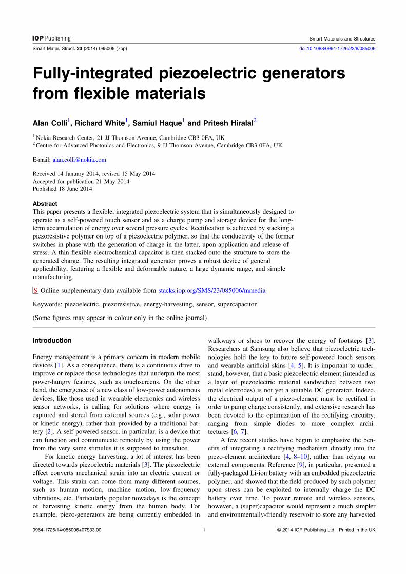
rectification is replaced by a pressure-controlled switch.Essentially, when pressure is applied on zone-II, the QTC™film resistance drops well below RS, and the charge inducedby the piezo-element is preferentially stored into the loadcapacitor CL. When the pressure is released though, theQTC™ film becomes an insulator, breaking the electricalconnection between CP and CL. Hence, the capacitor CP hasno other choice than to discharge through RS before anothercycle could begin. As a net result, a DC voltage VL developsacross the load.
An important condition must be fulfilled to validate thisidea. In figure 1(b), we emphasize that a QTC™ film sand-wiched between two planar electrodes has an intrinsic capa-citance CQTC. For efficient charge pumping, CQTC needs to bemuch smaller than CP. This is indeed the case for our device,since the measured values for CP and CQTC are 1.4 nF and15 pF, respectively.
According to the values chosen for the load and CL,different operational modes can be achieved. For example, ifthe device is supposed to work as a self-powered sensor todetect individual touch events, it is desirable to produce anoutput with the maximum voltage-per-pulse (i.e., reducing CL
to be on the same order of CP), and to fully discharge CL
before another event can occur (i.e., using a relatively smallload). Conversely, if one wants to slowly build up VL accu-mulating charge (and energy) into a CL≫CP over severalpressure cycles, then a relatively large load should be used toprevent the continuous and competing discharge of CL.
In figure 2 we investigate the first operational regime byapplying 5 N pressure pulses at a frequency of about 1 Hz.We choose RS = 100MΩ, CL = 10 nF and a load of 1MΩ.For a single pulse, the application and the release of pressureare separated by ∼200 ms. This is a realistic approximation ofthe action of tapping a finger. The simultaneous evolutions ofVL and VS are plotted in figure 2(a) for two pressure pulsesapplied to zone-I and zone-II. For zone-I pulses, since theQTC™ is in an insulating state at all times, VL is not affectedby the action. The measured VS closely reflects the typicalresponse of a piezo-element shorted through a resistor: avoltage peak (negative for this particular device) developsupon the application of pressure until CP is charged, then, asthe pressure is removed, the discharge of CP leads to acomplementary peak of positive voltage. If a pressure pulse isapplied to zone-II, however, the QTC™ film turns tempora-rily conductive, and the right branch of the circuit in figure 1is allowed to participate in the charging. Hence, a negative VL
peak develops in response to the application of pressure.Crucially, there is no positive VL peak as the pressure is lifted,because the QTC™ reverts to its insulating state and thedischarging occurs entirely through RS, similarly to zone-Ievents. This proves that the QTC™ is fast enough as apressure switch for effective rectification of the piezoelectricsignal. Note that the peak negative value measured for VS inzone-I is roughly 7× larger than the peak value for VL inzone-II. This VS/VL peak ratio follows the capacitance ratioCL/CP.
The reliability and reproducibility of all the above fea-tures are visible in figure 2(b), where both VL and VS are
plotted over a series of six consecutive pressure pulses, thefirst three applied on zone-II, the remaining ones on zone-I.Accordingly, if used as a touch sensor, this device wouldproduce a prompt, smooth, and consistent DC output for any‘press’ event on the active area (zone-II), irrespective of the
Figure 2. (a) Different evolution of VS and VL over a single pressurecycle (press + release) as stress is applied to zone-I or zone-II. VL isshifted by −2 V for clarity. (b) Evolution of VS and VL over multiplepressure cycles on different zones, showing the consistency of thesystem response. VS is shifted by 5 V for clarity.
3
Smart Mater. Struct. 23 (2014) 085006 A Colli et al

overall (and arbitrary) duration of individual touch events(i.e., how long the finger is kept down before release).
In figure 3 we use bigger values for CL and a load of1 GΩ to investigate the energy-harvesting and charge accu-mulation regime of our integrated piezo-generator. We apply5 N pressure pulses on zone-II at a rate of about 2 Hz until aVL of roughly 1 V is reached. Then, we let the system slowlydischarge according to its specific time constant (1 GΩ* CL).Unsurprisingly, the number of pulses needed to generateVL = 1 V (m) scales linearly with CL. For CL = 10 nF(figure 2), a single pulse was sufficient. Increasing CL to100 nF and 1 μF requires roughly 10 and 100 pulses,respectively (i.e., 5 and 50 s in figure 3). This allows us toeasily calculate the average charge per pulse that is pumpedinto CL, which turns out to be (1 V* CL)/m = 10−8 C.
Following the fundamental characterization above, wehave assembled a fully-packaged piezoelectric DC generatorby integrating both the RS resistor and the load capacitor CL
into a single flexible structure. Figure 4(a) schematicallyillustrates how the components are stacked and connected,while a picture of the physical prototype is shown infigure 4(b). We have used a narrow piece of carbon tape toconnect together the PVDF electrodes (RS∼ 40MΩ), andconductive copper tape for the metallic connections betweendifferent components. The load capacitor on the back of thestructure is a flexible supercapacitor (CL∼ 1 mF) fabricatedad-hoc (see experimental methods). It is obvious fromfigure 3 that this prototype requires a very large number ofpressure cycles (and a nominally infinite load under charging)to build up a significant VL. Since our supercapacitor alsoshowed a small leakage under bias, we could not achievesaturation values for VL larger than a few mV. It is thusimportant that the capacitor or supercapacitor, when needed,is carefully chosen to match the amount of charge supplied bythe piezoelectric pump in a defined regime of operation.
Discussion
We estimated above that the average charge that can bepumped per unit area in response of a fixed amount of pres-sure is about 2 nC N−1 cm−2. This is an acceptable value but,although it could be further improved by optimizing specifi-cations like the PVDF and the QTC™ thickness, it is unlikelyto match the most efficient piezoelectric generators to date,where crystals with higher piezoelectric coefficients are usedand rectification is achieved by more sophisticated circuitarchitectures [6, 7]. It is thus crucial to understand that themost important and unique benefits of our integrated piezo-generator device are essentially twofold: first, it is very robustand durable but at the same time very straightforward tofabricate; second, by providing a built-in solution for localrectification, it potentially allows the realization of very largearea devices with an efficient response to local stimuli, i.e.,devices that work well when the pressure is applied only on asmall fraction of the total area. We thus steer the followingdiscussion towards the evidence supporting these specificclaims.
Both the PVDF and the QTC™ components, takenindividually, have specifications as commercial products (seeExperimental Methods). PVDF is also extensively studied inapplied research, and its durability to stress cycles is mea-sured in the millions [16]. The QTC™ film as provided by
Figure 3. Charge accumulation regime for our piezoelectricgenerator. Higher values for CL allow more energy storage, but morepressure cycles are needed to achieve the same VL.
Figure 4. (a) Schematics and (b) photograph of a fully-integratedpiezoelectric generator made entirely from flexible materials.
4
Smart Mater. Struct. 23 (2014) 085006 A Colli et al
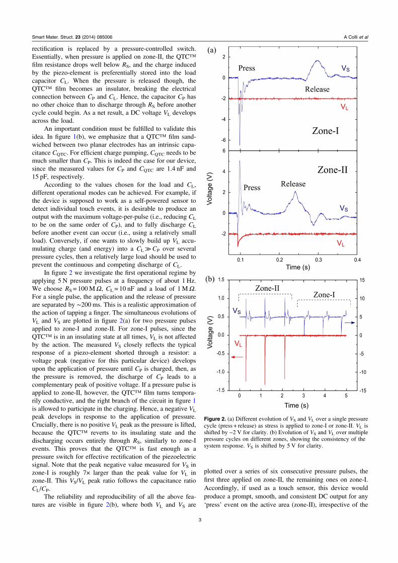
Peratech claims a lifetime of one million cycles for forces upto 50 Kg. Nevertheless, we have performed a simple 50 000cycles stress test for an integrated device similar to that stu-died in figure 2, more with the purpose of evaluating therobustness of the overall package than to confirm the dur-ability of its building blocks. The results reported in figure 5show that there is no visible degradation of the output signalVL after 50 000 cycles. This shows that our device concept isnot just based on durable materials, but also that long-termrobustness can be achieved by a cheap and straightforwardassembly strategy. This is crucial for some large area manu-facturing techniques like, e.g., roll-to-roll fabrication.
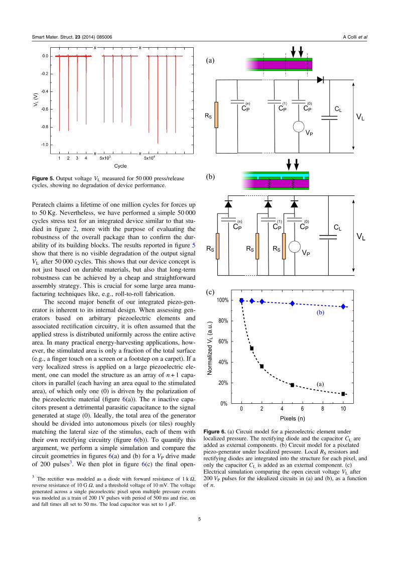
The second major benefit of our integrated piezo-gen-erator is inherent to its internal design. When assessing gen-erators based on arbitrary piezoelectric elements andassociated rectification circuitry, it is often assumed that theapplied stress is distributed uniformly across the entire activearea. In many practical energy-harvesting applications, how-ever, the stimulated area is only a fraction of the total surface(e.g., a finger touch on a screen or a footstep on a carpet). If avery localized stress is applied on a large piezoelectric ele-ment, one can model the structure as an array of n+ 1 capa-citors in parallel (each having an area equal to the stimulatedarea), of which only one (0) is driven by the polarization ofthe piezoelectric material (figure 6(a)). The n inactive capa-citors present a detrimental parasitic capacitance to the signalgenerated at stage (0). Ideally, the total area of the generatorshould be divided into autonomous pixels (or tiles) roughlymatching the lateral size of the stimulus, each of them withtheir own rectifying circuitry (figure 6(b)). To quantify thisargument, we perform a simple simulation and compare thecircuit geometries in figures 6(a) and (b) for a VP drive madeof 200 pulses3. We then plot in figure 6(c) the final open-
Figure 5. Output voltage VL measured for 50 000 press/releasecycles, showing no degradation of device performance.
Figure 6. (a) Circuit model for a piezoelectric element underlocalized pressure. The rectifying diode and the capacitor CL areadded as external components. (b) Circuit model for a pixelatedpiezo-generator under localized pressure. Local RS resistors andrectifying diodes are integrated into the structure for each pixel, andonly the capacitor CL is added as an external component. (c)Electrical simulation comparing the open circuit voltage VL after200 VP pulses for the idealized circuits in (a) and (b), as a functionof n.
3 The rectifier was modeled as a diode with forward resistance of 1 k Ω,reverse resistance of 10 G Ω, and a threshold voltage of 10 mV. The voltagegenerated across a single piezoelectric pixel upon multiple pressure eventswas modeled as a train of 200 1V pulses with period of 500 ms and rise, onand fall times all set to 50 ms. The load capacitor was set to 1 μF.
5
Smart Mater. Struct. 23 (2014) 085006 A Colli et al
circuit voltage VL as a function of n, normalized to thatobtained in the case of a single device or pixel (n= 0). Thesimulation confirms that, for the circuit modeled infigure 6(a), the output voltage VL decays rapidly with thenumber of pixels. Conversely, for the circuit in figure 6(b),the output shows only a very weak dependence on the numberof pixels.
The message conveyed by figure 6 is of general validity.Even if the simulation is not tailored to our particular com-ponents (in fact, a conventional diode is not a good approx-imation for our QTC™ ‘rectifier’), it sets down therequirements for the optimal architecture. For our devicespecifically, it is crucial to maximize the voltage output of asingle pixel. Replacing a conventional diode with a pressureswitch means that, if the stimulus voltage is not larger thanthe voltage already built into CL, not only charge pumpingdoes not occur, but some current can actually flow back fromCL towards the piezo-elements. The small drawing associatedto figure 6(b) shows our proposed approach to turn a singleintegrated piezo-generator into a pixelated structure thatmimics the optimal circuit geometry. One has only to patternthe metallic electrode on top of the piezoelectric materialaccording to the expected stimulus area, and provide indivi-dual RS connections to the bottom electrode. If the piezo-electric material itself has (or is engineered to have) aninternal resistance within the suitable RS tolerance (fairlywide, see supporting information), the implementation isstraightforward. Note that there is no need to pattern thepiezoresistive material, as this becomes locally conductiveonly where pressure is applied. For energy-harvesting appli-cations, where the collective output of all pixels is funneledinto a single capacitor (or battery) as in figure 6(b), there is noneed to pattern the uppermost metal electrode either (becausestill CQTC≪CP). On the other hand, if the pressure stimulusneeds to be spatially resolved (e.g., for touchscreen applica-tions), the uppermost metal electrode needs to be patternedinto pixels that mirror those of the metallic electrode below.Such pixels must then be wired out independently by meansof, e.g., a crossbar architecture.
It is worth comparing our technology and relatedimplementations to the DC piezo-generator proposed byWang’s group [8] and further exploited in [4, 5]. Theirapproach based on vertically-aligned ZnO nanowires isingenious: according to our understanding, each individualZnO nanowire provides a piezoelectric drive via mechanicalbending, a resistor RS through itself (n-type ZnO is a poorconductor but not an insulator), and the equivalent of a rec-tifying diode via a mechanical ohmic/Schottky-contact switchat its tip. It is thus an alternative and feasible implementationof the optimal circuit geometry shown in figure 6(b). How-ever, by the authors’ own admission, there were problemswith the output stability, mechanical robustness, lifetime andenvironmental adaptability of such devices, which eventuallypushed them towards planar nanowire geometries [17, 18], orvertically-aligned nanowire arrays supported by a soft poly-mer matrix [18, 19]. However, as nanowires are clamped atboth sides with either an ohmic or Schottky contact [17–19],the rectification mechanism exploited in [8] is lost. The
PVDF-based piezo-electrochemical cell demonstrated in [9],on the other hand, preserves the rectification feature andseems to show better robustness, but it still faces the chal-lenge of growing vertically-aligned TiO2 nanotubes overlarge areas coupled with the need of sealing the LiPF6 elec-trolyte in a solid and safe packaging. Moreover, it is mostlyoriented to energy-harvesting and not truly optimized forsensing applications like touchscreens. Overall, our deviceshave an efficiency on par with [9], are very robust and dur-able, are much easier to fabricate, and are much more scalabletoward very large areas, which makes them suitable for awider range of applications.
Conclusions
As concluding remarks, we highlight a few additional pointsof practical interest. First, our technology is applicable to anypiezoelectric material, hard or soft. For flexible and deform-able devices, PVDF is ideal as it produces a larger outputwhen allowed to bend under pressure [20]. Second, the wholeintegrated structure can in principle be made transparent, acompulsory feature for touchscreen applications. Indeed,transparent piezoelectric materials are common (quartz orPVDF), transparent electrodes can be made of ITO or gra-phene [21], and the piezoresistive QTC™ film is also avail-able in a transparent form [11]. Transparent supercapacitorsare also available, if needed [22, 23]. Finally, given therelatively thin-film nature of all layers involved, it is possibleto stack many integrated piezo-generators together to max-imize the energy harvested from a single stimulus. Aftertaking all data and arguments into account, we believe thatour integrated piezoelectric system possesses enough meritsto suggest great potential as a viable commercial technol-ogy [24].
Acknowledgements
We thank G A J Amaratunga for useful discussion. We thankMeasurement Specialties and Peratech for supplying us withthe PVDF element and the QTC™ element, respectively.
References
[1] Rouvala M, Amaratunga G A J, Wei D and Colli A 2010Nanotechnologies for Future Mobile Devices ed T Ryhanen,M A Uusitalo, O Ikkala and A Karkkainen (Cambridge, UK:Cambridge University Press) chapter 3
[2] Beeby S and White N 2010 Energy Harvesting forAutonomous Systems (Boston, MA: Artech House)
[3] Kim H S, Kim J-H and Kim J 2011 Int. J. Precis. Eng. Man.12 1129
[4] Choi M-Y, Choi D, Jin M-J, Kim I, Kim S-H, Choi J-Y,Lee S Y, Kim J M and Kim S-W 2009 Adv. Mater. 21 2185
[5] Choi D et al 2010 Adv. Mater. 22 2187[6] Ramadass Y K and Chandrakasan A P 2010 IEEE J. Solid-
State Circuits 45 189
6
Smart Mater. Struct. 23 (2014) 085006 A Colli et al

[7] Han J, von Jouanne A, Le T, Mayaram K and Fiez T S 200419th Annu. IEEE Applied Power Electronics Conf. andExposition vol 3 p 1541
[8] Wang X, Song J, Liu J and Wang Z L 2007 Science 316 102[9] Xue X, Wang S, Guo W, Zhang Y and Wang Z L 2012 Nano
Lett. 12 5048[10] McKay T G, O’Brien B M, Calius E P and Anderson I A 2011
Appl. Phys. Lett. 98 142903[11] Peratech Ltd 1998 UK Patent PCT/GB98/00206 (WO 98/33193)[12] Bloor D, Donnelly K, Hands P J, Laughlin P and Lussey D
2005 J. Phys. D: Appl. Phys. 38 2851[13] Bloor D, Graham A, Williams E J, Laughlin P J and Lussey D
2006 Appl. Phys. Lett. 88 102103[14] Gamby J, Taberna P L, Simon P, Fauvarque J F and
Chesneau M 2001 J. Power Sources 101 109[15] Stoller M D, Park S, Zhu Y, An J and Ruoff R S 2008 Nano
Lett. 8 3498
[16] Shirinov A V and Schomburg W K 2008 Sensors Actuators A142 48
[17] Yang R, Qin Y, Dai L and Wang Z L 2009 Nat. Nanotechnol.4 34
[18] Xu S, Qin Y, Xu C, Wei Y, Yang R and Wang Z L 2010 Nat.Nanotechnol. 5 366
[19] Momeni K, Odegard G M and Yassara R S 2010 J. Appl. Phys.108 114303
[20] Mateu L and Moll F 2005 J. Intell. Mater. Syst. Struct. 16 835[21] Bonaccorso F, Sun Z, Hasan T and Ferrari A C 2010 Nat.
Photon. 4 611[22] Chen P-C, Shen G, Sukcharoenchoke S and Zhou C 2009
Appl. Phys. Lett. 94 043113[23] Hiralal P, Wang H, Unalan H E, Liu Y, Rouvala M, Wei D,
Andrew P and Amaratunga G A J 2011 J. Mater. Chem. 2117810
[24] Colli A and White R 2014 Patent pending
7
Smart Mater. Struct. 23 (2014) 085006 A Colli et al