full chip characterization of compression algorithms for direct
TRANSCRIPT
Full Chip Characterization of CompressionAlgorithms for Direct Write Maskless
Lithography SystemsAvideh Zakhor, Vito Dai, and George Cramer
University of California, Berkeley
Abstract
Future lithography systems must produce more dense microchips with smaller feature sizes, while maintaining through-put comparable to today’s optical lithography systems. This places stringent data-handling requirements on the design ofany maskless lithography system. Today’s optical lithography systems transfer one layer of data from the mask to the entirewafer in about sixty seconds. To achieve a similar throughput for a direct-write maskless lithography system with a pixelsize of 22 nm, data rates of about 12 Tb/s are required. Over the past 8 years, we have proposed a datapath architecturefor delivering such a data rate to a parallel array of writers. Our proposed system achieves this data rate contingent ontwo assumptions: consistent 10 to 1 compression of lithography data, and implementation of real-time hardware decoder,fabricated on a microchip together with a massively parallel array of lithography writers, capable of decoding 12 Tb/s ofdata.
To address the compression efficiency problem, in the past few years, we have developed a new technique, ContextCopy Combinatorial Coding (C4), designed specifically for microchip layer images, with a low-complexity decoder forapplication to the datapath architecture. C4 combines the advantages of JBIG and ZIP, to achieve compression ratios higherthan existing techniques. We have also devised Block C4, a variation of C4 with up to hundred times faster encodingtimes, with little or no loss in compression efficiency. While our past work has focused on characterizing the compressionefficiency of C4 and Block C4 on samples of a variety of industrial layouts, there has been no full chip performancecharacterization of these algorithms. In this paper, we show compression efficiency results of Block C4 and competingtechniques such as BZIP2 and ZIP for the Poly, Active, Contact, Metal1, Via1, and Metal2 layers of a complete industry65 nm layout.
Overall, we have found that compression efficiency varies significantly from design to design, from layer to layer,and even within parts of the same layer. It is difficult, if notimpossible, to guarantee a lossless 10 to 1 compression forall blocks within a layer, as desired in the design of our datapath architecture. Nonetheless, on the most complex Metal1layer of our 65 nm full chip microprocessor design, we show that a average lossless compression of 5.2 is attainable,which corresponds to a throughput of 60 wafer layers per hourfor a 1.33 Tb/s board-to-chip communications link. Asa reference, state-of-the-art HyperTransport 3.0 offers 0.32 Tb/s per link. These numbers demonstrate the role losslesscompression can play in the design of a maskless lithographydatapath.
I. I NTRODUCTION
Future lithography systems must produce chips with smallerfeature sizes, while maintaining throughput comparableto today’s optical lithography systems. This places stringent data handling requirements on the design of any direct-writemaskless system. Optical projection systems use a mask to project the entire chip pattern in one flash. An entire wafercan then be written in a few hundreds of such flashes. To be competitive with today’s optical lithography systems,direct write maskless lithography needs to achieve throughput of one wafer layer per minute. In addition, to achievethe required 1 nm edge placement with 22 nm pixels in 45 nm technology, a 5-bit per pixel data representation isneeded. Combining these together, the data rate requirement for a maskless lithography system is about 12 Tb/s. Toachieve such a data rate, we have recently proposed a data path architecture shown in Figure 1 [4], [2], [1], [34]. Inthis architecture, rasterized, flattened layouts of an integrated circuit (IC) are compressed and stored in a mass storagesystem. The compressed layouts are then transferred to the processor board with enough memory to store one layer ata time. This board will then transfer the compressed layout to the writer chip, composed of a large number of decodersand actual writing elements. The outputs of the decoders correspond to uncompressed layout data and are fed into D/Aconverters driving the writing elements such as a micro-mirror array or E-beam writers.
In the proposed data-delivery path, compression is needed to minimize the transfer rate between the processor boardand the writer chip, and also to minimize the required disk space to store the layout. Since there are a large numberof decoders operating in parallel on the writer chip, an important requirement for any compression algorithm is to

Decoder-Writer Chip
Processor Board 64 GBit DRAM
1.2 Tb/s
Decoder
10 to 1 single compressed layer
Storage Disks 640 GBit
12 Tb/s
10 to 1 all compressed layers
1.1 Gb/s
Writers
Fig. 1. System architecture of a data-delivery system for maskless lithography.
TABLE I
SPECIFICATIONS FOR AN INDUSTRY MICROPROCESSOR DESIGNED FORTHE 65NM DEVICE GENERATION.
Manufacturing specifications Maskless lithography specificationsMinimum feature 65 nm Pixel size 32 nmEdge placement 1 nm Pixel depth 6 bits (0-32) grayChip size 8.3 mm× 14.1 mm Pixel data 689 Gb
(one chip layer)Wafer size 300 mm Wafer data 415 Tb
(one wafer layer)Wafer throughput 1 wafer per 60s Average data 6.9 Tb/s over(one layer) throughput one wafer layer
have an extremely low decoder complexity. To this end, we have proposed a lossless layout compression algorithmfor flattened, rasterized data called Context Copy Combinatorial Coding (C4) which has been shown to outperformall existing techniques such as BZIP2, 2D-LZ, and LZ77 in terms of compression efficiency, especially under limiteddecoder buffer size, as required for hardware implementation[1]. We have also devised Block C4, a variant of C4, withup to hundred times faster encoding times, with little or no loss in compression efficiency[34].
While our past work has focused on characterizing the compression efficiency of C4 and Block C4 on samples of avariety of industrial layouts, there has been no full chip performance characterization of these algorithms. In this paper,we show compression efficiency results of Block C4 and competing techniques such as BZIP2 and ZIP for the Poly,Active, Contact, Metal1, Via1, and Metal2 layers of a complete industry 65 nm layout. Specifically, we re-examine thecomparison between Block C4, ZIP, and BZIP2, only this time,statistics are presented for a full production industrymicroprocessing chip, rather than individual images sampled here and there across a chip.
The layout used for these calculations are for an industry standard microprocessor designed for the 65nm devicegeneration. The specifications for manufacturing this design is shown in Table I. The layout is8.3mm × 14.1mm insize with polygons laid out on a 1nm grid. The appropriate pixel size for this generation is32nm×32nm, with 33 (0-32)levels of gray to achieve 1nm edge placement control, which requires 6-bits per pixel. The computed rasterized pixelimage data is 0.7 Tb per chip layer, 415 Tb per wafer layer. Themanufacturing throughput requirement for lithographyis 1 wafer layer per 60s. Therefore, the required average maskless lithography data rate over one wafer layer is 6.9Tb/s.
In previous work, individual layout clips are characterized as dense, sparse, repetitive, and non-repetitive, with eachterm intuitively defined by visual inspection. This manual ad hoc characterization does not scale to a full chip run.Instead, we define here a metric for polygon complexity whichintuitively matches to the concept of “dense”, namelythe number of polygon vertices within a given area, orvertex density. If the number of vertices is large in a fixed area,then it must be caused by either the presence of many distinctpolygons, or polygons with very complex fragmentededges. In either case, for the simple 3-pixel prediction mechanism used by C4 and BlockC4, the number of vertices isdirectly correlated with the number of context-based prediction errors.
In terms of repetitions, it is difficult to find a single metricthat decisively determines this for a 2D image and that isreasonable to compute for such a large data set. One method would have been to use the same search based segmentation

Fig. 2. A vertex density plot of Metal1 layer for a 65nm microprocessor.
used by LZ77/C4 itself, but this defeats the purpose of having an independent metric. Other techniques evaluated, suchas image correlation and window-based Discrete Cosine Transform, do not correlate well with the copy mechanism ofC4 and LZ77 for which the cost of even correcting a small 1% intensity error is fairly high. Such techniques are moreappropriate for lossy compression techniques where such errors may be ignored. In the end, we choose to use a metrictaken from the layout hierarchy itself. The measure of repetition is defined as the number of cells in a given region,minus the number of unique cells in that same region. As an example, suppose a region contains 5 instances of cell A, 4instances of cell B, and 1 instance of C, D, and E. Then the total number of cells in that region is5+4+1+1+1 = 12whereas the total number of unique cells is 5 (A-E), so the “repetition” of this region is 7.
In order to provide a visualization of the these metrics, Figure 2 shows a grayscale picture of the vertex densitymetric as applied to the Metal 1 layer. Each pixel in this picture corresponds to a32µm × 32µm block of the chip.Vertex densities range from 0 to 20,000 per block. Higher vertex density blocks are assigned brighter pixels, and lowercorner vertex density blocks are assigned darker pixels. Itis easy to discern from this image regions of very high vertexdensities that are arranged in rectangular arrays throughout the design. These are the various memory arrays of themicroprocessor. The darker grays are likely to be logic circuit areas, also arranged in rectangular arrays. Finally, theperiphery regions are very dark, indicating low corner densities.
A plot of “repetitions” visually looks the same as Figure 2. Although there are small differences in the data whichare detectable through data analysis, it is impossible to visually discern these differences. The visual similarity betweena plot of “repetitions” and a plot of vertex density justifiesthe fundamental rationale behind C4. Highly dense layoutregions are also highly repetitive, and therefore compresswell with copying techniques. Non-repetitive regions tendtobe sparse, and hence compress well with context based prediction techniques, as polygon corners generally correspondto prediction errors for Manhattan geometries.
For each of the32µm× 32µm blocks, rasterization is performed using the methodology described in [42], where thepixel size is 32nm, and 33 gray levels are allowed (0-32) resulting in a fine 1nm edge placement grid. One full chip layercontains 116,328 such blocks, equal to the number of pixels in Figure 2. Each rasterized block is then passed through3 compression algorithms, ZIP, BZIP2, and Block C4 and compression and decompression statistics are gathered for

TABLE II
FULL -CHIP COMPRESSION SUMMARY TABLE.
Statistic Layer ZIP BZIP2 Block C4Avg. Compression Ratio Poly 12.6 15.3 14.1
Metal1 4.2 4.5 5.2Metal2 6.1 7.2 7.2Contact 14.1 16.0 23.2Active 20.2 31.7 39.2Via1 12.3 14.1 14.0
Min. Compression Ratio Poly 2.6 3.1 4.4Metal1 0.96 1.3 1.7Metal2 1.0 1.3 2.1Contact 2.7 4.3 4.8Active 8.1 11.1 12.8Via1 2.2 3.6 4.5
Total Encoding Time Poly 42 min 2.3hrs 420 hrsMetal1 45 min 2.3hrs 420 hrsMetal2 45 min 1.9hrs 408 hrsContact 46 min 2.1hrs 419 hrsActive 43 min 1.9hrs 418 hrsVia1 46 min 2.1hrs 419 hrs
Total Decoding Time Poly 17 min 1.2hrs 36 minMetal1 14 min 1.2hrs 35 minMetal2 19 min 1.4hrs 38 minContact 15 min 1.4hrs 38 minActive 15 min 1.3hrs 37 minVia 15 min 1.4hrs 38 min
Percentage of Blocks Poly 25.33% 22.84% 23.66%with Compression Metal1 65.73% 59.69% 55.12%Ratio Below 10 Metal2 44.20% 44.88% 41.95%(lower is better) Contact 0.73% 0.07% 0.00%
Active 7.85% 0.00% 0.00%Via 4.94% 0.22% 0.14%
each. This process is then repeated for all the critical layers of the design: diffusion, also known as active, poly, contact,metal1, via1 and metal2.
For this experiment, decoder buffer size of ZIP, BZIP2 and Block C4 are 4kB, 900 kB, and 1.7 kB respectively,chosen based on the tradeoff analysis presented in [34]. Thesmall buffer size used by Block C4 makes it particularlyattractive for implementation in hardware for the datapatharchitecture presented earlier.
II. FULL CHIP COMPRESSION STATISTICS
Table II contains a summary of these full chip runs. Column 1 is the name of the full-chip statistic being reported.Column 2 is the chip layer which is rasterized and compressed. Columns 3, 4, and 5 are the statistics for ZIP, BZIP2and Block C4 respectively. Each row in the table represents alayer statistic. The relevant statistics reported are theaverage compression ratio for the entire layer, the minimumcompression ratio over individual32µm × 32µm blocks,the total encoding run time for each layer, the total decoding run time for each layer, and the percentage of blocks withcompression ratio below 10.
Examining the average compression ratio for all layers, thecompression efficiency of ZIP is generally lower thanthat of BZIP2 and Block C4. BZIP2 and Block C4 are generally comparable to each other. Considering that BlockC4uses 2 or 3 orders of magnitude less decoder buffer to achievemore or less the same compression efficiency as BZIP2,clearly it is the algorithm of choice for hardware implementation. From layer to layer, Metal1 is most challenging
to compress, followed by Metal2, Via1, Poly, Contact, then Active. One different characteristic of Poly layout in thisparticular design style is that all gates are oriented in a single direction, and are spaced apart by a characteristic commonpitch. Regularized design styles such as these can take better advantage of the copy mechanism in C4 to achieve highcompression efficiency. Of particular concern is the average compression ratio of the Metal1 and Metal2 layers whichare 5.2 and 7.2 respectively, which fall below the target compression ratio of 10.
Another important metric to consider is the minimum compression ratio over all32µm×32µm blocks for a layer. Thisis the most difficult block of any given layer to compress. In this case, only the Active layer meets a target compressionratio of 10. The remaining 5 layers fall below that target, and in the worst case block of Metal1, the compression ratiois 1.7.
III. M ANAGING LOCAL VARIATIONS IN COMPRESSION RATIOS
So what are the implications of missing the compression target, and which is more relevant, the average compressionratio, or the more pessimistic minimum compression ratio? The answer depends on how well the maskless lithographysystem as a whole can absorblocal variations in data throughput. This can be accomplished by physically varying thethroughput of the maskless lithography writers, or by introducing various mechanisms in the datapath to absorb thesevariations which we will speculate on later. Bylocal variations, we are referring to inter-block variations of compressionratios. In choosing our block size for analysis, we already assume there is at least a single block buffer in the systemso that we may ignore intra-block variations in compressionratio. This buffer is distinct from the memory used by thedecompression hardware. An example of such a buffer is the “SRAM Writer Interface” found in [39].
A. Adjusting board to chip communication throughput
In the worst case, (a) the maskless lithography writers are fixed at a constant writing speed over all blocks of a layer;and (b) the datapath cannot help absorb these inter-block variations of compression ratios. In this case, the writing speedis limited by the data throughput of the minimum compressionratio block. From the the maskless datapath presentedearlier, the formula to compute actual wafer throughput isrwafer = rcomm,max × Cmin/dwafer whererwafer is thewafer layer throughput,rcomm,max is the maximum board to chip communication throughput,Cmin is the minimumcompression ratio for Block C4, anddwafer = 415 Tb is the total data for one wafer layer, from Table I.
Sincedwafer is fixed andCmin has been empirically determined for each layer, the total wafer throughput dependsentirely onrcomm,max which is themaximum data throughput of board to chip communication. The reason maximumis emphasized is that this throughput is only required for the minimum compression ratio block. For blocks ofhigher compression ratio, the communication throughput can be reduced. As an example, if maximum communicationthroughputrcomm,max = 1 Tb/s, then the wafer layer throughput for Metal1 is 1 Tb/s× 1.7 / 415 Tb× 3600s/hr =14.7 wafer layers per hour. This same formula can be applied to each layer for various assumed values ofrcomm,max.The results of this exercise are shown in the third and forth column of Table III.
The first four columns of Table III are layer, minimum compression ratio, maximum board to chip communicationthroughput, and wafer layer throughput, respectively. In the first 6 rows, we assume a maximum communicationthroughput of 1 Tb/s and compute the wafer throughput for various layers. In the next 6 rows, we target a waferthroughput of 60 wafer layers per hour, and compute the maximum communication throughput needed to supportthis writing rate for each layer. As a point of reference, a state-of-the-art HyperTransport 3.0 (HT3) link offers 0.32Tb/s maximum throughput [40]. Examining the third column ofTable III for Metal1 with a target wafer throughputof 60 wafers per hour, a maskless datapath requires at leastd4.07/0.32e = 13 such links to achieve the requiredcommunications throughput. Implementing 13 links is costly, in terms of both circuit power dissipation and chip area[34] [23]. However, a chip designer may be able to conserve power by taking advantage of the fact that the maximumcommunication throughput is only needed for a few blocks. The average communication throughput, as we shall seeshortly, is significantly lower.
The equation relating wafer throughputrwafer to average board to chip communication throughputrcomm,avg andaverage compression ratioCavg is straightforward:rwafer = rcomm,avg × Cavg/dwafer. To be precise, the average iscomputed over all blocks of an wafer layer. Using this formula, we can relate wafer throughput to average communicationthroughput for various layers. The results are presented inthe last three columns of Table III. The columns are averagecompression ratio, average board to chip communication throughput, and wafer layer throughput, respectively. The first6 rows assume an average communications throughput of 1 Tb/s, and the next 6 rows target a wafer throughput of 60wafer layers per hour.

TABLE III
MAXIMUM COMMUNICATION THROUGHPUT VS. WAFER LAYER THROUGHPUT FOR VARIOUS LAYERS IN THE WORST CASE SCENARIO, WHEN
DATA THROUGHPUT IS LIMITED BY THE MINIMUM COMPRESSION RATIOFOR BLOCK C4.
Layer Cmin rcomm,max rwafer Cavg rcomm,avg rwafer
(Tb/s) (wafer · layer/hr) Tb/s (wafer · layer/hr)Poly 4.4 1 38.2 14.1 1 122Metal1 1.7 1 14.7 5.2 1 45.1Metal2 2.1 1 18.2 7.2 1 62.5Contact 4.8 1 41.6 23.2 1 201Active 12.8 1 111 39.2 1 340Via1 4.5 1 39.0 14.0 1 121
Poly 4.4 1.57 60 14.1 0.49 60Metal1 1.7 4.07 60 5.2 1.33 60Metal2 2.1 3.29 60 7.2 0.96 60Contact 4.8 1.44 60 23.2 0.30 60Active 12.8 0.54 60 39.2 0.18 60Via1 4.5 1.54 60 14.0 0.49 60
Since the average compression ratio is significantly higherthan the minimum compression ratio for all layers, theaverage communication throughput is also significantly lower than the maximum communication throughput computedpreviously. Continuing our previous example using a HT3 link as reference, for Metal1 with a target wafer throughputof 60 wafers per hour, a maskless datapath requires only1.33/0.32 = 4.2 links on average. So even though 13 linksare required to accommodate the maximum throughput, on average only4.2/13 = 32% of the capacity is being used.The maskless datapath can take advantage of this by poweringdown unused communication links to conserve power.However, that still leaves an area cost of implementing 13 links in the first place. What can be done to effectivelysmooth the data throughput so that communication links can be utilized more effectively?
B. Statistical multiplexing using parallel decoders
An important feature to take advantage of is the opportunityto utilize averaging inherent in the parallel designof the maskless lithography datapath. As described in [41],the decoder in Figure 1 is implemented as a parallelarray of decoder paths, i.e. multiple blocks are being decoded simultaneously. In its simplest form, the communicationthroughput is evenly divided among the parallel decoder paths. However, additional logic, such as packet scheduling,can be implemented to allocate communication throughput toeach decoder path based on need. As such, a decoder pathworking on a block with low compression ratio is allocated more communication packets than a decoder path workingon a block with high compression ratio. The result is that inter-block variations in compression ratio are effectivelystatistically multiplexed by the number of decoder paths inthe system.
Suppose we have N decoder paths working in parallel on N adjacent blocks in a row. In communication order, weform M frames of N blocks per frame, whereMN ≥ 116, 326. Statistical multiplexing effectively allows us to averagethe compression ratio over each frame. We can then compute the minimum over all frames and denote this value asCmin,N . Note, that by definitionCmin,1 = Cmin andCmin,116,328 = Cavg. Cmin,N , rwafer andrcomm,max are relatedthrough this equation:rwafer = rcomm,max × Cmin,N/dwafer.
Using different values for N, we compute theCmin,N andrcomm,max for Block C4, Metal1, and a target throughputof 60 wafer layers per hour. These results are summarized in Table IV. In columns are the number of decoder paths N,the minimum frame compression ratioCmin,N , the maximum board to chip communications throughputrcomm,max,the wafer throughputrwafer, and the number of HT3 links needed to support the communications throughput. Clearly,Cmin,N increases as the number of decoder paths N increases. AtN = 1000, Cmin,N = 4.9 which is very closeto Cavg = 5.2, demonstrating the strength of the statistical multiplexing approach. The corresponding maximumcommunication throughput is 1.41 Tb/s which can be met withd1.41/0.32e = 5 HT3 links.
TABLE IV
EFFECT OF STATISTICAL MULTIPLEXING USINGN PARALLEL DECODER PATHS ONBLOCK C4 COMPRESSION RATIO AND COMMUNICATION
THROUGHPUT FORMETAL1.
N Cmin,N rcomm,max(Tb/s) rwafer(wafer · layer/hr) # of HT3 links1 1.7 4.07 60 132 2.3 3.01 60 1010 2.5 2.77 60 9100 3.3 2.10 60 71000 4.9 1.41 60 5116,328 5.2 1.33 60 5
C. Adding buffering to the datapath
Another way to smooth the data throughput is to introduce on-chip memory buffer at the output of the communicationschannel before decompressing the data in Figure 1. This buffer absorbs variations in data throughput caused by inter-block variations of compression ratios. For blocks with high compression ratios, excess communication throughputis used to fill the buffer. For blocks with low compression ratio, data is drained from the buffer to supplement thecommunication channel. Intuitively, the larger the bufferis, the more variations it can absorb, and the lower is therequired maximum communication throughput. On the other hand, the primary advantage of spending area on a bufferin the first place is to save on chip area devoted to communication. Therefore, there is a tradeoff between the areaneeded by the buffer and the additional area saved by reducing the number of communication links.
We can roughly estimate the amount of buffer to add using the following steps. Suppose we add sufficient bufferequivalent to the minimum compressed block. For Metal1, this buffer is(1000 × 1000 × 6bits)/1.7 = 3.5Mb in sizefor Block C4. Now suppose, in communication order, we group blocks pairwise and compute each pair’s compressionratio, followed by computing the minimum over all pairsCmin,pair . This number is guaranteed to be higher thanCmin
and lower thanCavg . Empirically for Metal1,Cmin,pair = 2.3 for Block C4, assuming raster scan order. For thissystem, the following inequality holds:rwafer ≥ rcomm,max × Cmin,pair/dwafer. That is, at the very least, we shouldbe able to replaceCmin with the higherCmin,pair for relating wafer throughput to the maximum communicationthroughput. Continuing our previous example for Metal1 with a target wafer throughput of 60 wafers per hour, theresult isrcomm,max ≤ 3.01Tb/s, equivalent tod3.01/0.32e = 10 HT3 links. Compared with the 13 HT3 links for zerobuffering, this is a reduction of 3 links for 3.5Mb of buffering, which seems to be worthwhile tradeoff. Clearly, moresystematic analysis of such tradeoffs are necessary for anyfuture practical maskless lithography systems.
D. Distribution of low compression blocks
The computation ofrcomm,max in the previous paragraph is a conservative upper bound, in that it focuses on theworst case where low compression ratio blocks may be clustered together. Thus, we require that any drain on the buffercaused by a low compression ratio block to be immediately refilled by the adjacent block. If low compression blocksare spread far apart from each other by coincidence, thenrcomm,max may be significantly lowered. Furthermore, ifthe writing system allows for limited re-ordering of the blocks, then this could be used to intentionally spread the lowcompression ratio blocks apart. As an example, some maskless lithography systems are written in a step-and-scan mode,where multiple blocks form a frame which is written in a single scan [41]. In this case, blocks may be re-ordered withina frame to smooth the data rate.
Figure 3 is a visualization of the compression ratio distribution of Block C4 for the Metal1 layer. Brighter pixels areblocks with low compression ratios and darker pixels are blocks with high compression ratios. Notice that repetitivememory arrays on the bottom half are relatively dim. Block C4compresses these repetitive regions effectively. The lessregular, but relatively dense layout are clustered in distinct bright regions in the middle. This geographic distributionshould be taken into consideration when deciding on the mechanism to smooth inter-block variations.
E. Modulating the writing speed
Another possibility is to modulate the writing speed of the maskless lithography writers to match the inter-blockvariations in compression ratio. For example, it is conceivable to divide blocks into discrete classes based on the range
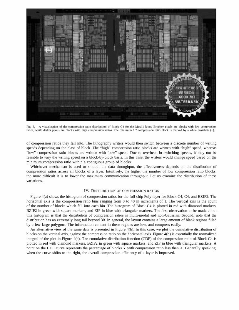
Fig. 3. A visualization of the compression ratio distribution of Block C4 for the Metal1 layer. Brighter pixels are blocks with low compressionratios, while darker pixels are blocks with high compression ratios. The minimum 1.7 compression ratio block is marked by a white crosshair (+).
of compression ratios they fall into. The lithography writers would then switch between a discrete number of writingspeeds depending on the class of block. The “high” compression ratio blocks are written with “high” speed, whereas“low” compression ratio blocks are written with “low” speed. Due to overhead in switching speeds, it may not befeasible to vary the writing speed on a block-by-block basis. In this case, the writers would change speed based on theminimum compression ratio within a contiguous group of blocks.
Whichever mechanism is used to smooth the data throughput, the effectiveness depends on the distribution ofcompression ratios across all blocks of a layer. Intuitively, the higher the number of low compression ratio blocks,the more difficult it is to lower the maximum communication throughput. Let us examine the distribution of thesevariations.
IV. D ISTRIBUTION OF COMPRESSION RATIOS
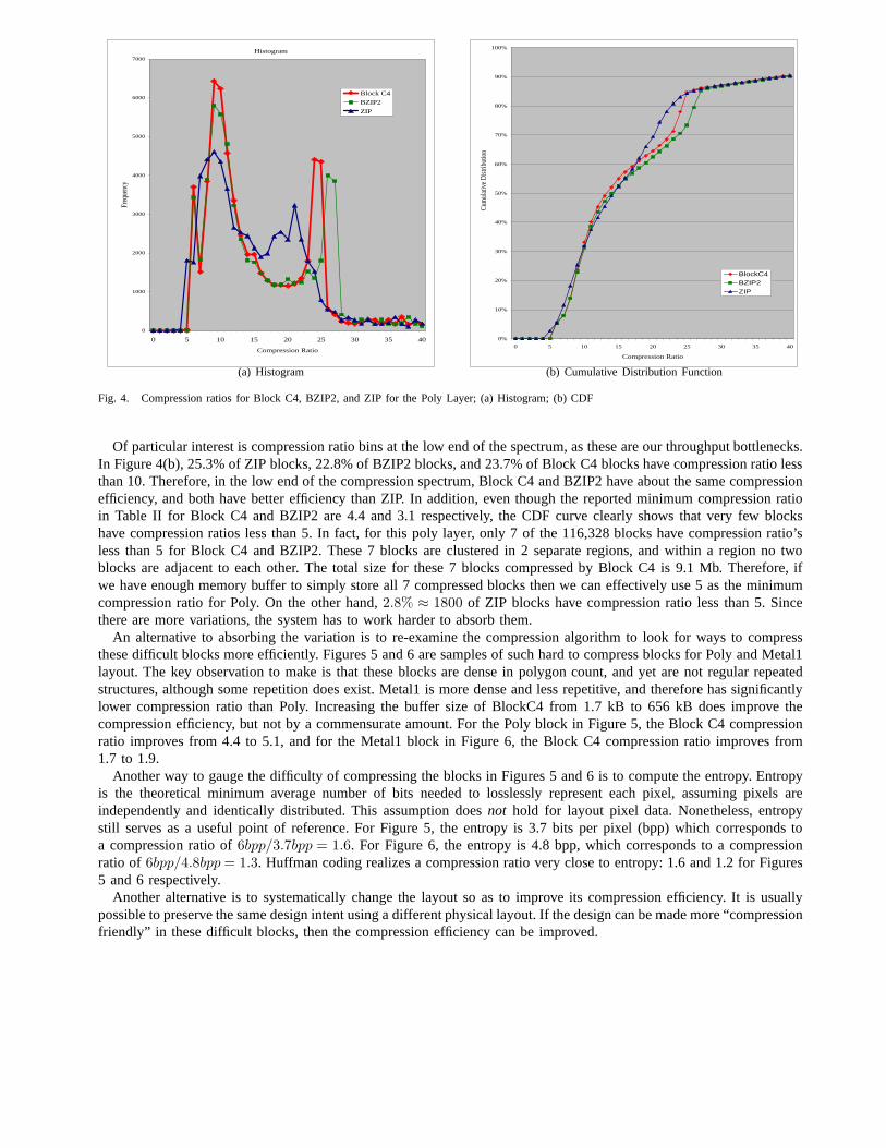
Figure 4(a) shows the histogram of compression ratios for the full-chip Poly layer for Block C4, C4, and BZIP2. Thehorizontal axis is the compression ratio bins ranging from 0to 40 in increments of 1. The vertical axis is the countof the number of blocks which fall into each bin. The histogram of Block C4 is plotted in red with diamond markers,BZIP2 in green with square markers, and ZIP in blue with triangular markers. The first observation to be made aboutthis histogram is that the distribution of compression ratios is multi-modal and non-Gaussian. Second, note that thedistribution has an extremely long tail beyond 30. In general, the layout contains a large amount of blank regions filledby a few large polygons. The information content in these regions are low, and compress easily.
An alternative view of the same data is presented in Figure 4(b). In this case, we plot the cumulative distribution ofblocks on the vertical axis, against the compression ratio on the horizontal axis. Figure 4(b) is essentially the normalizedintegral of the plot in Figure 4(a). The cumulative distribution function (CDF) of the compression ratio of Block C4 isplotted in red with diamond markers, BZIP2 in green with square markers, and ZIP in blue with triangular markers. Apoint on the CDF curve represents the percentage of blocks Y with compression ratio less than X. Generally speaking,when the curve shifts to the right, the overall compression efficiency of a layer is improved.
Histogram
0
1000
2000
3000
4000
5000
6000
7000
0 5 10 15 20 25 30 35 40
Compression Ratio
Freq
uenc
y
Block C4
BZIP2
ZIP
(a) Histogram
0%
10%
20%
30%
40%
50%
60%
70%
80%
90%
100%
0 5 10 15 20 25 30 35 40
Compression Ratio
Cum
ulat
ive
Dis
tribu
tion
BlockC4BZIP2ZIP
(b) Cumulative Distribution Function
Fig. 4. Compression ratios for Block C4, BZIP2, and ZIP for the Poly Layer; (a) Histogram; (b) CDF
Of particular interest is compression ratio bins at the low end of the spectrum, as these are our throughput bottlenecks.In Figure 4(b), 25.3% of ZIP blocks, 22.8% of BZIP2 blocks, and 23.7% of Block C4 blocks have compression ratio lessthan 10. Therefore, in the low end of the compression spectrum, Block C4 and BZIP2 have about the same compressionefficiency, and both have better efficiency than ZIP. In addition, even though the reported minimum compression ratioin Table II for Block C4 and BZIP2 are 4.4 and 3.1 respectively, the CDF curve clearly shows that very few blockshave compression ratios less than 5. In fact, for this poly layer, only 7 of the 116,328 blocks have compression ratio’sless than 5 for Block C4 and BZIP2. These 7 blocks are clustered in 2 separate regions, and within a region no twoblocks are adjacent to each other. The total size for these 7 blocks compressed by Block C4 is 9.1 Mb. Therefore, ifwe have enough memory buffer to simply store all 7 compressedblocks then we can effectively use 5 as the minimumcompression ratio for Poly. On the other hand,2.8% ≈ 1800 of ZIP blocks have compression ratio less than 5. Sincethere are more variations, the system has to work harder to absorb them.
An alternative to absorbing the variation is to re-examine the compression algorithm to look for ways to compressthese difficult blocks more efficiently. Figures 5 and 6 are samples of such hard to compress blocks for Poly and Metal1layout. The key observation to make is that these blocks are dense in polygon count, and yet are not regular repeatedstructures, although some repetition does exist. Metal1 ismore dense and less repetitive, and therefore has significantlylower compression ratio than Poly. Increasing the buffer size of BlockC4 from 1.7 kB to 656 kB does improve thecompression efficiency, but not by a commensurate amount. For the Poly block in Figure 5, the Block C4 compressionratio improves from 4.4 to 5.1, and for the Metal1 block in Figure 6, the Block C4 compression ratio improves from1.7 to 1.9.
Another way to gauge the difficulty of compressing the blocksin Figures 5 and 6 is to compute the entropy. Entropyis the theoretical minimum average number of bits needed to losslessly represent each pixel, assuming pixels areindependently and identically distributed. This assumption doesnot hold for layout pixel data. Nonetheless, entropystill serves as a useful point of reference. For Figure 5, theentropy is 3.7 bits per pixel (bpp) which corresponds toa compression ratio of6bpp/3.7bpp = 1.6. For Figure 6, the entropy is 4.8 bpp, which corresponds to a compressionratio of 6bpp/4.8bpp = 1.3. Huffman coding realizes a compression ratio very close to entropy: 1.6 and 1.2 for Figures5 and 6 respectively.
Another alternative is to systematically change the layoutso as to improve its compression efficiency. It is usuallypossible to preserve the same design intent using a different physical layout. If the design can be made more “compressionfriendly” in these difficult blocks, then the compression efficiency can be improved.

Fig. 5. A block of the poly layer which has a compression ratioof 2.3, 4.0, and 4.4 for ZIP, BZIP2, and Block C4 respectively.
Fig. 6. A block of the M1 layer which has a compression ratio of1.1, 1.4, and 1.7 for ZIP, BZIP2, and Block C4 respectively.

0%
10%
20%
30%
40%
50%
60%
70%
80%
90%
100%
0 5 10 15 20 25 30 35 40
Compression Ratio
Cum
ulat
ive
Dis
tribu
tion
BlockC4BZIP2ZIP
(a) Contact
0%
10%
20%
30%
40%
50%
60%
70%
80%
90%
100%
0 5 10 15 20 25 30 35 40
Compression Ratio
Cum
ulat
ive
Dist
ribut
ion
BlockC4BZIP2ZIP
(b) Via1
0%
10%
20%
30%
40%
50%
60%
70%
80%
90%
100%
0 5 10 15 20 25 30 35 40
Compression Ratio
Cum
ulat
ive
Dist
ribut
ion
BlockC4BZIP2ZIP
(c) Active
Fig. 7. CDF of compression ratios for Block C4, BZIP2, and ZIPfor (a)Contact; (b)Via 1; (c)Active;
0%
10%
20%
30%
40%
50%
60%
70%
80%
90%
100%
0 5 10 15 20 25 30 35 40
Compression Ratio
Cum
ulat
ive
Dist
ribut
ion
BlockC4BZIP2ZIP
(a) Metal 1
0%
10%
20%
30%
40%
50%
60%
70%
80%
90%
100%
0 5 10 15 20 25 30 35 40
Compression Ratio
Cum
ulat
ive
Dist
ribut
ion
BlockC4BZIP2ZIP
(b) Metal 2
Fig. 8. CDF of compression ratios for Block C4, BZIP2, and ZIPfor (a)Metal 1; (b)Metal 2;
For completeness of analysis, Figure 7 shows CDF plots of Contact, Active and Via1, and 8 shows the same for Metal1, and Metal2 layers. Examining these plots, Block C4 clearly has higher compression efficiency for Contact, Active,and Metal1 layers than both BZIP2 and ZIP. For the Via1 and Metal2 layers, the compression efficiency of Block C4is comparable to BZIP2, particularly in the region of compression ratios less than 10. Both Block C4 and BZIP2 havehigher efficiency than ZIP.
Comparing the curves between levels, clearly Metal1 is the most difficult to compress. For a given low compressionratio threshold, for example 5, Metal1 has the largest percentage of blocks falling below that threshold, i.e. 24% forBlock C4. Metal2 follows with 0.81% for Block C4. The remaining layers contain no blocks below that threshold. TableV lists the complete numbers for all layers and compression algorithms using a low compression ratio threshold of 5. Thereason Metal1 and Metal2 are particularly challenging is simple. These layers are the primary wiring layers connectingdevice to device, and as anyone who has untangled cables behind a personal computer can attest, wires quickly turn intoa complex mess if not carefully managed. Intuitively, this means that the wiring layers tend to be more dense, and lessregular than the other chip design layers, making them the most difficult to compress. The density of polygon cornersmakes it difficult for context prediction to achieve good compression, and the irregularity of the design makes it difficult

TABLE V
PERCENTAGE OF BLOCKS WITH COMPRESSION RATIO LESS THAN5.
Statistic Layer ZIP BZIP2 Block C4Percentage of Blocks Poly 0.03% 0.00% 0.00%with Compression Metal1 44.63% 34.20% 23.72%Ratio Below 5 Metal2 4.33% 3.75% 0.81%(lower is better) Contact 0.02% 0.00% 0.00%
Active 0.00% 0.00% 0.00%Via 0.01% 0.00% 0.00%
TABLE VI
M INIMUM COMPRESSION RATIO EXCLUDING THE LOWEST100COMPRESSION RATIO BLOCKS.
Statistic Layer ZIP BZIP2 Block C4Min. Compression Ratio Poly 2.6 3.1 4.4over all blocks Metal1 0.96 1.3 1.7
Metal2 1.0 1.3 2.1Contact 2.7 4.3 4.8Active 8.1 11.1 12.8Via1 2.2 3.6 4.5
Min. Compression Ratio Poly 4.1 5.2 5.2excluding the lowest Metal1 1.0 1.4 1.8100 compression Metal2 1.4 2.5 2.5ratio blocks Contact 8.1 10.0 19.8
Active 8.1 11.1 12.9Via 8.2 10.5 11.0
for copying to achieve good compression. The Block C4 segmentation algorithm is stuck between the proverbial rockand a hard place. Nonetheless, to the extent that some compression has been achieved, the algorithm does benefit fromhaving both prediction and copying. As an example, turning off copying reduces the Block C4 compression ratio to 1.4from 1.7 for the Metal1 block shown in Figure 6.
Another question we can ask is, if we can exclude the 100 most difficult to compress blocks out of 116,328 blocks,either via buffering or some other mechanism, what is the minimum compression ratio for each layer? The result isshown in Table VI. For Metal1, Metal2, and Active, there is little change. However, for Poly, Contact and Via, there is asignificant improvement. For these layers, the minimum compression ratio is pessimistic due to a small number of specialcases. If these small number of variations can be absorbed bythe maskless lithography system, or by systematicallyaltering the design to be more compression-friendly, the overall wafer throughput can be improved significantly.
V. COMPARISON OF ENCODING AND DECODING TIMES
Examining the encoding times in Table II, clearly ZIP is the fastest, BZIP2 is about 3 times slower than ZIP, and BlockC4 about 20 times slower than BZIP2. Part of the reason that Block C4 is so much slower is the inherent complexityof the Copy/Context prediction segmentation code, and another part is the lack of code optimization. Unlike BlockC4,both ZIP and BZIP2 have been optimized in C code. All 3 algorithms have fairly stable and predictable runtimes whichare independent of the layer. This is a significant advantageover the layer dependent and extremely long runtimes ofC4 we have seen previously.
Examining decoding times, ZIP is again the fastest, but hereBlock C4 is faster than BZIP2 by a factor of 2.Considering Block C4’s decode buffer requirement is 2 orders of magnitude less than BZIP2, it is clearly the bestchoice for hardware implementation. Block C4 is a highly asymmetric algorithm in terms of encoder vs. decodercomplexity because segmentation is not required by the decoder, and consequently, its decoding speed is about 40 timesfaster than its encoding speed.

Fig. 9. Histogram of compression ratios for BlockC4 for Metal 1 (86%), Metal 2 (86%), and Metal 1 (90%) layers of the LDPC chip.
VI. D ISTRIBUTION OF COMPRESSION RATIOS FOR ANASIC
So far, our full chip characterization of Block C4 has been focused on an industry microprocessor. Since masklesslithography is likely to impact low volume ASIC manufacturing before it is used for high volume general purpose chipssuch as a microprocessor, it would be interesting to see whether the low compression ratio for Metal 1 and Metal 2layers seen for the microprocessor carries over to an ASIC. To this end, we have applied Block C4 to a Low DensityParity Check (LDPC) decoder ASIC chip in the 65 nm technology, with layout placement and routing generated usingSynopsys Astro. Assuming a pixel size of 32 nm, each block is 1024× 1024 pixels, or 32µm×32µm. Figure 9 showsthe histogram of compression ratio for Metal 1 and Metal 2 layers. For the Metal 1 layer, we have applied the routingtool twice in order to generate two different layout densities, namely 86 % and 90 %. As expected, the compressionratio drops as the density goes up. In addition, the distribution of compression ratio for Metal 1 is to the left of thatof Metal 2 indicating that Metal 1 blocks are harder to compress than those of Metal 2. Metal 1 contains optimallydense wires inherent to each standard cell and between neighboring cells, while Metal 2 wires are used to connectnearby cells. Thus, despite the presence of easily-compressible Vdd and ground rails on the Metal 1 layer, Metal 1 isconsistently more difficult to compress than Metal 2, which often contains large blank spaces in areas where inter-cellrouting is straightforward.
More importantly, the minimum compression ratio for Metal 1(86%), Metal 1 (90%) and Metal 2 (86%) are 14.3,13.2 and 18.7 respectively. These minimum compression ratios are considerably higher than those of the microprocessorconsidered earlier. The1024× 1024 blocks corresponding to minimum compression ratio for M1 (90%) and M2 (86%)are shown in Figures 10(a) and 10(b) respectively.
VII. D ISCUSSION
In summary, compression can play an important role in most layers, and its shortcomings can be mitigated throughcareful engineering of the overall maskless lithography datapath and design layout. In addition, Block C4 has shownitself as a strong candidate for implementation in the maskless lithography datapath shown in Figure 1, with the lowestdecoder buffering requirement of 1.7 KB, low decoder complexity in software, high compression efficiency, and areasonable and predictable compression speed in software.
VIII. A CKNOWLEDGEMENT
This research is conducted under the Research Network for Advanced Lithography, supported jointly by SRC (01-MC-460) and DARPA (MDA972-01-1-0021). The authors wish to acknowledge the contributions of Zhengya Zhang, Hsin-I

(a) Metal 1 (90%) (b) Metal 2 (86%)
Fig. 10. Lowest compression ratio blocks of LDPC chip for (a)Metal 1 (90%) with CR of 13.2; (b) Metal 2 (86 %) with CR of 18.7.
Liu, Prof. Borivoje Nikolic, Brian Richards, the students,faculty and sponsors of the Berkeley Wireless Research Center,the National Science Foundation Infrastructure Grant No. 0403427, wafer fabrication donation from STMicroelectronics.
REFERENCES
[1] V. Dai and A. Zakhor, “Advanced Low-complexity Compression for Maskless Lithography Data”,Emerging Lithographic Technologies VIII,Proc. of the SPIE Vol. 5374, pp. 610–618, 2004.
[2] V. Dai and A. Zakhor, “Lossless Compression Techniques for Maskless Lithography Data”,Emerging Lithographic Technologies VI, Proc. ofthe SPIE Vol. 4688, pp. 583–594, 2002.
[3] V. Dai, “Binary Lossless Layout Compression Algorithmsand Architectures for Direct-write Lithography Systems”,Master’s Thesis, Departmentof Electrical Engineering and Computer Sciences, U.C. Berkeley, 2000. http://www-video.eecs.berkeley.edu/papers/vdai/ms-thesis.pdf.
[4] V. Dai and A. Zakhor, “Lossless Layout Compression for Maskless Lithography Systems”,Emerging Lithographic Technologies IV, Proc. ofthe SPIE Vol. 3997, pp. 467–477, 2000.
[5] N. Chokshi, Y. Shroff, W. G. Oldham, et al., “Maskless EUVLithography”, Int. Conf. Electron, Ion, and Photon Beam Technology andNanofabrication, Macro Island, FL, June 1999.
[6] J. Ziv, and A. Lempel, “A universal algorithm for sequential data compression”,IEEE Trans. on Information Theory, IT-23 (3), pp. 337–43,1977.
[7] J. Rissanen and G. G. Langdon, “Universal Modeling and Coding”, IEEE Trans. on Information Theory, IT-27 (1), pp. 12–23, 1981.[8] CCITT, ITU-T Rec. T.82 & ISO/IEC 11544:1993, Information Technology – Coded Representation of Picture and Audio Information –
Progressive Bi-Level Image Comp., 1993.[9] P. G. Howard, F. Kossentini, B. Martins, S. Forchammer, W. J. Rucklidge, “The Emerging JBIG2 Standard”,IEEE Trans. Circuits and Systems
for Video Technology, Vol. 8, No. 7, pp. 838-848, November 1998.[10] V. Dai and A. Zakhor, “Binary Combinatorial Coding”,Proc. of the Data Compression Conference 2003, p. 420, 2003.[11] T. M. Cover, “Enumerative Source Coding”,IEEE Trans. on Information Theory, IT-19 (1), pp. 73–77, 1973.[12] S. W. Golomb, “Run-length Encodings”,IEEE Transactions on Information Theory, IT-12 (3), pp. 399–401, 1966.[13] L. Oktem and J. Astola, “Hierarchical enumerative coding of locally stationary binary data”,Electronics Letters, 35 (17), pp. 1428–1429, 1999.[14] I. H. Witten, A. Moffat, and T. C. Bell,Managing Gigabytes, Second Edition, Academic Press, 1999.[15] M. Burrows and D. J. Wheeler, “A block-sorting losslessdata compression algorithm”, Technical report 124, Digital Equipment Corporation,
Palo Alto CA, 1994.[16] M. J. Weinberger, G. Seroussi, and G. Sapiro, “The LOCO-I lossless image compression algorithm: principles and standardization into JPEG-LS”,
IEEE Transactions on Image Processing, 9 (8), pp. 1309–1324, 2000.[17] P. G. Howard, “Text image compression using soft pattern matching”, Computer Journal, vol.40, no.2-3, Oxford University Press for British
Comput. Soc, UK, 1997, pp.146-56.[18] P. Franti and O. Nevalainen, “Compression of binary images by composite methods based on the block coding”,Journal of Visual Communication
and Image Representation, 6 (4), 366-377, December 1995.[19] G. G. Langdon, Jr., J. Rissanen, “Compression of black-white images with arithmetic coding”,IEEE Transactions on Communications, vol.COM-
29, no.6, June 1981, pp.858-67. USA.
[20] I. Ashida, Y. Sato, and H. Kawahira, “Proposal of new layout data format for LSI patterns”,Photomask and X-Ray Mask Technology VI, 3748,205-213, SPIE, 1999.
[21] Amir Said and William A. Pearlman, “A New Fast and Efficient Image Codec Based on Set Partitioning in Hierarchical Trees”, IEEE Transactionson Circuits and Systems for Video Technology, 6, pp. 243-250, 1996.
[22] D. A. Huffman, “A Method for the Construction of Minimum-Redundancy Codes”,Proceedings of the IRE, 40(9), pp. 1098-1101, September1952.
[23] K. Chang, S. Pamarti, K. Kaviani, E. Alon, X. Shi, T. J. Chin, J. Shen, G. Yip, C. Madden, R. Schmitt, C. Yuan, F. Assaderaghi, and M. Horowitz,“Clocking and Circuit Design for A Parallel I/O on A First-Generation CELL Processor,”International Solid-State Circuit Conference, February2005.
[24] International Technology Roadmap for Semiconductors 2005 Edition, International Technology Roadmap for Semiconductors (ITRS), 2005.[25] “Open Artwork System Interchange Standard”, SEMI P39-0304E2, 2003.[26] C. Chen, C. Wei, “VLSI design for LZ-based data compression”, IEE Proc. - Circuits, Devices and Systems, vol. 146, no. 5, pp. 268-277, Oct.
1999.[27] M. J. Laszlo,Computational Geometry and Computer Graphics in C++, Prentice-Hall Inc., Upper Saddle River, NJ, 1996, pp. 173-202.[28] E. M. Stone, J. D. Hintersteiner, W. A. Cebuhar, R. Albright, N. K. Eib, A. Latypov, N. Baba-Ali, S. K. Poultney, E. H. Croffie “Achieving
mask-based imaging with optical maskless lithography,” inEmerging Lithographic Technologies X, Proceedings of the SPIE, vol. 6151, 2006,pp. 665-676.
[29] A. Murray, F. Abboud, F. Raymond, C. N. Berglund, “Feasibility Study of New Graybeam Writing Strategies for Raster Scan Mask Generation,”J. Vac. Sci. Technol., 11, p. 2390, 1993.
[30] J. Chabala, F. Abboud, C. A. Sauer, S. Weaver, M. Lu, H. T.Pearce-Percy, U. Hofmann, M. Vernon, D. Ton, D. M. Cole, R. J.Naber, “Extensionof graybeam writing for the 130nm technology node,” Proceedings of the SPIE, Vol. 3873, p.36-48.
[31] D. H. Dameron, C. Fu, R. F. W. Pease, “A multiple exposurestrategy for reducing butting errors in a raster-scanned electron-beam exposuresystem,” J. Vac. Sci. Technol. B 6(1), pp. 213-215, 1988.
[32] P. C. Allen, “Laser pattern generation technology below 0.25um,” Proceedings of the SPIE 3334, pp. 460-468.[33] H. Martinsson, T. Sandstrom, “Rasterizing for SLM-based mask making and maskless lithography,” Proceedings of the SPIE 5567, pp.557-564.[34] H. Liu, V. Dai, A. Zakhor, B. Nikolic, “Reduced Complexity Compression Algorithms for Direct-Write Maskless Lithography Systems,” SPIE
Journal of Microlithography, MEMS, and MOEMS (JM3), Vol. 6,013007, Feb. 2, 2007.[35] T. M. Cover, J. A. Thomas,Elements of Information Theory, John Wiley & Sons. Inc., pp. 36-37, 152-153, 1991.[36] V. Dai, A. Zakhor, “Lossless Compression of VLSI LayoutImage Data” inDocument and Image Compression, edited by M. Barni, 2006, pp.
413 - 426, CRC press.[37] A. K.-K. Wong, Resolution Enhancement Techniques in Optical Lithography, vol. 47 of Tutorial Texts in Optical Engineering, SPIE Press,
Bellingham. WA, 2001.[38] J. Seward,bzip2 Home, http://www.bzip.org, 1996.[39] B. Nikolic, B. Wild, V. Dai, Y. Shroff, B. Warlick, A. Zakhor, W. G. Oldham, “Layout Decompression Chip for Maskless Lithography” in
Emerging Lithographic Technologies VIII, Proceedings of the SPIE, San Jose, California, Vol. 5374, No. 1, pp. 1092-1099, 2004.[40] HyperTransport Consortium, http://www.hypertransport.org.[41] B. Wild, Data Handling Circuitry for Maskless Lithography Systems, Master Thesis, UC Berkeley, 2001.[42] V. Dai, Data Compression for Maskless Lithography Systems: Architecture, Algorithms and Implementation, PhD thesis, UC Berkeley, 2008.