fuji igbt v-ipm application manual - fujielectric.com · an ipm (intelligent power module) is an...
TRANSCRIPT

URL http: //www.fujielectric.co.jp/products/semiconductor/
July 2015REH985b
FUJI IGBT V-IPMAPPLICATION MANUAL

CCOONNTTEENNTTSS
Chapter 1 Features and structure
1. Features of the V-IPM ............................................................................ 1-2 2. Features of the V-IPM by package ......................................................... 1-3 3. Description of nomenclature and lot code ........................................... 1-5 4. Line-up ................................................................................................... 1-6 5. Package outline drawings ...................................................................... 1-7 6. Structure ............................................................................................... 1-12
Chapter 2 Description of terminal marking and terms
1. Description of terminal marking .............................................................. 2-2 2. Description of terms ............................................................................... 2-3
Chapter 3 Description of functions
1. List of functions ...................................................................................... 3-2 2. Description of functions .......................................................................... 3-4 3. Truth table ............................................................................................ 3-10 4. Block diagram ...................................................................................... 3-12 5. Timing chart .......................................................................................... 3-20
Chapter 4 Typical application circuits
1. Typical application circuits ...................................................................... 4-2 2. Important remarks .................................................................................. 4-6 3. Optocoupler peripheral circuits ............................................................... 4-9 4. Connector ............................................................................................. 4-11
Chapter 5 Cooling Design
1. Method for selection of heat sink ........................................................... 5-2 2. Important remarks for selection of a heat sink ....................................... 5-2 3. How to mount the IPM ............................................................................ 5-3
Chapter 6 Precautions for use
1. Main power supply ................................................................................. 6-2 2. Control power supply ............................................................................. 6-3 3. Protective functions ................................................................................ 6-4 4. Power Cycling Capability ........................................................................ 6-5 5. Others .................................................................................................... 6-6
Chapter 7 Troubleshooting
1. Troubleshooting ...................................................................................... 7-2 2. Failure analysis charts............................................................................ 7-2 3. Alarm factor tree analysis chart .............................................................. 7-8
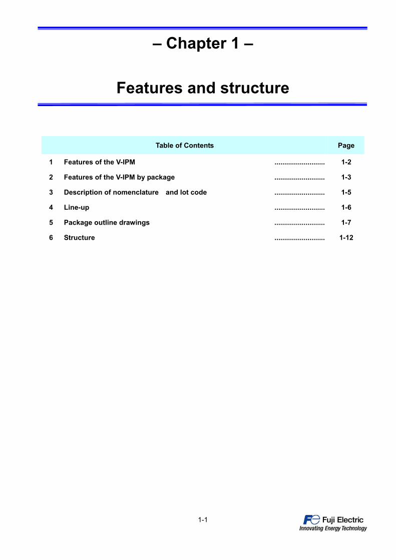
– Chapter 1 –
Features and structure
1-1
Table of Contents Page
1 Features of the V-IPM .......................... 1-2
2 Features of the V-IPM by package .......................... 1-3
3 Description of nomenclature and lot code .......................... 1-5
4 Line-up .......................... 1-6
5 Package outline drawings .......................... 1-7
6 Structure .......................... 1-12

Chapter 1 Features and structure
1-2
1 Features of the V-IPM
An IPM (intelligent power module) is an intelligent IGBT module combining a built-in control IC which
includes a drive circuit and a protection circuit. The V-IPM (V-series IPM) has the following features:
1.1 VR-IGBT chip
・Trade-off characteristic between the turn-off switching energy (Eoff) and the saturation voltage (Vce(sat)) is
improved by applying the 6th generation IGBT (V-series), so that the total loss is reduced.
1.2 Built-in drive circuit
• Drives the IGBT under the optimized gate control conditions.
• No negative power supply is needed since it has minimum gate impedance between the drive circuit
and the IGBT devices.
• Four isolated power supply units are required: one (1) on the lower arm side, three (3) on the upper
arm side.
1.3 Built-in protection circuit
• Overcurrent protection (OC), short-circuit protection (SC), controlled power supply under voltage
protection (UV), overheat protection (TjOH) and an external alarm output (ALM) are integrated.
• OC and SC are functions to protect the IGBT against breakdown caused by an over current or a load
short-circuit. Each IGBT has an on-chip current sensor which can detect the collector current of each
IGBT. This feature can protect the IPM module against an over current and a short circuit that may
occur in any IGBT.
• UV is the protective function that works against a drive power supply voltage drop. Every control IC
has this function.
• TjOH provides a high-speed over temperature protection by using an on-chip temperature sensor.
• ALM sends an alarm signal to the outer peripheral control unit of the IPM when an OC, SC, UV
and/or TjOH occur. Additionally the IPM initiates a safe soft stop of the system. *1
*1 See [Chapter 3 Description of functions] for details of protective functions of each IPM.
1.4 Built-in brake circuit (7in1 IPM)
• A brake circuit can be configured by adding an external resistor that consumes electric power during
regeneration.
• The brake circuit has a drive circuit and protection circuit, same as the inverter unit.
1.5 RoHS compliant
• All products of the V-IPM series are compliant with the RoHS directive.

Chapter 1 Features and structure
1-3
2 Features of the V-IPM by package
2.1 Low power type (P629: 6in1 with lower arm alarm output)
20 A to 50 A for 600V and 10 A to 25 A for 1200V are lined up as the low power type V-IPM.
(P629 package)
• P629 package has a copper base plate with excellent heat dissipation performance.
• Terminal pitch of the control terminals is a standard 2.54 mm (0.1 inch).
• Main terminals are flat type solder pin and the height is the same as the control terminals.
Therefore, it enables to solder the main terminals and control terminals to the same PCB.
• The IGBT is protected against abnormal overheating by an on-chip temperature sensor. *1
• Over current protection is realized by the on-chip sense IGBT current sensor. *1
• Compatible mounting dimensions with the R-IPM-series P619 package.
*1 Although the protective function is applied to the upper arm side, but no alarm output function is
available for the upper arm.
2.2 Medium-power small-package type (P626: 6in1 with upper and lower arm alarm output)
50A to 75A for 600V and 25A to 50A for 1200V are lined up as the medium-power small-size package
type.
(P626 package)
• Terminal pitch of the control input terminals is a 2.54mm (0.1inch) standard pitch.
• Main terminals are flat type solder pin and the height is the same as the control terminals.
Therefore it enables the main and control terminals to be soldered to the same PCB
• The IGBT is protected against abnormal overheating by an on-chip temperature sensor
• Over current protection is realized by the on-chip sense IGBT current sensor.
2.3 Medium-power thinner package type (P630: 6in1 / 7in1 with upper and lower arm alarm
output function)
50A to 200A for 600V and 25A to 100A for 1200V are lined up as the medium-power thinner package type.
Additionally, there is a low thermal impedance type for 100A ~ 200A/600V and 50A ~ 100A/1200V.
(P630 package)
• Terminal pitch of the control input terminals is a 2.54mm (0.1inch) standard pitch that can be
connected by using a general-purpose connector or by soldering.
Guide pins assist insertion of a PCB to the IPM.
• Screw size for the main terminals is M4.

Chapter 1 Features and structure
1-4
• The screw size for mounting to the heat sink is M4, which is the same as the main terminals.
• Solder less connection is also possible for electrical connection (main terminals and control terminals),
which facilitates easy disconnection.
• The IGBT is protected against abnormal overheating by an on-chip by the on-chip temperature sensor.
• Over current protection is realized by the on-chip sense IGBT.
2.4 High power type (6in1 / 7in1 with upper and lower arm alarm output function)
200A to 400A for 600V and 100A to 200A for 1200V are lined up as the high power type
(P631 package)
• Main DC bus input terminals (P1, P2, N1, N2), brake terminal (B) and output terminals (U, V, W) are
located in proximity to each other and the package structure permits easy main wiring. Terminals P1,
P2 and terminals N1, N2 are electrically connected to each other respectively.
• Screw size for the main terminals is M5 which allows large current.
• The screw size for mounting to a heat sink is M5, which is the same size as the main terminals.
• Solder less electrical connection is also possible and it can realize easy disconnection.
• The IGBT is protected against abnormal overheating by an on-chip temperature sensor.
• This package has two different boss heights. The PCB height from the base of the IPM can be set to
17.0 mm or 18.5 mm by changing the boss height (See Figure 1-12).
• Over current protection is realized by the on-chip sense IGBT.
• Mounting dimensions are compatible with the R-IPM-series P612 package products (excluding control
terminal positions).
2.5 Medium power small package type (6in1 / 7in1 with upper and lower arm alarm output)
50A to 100A for 600V and 25A to 50A for 1200V are lined up as the medium power type (P636 package)
• Terminal pitch of the control input terminals is a 2.54mm (0.1inch) standard pitch.
• Main terminals are flat type solder pin and the height is the same as the control terminals.
It enables the main and control terminals to be soldered to the same PCB
• The IGBT is protected against abnormal overheating by an on-chip temperature sensor.
• Over current protection is realized by the on-chip sense IGBT current sensor.

Chapter 1 Features and structure
1-5
3 Description nomenclature and lot code
• Type
• Lot number
2 1 0 0 0
1: January
O: OctoberN: NovemberD: December
2: 20123: 20134: 2014
Sequential number (001 to 999)
Year of production
Month of production
・・・
・・・
• Label
50A 600V
Lot No.
Data matrix
6MBP50VBA060-50
Country of productionand place of production
6 MBP 50 V B A 060 -50
060: 600 V120: 1200 V
A: P629 B: P626 D: P630 E: P631
Current rating
Model sequential number (< 50: Non-RoHS, >=50: RoHS)
Voltage rating
Package
Series name
Series sequential number
F: P636
Number of the main IGBT elements
6: 6 IGBTs without brake7: 6 IGBTs with built-in brake
Represents “IGBT-IPM”
Chapter 1 Features and structure
1-6
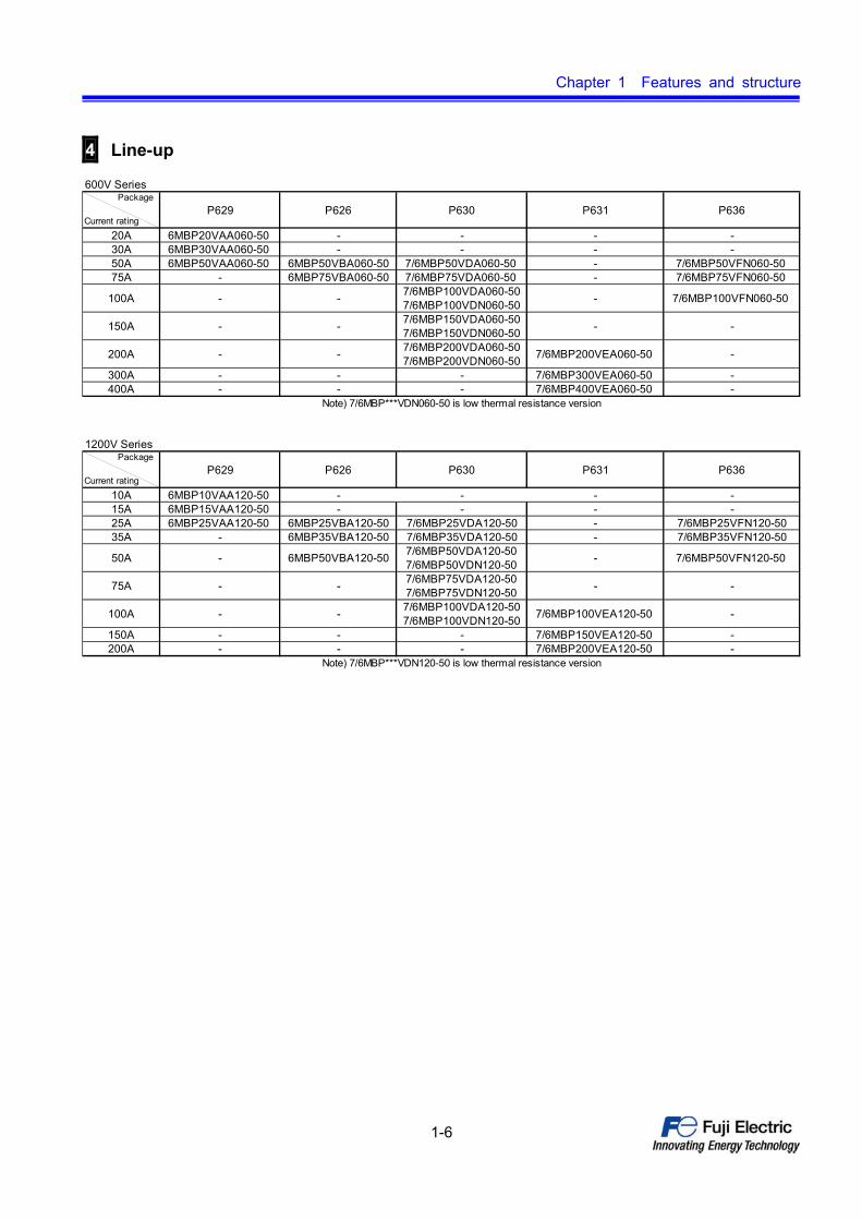
4 Line-up
600V Series Package
Current ratingP629 P626 P630 P631 P636
20A 6MBP20VAA060-50 - - - -30A 6MBP30VAA060-50 - - - -50A 6MBP50VAA060-50 6MBP50VBA060-50 7/6MBP50VDA060-50 - 7/6MBP50VFN060-50 75A - 6MBP75VBA060-50 7/6MBP75VDA060-50 - 7/6MBP75VFN060-50
100A - -7/6MBP100VDA060-507/6MBP100VDN060-50
- 7/6MBP100VFN060-50
150A - -7/6MBP150VDA060-507/6MBP150VDN060-50
- -
200A - -7/6MBP200VDA060-507/6MBP200VDN060-50
7/6MBP200VEA060-50 -
300A - - - 7/6MBP300VEA060-50 -400A - - - 7/6MBP400VEA060-50 -
Note) 7/6MBP***VDN060-50 is low thermal resistance version
1200V Series Package
Current ratingP629 P626 P630 P631 P636
10A 6MBP10VAA120-50 - - - -15A 6MBP15VAA120-50 - - - -25A 6MBP25VAA120-50 6MBP25VBA120-50 7/6MBP25VDA120-50 - 7/6MBP25VFN120-5035A - 6MBP35VBA120-50 7/6MBP35VDA120-50 - 7/6MBP35VFN120-50
50A - 6MBP50VBA120-507/6MBP50VDA120-507/6MBP50VDN120-50
- 7/6MBP50VFN120-50
75A - -7/6MBP75VDA120-507/6MBP75VDN120-50
- -
100A - -7/6MBP100VDA120-507/6MBP100VDN120-50
7/6MBP100VEA120-50 -
150A - - - 7/6MBP150VEA120-50 -200A - - - 7/6MBP200VEA120-50 -
Note) 7/6MBP***VDN120-50 is low thermal resistance version

Chapter 1 Features and structure
1-7
5 Package outlines
Figure 1-1 Package outline drawing for P629
Target type: 6MBP20VAA060-50, 6MBP30VAA060-50, 6MBP50VAA060-50,
6MBP10VAA120-50, 6MBP15VAA120-50, 6MBP25VAA120-50
注) 1.は理論寸法を示す。
2.端子ピッチは根元寸法とする。
3.( )内寸法は、参考値とする。
4.端子: Sn-Cuメッキ
(半田付け仕様)
[寸法:mm]
Note: 1. The dimensions shown in fig. 1-1 represent the theoretical dimension.
2. The terminal pitch is the value at the root of the terminal.
3. Dimensions in brackets are given only for reference.
4. Terminal plating: Sn (for soldering) [Unit of dimensions: mm]

Chapter 1 Features and structure
1-8
Figure 1-2 Package outline drawing for P626
Target type: 6MBP50VBA060-50, 6MBP75VBA060-50,
6MBP25VBA120-50, 6MBP35VBA120-50, 6MBP50VBA120-50
注) 1.は理論寸法を示す。
2.端子ピッチは根元寸法とする。
3.端子: Sn-Cuメッキ
(半田付け仕様)
[寸法:mm]
Note: 1. The dimensions shown in fig. 1-2 represent the theoretical dimension.
2. The terminal pitch is the value at the root of the terminal.
3. Terminal plating: Sn (for soldering use)
[Unit of dimensions: mm]

Chapter 1 Features and structure
1-9
Figure 1-3 Package outline drawing for P630
Target type:
7/6MBP50VDA060-50, 7/6MBP75VDA060-50, 7/6MBP100VDA060-50, 7/6MBP100VDN060-50, 7/6MBP150VDA060-50,
7/6MBP150VDN060-50, 7/6MBP200VDA060-50, 7/6MBP200VDN060-50, 7/6MBP25VDA120-50, 7/6MBP35VDA120-50,
7/6MBP50VDA120-50, 7/6MBP50VDN120-50, 7/6MBP75VDA120-50, 7/6MBP75VDN120-50, 7/6MBP100VDA120-50,
7/6MBP100VDN120-50
Note: 1. The dimensions shown in fig. 1-3 represent the theoretical dimension. 2. The terminal pitch is the value at the root of the terminal. 3. Dimensions given in brackets are for reference. 4. Main terminal plating: Ni
Control terminal plating: Ni plating on the ground, Au plating on the surface.(for connector and soldering use)
5. The guide pins located on both sides of a control terminal are made of brass. (They are insulated internally and are not connected to any object.)
[Unit of dimensions: mm]

Chapter 1 Features and structure
1-10
Figure 1-4 Package outline drawing for P631
Target type: 7/6MBP200VEA060-50, 7/6MBP300VEA060-50, 7/6MBP400VEA060-50,
7/6MBP100VEA120-50, 7/6MBP150VEA120-50, 7/6MBP200VEA120-50
注) 1.は理論寸法を示す。
2.端子ピッチは根元寸法とする。
3.( )内寸法は、参考値とする。
4.主端子: Niメッキ
制御端子: 下地Ni+表面Auメッキ
(コネクタ、半田付け仕様)
5.制御端子両側にあるガイドピンは、黄銅(しんちゅう)です。
(内部は、絶縁されており、どの部分にも接続されていません。)
[寸法:mm]
Note: 1. The dimensions shown in fig. 1-4represent the theoretical dimension. 2. The terminal pitch is the dimension measured at the root. 3. Dimensions given in brackets are for reference only. 4. Main terminal plating: Ni
Control terminal plating: Ni plating on the ground, Au plating on the surface.(for connector rand soldering use)
5. The guide pins located on both sides of a control terminal are made of brass. (They are insulated internally and are not connected to any object.)
[Unit of dimensions: mm]

Chapter 1 Features and structure
1-11
Figure 1-5 Package outline drawing for P636
Target type: 7/6MBP50VFN060-50, 7/6MBP75VFN060-50, 7/6MBP100VFN060-50,
7/6MBP25VFN120-50, 7/6MBP35VFN120-50, 7/6MBP50VFN120-50
Note: 1. The dimensions shown in fig. 1-5 represent the theoretical dimension.
2. The terminal pitch is the value at the root of the terminal.
3. Terminal plating: Sn (for soldering use) [Unit of dimensions: mm]

Chapter 1 Features and structure
1-12
6 Structure
* This drawing is prepared for explanation of the material. It does not represent accurate chip size or layout.
No. Component Material (main) Remarks
1 Isolation substrate Ceramic
2 IGBT chip Silicon
3 FWD chip Silicon
4 Printed Circuit Board (PCB) Glass reinforced Epoxy resin Halogen Free
5 IC chip Silicon
6 Base Plate Cu Ni plating
7 Main Terminal Cu Sn plating
8 Lid PPS resin UL 94V-0
9 Case PPS resin UL 94V-0
10 Wiring Aluminum
11 Silicone Gel Silicone resin
12 Control Terminal Brass Sn plating
Figure 1-6 Structure and material list (P629)

Chapter 1 Features and structure
1-13
* This drawing is prepared for explanation of the material. It does not represent accurate chip size or layout.
No. Component Material (main) Remarks
1 Isolation substrate Ceramic
2 IGBT chip Silicon
3 FWD chip Silicon
4 Printed Circuit Board (PCB) Glass reinforced Epoxy resin Halogen Free
5 IC chip Silicon
6 Base Plate Cu Ni plating
7 Main Terminal Cu Sn plating
8 Lid PPS resin UL 94V-0
9 Case PPS resin UL 94V-0
10 Wiring Aluminum
11 Silicone Gel Silicone resin
12 Ring SUS
13 Control Terminal Brass Sn plating
Figure 1-7 Structure and material list (P626)

Chapter 1 Features and structure
1-14
* This drawing is prepared for explanation of the material. It does not represent accurate chip size or layout.
No. Component Material (main) Remarks
1 Isolation substrate Ceramic
2 IGBT chip Silicon
3 FWD chip Silicon
4 Printed Circuit Board (PCB) Glass reinforced Epoxy resin Halogen Free
5 IC chip Silicon
6 Base Plate Cu Nickel plating
7 Main Terminal Cu Surface: Ni plating
8 Lid PPS resin UL 94V-0
9 Case PPS resin UL 94V-0
10 Wiring Aluminum
11 Silicone Gel Silicone resin
12 Ring SUS
13 Nut Fe Trivalent chromate treatment
14 Control terminal Brass Au plating on Ni plating
15 Guide pin Brass
Figure 1-8 Structure and material list (P630)

Chapter 1 Features and structure
1-15
* This drawing is prepared for explanation of the material. It does not represent accurate chip size or layout.
No. Component Material (main) Remarks
1 Isolation substrate Ceramic
2 IGBT chip Silicon
3 FWD chip Silicon
4 Printed Circuit Board (PCB) Glass reinforced Epoxy resin Halogen Free
5 IC chip Silicon
6 Base Plate Cu Nickel plating
7 Main Terminal Cu Surface: Ni plating
8 Lid PPS resin UL 94V-0
9 Case PPS resin UL 94V-0
10 Wiring Aluminum
11 Silicone Gel Silicone resin
12 Ring SUS
13 Nut Fe Trivalent chromate treatment
14 Control terminal Brass Au plating on Ni plating
15 Guide pin Brass
Figure 1-9 Structure and material list (P631)

Chapter 1 Features and structure
1-16
* This drawing is prepared for explanation of the material. It does not represent accurate chip size or layout.
No. Component Material (main) Remarks
1 Isolation substrate Ceramic
2 IGBT chip Silicon
3 FWD chip Silicon
4 Printed Circuit Board (PCB) Glass reinforced Epoxy resin Halogen Free
5 IC chip Silicon
6 Base Plate Cu Ni plating
7 Main Terminal Cu Sn plating
8 Lid PPS resin UL 94V-0
9 Case PPS resin UL 94V-0
10 Wiring Aluminum
11 Silicone Gel Silicone resin
12 Ring SUS
13 Control Terminal Brass Sn plating
Figure 1-10 Structure and material list (P636)
Chapter 1 Features and structure
1-17
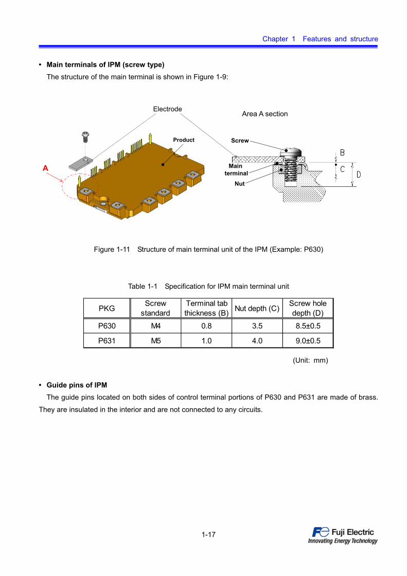
• Main terminals of IPM (screw type)
The structure of the main terminal is shown in Figure 1-9:
Area A section
Figure 1-11 Structure of main terminal unit of the IPM (Example: P630)
Table 1-1 Specification for IPM main terminal unit
PKGScrew
standardTerminal tabthickness (B)
Nut depth (C)Screw holedepth (D)
P630 M4 0.8 3.5 8.5±0.5
P631 M5 1.0 4.0 9.0±0.5
(Unit: mm)
• Guide pins of IPM
The guide pins located on both sides of control terminal portions of P630 and P631 are made of brass.
They are insulated in the interior and are not connected to any circuits.
A
Product
Main terminal
Nut
Screw
Electrode

Chapter 1 Features and structure
1-18
• Height of boss on lid of P636
P636 package has two different boss heights (2.5 mm and 1.0 mm) on the lid. The PCB height can be set
to 18.5 mm or 17.0 mm by changing the boss height.
Figure 1-12 Selecting from two different boss heights
2.5mm
18.5mm
PCB
1.0mm
17.0mm
PCB
2.5mm boss
1.0mm bossInsert 2.5mm bossthrough a hole in the PCB

– Chapter 2 –
Description of terminal marking and terms
2-1
Table of Contents Page
1 Description of terminal marking ............................................ 2-2
2 Description of terms ............................................ 2-3

Chapter 2 Description of terminal marking and terms
2-2
1 Descriptions of the I/O terminals
Main terminals
TerminalName
BUVW
P (P1, P2)N (N1, N2)
DC-bus terminals after smoothing capacitorP: + side, N: - side
3-phase output terminals
Description
Collector terminal of the Brake IGBT. Connect a brake resistor for dissipating regenerated energy
* P1, P2, N1 and N2 terminals are P631 package only.
Control terminals
TerminalName
P629Pin#
P626, P630,P636Pin#
P631Pin# Description
GND U 1 1 1 Ground reference for the U-arm control power supplyVcc U 3 4 3 U-arm control power supply positive terminalVin U 2 3 2 U-arm control signal inputALM U - 2 4 U-arm alarm signal outputGND V 4 5 5 Ground reference for the V-phase control power supplyVcc V 6 8 7 V-arm control power supply positive terminalVin V 5 7 6 V-arm control signal input
ALM V - 6 8 V-arm alarm signal outputGND W 7 9 9 Ground reference for the W-phase control power supplyVcc W 9 12 11 W-arm control power supply positive terminalVin W 8 11 10 W-arm control signal inputALM W - 10 12 W-arm alarm signal outputGND 10 13 13 Ground reference for the lower arm control power supplyVcc 11 14 14 Control power supply positive terminal for the lower arm
Vin X 12 16 16 X-arm control signal inputVin Y 13 17 17 Y-arm control signal inputVin Z 14 18 18 Z-arm control signal input
Vin DB - 15 15 DB-arm control signal inputALM 15 19 19 Lower-arm alarm signal output
* Pin (15) of P626 is of no contact.
* Pin (15) of each of P631 (6in1), P630 (6in1) is of no contact.

Chapter 2 Description of terminal marking and terms
2-3
2 Description of terms
2.1 Absolute maximum rating
Symbol DescriptionVDC Maximum DC bus voltage between the P and N terminal
VSCMaximum DC bus voltage between the P and N terminal during short-circuitprotection and over current protection
VCESMaximum voltage between the collector and emitter terminal of the built-inIGBT, and peak inverse voltage of the FWD.
IC Maximum DC collector current for each IGBTICP Maximum peak collector current for each IGBT-IC Maximum DC forward current for each FWDIF Maximum DC forward current for FWD in brake circuitPC Maximum power dissipation for each IGBT at Tc=25oC, Tj≤150oCVCC Maximum voltage between the VCC and GND terminalVin Maximum voltage between the Vin and GND terminal
VALM Maximum voltage between the ALM and GND terminalTj Maximum IGBT/FWD chip junction temperature during continuous operation
ToprAllowable case temperature range during operation (measured point of thecase temperature Tc is shown in Figure 5-4)
TstgAllowable ambient temperature during storage or transportation withoutbeing subject to electrical load.
Tsol Maximum temperature for soldering the terminals to a PCB
VisoMaximum RMS isolation of sinusoidal voltage between all the terminals andheat sink (all terminals are shorted)
Terminal - Maximum screw torque for the main terminal with specified screw
Mounting - Maximum screw torque for mounting the IPM on heat sink with specifiedscrew
Diode forward current for DBCollector lossControl power supply voltageInput voltageAlarm voltageChip junction temperature
Case temperature during operation
Storage temperature
Soldering temperature
Isolation voltage
Screw torque
TermDC power supply voltage
DC power supply voltage at short circuit
Collector-Emitter blocking voltage
Collector current
2.2 Electrical characteristics
2.2.1 Main circuit Symbol Description
ICESLeakage current when specified voltage is applied between the collector andemitter and all input signals are "H" (=all IGBTs are turned-off).
VCE(sat)Voltage drop between the collector and emitter when gate input signal is "L"(=IGBT is turned-on)
VFVoltage drop across the diode at defined forward current at input signal is"H" (=IGBT is turned of)
ton
Time interval between the moment when gate input voltage has exceedVinth(on) and the collector current has increased to 90% of the loadcurrent. (see Figure 2-1)
toff
Time interval between the moment when the gate input voltage hasdropped less than Vinth(off) and the corrector current drops to 10% of theload current. If the collector dropping waveform is not a straight line, atangential line is used as the substitute (see Figure 2-1)
tfTime interval the collector current decreased from 90% to 10% of the loadcurrent
trrTime interval between the moment when the collector current exceeds100% of the load current and the reverse recovery current disappears
tdead Time delay of the turn-on signal from the alternate IGBT turn-off signal.
Fall time
Reverse recovery time
Dead time
Collector-Emitter leakage current
Collector-Emitter saturation voltage
Diode forward voltage
Turn-on time
Turn-off time
Term
Chapter 2 Description of terminal marking and terms
2-4
2.2.2 Control circuit
Term Symbol DescriptionICCP Current flows into VCC terminal of upper arm control power supplyICCN Current flows into VCC terminal of lower arm control power supply
Vinth(on)Voltage above which considerable the control IC can detect theinput signal as ON
Vinth(off)Voltage below which considerable the control IC can detect theinput signal as OFF
Control power supply consumptioncurrent
Input threshold voltage
2.2.3 Protection circuit
Term Symbol Description
Over current protection current ICCPCurrent flows into the VCC terminal of upper arm control powersupply
Over current interruption lag time tdocLag time since the over current reaches the trip level until theprotection start. See Figure 2-3
Short-circuit protection current ISC Threshold current for short-circuit protection
Short-circuit protection lag time tSCLag time since the short circuit current reaches the trip level untilthe protection start. See Figure 2-4
Chip over heat protection temperature TjOH Threshold junction temperature for overheat protection
Chip over heat protection hysteresis TjHLower hysteresis offset temperature to reactivate after the overtemperature protection
Control power supply under voltageprotection voltage
VUV Trip voltage to start under-voltage protection
Control power supply under voltageprotection hysteresis
VHHigher threshold offset voltage to reactivate after the low voltageprotection
tALM(OC) Alarm signal pulse width of the overcurrent protection (OC)tALM(UV) Alarm signal pulse width of under the voltage protection (UV)
tALM(TjOH) Alarm signal pulse width of the overheat protection (TjOH)
Alarm output resistance RALMValue of the built-in resistance that is connected in series to alarmterminals. It limits the primary forward current of opto-coupler.
Alarm output hold time
2.3 Thermal characteristics
Term Symbol DescriptionRth(j-c)Q Thermal resistance between the case and IGBT chipRth(j-c)D Thermal resistance between the case and FWD chip
Thermal resistance between case andheat sink
Rth(c-f)Thermal resistance between the case and heat sink at thecondition
Case temperature TCIPM case temperature (bottom surface of the cupper base platedirectly under the chip)
Thermal resistance between chip andcase
2.4 Noise tolerance
Term Symbol DescriptionCommon mode - Common mode noise tolerance in our test circuit

Chapter 2 Description of terminal marking and terms
2-5
2.5 Others
Term Symbol DescriptionMass Wt Mass of the IPM
Switching frequency fSWAllowable switching frequency for the control signals to the inputterminals.
Reverse recovery current Irr Peak value of the reverse recovery current. See Figure 2-1.
Reverse bias safe operating area RBSOA
The area of the voltage and current which the device can operatewithout self-damage during turn-off switching.There is a possibility to brake down when voltage or currentexceed the area.
Eon Dissipated switching energy of the IGBT during turn-onEoff Dissipated switching energy of the IGBT during turn-offEorr Dissipated switching energy of the FWD during reverse recovery
Inverse voltage VR Repetitive reverse peak voltage of the FRD chip in the brake unitInput current Iin Maximum current into the Vin terminals
Switching loss

Chapter 2 Description of terminal marking and terms
2-6
Figure 2-1 Switching times
Figure 2-2 Input/output timing diagram
toff
trrInput signal
Collector current
tf
on
90%
ton
90%
10%
Vinth(on) Vinth(off) off
Irr
ON
With protection factor
Protected period
tALM
OFF
Protection factor
VALM
Vin
IC
IGBTguardstate
High
Low
High
Low
Withoutprotection factor

Chapter 2 Description of terminal marking and terms
2-7
Figure 2-3 Overcurrent interruption lag time (tdoc)
IC
VALM
tSC
Isc
Figure 2-4 Short-circuit protection lag time (tsc)
alarmAlarm output
Input signal on
≧tdoc① ②
< tdoc
Collector current
off
IOC
Chapter 2 Description of terminal marking and terms
2-8
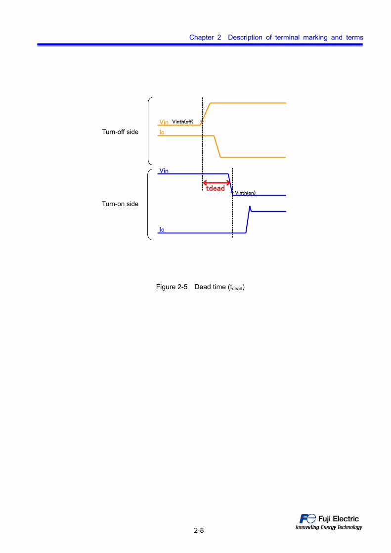
Figure 2-5 Dead time (tdead)
Vin
tdead
ターンオフ側
Vinth(off)
Vinth(on)
Ic
Vin
Ic
ターンオン側
Turn-off side
Turn-on side
– Chapter 3 –
Description of functions
3-1
Table of Contents Page
1 List of functions ............................................ 3-2
2 Description of functions ............................................ 3-4
3 Truth table ............................................ 3-10
4 Block diagram ............................................ 3-12
5 Timing chart ............................................ 3-20

Chapter 3 Description of functions
3-2
1 List of functions
The built-in protection functions in the V-IPM are shown in Tables 3-1 and 3-2.
Table 3-1 IPM built-in functions, 600 V-series
Upperarm
Lowerarm
Drive UV TjOH ALM ALM
- - -
P630
Numberof
Switch
6MBP50VBA060-50
6MBP75VBA060-50
6MBP20VAA060-50
6MBP30VAA060-50
6MBP50VAA060-50
6 in 1
6MBP75VDA060-50
6MBP150VDA060-50
6MBP400VEA060-50
6MBP50VFN060-50
6MBP75VFN060-50
6MBP100VFN060-50
Built-in Function
PackageType Name
6MBP50VDA060-50
P629
P626
Upper and Lower arms
OC / SC
P630
6MBP100VDA060-50
6MBP200VDA060-50
6MBP200VEA060-50
6MBP300VEA060-50
6MBP100VDN060-50
6MBP150VDN060-50
6MBP200VDN060-50
P636
P631
7 in 1
7MBP50VFN060-50
7MBP100VDN060-50
7MBP150VDN060-50
7MBP400VEA060-50
7MBP50VDA060-50
7MBP75VDA060-50
7MBP100VDA060-50
7MBP150VDA060-50
7MBP200VDA060-50
7MBP200VEA060-50
P636
7MBP200VDN060-50
7MBP75VFN060-50 7MBP100VFN060-50
P6317MBP300VEA060-50
Drive: IGBT drive circuit, UV: Control power supply under voltage protection, TjOH: Chip temperature
overheat protection, OC: Overcurrent protection, SC: Short-circuit protection, ALM: Alarm signal output

Chapter 3 Description of functions
3-3
Table 3-2 IPM built-in functions, 1200 V-series
Upperarm
Lowerarm
Drive UV TjOH ALM ALM
- - -
7MBP35VFN120-507MBP50VFN120-50
7 in 1
P636
P636
7MBP75VDN120-50
7MBP100VDN120-50
P630
6 in 1
6MBP25VFN120-50
6MBP35VFN120-50
6MBP50VFN120-50
7MBP25VFN120-50
6MBP50VDN120-50
6MBP75VDN120-50
6MBP100VDN120-50
7MBP50VDN120-50
OC / SC
7MBP100VDA120-50
7MBP75VDA120-50
Numberof
SwitchType Name
7MBP50VDA120-50
7MBP25VDA120-50
7MBP35VDA120-50
6MBP200VEA120-50
6MBP75VDA120-50
6MBP100VDA120-50
6MBP100VEA120-50
6MBP150VEA120-50
Package
7MBP100VEA120-50
7MBP150VEA120-50
7MBP200VEA120-50
6MBP10VAA120-50
6MBP15VAA120-50
6MBP25VAA120-50
Upper and Lower arms
P631
6MBP25VBA120-50
6MBP35VBA120-50
6MBP50VBA120-50
6MBP25VDA120-50
6MBP35VDA120-50
6MBP50VDA120-50
Built-in Function
P626
P631
P629
P630
Drive: IGBT drive circuit, UV: Control power supply under voltage protection, TjOH: Chip temperature
overheat protection, OC: Overcurrent protection, SC: Short-circuit protection, ALM: Alarm signal output

Chapter 3 Description of functions
3-4
N-sidePWM input
P-sidePWM input
Brakeinput
P
B
N
UVW
IPM
Pre-Driver Pre-Driver Pre-Driver
Alarmoutput
Alarmoutput
Alarmoutput
Pre-Driver Pre-Driver Pre-Driver
Alarmoutput
Pre-Driver
2 Description of functions
2.1 IGBT and FWD for 3-phase inverter
The V-IPM has a 3-phase bridge circuit which consists of six IGBTs and six FWDs as shown in Figure 3-1.
The main circuit is completed when the main DC bus power supply line is connected to the P and N
terminals and the 3-phase output line is connected to the terminals U, V and W. Connect a snubber circuit
to suppress the surge voltage.
2.2 IGBT and FWD for brake
IGBT and FWD for brake circuit are integrated in the V-IPM (7in1 of P630 and P631 series). The collector
terminal of the IGBT is connected to the output terminal B as shown in Figure 3-1. The regenerative energy
during deceleration is consumed by the resistor which is connected between terminal P and B. Voltage rise
between terminals P and N can be suppressed by switching the brake IGBT.
Figure 3-1 Typical application of 3-phase inverter (Example: 7MBP200VDA060-50 with built-in brake)

Chapter 3 Description of functions
3-5
2.3 IGBT drive function
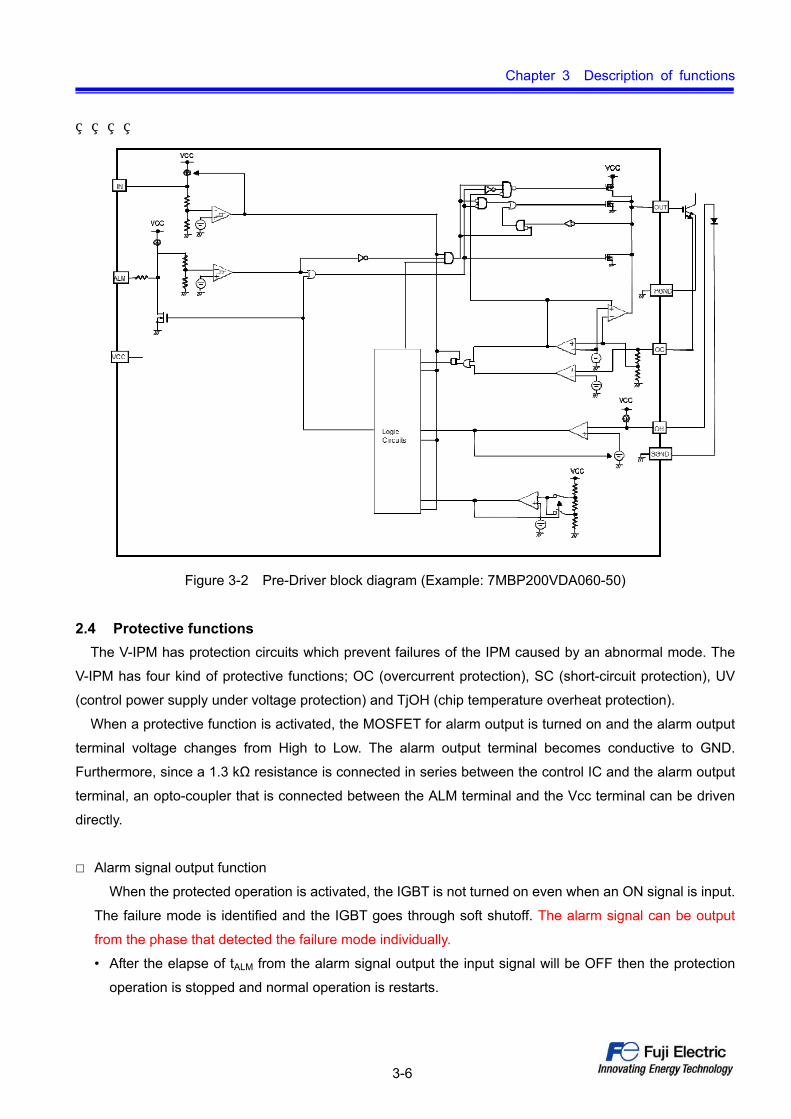
Figure 3-2 shows a block diagram of the Pre-Driver. The V-IPM has a built-in gate drive circuit for the
IGBT and it is possible to drive the IGBT by inputting an opto-isolated control signal to the V-IPM without
designing the gate resistance value.
The features of this drive function are introduced below:
Independent turn-on and turn-off control
The V-IPM has an independent gate drive circuits for turn-on and turn-off of the IGBT instead of a
single gate resistance. The drive circuits control the dv/dt of turn-on and turn-off independently and
maximize the performance of the device.
Soft shutoff
The gate voltage is gradually reduced at the occasion of the IGBT shutoff when the protection function
is activated in various kinds of abnormal modes. The soft shutoff suppresses the surge voltage during
the turn-off and prevents the breakdown of the device.
Prevention of false turn-on
The gate electrode of the IGBT is connected to the grounded emitter with low impedance. It prevents
false turn-on of the IGBT due to the increase of the VGE due to noise or other cause.
No reverse bias power supply is necessary
The wiring length between the control IC and the IGBT in the V-IPM are short and the wiring
impedance is small, therefore the V-IPM can be driven without reverse bias.
Chapter 3 Description of functions
3-6
Figure 3-2 Pre-Driver block diagram (Example: 7MBP200VDA060-50)
2.4 Protective functions
The V-IPM has protection circuits which prevent failures of the IPM caused by an abnormal mode. The
V-IPM has four kind of protective functions; OC (overcurrent protection), SC (short-circuit protection), UV
(control power supply under voltage protection) and TjOH (chip temperature overheat protection).
When a protective function is activated, the MOSFET for alarm output is turned on and the alarm output
terminal voltage changes from High to Low. The alarm output terminal becomes conductive to GND.
Furthermore, since a 1.3 kΩ resistance is connected in series between the control IC and the alarm output
terminal, an opto-coupler that is connected between the ALM terminal and the Vcc terminal can be driven
directly.
Alarm signal output function
When the protected operation is activated, the IGBT is not turned on even when an ON signal is input.
The failure mode is identified and the IGBT goes through soft shutoff. The alarm signal can be output
from the phase that detected the failure mode individually.
• After the elapse of tALM from the alarm signal output the input signal will be OFF then the protection
operation is stopped and normal operation is restarts.

Chapter 3 Description of functions
3-7
• Even in case the alarm factor is dissolved within the alarm signal output period (tALM), the protected
operation continues during the alarm signal output period (tALM), and accordingly, the IGBT is not
turned on.
Furthermore, the alarm circuits for the lower arm devices including brake circuit are connected
mutually. If protection operation occurs on the lower arm side, all the IGBTs of the lower arms are turned
off during the protection operation.
* P629 package has protective functions on both of the upper arm and the lower arm devices, but the
upper arm devices do not have an alarm signal output function. The lower arm devices have both, the
protective functions and alarm signal output function.
Alarm factor identification function
As the alarm signal output period (tALM) varies in correspondence to the failure mode, the failure mode
can be identified by measuring the alarm signal pulse width.
Alarm factor Alarm signal output period (tALM)
Overcurrent protection (OC)
Short-circuit protection (SC) 2 ms (typ.)
Control power supply under
voltage protection (UV) 4 ms (typ.)
Chip temperature overheat
protection (TjOH) 8 ms (typ.)
However, the pulse width of the alarm signal output through an optocoupler varies by the influence of a
time delay of the optocoupler and other peripheral circuits. It is necessary to take these influences into
account in your design.

Chapter 3 Description of functions
3-8
2.5 Overcurrent protection function: Over Current (OC)
The IGBT’s forward collector current is measured by the current sense IGBT built in the IGBT chip. When
the forward collector current exceeds the protection level (IOC) and continues longer than tdoc (typ. 5 µs), it
is judged as being in the OC status and the IGBT is turned off to prevent occurrence of breakdown by the
overcurrent. At the same time, an alarm signal is provided. The OC status alarm signal period (tALM) is 2 ms.
• Protection operation is stopped and normal operation is restarted if the current level is lower than the IOC
level and the input signal is OFF after 2 ms (tALM) of the alarm signal output.
• Even in case the current level goes back to below the IOC within the 2 ms (tALM), the protection operation
continues until the end of the period of 2 ms (tALM) elapses and accordingly the IGBT is not turned on.
2.6 Short-circuit protective function: Short Circuit (SC)
The SC protective function prevents the IPM form being damaged by the peak current during load
short-circuit and arm short-circuit. When the IGBT’s forward collector current exceeds the protection level
(ISC) and continues longer than tdsc, it is judged as being in the SC status and the protective function is
activated then the IGBT is softly turned off to prevent occurrence of breakdown by short-circuit. At the same
time an alarm signal is output. The SC status alarm signal output period (tALM) is 2 ms.
• Protection operation is stopped and normal operation is resumed if the current level is lower than the ISC
level and the input signal is OFF after 2 ms (tALM) of the alarm signal output.
• Even in case that the short circuit disappears within 2 ms (tALM), the protective operation continues until
the period of 2 ms (tALM) elapses and accordingly the IGBT is not turned on.
2.7 Control power supply under voltage protection function (UV)
The UV protective function prevents malfunction of the control IC caused by a voltage drop of the control
power supply voltage (VCC) and thermal breakdown of the IGBT caused by increase of the VCE (sat) loss.
When VCC is continuously below the voltage protection trip level (VUV) for a period of 20 µs, it is judged as
being in the UV status and the IGBTs are softly turned off to prevent malfunction and breakdown caused by
the control power supply voltage drop. When it is judged as being in the UV status, the protective function is
activated and the alarm signal is generated. The alarm signal output period (tALM) of the UV protection is 4
ms.

Chapter 3 Description of functions
3-9
• As hysteresis VH is provided, protection operation is stopped and normal operation is resumed, if VCC is
higher than (VUV + VH) and the input signal is OFF. A 4 ms (tALM) alarm signal will be send to the output
• Even in case the supply voltage exceeds (VUV + VH) within 4 ms (tALM), the protective operation continues
until the period of 4 ms (tALM) elapses, and accordingly, the IGBT is not turned on.
Furthermore, an alarm signal for judgment of the UV status is provided at the time of startup and
shutdown of the control power supply.
2.8 Chip temperature overheat protective function: IGBT chip Over Heat protection (TjOH)
The TjOH protective function includes the direct IGBT chip temperature detected by a built-in on-chip
temperature sensor on each IGBT chip. If the IGBT chip temperature is continuously higher than protection
trip level (TjOH) for 1.0 ms, it is judged as being in the overheat status, the TjOH protective function is
activated then the IGBTs are softly turned off to prevent a failure of the IGBT. At the same time an alarm
signal output is generated. The UV status alarm signal output period (tALM) is 8 ms.
• There is a hysteresis offset TjH, the protective operation is stopped and normal operation is resumed, if Tj
is below (TjOH – TjH) and the input signal is OFF after 8 ms (tALM) of the alarm signal output.
• Even in case the alarm signal disappears within 8 ms (tALM), the protected operation continues until the
period of 8 ms (tALM) elapses, and accordingly, the IGBT is not turned on.
A case temperature overheat protective function (TCOH), which is built in the former IPM series, is not
built in the V-IPM series. The IGBT chip overheat status is protected by the TjOH protective function.

Chapter 3 Description of functions
3-10
3 Truth table
The truth tables of the V-IPM series when protective function is activated are shown in Tables 3-3 to 3-5.
Table 3-3 Truth table (P629)
Alarm signal output
ALM-Low side
High
High
High
High
High
High
High
High
High
High
High
High
Low
Low
Low
Low
*
TjOH
IGBT
W-phaseV-phase
*
*
*
Lower arm side
*
OC
OC
*
UV
SC OFF
OFF
Alarm factor
*
* *
U-phase
OFF
OFF
* *
UV *
OC
TjOH
*
*
*
OC
UV
*
TjOH *
*
*
*
TjOH
UV
*SC
*
OFF *
*
*
*
* OFF *
OFF *
* * OFF
* * OFF
* * OFF
*
OFF**
*
*OFF
*
*OFFSC
* OFF *
* OFF
*
SC * OFF *
Lower arm side
X, Y and Z-phase
W-phase
V-phase
U-phase
* Dependent on the input signal.
Table 3-4 Truth table (P626)
ALM-U ALM-V ALM-WALM-Low
sideLow High High High
Low High High High
Low High High High
Low High High High
High Low High High
High Low High High
High Low High High
High Low High High
High High Low High
High High Low High
High High Low High
High High Low High
High High High Low
High High High Low
High High High Low
High High High Low
* *
*OFF*
OFF *
* OFF
SC
***OFFSC
**OFF*
Lower arm side
X, Y and Z-phase
W-phase
V-phase
U-phase
* *
OC
OC
TjOH
* *
OFF *
UV
Alarm signal output
* *
V-phase
*
*
*
OFF
*
IGBT
W-phaseLower arm
side* *
*
Alarm factorU-phase
OFF
OFF
OFF
UV *
OC
TjOH
*
*
*
SC
*
*
*
OC
UV
TjOH
UV
*
SC *
TjOH *
*
* OFF *
OFF *
*
*
* * OFF
* * OFF
* * OFF
OFF
* Dependent on the input signal.

Chapter 3 Description of functions
3-11
Table 3-5 Truth table (P630, P631 and P636)
ALM-U ALM-V ALM-WALM-Low
sideLow High High High
Low High High High
Low High High High
Low High High High
High Low High High
High Low High High
High Low High High
High Low High High
High High Low High
High High Low High
High High Low High
High High Low High
High High High Low
High High High Low
High High High Low
High High High Low
* *
*OFF*
OFF *
* OFF
SC
***OFFSC
**OFF*
Lower arm sideX, Y and Z-
phase
W-phase
V-phase
U-phase
* *
OC
OC
TjOH
* *
OFF *
UV
Alarm signal output
* *
V-phase
*
*
*
OFF
*
IGBT
W-phaseLower arm
side* *
*
Alarm factorU-phase
OFF
OFF
OFF
UV *
OC
TjOH
*
*
*
SC
*
*
*
OC
UV
TjOH
UV
*
SC *
TjOH *
*
* OFF *
OFF *
*
*
* * OFF
* * OFF
* * OFF
OFF
* Dependent on the input signal.
Chapter 3 Description of functions
3-12
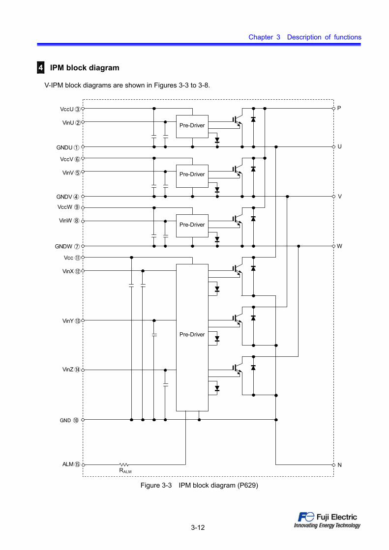
4 IPM block diagram
V-IPM block diagrams are shown in Figures 3-3 to 3-8.
Figure 3-3 IPM block diagram (P629)
U
V
W
Vcc ⑪
VinX ⑫
VinY ⑬
VinZ ⑭
ALM ⑮
VccV ⑥
GNDV ④
PVccU ③
GNDU ①
VinU ②
VinV ⑤
VccW ⑨
GNDW ⑦
VinW ⑧
GND ⑩
N
Pre-Driver
Pre-Driver
Pre-Driver
Pre-Driver
RALM

Chapter 3 Description of functions
3-13
Figure 3-4 IPM block diagram (P626)
Vcc ⑭
VinX ⑯
GND ⑬
VinY ⑰
VinZ⑱
ALM ⑲
VccV ⑧
GNDV⑤
VccU ④
GNDU①
VinU③
VinV ⑦
VccW ⑫
GNDW ⑨
VinW ⑪
⑮
ALMU ②
ALM V ⑥
ALM W ⑩
Pre-Driver
Pre-Driver
Pre-Driver
Pre-Driver
Pre-Driver
Pre-Driver
RALM
RALM
RALM
RALM
U
V
W
P
N
Chapter 3 Description of functions
3-14
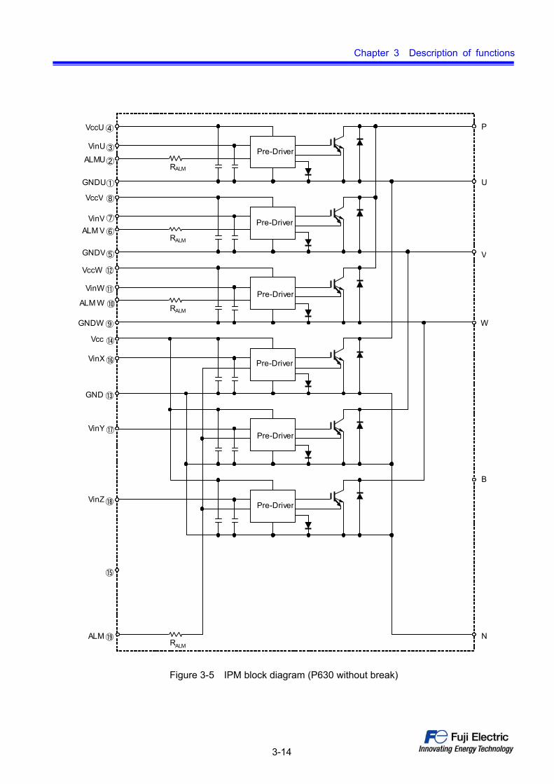
Figure 3-5 IPM block diagram (P630 without break)
Vcc ⑭
VinX ⑯
GND ⑬
VinY ⑰
VinZ⑱
ALM ⑲
VccV ⑧
GNDV⑤
VccU ④
GNDU①
VinU③
VinV ⑦
VccW ⑫
GNDW ⑨
VinW⑪
⑮
ALMU②
ALM V ⑥
ALM W ⑩
Pre-Driver
Pre-Driver
Pre-Driver
Pre-Driver
Pre-Driver
Pre-Driver
RALM
RALM
RALM
RALM
U
V
W
P
N
B

Chapter 3 Description of functions
3-15
Figure 3-6 IPM block diagram (P630 with built-in brake)
Pre-Driver
Pre-Driver
Pre-Driver
Pre-Driver
Pre-Driver
Pre-Driver
RALM
RALM
RALM
Pre-Driver
RALM
Vcc ⑭
VinX ⑯
GND ⑬
VinY ⑰
VinZ ⑱
ALM ⑲
B
VccV ⑧
GNDV ⑤
VccU ④
GNDU ①
VinU ③
VinV ⑦
VccW ⑫
GNDW ⑨
VinW ⑪
VinDB ⑮
ALMU ②
ALM V ⑥
ALM W ⑩
U
V
W
P
N

Chapter 3 Description of functions
3-16
Figure 3-7 IPM block diagram (P631 without brake)
VCC ⑭
VinX ⑯
GND ⑬
VinY ⑰
VinZ ⑱
ALM ⑲
VCCV ⑦
GNDV ⑤
VCCU ③
GNDU ①
VinU ②
VinV ⑥
VCCW ⑪
GNDW ⑨
VinW ⑩
⑮
ALMU ④
ALM V ⑧
ALM W ⑫
Pre-Driver
Pre-Driver
Pre-Driver
Pre-Driver
Pre-Driver
Pre-Driver
RALM
RALM
RALM
RALM
U
V
W
P1
P2
N1
N2
B

Chapter 3 Description of functions
3-17
Figure 3-8 IPM block diagram (P631 with built-in brake)
Pre-Driver
Pre-Driver
Pre-Driver
Pre-Driver
Pre-Driver
Pre-Driver
RALM
RALM
RALM
Pre-Driver
RALM
VCC ⑭
VinX ⑯
GND ⑬
VinY ⑰
VinZ ⑱
ALM ⑲
B
VCCV ⑦
GNDV ⑤
VCCU ③
GNDU ①
VinU ②
VinV ⑥
VCCW ⑪
GNDW ⑨
VinW ⑩
VinDB ⑮
ALMU ④
ALM V ⑧
ALM W ⑫
U
V
W
P1
N2
P2
N1

Chapter 3 Description of functions
3-18
Figure 3-9 IPM block diagram (P636 without built-in brake)
Vcc ⑭
VinX ⑯
GND ⑬
VinY ⑰
VinZ⑱
ALM ⑲
VccV ⑧
GNDV⑤
VccU ④
GNDU①
VinU③
VinV ⑦
VccW ⑫
GNDW ⑨
VinW⑪
⑮
ALMU②
ALM V ⑥
ALM W ⑩
Pre-Driver
Pre-Driver
Pre-Driver
Pre-Driver
Pre-Driver
Pre-Driver
RALM
RALM
RALM
RALM
U
V
W
P
N
B

Chapter 3 Description of functions
3-19
Figure 3-10 IPM block diagram (P636 with built-in brake)
Pre-Driver
Pre-Driver
Pre-Driver
Pre-Driver
Pre-Driver
Pre-Driver
RALM
RALM
RALM
Pre-Driver
RALM
Vcc ⑭
VinX ⑯
GND ⑬
VinY ⑰
VinZ ⑱
ALM ⑲
B
VccV ⑧
GNDV ⑤
VccU ④
GNDU ①
VinU ③
VinV ⑦
VccW ⑫
GNDW ⑨
VinW ⑪
VinDB ⑮
ALMU ②
ALM V ⑥
ALM W ⑩
U
V
W
P
N

Chapter 3 Description of functions
3-20
5 Timing chart
5.1 Control power supply under voltage protection (UV): Case 1
VCC
VUV+VHVUV
5 V
(1) (2) (3) (4)
tALM (UV) tALM (UV)
(5) (6) (7) (8)
Vin
IC
VALM 20 μs 20 μs
tALM (UV)
20 μs
20 μs
High (OFF)
Low (ON)
*1: tALM (UV) is 4 ms, typical.*2: Dead time 20 μs is a typical
20 μs > 20 μs >
< tALM (UV)
High
Low
Protectedperation
In operation
Cancelled
* 1
* 2
(1) At the period of the VCC ramp-up, alarm output begins when the VCC exceeds 5 V and less than VUV.
(See 5.3 for details.)
(2) Protective function is not activated if the length of time during which VCC is lower than VUV is shorter
than 20 µs. (While Vin is off)
(3) While Vin is off, an alarm is generated 20 µs after the VCC drop below VUV, and the IGBT is kept in the
off status.
(4) UV protected operation continues during the tALM (UV) period even if the VCC returns to over (VUV + VH)
and Vin is off. Normal operation is restarted from protected operation after the elapse of the tALM (UV)
period.
(5) Protection operation is not activated if the length of time during which VCC is lower than VUV is shorter

Chapter 3 Description of functions
3-21
than 20 µs. (While Vin is on)
(6) While Vin is on, an alarm output signal is generated 20 µs after VCC drops below VUV , and the IGBT is
softly turned off.
(7) In case VCC returns to over VUV + VH before the elapse of tALM (UV) period and Vin remains on state, an
alarm is output during the tALM (UV) period, but the protective function continues operating until Vin is
changed to off-state.
(8) An alarm output is generated when VCC is below VUV during shutoff. (See 5.3 for details.)
5.2 Control power supply under voltage protection (UV): Case 2
VCC
VUV+VHVUV
5V
tALM (UV) tALM (UV)
Vin
IC
VALM 20 μs 20 μs
tALM (UV)
20 μs
High (OFF)
Low (ON)
20 μs
< tALM (UV
High
Low
*1
*2
rotectedperation
In operation
Cancelled
*1: tALM (UV) is 4 ms, typical.*2: Dead time 20 μs is a typical
(3)(1) (2)
(1) At the period of the VCC ramp-up, an alarm is generated and Vin is kept in the on status. Therefore, UV
protected operation is held regardless of the VCC voltage drop.
(2) Reset from protected operation occurs at the timing when the Vin is off in the state where VCC is
VUV+VH or higher.
(3) The protective function continues because the VCC is lower than VUV. Then Vin signal is ignored and
then the IGBT is not turned on. In addition, even if the duration of the protective operation is much
longer than the tALM (UV), the alarm output is generated only once.

Chapter 3 Description of functions
3-22
5.3 Control power supply under voltage protection (UV) during startup and shutdown of
power supply
V-IPM has control power supply under voltage protection (UV) function. Because of this function, an
alarm output is generated during the startup and shutdown of the power supply. Its details are described
below:
5.3.1 During start up
When VCC exceeds 5 V, an alarm output is
generated after the elapse of 20 μs in both of
Case 1 and Case 2. In Case 1, the VCC
voltage reaches (VUV + VH) and the Vin
becomes off-state within the tALM(UV) and the
protective operation is stopped after the
elapse of tALM (UV). In Case 2, protective
operation continues even after the elapse of
tALM(UV) because the VCC is still below
(VUV+VH). The protected operation is
stopped when VCC exceeds VUV + VH and
Vin is off-state.
5.3.2 During Shutdown
When the VCC becomes less than the
VUV, an alarm signal is generated after
the elapse of 20 μs in both of Case 3
and Case 4. In Case 3, the alarm is
stopped before the tALM(UV) because
the VCC becomes less than 5V before
the elapse of the tALM (UV) and the IPM
operation becomes unstable. In Case 4,
protected operation continues after the
elapse of the tALM(UV) because the VCC is
still higher than 5 V. When the VCC
becomes less than 5 V, the protected
operation of the control IC is stopped
and the VALM changes to VCC
equivalent.
VCC
VUV+VVUV
5V
Case 1
Vin
VALM
tALM (UV)
20 μs
High (OFF)
Low (ON)
VCC
VUV+VHVUV
5V
Case 2
Vin
VALM
tALM (UV)
20 μs
High (OFF)
Low (ON)
High
Low
High
Low
Protected operation
In operation
Cancelled
Protected operation
In operation
Cancelled
VCC
VUV+VHVUV
5V
Vin
VALM
< tALM (UV)
20 μs
High (OFF)
Low (ON)
VCC
VUV+VHVUV
5V
Vin
VALM
tALM (UV)
20 μs
High (OFF)
Low (ON)
High
Low
High
Low
Case 3 Case 4
Protected operation
In operation
Cancelled
Protected operation
In operation
Cancelled
Chapter 3 Description of functions
3-23
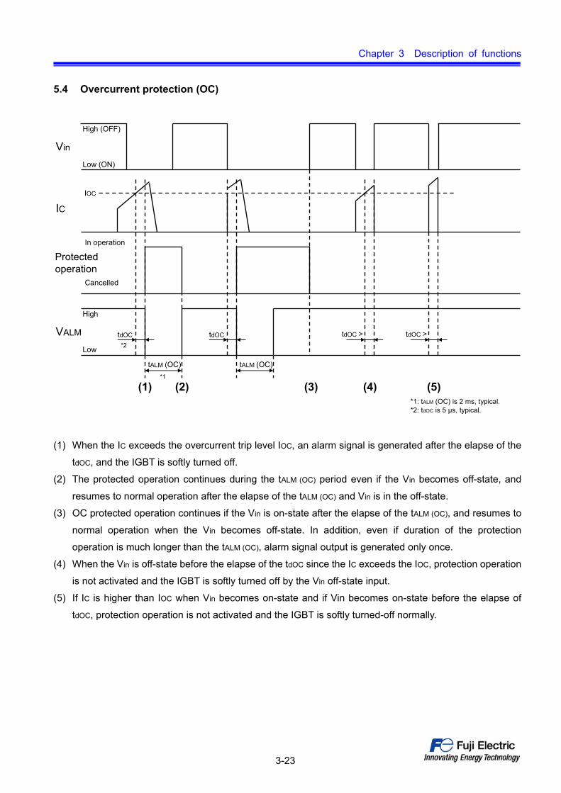
5.4 Overcurrent protection (OC)
Vin
IC
VALM
tALM (OC)
tdOC
tALM (OC)
tdOC tdOC >
IOC
Low (ON)
High (OFF)
High
Low
*1
*2
tdOC >
Protectedoperation
In operation
Cancelled
(1) (2) (3) (4) (5)*1: tALM (OC) is 2 ms, typical.*2: tdOC is 5 μs, typical.
(1) When the IC exceeds the overcurrent trip level IOC, an alarm signal is generated after the elapse of the
tdOC, and the IGBT is softly turned off.
(2) The protected operation continues during the tALM (OC) period even if the Vin becomes off-state, and
resumes to normal operation after the elapse of the tALM (OC) and Vin is in the off-state.
(3) OC protected operation continues if the Vin is on-state after the elapse of the tALM (OC), and resumes to
normal operation when the Vin becomes off-state. In addition, even if duration of the protection
operation is much longer than the tALM (OC), alarm signal output is generated only once.
(4) When the Vin is off-state before the elapse of the tdOC since the IC exceeds the IOC, protection operation
is not activated and the IGBT is softly turned off by the Vin off-state input.
(5) If IC is higher than IOC when Vin becomes on-state and if Vin becomes on-state before the elapse of
tdOC, protection operation is not activated and the IGBT is softly turned-off normally.

Chapter 3 Description of functions
3-24
5.5 Short-circuit protection (SC)
Vin
IC
VALM
tALM (OC)
tSC
tALM (OC)
tSC tSC > tSC >
ISC
IOC
Low (ON)
High (OFF)
High
Low
*1
*2
Protectedoperation
In operation
Cancelled
(1) (2) (3) (4) (5)*1: tALM (OC) is 2 ms, typical.*2: tSC is 2 μs, typical.
(1) If a load short-circuit occurs when normal Ic is flowing and if the IC exceeds ISC the peak current of the
IC is suppressed momentarily. After the elapse of tSC, an alarm signal is generated and the IGBT is
softly turned off.
(2) SC protectioed operation is stopped if the Vin is off-state after the elapse of the tALM (OC).
(3) When a load short-circuit occurs immediately after the IC is flowing and if the IC exceeds ISC the peak
current is suppressed momentarily. After the elapse of tSC an alarm is generated and the IGBT is softly
turned off.
(4) SC protection operation continues if the Vin is on-state even after the elapse of the tALM (OC). SC
protection operation is stopped when a Vin signal becomes off-state. In addition, even if duration of the
protection operation is much longer than the tALM (OC), alarm output is generated only once.
(5) When a load short-circuit occurs immediately after the IC began to flow and the IC peak is suppressed
momentarily as soon as the IC exceeds the ISC. If the Vin becomes off-state before the elapse of the tSC
the SC protection operation is not activated and the IGBT is softly turned off normally.
(6) When a load short-circuit occurs immediately after the IC began to flow, and the IC peak is suppressed
momentarily when the IC exceeds the ISC. If the Vin becomes off-state before the elapse of the tSC, the
SC protection operation is not activated and the IGBT is softly turned off normally.
Chapter 3 Description of functions
3-25
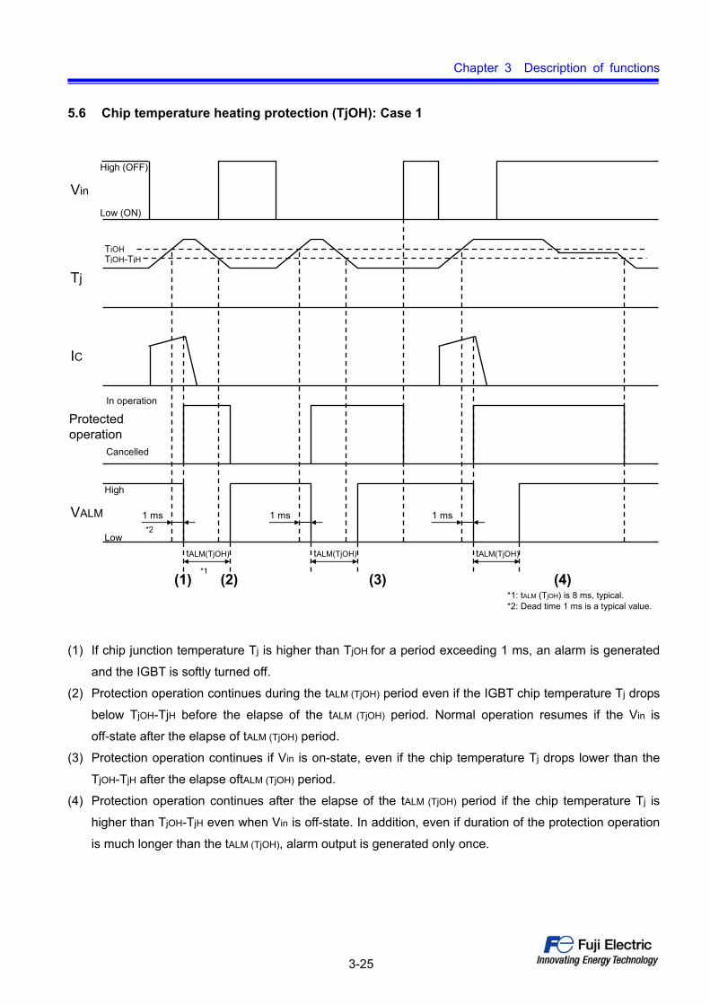
5.6 Chip temperature heating protection (TjOH): Case 1
Vin
IC
VALM
tALM(TjOH)
1 ms
TjOHTjOH-TjH
tALM(TjOH)
1 ms
Tj
Low (ON)
High (OFF)
High
Low
tALM(TjOH)
1 ms
*2
*1
Protectedoperation
In operation
Cancelled
(1) (2) (3) (4)*1: tALM (TjOH) is 8 ms, typical.*2: Dead time 1 ms is a typical value.
(1) If chip junction temperature Tj is higher than TjOH for a period exceeding 1 ms, an alarm is generated
and the IGBT is softly turned off.
(2) Protection operation continues during the tALM (TjOH) period even if the IGBT chip temperature Tj drops
below TjOH-TjH before the elapse of the tALM (TjOH) period. Normal operation resumes if the Vin is
off-state after the elapse of tALM (TjOH) period.
(3) Protection operation continues if Vin is on-state, even if the chip temperature Tj drops lower than the
TjOH-TjH after the elapse oftALM (TjOH) period.
(4) Protection operation continues after the elapse of the tALM (TjOH) period if the chip temperature Tj is
higher than TjOH-TjH even when Vin is off-state. In addition, even if duration of the protection operation
is much longer than the tALM (TjOH), alarm output is generated only once.

Chapter 3 Description of functions
3-26
5.7 Chip temperature heating protection (TjOH): Case 2
2.5 μs <1 ms >1 ms >
Vin
IC
VALM
tALM (TjOH)
1 ms
TjOHTjOH-TjH
tALM (TjOH)
1 ms
Tj
Low (ON)
High (OFF)
High
Low*2
Protectedoperation
In operation
Cancelled
(1) (2) (3)*1: tALM (TjOH) is 8 ms, typical.*2: Dead time 1 ms is a typical value.
*1
(1) Protection operation is not activated if the Tj drops lower than the TjOH within 1 ms since Tj exceeds
TjOH, regardless of whether the Vin is on or off.
(2) The TjOH detection timer of which duration is 1 ms is reset if Tj has been kept lower than the TjOH-TjH for
longer than 2.5 µs after the Tj exceeds the TjOH.

Chapter 3 Description of functions
3-27
5.8 Case where protective functions operated compositely
VCC
VUV+VHVUV
VALM
tALM (UV)
High
Low
Vin
High (OFF)
Low (ON)
20 μs1 ms
tALM (TjOH)
TjOHTjOH-TjH
Tj
1 ms
tALM (TjOH)
IC
*3
Protectedoperation
In operation
Cancelled
*1 *2
(1) (2) (3) (4) (5) (6) (7)*1: tALM (TjOH) is 8 ms, typical.*2: tALM (UV) is 4 ms, typical.
*3: Dead time 1 ms is a typical value.*4: Dead time 20 μs is a typical value.
*4
(1) When an IGBT junction temperature Tj exceeds the TjOH for 1 ms continuously, an alarm is generated
and the IGBT is softly turned off.
(2) If the VCC drops lower than the VUV before the elapse of the tALM (TjOH) period, an alarm output of UV
protection is cancelled because protected operation of the TjOH is continuing.
(3) Protection operation stops after the elapse of tALM (TjOH) period if Vin is off-state and chip temperature Tj
drops less than TjOH-TjH.
(4) An alarm signal is generated and the IGBT is softly turned off if the IGBT chip temperature Tj
continuously exceeds of TjOH for 1 ms.
(5) Similar to the case (2), alarm output by VUV is stopped while protection operation of the tALM (TjOH) is
continued.

Chapter 3 Description of functions
3-28
(6) Protected operation stops after the elapse of tALM (TjOH) period if Vin is off-state and the chip
temperature Tj drops lower than the TjOH-TjH. At this time VCC is kept lower than the VUV for 20 µs after
the stop of protective functions by TjOH, an alarm is generated by the VUV again and the UV protected
operation is activated.
(7) Protected operation stops after the elapse of tALM (UV) period if Vin is off-state and VCC is higher than
VUV + VH.
5.9 Multiple alarm outputs from lower arm by control power supply under voltage protection
(UV) (excluding P629)
Each of three (or four for brake built-in type)
IGBTs have independent control ICs, but the
alarm outputs is a common output for lower arm
control ICs. Therefore, there are some cases
when several alarm outputs are generated
because of distribution of protected operation
level of the control ICs. If dv/dt of VUV is less
than 0.5 V/ms in the vicinity of VCC, there is a
possibility of alarm output such as shown in the
figure right. (This is not an abnormal
phenomenon.)
VCC
VUV+VHVUV (IC_A)
VALM
*1: tALM (UV) is 4 ms, typical.
High
Low
Lower arm IC_ALower arm IC_B
Lower arm IC_C
tALM (UV) *1
VUV (IC_B)VUV (IC_C)

– Chapter 4 –
Typical application circuits
4-1
Table of Contents Page
1 Typical application circuits ............................................ 4-2
2 Important remarks ............................................ 4-6
3 Optocoupler peripheral circuits ............................................ 4-9
4 Connector ............................................ 4-11

Chapter 4 Typical application circuits
4-2
1 Typical application circuits
Figure 4-1 shows typical application circuits of P629.
Figure 4-1 Typical application circuits of P629
5V 0.1uF20kΩ
10μF
P
U
V
W
N
IPM
VccU
GNDU
15V
VinU
VccV
GNDV
VinV
VccW
GNDW
VinW
Vcc
GND
VinX
VinY
VinZ
ALM
Input signal
Alarm output
47μF
10nF

Chapter 4 Typical application circuits
4-3
Figure 4-2 shows typical application circuits of P626.
Figure 4-2 Typical application circuits of P626
(a) Where upper phase alarm is used (b) Where upper phase alarm is not used
5V
P
U
V
W
N
IPM
VccU
GNDU
15V
VinU
VccV
GNDV
VinV
VccW
GNDW
VinW
Vcc
GND
VinX
VinY
VinZ
ALM
Input signal
Alarm output
ALMU
5V
5V
ALMV
ALMW
5V
5V 0.1uF
20kΩ
10μF
P
U
V
W
N
IPM
VccU
GNDU
15V
VinU
VccV
GNDV
VinV
VccW
GNDW
VinW
Vcc
GND
VinX
VinY
VinZ
VinDB
ALM
Input signal
Alarm output
ALMU
ALMV
ALMW
VinDB
47μF 47μF
10nF
0.1uF
20kΩ
10μF
10nF
10nFAlarm output
(No Contact)(No Contact)

Chapter 4 Typical application circuits
4-4
Figure 4-3 shows typical application circuits of P630, P631 and P636 with built-in brake type.
Figure 4-3 Typical application circuits of P630, P631 and P636 with brake circuit
5V
P
U
V
W
B
N
IPM
VccU
GNDU
15V
VinU
VccV
GNDV
VinV
VccW
GNDW
VinW
Vcc
GND
VinX
VinY
VinZ
VinDB
ALM
Input signal
Alarm output
Brake resistor
ALMU
5V
5V
ALMV
ALMW
5V
5V
P
U
V
W
B
N
IPM
VccU
GNDU
15V
VinU
VccV
GNDV
VinV
VccW
GNDW
VinW
Vcc
GND
VinX
VinY
VinZ
VinDB
ALM
Input signal
Alarm output
Brake resistor
ALMU
ALMV
ALMW
47μF 47μF
10nFAlarm output
0.1uF
20kΩ
10μF
10nF
0.1uF
20kΩ
10μF
10nF
(a) Where upper phase alarm is used (b) Where upper phase alarm is not used
Chapter 4 Typical application circuits
4-5
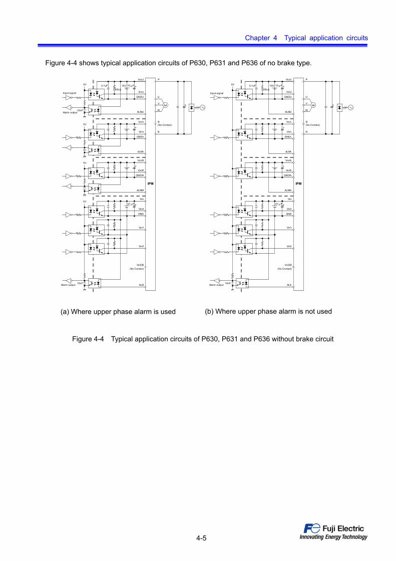
Figure 4-4 shows typical application circuits of P630, P631 and P636 of no brake type.
Figure 4-4 Typical application circuits of P630, P631 and P636 without brake circuit
5V
P
U
V
W
B
N
IPM
VccU
GNDU
15V
VinU
VccV
GNDV
VinV
VccW
GNDW
VinW
Vcc
GND
VinX
VinY
VinZ
ALM
Input signal
Alarm output
ALMU
5V
5V
ALMV
ALMW
5V
5V 0.1uF
20kΩ
10μF
P
U
V
W
N
IPM
VccU
GNDU
15V
VinU
VccV
GNDV
VinV
VccW
GNDW
VinW
Vcc
GND
VinX
VinY
VinZ
VinDB
ALM
Input signal
Alarm output
ALMU
ALMV
ALMW
VinDB
B
47μF 47μF
0.1uF
20kΩ
10μF
10nFAlarm output
10nF 10nF
(No Contact) (No Contact)
(No Contact)(No Contact)
(a) Where upper phase alarm is used (b) Where upper phase alarm is not used

Chapter 4 Typical application circuits
4-6
2 Important remarks
2.1 Control power supply units
Four isolated power supply units; three for the upper arm and one for the lower arm are needed as shown
in the application circuit examples. If a readymade power supply unit is used, do not connect the output
GND terminals of the power supply unit. If the GND of the output side is connected to the + or − terminals, it
may cause a failure of the system because each power supply unit is connected to the ground of input side
of the power supply unit. Furthermore, reduce stray capacitance (floating capacitance) between the power
supply units and the Earth ground as much as possible.
Furthermore, please use a power supply unit which has enough capability to supply ICC with low output
power fluctuation.
2.2 Structural insulation between four power supply units (input portion connector and PCB)
The four power units and the main power supply unit have to be insulated from each other. A sufficient
insulation air gap distance is required (2 mm or longer is recommended) because a high dv/dt is applied to
the insulation distance during IGBT switching.
2.3 GND connection
Do not connect the control terminal GND U to the main terminals U, control terminal GND V to main
terminals V, control terminal GND W to main terminal W, control terminal GND to main terminal N (N1 and
N2 in case of P631). If these terminals are connected, it might cause a malfunction.
2.4 External capacitors for control power supply
Capacitors of 10 μF (47 μF) and 0.1 μF, which are connected to each power supply unit shown in typical
application circuits are not used for smoothing the output voltage of the control power supply units but are
used for reduction of the wiring impedance from the power supply unit to the IPM. Additional capacitors for
smoothing the voltage are required.
Furthermore, these external capacitors should be connected to the IPM terminals or optocoupler
terminals as short as possible because transient variation occurs by the wiring impedance between the
capacitors and control circuits.
Also, an electrolytic capacitor which has a low impedance and god frequency characteristics is
recommended. In addition, it is recommended to connect a film capacitor which has good frequency
characteristics in parallel.

Chapter 4 Typical application circuits
4-7
2.5 Alarm circuit
The alarm terminal has a 1.3 kΩ internal resistor in series, so that an optocoupler can be connected to
the terminal directly without an external resistor. The wiring distance between the optocoupler and the IPM
should be as short as possible. Also the pattern layout should be designed to minimize the floating
capacitance between the primary side and the secondary side of the optocoupler. Because of the potential
of the secondary side of the optocoupler it may fluctuate due to high dv/dt. It is recommended that a 10nF
capacitor of is connected to the output terminal of the secondary side of the optocoupler as shown in Figure
4-4.
Furthermore, f upper side alarm outputs are not used, please connect the alarm output terminal to VCC as
shown in Figure 4-4 (b).
2.6 Pull-up of signal input terminal
Connect the control signal input terminals to Vcc through a 20 kΩ pull-up resistor. Furthermore, unused
input terminals also have to be pulled up through a 20 kΩ resistor. If these terminals are not pulled up, an
under voltage protection is activated during the starting up so that no ON operation is possible.
2.7 Connection in case there is an unused phase
If there is an unused phase such as the case when a 6in1 IPM (no brake type) is used in single phase or
a 7in1 IPM (brake built-in type) is used without using B-phase, please supply a control voltage to these
unused phase and connect the input/alarm terminals of the phase to VCC so that it will stabilize the potential
of these terminals.
2.8 Handling of unconnected terminals (no contact terminals)
Unconnected terminals (no contact terminals) are not connected to the internal of the IPM. These
terminals are insulated from other terminals. There is no need of special treatment such as potential
stabilization.
Furthermore, guide pins should also not be connected to the internal of the IPM.
2.9 Snubbers
Connect snubber circuits between P and N terminals directly and as short as possible.
For P631 package which has two P/N terminals, it is effective for surge voltage reduction to connect
snubber circuits to the P1-N1 and P2-N2 terminals. Do not connect snubber circuits across the two
terminals such as P1-N2 and P2-N1 because it may cause a malfunction.
2.10 Grounding capacitor
Please connect about 4500 pF capacitors between each AC input line and Earth ground to prevent a
noise from the AC input line to the system.

Chapter 4 Typical application circuits
4-8
2.11 Input circuit of IPM
There is a constant current circuit in the input part of the IPM as shown in Figure 4-5 and constant current
of lin = 0.15 mA or lin = 0.65 mA flows at that timing shown in Figure 4-5.The current of the secondary side
of optocoupler is the sum of the constant current Iin and the current through a pull-up resistor IR. Therefore
it is necessary to decide the current of primary side of optocoupler IF so that enough current flows in the
secondary side of optocoupler. If the IF is insufficient, there is a possibility that a malfunction arises on the
secondary side.
SW1-1 OFFSW1-2 ONSW2 OFF
0.15 mA outflows from VinIPM Vin
About 5 us
SW1-1 OFFSW1-2 OFFSW2 ON
SW1-1 ONSW1-2 OFFSW2 OFF
SW1-1 OFFSW1-2 ONSW2 OFF
0.65 mA outflows from Vin
SW 1-1
SW 2
Vin
Vcc
GND
IPM
200 KΩ
SW 1-2
Constantcurrent circuit
(0.15 mA)
Vcc = 15 V
Pull-upresistanceR
Photocoupler
IR Iin
I
Constantcurrent circuit(0.65 mA)
Constantcurrent circuit(0.05 mA)
* The operation duration of constant current circuit (0.65 mA) is the length of time until Vin reaches VCC,
and the maximum length about 5 μs.
Figure 4-5 IPM input circuit and constant current operation timing

Chapter 4 Typical application circuits
4-9
3 Optocoupler peripheral circuits
3.1 Control input Optocoupler
3.1.1 Optocoupler rating
Use an optocoupler that satisfies the characteristics indicated below:
• CMH = CML > 15 kV/μs or 10 kV/μs
• tpHL = tpLH < 0.8 μs
• tpLH − tpHL = −0.4 to 0.9 μs
• CTR > 15%
Example: HCPL-4504 made by Avago Technologies
TLP759 (IGM) made by Toshiba
Pay attention to safety standards such as UL and VDE.
The reliability and characteristics of these optocouplers are not guaranteed by Fuji Electric.
3.1.2 Primary side limit resistance
The current limiting resistor on the primary side should be selected to have an ability to flow a sufficient
current on the secondary side. Also, an age-related deterioration of CTR of the optocoupler should be
considered in the design of the current limiting resistor.
3.1.3 Wiring between optocoupler and IPM
The wiring distance between the optocoupler and the IPM should be short as much as possible to reduce
the impedance of the line. The primary line and secondary line of the optocoupler should be kept away from
each other to reduce the floating capacitance. High dv/dt is applied between the primary side and the
secondary side.

Chapter 4 Typical application circuits
4-10
3.1.4 Optocoupler drive circuit
A noise current flows through the floating capacitance between the primary side and the secondary side
of the optocoupler due to the high dv/dt that is generated inside or outside of the IPM. The dv/dt tolerance
also varies by the optocoupler drive circuit. Good/bad examples of the optocoupler driving circuits are
shown in Figures 4-6. As the opotocoupler input is connected in low impedance in these good examples,
malfunction caused by noise current hardly occurs. Please contact to the optocoupler manufacturer
regarding details of the optocouplers.
Good example: Totem pole output IC Current limit resistance on cathode side of photodiode
Bad example: Open collector
Bad example: Current limit resistance on anode side of photodiode
Good example: Diodes A and K are shorted between transistors C and E (Case that is particularly strong against photocoupler off)
Figure 4-6 Optocoupler input circuits

Chapter 4 Typical application circuits
4-11
3.2 Alarm output optocoupler
3.2.1 Optocoupler ratings
A general-purpose optocoupler can be use but an optocoupler of the following characteristics is
recommended:
• 100% < CTR < 300%
• Single channel type
Example: TLP781-1-GR rank or TLP785-1-GR rank made by Toshiba
Pay attention to safety standards such as UL and VDE also.
The reliability and characteristics of the optocouplers indicated above are not guaranteed by Fuji Electric.
3.2.2 Input current limiting resistance
A current limiting resistor for input side diode of optocoupler is built in the IPM. The resistance RALM = 1.3
kΩ, and IF is about 10 mA when the optocoupler is connected to VCC = 15 V. An external current limiting
resistor is not required.
If large current Iout > 10 mA is required for the optocoupler output side, it is necessary to increase the
optocoupler’s CTR value to achieve the required level.
3.2.3 Wiring between optocoupler and IPM
Note that high dv/dt is applied to the optocoupler for alarm output, please take care as same as to
Section 3.1.3.
4 Connector
Connectors that conform to the shape of control terminals of V-IPM are available on the market.
For P630: MA49-19S-2.54DSA and MA49-19S-2.54DSA (01) made by Hirose Electric
For P631: MDF7-25S-2.54DSA made by Hirose Electric
Furthermore, please contact the connector manufacturer for the details of reliability and use of these
connectors.
Please note that the reliability and the characteristics of these connectors are not guaranteed by Fuji
Electric.

– Chapter 5 –
Cooling Design
5-1
Table of Contents Page
1 Method for selection of heat sink ............................................ 5-2
2 Important remarks for selection of a heat sink ............................................ 5-2
3 How to mount the IPM ............................................ 5-3

Chapter 5 Heat dissipation design
5-2
1 Guidelines for heat sink selection
• To safely operate the IGBT, it is necessary that the junction temperature Tj should not exceed Tjmax.
Carry out thermal design having sufficient margins so that the junction temperature Tj never exceeds the
Tjmax also on occurrence of disorder such as overload.
• There is a risk of thermal breakdown, if the IGBT is operated at temperature above the Tjmax.
Although the TjOH protected function in the IPM activates when the junction temperature exceeds the
Tjmax, however, there is a possibility that the protection cannot work if the temperature rises rapidly.
Also pay attention to the FWD so that the Tjmax should not be exceeded, same case for the IGBT.
• The heat sink temperature should be measured just below the center of the chip.
Please refer to the IPM specification sheet for the chip layout drawing.
In addition, please consider the following documents regarding to the design for your reference.
[IGBT Module Application Manual RH984b]
• How to calculate the occurred loss
• How to select a heat sink
• How to mount IPM to a heat sink
• Troubleshooting
2 Notice for heat sink selection
Although a guideline for heat sink selection is described in the IGBT Module Application Manual
(RH984b), please pay attention to the following recommendations as well.
2.1 Flatness of the heat sink surface
It is recommended that flatness of the heat sink surface is less than 50 μm per 100 mm between screw
mounting points and the surface roughness is less than 10 μm.
If the heat sink surface is concave or convex, the contact thermal resistance (Rth(c-f)) will be increased.
[Reason]
• Concave: A gap appears between the heat sink
surface and the bottom of the IPM, and the heat
transfer performance becomes worse (contact
thermal resistance Rth(c-f) increases).
• Convex (larger than +50 μm): The copper base of
the IPM is deformed and there is a possibility of a
generation of cracks on the internal insulated
board by the mechanical stress.
Figure 5-1 Flatness of heat sink surface
Compound coated face
Component
100 mm
+−
Between screw mounting points

Chapter 5 Heat dissipation design
5-3
3 Mounting instruction of the IPM
3.1 Layout of IPMs on a heat sink
The thermal resistance varies depending on the IPM mounting position. Please note the following
matters:
• When an IPM is mounted to a heat sink, it is recommended to place the IPM on the center of the heat
sink to maximize the usage of the heat sink.
• When multiple IPMs are mounted to a single heat sink, the IPMs location and layout should be designed
with their generated losses. Allocate the largest area to the IPM which generates largest loss.
3.2 Application of thermal grease
To reduce the contact thermal resistance, apply thermal grease between the IPM and heat sink mounting
surface.
Use of a stencil mask and use of a roller are available in general as methods for application of thermal
grease.
The purpose of the thermal grease is to promote heat transmission to the heat sink, but the grease has a
limited thermal capacity. If the thickness of thermal grease is larger than the appropriate thickness, the
grease layer prevents the heat transfer from the IPM to the heat sink and the junction temperature will be
increased. On the other hand, if the thermal grease thickness is less than the appropriate thickness, such
as a void area, a gap or space may be caused between the heat sink and the IPM. This may cause an
increasee of the contact thermal resistance. Therefore thermal grease should be applied in appropriate
thickness.
If the thermal grease thickness is inadequate, the thermal dissipation of heat becomes worse, and there
is a possibility of breakdown in the worst case due to the excess of the junction temperature Tjmax.
Application of thermal grease using a stencil mask is recommended so that uniform thickness can be
achieved.
Figure 5-2 shows an example of a thermal grease application using a stencil mask. The basis of this
method is applying specified weight of thermal grease to the metallic base of the IPM using a stencil mask.
It is possible to achieve a uniform thickness of thermal grease by mounting the IPM with thermal grease to
the heat sink and tightening screws with recommended torque for each product. Fuji Electric can provide
recommended stencil mask designs upon request of customers.

Chapter 5 Heat dissipation design
5-4
Figure 5-2 Outline of a thermal grease application method

Chapter 5 Heat dissipation design
5-5
The required thermal grease weight is given by the following equation by assuming uniform thermal
grease thickness:
Thermal grease
weight (g) x 10-4
=
Thermal grease thickness (μm) x IPM base area (cm2)
× Thermal grease density (g/cm3)
Calculate the thermal grease weight that corresponds to the required thermal grease thickness from this
equation, and apply the thermal grease. The recommended thermal grease thickness after spreading of
thermal grease is 100 μm. Also please note that the optimum thermal grease thickness varies by the
characteristics of the used thermal grease and application method.
Table 5-1 shows the footprint area of IPMs.
Table 5-1 Back Base plate area of IPM
Package Back side base
area (cm2)
P629 21.71
P626 22.77
P630 55.67
P631 141.24
P636 41.17
Table 5-2 Shows recommended thermal greases (typical)
Table 5-2 Typical thermal greases
Type Manufacturer
G746 Shin-Etsu Chemical Co., Ltd.
TG221 Nippon Data Material Co., Ltd.
SC102 Dow Corning Toray Co., Ltd.
YG6260 Momentive Performance Materials Inc.
P12 Wacker Chemie
HTC ELECTROLUBE
The list of thermal greases shown above is based on the information at the time of issuance of this
Application Manual. Please contact these manufacturers for details of these thermal greases.

Chapter 5 Heat dissipation design
5-6
3.4 Screw tightening
Figure 5-3 shows screw-tightening procedures for mounting an IPM to a heat sink. It is recommended to
tighten all screws with specified tightening torque.
The specified tightening torque is described in the specification. If the screw tightening torque is
insufficient, there is a possibility of increasing the contact thermal resistance or loosing screws during
operation. If the tightening torque is excessive, on the other hand, the case would be damaged.
押し出し方向
ヒートシンク
① ネジ位置 ② モジュール
Torque Order
1st time (initial tightening)
2nd time (permanent tightening)
1/3 of specified torque
100% of specified torque
(1) → (2)
(2) → (1)
(1) Case of IPM of 2-point mounting type
押し出し方向
ヒートシンク ① ③
ネジ位置 モジュール
④ ②
Torque Order
1st time (initial tightening)
2nd time (permanent tightening)
1/3 of specified torque
100% of specified torque
(1) → (2) → (3) → (4)
(4) → (3) → (2) → (1)
(2) Case of IPM of 4-point mounting type
Figure 5-3 IPM mounting method
Extruding direction
Module
Heat sink
Screw positions
Extruding direction
Module
Heat sink
Screw positions

Chapter 5 Heat dissipation design
5-7
3.5 IPM mounting direction
When an IPM is mounted on an extruded heat sink, it is recommended that the IPM is mounted in parallel
to the extrusion direction as shown in Figure 5-3. This purpose is to reduce the influence of heat sink
deformation.
3.6 Verification of chip temperature
After selecting a heat sink and IPM mounting position is decided, measure the temperature at various
points on case (Tc), heat sink (Tf) and junction temperature (Tj).
Figure 5-4 shows an example of measuring method for an accurate measurement of case temperature
(Tc). Please measure the case temperature just below the chip center. The chip location is described in the
specification.
Please verify that the chip junction temperature does not exceed Tjmax and the thermal design meets
required life time of the system.
Heat sink
Tc (just below the chip)
Tf (just below the chip)
Chip
Base
CompoundThermocouple
Groove machining
Figure 5-4 Measuring the case temperature

– Chapter 6 –
Precautions for use
6-1
Table of Contents Page
1 Main power supply ............................................ 6-2
2 Control power supply ............................................ 6-3
3 Protective functions ............................................ 6-4
4 Power Cycling Capability ............................................ 6-5
5 Others ............................................ 6-6

Chapter 6 Precautions for use
6-2
1 Main power supply
1.1 Voltage range
• The collector and emitter terminal voltage (=VCES) should never exceed the absolute maximum rated
voltage (600 V-series = 600 V, 1200 V-series = 1200 V).
• In order to keep the maximum surge voltage between all terminals within the rated voltage during the
switching, connect the IPM and other components as short as possible to each other and connect a
snubber capacitor between P and N terminals.
Between all terminals means as follows:
P629, P626, P630 (6in1), P636 (6in1): [P-(U, V, W), (U, V, W)-N]
P630 (7in1), P636 (7in1): [P-(U, V, W, B), (U, V, W, B)-N]
P631 (6in1): [P1-(U, V, W), P2-(U, V, W), (U, V, W)-N1, (U, V, W)-N2]
P631 (7in1): [P1-(U, V, W, B), P2-(U, V, W, B), (U, V, W, B)-N1, (U, V, W, B)-N2]
• In case of P631, connect the dc bus power supply between the P1 and N1 or between the P2 and N2.
Don’t connect cross-multiply connections such as between the P1 and N2 and between the P2 and N1. It
might cause a false operation. It is effective to connect snubber capacitors to both terminals between the
P1/N1 and between the P2 / N2 terminals to suppress the surge voltage.
1.2 Noise protection
• The V-IPM series has a tolerance against exogenous noise. However, there is a possibility of false
operation or breakdown of the V-IPM by exogenous noise depending on the kind and intensity of the
noise. It is recommended to implement other protections against the noise applied to the IPM.
1.2.1 Protection against external noise
• Take countermeasures such as installing a noise filter along the AC line and strengthening of insulating
grounding.
• Add a capacitor of <100 pF between signal input line and signal GND of every phase, as necessary.
• When the excessive noise voltage increases on the alarm terminal, it may become a false output of the
alarm signal. Please connect 0.2 kΩ to 1 kΩ resistor in series to the alarm terminal as needed. Please
choose a most suitable resistance level in consideration of CTR of the optocoupler on this occasion.
• Connect a grounding capacitor of about 4700 pF between each line of 3 phases of AC input and ground,
for preventing entry of noise through the AC line.
• Insert an arrester against lightning surge.
1.2.2 Protection against the internal noise from the IPM
• Outside of rectifier: Apply the same countermeasures as Section 1.2.1.
• Inside of rectifier: Add snubber capacitors or similar circuit to the P/N line. (Particularly in case multiple
inverters are connected to one rectifying converter)
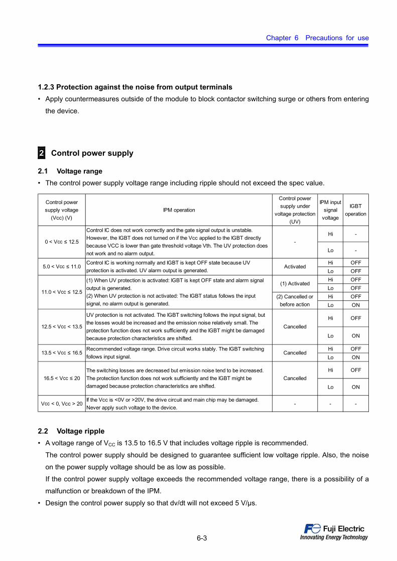
Chapter 6 Precautions for use
6-3
1.2.3 Protection against the noise from output terminals
• Apply countermeasures outside of the module to block contactor switching surge or others from entering
the device.
2 Control power supply
2.1 Voltage range
• The control power supply voltage range including ripple should not exceed the spec value.
Control powersupply voltage
(Vcc) (V)IPM operation
Control powersupply under
voltage protection(UV)
IPM inputsignal
voltage
IGBToperation
Hi -
Lo -
Hi OFFLo OFFHi OFFLo OFFHi OFFLo ON
Hi OFF
Lo ON
Hi OFFLo ON
Hi OFF
Lo ON
V < 0, Vcc > 20If the Vcc is <0V or >20V, the drive circuit and main chip may be damaged.Never apply such voltage to the device.
- - -
0 < V ≤ 12.5
Control IC does not work correctly and the gate signal output is unstable.However, the IGBT does not turned on if the Vcc applied to the IGBT directlybecause VCC is lower than gate threshold voltage Vth. The UV protection doesnot work and no alarm output.
-
5.0 < V ≤ 11.0Control IC is working normally and IGBT is kept OFF state because UVprotection is activated. UV alarm output is generated.
Activated
16.5 < V ≤ 20The switching losses are decreased but emission noise tend to be increased.The protection function does not work sufficiently and the IGBT might bedamaged because protection characteristics are shifted.
Cancelled
13.5 < V ≤ 16.5Recommended voltage range. Drive circuit works stably. The IGBT switchingfollows input signal.
Cancelled
12.5 < V < 13.5
UV protection is not activated. The IGBT switching follows the input signal, butthe losses would be increased and the emission noise relatively small. Theprotection function does not work sufficiently and the IGBT might be damagedbecause protection characteristics are shifted.
Cancelled
11.0 < V ≤ 12.5
(1) When UV protection is activated: IGBT is kept OFF state and alarm signaloutput is generated.(2) When UV protection is not activated: The IGBT status follows the inputsignal, no alarm output is generated.
(1) Activated
(2) Cancelled orbefore action
2.2 Voltage ripple
• A voltage range of VCC is 13.5 to 16.5 V that includes voltage ripple is recommended.
The control power supply should be designed to guarantee sufficient low voltage ripple. Also, the noise
on the power supply voltage should be as low as possible.
If the control power supply voltage exceeds the recommended voltage range, there is a possibility of a
malfunction or breakdown of the IPM.
• Design the control power supply so that dv/dt will not exceed 5 V/μs.

Chapter 6 Precautions for use
6-4
Additionally, it is recommended that variation of the power supply voltage does not exceed ±10%.
2.3 Power supply startup/shutdown sequence
• Make sure that the main power supply voltage Vcc is within the recommended voltage range, before
applying this voltage to the main power supply terminals (P-N terminal).
• Shutdown the voltage supply (Vcc) and disconnect the P-N terminals of the IPM then.
If VCC is applied to the P-N terminals before the voltage reaches the recommended voltage range there
may happen a malfunction due to exogenous noise and the chip might be damaged. Same case occurs if
low voltage of VCC remains before disconnecting P-N terminals.
2.4 Alarm output during startup/shutdown of power supply
• An alarm signal (typ = 4 ms) is generated when the power supply voltage is lower than UV protection
level during startup of the power supply.
The alarm signal is stopped after typ = 4 ms but the input signal is ignored unless the root cause of the
protection is settled. An input signal is accepted when all the protection operation functions are not
activated (dissolving of protection factor, elapse of tALM and input signal OFF). The drive control circuit
should be designed to output gate signals after the period of alarm signal output.
• Also note that an alarm signal is generated during VCC shutdown.
• See Chapter 3, section 5 [Timing chart] for considering the timing chart.
2.5 Notes for the design of control circuit
• The control circuit should be well-designed to have enough capability to provide a specified consumption
current (Icc).
• Minimize the length of the wiring between the optocoupler and the IPM as well as the pattern layout
should be designed to minimize the floating capacitance between the primary side and the secondary
side of the optocoupler.
• Add a capacitor between Vcc and GND for high-speed optocouplers.
• Use a high-speed optocoupler of tpHL, tpLH ≤ 0.8 µs and of high CMR type for the control signal input
circuit.
• Use a low-speed optocoupler of CTR ≥ 100% for the alarm output circuit.
• The four power supply units for the power supply control Vcc have to be isolated. Also, it is
recommended to connect a capacitor which has a good frequency response characteristic on the output
terminal of each power supply unit to suppress transient voltage variation.
• Note that if a capacitor is connected between an input terminal and GND, the response time of the
optocoupler becomes slow.
• The optocoupler primary side current IF should have enough capability in consideration of CTR of the
used optocoupler. To reduce the influence of noise, the pull-up resistance on the optocoupler secondary

Chapter 6 Precautions for use
6-5
side should be small.
As described in Chapter 4 [Typical application circuits], it is necessary to design the IF on the optocoupler
primary side so that the constant current through the pull-up resistance IR can flow to the secondary
side. . If the IF is insufficient, there is a possibility of a malfunction on the secondary side circuit.
Also, the resistance of current limiting resistor on the primary side of the optocoupler should be designed
in consideration of a life time of the optocoupler.
3 Protective functions
• An alarm output function varies depending on the package. Check protective functions of your IPM by
referring to Chapter 3.1 [List of functions].
3.1 Protected operation in general
3.1.1 Range of protection
• The protective functions of the IPM deal with non-repeated abnormal phenomena. Avoid a situation of
repetitive occurrence of abnormal phenomena.
• Overcurrent and short-circuit protections are guaranteed under the condition of control power supply
voltage 13.5 to 16.5 V and main power supply voltage 200 to 400 V (600 V-series) or 400 to 800 V
(1200 V-series).
3.1.2 Action on occurrence of alarm output
• When an alarm signal is generated the input signal to the IPM stops and shutdown the system
immediately.
• The IPM protective functions protect the IPM against abnormal phenomena but they are not able to
eliminate the causes. Please dissolve the abnormal phenomena by finding the root cause and then
restart the system.
• When an abnormal phenomenon is detected in the upper arm, the IGBT of the detected phase is only
turned off and an alarm output is generated from the same phase (excluding P629). Switching of other
phases is permitted at this time. On the other hand, when an abnormal phenomenon is detected in the
lower arm all the IGBTs of the lower arm (+ brake unit) is turned off regardless of the phase and an alarm
is generated from the lower arm. Switching of all phases of the upper arm is permitted at this time.
3.2 Precautions for protected operation
3.2.1 Overcurrent (OC)
• When overcurrent continues longer than 5 µs (tdOC), it is judged as being in the OC condition and the
IGBT is turned off softly. An alarm output signal is generated.
If current descend below the trip level within the tdOC period the OC protection is not activated and the

Chapter 6 Precautions for use
6-6
IGBT is turned-off normally (hard turn-off).
• P629 does not have an alarm output on the upper side arms but the OC protection does work and the
IGBT is turned off softly.
3.2.2 Short-circuit (SC)
• When short-circuit current continues longer than 2 µs (tdsc) it is judged as being in the SC condition and
the IGBT is turned off softly. An alarm signal output is generated.
If short-circuit current descends below the trip level within the tdsc period, the SC protection does not
work and soft turn-off is not applied to the IGBT.
• P629 does not have an alarm output on the upper arms but the SC protection does work and soft turn-off
is applied to the IGBT.
3.2.3 Ground short circuit
• When ground-fault current flows to the IGBT of the lower arm longer than the dead time tdOC or tdsc
the OC (SC) protection is activated and an alarm signal is generated.
• When the ground-fault current flows to the IGBT of the upper arm longer than tdOC or tdsc the OC (SC)
protection is activated but the alarm signal output varies by the package.
P629: The upper arm is protected by the OC (SC) function without alarm output.
P626, P630, P631, P636: The upper arm is protected by the OC (SC) function and an alarm signal is
generated.
3.2.4 Booting under short-circuit or ground-fault status
• Because the OC or SC protection involves a dead time (tdOC or tdsc), the protected operation is not
activated when the input signal pulse width is shorter than the dead time. Especially when the IPM is
booted under the load short-circuit condition the input signal pulse width is shorter than the dead time for
a long time (tens of mill seconds). The chip temperature rapidly increases because the protection
function doesn’t work. In this case, even though the chip over heat protection (TjOH) works against the
increase of the chip temperature, the response time of TjOH is about 1ms. Therefore, there is a
possibility of damaging the chip by over temperature since the protection is not on time.
3.3 Chip overheat protection
• Chip overheat protection (TjOH) is built in every IGBT including brake unit. The TjOH interacts when a
chip is abnormally heated up. Since the V-IPM does not have a case overheat protection, TjOH
protection does not activate when Tj is lower than the trip level even if Tc reveals an abnormal
temperature. Please implement another protection for Tc overheating as required.
3.4 Protection of FWD
• FWDs don’t have protective functions (overcurrent, overheat protection).

Chapter 6 Precautions for use
6-7
4 Power Cycling Capability
• The lifetime of semiconductor products is not unlimited. Note that thermal fatigue caused by temperature
rise/drop due to self-heating restricts the lifetime. If temperature rise and drop occur continuously the
reduction of the temperature variation amplitude is mandatory.
(1) ∆Tj power cycle capability: life time determined by junction temperature (Tj) change that arises in a
relatively short period and consequently a deterioration of wire connection on the chip surface is
possible.
Please refer to MT5Z02525 (P629, P626, P630, P631, P636) for the ∆Tj power cycling capability
curves.
(2) ∆Tc power cycle capability: life time determined by copper base plate temperature (Tc) change that
arises in a relatively long period and consequently a deterioration of solder layer between the DCB and
copper base can occur which is the main cause of the life time reduction).
Please refer to MT5Z02509 (P629, P626, P630) and MT5Z02569 (P630 low thermal resistance
version, P631, P636) for ∆Tc power cycling capability curves.
• Please refer to chapter 11 [Reliability of power modules] of Fuji IGBT Module Application Manual
(RH984b) in addition.
5 Others
5.1 Precautions for use and mounting procedure
(1) Please refer to the IPM specification in addition to this manual for usage and mounting procedure of
the IPM.
(2) Please install a fuse or circuit breaker of an adequate capacity between the input AC power line and
the system for stopping the spreading of damage when the IPM is failed.
(3) Designing a turn-off operation of the IGBT chip, please confirm that the turn-off current-voltage
operation track does not exceed the RBSOA specification.
(4) Please understand the product usage environment and check if the reliability of the IPM satisfies the
demand, before using the product. If the IPM is used beyond the spec, there is a possibility of failure
before the designed lifetime of the system.
(5) Please reduce the contact thermal resistance as much as possible between of the IPM and the heat
sink by applying thermal compound. (See Chapter 5, Section 3.)
(6) Please use appropriate length of screws. The package may be damaged if the screw length is longer
than the screw hole depth. (See Chapter 1, Section 6.)
(7) Tightening torque and heat sink flatness should be within the range of specified values.

Chapter 6 Precautions for use
6-8
Wrong handling may cause an insulation breakdown. (See Chapter 5, Section 2.)
(8) Do not apply excessive weight to the IPM.
Don’t apply deforming forces to the lid. If pushing force was applied to the lid, the internal circuit might
be damaged. If pull force was applied, the lid might get off. Don’t bend the control terminals.
Pay attention not to bend control terminals.
(9) Do not apply reflow soldering to the main terminals or control terminals. In addition, be careful so that
heat, flux and cleaners for other products do not affect the IPM.
(10) Avoid a place where corrosive gases are generated and locations of excessive dust.
(11) Avoid any applied static electricity to main terminals and control terminals of the IPM.
(12) Please confirm that the Vcc is 0V before mounting/dismounting of control circuits to/from the IPM.
(13) Do not make the following connections outside of the IPM:
Control terminal GNDU and Main terminal U
Control terminal GNDV and Main terminal V
Control terminal GNDW and Main terminal W
Control terminal GND and Main terminal N (N1, N2 in case of P631)
Malfunction may cause if these terminals are connected.
(14) If there is an unused phase or built-in brake circuit the control power supply voltage should be applied
to these unused phases and pull-up both of input terminal voltage (VIN). Connect the alarm output
terminal (ALM) to the Vcc line. Otherwise the IPM generates an alarm output if the control power
supply voltage is applied to the IPM.
(15) Please pull-up alarm terminal to control power supply Vcc if the alarm is not used.
(16) Regarding the alarm factor identification function, the alarm signal pulse width shown in this manual or
specification indicates the output width from the IPM. The time delays of optocouplers and other
circuits should be considered when using the alarm output functions.
(17) The IPMs are not allowed to use in parallel. Each individual IPM has its own drive circuits and
protection circuits. If multiple IPMs are operated in parallel, there is a possibility of current imbalance
and current constriction due to the difference of switching speed and protection timing.
(18) The case and epoxy resin is not a non-flammable material even though the materials meet the
standard UL 94V-0. Also, the surface temperature of the lid shouldn't exceed glass-transition
temperature during soldering. At a certain temperature the terminals deform, melt or solder material
remains on the case material of the package.

– Chapter 7 –
Troubleshooting
7-1
Table of Contents Page
1 Troubleshooting ............................................ 7-2
2 Failure analysis charts ............................................ 7-2
3 Alarm factor tree analysis chart ............................................ 7-8

Chapter 7 Troubleshooting
7-2
1 Troubleshooting
An IPM has various integrated protective functions (such as overcurrent protection and overheat
protection) unlike a standard module. It shuts down safely in the case of an abnormal condition. However, it
may breakdown depending on the abnormality of the failure that occurred. When the IPM has failed, it is
necessary to take countermeasures upon clarification of the situation and find the root cause of the
breakdown.
Failure tree analysis charts are shown in Figure 7-1. Carry out the investigation of the failure mode by
using these charts. For the failure criteria, see chapter 4, section 2 [IGBT test procedures] of the IGBT
Module Application Manual (RH984b).
Furthermore, when an alarm signal is generated from the IPM investigation of the root cause by
reference of the alarm factor analysis chart can be done as shown in Figure 7-2.
2 Failure analysis tree charts
Reliabilitybreakdown F
Excessive junction temperature rise
IPM breakdown
C
B
FWD breakdown
IGBT breakdown
Control circuitbreakdown E
Deviation fromRBSOA specification
D
A
Gate overvoltage
Figure 7-1 (a) IPM failure tree analysis chart
(Codes A to F are linked with those indicated in separate FTA pages.)
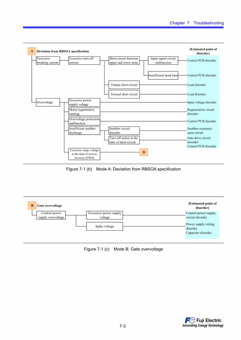
Chapter 7 Troubleshooting
7-3
Deviation from RBSOA specification [Estimated point ofdisorder]
Overvoltage
Ground short circuit
Short-circuit betweenupper and lower arms
Input signal circuitmalfunction
A
Control PCB disorderExcessivebreaking current
Excessive turn-offcurrent
Motor regenerativerunning
Insufficient dead time Control PCB disorder
Output short-circuit Load disorder
Load disorder
Excessive powersupply voltage Input voltage disorder
Regeneration circuitdisorder
Control PCB disorder
Snubber resistanceopen circuit
D
Overvoltage protectionmalfunctionInsufficient snubberdischarge
Snubber circuitdisorderTurn-off action at thetime of short-circuit
Gate drive circuitdisorderControl PCB disorder
Excessive surge voltageat the time of reverse
recovery (FWD)
Figure 7-1 (b) Mode A: Deviation from RBSOA specification
Gate overvoltage [Estimated point ofdisorder]
Capacitor disorder
B
Control powersupply overvoltage
Control power supplycircuit disorder
Power supply wiringdisorder
Excessive power supplyvoltage
Spike voltage
Figure 7-1 (c) Mode B: Gate overvoltage

Chapter 7 Troubleshooting
7-4
Excessive junction temperature rise (rapid temperature rise)
Gate drive circuit disorder
Excessive finwarpage
Input signalcircuit
malfunction
Insufficientelement
tightening force
Insufficientdead time
Insufficient dead time
Ground short circuit (repeatedshort-circuit current)
Increased carrier frequency
Input signalmalfunction(oscillation)
Short-circuit betweenupper and lower arms
Short-circuit betweenupper and lower arms
Insufficient compound weightadjustment
Dropped coolingcapacity
Cooling system disorder
Faulty anti-dust measures
Dropped or stopped coolingfan revolution
Clogged heat sink
Stack local overheating
Cooling fan disorder
Abnormal rise ofambient
temperature
Insufficient thermal compound weight
Input circuit disorder
Control PCB disorder
Control PCB disorder
Control PCB disorder
Load disorder
Control PCB disorder
Input circuit disorder
Over-load
Faulty fin warpage
Insufficient tightening torque
Control PCB disorder
Control PCB disorder
Excessive turn-on current
Increasedturn-on time
Insufficient controlpower supply voltage
Increased contactthermal resistance
Case temperaturerise
Insufficient control powersupply voltage
Insufficientdead time
Increasedturn-off loss
Increased switchingcount
Increasedturn-on loss
Excessive turn-off current
Input signal circuitmalfunction
Load disorder
Load disorder
Output short-circuit (repeatedshort-circuit current)
Control power supply circuitdisorder
Control PCB disorderShort-circuit of upper and
lower arms (repeated short-circuit current)
Snubber circuit disorder
Control PCB disorder
Excessive surgevoltage
C [Estimated point ofdisorder]
Increased steady-stateloss
Increased switchingloss
Increased saturatedvoltage VCE (sat)
Increased collectorcurrent
Over-current
Figure 7-1 (d) Mode C: Excessive junction temperature rise

Chapter 7 Troubleshooting
7-5
FWD breakdown
Overcurrent Charging circuit disorder
Overvoltage
Gate signal cracking causedby noise or similar
Control power supply circuitdisorder
Control PCB disorder
Snubber circuit disorder
Control power supply circuitdisorder
Excessive charge current at the time ofapplication to converter unit
Insufficient compound weightadjustment
Cooling fan disorderDropped or stopped cooling
fan revolution
Stack local overheating Cooling system disorder
Control PCB disorder
Faulty anti-dust measures
Increased contact thermalresistance
Case temperature rise
Insufficient elementtightening force
Excessive fin warpage
Insufficient thermalcompound weight
Clogged heat sink
Insufficient tightening torque
Faulty fin warpage
Control PCB disorder
Input signal circuit disorder
Control PCB disorder
Dropped power factor
[Estimated point ofdisorder]
Increased steady-stateloss
Load disorder
Excessive junctiontemperature rise Overload
D
Input signal malfunction
Increased switching loss Increasedswitching count
Increased carrier frequency
Dropped coolingcapacity
Increased control powersupply voltage
A
Abnormal rise ofambient
temperatureExcessive surge voltageat the time of reverse
recovery
Increased di/dt at the timeof turn-on
Minor pulse reverserecovery phenomenon
Excessive surge voltage atthe time of IGBT turn-off
Figure 7-1 (e) Mode D: FWD breakdown

Chapter 7 Troubleshooting
7-6
Control circuit breakdown
Power supply instabilityCapacitor disorder
Excessive staticelectricity
Insufficient static electricitymeasures
Spike voltage
Excessive power supply wiringlength
Excessive input unitvoltage
Control circuit disorder
Excessive minusvoltage
ON/OFF of control voltageimpression
External noise
External noise
Capacitor disorder
E [Estimated point ofdisorder]
Overvoltage Control power supply circuitdisorderExcessive control
power supply voltage
Figure 7-1 (f) Mode E: Control circuit breakdown

Chapter 7 Troubleshooting
7-7
Breakdown related to reliability and product handling
Long-term use in high temperature andhigh humidity conditions
Long-time voltage impression (high humidity impression(between C-E and between G-E)) in high temperatureconditions
Long-time voltage impression (high humidity and highhumidity impression (THB)) in high temperature and highhumidity conditions
Long-term use in hightemperature conditions
Thermal stress breakdown generated by rapid rise or fall of producttemperature (thermal impact)
Thermal stress fatigue breakdown to product internal wiring, etc. generated by changes insemiconductor chip temperature caused by rapid load change (∆Tc power cycle)
Storage in low temperature conditions(shelving under low temperature)
Storage in high temperature and highhumidity conditions (shelving underhigh temperature and high humidity)
Long-term storage in lowtemperature conditions
Long-term storage in high temperatureand high humidity conditions
Storage in high temperature conditions(shelving under high temperature)
Long-term storage in hightemperature conditions Conditions for storage
*For results ofreliability testsconducted by FujiElectric, see thespecification orreliability test report. Thermal stress fatigue generated by repeating of gradual up-down of
product temperature (temperature cycle, ∆Tc power cycle)Matching of appliedconditions with productservice life
Conditions for storage
Excessive contact resistance
Torque applied to terminalportion
Main terminal screwtightening
Conditions for assemblyduring product mounting
Inferior fixing of components atthe time of product mounting
Storage in condensableenvironment
Heat resistance ofsoldered terminals
Excessive heating duringterminal soldering
Storage in dusty environment
Conditions for transportation
Forceful dismounting
Impact Falling, impact, etc. duringtransportation Conditions for transportation
Product mounting conditions
Screw length
F [Estimated point ofdisorder]
Reliability (servicelife) breakdown
External force, load
Vibration
Excessive tighteningtorque
Torque applied to mountingportion
Loading conditions
Mounting work
Excessive vibration duringtransportation (products, devices)
Breakdown caused byerroneous handling
Long-term use in atmosphere ofhydrogen sulfide or similarUse in corrosive gas atmosphere
Excessive loading during product storage
Excessive stress applied to terminals andcase at the time of IPM mounting
Excessive stress applied to terminals andcase at the time of IPM dismounting
Excessive screw length used for mainterminals
Insufficient mainterminal tighteningtorque
Storage in inferiorenvironment
Storage in corrosive gasatmosphere
Figure 7-1 (g) Mode F: Breakdown related to reliability and product handling

Chapter 7 Troubleshooting
7-8
3 Alarm factor analysis tree chart
When the system equipped with the IPM has stopped and an alarm signal is generated, first carry out
investigations to identify where the alarm signal was generated from. Possible locations are athe IPM or the
device control circuit.
If the alarm was sent from the IPM, then identify the factor in accordance with the factor tree chart
indicated below. V-IPM is easy to identify which protective function is activated by checking the alarm pulse
width. Therefore, you can shorten the factor analysis time.
In addition, the alarm output voltage can be easily measured by connecting a 1.3 KΩ resistor in series
between the IPM alarm terminal and the cathode terminal of the alarming photodiode.
Occurrence of an IPM alarm
OvercurrenttALM Typ = 2 ms
tALM Typ = 4 ms
tALM Typ = 8 ms
[Method for identification of alarm factor]• A short-pulse alarm of an μs is produced. ⇒See chapter 6 section 1.2.1• Observe the Vcc waveform using an oscilloscope while the motor is running. It is desirable that the point of observation is located nearest to an IPM control terminal.• Confirm that Vcc < 20 V, dv/dt ≤ 5 V/μs, ripple voltage ≤ ±10% (with every one of fourpower supply unit).• Confirm that no external wiring connection is made between IPM control GND and main terminal GND. If wiring is made, noise current flows through IPM control circuit.• If the drive IC was broken, there is a large possibility where the value Icc rises to an abnormal level. Example: It is abnormal, if Iccp ≥ 10 mA, Iccn ≥ 20 mA, and @Vin = OFF.
[Method for identification of alarm factor]• Measure control power supply voltage Vcc, DC input voltage Vdc and output current Io.• Measure case temperature Tc just below the chip, calculate ∆Tj-c and estimate the value of Tj.• Check the IPM mounting method. (Fin flatness, thermal compound, etc.)
Erroneous alarmUnstable tALM
If control power supply voltage Vcc exceeds absolute maximum rating, which is 20 V, or ifexcessive dv/dt or ripple was impressed, there is a possibility where the drive IC is brokenand an erroneous alarm is output.Furthermore, also in case noise current flows to the IPM control circuit, there is a possibilitywhere the IC voltage becomes unstable and an erroneous alarm is output.
The chip temperature is detected by the temperature detection element (diode) that is builtin every IGBT chip.The IGBT is OFF for protection, if the TjOH trip level was exceeded continuously for 1 ms.
Alarm factor and method for identificationPhenomenon
Normalalarm
The collector current is detected by checking the current that flows to the current senseIGBT that is built in every IGBT chip.The IGBT is OFF for protection, if the overcurrent trip level was continuously exceeded forabout 5 μs.
[Method for identification of alarm factor]• Observe the alarm and output current (U, V, W) using an oscilloscope.• Observe the alarm and DC input current (P, N) using an oscilloscope.• Observe the change in the current 5μs before occurrence of alarm output.• Where a CT or similar is used for current detection, check the trip level and point ofdetection.
Low control powersupply voltage
Chip overheat
The IGBT is OFF for protection, if control power supply voltage Vcc was of undervoltage triplevel or less continuously for 20 μs.
[Method for identification of alarm factor]• Observe the alarm and Vcc using an oscilloscope.• Observe the change in the current 20 μs before occurrence of alarm output.

1. This Catalog contains the product specifications, characteristics, data, materials, and structures as of July 2015. The contents are subject to change without notice for specification changes or other reasons. When using a product listed in this Catalog, be sur to obtain the latest specifications.
2. All applications described in this Catalog exemplify the use of Fuji's products for your reference only. No right or license, either express or
implied, under any patent, copyright, trade secret or other intellectual property right owned by Fuji Electric Co., Ltd. is (or shall be deemed) granted. Fuji Electric Co., Ltd. makes no representation or warranty, whether express or implied, relating to the infringement or alleged infringement of other's intellectual property rights which may arise from the use of the applications described herein.
3. Although Fuji Electric Co., Ltd. is enhancing product quality and reliability, a small percentage of semiconductor products may become faulty.
When using Fuji Electric semiconductor products in your equipment, you are requested to take adequate safety measures to prevent the equipment from causing a physical injury, fire, or other problem if any of the products become faulty. It is recommended to make your design fail-safe, flame retardant, and free of malfunction.
4. The products introduced in this Catalog are intended for use in the following electronic and electrical equipment which has normal reliability
requirements. • Computers • OA equipment • Communications equipment (terminal devices) • Measurement equipment • Machine tools • Audiovisual equipment • Electrical home appliances • Personal equipment • Industrial robots etc.
5. If you need to use a product in this Catalog for equipment requiring higher reliability than normal, such as for the equipment listed below, it
is imperative to contact Fuji Electric Co., Ltd. to obtain prior approval. When using these products for such equipment, take adequate measures such as a backup system to prevent the equipment from malfunctioning even if a Fuji's product incorporated in the equipment becomes faulty. • Transportation equipment (mounted on cars and ships) • Trunk communications equipment • Traffic-signal control equipment • Gas leakage detectors with an auto-shut-off feature • Emergency equipment for responding to disasters and anti-burglary devices • Safety devices • Medical equipment
6. Do not use products in this Catalog for the equipment requiring strict reliability such as the following and equivalents to strategic equipment
(without limitation). • Space equipment • Aeronautic equipment • Nuclear control equipment • Submarine repeater equipment
7. Copyright ©1996-2014 by Fuji Electric Co., Ltd. All rights reserved.
No part of this Catalog may be reproduced in any form or by any means without the express permission of Fuji Electric Co., Ltd.
8. If you have any question about any portion in this Catalog, ask Fuji Electric Co., Ltd. or its sales agents before using the product. Neither Fuji Electric Co., Ltd. nor its agents shall be liable for any injury caused by any use of the products not in accordance with instructions set forth herein.