fsdm0265rnb - farnell element14 · • frequency modulation for emi reduction ... facsimile &...
TRANSCRIPT
©2005 Fairchild Semiconductor Corporation
www.fairchildsemi.com
Rev.1.0.4FPSTM is a trademark of Fairchild Semiconductor Corporation.
Features• Internal Avalanche Rugged Sense FET• Consumes only 0.65W at 240VAC & 0.3W load with
Advanced Burst-Mode Operation• Frequency Modulation for EMI Reduction• Precision Fixed Operating Frequency• Internal Start-up Circuit• Pulse-by-Pulse Current Limiting• Over Voltage Protection (OVP)• Over Load Protection (OLP)• Internal Thermal Shutdown Function (TSD)• Auto-Restart Mode• Under Voltage Lockout (UVLO)• Low Operating Current (3mA)• Adjustable Peak Current Limit• Built-in Soft Start
Applications• SMPS for VCR, SVR, STB, DVD & DVCD Player• SMPS for Printer, Facsimile & Scanner• Adapter for Camcorder
Related Application Notes• AN-4137, 4141, 4147(Flyback) / AN-4134(Forward)
DescriptionThe FSDM0265RNB consists of an integrated Pulse WidthModulator (PWM) and Sense FET, and is specificallydesigned for high performance off-line Switch Mode PowerSupplies (SMPS) with minimal external components. Thisdevices is an integrated high voltage power switching regu-lator which combines an avalanche rugged Sense FET with acurrent mode PWM control block. The integrated PWM con-troller features include: a fixed oscillator with frequencymodulation for reduced EMI, Under Voltage Lock Out(UVLO) protection, Leading Edge Blanking (LEB), an opti-mized gate turn-on/turn-off driver, Thermal Shut Down(TSD) protection and temperature compensated precisioncurrent sources for loop compensation and fault protectioncircuitry. The FSDM0265RNB offers better performance inSoft Start than FSDM0265RN. When compared to a discreteMOSFET and controller or RCC switching converter solu-tion, the FSDM0265RNB reduces total component count,design size, weight while increasing efficiency, productivityand system reliability. This device provides a basic platformthat is well suited for the design of cost-effective flybackconverters.
Notes: 1. Typical continuous power in a non-ventilated enclosed
adapter with sufficient drain pattern as a heat sinker, at50°C ambient.
2. Maximum practical continuous power in an open framedesign with sufficient drain pattern as a heat sinker, at 50°Cambient.
3. 230 VAC or 100/115 VAC with doubler.
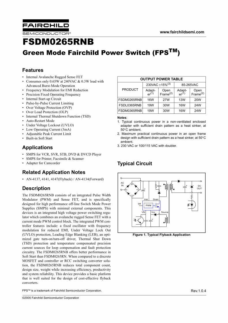
Typical Circuit
Figure 1. Typical Flyback Application
OUTPUT POWER TABLE
PRODUCT230VAC ±15%(3) 85-265VAC
Adapt-er(1)
Open Frame(2)
Adapt-er(1)
Open Frame(2)
FSDM0265RNB 16W 27W 13W 20W
FSDL0365RNB 19W 30W 16W 24W
FSDM0365RNB 19W 30W 16W 24W
Drain
Source
Vstr
Vfb Vcc
PWM
ACIN DC
OUT
Ipk
FSDM0265RNBGreen Mode Fairchild Power Switch (FPSTM)

FSDM0265RNB
2
Internal Block Diagram
Figure 2. Functional Block Diagram of FSDM0265RNB
8V/12V
2 6,7,8
1
3
Vref InternalBias
S
Q
Q
R
OSCVcc Vcc
IDELAY IFB
VSD
TSD
Vovp
Vcc
Soft Start
S
Q
Q
R
R2.5R
Vcc good
Vcc Drain
Vfb
GND
Gatedriver
5Vstr
ICH
Vcc good
VBURL/VBURH
LEB
+
-
4Ipk
Freq.Modulation
VBURH
Vcc
IBUR(pk)
Burst
Normal PWM
FSDM0265RNB
3
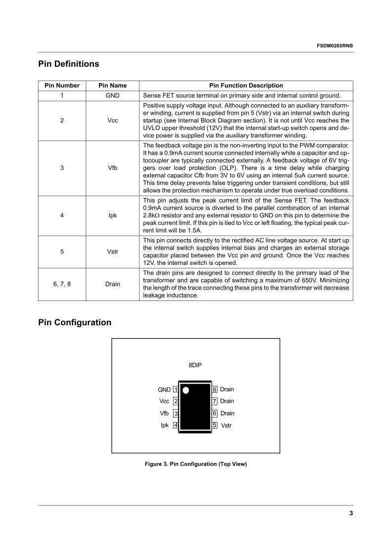
Pin Definitions
Pin Configuration
Figure 3. Pin Configuration (Top View)
Pin Number Pin Name Pin Function Description1 GND Sense FET source terminal on primary side and internal control ground.
2 Vcc
Positive supply voltage input. Although connected to an auxiliary transform-er winding, current is supplied from pin 5 (Vstr) via an internal switch duringstartup (see Internal Block Diagram section). It is not until Vcc reaches theUVLO upper threshold (12V) that the internal start-up switch opens and de-vice power is supplied via the auxiliary transformer winding.
3 Vfb
The feedback voltage pin is the non-inverting input to the PWM comparator.It has a 0.9mA current source connected internally while a capacitor and op-tocoupler are typically connected externally. A feedback voltage of 6V trig-gers over load protection (OLP). There is a time delay while chargingexternal capacitor Cfb from 3V to 6V using an internal 5uA current source.This time delay prevents false triggering under transient conditions, but stillallows the protection mechanism to operate under true overload conditions.
4 Ipk
This pin adjusts the peak current limit of the Sense FET. The feedback0.9mA current source is diverted to the parallel combination of an internal2.8kΩ resistor and any external resistor to GND on this pin to determine thepeak current limit. If this pin is tied to Vcc or left floating, the typical peak cur-rent limit will be 1.5A.
5 Vstr
This pin connects directly to the rectified AC line voltage source. At start upthe internal switch supplies internal bias and charges an external storagecapacitor placed between the Vcc pin and ground. Once the Vcc reaches12V, the internal switch is opened.
6, 7, 8 Drain
The drain pins are designed to connect directly to the primary lead of thetransformer and are capable of switching a maximum of 650V. Minimizingthe length of the trace connecting these pins to the transformer will decreaseleakage inductance.
1
2
3
4 5
6
7
8GND
Vcc
Vfb
Ipk Vstr
Drain
Drain
Drain
8DIP

FSDM0265RNB
4
Absolute Maximum Ratings(Ta=25°C, unless otherwise specified)
Note:1. Repetitive rating: Pulse width is limited by maximum junction temperature2. L = 51mH, starting Tj = 25°C
Thermal Impedance(Ta=25°C, unless otherwise specified)
Note:1. Free standing with no heatsink; Without copper clad.
/ Measurement Condition : Just before junction temperature TJ enters into OTP.2. Measured on the DRAIN pin close to plastic interface.3. Measured on the PKG top surface.
- all items are tested with the standards JESD 51-2 and 51-10 (DIP).
Characteristic Symbol Value UnitDrain Pin Voltage VDRAIN 650 VVstr Pin Voltage VSTR 650 VDrain Current Pulsed(1) IDM 8.0 ASingle Pulsed Avalanche Energy(2) EAS 68 mJSupply Voltage VCC 20 VFeedback Voltage Range VFB -0.3 to VCC VTotal Power Dissipation PD 1.56 WOperating Junction Temperature TJ Internally limited °COperating Ambient Temperature TA -25 to +85 °CStorage Temperature TSTG -55 to +150 °C
Parameter Symbol Value Unit8DIPJunction-to-Ambient Thermal(1) θJA 79.64 °C/WJunction-to-Case Thermal(2) θJC 18.20 °C/WJunction-to-Top Thermal(3) ψJT 34.30 °C/W

FSDM0265RNB
5
Electrical Characteristics (Ta = 25°C unless otherwise specified)
Note:1. Pulse test: Pulse width ≤ 300us, duty ≤ 2% 2. These parameters, although guaranteed, are tested in EDS (wafer test) process3. These parameters, although guaranteed, are not 100% tested in production
Parameter Symbol Condition Min. Typ. Max. UnitSENSE FET SECTION
Zero-Gate-Voltage Drain Current IDSS VDS=650V, VGS=0V - - 50 µA VDS=520V, VGS=0V, TC=125°C - - 200 µA
Drain-Source On-State Resistance(1) RDS(ON) VGS=10V, ID=0.5A - 5.0 6.0 Ω
Input Capacitance CISSVGS=0V, VDS=25V,f=1MHz
- 550 - pFOutput Capacitance COSS - 38 - pFReverse Transfer Capacitance CRSS - 17 - pFTurn-On Delay Time td(on)
VDS=325V, ID=1.0A
- 20 - nsRise Time tr - 15 - nsTurn-Off Delay Time td(off) - 55 - nsFall Time tf - 25 - nsCONTROL SECTION Switching Frequency fOSC 61 67 73 KHzSwitching Frequency Modulation ∆fMOD ±1.5 ±2.0 ±2.5 KHzSwitching Frequency Variation(2) ∆fOSC -25°C ≤ Ta ≤ 85°C - ±5 ±10 % Maximum Duty Cycle DMAX 62 67 72 % Minimum Duty Cycle DMIN 0 0 0 %
UVLO Threshold VoltageVSTART VFB=GND 11 12 13 V VSTOP VFB=GND 7 8 9 V
Feedback Source Current IFB VFB=GND 0.7 0.9 1.1 mA Internal Soft Start Time tS/S VFB=4V 10 15 20 ms BURST MODE SECTION
Burst Mode VoltageVBURH - 0.4 0.5 0.6 V VBURL - 0.25 0.35 0.45 V
PROTECTION SECTION Peak Current Limit ILIM Max. inductor current 1.3 1.5 1.7 A Current Limit Delay Time(3) tCLD - 500 - ns Thermal Shutdown Temperature TSD - 125 140 - °CShutdown Feedback Voltage VSD 5.5 6.0 6.5 V Over Voltage Protection VOVP 18 19 - VShutdown Delay Current IDELAY VFB=4V 3.5 5.0 6.5 µA Leading Edge Blanking Time tLEB 200 - - ns TOTAL DEVICE SECTION Operating Supply Current (control part only) IOP VCC=14V 1 3 5 mA Start-Up Charging Current ICH VCC=0V 0.7 0.85 1.0 mA Vstr Supply Voltage VSTR VCC=0V 35 - - V

FSDM0265RNB
6
Comparison Between KA5x0265RN and FSDM0265RNB
Function KA5x0265RN FSDM0265RNB FSDM0265RNB AdvantagesSoft-Start not applicable 15ms • Gradually increasing current limit
during soft-start further reduces peak current and voltage stresses
• Eliminates external components used for soft-start in most applications
• Reduces or eliminates output overshoot
External Current Limit not applicable Programmable of default current limit
• Smaller transformer• Allows power limiting (constant over-
load power)• Allows use of larger device for lower
losses and higher efficiency.Frequency Modulation not applicable ±2.0KHz @67KHz • Reduces conducted EMIBurst Mode Operation not applicable Built into controller • Improves light load efficiency
• Reduces power consumption at no-load
• Transformer audible noise reductionDrain Creepage at Package
1.02mm 7.62mm • Greater immunity to arcing provoked by dust, debris and other contami-nants

FSDM0265RNB
7
Typical Performance Characteristics (Control Part)(These characteristic graphs are normalized at Ta = 25°C)
0.00
0.200.40
0.600.80
1.001.20
-50 0 50 100 150
Temp[]
Nor
mal
ized
Operating Frequency (Fosc) vs. Ta
0.000.200.400.600.801.001.20
-50 0 50 100 150
Temp[]
Nor
mal
ized
Frequency Modulation (∆FMOD) vs. Ta
0.00
0.20
0.40
0.60
0.80
1.00
1.20
-50 0 50 100 150
Temp[]
Nor
mal
ized
Maximum Duty Cycle (DMAX) vs. Ta
0.00
0.20
0.40
0.60
0.80
1.00
1.20
-50 0 50 100 150
T emp[]
Nor
mal
ized
Operating Supply Current (IOP) vs. Ta
0.00
0.20
0.40
0.60
0.80
1.00
1.20
-50 0 50 100 150
Temp[]
Nor
mal
ized
Start Threshold Voltage (VSTART) vs. Ta
0.00
0.20
0.40
0.60
0.80
1.00
1.20
-50 0 50 100 150
Temp[]
Nor
mal
ized
Stop Threshold Voltage (VSTOP) vs. Ta

FSDM0265RNB
8
Typical Performance Characteristics (Continued)
0.00
0.20
0.40
0.60
0.80
1.00
1.20
-50 0 50 100 150
Temp[]
Nor
mal
ized
Feedback Source Current (IFB) vs. Ta
0.00
0.20
0.40
0.60
0.80
1.00
1.20
-50 0 50 100 150
Temp[]
Nor
mal
ized
Peak Current Limit (ILIM) vs. Ta
0.00
0.20
0.40
0.60
0.80
1.00
1.20
-50 0 50 100 150
Temp[]
Nor
mal
ized
Start Up Charging Current (ICH) vs. Ta
0.00
0.20
0.40
0.60
0.80
1.00
1.20
-50 0 50 100 150
Temp[]
Nor
mal
ized
Burst Peak Current (IBUR(pk)) vs. Ta
0.00
0.20
0.40
0.60
0.80
1.00
1.20
-50 0 50 100 150
Temp[]
Nor
mal
ized
Over Voltage Protection (VOVP) vs. Ta
FSDM0265RNB
9
Functional Description
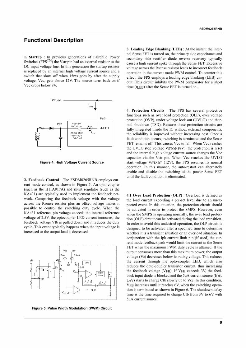
1. Startup : In previous generations of Fairchild PowerSwitches (FPSTM) the Vstr pin had an external resistor to theDC input voltage line. In this generation the startup resistoris replaced by an internal high voltage current source and aswitch that shuts off when 15ms goes by after the supplyvoltage, Vcc, gets above 12V. The source turns back on ifVcc drops below 8V.
Figure 4. High Voltage Current Source
2. Feedback Control : The FSDM0265RNB employs cur-rent mode control, as shown in Figure 5. An opto-coupler(such as the H11A817A) and shunt regulator (such as theKA431) are typically used to implement the feedback net-work. Comparing the feedback voltage with the voltageacross the Rsense resistor plus an offset voltage makes itpossible to control the switching duty cycle. When theKA431 reference pin voltage exceeds the internal referencevoltage of 2.5V, the optocoupler LED current increases, thefeedback voltage Vfb is pulled down and it reduces the dutycycle. This event typically happens when the input voltage isincreased or the output load is decreased.
Figure 5. Pulse Width Modulation (PWM) Circuit
3. Leading Edge Blanking (LEB) : At the instant the inter-nal Sense FET is turned on, the primary side capacitance andsecondary side rectifier diode reverse recovery typicallycause a high current spike through the Sense FET. Excessivevoltage across the Rsense resistor leads to incorrect feedbackoperation in the current mode PWM control. To counter thiseffect, the FPS employs a leading edge blanking (LEB) cir-cuit. This circuit inhibits the PWM comparator for a shorttime (tLEB) after the Sense FET is turned on.
4. Protection Circuits : The FPS has several protectivefunctions such as over load protection (OLP), over voltageprotection (OVP), under voltage lock out (UVLO) and ther-mal shutdown (TSD). Because these protection circuits arefully integrated inside the IC without external components,the reliability is improved without increasing cost. Once afault condition occurs, switching is terminated and the SenseFET remains off. This causes Vcc to fall. When Vcc reachesthe UVLO stop voltage VSTOP (8V), the protection is resetand the internal high voltage current source charges the Vcccapacitor via the Vstr pin. When Vcc reaches the UVLOstart voltage VSTART (12V), the FPS resumes its normaloperation. In this manner, the auto-restart can alternatelyenable and disable the switching of the power Sense FETuntil the fault condition is eliminated.
4.1 Over Load Protection (OLP) : Overload is defined asthe load current exceeding a pre-set level due to an unex-pected event. In this situation, the protection circuit shouldbe activated in order to protect the SMPS. However, evenwhen the SMPS is operating normally, the over load protec-tion (OLP) circuit can be activated during the load transition.In order to avoid this undesired operation, the OLP circuit isdesigned to be activated after a specified time to determinewhether it is a transient situation or an overload situation. Inconjunction with the Ipk current limit pin (if used) the cur-rent mode feedback path would limit the current in the SenseFET when the maximum PWM duty cycle is attained. If theoutput consumes more than this maximum power, the outputvoltage (Vo) decreases below its rating voltage. This reducesthe current through the opto-coupler LED, which alsoreduces the opto-coupler transistor current, thus increasingthe feedback voltage (VFB). If VFB exceeds 3V, the feed-back input diode is blocked and the 5uA current source (IDE-LAY) starts to charge Cfb slowly up to Vcc. In this condition,VFB increases until it reaches 6V, when the switching opera-tion is terminated as shown in Figure 6. The shutdown delaytime is the time required to charge Cfb from 3V to 6V with5uA current source.
Vin,dc
Vstr
Vcc
15ms afterVcc≥12VUVLO off
Vcc<8VUVLO on
ISTR
J-FETICH
3 OSC
Vcc Vcc
5uA 0.9mA
VSD
R
2.5R
Gatedriver
OLP
D1 D2
VFB
Vfb
431
CFB
Vo
+
-
VFB,in

FSDM0265RNB
10
Figure 6. Over Load Protection (OLP)
4.2 Thermal Shutdown (TSD) : The Sense FET and thecontrol IC are integrated, making it easier for the control ICto detect the temperature of the Sense FET. When the tem-perature exceeds approximately 140°C, thermal shutdown isactivated.
4.3 Over Voltage Protection (OVP) : In the event of a mal-function in the secondary side feedback circuit, or an openfeedback loop caused by a soldering defect, the currentthrough the opto-coupler transistor becomes almost zero(refer to Figure 5). Then, VFB climbs up in a similar mannerto the over load situation, forcing the preset maximum cur-rent to be supplied to the SMPS until the over load protectionis activated. Because excess energy is provided to the output,the output voltage may exceed the rated voltage before theover load protection is activated, resulting in the breakdownof the devices in the secondary side. In order to prevent thissituation, an over voltage protection (OVP) circuit isemployed. In general, Vcc is proportional to the output volt-age and the FPS uses Vcc instead of directly monitoring theoutput voltage. If VCC exceeds 19V, OVP circuit is activatedresulting in termination of the switching operation. In orderto avoid undesired activation of OVP during normal opera-tion, Vcc should be properly designed to be below 19V.
5. Soft Start : The FPS has an internal soft start circuit thatslowly increases the feedback voltage together with theSense FET current after it starts up. The typical soft starttime is 15msec, as shown in Figure 7, where progressiveincrements of the Sense FET current are allowed during thestart-up phase. The pulse width to the power switchingdevice is progressively increased to establish the correctworking conditions for transformers, inductors, and capaci-tors. The voltage on the output capacitors is progressivelyincreased with the intention of smoothly establishing therequired output voltage. It also helps to prevent transformersaturation and reduce the stress on the secondary diode.
Figure 7. Soft Start Function
6. Burst Operation : In order to minimize power dissipationin standby mode, the FPS enters burst mode operation. Asthe load decreases, the feedback voltage decreases. Asshown in Figure 8, the device automatically enters burstmode when the feedback voltage drops belowVBURH(500mV). Switching still continues but the currentlimit is set to a fixed limit internally to minimize flux densityin the transformer. The fixed current limit is larger than thatdefined by VFB = VBURH and therefore, VFB is drivendown further. Switching continues until the feedback voltagedrops below VBURL(350mV). At this point switching stopsand the output voltages start to drop at a rate dependent onthe standby current load. This causes the feedback voltage torise. Once it passes VBURH, switching resumes. The feed-back voltage then falls and the process repeats. Burst modeoperation alternately enables and disables switching of theSense FET and reduces switching loss in Standby mode.
VFB
t
3V
6V
Over Load Protection
t12= CFB×(V(t2)-V(t1)) / IDELAY
t1 t2
VtVVtVAII
tVtVCt DELAYDELAY
FB 6)(,3)(,5;)()(21
1212 ===
−= µ
1ms15steps
Current limit0.3A
1.5A
t
Drain current
DRAIN
GND
Rsense
#6,7,8
#1
ILIM
5V

FSDM0265RNB
11
Figure 8. Burst Operation Function
7. Frequency Modulation : Modulating the switching fre-quency of a switched power supply can reduce EMI. Fre-quency modulation can reduce EMI by spreading the energyover a wider frequency range than the bandwidth measuredby the EMI test equipment. The amount of EMI reduction isdirectly related to the depth of the reference frequency. Ascan be seen in Figure 9, the frequency changes from 65KHzto 69KHz in 4ms for the FSDM0265RNB. Frequency modu-lation allows the use of a cost effective inductor instead of anAC input mode choke to satisfy the requirements of worldwide EMI limits.
Figure 9. Frequency Modulation Waveform
Figure 10. KA5-series FPS Full Range EMI scan(67KHz, no Frequency Modulation) with DVD Player SET
Figure 11. FSDX-series FPS Full Range EMI Scan (67KHz, with Frequency Modulation) with DVD Player SET
VBURH
SwitchingOFF
CurrentWaveform
BurstOperation
NormalOperation
VFB
VBURL
SwitchingOFF
BurstOperation
3
Vcc Vcc
IDELAY
IFB
R2.5R
Vfb
VBURL/VBURH
PWM
+
-VBURH
Vcc
IBUR(pk)
Burst
Normal
MOSFETCurrent
tsfs=1/ts
67kHz69kHz
65kHz
4ms t
DrainCurrent
Frequency (MHz)
Am
plitu
de (d
BµV
)
Frequency (MHz)
Am
plitu
de (d
BµV
)

FSDM0265RNB
12
8. Adjusting Peak Current Limit : As shown in Figure 12,a combined 2.8kΩ internal resistance is connected to thenon-inverting lead on the PWM comparator. A externalresistance of Rx on the current limit pin forms a parallelresistance with the 2.8kΩ when the internal diodes arebiased by the main current source of 900uA.
Figure 12. Peak Current Limit Adjustment
For example, FSDM0265RNB has a typical Sense FET peakcurrent limit (ILIM) of 1.5A. ILIM can be adjusted to 1A byinserting Rx between the Ipk pin and the ground. The valueof the Rx can be estimated by the following equations:
1.5A : 1A = 2.8kΩ : XkΩ ,
X = Rx || 2.8kΩ .
(X represents the resistance of the parallel network)
3
Vcc Vcc
IDELAY IFB 2kΩVfbPWM
Comparator
4Ipk
0.8kΩ
Rx
SenseFETCurrentSense
900uA5uA

FSDM0265RNB
13
Application Tips
1. Methods of Reducing Audible Noise
Switching mode power converters have electronic andmagnetic components, which generate audible noises whenthe operating frequency is in the range of 20~20,000 Hz.Even though they operate above 20 kHz, they can makenoise depending on the load condition. Designers canemploy several methods to reduce these noises. Here arethree of these methods:
Glue or Varnish
The most common method involves using glue or varnishto tighten magnetic components. The motion of core, bobbinand coil and the chattering or magnetostriction of core cancause the transformer to produce audible noise. The use ofrigid glue and varnish helps reduce the transformer noise.But, it also can crack the core. This is because suddenchanges in the ambient temperature cause the core and theglue to expand or shrink in a different ratio according to thetemperature.
Ceramic Capacitor
Using a film capacitor instead of a ceramic capacitor as asnubber capacitor is another noise reduction solution. Somedielectric materials show a piezoelectric effect depending onthe electric field intensity. Hence, a snubber capacitorbecomes one of the most significant sources of audiblenoise. It is considerable to use a zener clamp circuit insteadof an RCD snubber for higher efficiency as well as loweraudible noise.
Adjusting Sound Frequency
Moving the fundamental frequency of noise out of 2~4 kHzrange is the third method. Generally, humans are more sensi-tive to noise in the range of 2~4 kHz. When the fundamentalfrequency of noise is located in this range, one perceives thenoise as louder although the noise intensity level is identical.Refer to Figure 13. Equal Loudness Curves.
When FPS acts in Burst mode and the Burst operation issuspected to be a source of noise, this method may be help-ful. If the frequency of Burst mode operation lies in therange of 2~4 kHz, adjusting feedback loop can shift theBurst operation frequency. In order to reduce the Burst oper-ation frequency, increase a feedback gain capacitor (CF),opto-coupler supply resistor (RD) and feedback capacitor(CB) and decrease a feedback gain resistor (RF) as shown inFigure 14. Typical Feedback Network of FPS.
Figure 13. Equal Loudness Curves
Figure 14. Typical Feedback Network of FPS
2. Other Reference Materials
AN-4134: Design Guidelines for Off-line Forward Convert-ers Using Fairchild Power Switch (FPSTM)
AN-4137: Design Guidelines for Off-line Flyback Convert-ers Using Fairchild Power Switch (FPS)
AN-4140: Transformer Design Consideration for Off-lineFlyback Converters using Fairchild Power Switch(FPSTM)
AN-4141: Troubleshooting and Design Tips for FairchildPower Switch (FPSTM) Flyback Applications
AN-4147: Design Guidelines for RCD Snubber of Flyback
AN-4148: Audible Noise Reduction Techniques for FPSApplications
FSDM0265RNB
14
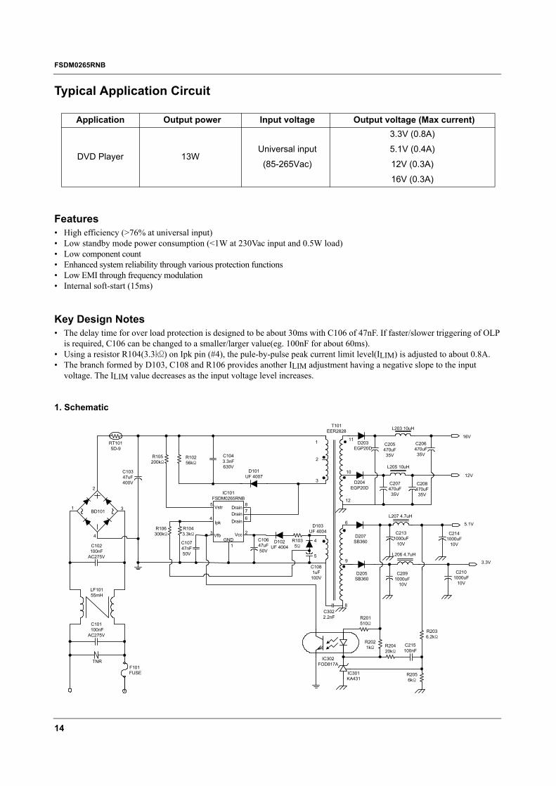
Typical Application Circuit
Features• High efficiency (>76% at universal input)• Low standby mode power consumption (<1W at 230Vac input and 0.5W load)• Low component count • Enhanced system reliability through various protection functions • Low EMI through frequency modulation• Internal soft-start (15ms)
Key Design Notes• The delay time for over load protection is designed to be about 30ms with C106 of 47nF. If faster/slower triggering of OLP
is required, C106 can be changed to a smaller/larger value(eg. 100nF for about 60ms).• Using a resistor R104(3.3) on Ipk pin (#4), the pule-by-pulse peak current limit level(ILIM) is adjusted to about 0.8A.• The branch formed by D103, C108 and R106 provides another ILIM adjustment having a negative slope to the input
voltage. The ILIM value decreases as the input voltage level increases.
1. Schematic
Application Output power Input voltage Output voltage (Max current)
DVD Player 13WUniversal input
(85-265Vac)
3.3V (0.8A)
5.1V (0.4A)
12V (0.3A)
16V (0.3A)
3
4
C102100nF
AC275V
LF10155mH
C101 100nF
AC275V
F101 FUSE
C10347uF400V
R10256kΩ
C1043.3nF630V
D101UF 4007
IC101FSDM0265RNB
C10747nF50V
C10647uF50V
D102UF 4004
R1035Ω
1
2
3
4
5
8
9
6
12
10
11
T101EER2828
D203EGP20D
C205470uF35V
C206470uF35V
L203 10uH
L207 4.7uH
L206 4.7uH
D204EGP20D
C207470uF35V
C208470uF35V
C2141000uF
10V
C2131000uF
10V
D207SB360
D205SB360
C2091000uF
10V
C2101000uF
10V
R201510Ω
R2021kΩ
R2036.2kΩ
R20420kΩ
C215100nF
R2056kΩ
IC302FOD817A
BD101
L205 10uH
Vstr
Ipk
Vfb Vcc
Drain
GND
6
1
23
4
51
2
DrainDrain
78
IC301KA431
16V
R1043.3kΩ
TNR
R105200kΩ
R106300kΩ
D103UF 4004
C1081uF
100V
C3022.2nF
12V
5.1V
3.3V
RT1015D-9

FSDM0265RNB
15
2. Transformer Schematic Diagram
3. Winding Specification
4. Electrical Characteristics
5. Core & BobbinCore : EER2828 ( Ae = 86.66 mm2 )Bobbin : EER2828
EER2828
N12V
1
6
7
8
9
10
11
12
N16V
N5.1V
N3.3V
Np/2
Na
2
3
4
5
Np/2
6mm 3mm
N16V
N12V
Na
N5.1V
N3.3V
Np/2
Np/2
P in (S → F ) W ire Turns W ind ing M ethod
N p/2 3 → 2 0.25φ ×1 50 C enter Solenoid w ind ing
Insu la tion : Polyester Tape t = 0 .050m m , 2Layers
N 3.3V 9 → 8 0.33φ ×2 4 C enter Solenoid w ind ing
Insu la tion : Polyester Tape t = 0 .050m m , 2Layers
N 5.1V 6 → 9 0.33φ ×1 2 C enter Solenoid w ind ing
Insu la tion : Polyester Tape t = 0 .050m m , 2Layers
N a 4 → 5 0.25φ ×1 16 C enter Solenoid w ind ing
Insu la tion : Polyester Tape t = 0 .050m m , 2Layers
N 12V 10 → 12 0.33φ ×1 14 C enter Solenoid w ind ing
Insu la tion : Polyester Tape t = 0 .050m m , 3Layers
N 16V 11 → 12 0.33φ ×1 18 C enter Solenoid w ind ing
Insu la tion : Polyester Tape t = 0 .050m m , 2Layers
N p/2 2→ 1 0.25φ ×1 50 C enter Solenoid w ind ing
Insu la tion : Polyester Tape t = 0 .050m m , 2Layers
P in S p e c . R e m a rk
In d u c ta n c e 1 - 3 1 .4 m H ± 1 0 % 1 0 0 k H z , 1 V
L e a k a g e 1 - 3 2 5 u H M a x . S h o r t a ll o th e r p in s
FSDM0265RNB
16
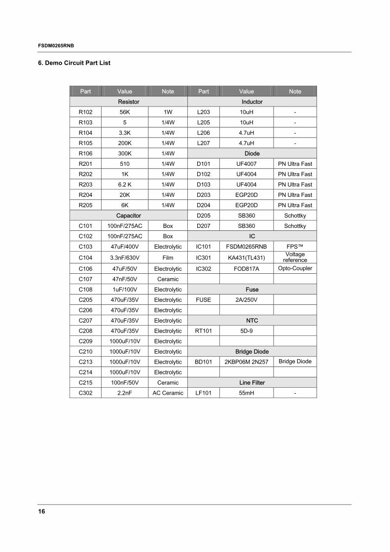
6. Demo Circuit Part List
Part Value Note Part Value Note
Resistor Inductor
R102 56K 1W L203 10uH -
R103 5 1/4W L205 10uH -
R104 3.3K 1/4W L206 4.7uH -
R105 200K 1/4W L207 4.7uH -
R106 300K 1/4W Diode
R201 510 1/4W D101 UF4007 PN Ultra Fast
R202 1K 1/4W D102 UF4004 PN Ultra Fast
R203 6.2 K 1/4W D103 UF4004 PN Ultra Fast
R204 20K 1/4W D203 EGP20D PN Ultra Fast
R205 6K 1/4W D204 EGP20D PN Ultra Fast
Capacitor D205 SB360 Schottky
C101 100nF/275AC Box D207 SB360 Schottky
C102 100nF/275AC Box IC
C103 47uF/400V Electrolytic IC101 FSDM0265RNB FPS™
C104 3.3nF/630V Film IC301 KA431(TL431) Voltage reference
C106 47uF/50V Electrolytic IC302 FOD817A Opto-Coupler
C107 47nF/50V Ceramic
C108 1uF/100V Electrolytic Fuse
C205 470uF/35V Electrolytic FUSE 2A/250V
C206 470uF/35V Electrolytic
C207 470uF/35V Electrolytic NTC
C208 470uF/35V Electrolytic RT101 5D-9
C209 1000uF/10V Electrolytic
C210 1000uF/10V Electrolytic Bridge Diode
C213 1000uF/10V Electrolytic BD101 2KBP06M 2N257 Bridge Diode
C214 1000uF/10V Electrolytic
C215 100nF/50V Ceramic Line Filter
C302 2.2nF AC Ceramic LF101 55mH -
FSDM0265RNB
17
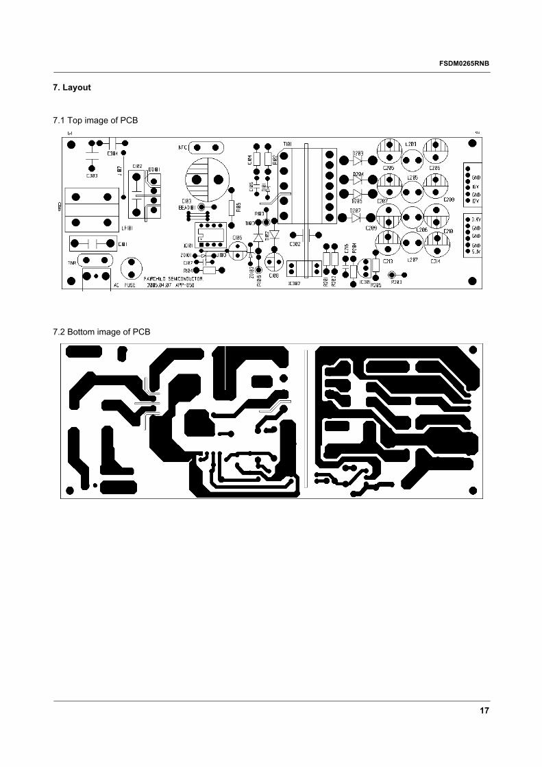
7. Layout
7.1 Top image of PCB
7.2 Bottom image of PCB
FSDM0265RNB
18
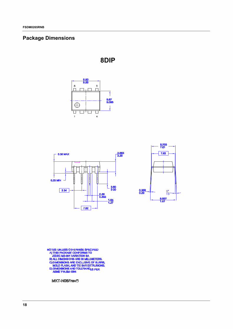
Package Dimensions
8DIP

FSDM0265RNB
19
Ordering Information
Product Number Package Marking Code BVDSS fOSC RDS(ON)FSDM0265RNB 8DIP DM0265R 650V 67KHz 5.0Ω
FSDM0265RNB
9/29/05 0.0m 001© 2005 Fairchild Semiconductor Corporation
LIFE SUPPORT POLICY FAIRCHILD’S PRODUCTS ARE NOT AUTHORIZED FOR USE AS CRITICAL COMPONENTS IN LIFE SUPPORT DEVICES OR SYSTEMS WITHOUT THE EXPRESS WRITTEN APPROVAL OF THE PRESIDENT OF FAIRCHILD SEMICONDUCTOR CORPORATION. As used herein:
1. Life support devices or systems are devices or systems which, (a) are intended for surgical implant into the body, or (b) support or sustain life, and (c) whose failure to perform when properly used in accordance with instructions for use provided in the labeling, can be reasonably expected to result in a significant injury of the user.
2. A critical component in any component of a life support device or system whose failure to perform can be reasonably expected to cause the failure of the life support device or system, or to affect its safety or effectiveness.
www.fairchildsemi.com
DISCLAIMERFAIRCHILD SEMICONDUCTOR RESERVES THE RIGHT TO MAKE CHANGES WITHOUT FURTHER NOTICE TO ANY PRODUCTS HEREIN TO IMPROVE RELIABILITY, FUNCTION OR DESIGN. FAIRCHILD DOES NOT ASSUME ANY LIABILITY ARISING OUT OF THE APPLICATION OR USE OF ANY PRODUCT OR CIRCUIT DESCRIBED HEREIN; NEITHER DOES IT CONVEY ANY LICENSE UNDER ITS PATENT RIGHTS, NOR THE RIGHTS OF OTHERS.