fsd210 - nxpradiodetali.nxp.com.ua/pdf/fsd210.pdf · fsd210 3 electrical characteristics (ta=25°c...
TRANSCRIPT
©2003 Fairchild Semiconductor Corporation
www.fairchildsemi.com
Rev.1.0.0
Features• Single Chip 700V SenseFET Power Switch• Precision Fixed Operating Frequency (134kHz)• Consumes under 0.1W at 265VAC at no load with an
Advanced Burst-Mode Operation• Internal Start-up Switch and Soft Start• UVLO with Hysteresis (6.7V/8.7V)• Pulse by Pulse Current Limit• Over Load Protection • Internal Thermal Shutdown Function (Hysteresis)• Secondary Side Regulation• Auto-Restart Mode• Frequency Modulation for EMI
Applications• Charger & Adaptor for Mobile Phone, PDA & MP3 • Auxiliary Power for PC, C-TV & Monitor
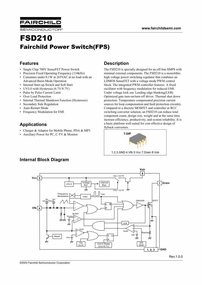
Description The FSD210 is specially designed for an off-line SMPS with minimal external components. The FSD210 is a monolithic high voltage power switching regulator that combines an LDMOS SenseFET with a voltage mode PWM control block. The integrated PWM controller features: A fixed oscillator with frequency modulation for reduced EMI. Under voltage lock out. Leading edge blanking(LEB).Optimized gate turn-on/turn-off driver. Thermal shut down protection. Temperature compensated precision currentsources for loop compensation and fault protection circuitry. Compared to a discrete MOSFET and controller or RCC switching converter solution, an FSD210 can reduce total component count, design size, weight and at the same time increase efficiency, productivity, and system reliability. It is a basic platform well suited for cost effective design of flyback converters.
1.2.3.GND 4.Vfb 5.Vcc 7.Drain 8.Vstr
7-DIP
Internal Block Diagram
8
5
UVLOVoltage
Ref.
Vcc < 6.7V
Vstr
VccInternal
Bias
Vcc > 8.7V
RsenseIover
S/S3mS
4
1, 2, 3
7
OSC
S
R
Q
TSDHis 50
S
R
Q
LEB
OLP
Reset
UVLO Reset(Vcc<6.7V)
DRIVER
FrequencyModulation
5uA 250uA
Vck
Vth
SFET
Drain
GND
Vfb
BURST
VSD
VBURST
FSD210Fairchild Power Switch(FPS)
FSD210
2
Absolute Maximum Ratings(Ta=25°C unless otherwise specified)
Pin Definitions
Parameter Symbol Value UnitMaximum Vstr Pin Voltage Vstr,max 700 VMaximum Supply Voltage VCC,MAX 20 VInput Voltage Range VFB −0.3 to VSD VOperating Ambient Temperature TA −25 to +85 °CStorage Temperature Range TSTG −55 to +150 °C
Pin Number Pin Name Pin Function Description1, 2, 3 GND These pins are the control ground and the SenseFET Source.
4 Vfb
This pin is the inverting input of the PWM comparator. It operates normallybetween 0.5V and 2.5V. It has a 0.25mA current source connected internally and a capacitor and opto coupler connected externally. A feedback voltage of 3V to 4V triggers overload protection (OLP). There is a time delay due to the 5uA current source, which prevents false triggering under transient conditions but still allows the protection mechanism to operate under true overload conditions.
5 Vcc
This is the positive supply voltage input. During start up, current is suppliedto this pin from Pin 7 via an internal switch. When Vcc reaches the UVLOupper threshold (8.7V), the internal switch start-up switch (Vstr) opens andpower is supplied from auxiliary transformer winding.
7 Drain This pin is designed to directly drive the converter transformer and is capable of switching a maximum of 700V.
8 Vstr
This pin connects directly to the rectified AC line voltage source. At start upthe internal switch supplies internal bias and charges an external capacitorthat connects from the Vcc pin to ground. once this reaches 8.7V, the internal current source is disabled.
FSD210
3
Electrical Characteristics(Ta=25°C unless otherwise specified)
Note:1. These parameters, although guaranteed, are not 100% tested in production
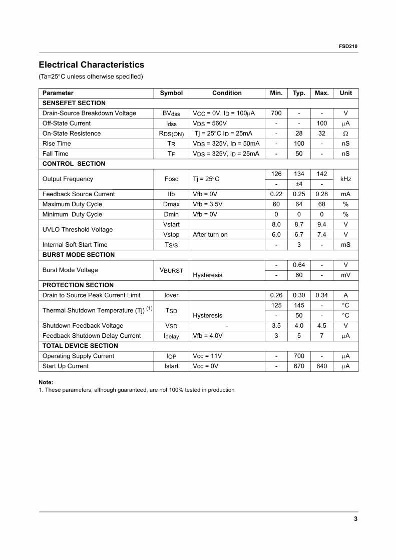
Parameter Symbol Condition Min. Typ. Max. UnitSENSEFET SECTIONDrain-Source Breakdown Voltage BVdss VCC = 0V, ID = 100µA 700 - - VOff-State Current Idss VDS = 560V - - 100 µAOn-State Resistence RDS(ON) Tj = 25°C ID = 25mA - 28 32 Ω
Rise Time TR VDS = 325V, ID = 50mA - 100 - nSFall Time TF VDS = 325V, lD = 25mA - 50 - nSCONTROL SECTION
Output Frequency Fosc Tj = 25°C126 134 142
kHz- ±4 -
Feedback Source Current Ifb Vfb = 0V 0.22 0.25 0.28 mAMaximum Duty Cycle Dmax Vfb = 3.5V 60 64 68 %Minimum Duty Cycle Dmin Vfb = 0V 0 0 0 %
UVLO Threshold VoltageVstart 8.0 8.7 9.4 VVstop After turn on 6.0 6.7 7.4 V
Internal Soft Start Time TS/S - 3 - mSBURST MODE SECTION
Burst Mode Voltage VBURSTHysteresis
- 0.64 - V- 60 - mV
PROTECTION SECTIONDrain to Source Peak Current Limit Iover 0.26 0.30 0.34 A
Thermal Shutdown Temperature (Tj) (1) TSDHysteresis
125 145 - °C- 50 - °C
Shutdown Feedback Voltage VSD - 3.5 4.0 4.5 VFeedback Shutdown Delay Current Idelay Vfb = 4.0V 3 5 7 µATOTAL DEVICE SECTIONOperating Supply Current IOP Vcc = 11V - 700 - µAStart Up Current Istart Vcc = 0V - 670 840 µA
FSD210
4
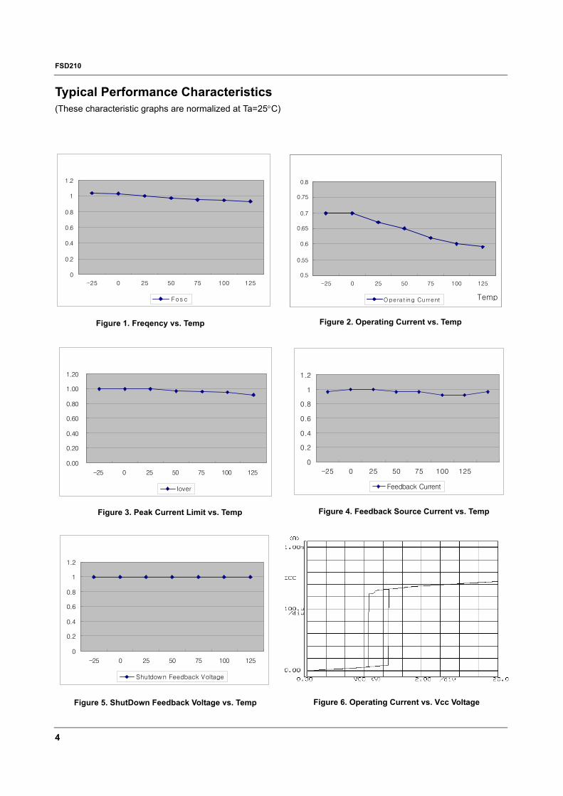
Typical Performance Characteristics(These characteristic graphs are normalized at Ta=25°C)
Under Voltage Lockout (FSD210)Under Voltage Lockout (FSD210)Under Voltage Lockout (FSD210)
Figure 1. Freqency vs. Temp Figure 2. Operating Current vs. Temp
O perating Cur rent
0.5
0.55
0.6
0.65
0.7
0.75
0.8
-25 0 25 50 75 100 125
O perat ing Cu rrent Temp
O perating Cur rent
0.5
0.55
0.6
0.65
0.7
0.75
0.8
-25 0 25 50 75 100 125
O perat ing Cu rrent Temp
Ou tpu t Frequency
0
0.2
0.4
0.6
0.8
1
1.2
-25 0 25 50 75 100 125
Fos c
Figure 3. Peak Current Limit vs. Temp Figure 4. Feedback Source Current vs. Temp
Over Current
0.00
0.20
0.40
0.60
0.80
1.00
1.20
-25 0 25 50 75 100 125
Iover
Feedback Current
0
0.2
0.4
0.6
0.8
1
1.2
-25 0 25 50 75 100 125
Feedback Current
Figure 5. ShutDown Feedback Voltage vs. Temp
Shutdown Feedback Voltage
0
0.2
0.4
0.6
0.8
1
1.2
-25 0 25 50 75 100 125
Shutdown Feedback Voltage
Figure 6. Operating Current vs. Vcc Voltage
FSD210
5
Typical Performance Characteristics (Continued)
(These characteristic graphs are normalized at Ta=25°C)
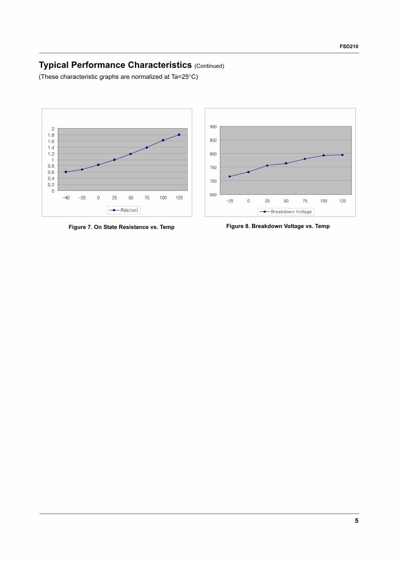
Figure 7. On State Resistance vs. Temp Figure 8. Breakdown Voltage vs. Temp
On_State_Resistance
0
0.2
0.4
0.6
0.81
1.2
1.4
1.6
1.8
2
-40 -25 0 25 50 75 100 125
Rds(on)
Breakdown Voltage
650
700
750
800
850
900
-25 0 25 50 75 100 125
Breakdown Voltage
FSD210
6
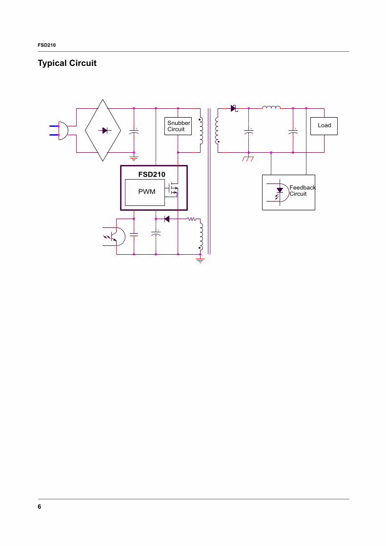
Typical Circuit
PWM
Load+
FeedbackCircuit
SnubberCircuit+ +
FSD210
+
FSD210
7
Product InformationBasic system topology of FSD200/210 is the same as the original FSDH565/0165 devices. The FSD210 devices require a bias winding, whereas the FSD200 devices do not. Other features of the two types of devices are almost the same and are listed below.
Figure 1. Line-up Table
Functional Description
1. Startup : At startup, an internal high voltage current source supplies the internal bias and charges the external Vcc capacitor as shown in Figure 1. In the case of the FSD210, when Vcc reaches 8.7V the device starts switching and the internal high voltage current source is disabled. The device continues to switch provided that Vcc does not drop below 6.7V. After startup the bias is supplied from the auxiliary transformer winding. In the case of FSD200, Vcc is continuously supplied from the external high voltage source and Vcc is regulated to 7V by an internal high voltage regulator (HV Reg). The internal startup switch is not disabled and an auxiliary winding is not required. Figure 2.
Figure 2. Internal startup circuit
2. Feedback Control : The FSD200/210 are voltage mode devices as shown in Figure 3. Usually, an opto-coupler and KA431 type voltage reference are used to implement the feedbacknetwork. The feedback voltage is compared with an internally generated sawtooth waveform. This directly controls the duty cycle. When
the KA431 reference pin voltage exceeds the internal reference voltage of 2.5V, the optocoupler LED current increase pulling down the feedback voltage and reducing the duty cycle. This will happen when the input voltage increases or the output load decreases.
3. Leading edge blanking (LEB) : When the MOSFET turns on, there will usually be a large current spike through the MOSFET. This is caused by primary side capacitance and secondary side rectifier reverse recovery. This could cause premature termination of the switching pulse if it exceeded the over-currentthreshold. Therefore, the FPS uses a leading edgeblanking (LEB) circuit. This circuit inhibits the pver-current comparator for a short time after the MOSFET is turned on.
Figure 3. PWM and feedback circuit
4. Protection Circuit : The FSD200/210 has 2 self protection functions: over-load protection (OLP) and thermal shutdown (TSD). Because these protection circuits are fully integrated into the IC with no external components, system reliability is improved without cost increase. If either of these functions are triggered, the FPS starts an auto-restart cycle. Once the fault condition occurs, switching is terminated and the MOSFET remains off. This cause Vcc to fall. When Vcc reaches the UVLO stop voltage (6.7:FSD210, 6V:FSD200), the protection is reset and the internal high voltage current source charges the Vcc capacitor. When Vcc reaches the UVLO start voltage (8.7V:FSD210, 7V:FSD200), the device attempts toresume normal operation. If the fault condition is no longer present start up will be successful. If it is stillpresent the cycle is repeated. This is shown in Figure 4.
ooooBurst function
145(Hys 50)145(Hys 50)145(Hys 50)145(Hys 50)Thermal Shutdown(typ.)
6W4W6W4W85~265VACOutput Power
Package Type
Operating Current (max)
Frequency Modulation
Switching Frequency
Current Limit (typ.Iover)
On-state Resistance (max)
Breakdown voltage (min)
Product Parameter
7DIP/7SMD7DIP/7SMD7DIP/7SMD7DIP/7SMD
Without Bias WindingWith Bias Winding
770uA770uA770uA770uA
134kHz134kHz134kHz134kHz
±4kHz
0.3A
32ohm
700VBCDMOS
FSD200
±4kHz
0.3A
32ohm
700VBCDMOS
FSD210
±4kHz
0.48A
18ohm
700VBCDMOS
FSD211
18ohm
±4kHz
0.48A
700VBCDMOS
FSD201
Vin,dc
Vstr
Vcc HVReg.
Vin,dc
Vstr
Vcc
7VVcc>8.7V
off
Vcc<6.7Von
Istr Istr
FSD21x FSD20x
4
OSCVcc Vref
5uA 0.25mA
VSD
R
FB Gatedriver
OLP
Vfb
KA431
Cfb
Vo
FSD210
8
Figure 4. Protection block
4.1 Over Load Protection (OLP) : Overload is a load current that exceeds a pre-set level due to an abnormal situation. If this occurs, the protection circuit should be triggered to protect the SMPS. It is possible that a short term load transient can occur under normal operation. If this occurs the system should not shut down. In order to avoid false shut-downs, the over load protection circuit is designed to trigger after a delay. Therefore the device can discriminate between transient overloads and true faul conditions. The device is pulse-by-pulse current limited and therefore, for a given input voltage, the maximum input power is limited. If the load tries to draw more than this, the output voltage will drop below its set value. This reduces the opto-coupler LED current which in turn will reduce the photo-transistorcurrent. Therefore, the 250uA current source will charge the feedback pin capacitor, Cfb, and the feedback voltage, Vfb, will increase. The input to the feedback comparator is clamped at around 3V. Therefore, once Vfb reaches 3V, the device is switching at maximum power. At this point the 250uA current source is blocked and the 5uA source continues to charge Cfb. Once Vfb reaches 4V, switching stops. Therefore the shutdown delay time is set by the time required to charge Cfb from 3V to 4V with 5uA as shown in Fig. 5.
Figure 5. Over load protection delay
4.2 Thermal Shutdown (TSD) : The SenseFET and the control IC are assembled in one package. This makes it easy for the control IC to detect the temperature of the SenseFET. When the temperatureexceeds approximately 150°C, thermal shutdown isactivated. Thermal shutdown has a Hysteresis of 50°C and so the temperature must drop to 100°C before the device attempts to restart.
5. Soft Start : FSD200/210 has an internal soft start circuit that increases the feedback voltage together with the MOSFET current slowly at start up. The soft start time is 3msec in FSD200/210.
OSC
4Vfb
S
R
Q GATEDRIVER
FSD2xxOLP, TSD
Protection Block
5uA 250uA
RESET Vth 4V
OLP
+-
TSDHis 50
S
R
Q
/8
Cfb3VR
Vfb
t
3V
OLP4V
t1 t3
10V
t1<<t2, t3t1 = -1/RC Χ ln( 1-v(t1)/R ) v(t1)=3Vt2 = C Χ [v(t1+t2)-v(t1)] Χ Idelay [v(t1+t2)-v(t1)]=1V, Idelay=5uA
t2
FPS Switching Area
Idelay (5uA) charges Cfb
TSD - 50
Temperature
t
TSD()
FPS Switching Area
TSD Hysteresis
FSD210
9
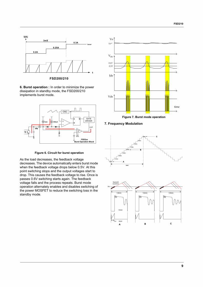
6. Burst operation : In order to minimize the power dissipation in standby mode, the FSD200/210 implements burst mode.
Figure 6. Circuit for burst operation
As the load decreases, the feedback voltage decreases. The device automatically enters burst mode when the feedback voltage drops below 0.5V. At this point switching stops and the output voltages start to drop. This causes the feedback voltage to rise. Once is passes 0.6V switching starts again. The feedback voltage falls and the process repeats. Burst mode operation alternately enables and disables switching of the power MOSFET to reduce the switching loss in the standby mode.
Figure 7. Burst mode operation
7. Frequency Modulation
0.2A
0.25A
0.3A3mS
Iover
FSD200/210
I(A)
t
OSC
4Vfb
S
R
Q GATEDRIVER5uA 250uA
0.6V/0.5V
on/off
FSD2xxBurst Operation Block
VFB
Vds
0.5V0.6V
Ids
VoVoset
time
130kHz
131kHz
132kHz
133kHz
134kHz
135kHz
136kHz
137kHz
138kHz
2mS
A
B
C
130kHz134kHz138kHz
Sawtoothwaveform
Ton
Vfb
Vdrain
Idrain
A B C
FSD210
10
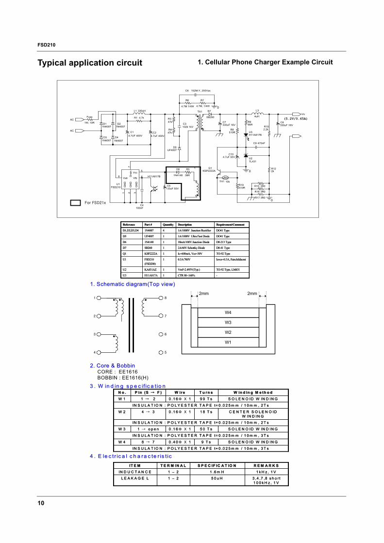
Typical application circuit 1. Cellular Phone Charger Example Circuit
For FSD21x
L3
4uH
C8330uF 16V
L1 330uH
R19510R
R8510R
D6
1N4148
R347k
TH1 10k
Vo
.
R15 3R0
R5
39R
Q1KSP2222A
1
U2TL431
D11N4007
R16 3R0
C9 470nF
TX1
R102.2k
C24.7uF 400V
0
3
C4100nF
H11A817BU3
R1 4.7k
4
C14.7UF 400V
C533uF 50V
7Fuse
1W, 10R
C6 152M-Y, 250Vac
D31N4007
8
H11A817B
2
1
R7
4.7M, 1/4W
AC
R17 3R0
D21N4007
D41N4007
R956R
D5UF4007
AC
0
R122k
C7330uF 16V
(5.2V/0.65A)
R447k
C104.7uF 50V
U1FSD210
8
5
7
1
4
2 3
Vstr
Vcc
Dra
in
GN
D
Vfb
GN
D
GN
D
D7
SB260
R6
4.7M 1/4W 0
C3102k 1kV
TO-92 Type, LM431Vref=2.495V(Typ.)1KA431AZU2
Iover=0.3A, Fairchildsemi0.5A/700V1FSD210(FSD200)
U1
-CTR 80~160%1H11A817AU3
DO41 Type1A/1000V Ultra Fast Diode1UF4007D5
D0-213 Type10mA/100V Junction Diode11N4148D6
D0-41 Type2A/60V Schottky Diode1SB260D7
1
4
Quantity
Ic=600mA, Vce=30V
1A/1000V Junction Rectifier
Description
TO-92 TypeKSP2222AQ1
DO41 Type1N4007D1,D2,D3,D4
Requirement/CommentPart #Reference
1. 1. Schematic diagram(Top view)Schematic diagram(Top view)
2. 2. Core & BobbinCore & BobbinCORE : EE1616BOBBIN : EE1616(H)
W4
W3
W2
W1
2mm 2mm1
2
3
4
8
7
6
5
3 . 3 . W in d in g s p e c if ic a t io nW in d in g s p e c if ic a t io n
4 . 4 . E le c tr ic a l c h a ra c te r is t icE le c tr ic a l c h a ra c te r is t icIN S U L A T IO N : P O L Y E S T E R T A P E t= 0 .0 2 5 m m / 1 0 m m , 3 T s
S O L E N O ID W IN D IN G9 T s0 .4 0 Φ Χ 18 → 7W 4
IN S U L A T IO N : P O L Y E S T E R T A P E t= 0 .0 2 5 m m / 1 0 m m , 3 T s
S O L E N O ID W IN D IN G5 0 T s0 .1 6 Φ Χ 11 → o p e nW 3
IN S U L A T IO N : P O L Y E S T E R T A P E t= 0 .0 2 5 m m / 1 0 m m , 2 T s
C E N T E R S O L E N O ID W IN D IN G
1 8 T s0 .1 6 Φ Χ 14 → 3W 2
IN S U L A T IO N : P O L Y E S T E R T A P E t= 0 .0 2 5 m m / 1 0 m m , 2 T s
S O L E N O ID W IN D IN G9 9 T s0 .1 6 Φ Χ 11 → 2W 1W in d in g M e th o dW in d in g M e th o dT u r n sT u r n sW ir eW ir eP in (S P in (S →→ F )F )N o .N o .
IN S U L A T IO N : P O L Y E S T E R T A P E t= 0 .0 2 5 m m / 1 0 m m , 3 T s
S O L E N O ID W IN D IN G9 T s0 .4 0 Φ Χ 18 → 7W 4
IN S U L A T IO N : P O L Y E S T E R T A P E t= 0 .0 2 5 m m / 1 0 m m , 3 T s
S O L E N O ID W IN D IN G5 0 T s0 .1 6 Φ Χ 11 → o p e nW 3
IN S U L A T IO N : P O L Y E S T E R T A P E t= 0 .0 2 5 m m / 1 0 m m , 2 T s
C E N T E R S O L E N O ID W IN D IN G
1 8 T s0 .1 6 Φ Χ 14 → 3W 2
IN S U L A T IO N : P O L Y E S T E R T A P E t= 0 .0 2 5 m m / 1 0 m m , 2 T s
S O L E N O ID W IN D IN G9 9 T s0 .1 6 Φ Χ 11 → 2W 1W in d in g M e th o dW in d in g M e th o dT u r n sT u r n sW ir eW ir eP in (S P in (S →→ F )F )N o .N o .
3 ,4 ,7 ,8 s h o r t 1 0 0 k H z , 1 V
5 0 u H1 – 2L E A K A G E L1 k H z , 1 V1 .6 m H1 – 2IN D U C T A N C E
R E M A R K SR E M A R K SS P E C IF IC A T IO NS P E C IF IC A T IO NT E R M IN A LT E R M IN A LIT E MIT E M
3 ,4 ,7 ,8 s h o r t 1 0 0 k H z , 1 V
5 0 u H1 – 2L E A K A G E L1 k H z , 1 V1 .6 m H1 – 2IN D U C T A N C E
R E M A R K SR E M A R K SS P E C IF IC A T IO NS P E C IF IC A T IO NT E R M IN A LT E R M IN A LIT E MIT E M
FSD210
11
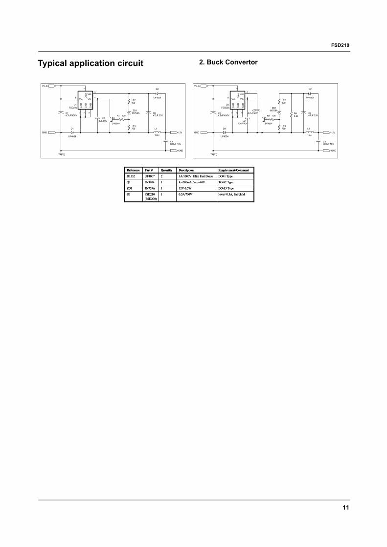
Typical application circuit 2. Buck Convertor
U1FSD21x
8
5
7
1
4
2 3
Vstr
Vcc
Dra
in
GN
D
Vfb
GN
D
GN
D
ZD11N759A
D1
UF4004
Q1
2N3904
R2100
C14.7uF/400V
12VGND
R1 100
C4680uF 16V
Vin,dc
C210uF/50V
GND
C347uF 25V
L1
1mH
R3750
0
D2
UF4004
C210uF/50V
C14.7uF/400V
R45.6k
12VL1
1mH
Q1
2N3904
0
ZD11N759A
Vin,dc
R2100
C54.7uF/50V
C4680uF 16V
GND
GND
R1 100
D1
UF4004
R3750
C347uF 25V
U1FSD20x
8
5
7
1
4
2 3
Vstr
Vcc
Dra
in
GN
D
Vfb
GN
D
GN
D
D2
UF4004
1
1
1
2
Quantity
0.5A/700V
12V 0.5W
Ic=200mA, Vce=40V
1A/1000V Ultra Fast Diode
Description
Iover=0.3A, FairchildFSD210(FSD200)
U1
DO-35 Type1N759AZD1
TO-92 Type2N3904Q1
DO41 TypeUF4007D1,D2
Requirement/CommentPart #Reference
1
1
1
2
Quantity
0.5A/700V
12V 0.5W
Ic=200mA, Vce=40V
1A/1000V Ultra Fast Diode
Description
Iover=0.3A, FairchildFSD210(FSD200)
U1
DO-35 Type1N759AZD1
TO-92 Type2N3904Q1
DO41 TypeUF4007D1,D2
Requirement/CommentPart #Reference
FSD210
12
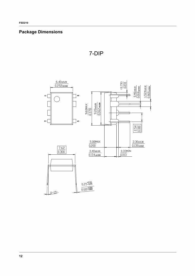
Package Dimensions
7-DIP
FSD210
13
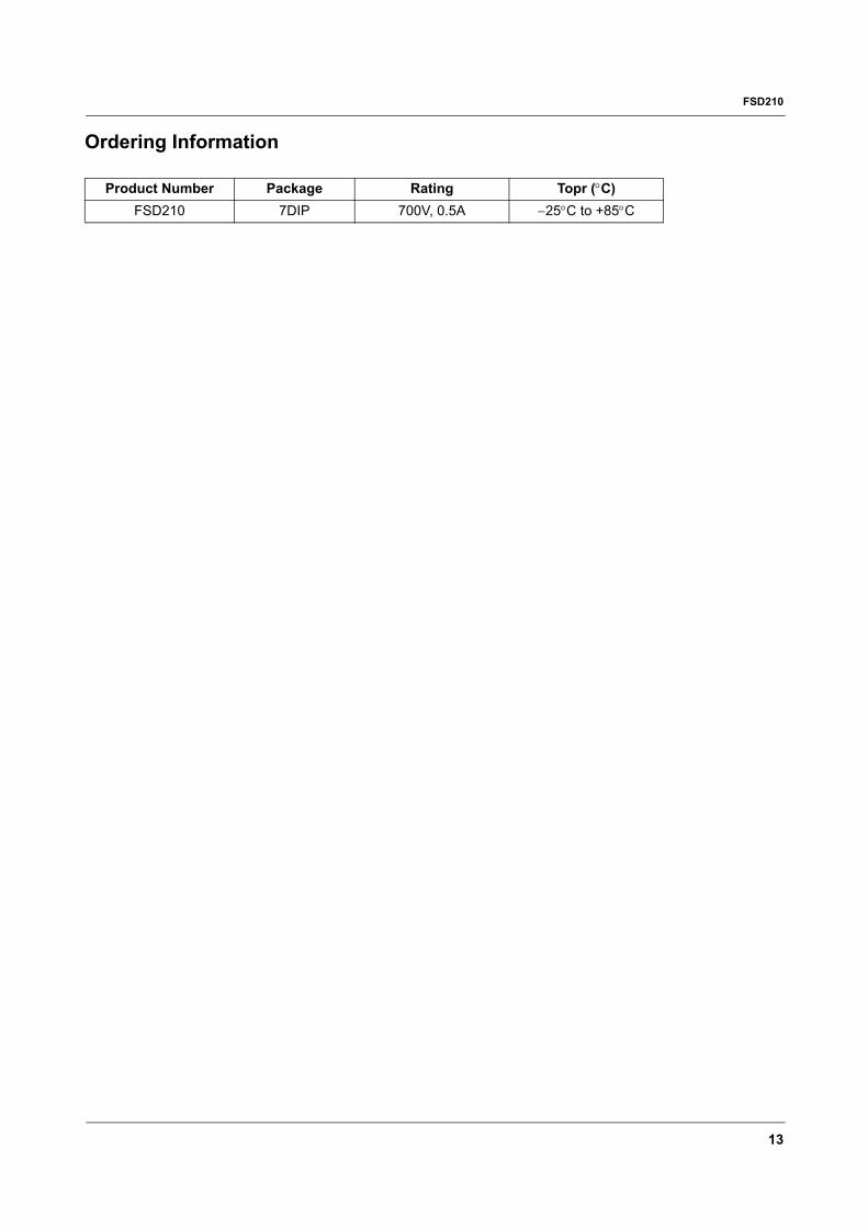
Ordering Information
Product Number Package Rating Topr (°C)FSD210 7DIP 700V, 0.5A −25°C to +85°C
FSD210
8/28/03 0.0m 001Stock#DSxxxxxxxx
2003 Fairchild Semiconductor Corporation
LIFE SUPPORT POLICY FAIRCHILD’S PRODUCTS ARE NOT AUTHORIZED FOR USE AS CRITICAL COMPONENTS IN LIFE SUPPORT DEVICES OR SYSTEMS WITHOUT THE EXPRESS WRITTEN APPROVAL OF THE PRESIDENT OF FAIRCHILD SEMICONDUCTOR CORPORATION. As used herein:
1. Life support devices or systems are devices or systems which, (a) are intended for surgical implant into the body, or (b) support or sustain life, and (c) whose failure to perform when properly used in accordance with instructions for use provided in the labeling, can be reasonably expected to result in a significant injury of the user.
2. A critical component in any component of a life support device or system whose failure to perform can be reasonably expected to cause the failure of the life support device or system, or to affect its safety or effectiveness.
www.fairchildsemi.com
DISCLAIMERFAIRCHILD SEMICONDUCTOR RESERVES THE RIGHT TO MAKE CHANGES WITHOUT FURTHER NOTICE TO ANY PRODUCTS HEREIN TO IMPROVE RELIABILITY, FUNCTION OR DESIGN. FAIRCHILD DOES NOT ASSUME ANY LIABILITY ARISING OUT OF THE APPLICATION OR USE OF ANY PRODUCT OR CIRCUIT DESCRIBED HEREIN; NEITHER DOES IT CONVEY ANY LICENSE UNDER ITS PATENT RIGHTS, NOR THE RIGHTS OF OTHERS.