frontier journal, volume 9, number 5 may 2013 frontier journal
TRANSCRIPT

Frontier Journal, Volume 9, Number 5,May 2013
Frontier JournalFrontier Visionary Interview
Prof. Robert J. Aumann , Hebrew Univ. of Jerusalem, Nobel Laureate in Economics
Prof. A. Michael Spence , Stanford Univ., Nobel Laureate in Economics
Prof. Martin L. Perl , Stanford Univ., Nobel Laureate in Physics
Prof. Frank Wilczek , MIT, Nobel Laureate in Physics
Steve Wozniak , Co-founder, Apple Computer
Vinton G Cerf , Turing Award Winner
Ann Winblad , Co-founder, Hummer Winblad Venture Partners
Richard Stallman , Founder of GNU Project
Jim Rogers , American Investor
Alan Kay , PhD, Turing Award Winner
Prof. Bjarne Stroustrup , Man behind C++, Texas A & M Univ.
Brian Behlendorf , Co-founder of Apache Project
Rajeev Madhavan , Co-founder, Chairman & CEO, Magma Design Automation
Jimmy Wales, Founder of Wikipedia
Craig Newmark , Founder of Craigslist.org
Greg Gianforte , Founder & CEO of RightNow Technologies, Inc
Grady Booch , Chief Scientist, IBM Rational
Aart de Geus , PhD, Co-founder, Chairman & CEO, Synopsys Inc
Copyright c 2004 ~ 2011 Inno Inc.
Web Site: http://www.hwswworld.com Tel: 510-573-0322
39120 Argonaut Way, Ste. 536, Fremont, CA 94538, USA
Simple Op Amp Measurements
By James M Bryant
Op amps are very high gain amplifiers with differential inputs and single-ended outputs. They are often used in high precision analog circuits, so it is important to measure their performance accurately. But in open-loop measurements their high open-loop gain, which may be as great as 107 or more, makes it very hard to avoid errors from very small voltages at the amplifier input due to pickup, stray currents, or the Seebeck (thermocouple) effect.
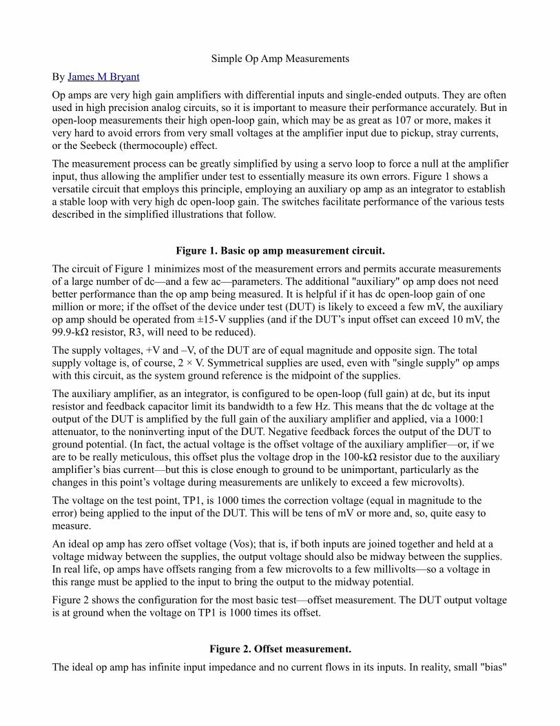
The measurement process can be greatly simplified by using a servo loop to force a null at the amplifier input, thus allowing the amplifier under test to essentially measure its own errors. Figure 1 shows a versatile circuit that employs this principle, employing an auxiliary op amp as an integrator to establish a stable loop with very high dc open-loop gain. The switches facilitate performance of the various tests described in the simplified illustrations that follow.
Figure 1. Basic op amp measurement circuit.The circuit of Figure 1 minimizes most of the measurement errors and permits accurate measurements of a large number of dc—and a few ac—parameters. The additional "auxiliary" op amp does not need better performance than the op amp being measured. It is helpful if it has dc open-loop gain of one million or more; if the offset of the device under test (DUT) is likely to exceed a few mV, the auxiliary op amp should be operated from ±15-V supplies (and if the DUT’s input offset can exceed 10 mV, the 99.9-kΩ resistor, R3, will need to be reduced).
The supply voltages, +V and –V, of the DUT are of equal magnitude and opposite sign. The total supply voltage is, of course, 2 × V. Symmetrical supplies are used, even with "single supply" op amps with this circuit, as the system ground reference is the midpoint of the supplies.
The auxiliary amplifier, as an integrator, is configured to be open-loop (full gain) at dc, but its input resistor and feedback capacitor limit its bandwidth to a few Hz. This means that the dc voltage at the output of the DUT is amplified by the full gain of the auxiliary amplifier and applied, via a 1000:1 attenuator, to the noninverting input of the DUT. Negative feedback forces the output of the DUT to ground potential. (In fact, the actual voltage is the offset voltage of the auxiliary amplifier—or, if we are to be really meticulous, this offset plus the voltage drop in the 100-kΩ resistor due to the auxiliary amplifier’s bias current—but this is close enough to ground to be unimportant, particularly as the changes in this point’s voltage during measurements are unlikely to exceed a few microvolts).
The voltage on the test point, TP1, is 1000 times the correction voltage (equal in magnitude to the error) being applied to the input of the DUT. This will be tens of mV or more and, so, quite easy to measure.
An ideal op amp has zero offset voltage (Vos); that is, if both inputs are joined together and held at a voltage midway between the supplies, the output voltage should also be midway between the supplies. In real life, op amps have offsets ranging from a few microvolts to a few millivolts—so a voltage in this range must be applied to the input to bring the output to the midway potential.
Figure 2 shows the configuration for the most basic test—offset measurement. The DUT output voltage is at ground when the voltage on TP1 is 1000 times its offset.
Figure 2. Offset measurement.The ideal op amp has infinite input impedance and no current flows in its inputs. In reality, small "bias"
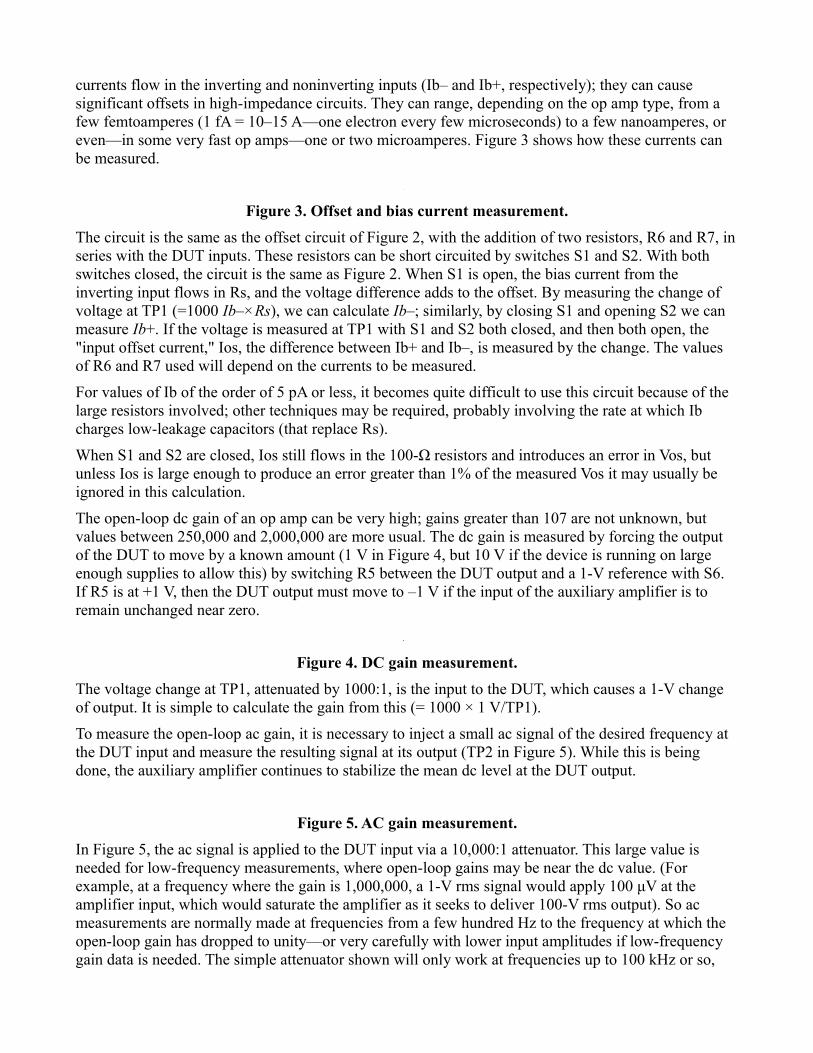
currents flow in the inverting and noninverting inputs (Ib– and Ib+, respectively); they can cause significant offsets in high-impedance circuits. They can range, depending on the op amp type, from a few femtoamperes (1 fA = 10–15 A—one electron every few microseconds) to a few nanoamperes, or even—in some very fast op amps—one or two microamperes. Figure 3 shows how these currents can be measured.
Figure 3. Offset and bias current measurement.The circuit is the same as the offset circuit of Figure 2, with the addition of two resistors, R6 and R7, in series with the DUT inputs. These resistors can be short circuited by switches S1 and S2. With both switches closed, the circuit is the same as Figure 2. When S1 is open, the bias current from the inverting input flows in Rs, and the voltage difference adds to the offset. By measuring the change of voltage at TP1 (=1000 Ib–×Rs), we can calculate Ib–; similarly, by closing S1 and opening S2 we can measure Ib+. If the voltage is measured at TP1 with S1 and S2 both closed, and then both open, the "input offset current," Ios, the difference between Ib+ and Ib–, is measured by the change. The values of R6 and R7 used will depend on the currents to be measured.
For values of Ib of the order of 5 pA or less, it becomes quite difficult to use this circuit because of the large resistors involved; other techniques may be required, probably involving the rate at which Ib charges low-leakage capacitors (that replace Rs).
When S1 and S2 are closed, Ios still flows in the 100-Ω resistors and introduces an error in Vos, but unless Ios is large enough to produce an error greater than 1% of the measured Vos it may usually be ignored in this calculation.
The open-loop dc gain of an op amp can be very high; gains greater than 107 are not unknown, but values between 250,000 and 2,000,000 are more usual. The dc gain is measured by forcing the output of the DUT to move by a known amount (1 V in Figure 4, but 10 V if the device is running on large enough supplies to allow this) by switching R5 between the DUT output and a 1-V reference with S6. If R5 is at +1 V, then the DUT output must move to –1 V if the input of the auxiliary amplifier is to remain unchanged near zero.
Figure 4. DC gain measurement.The voltage change at TP1, attenuated by 1000:1, is the input to the DUT, which causes a 1-V change of output. It is simple to calculate the gain from this (= 1000 × 1 V/TP1).
To measure the open-loop ac gain, it is necessary to inject a small ac signal of the desired frequency at the DUT input and measure the resulting signal at its output (TP2 in Figure 5). While this is being done, the auxiliary amplifier continues to stabilize the mean dc level at the DUT output.
Figure 5. AC gain measurement.In Figure 5, the ac signal is applied to the DUT input via a 10,000:1 attenuator. This large value is needed for low-frequency measurements, where open-loop gains may be near the dc value. (For example, at a frequency where the gain is 1,000,000, a 1-V rms signal would apply 100 μV at the amplifier input, which would saturate the amplifier as it seeks to deliver 100-V rms output). So ac measurements are normally made at frequencies from a few hundred Hz to the frequency at which the open-loop gain has dropped to unity—or very carefully with lower input amplitudes if low-frequency gain data is needed. The simple attenuator shown will only work at frequencies up to 100 kHz or so,
even if great care is taken with stray capacitance; at higher frequencies a more complex circuit would be needed.
The common-mode rejection ratio (CMRR) of an op amp is the ratio of apparent change of offset resulting from a change of common-mode voltage to the applied change of common-mode voltage. It is often of the order of 80 dB to 120 dB at dc, but lower at higher frequencies.
The test circuit is ideally suited to measuring CMRR (Figure 6). The common-mode voltage is not applied to the DUT input terminals, where low-level effects would be likely to disrupt the measurement, but the power-supply voltages are altered (in the same—i.e., common—direction, relative to the input), while the remainder of the circuit is left undisturbed.
Figure 6. DC CMRR measurement.In the circuit of Figure 6, the offset is measured at TP1 with supplies of ±V (in the example, +2.5 V and –2.5 V) and again with both supplies moved up by +1 V to +3.5 V and –1.5 V). The change of offset corresponds to a change of common mode of 1 V, so the dc CMRR is the ratio of the offset change and 1 V.
CMRR refers to change of offset for a change of common mode, the total power supply voltage being unchanged. The power-supply rejection ratio (PSRR), on the other hand, is the ratio of the change of offset to the change of total power supply voltage, with the common-mode voltage being unchanged at the midpoint of the supply (Figure 7).
Figure 7. DC PSRR measurement.The circuit used is exactly the same; the difference is that the total supply voltage is changed, while the common level is unchanged. Here the switch is from +2.5 V and –2.5 V to +3 V and –3 V, a change of total supply voltage from 5 V to 6 V. The common-mode voltage remains at the midpoint. The calculation is the same, too (1000 × TP1/1 V).
To measure ac CMRR and PSRR, the supply voltages are modulated with voltages, as shown in Figure 8 and Figure 9. The DUT continues to operate open-loop at dc, but ac negative feedback defines an exact gain (×100 in the diagrams).
Figure 8. AC CMRR measurement.To measure ac CMRR, the positive and negative supplies to the DUT are modulated with ac voltages with amplitude of 1-V peak. The modulation of both supplies is the same phase, so that the actual supply voltage is steady dc, but the common-mode voltage is a sine wave of 2V p-p, which causes the DUT output to contain an ac voltage, which is measured at TP2.
If the ac voltage at TP2 has an amplitude of x volts peak (2x volts peak-to-peak), then the CMRR, referred to the DUT input (that is, before the ×100 ac gain) is x/100 V, and the CMRR is the ratio of this to 1 V peak.
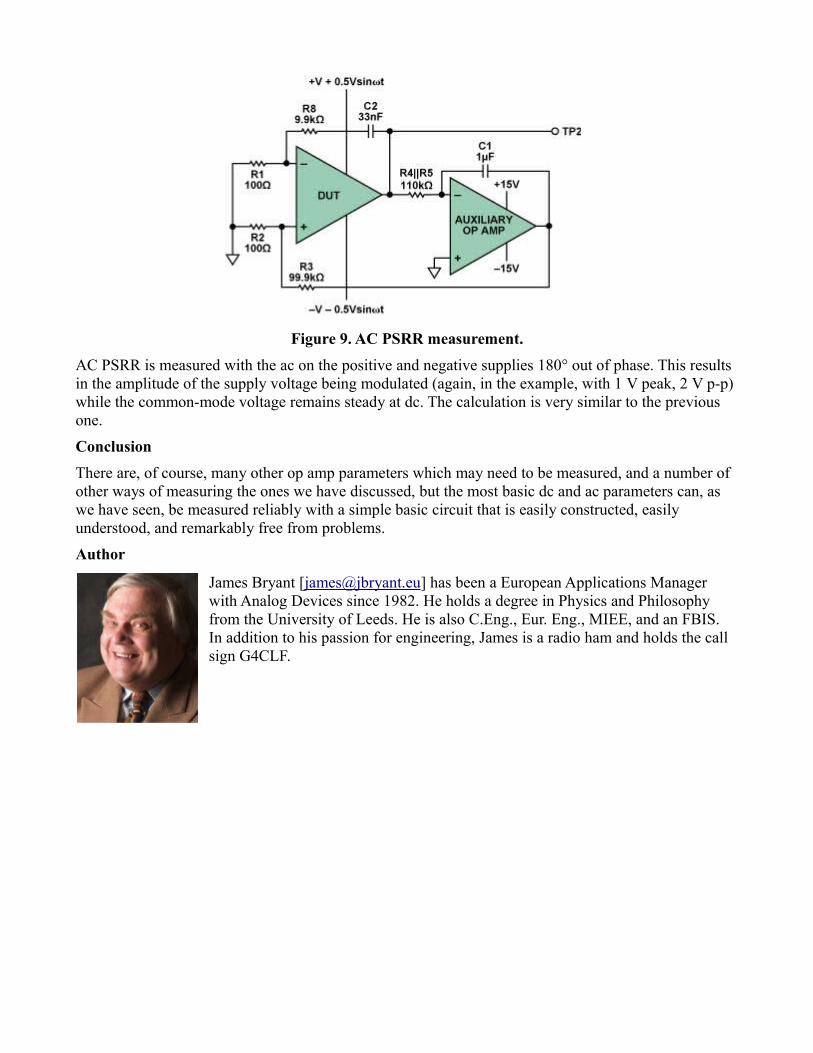
Figure 9. AC PSRR measurement.AC PSRR is measured with the ac on the positive and negative supplies 180° out of phase. This results in the amplitude of the supply voltage being modulated (again, in the example, with 1 V peak, 2 V p-p) while the common-mode voltage remains steady at dc. The calculation is very similar to the previous one.
ConclusionThere are, of course, many other op amp parameters which may need to be measured, and a number of other ways of measuring the ones we have discussed, but the most basic dc and ac parameters can, as we have seen, be measured reliably with a simple basic circuit that is easily constructed, easily understood, and remarkably free from problems.
Author
James Bryant [[email protected]] has been a European Applications Manager with Analog Devices since 1982. He holds a degree in Physics and Philosophy from the University of Leeds. He is also C.Eng., Eur. Eng., MIEE, and an FBIS. In addition to his passion for engineering, James is a radio ham and holds the call sign G4CLF.

Ask The Applications Engineer–40Switch and Multiplexer Design Considerations for Hostile Environments
By Michael Manning
IntroductionHostile environments found in automotive, military, and avionic applications push integrated circuits to their technological limits, requiring them to withstand high voltage and current, extreme temperature and humidity, vibration, radiation, and a variety of other stresses. Systems engineers are rapidly adopting high-performance electronics to provide features and functions in application areas such as safety, entertainment, telematics, control, and human-machine interfaces. The increased use of precision electronics comes at the price of higher system complexity and greater vulnerability to electrical disturbances including overvoltages, latch-up conditions, and electrostatic discharge (ESD) events. Because electronic circuits used in these applications require high reliability and high tolerance to system faults, designers must consider both the environment and the limitations of the components that they choose.
In addition, manufacturers specify absolute maximum ratings for every integrated circuit; these ratings must be observed in order to maintain reliable operation and meet published specifications. When absolute maximum ratings are exceeded, operational parameters cannot be guaranteed; and even internal protections against ESD, overvoltage, or latch-up can fail, resulting in device (and potentially further) damage or failure.
This article describes challenges engineers face when designing analog switches and multiplexers into modules used in hostile environments, and provides suggestions for general solutions that circuit designers can use to protect vulnerable parts. It also introduces some new integrated switches and multiplexers that provide increased overvoltage protection, latch-up immunity, and fault protection to deal with common stress conditions.
Standard Analog Switch ArchitectureTo fully understand the effects of fault conditions on an analog switch, we must first look at its internal structure and operational limits.
A standard CMOS switch (Figure 1) uses both N- and P-channel MOSFETs for the switch element, digital control logic, and driver circuitry. Connecting N- and P-channel MOSFETs in parallel permits bidirectional operation, allowing the analog input voltage to extend to the supply rails, while maintaining fairly constant on resistance over the signal range.
Figure 1. Standard analog switch circuitry.
The source, drain, and logic terminals include clamping diodes to the supplies to provide ESD protection, as illustrated in Figure 1. Reverse-biased in normal operation, the diodes do not pass current unless the signal exceeds the supply voltage. The diodes vary in size, depending on the process, but they are generally kept small to minimize leakage current in normal operation.
The analog switch is controlled as follows: the N-channel device is on for positive gate-to-source voltages and off for negative gate-to-source voltages; the P-channel device is switched by the complementary signal, so it is on at the same time as the N-channel device. The switch is turned on and off by driving the gates to opposite supply rails.
With a fixed voltage on the gate, the effective drive voltage for either transistor varies in proportion to the polarity and magnitude of the analog signal passing through the switch. The dashed lines in Figure 2 show that when the input signal approaches the supplies, the channel of one device or the other will begin to saturate, causing the on resistance of that device to increase sharply. The parallel devices
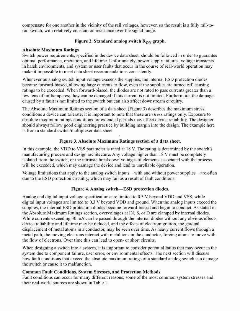
compensate for one another in the vicinity of the rail voltages, however, so the result is a fully rail-to-rail switch, with relatively constant on resistance over the signal range.
Figure 2. Standard analog switch RON graph.
Absolute Maximum RatingsSwitch power requirements, specified in the device data sheet, should be followed in order to guarantee optimal performance, operation, and lifetime. Unfortunately, power supply failures, voltage transients in harsh environments, and system or user faults that occur in the course of real-world operation may make it impossible to meet data sheet recommendations consistently.
Whenever an analog switch input voltage exceeds the supplies, the internal ESD protection diodes become forward-biased, allowing large currents to flow, even if the supplies are turned off, causing ratings to be exceeded. When forward-biased, the diodes are not rated to pass currents greater than a few tens of milliamperes; they can be damaged if this current is not limited. Furthermore, the damage caused by a fault is not limited to the switch but can also affect downstream circuitry.
The Absolute Maximum Ratings section of a data sheet (Figure 3) describes the maximum stress conditions a device can tolerate; it is important to note that these are stress ratings only. Exposure to absolute maximum ratings conditions for extended periods may affect device reliability. The designer should always follow good engineering practice by building margin into the design. The example here is from a standard switch/multiplexer data sheet.
Figure 3. Absolute Maximum Ratings section of a data sheet.
In this example, the VDD to VSS parameter is rated at 18 V. The rating is determined by the switch’s manufacturing process and design architecture. Any voltage higher than 18 V must be completely isolated from the switch, or the intrinsic breakdown voltages of elements associated with the process will be exceeded, which may damage the device and lead to unreliable operation.
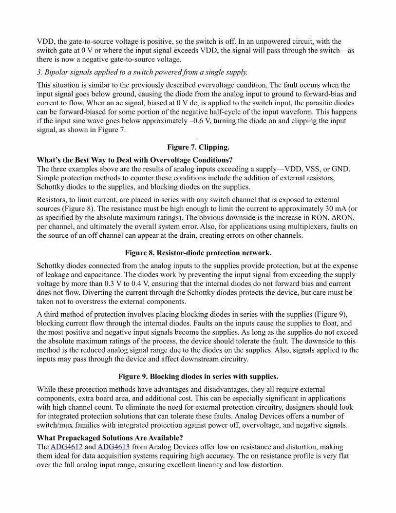
Voltage limitations that apply to the analog switch inputs—with and without power supplies—are often due to the ESD protection circuitry, which may fail as a result of fault conditions.
Figure 4. Analog switch—ESD protection diodes.
Analog and digital input voltage specifications are limited to 0.3 V beyond VDD and VSS, while digital input voltages are limited to 0.3 V beyond VDD and ground. When the analog inputs exceed the supplies, the internal ESD protection diodes become forward-biased and begin to conduct. As stated in the Absolute Maximum Ratings section, overvoltages at IN, S, or D are clamped by internal diodes. While currents exceeding 30 mA can be passed through the internal diodes without any obvious effects, device reliability and lifetime may be reduced, and the effects of electromigration, the gradual displacement of metal atoms in a conductor, may be seen over time. As heavy current flows through a metal path, the moving electrons interact with metal ions in the conductor, forcing atoms to move with the flow of electrons. Over time this can lead to open- or short circuits.
When designing a switch into a system, it is important to consider potential faults that may occur in the system due to component failure, user error, or environmental effects. The next section will discuss how fault conditions that exceed the absolute maximum ratings of a standard analog switch can damage the switch or cause it to malfunction.
Common Fault Conditions, System Stresses, and Protection MethodsFault conditions can occur for many different reasons; some of the most common system stresses and their real-world sources are shown in Table 1:
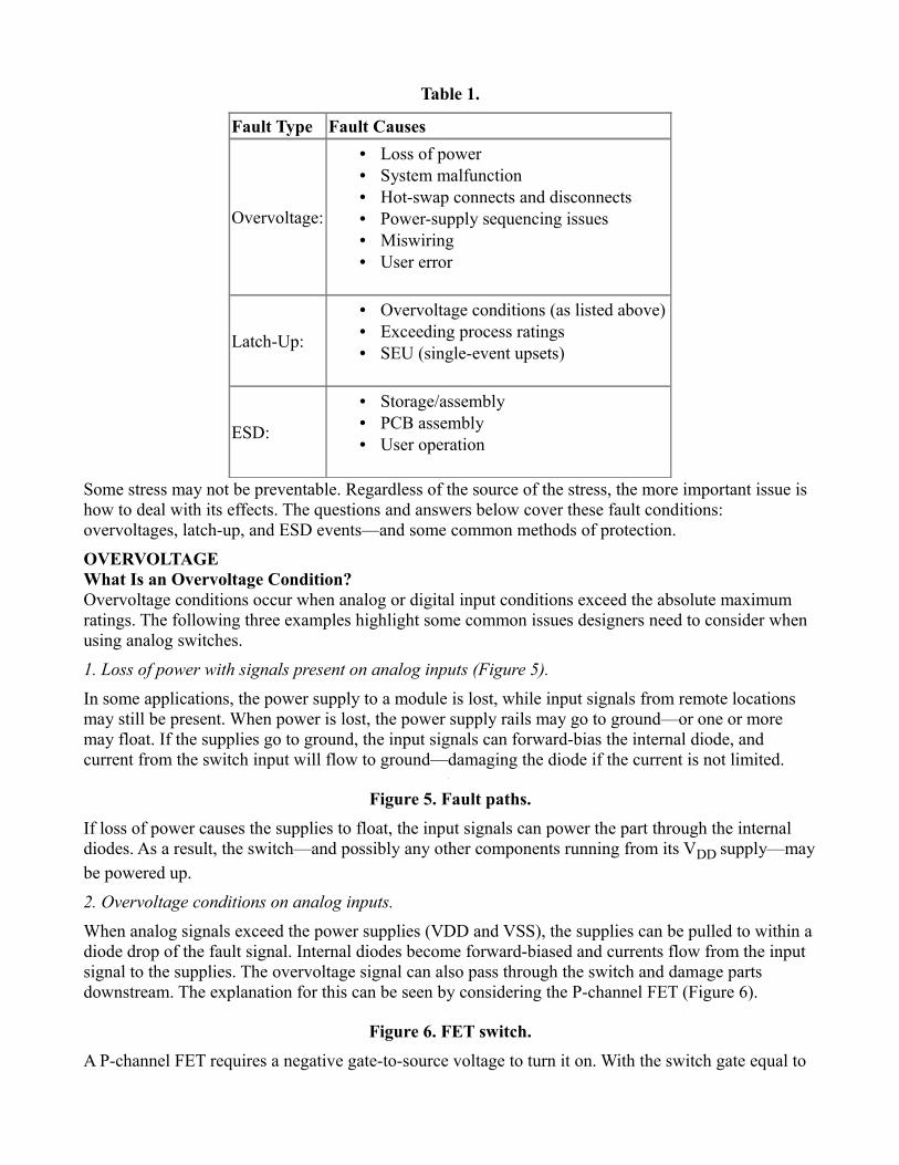
Table 1.
Fault Type Fault Causes
Overvoltage:
• Loss of power • System malfunction • Hot-swap connects and disconnects • Power-supply sequencing issues • Miswiring • User error
Latch-Up:
• Overvoltage conditions (as listed above) • Exceeding process ratings • SEU (single-event upsets)
ESD:
• Storage/assembly • PCB assembly • User operation
Some stress may not be preventable. Regardless of the source of the stress, the more important issue is how to deal with its effects. The questions and answers below cover these fault conditions: overvoltages, latch-up, and ESD events—and some common methods of protection.
OVERVOLTAGEWhat Is an Overvoltage Condition?Overvoltage conditions occur when analog or digital input conditions exceed the absolute maximum ratings. The following three examples highlight some common issues designers need to consider when using analog switches.
1. Loss of power with signals present on analog inputs (Figure 5).In some applications, the power supply to a module is lost, while input signals from remote locations may still be present. When power is lost, the power supply rails may go to ground—or one or more may float. If the supplies go to ground, the input signals can forward-bias the internal diode, and current from the switch input will flow to ground—damaging the diode if the current is not limited.
Figure 5. Fault paths.
If loss of power causes the supplies to float, the input signals can power the part through the internal diodes. As a result, the switch—and possibly any other components running from its VDD supply—may be powered up.
2. Overvoltage conditions on analog inputs.When analog signals exceed the power supplies (VDD and VSS), the supplies can be pulled to within a diode drop of the fault signal. Internal diodes become forward-biased and currents flow from the input signal to the supplies. The overvoltage signal can also pass through the switch and damage parts downstream. The explanation for this can be seen by considering the P-channel FET (Figure 6).
Figure 6. FET switch.
A P-channel FET requires a negative gate-to-source voltage to turn it on. With the switch gate equal to
VDD, the gate-to-source voltage is positive, so the switch is off. In an unpowered circuit, with the switch gate at 0 V or where the input signal exceeds VDD, the signal will pass through the switch—as there is now a negative gate-to-source voltage.
3. Bipolar signals applied to a switch powered from a single supply.This situation is similar to the previously described overvoltage condition. The fault occurs when the input signal goes below ground, causing the diode from the analog input to ground to forward-bias and current to flow. When an ac signal, biased at 0 V dc, is applied to the switch input, the parasitic diodes can be forward-biased for some portion of the negative half-cycle of the input waveform. This happens if the input sine wave goes below approximately –0.6 V, turning the diode on and clipping the input signal, as shown in Figure 7.
Figure 7. Clipping.
What’s the Best Way to Deal with Overvoltage Conditions?The three examples above are the results of analog inputs exceeding a supply—VDD, VSS, or GND. Simple protection methods to counter these conditions include the addition of external resistors, Schottky diodes to the supplies, and blocking diodes on the supplies.
Resistors, to limit current, are placed in series with any switch channel that is exposed to external sources (Figure 8). The resistance must be high enough to limit the current to approximately 30 mA (or as specified by the absolute maximum ratings). The obvious downside is the increase in RON, ∆RON, per channel, and ultimately the overall system error. Also, for applications using multiplexers, faults on the source of an off channel can appear at the drain, creating errors on other channels.
Figure 8. Resistor-diode protection network.
Schottky diodes connected from the analog inputs to the supplies provide protection, but at the expense of leakage and capacitance. The diodes work by preventing the input signal from exceeding the supply voltage by more than 0.3 V to 0.4 V, ensuring that the internal diodes do not forward bias and current does not flow. Diverting the current through the Schottky diodes protects the device, but care must be taken not to overstress the external components.
A third method of protection involves placing blocking diodes in series with the supplies (Figure 9), blocking current flow through the internal diodes. Faults on the inputs cause the supplies to float, and the most positive and negative input signals become the supplies. As long as the supplies do not exceed the absolute maximum ratings of the process, the device should tolerate the fault. The downside to this method is the reduced analog signal range due to the diodes on the supplies. Also, signals applied to the inputs may pass through the device and affect downstream circuitry.
Figure 9. Blocking diodes in series with supplies.
While these protection methods have advantages and disadvantages, they all require external components, extra board area, and additional cost. This can be especially significant in applications with high channel count. To eliminate the need for external protection circuitry, designers should look for integrated protection solutions that can tolerate these faults. Analog Devices offers a number of switch/mux families with integrated protection against power off, overvoltage, and negative signals.
What Prepackaged Solutions Are Available?The ADG4612 and ADG4613 from Analog Devices offer low on resistance and distortion, making them ideal for data acquisition systems requiring high accuracy. The on resistance profile is very flat over the full analog input range, ensuring excellent linearity and low distortion.

The ADG4612 family offers power-off protection, overvoltage protection, and negative-signal handling, all conditions a standard CMOS switch cannot handle.
When no power supplies are present, the switch remains in the off condition. The switch inputs present a high impedance, limiting current flow that could damage the switch or downstream circuitry. This is very useful in applications where analog signals may be present at the switch inputs before the power is turned on, or where the user has no control over the power supply sequence. In the off condition, signal levels up to 16 V are blocked. Also, the switch turns off if the analog input signal level exceeds VDD by VT.
Figure 10. ADG4612/ADG4613 switch architecture.
Figure 10 shows a block diagram of the family’s power-off protection architecture. Switch source- and drain inputs are constantly monitored and compared to the supply voltages, VDD and VSS. In normal operation the switch behaves as a standard CMOS switch with full rail-to-rail operation. However, during a fault condition where the source or drain input exceeds a supply by a threshold voltage, internal fault circuitry senses the overvoltage condition and puts the switch in isolation mode.
Analog Devices also offers multiplexers and channel protectors that can tolerate overvoltage conditions of +40 V/–25 V beyond the supplies with power (±15 V) applied to the device, and +55 V/–40 V unpowered. These devices are specifically designed to handle faults caused by power-off conditions.
Figure 11. High-voltage fault-protected switch architecture.
These devices comprise N-channel, P-channel, and N-channel MOSFETs in series, as illustrated in Figure 11. When one of the analog inputs or outputs exceeds the power supplies, one of the MOSFETs switches off, the multiplexer input (or output) appears as an open circuit, and the output is clamped to within the supply rail, thereby preventing the overvoltage from damaging any circuitry following the multiplexer. This protects the multiplexer, the circuitry it drives, and the sensors or signal sources that drive the multiplexer. When the power supplies are lost (through, for example, battery disconnection or power failure) or momentarily disconnected (rack system, for example), all transistors are off and the current is limited to subnanoampere levels. The ADG508F, ADG509F, and ADG528F include 8:1 and differential 4:1 multiplexers with such functionality.
The ADG465 single- and ADG467 octal channel protectors have the same protective architecture as these fault-protected multiplexers, without the switch function. When powered, the channel is always in the on condition, but in the event of a fault, the output is clamped to within the supply voltages.
LATCH-UPWhat Is a Latch-Up Condition?Latch-up may be defined as the creation of a low-impedance path between power supply rails as a result of triggering a parasitic device. Latch-up occurs in CMOS devices: intrinsic parasitic devices form a PNPN SCR structure when one of the two parasitic base-emitter junctions is momentarily forward-biased (Figure 12). The SCR turns on, causing a continuing short between the supplies. Triggering a latch-up condition is serious: in the “best” case, it leads to device malfunction, with power cycling required to restore the device to normal operation; in the worst case, the device (and possibly power supply) can be destroyed if current flow is not limited.
Figure 12. Parasitic SCR structure: a) device b) equivalent circuit.
The fault and overvoltage conditions described earlier are among the common causes of triggering a latch-up condition. If signals on the analog or digital inputs exceed the supplies, a parasitic transistor is turned on. The collector current of this transistor causes a voltage drop across the base emitter of a

second parasitic transistor, which turns the transistor on, and results in a self-sustaining path between the supplies. Figure 12(b) clearly shows the SCR circuit structure formed between Q1 and Q2.
Events need not last long to trigger latch-up. Short-lived transients, spikes, or ESD events may be enough to cause a device to enter a latch-up state.
Latch-up can also occur when the supply voltages are stressed beyond the absolute maximum ratings of the device, causing internal junctions to break down and the SCR to trigger.
The second triggering mechanism occurs if a supply voltage is raised enough to break down an internal junction, injecting current into the SCR.
What’s the Best Way to Deal with Latch-Up Conditions?Protection methods against latch-up include the same protection methods recommended to address overvoltage conditions. Adding current-limiting resistors in the signal path, Schottky diodes to the supplies, and diodes in series with the supplies—as illustrated in Figure 8 and Figure 9—all help to prevent current from flowing in the parasitic transistors, thereby preventing the SCR from triggering.
Switches with multiple supplies may have additional power-supply sequencing issues that may violate the absolute maximum ratings. Improper supply sequencing can lead to internal diodes turning on and triggering latch-up. External Schottky diodes, connected between supplies, will adequately prevent SCR conduction by ensuring that when multiple supplies are applied to the switch, VDD is always within a diode drop (0.3 V for Schottky) of these supplies, thereby preventing violation of the maximum ratings.
What Prepackaged Solutions Are Available?As an alternative to using external protection, some ICs are manufactured using a process with an epitaxial layer, which increases the substrate- and N-well resistances in the SCR structure. The higher resistance means that a harsher stress is required to trigger the SCR, resulting in a device that is less susceptible to latch-up. An example is the Analog Devices iCMOS® process, which made possible the ADG121x, ADG141x, and ADG161x switch/mux families.
For applications requiring a latch-up proof solution, new trench-isolated switches and multiplexers guarantee latch-up prevention in high-voltage industrial applications operating at up to ±20 V. The ADG541x and ADG521x families are designed for instrumentation, automotive, avionics, and other harsh environments that are likely to foster latch-up. The process uses an insulating oxide layer (trench) placed between the N-channel and the P-channel transistors of each CMOS switch. The oxide layers, both horizontal and vertical, produce complete isolation between devices. Parasitic junctions between transistors in junction-isolated switches are eliminated, resulting in a completely latch-up proof switch.
Figure 13. Trench isolation in latch-up prevention.
The industry practice is to classify the susceptibility of inputs and outputs to latch-up in terms of the amount of excess current an I/O pin can source or sink in the overvoltage condition before the internal parasitic resistances develop enough voltage drop to sustain the latch-up condition.
A value of 100 mA is generally considered adequate. Devices in the ADG5412 latch-up proof family were stressed to ±500 mA with a 1-ms pulse without failure. Latch-up testing at Analog Devices is performed according to EIA/JEDEC-78 (IC Latch-Up Test).
ESD—ELECTROSTATIC DISCHARGEWhat Is an Electrostatic Discharge Event?Typically the most common type of voltage transient that a device is exposed to, ESD, can be defined as a single, fast, high-current transfer of electrostatic charge between two objects at different
electrostatic potentials. We frequently experience this after walking across an insulating surface, such as a rug, storing a charge, and then touching an earthed piece of equipment—resulting in a discharge through the equipment, with high currents flowing in a short space of time.
ICs can be damaged by the high voltages and high peak currents generated by an ESD event. The effects of an ESD event on an analog switch can include reduced reliability over time, the degradation of switch performance, increased channel leakage, or complete device failure.
ESD events can occur at any stage of the life of an IC, from manufacturing through testing, handling, OEM user, and end-user operation. In order to evaluate an IC’s robustness to various ESD events, electrical pulse circuits modeling the following simulated stress environments were identified: human body model (HBM), field-induced charged device model (FICDM), and machine model (MM).
What’s the Best Way to Deal with ESD Events?ESD prevention methods, such as maintaining a static-safe work area, are used to avoid any build up during production, assembly, and storage. These environments, and the individuals working in them, can generally be carefully controlled, but the environments in which the device later finds itself may be anything but controlled.
Analog switch ESD protection is generally in the form of diodes from the analog and digital inputs to the supplies, as well as power supply protection in the form of diodes between the supplies—as illustrated in Figure 14.
Figure 14. Analog switch ESD protection.
The protection diodes clamp voltage transients and divert current to the supplies. The downside of these protection devices is that they add capacitance and leakage to the signal path in normal operation, which may be undesirable in some applications.
For applications that require greater protection against ESD events, discrete components such as Zener diodes, metal-oxide varistors (MOVs), transient voltage suppressors (TVS), and diodes are commonly used. However, they can lead to signal integrity issues due to the extra capacitance and leakage on the signal line; this means design engineers need to carefully consider the trade-off between performance and reliability.
What Prepackaged Solutions Are Available?While the vast majority of ADI switch/mux products meet HBM levels of at least ±2 kV, others go beyond this in robustness, achieving HBM ratings of up to ±8 kV. ADG541x family members have achieved a ±8-kV HBM rating, a ±1.5-kV FICDM rating, and a ±400-V MM rating, making them industry leaders, combining high-voltage performance and robustness.
ConclusionWhen switch or multiplexer inputs come from remotely located sources, there is an increased likelihood that faults can occur. Overvoltage conditions may occur due to systems with poorly designed power-supply sequencing or where hot-plug insertion is a requirement. In harsh electrical environments, transient voltages due to poor connections or inductive coupling may damage components if not protected. Faults can also occur due to power-supply failures where power connections are lost while switch inputs remain exposed to analog signals. Significant damage may result from these fault conditions, possibly causing damage and requiring expensive repairs. While a number of protective design techniques are used to deal with faults, they add extra cost and board area and often require a trade-off in switch performance; and even with external protection implemented, downstream circuitry is not always protected. Since analog switches and multiplexers are often a module’s most likely electronic components to be subjected to a fault, it is important to understand how
they behave when exposed to conditions that exceed the absolute maximum ratings.
Switch/mux products, like devices mentioned here, are available with integrated protection, allowing designers to eliminate external protection circuitry, reducing the number and cost of components in board designs. Savings are even more significant in applications with high channel count.
Ultimately, using switches with fault protection, overvoltage protection, immunity to latch-up, and a high ESD rating yields a robust product that meets industry regulations and enhances customer and end-user satisfaction.
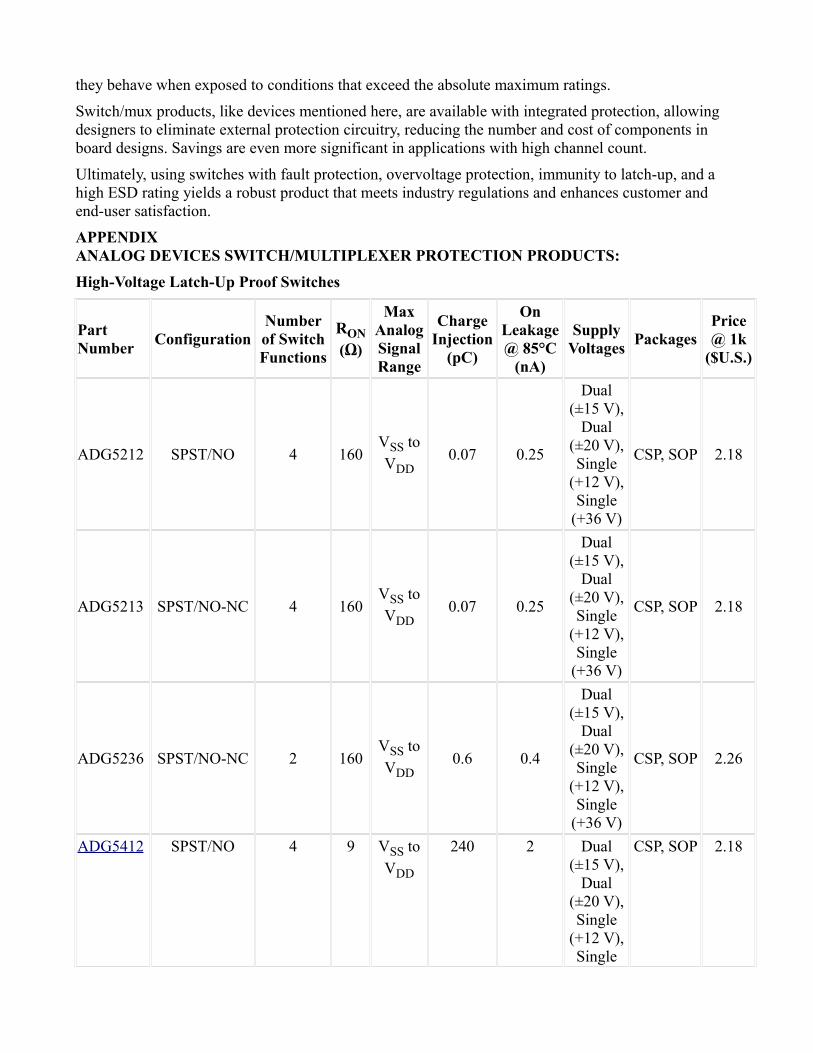
APPENDIX ANALOG DEVICES SWITCH/MULTIPLEXER PROTECTION PRODUCTS:High-Voltage Latch-Up Proof Switches
Part Number Configuration
Number of Switch Functions
RON (Ω)
Max Analog Signal Range
Charge Injection
(pC)
On Leakage @ 85°C
(nA)
Supply Voltages Packages
Price @ 1k
($U.S.)
ADG5212 SPST/NO 4 160VSS to VDD
0.07 0.25
Dual (±15 V),
Dual (±20 V),Single
(+12 V), Single
(+36 V)
CSP, SOP 2.18
ADG5213 SPST/NO-NC 4 160VSS to VDD
0.07 0.25
Dual (±15 V),
Dual (±20 V),Single
(+12 V), Single
(+36 V)
CSP, SOP 2.18
ADG5236 SPST/NO-NC 2 160VSS to VDD
0.6 0.4
Dual (±15 V),
Dual (±20 V),Single
(+12 V), Single
(+36 V)
CSP, SOP 2.26
ADG5412 SPST/NO 4 9 VSS to VDD
240 2 Dual (±15 V),
Dual (±20 V),Single
(+12 V), Single
CSP, SOP 2.18
(+36 V)
ADG5413 SPST/NO-NC 4 9VSS to VDD
240 2
Dual (±15 V),
Dual (±20 V),Single
(+12 V), Single
(+36 V)
CSP, SOP 2.18
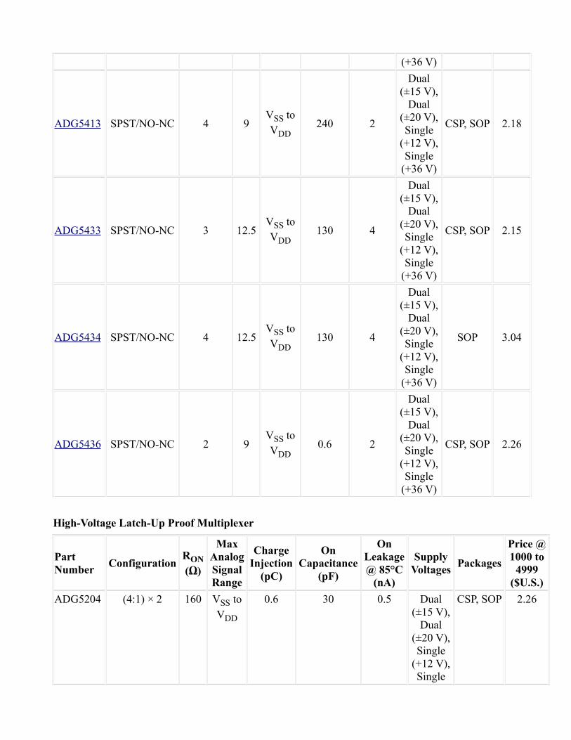
ADG5433 SPST/NO-NC 3 12.5VSS to VDD
130 4
Dual (±15 V),
Dual (±20 V),Single
(+12 V), Single
(+36 V)
CSP, SOP 2.15
ADG5434 SPST/NO-NC 4 12.5VSS to VDD
130 4
Dual (±15 V),
Dual (±20 V),Single
(+12 V), Single
(+36 V)
SOP 3.04
ADG5436 SPST/NO-NC 2 9VSS to VDD
0.6 2
Dual (±15 V),
Dual (±20 V),Single
(+12 V), Single
(+36 V)
CSP, SOP 2.26
High-Voltage Latch-Up Proof Multiplexer
Part Number Configuration
RON (Ω)
Max Analog Signal Range
Charge Injection
(pC)
On Capacitance
(pF)
On Leakage @ 85°C
(nA)
Supply Voltages Packages
Price @ 1000 to
4999($U.S.)
ADG5204 (4:1) × 2 160 VSS to VDD
0.6 30 0.5 Dual (±15 V),
Dual (±20 V),Single
(+12 V), Single
CSP, SOP 2.26
(+36 V)
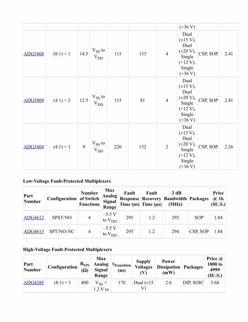
ADG5408 (8:1) × 1 14.5VSS to VDD
115 133 4
Dual (±15 V),
Dual (±20 V),Single
(+12 V), Single
(+36 V)
CSP, SOP 2.41
ADG5409 (4:1) × 2 12.5VSS to VDD
115 81 4
Dual (±15 V),
Dual (±20 V),Single
(+12 V), Single
(+36 V)
CSP, SOP 2.41
ADG5404 (4:1) × 1 9VSS to VDD
220 132 2
Dual (±15 V),
Dual (±20 V),Single
(+12 V), Single
(+36 V)
CSP, SOP 2.26
Low-Voltage Fault-Protected Multiplexers
Part Number Configuration
Number of Switch Functions
Max Analog Signal Range
Fault Response Time (ns)
Fault Recovery Time (µs)
–3 dB Bandwidth
(MHz)Packages
Price @ 1k
($U.S.)
ADG4612 SPST/NO 4–5.5 V to VDD
295 1.2 293 SOP 1.84
ADG4613 SPT/NO-NC 4–5.5 V to VDD
295 1.2 294 CSP, SOP 1.84
High-Voltage Fault-Protected Multiplexers
Part Number Configuration
RON (Ω)
Max Analog Signal Range
tTransition(ns)
Supply Voltages
(V)
Power Dissipation
(mW)Packages
Price @ 1000 to
4999($U.S.)
ADG438F (8:1) × 1 400 VSS + 1.2 V to
170 Dual (±15 V)
2.6 DIP, SOIC 3.68
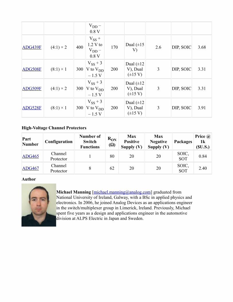
VDD – 0.8 V
ADG439F (4:1) × 2 400
VSS + 1.2 V to VDD – 0.8 V
170 Dual (±15 V) 2.6 DIP, SOIC 3.68
ADG508F (8:1) × 1 300VSS + 3
V to VDD – 1.5 V
200Dual (±12 V), Dual (±15 V)
3 DIP, SOIC 3.31
ADG509F (4:1) × 2 300VSS + 3
V to VDD – 1.5 V
200Dual (±12 V), Dual (±15 V)
3 DIP, SOIC 3.31
ADG528F (8:1) × 1 300VSS + 3
V to VDD – 1.5 V
200Dual (±12 V), Dual (±15 V)
3 DIP, SOIC 3.91
High-Voltage Channel Protectors
Part Number Configuration
Number of Switch
Functions
RON (Ω)
Max Positive
Supply (V)
Max Negative
Supply (V)Packages
Price @ 1k
($U.S.)
ADG465 Channel Protector 1 80 20 20 SOIC,
SOT 0.84
ADG467 Channel Protector 8 62 20 20 SOIC,
SOT 2.40
Author
Michael Manning [[email protected]] graduated from National University of Ireland, Galway, with a BSc in applied physics and electronics. In 2006, he joined Analog Devices as an applications engineer in the switch/multiplexer group in Limerick, Ireland. Previously, Michael spent five years as a design and applications engineer in the automotive division at ALPS Electric in Japan and Sweden.
AD7879 Controller Enables Gesture Recognition on Resistive Touch Screens
By Javier Calpe, Italo Medina, Alberto Carbajo, María José Martínez
An enhanced, low-cost user interface using touch is a valuable feature for a variety of consumer, medical, automotive, and industrial devices. In many consumer applications, designers prefer expensive capacitive touch screens to resistive technologies because they can track a large number of fingers and seem to offer a friendlier interaction with the user. At present, low-cost resistive technologies fill a market niche where only a single touch is required, extremely accurate spatial resolution is paramount, a stylus facilitates specific functionality—such as Asian-language character recognition, or in environments where users must wear gloves.
Although resistive technologies have conventionally been used to detect the position of a single touch on the screen, this article offers a new dual-touch concept that uses the AD7879 resistive touch-screen controller to detect the most common two-finger gestures (zoom, pinch, and rotation) using inexpensive resistive touch screens.
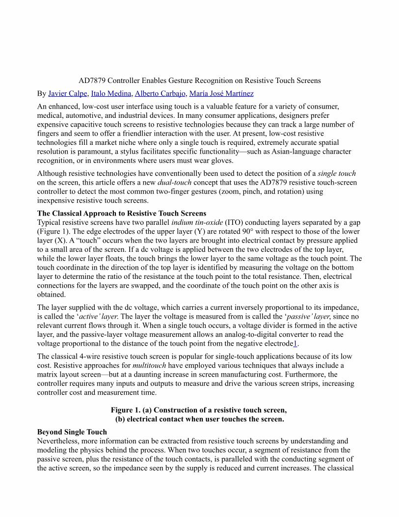
The Classical Approach to Resistive Touch ScreensTypical resistive screens have two parallel indium tin-oxide (ITO) conducting layers separated by a gap (Figure 1). The edge electrodes of the upper layer (Y) are rotated 90° with respect to those of the lower layer (X). A “touch” occurs when the two layers are brought into electrical contact by pressure applied to a small area of the screen. If a dc voltage is applied between the two electrodes of the top layer, while the lower layer floats, the touch brings the lower layer to the same voltage as the touch point. The touch coordinate in the direction of the top layer is identified by measuring the voltage on the bottom layer to determine the ratio of the resistance at the touch point to the total resistance. Then, electrical connections for the layers are swapped, and the coordinate of the touch point on the other axis is obtained.
The layer supplied with the dc voltage, which carries a current inversely proportional to its impedance, is called the ‘active’ layer. The layer the voltage is measured from is called the ‘passive’ layer, since no relevant current flows through it. When a single touch occurs, a voltage divider is formed in the active layer, and the passive-layer voltage measurement allows an analog-to-digital converter to read the voltage proportional to the distance of the touch point from the negative electrode1.
The classical 4-wire resistive touch screen is popular for single-touch applications because of its low cost. Resistive approaches for multitouch have employed various techniques that always include a matrix layout screen—but at a daunting increase in screen manufacturing cost. Furthermore, the controller requires many inputs and outputs to measure and drive the various screen strips, increasing controller cost and measurement time.
Figure 1. (a) Construction of a resistive touch screen,
(b) electrical contact when user touches the screen.Beyond Single TouchNevertheless, more information can be extracted from resistive touch screens by understanding and modeling the physics behind the process. When two touches occur, a segment of resistance from the passive screen, plus the resistance of the touch contacts, is paralleled with the conducting segment of the active screen, so the impedance seen by the supply is reduced and current increases. The classical
approach to resistive controllers assumes that the current through the active layer is constant, and the passive layer is equipotential. With two touches, these assumptions no longer hold, so additional measurements are required to extract the desired information.
A model of dual touch sensing in a resistive screen is shown in Figure 2. Rtouch is the contact resistance between layers; in most of the screens currently available, it is typically of the same order as the resistance of both layers. If a constant current, I, flows through the terminals of the active layer, the voltage across the active layer is as follows:
Figure 2. Basic model of dual touch in resistive screens.
Gesture RecognitionThe idea behind gesture recognition can be better described using a pinch as an example. A pinch gesture starts with touches by two well-separated fingers. This produces a double contact, which reduces the impedance of the screen—and, thus, the voltage difference between the plates of the active layer. As the fingers are brought closer together, the paralleled area decreases, so the impedance of the screen increases, as does the voltage difference between the plates of the active layer.
When tightly pinched, the parallel resistance approaches zero and Ru + Rd increases to the total resistance, so the voltage increases to
Figure 3 shows an example where the pinch is executed along the vertical (Y) axis. The voltage between the electrodes of one of the layers is constant while the other layer shows a step decrease when the gesture starts, followed by an increase as the fingers come closer together.
Figure 3. Voltage measurements when a vertical pinch is performed.
Figure 4 shows the voltage measurements when a pinch is executed at a slant. In this case, both voltages show the step decrease and slow recovery. The ratio between the two recovery rates, normalized by the resistances of each layer, can be used to detect the angle of the gesture.
Figure 4. Voltage measurements when a diagonal pinch is executed.
If the gesture is a zoom (fingers moved apart), the behavior can be deduced from the previous discussion. Figure 5 shows the voltage trends measured in both active layers when zoom gestures are executed along each axis and in an oblique direction.
Figure 5. Voltage trends when zooms are executed in differing directions.
Detecting Gestures with the AD7879The AD7879 touch-screen controller is designed to interface with 4-wire resistive touch screens. In addition to sensing touch, it also measures temperature and the voltage on an auxiliary input. All four touch measurements—along with temperature, battery, and auxiliary voltage measurements—can be programmed into its on-chip sequencer.
The AD7879, accompanied by a pair of low-cost op amps, can perform the above pinch and zoom gesture measurements, as shown in Figure 6.
The following steps describe the procedure to recognize gestures:
1. In the first semi-cycle, a dc voltage is applied to the top (active) layer, and the voltage at the X+ pin (corresponding to VY+ – VY–) is measured. This provides information related to motion (together or apart) in the Y direction.
2. In the second semi-cycle, a dc voltage is applied to the bottom (active) layer, and the voltage at the Y+ pin (corresponding to VX+ – VX–) is measured. This provides information related to motion (together or apart) in the X direction.
The circuit in Figure 6 requires the differential amplifiers to be protected against shorts to VDD. During the first semi-cycle, the output of the lower amplifier is shorted to VDD. During the second semi-cycle, the output of the upper amplifier is shorted to VDD. To avoid this, two external analog switches can be controlled by the AD7879’s GPIO, as shown in Figure 7.
Figure 6. Application diagram for basic gesture detection.
Figure 7. Application diagram that avoids shorting the amplifier outputs to VDD.
In this case, the AD7879 is programmed in slave conversion mode, and only one semi-cycle is measured. When the AD7879 completes the conversion, an interrupt is generated. The host processor reprograms the AD7879 to measure the second semi-cycle and changes the value of the AD7879 GPIO. At the end of the second conversion, results for both layers are stored in the device.
A rotation can be modeled as a simultaneous zoom in one direction and an orthogonal pinch, so detecting one is not difficult. The challenge is discriminating clockwise (CW) and counterclockwise (CCW) gestures; this cannot be achieved by the process described above. Detecting both a rotation and its direction requires measurements on both layers, active and passive, as shown in Figure 8. Since the circuit in Figure 7 cannot meet this requirement, a new topology is proposed in Figure 9.
Figure 8. Voltage measurements when CW and CCW rotations are executed.
The topology proposed in Figure 9 allows the following:
• Semi-Cycle 1: Voltage is applied to the Y layer while (VY+ – VY–), VX–, and VX+ are measured. The AD7879 generates an interrupt after each measurement is completed, allowing the processor to change the GPIO configuration.
• Semi-Cycle 2: Voltage is applied to the X layer while (VX+ – VX–), VY–, and VY+ are measured.
The circuit of Figure 9 permits all the voltages required to achieve full performance to be measured, namely, a) single touch location, b) zoom, pinch, and rotation gesture detection and quantification, and c) CW vs. CCW rotation discrimination. Single-touch operation when performing a dual-touch gesture provides an estimation of the gesture centroid.
Figure 9. Application diagram for single touch location and gesture detection.
Practical HintsThe variations in voltage associated with soft gestures are quite subtle. The robustness of the system can be improved by increasing these variations by means such as adding a small resistance between the electrodes of the screen and the pins of the AD7879; this will increase the voltage drop in the active layer, with some loss of accuracy of single-touch positioning.
An alternative is to add a resistor to only the low-side connection, sensing just the X– and Y– electrodes when they are active layers. By doing this, some gain can be applied, since the dc value is pretty low.
Analog Devices offers a variety of amplifiers and multiplexers that fulfill the needs of the applications shown in Figure 6, Figure 7, and Figure 9. The AD8506 dual op amp and ADG16xx family of analog multiplexers, which offers low on resistance with a single 3.3-V supply, were used to test the circuits.

ConclusionZooms, pinches, and rotations can be detected using the AD7879 controller with minimum ancillary circuitry. These gestures can be identified with measurements in the active layer only. Rotation direction discrimination can be achieved by measuring the voltage in the passive layer, which can be achieved by using two GPIOs from the host processor. Fairly simple algorithms executed in this processor can identify zooms, pinches, and rotations, estimating their range, angle, and direction.
AcknowledgmentsThis work has been partially supported by Instituto de la Mediana y Pequeña Industria Valenciana (IMPIVA) under project IMIDTF/2009/15 and by the Spanish Ministry for Education and Science under project Consolider/CSD2007-00018.
The authors wish to thank Colin Lyden, John Cleary, and Susan Pratt for fruitful discussions.
References(Information on all ADI components can be found at www.analog.com.)1 Finn, Gareth. “New Touch-Screen Controllers Offer Robust Sensing for Portable Displays.” Analog Dialogue, Vol. 44, No. 2. February 2010. (return to text)
Authors
Javier Calpe [[email protected]] received his BSc in 1989 and his PhD in physics in 1993, both from the Universitat de Valencia (Spain) where he is a lecturer. Javier has been the Design Center Manager of ADI’s Valencia Development Center since 2005.(return to top)
Italo Medina [[email protected]] received his degree in electronic engineering from Universidad Politécnica de Valencia, Spain, in 2010. Italo joined ADI in 2010 as an analog designer in the Precision DAC Group in Limerick, Ireland.(return to top)
Alberto Carbajo [[email protected]] received his degree in electronic engineering from Universidad Politécnica de Valencia, Spain, in 2000, and obtained his MEngSc from University College Cork (UCC), Ireland, in 2004. Alberto joined ADI in 2000, and he has worked in the test and design departments. Presently, his work focuses on IC-based sensing products, including signal processing and integration with microcontroller-based designs.(return to top)

María José Martínez [[email protected]] received a BE degree in telecommunications engineering from the Universidad Politécnica de Valencia in 2005. She joined ADI in 2006 and has been working as an applications engineer in touch-screen products. She is mainly focused on CapTouch® and touch-screen controller and lens driver products. Maria is currently based in Valencia working for the portable segment.
Differential Interfaces Improve Performance in RF Transceiver Designs
By Mingming Zhao
IntroductionIn traditional transceiver designs, 50-Ω single-ended interfaces are widely used in RF and IF circuits. When circuits are interconnected, they should all see matching 50-Ω output and input impedances. In modern transceiver designs, however, differential interfaces are frequently used to obtain better performance in IF circuits, but implementing them requires designers to confront several common issues, including impedance matching, common-mode voltage matching, and difficult gain calculations. An understanding of differential circuits in transmitters and receivers is helpful for optimizing gain matching and system performance.
Differential Interface AdvantageDifferential interfacing has three main advantages. First, differential interfacing can suppress external interference and ground noise. Second, even-order output distortion components can be suppressed. This is very important with zero-intermediate-frequency (ZIF) receivers because even-order components appearing in the low-frequency signal cannot be filtered out. Third, the output voltage can be twice that of single-ended output, thus improving output linearity by 6 dB on a given power supply.
This article discusses interfacing solutions for three cases: a ZIF receiver, a superheterodyne receiver, and a transmitter. These three architectures are widely used in wireless remote radio units (RRU), digital repeaters, and other wireless instruments.
ZIF Receiver Interface Design and Gain CalculationIn zero-IF (ZIF) receiver designs, the IF signal is complex, with dc and very low frequency signals providing useful information. Typical demodulators may provide optimum performance when driving 200-Ω to 450-Ω loads, and ADC drivers generally have input impedance other than 50-Ω, so interfacing systems with dc-coupled circuits is both critical and difficult.
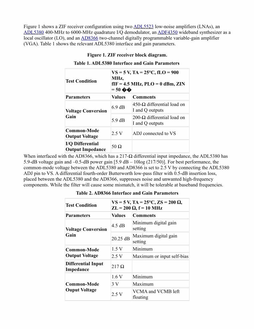
Figure 1 shows a ZIF receiver configuration using two ADL5523 low-noise amplifiers (LNAs), an ADL5380 400-MHz to 6000-MHz quadrature I/Q demodulator, an ADF4350 wideband synthesizer as a local oscillator (LO), and an AD8366 two-channel digitally programmable variable-gain amplifier (VGA). Table 1 shows the relevant ADL5380 interface and gain parameters.
Figure 1. ZIF receiver block diagram.
Table 1. ADL5380 Interface and Gain Parameters
Test Condition
VS = 5 V, TA = 25°C, fLO = 900 MHz,fIF = 4.5 MHz, PLO = 0 dBm, ZIN = 50
Parameters Values Comments
Voltage Conversion Gain
6.9 dB 450-Ω differential load on I and Q outputs
5.9 dB 200-Ω differential load on I and Q outputs
Common-Mode Output Voltage 2.5 V ADJ connected to VS
I/Q Differential Output Impedance 50 Ω
When interfaced with the AD8366, which has a 217-Ω differential input impedance, the ADL5380 has 5.9-dB voltage gain and –0.5-dB power gain [5.9 dB – 10log (217/50)]. For best performance, the common-mode voltage between the ADL5380 and AD8366 is set to 2.5 V by connecting the ADL5380 ADJ pin to VS. A differential fourth-order Butterworth low-pass filter with 0.5-dB insertion loss, placed between the ADL5380 and the AD8366, suppresses noise and unwanted high-frequency components. While the filter will cause some mismatch, it will be tolerable at baseband frequencies.
Table 2. AD8366 Interface and Gain Parameters
Test Condition VS = 5 V, TA = 25°C, ZS = 200 Ω,ZL = 200 Ω, f = 10 MHz
Parameters Values Comments
Voltage Conversion Gain
4.5 dB Minimum digital gain setting
20.25 dB Maximum digital gain setting
Common-Mode Output Voltage
1.5 V Minimum2.5 V Maximum or input self-bias
Differential Input Impedance 217 Ω
Common-Mode Ouput Voltage
1.6 V Minimum3 V Maximum
2.5 V VCMA and VCMB left floating
Differential Output Impedance 28 Ω
Linear Output Swing 6 V p-p 1-dB gain compression
The common-mode output voltage of the AD8366 can be set to 2.5 V; it has best linearity when VCM is left floating. Unfortunately, the AD6642 has best performance with 0.9-V common-mode input voltage (0.5 × AVDD). Because the common-mode output voltage of the AD8366 must be between 1.6 V and 3 V, the AD6642 VCM and AD8366 VCM terminals cannot be connected directly, and resistors must be used to divide the AD8366 common-mode output voltage down to 0.9 V.
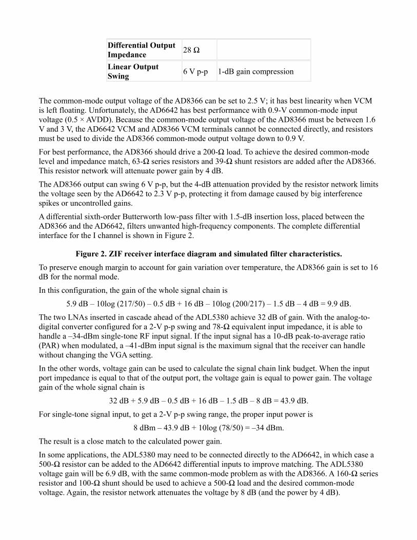
For best performance, the AD8366 should drive a 200-Ω load. To achieve the desired common-mode level and impedance match, 63-Ω series resistors and 39-Ω shunt resistors are added after the AD8366. This resistor network will attenuate power gain by 4 dB.
The AD8366 output can swing 6 V p-p, but the 4-dB attenuation provided by the resistor network limits the voltage seen by the AD6642 to 2.3 V p-p, protecting it from damage caused by big interference spikes or uncontrolled gains.
A differential sixth-order Butterworth low-pass filter with 1.5-dB insertion loss, placed between the AD8366 and the AD6642, filters unwanted high-frequency components. The complete differential interface for the I channel is shown in Figure 2.
Figure 2. ZIF receiver interface diagram and simulated filter characteristics.
To preserve enough margin to account for gain variation over temperature, the AD8366 gain is set to 16 dB for the normal mode.
In this configuration, the gain of the whole signal chain is
5.9 dB – 10log (217/50) – 0.5 dB + 16 dB – 10log (200/217) – 1.5 dB – 4 dB = 9.9 dB.
The two LNAs inserted in cascade ahead of the ADL5380 achieve 32 dB of gain. With the analog-to-digital converter configured for a 2-V p-p swing and 78-Ω equivalent input impedance, it is able to handle a –34-dBm single-tone RF input signal. If the input signal has a 10-dB peak-to-average ratio (PAR) when modulated, a –41-dBm input signal is the maximum signal that the receiver can handle without changing the VGA setting.
In the other words, voltage gain can be used to calculate the signal chain link budget. When the input port impedance is equal to that of the output port, the voltage gain is equal to power gain. The voltage gain of the whole signal chain is
32 dB + 5.9 dB – 0.5 dB + 16 dB – 1.5 dB – 8 dB = 43.9 dB.
For single-tone signal input, to get a 2-V p-p swing range, the proper input power is
8 dBm – 43.9 dB + 10log (78/50) = –34 dBm.
The result is a close match to the calculated power gain.
In some applications, the ADL5380 may need to be connected directly to the AD6642, in which case a 500-Ω resistor can be added to the AD6642 differential inputs to improve matching. The ADL5380 voltage gain will be 6.9 dB, with the same common-mode problem as with the AD8366. A 160-Ω series resistor and 100-Ω shunt should be used to achieve a 500-Ω load and the desired common-mode voltage. Again, the resistor network attenuates the voltage by 8 dB (and the power by 4 dB).
A low-pass filter with 1.5-dB insertion loss, placed between the ADL5380 and AD6642, filters unwanted frequency components. The input impedance is 50 Ω, and the output impedance is 500 Ω. In this configuration, the gain of the whole signal chain is
6.9 dB – 10log (500/50) – 1.5 dB – 4 dB = –8.6 dB.
Superheterodyne Receiver Interface Design and Gain CalculationIn superheterodyne receivers, the system uses ac coupling, so the dc common-mode voltage does not have to be considered when interfacing these circuits.
Many mixers, such as the ADL535x and ADL580x, have 200-Ω differential output impedance, so the power gain and voltage gain are presented separately for different output impedances.
Figure 3 shows one channel of a superheterodyne receiver implemented with an ADL5523 low-noise amplifier; an ADL5356 dual balanced mixer with LO buffer, IF amplifier, and RF balun; a low-pass filter; an AD8376 dual ultralow distortion IF VGA; another low-pass filter; and an AD6642 dual IF receiver.
Figure 3. Superheterodyne receiver diagram; one channel shown.
This design uses a 140-MHz IF and 20-MHz bandwidth, so the parts can be ac-coupled.
The AD5356 has best performance with a 200-Ω load, but the AD8376 has 150-Ω input impedance. Thus, to suppress mixer output spurs and provide better impedance matching, the differential LC filter must have 200-Ω input impedance and 150-Ω output impedance. In applications where the output band signal must be suppressed by a sharp filter, a differential SAW filter can be used, but this introduces loss and group delay in the receiver signal chain. A differential fourth-order band-pass Butterworth filter may be suitable for many wireless receivers because the RF filter can provide enough attenuation for out-of-band interference.
Table 3. ADL5356 and AD8376 Interface and Gain Parameters
ADL5356 Test Condition
VS = 5 V, TA = 25°C, fRF = 1900 MHz,fLO = 1760 MHz, LO power = 0 dBm
Parameters Values Comments
Voltage Conversion Gain 14.5 dB
ZSOURCE = 50 Ω, differentialZLOAD = 200 Ω differential
Power Conversion Gain 8.2 dB Including 4:1 IF port
transformer and PCB loss
AD8376 Test Condition
VS = 5 V, TA = 25°C, RS = RL = 150 Ω at 140 MHz
Parameters Values CommentsDifferential Input Resistance 150 Ω
Voltage Conversion Gain
–4 dB Minimum digital setting20 dB Maximum digital setting
Output Impedance 16 kΩ || 0.8 pF
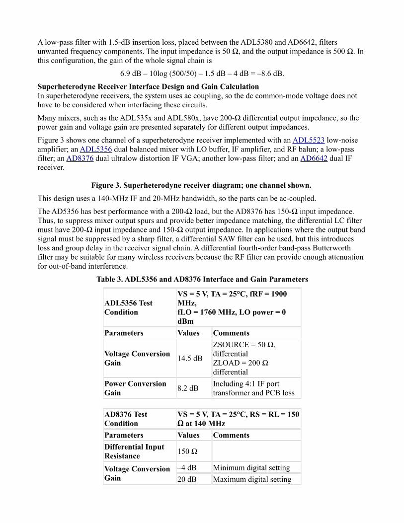
The AD8376’s current-output circuit has high output impedance, so 150-Ω is needed between its differential outputs. Another differential filter must attenuate the second- and third-harmonic distortion components, so this 150-Ω load is divided into two parts. First, a 300-Ω resistor is installed in the output of the AD8376. Another 300-Ω resistor is formed by two 165-Ω resistors and the ADC’s 3-kΩ input impedance. The two 165-Ω resistors also provide the dc common-mode voltage for the ADC input. The LC filter’s input and output impedances are both 300 Ω. Perfect source and load matching is very important for high-IF applications. The complete interface is shown in Figure 4.
Figure 4. Superheterodyne receiver interface diagram and filter simulation result.
In the receiver, a 20-dB LNA is installed ahead of the mixer. The filter after the mixer has 2-dB insertion loss; the filter between the AD8376 and the ADC has 1.2-dB insertion loss. The AD8376 gain is set to 14 dB to provide enough margin to account for temperature variation. The overall gain of the receiver is
20 dB + 8.2 dB – 2 dB + 14 dB – 1.2 dB = 39 dB.
To limit the ADC input voltage to less than 2 V p-p, the power transmitted to the 150-Ω resistance (300 Ω || (165 Ω × 2) || 3 k Ω) should be smaller than 5.2 dBm. The maximum input power for the receiver is thus –33.8 dBm for a single-tone signal. If the input signal is a 10-dB PAR modulation signal, the maximum input signal using this gain setting is –40.8 dBm.
Transmitter Interface Design and Gain CalculationFor Tx-channel designs, both ZIF and superheterodyne architectures have similar interface characteristics, and both need dc coupling between the TxDAC® and the modulator. Most modulators’ IF input circuits should be biased by a dc voltage externally; the TxDAC output can provide dc bias for the modulator in a dc-coupled mode. Most high-speed DACs have current outputs, so an output resistor is needed to produce an output voltage for the modulator.
Figure 5 shows a superheterodyne or ZIF transmitter implemented with an AD9122 TxDAC, a low-pass filter, an ADL537x quadrature modulator, another RF filter, an ADF4350 synthesizer, an ADL5243 digitally controlled VGA, a power amplifier, and an AD562x DAC to control the power amplifier’s (PA) gate voltage.
Figure 5. Transmitter diagram.
For the AD9122, the full-scale output current can be set between 8.66 mA and 31.66 mA. For full-scale currents greater than 20 mA, the spurious-free dynamic range (SFDR) is decreased, but the output power and ACPR of the DAC decrease with lower full-scale current settings. A suitable compromise is a 0-mA to 20-mA current output consisting of a 20-mA ac current riding on a 10-mA dc level.
Table 4. AD9122 and ADL5372 Interface and Gain Parameters
AD9122 Test Condition
AVDD33 = 3.3 V, DVDD33 = 3.3 V, DVDD18 = 1.8 V, CVDD18 = 1.8 V
Parameters Values CommentsFull-Scale Output Current
8.66 mA Minimum digital full scale setting
31.66 mA Maximum digital full scale setting
Output Resistance 10 MΩ
ADL5372 Test Condition
VS = 5 V, TA = 25°C, fLO = 1900 MHz,fIF = 140 MHz
Parameters Values Comments
Output Power 7.1 dBm VIQ = 1.4 V p-p differential
I and Q Input Bias Level 0.5 V Recommended
Differential Input Impedance 2900 kΩ
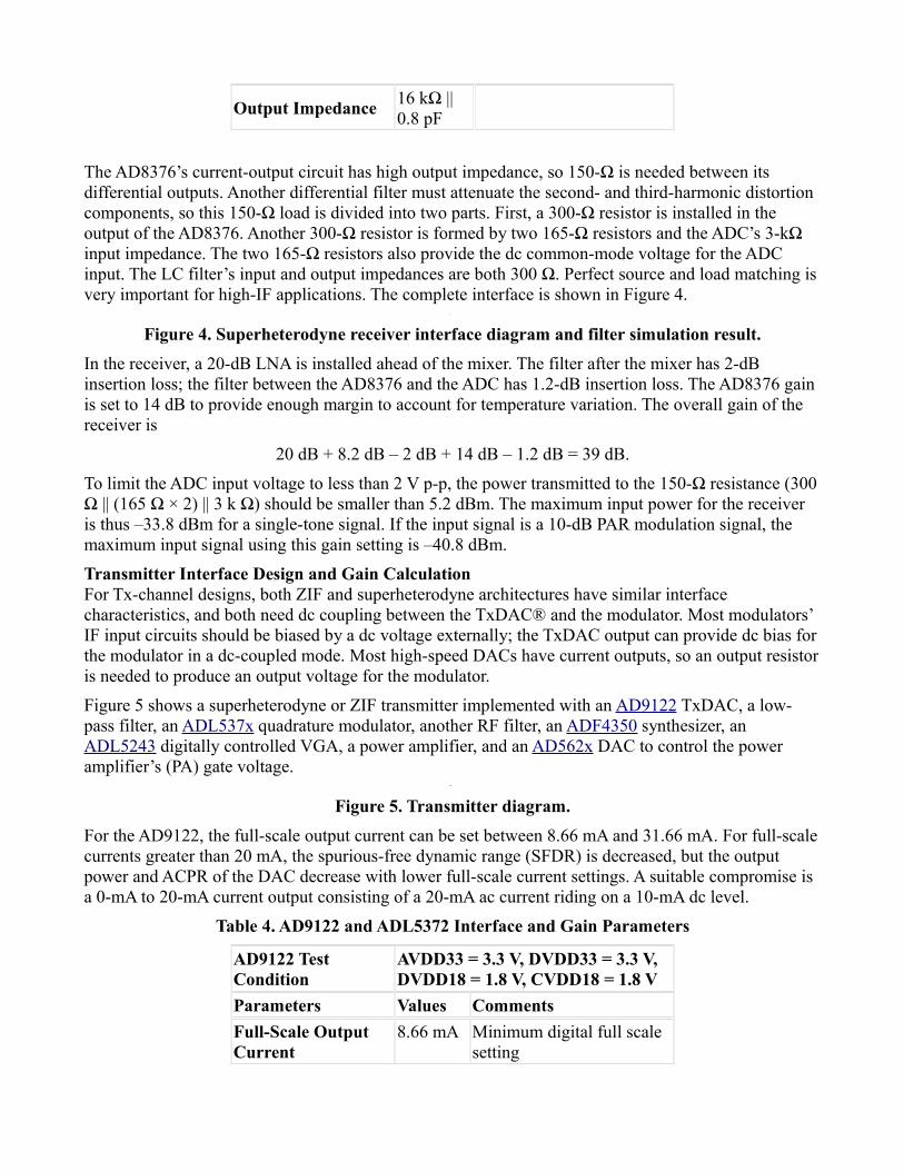
The input circuit of the ADL5372 needs a 0.5-V common-mode voltage, which is provided by a 10-mA dc current flowing through a 50-Ω resistor. The 0-mA to 20-mA ac current is shared by two 50-Ω resistors and a 100-Ω resistor. The ac voltage between the modulator inputs is thus 20 mA × ((50 × 2) || 100) = 1 V p-p. The filter between the TxDAC and the modulator removes unwanted frequency components. The input and output impedance of the filter is 100 Ω. The complete interface is shown in Figure 6.
Figure 6. DC coupled transmitter IF interface diagram and filter simulation result.
With a 50-Ω output, the voltage conversion gain of the ADL5372 is 0.2 dBm. With a 13-dB PAR modulator signal, the average power must be reduced by at least 15 dB for the Tx digital predistortion process. With a 1-V p-p single-tone input to the ADL5372, the average modulator output power is 7.1 dBm – 2.9 dBm = 4.2 dBm. If the 2.2-dBm insertion loss of the low-pass filter is considered, the peak output power is 4.2 dBm – 2.2 dBm = 2 dBm. In this state, an average output power of –10 dBm is presented at the output of the modulator.
With an 11-dBm average power signal, a PA-driver with 26-dBm P1dB is needed in the Tx signal chain. If a 2-dB insertion-loss RF filter is needed to suppress LO feedthrough and sideband output of the modulator, then the gain block and PA driver have to provide a total of 21-dB gain. The ADL5243 VGA with integrated gain block, digitally controlled attenuator, and PA driver is suggested for this application.
ConclusionThis paper describes ZIF and superheterodyne receiver differential interfaces for the demodulator, IF VGA, mixer, and analog port of the ADC, as well as transmitter differential interfaces between the TxDAC and FMOD, using Analog Devices parts for active portions of the signal chain. Gain calculations and simulation results are presented for the application filters that were designed for these circuits. Additional information can be found in the following references.
ReferencesCircuit Note CN-0018, Interfacing the ADL5372 I/Q Modulator to the AD9779A Dual-Channel, 1 GSPS High-Speed DAC.
Circuit Note CN-0134, Broadband Low Error Vector Magnitude (EVM) Direct Conversion Transmitter.

Calvo, Carlos. “The differential-signal advantage for communications system design.” EE Times.
Author
Mingming Zhao [[email protected]] is a field applications engineer for ADI North China in Beijing, China. Mingming mainly supports RF and high-speed converter product applications. After earning a master’s degree in electromagnetic and microwave technology from the Chinese Academy of Sciences, and spending more than two years as an RF engineer at Datang Mobile Telecommunication Equipment Co, Ltd., Mingming joined Analog Devices in 2010.
Insight into digiPOT Specifications and Architecture Enhances AC Performance
By Miguel Usach Merino
Digital potentiometers (digiPOTs) provide a convenient way to adjust the ac or dc voltage or current output of sensors, power supplies, or other devices that require some type of calibration—with timing, frequency, contrast, brightness, gain, and offset adjustment being just a few of the possibilities. Digital setting avoids virtually all of the problems associated with mechanical potentiometers, such as physical size, mechanical wear out, wiper contamination, resistance drift, and sensitivity to vibration, temperature, and humidity—and eliminates layout inflexibility resulting from the need for screwdriver access.
The digiPOT can be used in two different modes: potentiometer or rheostat. In potentiometer mode, shown in Figure 1, three terminals are available; the signal is connected across Terminals A and B, while Terminal W (as in wiper) provides the attenuated output voltage. When the digital ratio-control input is all zeros, the wiper is typically connected to Terminal B.
Figure 1. Potentiometer mode.
When the wiper is hardwired to either end, the potentiometer becomes a simple variable resistor, or rheostat, as shown in Figure 2. The rheostat mode permits a smaller form factor, since fewer external pins are required. Some digiPOTs are available only as rheostats.
Figure 2. Rheostat mode.
There are no restrictions on the polarity of currents or voltages appearing at the digiPOT resistance terminals, but the amplitude of ac signals cannot exceed the power-supply rails (VDD and VSS)—and the maximum current, or current density, should be limited when the part is operated in rheostat mode, especially at lower resistance settings.
Typical ApplicationsSignal attenuation is inherent in potentiometer mode, for the device is basically a voltage divider. The output signal is defined as: VOUT = VIN × (RDAC/RPOT), where RPOT is the nominal end-to-end resistance of the digiPOT, and RDAC is the digitally selected resistance between W and the reference pin of the input signal, typically Terminal B, as shown in Figure 3.
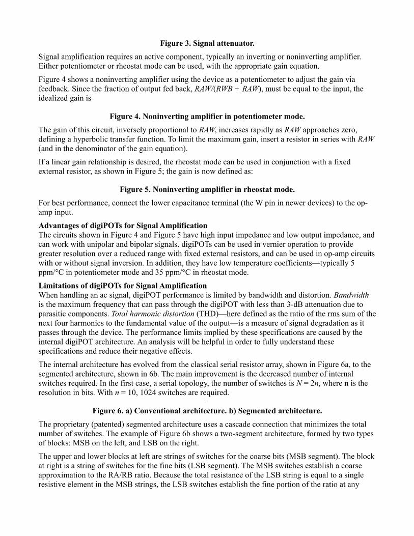
Figure 3. Signal attenuator.Signal amplification requires an active component, typically an inverting or noninverting amplifier. Either potentiometer or rheostat mode can be used, with the appropriate gain equation.
Figure 4 shows a noninverting amplifier using the device as a potentiometer to adjust the gain via feedback. Since the fraction of output fed back, RAW/(RWB + RAW), must be equal to the input, the idealized gain is
Figure 4. Noninverting amplifier in potentiometer mode.
The gain of this circuit, inversely proportional to RAW, increases rapidly as RAW approaches zero, defining a hyperbolic transfer function. To limit the maximum gain, insert a resistor in series with RAW (and in the denominator of the gain equation).
If a linear gain relationship is desired, the rheostat mode can be used in conjunction with a fixed external resistor, as shown in Figure 5; the gain is now defined as:
Figure 5. Noninverting amplifier in rheostat mode.
For best performance, connect the lower capacitance terminal (the W pin in newer devices) to the op-amp input.
Advantages of digiPOTs for Signal AmplificationThe circuits shown in Figure 4 and Figure 5 have high input impedance and low output impedance, and can work with unipolar and bipolar signals. digiPOTs can be used in vernier operation to provide greater resolution over a reduced range with fixed external resistors, and can be used in op-amp circuits with or without signal inversion. In addition, they have low temperature coefficients—typically 5 ppm/°C in potentiometer mode and 35 ppm/°C in rheostat mode.
Limitations of digiPOTs for Signal AmplificationWhen handling an ac signal, digiPOT performance is limited by bandwidth and distortion. Bandwidth is the maximum frequency that can pass through the digiPOT with less than 3-dB attenuation due to parasitic components. Total harmonic distortion (THD)—here defined as the ratio of the rms sum of the next four harmonics to the fundamental value of the output—is a measure of signal degradation as it passes through the device. The performance limits implied by these specifications are caused by the internal digiPOT architecture. An analysis will be helpful in order to fully understand these specifications and reduce their negative effects.
The internal architecture has evolved from the classical serial resistor array, shown in Figure 6a, to the segmented architecture, shown in 6b. The main improvement is the decreased number of internal switches required. In the first case, a serial topology, the number of switches is N = 2n, where n is the resolution in bits. With n = 10, 1024 switches are required.
Figure 6. a) Conventional architecture. b) Segmented architecture.
The proprietary (patented) segmented architecture uses a cascade connection that minimizes the total number of switches. The example of Figure 6b shows a two-segment architecture, formed by two types of blocks: MSB on the left, and LSB on the right.
The upper and lower blocks at left are strings of switches for the coarse bits (MSB segment). The block at right is a string of switches for the fine bits (LSB segment). The MSB switches establish a coarse approximation to the RA/RB ratio. Because the total resistance of the LSB string is equal to a single resistive element in the MSB strings, the LSB switches establish the fine portion of the ratio at any

point of the main string. The A and B MSB switches are complementary coded.
The number of switches in the segmented architecture is:
N = 2m + 1 + 2n – m,
where n is the total number of bits and m the number of bits of resolution in the MSB word. For example, if n = 10 and m = 5, 96 switches are required.
The segmented scheme requires fewer switches than the conventional string:
Difference = 2n – (2m + 1 + 2n – m)
In this example, the savings would be
1024 – 96 = 928!
In both architectures, switches are responsible for choosing among the different resistance values, making it important to understand the ac error sources in an analog switch. These CMOS (complementary-metal-oxide semiconductor) switches are made up of P-channel and N-channel MOSFETs in parallel. This basic bilateral switch maintains a fairly constant resistance (RON) for signals up to the full supply rails.
BandwidthFigure 7 shows the parasitic components that affect the ac performance of CMOS switches.
Figure 7. CMOS switch model.
CDS = drain-source capacitance; CD = drain-gate + drain-bulk capacitance; CS = source-gate + source-bulk capacitance.
The transfer relationship is defined in the equation below, where these assumptions have been applied:
• Source impedance is 0 Ω • No external load contribution • No contribution from CDS • RLSB << RMSB
where:
RDAC is the resistance setting
RPOT is the end-to-end resistance
CDLSB is the total drain-gate + drain-bulk capacitance in the LSB segment
CSLSB is the total source-gate + source-bulk capacitance in the LSB segment
CDMSB is the drain-gate + drain-bulk capacitance in the MSB switch
CSMSB is the source-gate + source-bulk capacitance in the MSB switch
moff is the number of off switches in the signal MSB path
mon is the number of on switches in the signal MSB path
The transfer equation has many factors and is somewhat code-dependent, so the following further assumptions are used to simplify the equation
CDMSB + CSMSB = CDSMSBCDLSB + CSLSB >> CDSMSB
(CDLSB + CSLSB) = CW (specified in the data sheet)
The CDS contribution adds a zero in the transfer equation, but since this occurs typically at much higher frequency than the pole, an RC low-pass filter is the dominant response. A good approximation of the simplified equati on is:
and the bandwidth (BW) is defined as:
where CL is the load capacitance.
The BW is code dependent, and the worst case is when the code is at half scale, a digital value of 29 = 512 for the AD5292 and 27 = 128 for the AD5291 (see Appendix). Figure 8 shows the low-pass filtering effect as a function of code for various nominal resistance and load capacitance values.
Figure 8. Maximum bandwidth vs. load capacitance for various resistance values.
The parasitic track capacitance of the PC board should be taken into account, otherwise the maximum BW will be lower than expected; the track capacitance can be calculated straightforwardly as
where
εR is the dielectric constant of the board material
A is the track area (cm2)
d is the distance between layers (cm)
For example, assuming FR4 board material with two signal layers and power/ground planes, εR = 4, track length = 3 cm, width = 1.2 mm, and distance between layers = 0.3 mm; the total track capacitance is about 4 pF.
DistortionThe THD is used to quantify the nonlinearity of the device as an attenuator. This nonlinearity is due to the internal switches and their RON variation with voltage. An exaggerated example of amplitude distortion is shown in Figure 9.
Figure 9. Distortion.
The RON of a switch is quite small when compared with the resistance of a single internal passive resistor, and its variation over the signal range is even smaller. Figure 10 shows a typical on-resistance characteristic.
Figure 10. CMOS resistance.
The resistance curve does depend on the supply voltage rails; the internal switches have the lowest RON variation at maximum supply voltage. If the supply voltage is decreased, the RON variation, and hence the nonlinearity, increases. Figure 11 compares RON variation at two supply levels for a low-voltage digiPOT.
Figure 11. Switch resistance variation vs. supply voltage.
The THD depends on multiple factors and is thus hard to quantify, but assuming a 10% variation in RON, the following equation can be used as a rough approximation:
As a general rule, the higher the nominal digiPOT resistance (RPOT), the better the THD, as the
denominator is larger.
Trade-OffsDistortion and bandwidth both decrease with increased RPOT, so it is not possible to improve one specification without penalizing the other. So the circuit designer must choose an appropriate balance. This is also true at the device design level, since the IC designer must balance the parameters in the design equations:
where
COX is the oxide capacitance
μ is the mobility constant of the electron (NMOS) or hole (PMOS)
W is the width
L is the length
BiasingFrom the practical point of view one must make the best of these specifications. When the digiPOT is used to attenuate an ac signal with capacitive coupling, the lowest distortion is achieved if the signal is biased to the mid-value of the power supply. This means that the switches are working on the most linear portion of the resistance characteristic.
One approach is to use a dual supply and simply ground the potentiometer to the power-supply common. The signal can then have a positive-negative swing. Another way, if a single supply is required, or the particular digiPOT doesn’t support dual supply, is to add an offset voltage of VDD/2 to the ac signal. This offset voltage must be added at both resistor terminals, as shown in Figure 12.
Figure 12. Single-supply ac signal conditioning.
If a signal amplifier is required, an inverting amplifier, with a dual supply, as shown in Figure 13, is preferred over the noninverting amplifier for two reasons:
• Provides better THD performance because the virtual ground at the inverting pin will center the switch resistance in the middle of the voltage range.
• As the inverting pin is at virtual ground, the wiper capacitance, CDLSB, is almost canceled to obtain a small increase in bandwidth (but one must pay attention to circuit stability).
Figure 13. Adjustable amplification using a digiPOT with an inverting amplifier.
APPENDIX—ABOUT THE AD5291/AD5292256-/1024-Position Digital Potentiometers Are 1% Accurate, 20-Time ProgrammableThe AD5291/AD5292 digital potentiometers, shown in Figure 14, feature 256-/1024-position resolution. End-to-end resistance options of 20 kΩ, 50 kΩ, and 100 kΩ are available, with better than 1% tolerance—and temperature coefficients of 35 ppm/°C in rheostat mode and 5 ppm/°C (ratio) in divider mode. The devices perform the same electronic adjustment function as mechanical potentiometers, but are smaller and more reliable. Their wiper position can be adjusted via an SPI-compatible interface. Unlimited adjustments can be made before blowing a fuse to fix the wiper position, a process analogous to putting epoxy on a mechanical trimmer. This process can be repeated up to 20 times (“removing the epoxy”). Operating on a single 9-V to 33-V supply or dual ±9-V to ±16.5-V supplies, the AD5291/AD5292 dissipate 8 μW. Available in 14-lead TSSOP packages, they are specified from –40°C to +105°C. (return to text)
Figure 14. AD5291/AD5292 functional block diagram.
Author
Miguel Usach Merino [[email protected]] received his degree in electronic engineering from Universitat de Valencia. Miguel joined ADI in 2008 and works as an applications engineer in the Precision DAC Group in Limerick, Ireland.
Power Management Design for PLLs
By Austin Harney and Grzegorz Wawrzola
AbstractThe phase-locked loop (PLL) is a fundamental building block of modern communication systems. PLLs are typically used to provide the local-oscillator (LO) function in a radio receiver or transmitter; they are also used for clock-signal distribution and noise reduction—and, increasingly, as the clock source for high-sampling-rate analog-to-digital or digital-to-analog conversion.
As the noise performance of PLLs is improving with each generation, the impact of power supply noise is becoming increasingly evident, and can even limit noise performance in some cases.
This article considers the basic PLL scheme shown in Figure 1 and examines the power-management requirements for each building block.
Figure 1. A basic phase-locked loop showing the various power-management requirements.
In a PLL, the feedback control loop drives a voltage-controlled oscillator (VCO) to make the oscillator frequency (or phase) accurately track a multiple of an applied reference frequency. Many good references, for example, Best’s Phase-Locked Loops,1 explain the mathematical analysis of the PLL; and simulation tools, such as Analog Devices’ ADIsimPLL™, can be helpful in understanding the loop transfer functions and calculations. Let us now look at the PLL building blocks in turn.
The VCO and VCO PushingThe voltage-controlled oscillator converts the error voltage from the phase detector into an output frequency. Its “gain,” defined as KVCO, is usually specified in MHz/V. A voltage-controlled variable-capacitance diode (varactor) is often used to adjust frequency in VCOs. The gain of the VCO is usually large enough to provide adequate frequency coverage, but not so large as to degrade phase noise—since any varactor noise will be amplified by KVCO and contribute to output phase noise.
The advent of multiband integrated VCOs, such as that used in the ADF4350 frequency synthesizer with integrated VCO, obviates the trade-off between KVCO and frequency coverage, allowing the PLL designer to use an IC containing several moderate-gain VCOs, with intelligent band switching routines to select the appropriate band, depending on the programmed output frequency. This partitioning of the frequency band provides wide overall range and lower noise.
In addition to the desired translation from input voltage change to output frequency change (KVCO), power-supply variation can produce an unwanted component of output frequency change. The sensitivity of the VCO to power-supply variation is defined as the VCO pushing (Kpushing), usually a fraction of the wanted KVCO. For example, Kpushing is usually 5% to 20% of KVCO. Thus, for high-gain VCOs, the pushing effect becomes larger, and the noise contribution from the VCO supply source becomes more critical.
VCO pushing is measured by applying a dc tuning voltage to the VTUNE pin, varying the power supply voltage, and measuring the frequency change. The pushing figure is the ratio of frequency change to voltage change, as shown in Table 1, using the ADF4350 PLL.
Table 1. ADF4350 VCO Pushing Measurements
VCO Band (MHz
Vtune(V)
f1 (MHz) at VVCO = 3 V
f2 (MHz) at VVCO = 3.3 V
Kpushing = Δf/ΔV (MHz/V)
)
2200 2.5 2233.446 2233.061 1.28
3300 2.5 3331.112 3331.799 2.3
4400 2.5 4462.577 4464.242 5.55
Another method, mentioned in Reference 2, is to dc-couple a low-frequency square wave into the supply, while observing the frequency-shift-keyed (FSK) modulation peaks on either side of the VCO spectrum (Figure 2). The frequency deviation between the peaks divided by the amplitude of the square wave yields the VCO pushing number. This can be a more accurate measure than the static dc test, as it removes any thermal effects associated with a change in dc input voltage. Figure 2 shows a spectrum analyzer plot of the ADF4350 VCO output at 3.3 GHz with a 10 kHz, 0.6 V p-p square wave applied to the nominal 3.3-V supply. The resulting deviation is 3326.51 MHz – 3324.89 MHz = 1.62 MHz, for a pushing number of 1.62 MHz/0.6 V or 2.7 MHz/V. This compares to the static measure of 2.3 MHz/V given in Table 1.
Figure 2. A spectrum-analyzer plot of ADF4350 VCO response to supply modulation by a 10-kHz,
0.6-V p-p square wave.In a PLL system, higher VCO pushing means greater multiplication of VCO power-supply noise. A low-noise power supply is required to minimize the impact on VCO phase noise.
Reference 3 and Reference 4 provide good examples of how different low-dropout regulators (LDOs) can affect PLL phase-noise. For example, a comparison was made between the ADP3334 and ADP150 LDOs in powering an ADF4350. The integrated rms noise of the ADP3334 regulator is 27 µV (over four decades, from 10 Hz to 100 kHz). This compares to 9 µV for the ADP150, the LDO used on the ADF4350 evaluation board. The difference in measured PLL phase-noise spectral density can be seen in Figure 3. The measurement was taken with a 4.4-GHz VCO frequency, where the VCO pushing was maximum (Table 1), so this is a worst-case result. The ADP150 regulator noise was low enough so that its contribution did not measurably add to the VCO noise, as was confirmed by repeating the measurement with two (presumably “noiseless”) AA batteries.
Figure 3. ADF4350 phase noise comparison at 4.4 GHz when powered with pairs of ADP3334 and
ADP150 LDOs—and AA batteries.Figure 3 emphasizes the importance of a low-noise power source for the ADF4350, but how do you specify the noise requirement of the power supply or LDO?
In a manner similar to VCO noise, the phase noise contribution of the LDO can be modeled as an additive component, ΦLDO(t), as shown in Figure 4. Reusing the VCO excess phase expression yields:
or, in the frequency domain
where vLDO(f) is the voltage noise spectral density of the LDO.
The single-sideband power spectral density SΦ(f) in a 1-Hz bandwidth is given by
Expressing this in dB, the formula for calculating the phase noise contribution due to the power supply
noise is: (1)
where L(LDO) is the noise contribution from the regulator to the VCO phase noise (in dBc/Hz), at an offset f; Kpushing is the VCO pushing figure in Hz/V; and vLDO(f) is the noise spectral density at a given frequency offset in V/√Hz.
Figure 4. Small-signal additive VCO supply noise model.
In a free-running VCO, the total noise is the root-sum-square (rss) of LLDO and the VCO noise. Thus, expressed in dB:
For example, consider a VCO with a pushing number of 10 MHz/V and a measured phase noise of –116 dBc/Hz at 100 kHz offset: what is the required noise spectral density of the power supply so as to not degrade the VCO noise performance at 100 kHz? The supply noise and VCO noise add as the root-sum-square, so the supply noise should be at least 6 dB less than the VCO noise to minimize its contribution. Thus, LLDO should be less than –122 dBc/Hz. Using Equation 1,
solving for vLDO(f),
vLDO(f) = 11.2 nV/√Hz at 100-kHz offset
The LDO noise spectral density at a given offset can usually be read from the LDO data sheet’s typical performance curves.
When the VCO is connected in a negative-feedback PLL, the LDO noise, LLDO, is high-pass filtered by the PLL loop filter, in a similar manner to VCO noise. Thus, the above formula only applies to frequency offsets greater than the PLL loop bandwidth. Within the PLL’s loop bandwidth, the PLL can successfully track and filter the LDO noise, reducing its contribution.
LDO FilteringTo improve LDO noise, there are typically two choices: use an LDO with less noise or post-filter the LDO’s output. The filtering option can be a good choice when the noise requirements without a filter are beyond the capability of affordable LDOs. A simple LC π-filter is often sufficient to reduce out-of-band LDO noise by 20 dB (Figure 5).
Figure 5. LC π-filter to attenuate LDO noise.
Care is needed in the choice of components. A typical inductor will be in the microhenry range—with a ferrite core—so it is necessary to consider its saturation current (ISAT), specified in inductor data sheets as the dc current level at which the inductance drops by 10%. The current drawn by the VCO should be less than ISAT. Effective series resistance(ESR) is also a concern, as this will cause an IR drop across the filter. For a microwave VCO drawing 300-mA dc, an inductor with ESR less than 0.33 Ω would be needed to yield an IR drop of less than 100 mV. A low, but nonzero, ESR is also desirable to damp the filter response and improve LDO stability. It can be practical to choose a capacitor with very low parasitic ESR and add a dedicated series resistor for this purpose. This can all be simulated easily in SPICE using a downloadable component evaluator such as NI Multisim™.
Charge Pump and FilterThe charge pump converts the phase detector error voltage into current pulses, which are integrated and smoothed by the PLL loop filter. The charge pump can typically operate at up to 0.5 V below its supply voltage (VP). For example, if the maximum charge pump supply is 5.5 V, the charge pump could only
operate at an output voltage up to 5 V. If the VCO requires higher tuning voltages, an active filter is typically required. Useful information and a reference design of an actual PLL can be found in Circuit Note CN-0174,5 and ways of dealing with high-voltage are discussed in “Designing High-Performance Phase-Locked Loops with High-Voltage VCOs,”6 which appeared in Analog Dialogue Volume 43, Number 4 (2009). The alternative to an active filter is to use a PLL with a charge pump designed for higher voltage, such as the ADF4150HV. The ADF4150HV can operate with charge-pump voltages as high as 30 V, thus avoiding the need for active filters in many cases.
The low current drawn by the charge pump makes it look attractive to use a boost converter to generate the high charge-pump voltage from a lower supply voltage, but the switching-frequency ripple associated with this type of dc-to-dc converter could produce unwanted spurious tones at the output of the VCO. High PLL spurs can potentially cause failure of a transmitter emission mask test or degrade sensitivity and out-of-band blocking in a receiver system. To help guide the specification of converter ripple, a comprehensive power supply rejection plot vs. frequency was taken for various PLL loop bandwidths, using the measurement setup of Figure 6.
Figure 6. Setup for measuring charge pump power-supply rejection.
A ripple signal of 17.4 mV (–22 dBm) was ac-coupled to the power supply voltage and swept over a frequency range. At each frequency the spurious level was measured and the PSR calculated as the difference in dB between the –22-dBm input and the spurious output level. The 0.1-μF and 1-nF charge pump supply decoupling capacitors, which were left in place, provided some attenuation of the coupled signal, so the signal level at the generator was increased until 17.4 mV was measured directly at the pin at each frequency point. The results are shown in Figure 7.
The power supply rejection gets worse initially as the frequency increases within the PLL loop bandwidth. As the frequency approaches the PLL loop bandwidth, the ripple frequency gets attenuated in a similar manner to reference noise, and PSR improves. This plot shows that a boost converter with higher switching frequency—ideally greater than 1 MHz—is desirable to minimize switching spurs. Also, the PLL loop bandwidth should be minimized wherever possible.
With a switching speed of 1.3 MHz, the ADP1613 is a good example of a suitable boost converter. With the PLL loop bandwidth set to 10 kHz, a PSR of about 90 dB is possible; with a loop bandwidth of 80 kHz, the PSR is 50 dB. Starting with the PLL spurious level requirements, one can work backward to determine the ripple level needed at the boost converter output. For example, if the PLL requires spurs less than –80 dBm, and the PSR is 50 dB, then the ripple power at the input to the charge pump supply needs to be less than –30 dBm, or 20 mV p-p. These levels of ripple voltage can easily be achieved with ripple filters, if sufficient decoupling capacitance is placed close to the charge pump supply pin. For example, a 100-nF decoupling capacitor provides more than 20 dB of ripple attenuation at 1.3 MHz. Care should be taken to use capacitors with the appropriate voltage rating; for example, if the boost converter generates an 18-V supply, use capacitors with a 20-V or higher rating.
Figure 7. ADF4150HV charge pump power-supply rejection plot.
Design of the boost converter and ripple filter is simplified using the ADP161x Excel-based design tool. Figure 8 shows the user inputs for an illustrative 5-V in to 20-V out design. To minimize voltage ripple at the output of the converter stage, the noise filter option was selected, and the VOUT ripple field was set to its minimum. The current drawn by the high-voltage charge pump is 2 mA maximum, so an IOUT of 10 mA was typed in to provide margin. This design was tested with the ADF4150HV evaluation board, using a PLL loop bandwidth of 20 kHz. From Figure 7, a PSR of about 70 dB might be expected. Due to the excellent PSR, this setup showed no evident switching spurs (< –110 dBm) at the VCO output—even when the noise filter was omitted.
Figure 8. ADP1613 boost converter Excel design tool.
As a final experiment, the PSR of the high-voltage charge pump was compared to that of an active filter, the topology most commonly used today to generate high VCO tuning voltages. To make the measurement, an ac signal with an amplitude of 1 V p-p is injected into the charge pump supply (VP) of the ADF4150HV, using a passive loop filter—as in the measurement setup in Figure 6. The same measurement is repeated with an active filter in place of the passive filter of equal bandwidth. The active filter used was type CPA_PPFFBP1, as described in ADIsimPLL (Figure 9).
Figure 9. Screen view of CPA_PPFFBP1 filter design in ADIsimPLL.
Decoupling is the same on the charge pump and op amp supply pins, to provide a fair comparison—10 μF, 10 nF, and 10 pF capacitors in parallel. The measured result is plotted in Figure 10: the high-voltage charge pump has a 40-dB to 45-dB reduction in switching spur level when compared to the active filter. The improved spur levels with the high-voltage charge pump can be partially explained by the smaller loop filter attenuation seen by the active filter, where the injected ripple is after the first pole, in contrast to the passive filter, where the injected ripple is at the input.
Figure 10. Power supply ripple level for active loop filter vs. high-voltage passive filter.
A final note: the third power rail shown in Figure 1—the divider supply, AVDD/DVDD—has less stringent supply requirements compared to the VCO and charge pump supply, as the RF sections of the PLL (AVDD) are typically bipolar ECL logic stages with stable band-gap-referred bias voltages, and so are relatively supply immune. Also, by their nature, the digital CMOS blocks (DVDD) are more immune to power supply noise. Thus, it is advisable to choose a medium performance LDO that meets both the voltage and current requirements for this rail and apply sufficient decoupling close to all power pins; 100 nF in parallel with 10 pF is usually sufficient.
ConclusionThe power-management requirements for the main PLL blocks were discussed, and specifications were derived for the VCO and charge pump supplies. Analog Devices provides multiple design-in support tools for power management and PLL ICs, including reference circuits and solutions, and simulation tools like ADIsimPLL and ADIsimPower. With an understanding of the impact of power supply noise and ripple on PLL performance, designers can work back to derive specifications for power management blocks and achieve PLL designs with the best possible performance.
References1Best, Roland E. Phase Locked Loops: Design, Simulation, and Applications. 6th edition. 2007. McGraw-Hill. ISBN 9780071493758.
2Colin, Dennis. Externally Induced VCO Phase Noise. Micronetics, Inc. Reprint: Microwave Journal. Feb 2002.
3Collins, Ian. Integrated PLLs and VCOs [Part 2]. Radio-Electronics.com. Nov 2010.
4Circuit Note CN-0147, Powering a Fractional-N Voltage-Controlled Oscillator (VCO) with Low Noise LDO Regulators for Reduced Phase Noise. Analog Devices. 2010.
5Circuit Note CN-0174, Low Noise, 12 GHz, Microwave Fractional-N Phase-Locked Loop (PLL) Using an Active Loop Filter and RF Prescaler. Analog Devices. 2010.
6Harney, Austin. “Designing High-Performance Phase-Locked Loops with High-Voltage VCO.” Analog Dialogue, 43-12. 2009.

Authors
Austin Harney[[email protected]] graduated in 1999 with a BEng from University College, Dublin, Ireland, and an MBA from the University of Limerick in 2006. For 12 years he worked in various RF roles at Analog Devices, and is currently an applications engineer for ADI’s PLL and VCO product family.(return to top)
Grzegorz Wawrzola [[email protected]] graduated with honors in 2006 with an MSc in electronics and telecommunications from Wroclaw University of Technology, Wroclaw, Poland. He worked for five years as a design evaluation engineer for PLLs and VCOs in the RF group at Analog Devices before moving to RF applications in August 2011.