from structure to spectra: tight-binding theory of ingaas
TRANSCRIPT

ITP
From Structure to Spectra:Tight-Binding Theory of InGaAs
Quantum Dots
Elias Goldmann, Master of Science


From Structure to Spectra:Tight-Binding Theory of InGaAs
Quantum Dots
Vom Fachbereich Physik und Elektrotechnikder Universitat Bremen
zur Erlangung des akademischen Grades einesDoktors der Naturwissenschaften (Dr. rer. nat)
genehmigte Dissertation
vonElias Goldmann, Master of Science
aus Duisburg
1. Gutachter: Prof. Dr. rer. nat. Frank Jahnke2. Gutachter: Prof. Dr. rer. nat. Gerd Czycholl
Eingereicht am: 25.06.2014Tag des Promotionskolloquiums: 23.07.2014


For Sonja & Nora Marie.

Self-assembled semiconductor quantum dots have raised considerable interest inthe last decades due to a multitude of possible applications ranging from carrier stor-age to light emitters, lasers and future quantum communication devices. Quantumdots offer unique electronic and photonic properties due to the three-dimensionalconfinement of charge carriers and the coupling to a quasi-continuum of wettinglayer and barrier states.
In this work we investigate the electronic structure of InxGa1−xAs quantum dotsembedded in GaAs, considering realistic quantum dot geometries and Indium con-centrations. We utilize a next-neighbour sp3s∗ tight-binding model for the calcu-lation of electronic single-particle energies and wave functions bound in the nano-structure and account for strain arising from lattice mismatch of the constituentmaterials atomistically. With the calculated single-particle wave functions we de-rive Coulomb matrix elements and include them into a configuration interactiontreatment, yielding many-particle states and energies of the interacting many-carriersystem. Also from the tight-binding single-particle wave functions we derive dipoletransition strengths to obtain optical quantum dot emission and absorption spectrawith Fermi’s golden rule. Excitonic fine-structure splittings are obtained, which playan important role for future quantum cryptography and quantum communicationdevices for entanglement swapping or quantum repeating.
For light emission suited for long-range quantum-crypted fiber communicationInAs quantum dots are embedded in an InxGa1−xAs strain-reducing layer, shiftingthe emission wavelength into telecom low-absorption windows. We investigate theinfluence of the strain-reducing layer Indium concentration on the excitonic fine-structure splitting. The fine-structure splitting is found to saturate and, in somecases, even reduce with strain-reducing layer Indium concentration, a result beingcounterintuitively. Our result demonstrates the applicability of InGaAs quantumdots for quantum telecommunication at the desired telecom wavelengths, offeringgood growth controllability.
For the application in lasers, quantum based active media are known to offer su-perior properties to common quantum well lasers such as low threshold currents ortemperature stability. For device design, the knowledge about the saturation beha-viour of optical gain with excitation density is of major importance. In the presentwork we combine quantum-kinetic models for the calculation of the optical gain ofquantum dot active media with our atomistic tight-binding model for the calculationof single-particle energies and wave functions. We investigate the interplay betweenstructural properties of the quantum dots and many-body effects in the optical gainspectra and identify different regimes of saturation behaviour. Either phase-spacefilling dominates the excitation dependence of the optical gain, leading to satura-tion, or excitation-induced dephasing dominates the excitation dependence of theoptical gain, resulting in a negative differential gain.
vi

Contents
1. Introduction 11.1. Quantum dots (QDs) . . . . . . . . . . . . . . . . . . . . . . . . . . . 21.2. Topics . . . . . . . . . . . . . . . . . . . . . . . . . . . . . . . . . . . 61.3. Brief description of content . . . . . . . . . . . . . . . . . . . . . . . . 7
2. Single-particle theory 92.1. Calculation of electronic bulk band structures . . . . . . . . . . . . . 10
2.1.1. The k·p model . . . . . . . . . . . . . . . . . . . . . . . . . . 102.1.2. Empirical pseudopotentials . . . . . . . . . . . . . . . . . . . . 11
2.2. Empirical tight-binding (TB) . . . . . . . . . . . . . . . . . . . . . . 122.2.1. Introduction . . . . . . . . . . . . . . . . . . . . . . . . . . . . 122.2.2. Tight-binding fundamentals . . . . . . . . . . . . . . . . . . . 132.2.3. Two-center approximation . . . . . . . . . . . . . . . . . . . . 162.2.4. Spin-orbit coupling . . . . . . . . . . . . . . . . . . . . . . . . 202.2.5. Strain . . . . . . . . . . . . . . . . . . . . . . . . . . . . . . . 222.2.6. Piezoelectricity . . . . . . . . . . . . . . . . . . . . . . . . . . 27
2.3. Modelling semiconductor nanostructures . . . . . . . . . . . . . . . . 292.3.1. Bulk band structures . . . . . . . . . . . . . . . . . . . . . . . 302.3.2. Quantum wells . . . . . . . . . . . . . . . . . . . . . . . . . . 382.3.3. Quantum dots . . . . . . . . . . . . . . . . . . . . . . . . . . . 46
2.4. Supercell requirements . . . . . . . . . . . . . . . . . . . . . . . . . . 532.5. Diagonalization of large sparse matrices . . . . . . . . . . . . . . . . . 542.6. Benchmarks . . . . . . . . . . . . . . . . . . . . . . . . . . . . . . . . 552.7. Geometry and single-particle properties . . . . . . . . . . . . . . . . . 572.8. Choice of valence band offset . . . . . . . . . . . . . . . . . . . . . . . 662.9. Number of bound states . . . . . . . . . . . . . . . . . . . . . . . . . 68
3. Many-particle theory 713.1. Full Configuration Interaction . . . . . . . . . . . . . . . . . . . . . . 73
3.1.1. Coulomb matrix elements from TB wave functions . . . . . . . 763.1.2. Many-particle states . . . . . . . . . . . . . . . . . . . . . . . 783.1.3. Dipole matrix elements from TB wave functions . . . . . . . . 793.1.4. Excitonic spectrum . . . . . . . . . . . . . . . . . . . . . . . . 84
3.2. Excitonic fine-structure splitting . . . . . . . . . . . . . . . . . . . . . 86

Contents Contents
4. QDs in single-photon emitters and laser devices 914.1. Evolution of FSS under SRL influence . . . . . . . . . . . . . . . . . 93
4.1.1. Introduction . . . . . . . . . . . . . . . . . . . . . . . . . . . . 934.1.2. System . . . . . . . . . . . . . . . . . . . . . . . . . . . . . . . 944.1.3. Results and discussion . . . . . . . . . . . . . . . . . . . . . . 95
4.2. Optical gain in QD active media . . . . . . . . . . . . . . . . . . . . . 994.2.1. Optical gain . . . . . . . . . . . . . . . . . . . . . . . . . . . . 994.2.2. Envelope approximation . . . . . . . . . . . . . . . . . . . . . 1004.2.3. Realistic envelopes . . . . . . . . . . . . . . . . . . . . . . . . 1034.2.4. Negative differential gain in QD systems . . . . . . . . . . . . 1074.2.5. Results and discussion . . . . . . . . . . . . . . . . . . . . . . 108
4.3. Conclusion . . . . . . . . . . . . . . . . . . . . . . . . . . . . . . . . . 113
5. Summary and outlook 115
A. Appendix 119A.1. Quantum dot growth . . . . . . . . . . . . . . . . . . . . . . . . . . . 120A.2. LAMMPS best practice parameters . . . . . . . . . . . . . . . . . . . 122A.3. PETSc/SLEPc best practice parameters . . . . . . . . . . . . . . . . 123A.4. TB parametrizations . . . . . . . . . . . . . . . . . . . . . . . . . . . 126
Publications and conference contributions 129
Bibliography 132
List of figures 154
List of tables 160
Acknowledgements 162
Acknowledgements 163
viii

1. Introduction
Contents1.1. Quantum dots (QDs) . . . . . . . . . . . . . . . . . . . . . 21.2. Topics . . . . . . . . . . . . . . . . . . . . . . . . . . . . . . 61.3. Brief description of content . . . . . . . . . . . . . . . . . 7

1.1. Quantum dots (QDs) 1. Introduction
1.1. Quantum dots (QDs)
According to [1] and references therein, the global market for quantum dot (QD)technology grew from an estimated value of $28 million in 2008 to an estimatedvalue of $67 million in revenues in 2010. The study predicts an annual growth rateof around 60%. Given this impressive data, a closer look on quantum dot technologyand what the prospects are seems legitimate.
The term quantum dot usually refers to nanoscaled structures of semiconductormaterial, typically with physical dimensions of 1-100nm in all three directions ofspace. These QDs can either be in solution (called nanocrystallites), or epitaxiallygrown on other semiconductor materials (called self-assembled QDs). Both geomet-ries cause three-dimensional confinement of charge carriers inside the QD, givinga density of states (DOS, the number of states in an energy interval) as shownschematically in Fig. 1.1. For QDs, the DOS becomes δ-like, resulting in discrete(”quantized”, giving the name) energy levels of carriers inside the nanostructure.Due to this discrete level structure, QDs have similarities to single atoms and there-fore offer unique physical properties. Especially, tunability of absorption/emissionenergies with the nanostructure size leads to multiple possible applications as detect-ors and emitters at tailorable energy windows. Consequentially, QDs have receivedenormous attention and still are subject of intense research.
Figure 1.1.: Reduction of translational degrees of freedom affects the elec-tronic density of states. In bulk semiconductors, the DOS is square-rootlike and becomes a step function for quantum wells. For consecutive lossof translational symmetry (three-dimensionally confined nanostructures) theDOS becomes δ-like, resulting in discrete energy levels.
Quantum dots emerged as subject to academic research in the early 1980s, fol-lowing its technological predecessor, the quantum well (QW). Carrier trapping and
2

1. Introduction 1.1. Quantum dots (QDs)
electron level quantization in the two dimensions perpendicular to the growth dir-ection was first observed in 1974 for QWs [2]. One decade later, quantization ofenergy levels in spherical CdS nanocrystallites was reported, together with a re-markable shift of the fundamental absorption edge with nanocrystallite radius [3].This shift gave rise to various different applications, because it demonstrated thetunability of emission energy with the nanocrystallite size. In CdSe nanocrystal-lites, for example, the ground state energy gap can be tuned between 1.8 eV and3 eV, covering almost the entire visible part of the electromagnetic spectrum [4],optimally suited for applications in optoelectronics. Nowadays, applications fornanocrystallites range from solar cells (Intermediate Band Solar Cells, [5]) to QDtelevision [6]with the nanocrystallites enhancing resolution and color brilliance. Re-cently, CdS/CdSe nanocrystallites have been utilized as light harvesters in polymerglasses, guiding the way to photovoltaic windows by concentrating light onto solarcells [7]. Probably the largest field of application for nanocrystallites in solutionis the medical sector. In cancer therapy, nanocrystallite surfaces are functionalizedwith active pharmaceutical ingredients in order to target cancer cells in vivo andvisualize them via characteristic fluorescence signals [8], as can be seen in figure 1.2.Also, functionalized nanocrystallites are used as carriers for targeted gene silencing
Figure 1.2.: Fluorescence signals from functionalized CdSe nanocrystallitesfor in-vivo tumor targeting. Different colors show different nanocrystallitesizes, used to encode different functionalizations, which target cancer cells.Picture adopted from [8].
[9] and offer, in general, bright technological future prospects. See the review ofCheki et al. [10] for more information.
3

1.1. Quantum dots (QDs) 1. Introduction
Since nanocrystallites are synthesized mainly in solution or as powder, they area poor choice when device integration is needed. This is where self-assembled QDsbecome interesting because well-defined epitaxial layer-by-layer growth of embeddedQD layers and electrical contacting are possible. Following the early technique ofetching of monolayer-sized quantum lattices to manufacture quantum dots, growthof self-assembled quantum dots in molecular beam epitaxy (MBE) was reported inthe late 1980s [11, 12] and still is the state-of-the-art growth technique for highquality QD samples.
Figure 1.3.: Atomic force microscope (AFM) picture of a quantum dot layerbefore overgrowth, from [13]. The area is 500x500nm2. Brighter colors trans-late to higher QD elevation.
In Fig. 1.3 and Fig. 1.4 typical self-assembled QDs are shown. A short introductionto QD growth-modes and -techniques can be found in the appendix A.1.
Ever since the 1990s the discrete level structure of QDs and tunability of emissionproperties with QD geometry gave rise to many device proposals using QDs as activematerial or as key components, leading to superior device functionality. Consideringlasers with QDs as active material, superior properties such as enhanced temperaturestability and reduced threshold currents were predicted theoretically [16]. Thisreceived great attention, because lasers built with quantum well structures as activematerial suffer performance deterioration by temperature effects. A review can befound in [17]. The conventional QD laser has a large ensemble of QDs inside theactive region1.
New physics arises, when the active material consists of only a few QDs or in theultimate limit of miniaturization of only one QD inside an optical cavity, introducing
1Typical QD densities are of the order 1011 per centimeter squared.
4

1. Introduction 1.1. Quantum dots (QDs)
Figure 1.4.: a) Scanning electron microscope (SEM) picture of an InAs QDon a GaAs substrate before overgrowth, from [14]. b) Transmission electronmicroscope (TEM) picture of a GaAs-overgrown InAs QD in cross sectionview (Courtesy of Gilles Patriarche, CNRS). c) TEM-picture of an overgrownalloyed InGaAs QD, from [15].
the single-QD laser [18–20], as can be fabricated in VCSEL2 geometry for example[21]. In a single-QD laser, the regime of strong light-matter coupling can be achievedas well as non-classical light emission [22]. The latter allows for new applications, be-cause single-photon sources showing anti-bunching or emission of entangled photonpairs can be designed. Single photons can be used in various scopes, from quantuminformation applications such as transmission of information via polarization statesof single photons or quantum cryptography protocols to quantum storage devices[23–25]. The origin of those single photons, the single quantum dot, plays the roleof the storage medium therein, accessible via optical write and readout processes,since photonic excitations can be converted into quantum dot electronic states andvice versa.
Electronic and optical properties of semiconductor quantum dots still are a veryactive field of research, though entering the stage of bringing quantum dot technologyto market. Nevertheless, many questions related to QD physics are to be answeredin the future, arising from the dawn of quantum computing and cryptography aswell as the ongoing need for miniaturization and enhancement of device efficiency.
2Vertical-cavity surface-emitting laser: an etched pillar-shaped structure containing a single act-ive layer between two pairs of Bragg reflectors formed by alternating layers of semiconductormaterial. By using low QD density layers and pre-etching selection techniques, the situation ofonly one QD coupled to the cavity can be achieved.
5

1.2. Topics 1. Introduction
1.2. Topics
In this thesis, an introduction into the description of single-particle energies andwave functions of carriers bound in the QD via the empirical tight-binding modelwill be given. Structural properties such as the shape and composition of the QDsenter these calculations. Also, consecutive derivation of many-particle states of theinteracting system of bound carriers in the configuration interaction scheme will bepresented by usage of the previously calculated single-particle wave functions andenergies. By combining these approaches we link the structural and optical porper-ties such as emission spectra and excitonic fine-structure splittings and emphasizequestions regarding the applicability of QDs as optical components in modern com-munication and laser devices.
The III-V Indium-Arsenide (InAs) Gallium-Arsenide (GaAs) material system iswell appreciated in semiconductor research due to low cost of constituent materialsand good controllability during growth, as well as less toxicity compared to othermaterials. Nevertheless, typical emission wavelengths of InGaAs QDs are around orbelow 1.0 μm, far away from telecom low absorption windows at 1.3 and 1.5 μm, re-spectively. Various attemps have been undertaken to shift the emission wavelengthsinto those windows, one of which being the application of a strain-reducing layer(SRL). The latter consists of an additional InGaAs quantum well embedding theQDs in order to incorporate more Indium into the QDs and to relieve compress-ive strain. Both effects are known to enlarge carrier binding energies and thereforeshift QD emission to larger wavelengths. When it comes to quantum cryptography,high-degree entanglement of photons emitted by QDs is needed for sucessful er-ror correction and transport of the entangled photons over large distances. Those(polarization-) entangled photon pairs usually are created by the cascaded biexciton-exciton decay. Nevertheless, the excitonic fine-structure splitting (FSS) between thetwo bright excitonic emission lines reduces the degree of entanglement, if it is lar-ger or comparable to the linewidth of the emission, because it adds a “which-path”information to the spectrum. In this thesis, we will answer the question if the util-ization of a SRL to shift the emission wavelength to the telecom windows has aneffect on the size of the FSS and how this effect impacts the device functionality.Furthermore we investigate the statistical nature of the FSS.
Active materials of conventional lasers usually consist of semiconductor quantumwells. Superior laser properties such as low threshold currents or temperature sta-bility have been proposed for using InGaAs QDs as active material. In difference toquantum well lasers, QDs as active materials have been discovered to show reductionof the differential gain for high excitation power for some QD samples. This hap-pens due to the interplay of dephasing and Coulomb-induced phase-state filling. Weinvestigate this topic combining realistic QD wave functions from our tight-bindingmodel with quantum-kinetic calculations of the differential gain. We identify re-
6

1. Introduction 1.3. Brief description of content
gimes where either dephasing or phase-state filling dominates the behaviour of thepeak gain with excitation density, leading to reduction or saturation of the peakgain.
1.3. Brief description of content
This thesis is structured as follows.
In chapter 2 we develop in detail a theory for the calculation of single-particleproperties of quantum dots using the method of semiempirical tight-binding. Thetheoretical concepts of including strain arising from lattice mismatch of constituentmaterials, spin-orbit interaction and piezoelectricity in the tight-binding model arepresented. Single-particle wave functions and corresponding energies are shown forbulk band structures of III-V semiconductor materials in zinkblende lattices, forquantum wells, and quantum dots. Common quantum dot structures are reviewedfrom literature and results of the corresponding calculations are presented. Westudy the influence of various parameters on single-particle properties, such as theQD geometry, composition, and valence band offset.
In Chapter 3 the calculation of many-particle properties of quantum dots based onthe single-particle tight-binding results is described. The method of configurationinteraction is explained, giving eigenstates of the interacting many-particle systemby diagonalization of the many-particle Hamiltonian including Coulomb interaction.The derivation of Coulomb and dipole matrix elements from tight-binding expansioncoefficients is described. The related excitonic spectrum is explained, introducingthe excitonic fine-structure splitting. Results for the most common QD structuresidentified in the previous chapter are shown exemplarily.
In Chapter 4 applications of the introduced theoretical framework are presented,regarding the aformentioned topics. The first section is about the effect the SRLhas on the excitonic fine-structure splitting and the statistical nature of this value,connected to individual atomic realizations of the SRL. The second section paysattention to the effect of gain reduction for increasing excitation power in QD activematerials. Combined results of tight-binding calculations and gain spectra derivedfrom quantum-kinetic calculations are presented.
A summary of the thesis and an outlook are given in chapter 5, followed by theappendix.
7


2. Single-particle theory
Contents2.1. Calculation of electronic bulk band structures . . . . . . 10
2.1.1. The k·p model . . . . . . . . . . . . . . . . . . . . . . . . 102.1.2. Empirical pseudopotentials . . . . . . . . . . . . . . . . . 11
2.2. Empirical tight-binding (TB) . . . . . . . . . . . . . . . . 122.2.1. Introduction . . . . . . . . . . . . . . . . . . . . . . . . . 122.2.2. Tight-binding fundamentals . . . . . . . . . . . . . . . . . 132.2.3. Two-center approximation . . . . . . . . . . . . . . . . . . 162.2.4. Spin-orbit coupling . . . . . . . . . . . . . . . . . . . . . . 202.2.5. Strain . . . . . . . . . . . . . . . . . . . . . . . . . . . . . 222.2.6. Piezoelectricity . . . . . . . . . . . . . . . . . . . . . . . . 27
2.3. Modelling semiconductor nanostructures . . . . . . . . . 292.3.1. Bulk band structures . . . . . . . . . . . . . . . . . . . . . 302.3.2. Quantum wells . . . . . . . . . . . . . . . . . . . . . . . . 382.3.3. Quantum dots . . . . . . . . . . . . . . . . . . . . . . . . 46
2.4. Supercell requirements . . . . . . . . . . . . . . . . . . . . 532.5. Diagonalization of large sparse matrices . . . . . . . . . . 542.6. Benchmarks . . . . . . . . . . . . . . . . . . . . . . . . . . . 552.7. Geometry and single-particle properties . . . . . . . . . . 572.8. Choice of valence band offset . . . . . . . . . . . . . . . . 662.9. Number of bound states . . . . . . . . . . . . . . . . . . . 68
2.1. Calculation of electronic bulk band structures 2. Single-particle theory
This chapter is devoted to the calculation of single-particle properties of semicon-ductor nanostructures. After a short introduction to alternative methods for the cal-culation of electronic single-particle properties, the tight-binding fundamentals arediscussed. This is followed by a detailed description of modelling three-dimensionalsemiconductor nanostructures within the empirical tight-binding formalism. Aftera benchmark of our theory we review common quantum dot structures and presentcalculations regarding the influence of various QD parameters in QD single-particleproperties.
2.1. Calculation of electronic bulk band structures
Three main approaches can be found in the literature for the calculation of bandstructures of semiconductors or single-particle energies and wave functions of semi-conductor heterostructures beyond simple effective mass theory: the k·p formalism,the empirical pseudopotential theory and the tight-binding theory, each of whichbeing advantageous in certain respects. Also, for the calculation of bulk band struc-tures, ab-initio methods like density functional theory (DFT) are availeable. How-ever, those methods fail for large structures containing more than around thousandatoms because of the problem size and therefore are not discussed further. In thissection the k·p formalism and the pseudopotential theory will be outlined, beforethe TB model will be introduced.
2.1.1. The k·p model
The k·p model was proposed for the calculation of the band structure of semicon-ductor bulk materials in momentum space [26] and has been used for calculationsof three-dimensional nanostructures as well (see [27] for an overview). It describesband structures in the vicinity of the Brillouin zone center at k = 0 in a perturbativemanner. In the single-particle picture, the energy E of an electron with mass m isgiven by the Schrodinger equation with the Hamiltonian H:
Hψ(r) =[
p2
2m+ V
]ψ(r) = Eψ(r). (2.1)
V is the (unknown) periodic potential of the crystal and p is the momentum operator.In the periodic crystal the electronic wave functions are products of plane waves withwave vector k and Bloch functions unk with index n
ψ(r) = eikrunk, (2.2)which leads to the eigenvalue equation[
�2k2
2m+ k · p
m+ p2
2m+ V
]unk = Enunk, (2.3)
10

2. Single-particle theory 2.1. Calculation of electronic bulk band structures
in which the cross-term k·pm
can be treated as a perturbation. Under the assumptionthat for a known reciprocal vector k0 = 0 (Γ-point) the solution is known, thek-dependence of the energy can be calculated in the basis of the unknown Blochfunctions. This yields for the n-th energy band:
En(k) = En(0) + �2k2
2m+ �
2
m2
∑n′ �=n
| 〈un| k · p |u′n〉 |2
En(0) − En′(0) . (2.4)
The resulting energy dispersion is parabolic with corrections from the matrix ele-ments
〈un| k · p |u′n〉 . (2.5)
Similar to tight-binding calculations, the actual form of the basis functions is neitherknown nor needed for the calculation. The only requirement is the Bloch functionsymmetries being equal to the symmetries of the energy bands to which the functionsare related. The values of these energies can be taken from experiments and insertedinto the calculation, which produces good results in reproducing experimental data.Depending on the number of Bloch functions used as basis, one speaks about 8-band-, 14-band or even 20-band k·p modelling. For example in the 8-band model threevalence bands and one conduction band are featured, each being spin degenerate.Additional to band structure calculations, the k·p formalism has been used to derivethe energies and envelopes of the wave functions of bound carriers in semiconductornanostructures such as quantum dots or wires very successfully [28, 29]. Since thestructure of the crystal lattice does not enter the calculation, only envelopes of thewave functions, lacking the symmetry of the underlying crystal structure, can becalculated. Nevertheless, the k·p model is widely used.
2.1.2. Empirical pseudopotentials
The empirical pseudopotential method [30–32] has received much attention latelyand was developed to simplify band structure calculations from the Schrodingerequation [
−12∇2 + V (r)
]ψi(r) = Eiψi(r) (2.6)
using the potentialsV (r) =
∑j,α
vj(|r − Rj,α|). (2.7)
Here, the index j runs over all atoms in the unit cell and vj are the atomic po-tentials centered at the atomic sites Rj of atom type α. In general, the vj includeboth core and valence electrons as well as the potential of the nucleus. Usually, thewave functions ψi are expanded using a plane wave basis. The above eigenvalueproblem results in the diagonalization of the Hamilton matrix, which has to be eval-uated in the plane wave basis too. Within the empirical pseudopotential method,
11

2.2. Empirical tight-binding (TB) 2. Single-particle theory
it turns out, only a small number of the potentials vj are non-zero, which are usedas parameters to fit the desired band structure to experimentally known properties.Like the k·p method, the empirical pseudopotential method has been extended verysuccessfully from band structure calculations to the calculation of electronic wavefunctions of heterostructures like quantum wires [33], colloidal quantum dots [34]and embedded quantum dots [35–37] in various material systems. With the inclu-sion of strain, piezoelectricity and screening into the pseudopotentials, the empiricalpseudopotential method has become an accurate and trusted method for the cal-culation of electronic properties of semiconductor nanostructures. Because of theunderlying atomic lattice entering the calculation, the correct point symmetries arecaptured, in contrast to continuum methods like k·p. Together with the tight-binding method, it has become the up-to-date method for systems containing a fewhundred up to many million atoms, which is where ab-initio methods fail due to thelarge basis required. The interested reader may be referred to the excellent topicalreview article [38]. Empirical pseudopotential calculations are believed to be veryaccurate and therefore are often used as benchmarks for other theories. We also usepseudopotential calculations to benchmark our results in chapter 2.6.
2.2. Empirical tight-binding (TB)
In this section, the theoretical framework of the empirical tight-binding model willbe explained in detail, including a detailed discussion of the widely used two-centerapproximation, spin-orbit coupling and the incorporation of strain into the formal-ism. The section is closed with a short discussion about the necessity of the inclusionof piezoelectric effects into the calculations regarding bound states and energies inQDs.
2.2.1. Introduction
Empirical tight-binding (TB), as formulated in the 1980s by Vogl et al. [39, 40], isa common method to calculate single-particle electronic properties of solids whichis both accurate and efficient.
TB follows the assumption of isolated atoms in a solid which all have distinctorbitals. Since every atom is accounted for separately, the TB method holds a mi-croscopic description of the crystal. The calculation consists of the diagonalizationof a Hamiltonian matrix that in general describes two physical properties: the en-ergies of carriers in the atomic orbitals at each individual atom of the solid as wellas the process of electrons hopping between orbitals at different atoms. This is asufficient description if two assumptions can be made:
12
2. Single-particle theory 2.2. Empirical tight-binding (TB)
1. The dominant electronic features can be described by a relatively small numberof orbitals per atom.
2. The spatial overlap of atomic orbitals at different atomic sites decays fast withincreasing distance of the atoms.
The first point means that mainly electrons in outer shells contribute to the bind-ing. Therefore, core electrons can be neglected. The second assumption can beunderstood as a tight binding of the electrons to the atoms, which is where thename of the method originates from. The orbital energies enter the Hamiltonian asdiagonal elements, while the hopping probabilities are accounted for as off-diagonalelements. To take several other processes into account, such as spin-orbit interactionof electrons at the same atomic site or external electromagnetic fields, correspondingmatrix elements can be added both diagonal and off-diagonal.
The method of empirical tight-binding is mainly used to calculate band structuresof solids and the energies and occupation probabilities of electrons and holes innanostructures without full translational invariance like quantum wells and quantumdots. Since band structures are experimentally well known properties for mostusual bulk semiconductor materials, a TB model is first built to reproduce the bandstucture of all materials that occur in a certain nanostructure before it is used tocalculate the electronic properties of the nanostructure itself. Astonishingly, thisgeneralization of bulk parameters to the atomic parameters of the nanostructureworks very well.
Depending on the number of atomic orbitals that describe the tight-binding basisand on the choice of parameters the band structure can be reproduced in smalleror larger intervals of the Brillouin zone. Often it is sufficient to reproduce theband structure for a certain interval of k-vectors, for example around the Γ-pointfor optical problems. In general, the basis of atomic orbitals can be classified by|R, ανσ〉 with the orbital ν being localized at the atom type α (if the solid consistsof more than one atom type like Gallium and Arsen atoms in the semiconductorGaAs or for systems with more than one atom in the unit cell such as Silicon orgraphene) at location R with spin σ.
2.2.2. Tight-binding fundamentals
For a single free atom located at position Rn, the Schrodinger equation readsHatom |Rn, ανσ〉 = Eatom
α,ν |Rn, ανσ〉 (2.8)with |Rn, ανσ〉 being the basis of atomic orbitals and Eatom
α,ν being the atomic orbitalenergies. The Hamiltonian is given by
Hatom = p2
2m+ V (Rn, α), (2.9)
13

2.2. Empirical tight-binding (TB) 2. Single-particle theory
where V (Rn, α) is the atomic potential of the single atom and m is the electron orhole mass, respectively. Schrodinger’s equation of the periodic crystal is then givenby
Hcrystal |k〉 = E(k) |k〉 (2.10)with k being the reciprocal lattice vector and ψ(r) = 〈r|k〉 being the wave functionsof electrons in the periodic lattice potential of the crystal. Here the Hamiltonian is
Hcrystal = Hatom +∑
m�=n,α
V (Rm, α) (2.11)
because of the presence of the potentials of all other atoms in the crystal located atpositions Rm �= Rn.
For the solution of this eigenproblem the electronic wave functions are expressedas linear combinations of the atomic orbitals:
|k〉 =√
Vuc
V
∑ανσ
∑n
eik·Rnuανσ(k) |Rn, ανσ〉 . (2.12)
The position of atom α is given by Rn and Vuc/V is the ratio in volume of one unitcell to the whole crystal. The |k〉 are not orthonormal, an attribute which usually isnecessery for a good choice of basis, because atomic orbitals of different atoms arenot orthogonal in general. The overlap matrix of states 〈k’| and |k〉 reads:
Oα′,ν′,σ′,α,ν,σ(k) = Vuc
V
∑n,m
eik(Rm−Rn) 〈Rm, α′, ν ′, σ′|Rn, α, ν, σ〉 . (2.13)
The bra-ket expressions translate to real-space integrals such as
〈Rm, α′, ν ′, σ′|Rn, α, ν, σ〉 =∫
d3rψ∗(Rm − r, α′ν ′σ′)ψ(Rn − r, ανσ) (2.14)
with ψ(r) being the electronic wave functions.
For the situation of orthogonal basis states the matrix O(k) in Eqn. (2.13) wouldbe the identity matrix. Since it is a basic assumption of the tight-binding modelthat the electrons are tightly bound to the atoms, the overlap matrix elements areassumed to be small compared to the matrix elements of the Hamiltonian. In fact thebasis orbitals can be treated as orthogonal since for the case that the overlap matrixO(k) is positive definite (which is indeed fulfilled for the usually assumed basisstates) a so-called Lowdin tranformation exists which transforms the basis into anorthogonal representation [41]. Moreover, this transformation does not even need tobe carried out explicitly because it preserves the original symmetry and localizationproperties of the basis. It is sufficient to assume that the transformation has beencarried out implicitly. For a discussion of the Lowdin transformation see [42]. This
14

2. Single-particle theory 2.2. Empirical tight-binding (TB)
assumption reduces the former generalized eigenproblem to a usual eigenproblem,which is numerically easier to tackle. The remaining equation to be solved in theorthogonalized basis is:
∑α,ν,σ
Hcrystalα′,ν′,σ′,α,ν,σ(k)uα,ν σ(k) = E(k)uα′,ν′,σ′(k). (2.15)
The solution of this equation gives the energy bands of the crystal. The matrixelements 〈Rm, α′, ν ′, σ′| H |Rn, α, ν, σ〉 can either be calculated numerically by ex-plicit knowledge of the atomic potentials (e.g. in DFT treatment [43]) or they canbe treated as empirical parameters to be determined by fitting the calculated bandstructure to experimentally available band structures, effective masses and bandgaps. The use of these empirical parameters is the reason why the method is calledempirical tight-binding. The best calculations for comparison are based on pseudo-potentials (for example see [32] for GaAs band structure calculations) as introducedin chapter 2.1.2.
As mentioned earlier, there are two main contributions of matrix elements in theHamiltonian. In the expression 〈Rm, α′, ν ′, σ| H |Rn, α, ν, σ〉 the real space latticevectors Rm and Rn can either be equal or different. In the first case the matrixelement is called ”on-site” and represents the energy of an atomic orbital. Thecorresponding contributions are diagonal in the tight-binding Hamiltonian, so bydropping the ”crystal” index the on-site matrix elements can be written as
Hon-siteα′,ν′,σ′,α,ν,σ = 〈Rm, α′ν ′σ′| H |Rn, ανσ〉 δm,nδα′,αδν′,νδσ′σ
=: Eα,ν . (2.16)
The orbital energies are spin-independent, so the index σ is dropped in the last line.The second case holds the situation where Rm and Rn are not equal. With Rm −Rn
being the distance between nearest neighbours in the crystal lattice, (second nextneighbours, third next neighbours etc.) these matrix elements are called ”nearestneighbour hopping matrix elements” and so on. They describe the probability foran electron to ”hop” from one atom of type α′ at the position Rm in an orbital ν ′
with spin σ′ to another atom of type α at position Rn into the orbital ν with spinσ. These matrix elements are off-diagonal in the Hamiltonian matrix and will bewritten as
Hneighbourα′,ν′,σ′,α,ν,σ = 〈Rm, α′, ν ′, σ′| H |Rn, α, ν, σ〉 δσ,σ′ (2.17)
=: V (Rm − Rn)α,α′,ν,ν′ (2.18)
from here on. No spin-flip processes are mediated through the Hamiltonian, so thehopping matrix elements are diagonal in the electron spin. It is obvious from aphysical point of view that these integrals decay rapidly with the distance Rm − Rn
between the two atoms, so it is usual to set these matrix elements to zero for adistance larger than some cut-off radius. Also from a computational point of view
15

2.2. Empirical tight-binding (TB) 2. Single-particle theory
it makes sense to restrict the order of hopping matrix elements since a higher orderresults in a higher bandwidth of the matrix to be diagonalized. The bandwidth inturn has a strong influence on the time needed for numerical diagonalization. Inmany cases it is sufficient to take only nearest-neighbour hoppings into account anddrop the higher orders.
So how does the tight-binding Hamiltonian look like? The most general repres-entation of the TB-Hamiltonian has the size of the matrix being the number ofbasis states multiplied by the number of atoms assumed. Depending on the neededaccuracy of the calculations and the physical properties to be highlighted, differentnumbers of atomic orbitals are taken into account. Assuming single atom orbitalsymmetry properties (labelled s,p,d,.. as shown in Fig. 2.1) for the tight-bindingorbitals different features can be addressed. Many different models can be foundin the literature: from simple two-band models (one s-like orbital at each atom inthe unit cell for both electrons and holes) over intermediate models accounting fordifferent bands for anions and cations (scp
3a, [44]) and the often used model account-
ing for a basis of one s-like and three p-like orbitals at each atom (spxpypz = sp3,[45]) to more advanced models such as sp3s∗ [39] or even sp3d5s∗ [46, 47]. See [48]for a review of different models and parametrizations. For means of keeping thebasis size as small as possible, so-called s∗-orbitals were introduced by Vogl et al.[39]. These orbitals are artificial entities holding s-like symmetry and are used toaccount for the influence of energetically higher orbitals without taking them intoaccount explicitly. Since in the scope of this thesis we are interested in opticalproperties of semiconductor nanostructures it is sufficient to reproduce the bandstructure features around the Γ-point. Throughout this thesis a sp3s∗-basis in anearest-neighbour model is used, so in this case the s∗-orbitals represent the d-likeorbitals. For other tasks, e.g. transport problems, it is necessary to reproduce theband structure accurately also at the X-point where a sp3s∗ model fails to reproducecorrect effective masses. This can be achieved with a basis including d-like orbitals.
2.2.3. Two-center approximation
A famous approach for the simplification of the treatment of tight-binding hop-ping matrix elements is given by the so-called two-center approximation, which wasproposed by Slater and Koster [49] and stems from the idea of keeping the actualcalculation of the matrix elements simple. Even though we are dealing with thematrix elements as empirical parameters, this ansatz is very fruitful because of itsimplications for the incorporation of strain into the tight-binding model. This willbe shown in section 2.2.5. The general form of the orbital part of the matrix elements
16

2. Single-particle theory 2.2. Empirical tight-binding (TB)
Figure 2.1.: Representations of atomic orbitals via the angular parts of thespherical harmonics. First line: orbital with s-symmetry; second line: orbitalswith p-symmetry; last line: orbitals with d-symmetry.
is given by
〈k′|H|k〉 =∑
m ,n
∑α′,ν′σ′
∑α ,ν ,σ
〈Rm, α′, ν ′, σ′|H|Rn, α, ν, σ〉 (2.19)
Each summand above includes two orbitals localized at position Rm and Rn aswell as one atomic potential V localized at position Rl as part of the Hamiltonian,because
H ∼ ∑l,α
V (Rl, α). (2.20)
In a nearest neighbour tight-binding model only |Rm − Rn| ≤ dNN is considered,whereas Rl can undergo each atomic position in the crystal. Slater and Koster callthis a three-center integral, where m �= n �= l. Their proposal was to only take two-center integrals into account, where either l = m or l = n. These integrals describethe situation that the atomic potential is localized at one of the orbital positionsand all other situations are neglected. This so-called two-center approximation isa reasonable approach for the case that the atomic potential decays fast with thedistance to the orbital positions. This is feasible due to physical intuition: thepotential at Rl mediates the hopping of a carrier between positions Rm and Rn.The more distant the potential is, the smaller the probability of a hopping. integrals.
Given the two-center approximation, the effective potential for a hopping processis rotationally symmetric with respect to the vector d = Rm − Rn between twoatoms. In that case, the angular momentum with respect to d, Ld = L d
|d| , is a goodquantum number. Since Ld and the effective two-center Hamiltonian commute, allhopping matrix elements vanish which contain orbitals with different eigenvalues�m′
d �= �md with respect to the angular momentum operator Ld. Therefore it isa better choice to decompose the px,y,z-like orbitals along a cartesian axis ei with
17

2.2. Empirical tight-binding (TB) 2. Single-particle theory
respect to d into bond-parallel and bond-normal orbitals:
|pei〉 = eid |pσ〉 + ein |pπ〉 (2.21)
as sketched in Fig. 2.2. Here, n is a unit vector normal to the plane spanned by
Figure 2.2.: a) Definition of the vectors. b) Decomposition of a p−likeatomic orbital into σ und π parts, weighted by the projection of ei onto thebond-parallel and bond-normal vectors, respectively.
d and ei. The orbital components are labelled corresponding to the eigenvalue ofthe angular momentum operator with respect to d: |pσ〉 corresponds to md = 0,|pπ〉 to md = ±1, respectively. The reader may note, that the index σ here is in norelation to the spin-index used before to label atomic orbitals. What is meant by σshould be clear contextually anyway. The different labels for bonds between atomicorbitals are shown in Fig. 2.3.
Now for example a hopping matrix element between a s-like and a p-like orbitalcan be written as (neglecting all other indices for the moment):
〈s| H |p〉 = eid 〈s| H |pσ〉 + ein 〈s| H |pπ〉 (2.22)= eid 〈s| H |pσ〉 (2.23)
= Vspσ. (2.24)
Due to the different angular momenta of the atomic orbitals, and due to the sym-metry of the pπ-orbital with respect to d, the matrix element 〈s| H |pπ〉 = Vspπ equalszero. Introducing the directional cosines dx, dy and dz along the cartesian axes via
d = |d|(dx, dy, dz), (2.25)
so thatdx = ei · d
|d| , (2.26)
18

2. Single-particle theory 2.2. Empirical tight-binding (TB)
a) b)
c)d)
e)
f )
g)
h)
i )
j )
Figure 2.3.: Different types of bonds between orbitals in projection view.Red/green colors describe negative/positive sign of the wave function. a) ssσbond, b) spσ, c) ppσ, d) ppπ, e) sdσ, f) pdσ, g) pdπ, h) ddσ, i) ddπ, j) ddδ.
19

2.2. Empirical tight-binding (TB) 2. Single-particle theory
gives the relations between the old px, py, pz orbitals and the new matrix elementsin the two-center approximation [49]:
〈s| H |px〉 = dxVspσ (2.27)〈s| H |py〉 = dyVspσ (2.28)〈s| H |pz〉 = dzVspσ (2.29)
〈s∗| H |px〉 = dxVs∗pσ (2.30)〈s∗| H |py〉 = dyVs∗pσ (2.31)〈s∗| H |pz〉 = dzVs∗pσ (2.32)〈px| H |px〉 = d2
xVppσ + (1 − d2x)Vppπ (2.33)
〈px| H |py〉 = dxdyVppσ − dxdyVppπ (2.34)〈py| H |pz〉 = dydzVppσ − dydzVppπ. (2.35)
All other matrix elements can be calculated by cyclical permutation of the cartesianindices.
Due to symmetry reasons, interchanging the order of the orbitals changes the signof the matrix element if the sum of the orbital parities equals an odd number andleaves the sign unaffected if the sum of the parities is even. This results in relations
〈s| H |px〉 = − 〈px| H |s〉 (2.36)
and〈px| H |py〉 = 〈py| H |px〉 . (2.37)
2.2.4. Spin-orbit coupling
The effect of spin-orbit coupling is known to alter the energy bands of semiconductorsby shifting energies and inducing a splitting Δso of heavy- and light-hole bands atthe center of the Brillouin-zone. This splitting typically is of the order of tens up toa hundred meV for common semiconductors.
For an accurate description of semiconductors spin-orbit coupling needs to be in-cluded. The common approach to include spin-orbit coupling into the tight-bindingmodel is the strategy proposed by Chadi [45], which has the advantage of not in-creasing the size of the basis. The spin-orbit Hamiltonian Hso can be added to theHamiltonian of the crystal H0 (what was H in the sections before):
H = H0 + Hso. (2.38)
Nevertheless, it turns out the spin-orbit coupling matrix elements are complex, whichmakes the diagonalization more complicated because the solution of the complexeigenvalue problem is numerically much more difficult than the standard eigenvalue
20

2. Single-particle theory 2.2. Empirical tight-binding (TB)
problem with real coefficients. In general, matrix elements of the Hamiltonian canbe complex anyway, only hermiticity of the Hemiltonian is required. For three-dimensional heterostructures, however, the matrix elements all are real except thoseof the spin-orbit interaction.
The approach of Chadi starts with the assumptions that the atomic spin-orbitoperator is well suited for the tight-binding problem and describes the influence ofspin-orbit coupling on the tight-binding basis states properly. Only p-like orbitalsat the same atom are coupled via spin-orbit interaction. Interatomic spin-orbitcouplings can be taken into account [50], but it turns out that already the on-sitespin-orbit interaction is sufficient to reproduce the splitting of heavy-hole and light-hole bands in the band structure of common semiconductor materials.
The atomic spin-orbit Hamiltonian is given by:
Hso = 12m2c2
1r
∂Vatom
∂rL · s, (2.39)
where L is the operator of angular momentum, s is the spin operator, Vatom isthe atomic potential and m and c are the electron mass and the speed of light,respectively. r is the spatial coordinate. As mentioned above, only matrix elementsbetween p-like orbitals at the same atom are considered. It turns out the onlynon-vanishing matrix elements of the spin-orbit Hamiltonian are:
〈px±| Hso |pz∓〉 = ±λ (2.40)〈px±| Hso |py±〉 = ∓iλ (2.41)〈py±| Hso |pz∓〉 = −iλ (2.42)
and their complex conjugates [45]. In the above equations, + and − denote spinup and down, respectively. Surprisingly, the complete influence of the spin-orbitcoupling on the band structure can be traced back to one single parameter λ peratom type in the crystal, which is defined by:
λ = 〈px| �2
4m2c21r
∂Vatom
∂r|px〉 . (2.43)
The parameter λ can be used as an additional fitting parameter to reproduce thevalence-band splitting correctly around the Γ-point. The parameters for λ used inthis thesis can be found in the appendix A.4.
21

2.2. Empirical tight-binding (TB) 2. Single-particle theory
2.2.5. Strain
As described in the introductory section, in the Stranski-Krastanov growth modequantum dots form due to strain induced by the lattice-mismatch between the two(or more) competing lattice constants. For example for InAs quantum dots in aGaAs host material the lattice mismatch is about 7%1. Due to the arising strain theindividual atoms are no longer in the bulk lattice positions of the host material butare displaced into strained equilibrium positions which minimize the global strainenergy. Examples for displacements for a pure InAs-QD and an alloyed InGaAs-QDinside the supercell are shown in Figs. 2.4 and 2.5. There are different approaches tocalculate the strain-induced displacements in the crystal. Since hundreds of thou-sands up to several millions of atoms have to be accounted for in the strain calcula-tions, ab-initio methods clearly fail due to the sheer problem size. There are severalmethods found to be applicable for QD calculations. The three most promising andmost applied methods are introduced in the following. For a review of the methodsfor the calculation of strain in nanostructures see [51].
Figure 2.4.: Example for atomic displacements due to lattice-mismatch-induced strain. Shown is a small part of the many-million atom supercellcontaining the WL and the QD, cut vertically through the middle of the QDand seen from the side of the supercell. Colors correspond to absolute value(blue = small, red = large) of displacement with respect to the GaAs bulknearest-neighbour distance.
FEM
One approach to model the strain arising in semiconductor nanostructures is thefinite element analysis (FEM, see [52–54] for InAs/GaAs,[55] for Ge(Si)/Si). Themain idea in FEM is to discretize a continuous domain into a mesh of smallersubdomains, called elements. The behaviour of those elements can be treated ma-thematically in a stiffness matrix. Elements are connected by nodes and through
1The lattice constants are: aGaAs = 5.65 A and aInAs = 6.06 A, respectively.
22

2. Single-particle theory 2.2. Empirical tight-binding (TB)
Figure 2.5.: Example for atomic displacements due to strain for a reducedquantum dot Indium content of 20%. The color scale for the displacementsdoes not correspond to the scale in Fig. 2.4.
these nodes, an approximate system of (partial differential) equations for the wholesystem of the form
Ku = f (2.44)
arises. Here, K is the so-called stiffness matrix, u is a global displacement vec-tor to be solved for and f is the force vector. The lattice mismatch is treated viaapplication of a thermal expansion coefficient to the elements inside the dot anda consecutive raise of temperature. The value of the expansion coefficient is givenby the lattice mismatch in percent (0.067 for InAs/GaAs). This results in thermalstrain that defines the force vector. Of course, the accuracy of the calculated nodaldisplacements depends on the choice of the finite elements (meshing). The short-coming of this model is that atomic effects such as local clustering and random alloyfluctuations as well as shape asymmetries cannot be considered because usually onlya symmetric slice of the simulation domain is accounted for, i.e., only one corner ofa pyramidally shaped QD or only one circular segment of a spherically shaped QD.
Continuum elasticity
Another method to calulate the strain-induced displacements is the continuum-elasticity model (CE) [56]. As implied by the name, the CE model treats the strain-induced displacement of a continuum within the harmonic approximation of classicalelasticity. The strain energy per atom is given by
ECE = V
2 C11(ε2
xx + ε2yy + ε2
zz
)+ V
2 C44(ε2
yz + ε2zx + ε2
xy
)+V C12 (εyyεzz + εyyεxx + εzzεxx) (2.45)
23

2.2. Empirical tight-binding (TB) 2. Single-particle theory
for a cubic system. Here, Cij are the cubic elastic constants, V is the equilibriumvolume and εij is the strain tensor, yielding
εij = 12
(dui
dxj
+ duj
dxi
), (2.46)
where ui is the displacement and xi are coordinates. Indices i and j run overthe three independent spatial directions. The strained equilibrium configuration isdetermined by finding the minimum of the global strain energy by adjusting thedisplacement vectors (not the atomic positions but displacements on a discretizedgrid which has to be chosen accurately). In both the FEM and the CEM it is notclear how to map the calculated displacement-fields onto the atoms in the TB model.
Valence force fields
A third method for the calulation of strain-induced atomic displacements and themethod of choice for TB is the atomistic Valence Force Field (VFF) [57] method ofKeating [58] and Martin [59] in its generalized version for zincblende alloy crystals[60, 61]. It appears to be natural to use the VFF method in our context because ittreats the strain atomistically like the tight-binding method is intrinsically. There-fore we will use this model to calculate the strain-induced atomic displacementsentering the tight-binding Hamiltonian.
In the VFF approach using the original Keating potential the global strain energy(elastic energy) for zincblende-type crystals can be described as a function of theatomic positions Ri:
Estrain =∑
i
4∑j=1
3αij
16(d0ij)2
((Rj − Ri)2 − (d0
ij)2)2
+∑
i
∑j,k>j
3βijk
8d0ijd
0jk
((Rj − Ri)(Rk − Ri) − cos θ0d0
ijd0jk
)2. (2.47)
Here, d0ij and d0
jk is the bulk equilibrium bond length between nearest neighboursi and j or k, respectively, cos θ0 = −1
3 is the ideal bulk bond angle and αij and βijk
are material-dependent parameters. The first term is a sum over all atoms i andtheir four nearest neighbours. Since it is zero if Rj − Ri equals the bulk equilibriumbond length this term describes bond-stretching. The second term includes the anglebetween two of the bonds between three atoms i, j and k and describes the influenceof bond-bending on the total strain energy. In the Keating model, the materialparameters entering Eqn. (2.47) are given as functions of the stiffness parameters
24

2. Single-particle theory 2.2. Empirical tight-binding (TB)
Material C11 C12 C44GaAs 11.88 5.38 5.94InAs 8.34 4.54 3.95
Table 2.1.: Stiffness parameters used in this thesis, scaled by 1011 ·dyn/(cm2).
[62]:
αij = (C11 + 3C12)a0
4 (2.48)
βijk = (C11 − C12)a0
4 , (2.49)
where the Cij are experimental values of the stiffness coefficients taken from [63] forGaAs and [64] for InAs, given in Tab. 2.1. The constant a0 is the equilibrium latticeconstant. The third stiffness parameter C44 is not independent but related to theother parameters by
2C44 (C11 + C12)(C11 − C12) (C11 + 3C12)
= 1. (2.50)
The above formulas are valid if the constituent atoms i and j or i, j and k are ofthe same binary compound. If the atoms belong to different atomic species, e.g. idenotes an Indium atom and k is a Gallium atom, the αij and βijk parameters aretaken as the arithmetic average of the parameters for the related compounds. Theinfluence of different stiffness parametrizations in the VFF model onto the electronicstates in the TB model is discussed in [65].
Different model potentials, such as the Tersoff potential [66] or the Stillinger-Weber potential [67], can be used to improve anharmonicity effects or to includenot only nearest neighbours. Nevertheless we will use the Keating potential in thiswork because it captures the main aspects of lattice deformation caused by strain.The calculations of the equilibrium atomic positions due to strain relaxation arecarried out throughout this thesis using the program package LAMMPS (”Large-scale Atomic/Molecular Massively Parallel Simulator”, [68]). A typical relaxationprocedure starts with all atoms at the bulk positions of the host material in thesupercell. First, the global strain energy is calculated from Eqn. (2.47). Second, theresidual forces acting on the atoms are calculated and the atoms are moved alongtheir individual force vectors. These two steps are iterated using a Hessian-freetruncated Newton algorithm [69–71] which is a more robust variant of the conjugategradient method [72]. After convergence, the output consists of the relaxed atomicpositions, which can be used to calculate the new distances and angles between theatoms. At this point it appears natural to formulate the TB Hamiltonian in the two-center approximation introduced earlier since it directly implies how to incorporate
25

2.2. Empirical tight-binding (TB) 2. Single-particle theory
the displacements from equilibrium positions and equilibrium bond angles into thetight-binding Hamiltonian. It is a common assumption that the influence of strainonly has minor impact on the on-site energies, although there are some approachesto include these effects into TB calculations [73–75].
In the present model only the coupling parameters (off-diagonal matrix elements)are modified by strain in the following way:
Vss(i, j) = Vssσ
(d0
ij
dij
)η
(2.51)
Vspx(i, j) = dxVppσ
(d0
ij
dij
)η
(2.52)
Vpxpy(i, j) = dxdyVppσ
(d0
ij
dij
)η
− dxdyVppπ
(d0
ij
dij
)η
(2.53)
and likewise for all other coupling matrix elements. Here, the factor dx = ex·dij
dijis
the strain-affected directional cosine (compare Eqn. (2.26)) and therefore accountsfor strain-induced bond-angle deformations, where dij is the strain-altered distancevector between atoms i and j with dij = |dij|.
The bond-length distortions are included as well in the second term(
d0ij
dij
)η
, whered0
ij is the equilibrium distance between atoms i and j. The physical idea behind thisterm is that the coupling strength between two atoms scales with the interatomicdistance with a power η. So if the distance dij altered by strain equals the atomicdistance in the unstrained lattice, the coupling matrix element is not changed be-cause
(d0
ij
dij
)η
equals unity. If the distance is actually smaller/larger than in theunstrained lattice, the matrix element gets larger/smaller (for the very reasonableassumption η > 0). There are several proposals in the literature how to treat thisadditional parameter η of which the so-called d−2-ansatz or Harrison-rule [76] is themost simple and common. It assumes a general scaling parameter of η = 2 for allcoupling matrix elements. Other proposals assume either another value for η (3.4as proposed in [40] or 2.9 in [77]) or an individual η according to the atomic or-bitals participating in the coupling [78], i.e. ηppσ,ηppπ and so on. In the literatureeven more sophisticated proposals on scaling interatomic orbital interactions can befound. For example a special treatment was proposed for the s∗-p orbital interactionto include the correct behaviour of d-states under biaxial strain [78, 79]:
(s∗xσ) = (s∗pσ)(
d0
d
)η
[(1 + 2F )|l| − F (|m| + |n|)] l|l| (2.54)
with F = −0.63 being a constant and l, m, n being the directional cosines. Otherapproaches include the calculation of the band-dependence on volume effects andfits to deformation potentials [46, 75, 80]. We will restrict our model to using the
26

2. Single-particle theory 2.2. Empirical tight-binding (TB)
modified Harrison-rule η = 2.9 from [77] for the coupling parameters and no strain-dependence of the on-site parameters due to simplicity and the small differencesfound by using the advanced models. The value of η = 2.9 gives better results forthe single-particle properties than the original value of 2.0.
A comparison between the CE and VFF approaches can be found in [81] forInAs/GaAs superlattices or in [82] for InAs/GaAs QDs. It was found that in gen-eral both methods are applicable to calculate the strain distribution (CE grid pointswere chosen as cation positions of the ideal GaAs lattice). The methods gave goodagreement in the buffer region but revealed differences in regions of the dot inter-faces and inside the dot. In [82] these differences were attributed to the loss of theatomic symmetry in the CE and to violation of the linearity regime of CE due tothe large strain arising through the QD geometry.
The reliability of the calculations carried out by the VFF method using the Keatingpotential in LAMMPS was investigated by Muller et al. [83] through comparison toab-initio DFT calculations, which is possible for supercells containing only a smallnumber of atoms. A good agreement in terms of the residual forces on the atomsafter the relaxation procedure was found. Additionally, no differences in the atomicdisplacements from the two methods were larger than 2.6 pm, a length which is inthe order of the thermal vibrations of the crystal.
2.2.6. Piezoelectricity
The III-V semiconductors GaAs and InAs are polar materials in the sense that thesingle constituents are charged (Ga3+, As3−) and therefore the bonds are ionic. If theatoms are in the unstrained bulk lattice positions there is no net charge distributionin the system. If strain comes into play and displaces the atoms into new positionsthat minimize the strain energy, the local charge distribution can be non-vanishingand gives rise to a polarization in certain directions. This interplay is called thepiezoelectric effect and arises in pseudomorphically grown zinkblende semiconduct-ors caused by shear strain. It was first discovered by the Curie brothers [84] in 1880.It turns out that for semiconductor quantum wells and superlattices grown alongthe [001] direction the shear strain can be neglected and therefore no piezoelectricpolarization is expected [85]. Due to the reduction of point-group symmetry instrained QDs, piezoelectric effects in general are present and need to be consideredin electronic calculations. Since in general piezoelectricity is much stronger in GaAsthan in InAs in terms of the piezoelectric module e14, the piezoelectric potential isconsiderably smaller inside the quantum dot than in the barrier [86] and only smallcorrections to energy levels and states are expected due to the piezoelectric effect.While at first only linear terms in strain were taken into account for the modellingof quantum wells [87] and QDs [28, 88–93], Bester [94] pointed out that the inclusionof the second order term is necessary since it is of the same order of magnitude as
27

2.2. Empirical tight-binding (TB) 2. Single-particle theory
the linear term but of opposite sign, although there was ongoing discussion [29, 95].
Even more Bester suggested that it is better to neglect the piezoelectric effectaltogether than to include only linear terms. Following Bester’s arguments, thepiezoelectric effects are considerably small compared to intraband or confinementenergies (confinement energies reach some hundred meV for large QDs; the mag-nitude of the piezoelectric effects is in the order of a few meV, [96]) and will beneglected in our model. Additionally the piezoelectric effect was shown to be smallin zincblende crystals compared to wurtzite grown QDs [97].
For the sake of completeness we will outline how to account for the piezoelectriceffect in a tight-binding calculation [98]. In this approach the piezoelectric elec-trostatic potential is included into the tight-binding Hamiltonian as an additionalon-site potential Vpiezo that locally shifts the orbital energies. The calculation of thispotential includes four steps. First, the piezoelectric coefficients for the strained bulkmaterials have to be determined by measurement [99, 100] or by ab-initio calcula-tions [94]. Together with the strain tensor ε, that can be deduced via the atomicdisplacements, in a second step the piezoelectric polarization Ppiezo [101] along thei-th spatial coordinate can be calculated using
P ipiezo =
∑j
eijεj + 12
∑jk
Bijkεjεk + ... (2.55)
with eij and Bijk being the linear and quadratic piezoelectric coefficients, respect-ively.
Having calulated the piezoelectric potential, in the third step the piezoelectriccharge density ρpiezo can be calculated following classical electrodynamics as thedivergence of the polarization:
ρpiezo = −divPpiezo. (2.56)
In a last step, the local electrostatic potential ϕpiezo can be calculated via
ρpiezo = ε0∇ (εr(r)∇ϕpiezo) (2.57)
Δϕpiezo = ρpiezo
ε0εr
− 1εr(r)∇ϕpiezo(r)∇εr(r). (2.58)
Here, εr(r) is the local dielectric constant at the position r, depending on the ma-terial occupying the corresponding lattice site. Having determined the electrostaticpotential ϕpiezo it can be included into the tight-binding Hamiltonian as an addi-tional term
Vpiezo = −eϕpiezo(r) (2.59)that is added to the on-site energies.
28
2. Single-particle theory 2.3. Modelling semiconductor nanostructures
2.3. Modelling semiconductor nanostructures
In this section we will explain in detail how to adopt the TB model introduced inthe last section for the simulation of electronic properties of semiconductor nano-structures. We explicitely write down the Hamiltonian for the calculation of bandstructures and show results for InAs and GaAs. The changes in the Hamiltonian forthe consecutive loss of translational invariance when modelling quantum wells andquantum dots are discussed. Common quantum dot geometries are identified andthe influence of various structural dot parameters is reviewed.
When it comes to semiconductor nanostructures such as quantum wells, wires ordots, several compound materials come together like GaAs and InAs for example.In some structures it is even three or more compounds grown on the same sample,for example InGaNAs superlattices. For most of the on-site energies the inclusionof different materials is quite straightforward because every lattice site is directlyrepresented by a certain sub-block of the tight-binding Hamiltonian. So in principleeach diagonal sub-block holds the on-site bulk parameters of the compound assignedto the corresponding lattice site. In regions consisting only of atoms related to onecompound material this works well. A problem arises for material combinationssuch as InAs in GaAs where the compound materials have common atom types (theArsenic anions in this example). Then there is no way to tell whether a commonatom belongs to one of the two compounds or the other at interfaces. There areseveral ways to deal with this problem, the most common being the virtual-crystalapproximation (VCA, [102]) and the direct assignment of the atom type in doubtto one of the two materials. The VCA is mostly used in modelling alloy materialssuch as AxB1−xC where x ∈ [0, 1] is the concentration of A-atoms. It makes theassumption that the atomic potential V (ABC) of the alloy can be described by alinear dependency on the concentration V (AC) and V (BC) of the constituents:
V (ABC) = xV (AC) + (1 − x)V (BC) (2.60)
without considering any correlations and is an averaging over bulk properties of thesingle compounds. This idea can be directly carried forward to the tight-bindingparameters. But since the VCA represents a non-local ansatz and we are dealingwith a local tight-binding model it appears natural that the VCA should not beused here. So in our model for each atom it is decided which compound it isrelated to and based on this the corresponding bulk parameters are used for thisatom. This ansatz somehow decides between anions related to GaAs and InAsmaterial. This is certainly wrong for isolated atoms but seems to be a good treatmentin compounds since the atomic orbital energies are influenced by the surroundingatoms. Additionally, in our way of treating strain it is necessary to assign a dedicatedtype of atom to every lattice site to calculate the strain energy which makes theVCA impossible to incorporate here. To treat alloys in our model we do what iscalled exact disorder [103] for the atomistic material definition: in a domain of
29

2.3. Modelling semiconductor nanostructures 2. Single-particle theory
space where a certain alloy material shall be included, for example an InxGa1−xAsquantum dot with a certain shape, we call a random number generator for a randomnumber r between 0 and 1 for each lattice site inside the domain. By comparisonof the resulting random number to the target concentration x ∈ [0, 1] we defineeach lattice site as related to the InAs (r < x) or GaAs (r > x) compound. Withthis approach we reach the target concentration only by the law of large numbersand therefore account for the statistical nature of the growth process, allowing forrandom clustering. Nevertheless, for the coupling parameters there is no known wayof treating them besides via averaging. At couplings between atoms belonging tothe same compound the compound bulk coupling parameters are used in the tight-binding Hamiltonian. Due to the lack of a better treatment, for couplings betweenatoms belonging to different compounds the coupling parameters enter averaged as
V InAs−GaAsppσ = 1
2(V InAs
ppσ + V GaAsppσ
)(2.61)
into the tight-binding Hamiltonian.
Having set up the tight-binding Hamiltonian for a nanostructure the Hamilto-nian has to be diagonalized to obtain the bound electronic single-particle energiesand states of the nanostructure. The numerical diagonalization of such a matrix(very large, sparse2, self-adjoint, complex) in parallel is a very difficult task and thefield of numerical algorithms is in vivid progress. A more accurate description ofthe programs for diagonalization used troughout this thesis for diagonalization isprovided in section 2.5. In the following we will go from the simplest case of model-ling (bulk band structure) to the most general case of a three-dimensionally shapednanostructure in a large supercell.
2.3.1. Bulk band structures
Describing a bulk crystal with the tight-binding method is a simple task due to thetranslational invariance holding in all three dimensions of space. It is sufficient todescribe only the atoms in one unit cell of the crystal as well as their couplings andto make use of Bloch’s theorem for taking all other atoms into account. As shownbefore Schrodinger’s equation of the periodic crystal is given by
HBULK |k〉 = E(k) |k〉 (2.62)
with k being the reciprocal lattice vector. For the solution of this eigenproblemin case of the bulk material the electronic wave functions are expressed as linear
2Sparse here means that the number of non-zero elements in the matrix is small compared tothe number of matrix elements which are zero. The relation between those numbers is calledthe sparsity of the matrix and is in the order of approximately 10−7 for the quantum dotHamiltonian.
30

2. Single-particle theory 2.3. Modelling semiconductor nanostructures
Figure 2.6.: Scheme of the empty supercell representing the bulk system,provided that periodic boundary conditions are applied.
combinations of the atomic orbitals:
|k〉 =√
Vuc
V
∑n
∑ανσ
eikRnuανσ(k) |Rnανσ〉 , (2.63)
where uανσ are the Bloch factors. In difference to the case of a nanostructure withoutany translational symmetry, the influence of the symmetry here is incorporatedthrough the Bloch sums. As before, Vuc
Vis the ratio in volume of one unit cell to the
whole crystal volume, α is the atom type, ν the atomic orbital and σ denotes thespin. Rn describes the position of the unit cell. It is assumed here that the |Rnανσ〉are Lowdin-orthogonalized basis states. Applying 〈k′| from the left to both sides ofEqn. (2.62) results in an eigenproblem. The left hand side reads:
〈k′| HBULK |k〉 = Vuc
V
∑n,m
∑ανσ,α′ν′σ′
eik(Rn−Rm)uανσuα′ν′σ′ 〈Rmα′ν ′σ′| HBULK |Rnανσ〉
= Vuc
V
∑ανσ,α′ν′σ′
[∑n,m
eik(Rn−Rm) 〈Rmα′ν ′σ′| HBULK |Rnανσ〉]
uανσuα′ν′σ′
= Vuc
V
∑ανσ,α′ν′σ′
⎡⎣N
∑j
eikRj 〈0α′ν ′σ′| HBULK |Rjανσ〉⎤⎦ uανσuα′ν′σ′
=∑
ανσ,α′ν′σ′
[HBULK
ανσ,α′ν′σ′]
uανσuα′ν′σ′ .
(2.64)In the second to last step, one inner sum was carried out with shifting Rm into theorigin, giving N = V
Vuctimes the same sum over all vectors, and the relative vector
31
2.3. Modelling semiconductor nanostructures 2. Single-particle theory
Rn − Rm was relabelled Rj. The right hand side is given by:
〈k′| E(k) |k〉 = Vuc
V
∑n,m
∑ανσ,α′ν′σ′
eik(Rn−Rm)uανσuα′ν′σ′ 〈Rmα′ν ′σ′| E(k) |Rnανσ〉
= E(k)Vuc
V
∑ανσ,α′ν′σ′
[∑n,m
eik(Rn−Rm) 〈Rmα′ν ′σ′|Rnανσ〉]
uανσuα′ν′σ′
= E(k)∑
ανσ,α′ν′σ′
⎡⎣∑
j
eikRj 〈0α′ν ′σ′|Rjανσ〉⎤⎦ uανσuα′ν′σ′ .
(2.65)As before, one inner sum was carried out, resulting in the same simplifications. Ingeneral, the wave functions are not orthogonal, as pointed out before. AssumingLowdin-orthogonalized basis functions, the overlap integrals become
〈0α′ν ′σ′|Rjανσ〉 = δRj ,0δα,α′δν,ν′δσ,σ′ . (2.66)
Now the right hand side is
〈k′| E(k) |k〉 = E(k)∑ανσ
uανσuανσ (2.67)
by carrying out the sum over the primed indices. Combination of both equationsyields ∑
ανσ
∑α′ν′σ′
HBULKανσ,α′ν′σ′uανσuα′ν′σ′ = E(k)
∑ανσ
uανσuανσ (2.68)
and, accordingly, ∑α′ν′σ′
HBULKανσ,α′ν′σ′uα′ν′σ′ = E(k)uανσ. (2.69)
This is the energy band equation to be solved by diagonalization. The bandstructure is given by the eigenvalues of the matrix with elements
HBULKανσ,α′ν′σ′ =
∑j
eikRj 〈0α′ν ′σ′| HBULK |Rjανσ〉 (2.70)
for each reciprocal vector k. Depending on the required degree of accuracy the sumover j covers the nearest neighbours, second-nearest neighbours or even more distantneighbours for each atom. Due to the spacial decay of the wave functions, the con-tributions from nearest neighbours are more important than the contributions fromsecond-nearest neighbours due to a reduced wave function overlap with increasingdistance of the atoms. In many cases, even by chosing only nearest neighbours tobe taken into account, good approximations of the band structure can be obtained.In empirical tight-binding theory, the integrals
〈0α′ν ′σ′| HBULK |Rjανσ〉 (2.71)
32

2. Single-particle theory 2.3. Modelling semiconductor nanostructures
are taken as fitting parameters to adjust the calculated band structure to experi-mentally measured properties of the crystal like band gaps at high symmetry pointsand the curvature of the bands (effective masses). Following the notation of [39],those integrals are abbreviated by either
〈0ανσ| HBULK |Rjανσ〉 = Eανσ(klm) (2.72)
for integrals at the same atom, giving the orbital energies or
〈0α′ν ′σ′| HBULK |Rjανσ〉 = Vα′ν′σ′,ανσ(klm) (2.73)
if α′ �= α, representing the hopping elements between orbitals located at differentatoms. The use of the indices (klm) was introduced in [49] and represents theprojection of the relative vector between the two atoms onto the cartesian grid:
R = ka
4 ex + la
4 ey + ma
4 ez (2.74)
with a being the lattice constant of the semiconductor. For example the hoppingintegral for the hopping of an electron in an s-like orbital located at a cation at theorigin with spin up into a p-like orbital at an anion located at the position (111)a/4with spin up reads
〈a
4(111)pA ↑| HBULK |0sC ↑〉 = VsC,pA(111). (2.75)
The spin index can be dropped here, because no spin-flip processes are mediatedthrough of HBULK in the tight-binding formalism.
Zincblende structure
The two semiconductor material systems most often used for optical applications,InAs and GaAs, crystallize in the zincblende lattice, which is shown in Fig. 2.7.Each atom of one type has a tetrahedral coordination of four atoms belonging tothe other atom type. Therefore, nearest neighbours (NN) always are of the respectiveother atom type, next nearest neighbours are of the same atom type. The nearest-neighbour vectors for an atom in the origin with a being the lattice constant are
R1 = a
4
⎛⎜⎝ 1
11
⎞⎟⎠ R2 = a
4
⎛⎜⎝−1
−11
⎞⎟⎠ R3 = a
4
⎛⎜⎝ 1
−1−1
⎞⎟⎠ R4 = a
4
⎛⎜⎝−1
1−1
⎞⎟⎠ . (2.76)
Depending on the actual position of the atom, the NN vectors may be rotated byπ/2.
In Tab. 2.2 the characteristic points of high symmetry inside the first Brillouin zoneof the reciprocal lattice are given for a zincblende crystal as depicted in Fig. 2.8.
33

2.3. Modelling semiconductor nanostructures 2. Single-particle theory
Figure 2.7.: Sketch of the zincblende lattice structure, which is the super-position of two face-centered lattices for anions and cations. Large spheresindicate cations, small spheres the anions. Picture taken from http://nano-physics.pbworks.com/ .
L Γ X U K
πa
⎛⎜⎝1
11
⎞⎟⎠
⎛⎜⎝0
00
⎞⎟⎠ 2π
a
⎛⎜⎝0
10
⎞⎟⎠ 2π
a
⎛⎜⎝
14114
⎞⎟⎠ 3π
2a
⎛⎜⎝1
10
⎞⎟⎠
Table 2.2.: Points of high symmetry in the Brillouin zone of the zincblendelattice structure. a is the lattice constant and reciprocal vectors read(kx,ky,kz).
The sp3s∗ basis
A widely-used model to calculate semiconductor band structures is given by the fam-ous nearest-neighbour sp3s∗ model proposed by Vogl et al. in 1983 [39]. At everyatom site one s-like and three p-like orbitals are localized as well as an additionals∗-like orbital. This additional orbital simulates the influence of the energeticallyhigher-lying d-like obitals and therefore this model provides a better description ofthe energy bands of the crystal than other models such as sCp3
A or sp3 [44]. Tech-nically, the s∗-like orbital provides more fitting parameters, which results in betterband structure fit at valleys far away the Γ-point. Also, taking more distant neigh-bours into account could provide this additional degree of freedom. Nevertheless,we will employ the popular original nearest-neightbour sp3s∗ model. Without theinclusion of spin-orbit coupling, the Hamiltonian to diagonalize has the dimensions10x10 and can be formulated best in the Lowdin-orthogonalized basis
|sA〉 , |sC〉 , |pxA〉 , |pyA〉 , |pzA〉 ,
|pxC〉 , |pyC〉 , |pzC〉 , |s∗A〉 , |s∗C〉 .
The Hamiltonian reads [39]:
34

2. Single-particle theory 2.3. Modelling semiconductor nanostructures
Figure 2.8.: Brillouin zone and high-symmetry points of the zincblendelattice. Image from IPV Stuttgart (http://www.ipv.uni-stuttgart.de/lehre/-vorlesungen/festkoerperelektronik.html).
H =
⎛⎜⎜⎜⎜⎜⎜⎜⎜⎜⎜⎜⎜⎜⎜⎜⎜⎜⎜⎝
EsA Vssg0 0 0 0Vssg
∗0 EsC −VpAsCg∗
1 −VpAsCg∗2 −VpAsCg∗
30 −VpScAg1 EpA 0 00 −VpScAg2 0 EpA 00 −VpScAg3 0 0 EpA
VsApCg∗1 0 Vxxg0∗ Vxyg∗
3 Vxyg∗2
VsApCg∗2 0 Vxyg∗
3 Vxxg∗0 Vxyg∗
1VsApCg∗
3 0 Vxyg∗2 Vxyg∗
2 Vxxg∗0
0 0 0 0 00 0 −VpAs∗Cg∗
1 −VpAs∗Cg∗2 −VpAs∗Cg∗
3
VsApCg1 VsApCg2 VsApCg3 0 00 0 0 0 0
Vxxg0 Vxyg3 Vxyg2 0 −VpAs∗Cg1Vxyg3 Vxxg0 Vxyg1 0 −VpAs∗Cg2Vxyg2 Vxyg1 Vxxg0 0 −VpAs∗Cg3EpC 0 0 Vs∗ApCg∗
1 00 EpC 0 Vs∗ApCg∗
2 00 0 EpC Vs∗ApCg∗
3 0Vs∗ApCg1 Vs∗ApCg2 Vs∗ApCg3 Es∗A Vs∗s∗g0
0 0 0 Vs∗s∗g∗0 Es∗C
⎞⎟⎟⎟⎟⎟⎟⎟⎟⎟⎟⎟⎟⎟⎟⎟⎟⎟⎟⎠
(2.77)
in the corrected version of Boykin [104], where minor typographical errors werecorrected. The crystal structure is introduced via the Bloch-sums (structure factors)as follows:
35

2.3. Modelling semiconductor nanostructures 2. Single-particle theory
g0(k) = cos(kxa
4 ) cos(kya
4 ) cos(kza
4 ) − i sin(kxa
4 ) sin(kya
4 ) sin(kza
4 ) (2.78)
g1(k) = − cos(kxa
4 ) sin(kya
4 ) sin(kza
4 ) + i sin(kxa
4 ) cos(kya
4 ) cos(kza
4 ) (2.79)
g2(k) = − sin(kxa
4 ) cos(kya
4 ) sin(kza
4 ) + i cos(kxa
4 ) sin(kya
4 ) cos(kza
4 ) (2.80)
g3(k) = − sin(kxa
4 ) sin(kya
4 ) cos(kza
4 ) + i cos(kxa
4 ) cos(kya
4 ) sin(kza
4 ) (2.81)
with a being the lattice constant and k = (kx, ky, kz) being the reciprocal latticevector.
The diagonal matrix elements are defined as
Esα = 〈Rsα| H |Rsα〉 (2.82)Epα = 〈Rpα| H |Rpα〉 (2.83)
Es∗α = 〈Rs∗α| H |Rs∗α〉 (2.84)
with α = (A, C) and can be understood as the orbital energies. The off-diagonalmatrix elements are given by
Vss = 4 〈Rsα| H |0sα〉 (2.85)Vxx = 4 〈Rpxα| H |0pxα〉 (2.86)Vxy = 4 〈Rpxα| H |0pyα〉 (2.87)
VsApC = 4 〈RsA| H |0pxC〉 (2.88)VpAsC = 4 〈RpxA| H |0sC〉 (2.89)
Vs∗ApC = 4 〈Rs∗A| H |0pxC〉 (2.90)VpAs∗C = 4 〈RpxA| H |0s∗C〉 (2.91)
Vs∗s∗ = 4 〈Rsα| H |0s∗α〉 , (2.92)
where the prefactor of 4 reflects the tetragonal coordination of atoms in a zincblendelattice.
From the Hamiltonian (2.77), already some properties can be identified as intro-duced in section 2.2.2: The Hamiltonian is hermitian, i.e., the lower triangular mat-rix is the complex conjugate of the upper triangular matrix3. The orbital energiesappear at the main diagonal, while hopping matrix elements appear off-diagonal.The model assumptions of no hoppings between s (s∗)- and p-like orbitals at thesame atom to be taken into account are visible. Moreover, no hoppings betweenp-like orbitals at the same atom are assumed. Because of the symmetries of thep-like orbitals, all interactions between p-like orbitals can be traced back to only
3This is of particular interest when setting up the Hamiltonian matrix numerically.
36

2. Single-particle theory 2.3. Modelling semiconductor nanostructures
-15
-10
-5
0
5
10
15
-15
-10
-5
0
5
10
15
Ener
gy (e
V)
L Γ X U,K Γ
GaAs energy bands DOS
Figure 2.9.: The left-hand figure shows the bulk band structure in the sp3s∗
TB model for GaAs. Right-hand figures show the corresponding DOS.
two situations, px-px (Vxx) and px-py (Vxy). Also, the rule for the sum of orbitalparities can be observed to be present at the Hamiltonian.
In the form of Eqn. (2.77), this Hamiltonian does not include spin-orbit couplingyet. It can be included as shown in section 2.2.4, with the mentioned increase ofbasis size. For a formulation of the NN sp3s∗-Hamiltonian in the basis of angular mo-mentum inluding spin-orbit coupling, see [105]. Additionally, for a three-dimensionalsupercell formulation including strain, the Hamiltonian will be formulated in thetwo-center approximation as introduced in section 2.2.3.
For zincblende structures several tight-binding parameter sets can be found inthe literature, for example [39, 104, 106, 107] for GaAs with and without inclu-sion of spin-orbit coupling and [39, 106–108] for InAs and InAs including spin-orbitcoupling, even though there are many more parametrizations available in the lit-erature. A well-written overview of models and parameter sets can be found inthe topical review of Di Carlo [48]. There are even larger models like sp3d5s∗ [46]discussed in the literature, but of course these models have an increased basis size(40x40) because the Hamiltonian dimensions directly depend on the number of basisstates. The nearest-neighbour sp3s∗ model seems to be a good compromise betweenmemory requirements throughout the diagonalization procedure and accuracy inthe reproduction of the band structure. Also, the number of neighbours to be takeninto account is of importance for accuracy. In [109] a comparison of the sp3s∗
nearest-neighbour and next-nearest-neighbour models was carried out with the res-ult holding only slight differences in the binding energies of electrons and holes insuperlattices. Therefore, we restrict our tight-binding model to the nearest neigh-bours. In Figs. 2.9 and 2.10 the calculated band structures using the sp3s∗ nearestneighbour tight-binding model are shown for InAs and GaAs over k-vectors con-
37
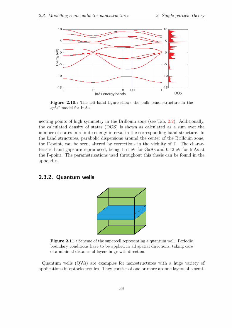
2.3. Modelling semiconductor nanostructures 2. Single-particle theory
-15
-10
-5
0
5
10
-15
-10
-5
0
5
10
L Γ X U,K Γ
Ener
gy (e
V)
InAs energy bands DOS
Figure 2.10.: The left-hand figure shows the bulk band structure in thesp3s∗ model for InAs.
necting points of high symmetry in the Brillouin zone (see Tab. 2.2). Additionally,the calculated density of states (DOS) is shown as calculated as a sum over thenumber of states in a finite energy interval in the corresponding band structure. Inthe band structures, parabolic dispersions around the center of the Brillouin zone,the Γ-point, can be seen, altered by corrections in the vicinity of Γ. The charac-teristic band gaps are reproduced, being 1.51 eV for GaAs and 0.42 eV for InAs atthe Γ-point. The parametrizations used throughout this thesis can be found in theappendix.
2.3.2. Quantum wells
Figure 2.11.: Scheme of the supercell representing a quantum well. Periodicboundary conditions have to be applied in all spatial directions, taking careof a minimal distance of layers in growth direction.
Quantum wells (QWs) are examples for nanostructures with a huge variety ofapplications in optoelectronics. They consist of one or more atomic layers of a semi-
38

2. Single-particle theory 2.3. Modelling semiconductor nanostructures
conductor material inside another semiconductor host material, for example InAslayers embedded in GaAs. Quantum wells are used as active laser material, switches,photodetectors and several other applications in modern telecommunication andelectronic devices. Because of the layer structure, the translational symmetry is lif-ted in growth direction (typically the [001]-direction in zincblende semiconductors)but still remains in the other two directions. In terms of our tight-binding modelthis means compared to the bulk case the Bloch-sums run only over these two dir-ections [110]. The structure in growth direction is represented in the Hamiltonianin which every layer is represented by a sub-block similar to the bulk matrix. Thematrix elements are given by:
HQWmν′α′,nνα =
∑R⊥
eik⊥R⊥ 〈R‖mν ′α′| H |R‖
n + R⊥να〉 . (2.93)
Here R‖m and R‖
n represent the z-positions of the atomic layers, R⊥ are the x- andy-components for nearest neighbours and k⊥ = (kx, ky, 0). The Hamiltonian thenincludes the layer-wise resolution and covers the anion-cation structure:
⎛⎜⎜⎜⎜⎜⎜⎜⎜⎜⎜⎜⎜⎜⎝
A C A C An = 0 n = 1 n = 2 n = 3 n = 4
A m = 0 AA AC ↑C m = 1 CA ↓ CC CA ↑A m = 2 AC ↓ AA AC ↑C m = 3 CA ↓ CC CA ↑
. . .
⎞⎟⎟⎟⎟⎟⎟⎟⎟⎟⎟⎟⎟⎟⎠
. (2.94)
Here the blocks αα with m = n and α ∈ {A, C} describe the on-site energies(and the couplings inside a layer if second next nearest neighbours are considered),αα′ ↑ with n − m = 1 describes the inter-layer coupling with the next higher
layer and αα′ ↓ describes the coupling with the next lower layer. It should beclear in this context, that ↓ and ↑ do indicate couplings and are not related to spindegrees of freedom. The single sub-blocks still include the structure factors and thetight-binding parameters, in a NN sp3s∗ model they have dimensions of 5x5 with13 independent empirical parameters. The relations between matrix elements andparameters are given by:
EsA = 〈R‖msA| H |R‖
m + R⊥sA〉 (2.95)VsApC = 4 〈R‖
msA| H |R‖m + R⊥pC〉 (2.96)
and likewise for all other elements [39]. As shown earlier, the directional cosines asgiven in Eqn. (2.27) and following equations weight the coupling parameters. Thisweighting stems from the decomposition of the orbitals into components of σ andπ-bonds in the two-center approximation. To trace back the matrix elements to
39

2.3. Modelling semiconductor nanostructures 2. Single-particle theory
common parameters, their order has to be changed for certain elements. With thatan additional sign enters the matrix elements according to the parity of the accordingatomic orbitals. s-, and s∗-like orbitals have even parity, p-like orbitals have oddparity. If the sum of the parity of the orbitals is even, changing the order of theorbitals does not change the sign of the matrix element. If the sum of the parity ofthe orbitals is odd, which is the case for couplings between s- and p-like orbitals forexample, changing the order of orbitals does change the sign of the matrix element:
〈ν| H |ν ′〉 =⎧⎨⎩+ 〈ν ′| H |ν〉 even parity sum of orbitals
− 〈ν ′| H |ν〉 odd parity sum of orbitals.(2.97)
In the sp3s∗-basis neglecting spin ( |α, s〉 , |α, px〉 , |α, py〉 , |α, pz〉 , |α, s∗〉 ) the sub-matrices read:
AC ↑ = ACparam ·
⎛⎜⎜⎜⎜⎜⎜⎝
s1 s2 s2 s1 0−s2 s1 s1 s2 −s2−s2 s1 s1 s2 −s2−s1 s2 s2 s1 −s1
0 s2 s2 s1 0
⎞⎟⎟⎟⎟⎟⎟⎠ (2.98)
CA ↓ = AC ′param ·
⎛⎜⎜⎜⎜⎜⎜⎝
s1 s2 s2 −s1 0−s2 s1 s1 −s2 −s2−s2 s1 s1 −s2 −s2
s1 −s2 −s2 s1 s10 s2 s2 −s1 0
⎞⎟⎟⎟⎟⎟⎟⎠ (2.99)
AC ↓ = ACparam ·
⎛⎜⎜⎜⎜⎜⎜⎝
s3 s4 −s4 −s3 0−s4 s3 −s3 −s4 −s4
s4 −s3 s3 s4 s4s3 −s4 s4 s3 s30 s4 −s4 −s3 0
⎞⎟⎟⎟⎟⎟⎟⎠ (2.100)
CA ↑ = AC ′param ·
⎛⎜⎜⎜⎜⎜⎜⎝
s3 s4 −s4 s3 0−s4 s3 −s3 s4 −s4
s4 −s3 s3 −s4 s4−s3 s4 −s4 s3 −s3
0 s4 −s4 s3 0
⎞⎟⎟⎟⎟⎟⎟⎠ (2.101)
with the abbreviations
s1 = eik⊥R⊥1 + eik⊥R⊥
2 (2.102)s2 = eik⊥R⊥
1 − eik⊥R⊥2 (2.103)
s3 = eik⊥R⊥3 + eik⊥R⊥
4 (2.104)s4 = eik⊥R⊥
3 − eik⊥R⊥4 (2.105)
40

2. Single-particle theory 2.3. Modelling semiconductor nanostructures
and
ACparam = 14
⎛⎜⎜⎜⎜⎜⎜⎝
Vss VsApC VsApC VsApC 0VpAsC Vxx Vxy Vxy VpAs∗C
VpAsC Vxy Vxx Vxy VpAs∗C
VpAsC Vxy Vxy Vxx VpAs∗C
0 Vs∗ApC Vs∗ApC Vs∗ApC 0
⎞⎟⎟⎟⎟⎟⎟⎠ (2.106)
to be multiplied elementwise. Here, R1 to R4 are the NN locations and the zerosexpress the assumption, that no couplings between s∗- and s-like-orbitals appear inthe model of [39].
Under inclusion of periodic boundary conditions this Hamiltonian still describesthe bulk material. To use periodic boundary conditions means periodicity at thesurfaces up to a phase factor given by eikzNa/4 = 1, N ∈ N being the number oflayers. Therefore the band structure consists of many sub-bands each with kz =Naπ/4 as shown in Fig. 2.12.
Figure 2.12.: Sub-bands for GaAs bulk material from the diagonalization ofthe QW Hamiltonian for N = 11 layers. Colored in red are the bulk bandsas calculated in the previous chapter. Deviations from the bulk bands stemfrom the different paths through the Brillouin-zone as indicated by L⊥ andX⊥
The consideration of spin-orbit coupling into the Hamiltonian follows exactly thesame steps as in the bulk case and therefore it doubles the Hamiltonian matrix size.
41

2.3. Modelling semiconductor nanostructures 2. Single-particle theory
Since it is assumed that only p-orbitals at the same atom are coupled via spin-orbitinteraction, the off-diagonal parts of the Hamiltonian stay the same, just accountingfor the bigger basis size:
AC ↑ so=
⎛⎝ AC ↑ 0
0 AC ↑ .
⎞⎠ (2.107)
The diagonal blocks become
αα =(
αα 00 αα
)+ SO α (2.108)
with
SO α = λα ·
⎛⎜⎜⎜⎜⎜⎜⎜⎜⎜⎜⎜⎜⎜⎜⎜⎜⎜⎜⎝
0 0 0 0 0 0 0 0 0 00 0 −i 0 0 0 0 0 1 00 i 0 0 0 0 0 0 −i 00 0 0 0 0 0 −1 i 0 00 0 0 0 0 0 0 0 0 00 0 0 0 0 0 0 0 0 00 0 0 −1 0 0 0 i 0 00 0 0 −i 0 0 −i 0 0 00 1 i 0 0 0 0 0 0 00 0 0 0 0 0 0 0 0 0
⎞⎟⎟⎟⎟⎟⎟⎟⎟⎟⎟⎟⎟⎟⎟⎟⎟⎟⎟⎠
. (2.109)
The parameter λα is defined by Eqn. (2.43).
Until this point it is just another and more complicated description of the bulkband structure; there is no quantum well included. The quantum well (let’s assumean InAs well in GaAs host material) is simulated by using the tight-binding InAsbulk parameters at the diagonal and off-diagonal Hamiltonian sub-blocks corres-ponding to the layers that form the quantum well and their couplings, respectively.Depending on which atom types form the surfaces between the two materials, theparameters are averaged as given by Eqn. (2.61). See [111] for a discussion of dif-ferent shapes and symmetries. In the case of InAs/GaAs quantum wells the twomaterials have common anions (the arsenic atoms). This situation is implementedby averaging the on-site parameters at the arsenic layers at the boundaries betweenthe quantum well and the host material. Couplings between this arsenic layer andthe surrounding layers hold InAs-related coupling parameters at the InAs-relatedsites and GaAs-related coupling parameters at the GaAs-related sites. In this spe-cial system no averaging of off-diagonal parameters is necessary. The part of the
42

2. Single-particle theory 2.3. Modelling semiconductor nanostructures
Hamiltonian describing the quantum well reads as follows:
HQW =
⎛⎜⎜⎜⎜⎜⎜⎜⎜⎜⎜⎜⎜⎜⎜⎜⎜⎜⎜⎜⎜⎜⎝
AA AC ↑CA ↓ CC CA ↑
AC ↓ AA AC ↑CA ↓ CC CA ↑
AC ↓ AA AC ↑CA ↓ CC CA ↑
AC ↓ AA
⎞⎟⎟⎟⎟⎟⎟⎟⎟⎟⎟⎟⎟⎟⎟⎟⎟⎟⎟⎟⎟⎟⎠
.
(2.110)Each block αα represents one layer of atoms (cations for α = C and anions forα = A) and each block αβ represents the coupling between two atomic layers.According to the parameters to be used in this model these blocks have differentcolours: GaAs-parameters are yellow, InAs-parameters are green. The blue blocksrepresent the common anion layers, where the parameters get averaged as
AA = 12
(AA + AA
). (2.111)
Another important fact to be accounted for in the tight-binding model stems fromthe situation that the energy bands of the different materials have to be aligned.The energy zero of band structure is generally free to be chosen as the valenceband maximum. In the case of two or more materials coming together these twoenergy scales have to be energetically related to each other. To incorporate this, asingle factor called the valence band offset ΔEv is introduced into the model whichis added to the on-site parameters of the well-material. This factor describes theenergetic distance of the valence band maxima of the materials4. In the literature,many values of ΔEv can be found, showing some controversy because of the hugedifferences. For the InAs/GaAs material system these values are between ΔEv =0.05 eV and ΔEv = 0.5 eV ([113–117]). Throughout this thesis we will use the valueof ΔEv = 0.06 eV as suggested in [113]. A more detailed discussion of the valenceband offset and its influence on electronic binding energies is given in Section 2.8.
In Figs. 2.13 and 2.14, the energy bands of a symmetric InAs quantum well con-sisting of 3 monolayers InAs inside a GaAs host matrix are shown. The quantumwell creates new sub-bands inside the bulk energy gap.
4In principle it does not matter if the energetic distance of the valence band maxima or at theconduction band minima is considered because one value sets the other and vice versa, see[112].
43

2.3. Modelling semiconductor nanostructures 2. Single-particle theory
Figure 2.13.: Energy bands of an InAs quantum well of three monolayers(green) in GaAs bulk material (red bands and grey sub-bands).
Figure 2.14.: As above, but a narrowed energy scale around energy zero isshown to emphasize the InAs quantum well bound energy bands (green) inthe vicinity of the Γ-point.
44
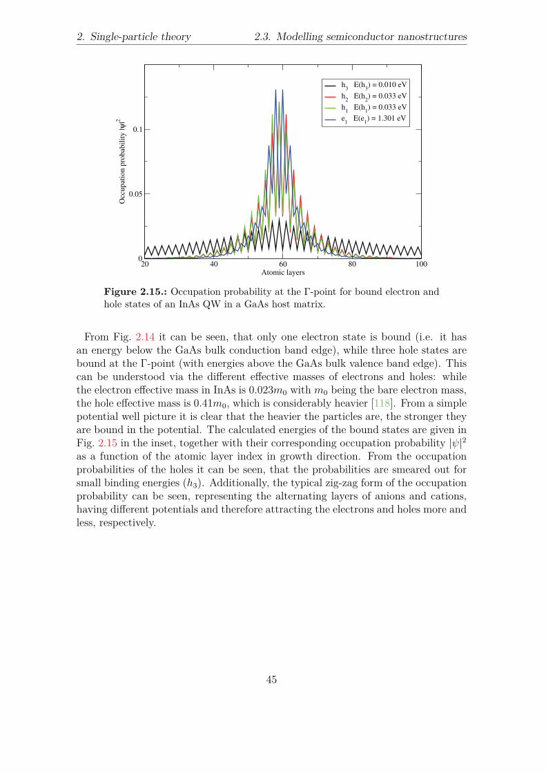
2. Single-particle theory 2.3. Modelling semiconductor nanostructures
20 40 60 80 100Atomic layers
0
0.05
0.1O
ccup
atio
n pr
obab
ility
|ψ|2
h3 E(h
3) = 0.010 eV
h2 E(h
2) = 0.033 eV
h1 E(h
1) = 0.033 eV
e1 E(e
1) = 1.301 eV
Figure 2.15.: Occupation probability at the Γ-point for bound electron andhole states of an InAs QW in a GaAs host matrix.
From Fig. 2.14 it can be seen, that only one electron state is bound (i.e. it hasan energy below the GaAs bulk conduction band edge), while three hole states arebound at the Γ-point (with energies above the GaAs bulk valence band edge). Thiscan be understood via the different effective masses of electrons and holes: whilethe electron effective mass in InAs is 0.023m0 with m0 being the bare electron mass,the hole effective mass is 0.41m0, which is considerably heavier [118]. From a simplepotential well picture it is clear that the heavier the particles are, the stronger theyare bound in the potential. The calculated energies of the bound states are given inFig. 2.15 in the inset, together with their corresponding occupation probability |ψ|2as a function of the atomic layer index in growth direction. From the occupationprobabilities of the holes it can be seen, that the probabilities are smeared out forsmall binding energies (h3). Additionally, the typical zig-zag form of the occupationprobability can be seen, representing the alternating layers of anions and cations,having different potentials and therefore attracting the electrons and holes more andless, respectively.
45

2.3. Modelling semiconductor nanostructures 2. Single-particle theory
2.3.3. Quantum dots
Figure 2.16.: Scheme of a three-dimensionally confined area of material inthe supercell, representing the QD.
Figure 2.17.: Exemplary supercell realization of a pure lens-shaped InAsQD. Red dots indicate Indium atoms, small blue dots indicate atoms belong-ing to the GaAs buffer.
In this chapter the calculation of bound single-particle energies and wave functionsof quantum dots on top of a wetting layer in a host matrix is explained in detail.Included is a overview of common quantum dot structures, benchmarks of our resultsas well as analysis of the influences of the different geometrical aspects of quantumdots on the electronic structure. Additionally the influences of Indium concentration,the choice of valence band offset and individual realizations is discussed.
When it comes to modelling quantum dots in the tight-binding approach, no morespatial periodicities can be used to simplify the corresponding Hamiltonian. Forthe description of three-dimensional nanostructures, each and every single atomin the spatial domain of interest has to appear as an individual subblock in theHamiltonian, a fact that blows up the computational needs drastically. The gen-eral structure of the Hamiltonian corresponds to the structure of the Hamiltonianused in the quantum well case, Eqn. (2.94). The difference is, that each subblockthat belonged to a single layer in the quantum well case now consists of numeroussubblocks itself, each representing an individual atom inside the layer. The atomicsubblocks hold the on-site energies and the spin-orbit terms of each individual atom.
46

2. Single-particle theory 2.3. Modelling semiconductor nanostructures
In second quantization, the unstrained TB Hamiltonian in its most general formreads as follows:
HT B =∑
Rνασ
Eαν |Rνασ〉 〈Rνασ|
+∑
R′ν′α′σ′,Rνασ
VR′α′ν′Rαν |R′ν ′α′σ′〉 〈Rνασ| (2.112)
with Eαν being the on-site energy of orbital ν at atom type α and VR′α′ν′Rαν beingthe hopping parameters between orbitals ν ′ and ν at atom type α′ at the atomicsite R′ and α at R, respectively.
The electronic wave functions are expressed as linear combinations of the atomicorbitals with complex expansion coefficients to be determined by diagonalization ofthe TB Hamiltonian:
ψ =∑
Rανσ
cRανσ |Rανσ〉 . (2.113)
In the sp3s∗ model including spin-orbit coupling five basis orbitals per atom perspin direction are assumed, which makes the size of the Hamiltonian 10N ×10N withN being the number of atoms in the computational domain for three-dimensionalcalculations. Without assuming the effect of spin-orbit coupling, the Hamiltonianis spin-independent and has the dimension 5N × 5N . For sake of simplicity we willdrop the spin-part for the moment. In that case the Hamiltonian looks like:
H =
⎛⎜⎜⎜⎜⎜⎜⎜⎝
Hon−siteα HNN
α,α′ 0 0 . . .HNN
α′,α Hon−siteα′ HNN
α′,α 0 . . .0 HNN
α,α′ Hon−siteα HNN
α,α′ . . .0 0 HNN
α′,α Hon−siteα′ . . .
... ... ... ... . . .
⎞⎟⎟⎟⎟⎟⎟⎟⎠
(2.114)
with the diagonal part holding the orbital energies
Hon−siteα =
⎛⎜⎜⎜⎜⎜⎜⎝
Eα,s 0 0 0 00 Eα,px 0 0 00 0 Eα,py 0 00 0 0 Eα,pz 00 0 0 0 Eα,s∗
⎞⎟⎟⎟⎟⎟⎟⎠ (2.115)
and the off-diagonal parts containing the NN hopping matrix elements
HNNα,α′ =
⎛⎜⎜⎜⎜⎜⎜⎝
V NNs,α,s,α′ V NN
s,α,px,α′ V NNs,α,py ,α′ V NN
s,α,pz ,α′ V NNs,α,s∗,α′
V NNpx,α,s,α′ V NN
px,α,px,α′ V NNpx,α,py ,α′ V NN
px,α,pz ,α′ V NNpx,α,s∗,α′
V NNpy ,α,s,α′ V NN
py ,α,px,α′ V NNpy ,α,py ,α′ V NN
py ,α,pz ,α′ V NNpy ,α,s∗,α′
V NNpz ,α,s,α′ V NN
pz ,α,px,α′ V NNpz ,α,py ,α′ V NN
pz ,α,pz ,α′ V NNpz ,α,s,α′
V NNs∗,α,s,α′ V NN
s∗,α,px,α′ V NNs∗,α,py ,α′ V NN
s∗,α,pz ,α′ V NNs∗,α,s∗,α′
⎞⎟⎟⎟⎟⎟⎟⎠ . (2.116)
47

2.3. Modelling semiconductor nanostructures 2. Single-particle theory
In general a NN sp3s∗ TB model yields 5 independent diagonal elements per atomtype and 25 hopping matrix elements per atom type as well as 25 matrix elementsper intertype coupling. So for GaAs (Gallium and Arsenic atoms) for examplethe model would need 5 + 5 + 25 + 25 + 25 = 85 different matrix elements to bedetermined empirically by fitting to an experimentally determined band structurealready in a nearest neighbour model. Luckily, in reality this is not the case. Dueto the assumed symmetry properties of the atomic orbitals (s-like, p-like symmetryetc.) and due to the model restrictions the number of free hopping parameters canbe reduced drastically. First, by limiting the distance up to which couplings aretaken into account, not every combination of couplings of atom types is allowed.Second, because of the orbital symmetries, several couplings are identical or zero:
Vs∗,α,s,α′ = Vs,α,s∗,α′ = Vs∗,α,s∗,α′ = 0. (2.117)
Because of the odd symmetry of p-like orbitals, simplifications as
Vpx,α,px,α′ = Vpy ,α,py ,α′ = Vpz ,α,pz ,α′ (2.118)Vs,α,px,α′ = −Vpx,α,s,α′ (2.119)Vs,α,py ,α′ = −Vpy ,α,s,α′ (2.120)Vs,α,pz ,α′ = −Vpz ,α,s,α′ (2.121)
Vs∗,α,px,α′ = −Vpx,α,s∗,α′ (2.122)Vs∗,α,py ,α′ = −Vpy ,α,s∗,α′ (2.123)Vs∗,α,pz ,α′ = −Vpz ,α,s∗,α′ (2.124)Vpx,α,py ,α′ = −Vpx,α,pz ,α′ (2.125)Vpx,α,py ,α′ = Vpy ,α,px,α′ (2.126)
can be used.
Then the nearest neighbour hopping submatrices can be written as:
HNNα,α′ =
⎛⎜⎜⎜⎜⎜⎜⎝
V NNs,α,s,α′ V NN
s,α,px,α′ V NNs,α,py ,α′ V NN
s,α,pz ,α′ 0−V NN
s,α,px,α′ V NNpx,α,px,α′ V NN
px,α,py ,α′ V NNpx,α,py ,α′ V NN
px,α,s∗,α′
−V NNs,α,py ,α′ V NN
px,α,py ,α′ V NNpx,α,px,α′ V NN
px,α,py ,α′ V NNpy ,α,s∗,α′
−V NNs,α,pz ,α′ V NN
px,α,py ,α′ V NNpx,α,py ,α′ V NN
px,α,px,α′ V NNpz ,α,s,α′
0 −V NNpx,α,s∗,α′ −V NN
py ,α,s∗,α′ −V NNpz ,α,s∗,α′ 0
⎞⎟⎟⎟⎟⎟⎟⎠ . (2.127)
These considerations reduce the number of independent parameters to 5 + 5 +7 + 7 + 7 = 31. We have assumed, that three of the basis orbitals hold p-likesymmetry: px,py and pz where the index x, y, z represents the different realizationsof the angular momentum quantum number. Since this has no influence on theorbital energy, the energies of these three orbitals equal each other. So per atomtype there are only three free parameters left for the orbital energies. Additionally,in a nearest-neighbour model for a common semiconductor material such as GaAs,
48
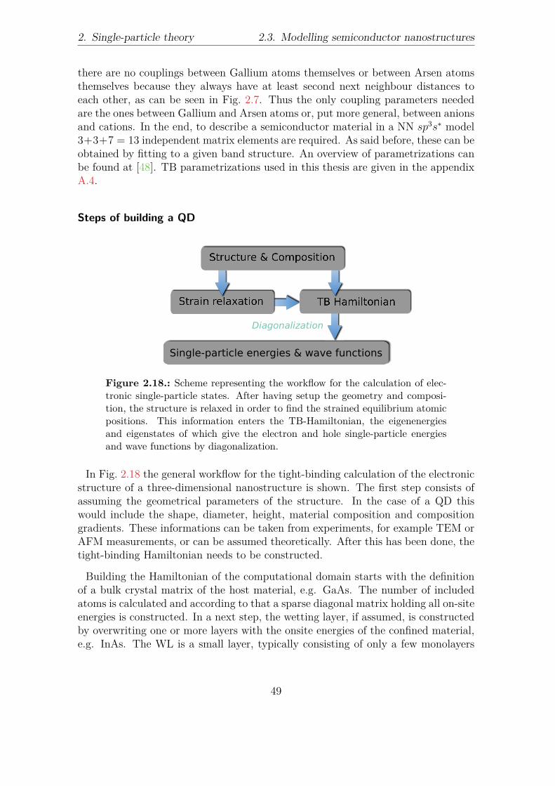
2. Single-particle theory 2.3. Modelling semiconductor nanostructures
there are no couplings between Gallium atoms themselves or between Arsen atomsthemselves because they always have at least second next neighbour distances toeach other, as can be seen in Fig. 2.7. Thus the only coupling parameters neededare the ones between Gallium and Arsen atoms or, put more general, between anionsand cations. In the end, to describe a semiconductor material in a NN sp3s∗ model3+3+7 = 13 independent matrix elements are required. As said before, these can beobtained by fitting to a given band structure. An overview of parametrizations canbe found at [48]. TB parametrizations used in this thesis are given in the appendixA.4.
Steps of building a QD
Figure 2.18.: Scheme representing the workflow for the calculation of elec-tronic single-particle states. After having setup the geometry and composi-tion, the structure is relaxed in order to find the strained equilibrium atomicpositions. This information enters the TB-Hamiltonian, the eigenenergiesand eigenstates of which give the electron and hole single-particle energiesand wave functions by diagonalization.
In Fig. 2.18 the general workflow for the tight-binding calculation of the electronicstructure of a three-dimensional nanostructure is shown. The first step consists ofassuming the geometrical parameters of the structure. In the case of a QD thiswould include the shape, diameter, height, material composition and compositiongradients. These informations can be taken from experiments, for example TEM orAFM measurements, or can be assumed theoretically. After this has been done, thetight-binding Hamiltonian needs to be constructed.
Building the Hamiltonian of the computational domain starts with the definitionof a bulk crystal matrix of the host material, e.g. GaAs. The number of includedatoms is calculated and according to that a sparse diagonal matrix holding all on-siteenergies is constructed. In a next step, the wetting layer, if assumed, is constructedby overwriting one or more layers with the onsite energies of the confined material,e.g. InAs. The WL is a small layer, typically consisting of only a few monolayers
49

2.3. Modelling semiconductor nanostructures 2. Single-particle theory
of the QD material, which is the central element in the Stranski-Krastanov growthmode, see appendix A.1.
On top of the wetting layer the quantum dot is built according to the chosengeometry. The most common geometries for InAs or InGaAs QDs on [001]-GaAsare lens- , disk- and pyramidal-shaped dots, sketched in Figs. 2.19, 2.20 and 2.21and discussed in the following. We will concentrate on lens-shaped dots here andshow results for the other shapes only for comparison. Those shapes are more orless roughly estimated: Often the dot-shapes are measured before overgrowth andmultiple steps of annealing, both effects of which are known as to change the shapedrastically due to several effects like interdiffusion, reordering and changes in thestrain-distribution. In a true atomistic model these effects have to be included atleast in considering InGaAs-QDs instead of pure InAs QDs: in reality no such thinglike a pure InAs QD would be realized because of the phenomena mentioned above.So in a realistic structure a QD always exhibits some fraction of the host materialinside the QD region. This effect is treated statistically: for a given target Indiumconcentration inside the dot region each cation atomic site is occupied with either anIndium or Gallium atom with a probability reflecting the target concentrations. Theeffect of this random alloy realization on single-particle energies and wave functionsis discussed in section 2.7.
After the QD is defined properly, new equilibrium positions for each atom due tothe arising lattice-mismatch induced strain are calculated employing molecular dy-namics simulation software5 via minimization of the global strain energy using theVFF as discussed in section 2.2.5. Afterwards, the strain-altered coupling matrixelements are introduced into the tight-binding Hamiltonian according to the ac-tual distribution of atoms and their equilibrium positions. As mentioned in section2.2.3 the couplings are treated in the two-center approximation. First, the bulkcoupling matrix elements are set according to which atoms are coupled, then thestrain-affected directional cosines are calulated (bond-bending term) and in the endthe product of both is multiplied with a factor that includes the new bond-length(bond-stretching term) to the power of the factor η. In a last step prior to thediagonalization the strain-independent spin-orbit splitting terms are included intothe Hamiltonian and the boundaries are set.
Common QD structures
In this Section, the three most common InAs quantum dot structures are discussedin terms of morphology and composition, as given in the literature. High-qualitysamples are often grown in MBE (molecular beam epitaxy), while low-cost samplesare grown in the MOVPE (metal organic vapor phase epitaxy) growth mode. Both
5See the appendix for a short introduction, LAMMPS material parameters for InAs and GaAsand best practice parameters.
50

2. Single-particle theory 2.3. Modelling semiconductor nanostructures
methods are sketched in the appendix A.1. During MBE, the growth can be mo-nitored in-situ by XPS methods (x-ray photoelectron spectroscopy), which give in-formation about the quantum dot formation and morphology for freestanding QDs.During overgrowth strain distributions change, lattice distortions arise and inter-diffusion of materials occurs due to different annealing steps [119–121]. Structuresof overgrown QDs can be investigated by TEM or related techniques, although fortransmission experiments a sample has to be cut in a thin slice to allow for transmis-sion of electrons. So TEM-pictures as given in [15] do not provide three-dimensionaldata about the QD morphology as it would be necessary as an input for a three-dimensional theory like tight-binding.
Likewise material concentrations inside and around the QD can only be measuredto a certain degree by TEM and averaging in direction of transmission over the wholeQD region cannot be avoided. Since complete knowledge about the QD features isnot achieveable it appears a good idea simulating different structures in theory toconclude to a most likely QD morphology by comparison of QD features like energylevels of bound states or exciton lines in the emission spectra [122–124]. Nevertheless,some information, at least in good approximation, is given about the QDs. Whatshould be kept in mind is that QD growth always is subject to fluctuations dueto temperature variations, local lattice imperfections or local strain changes anddue to the statistical nature of the growth itself. As a result of this, no QD iscompletely equal to another QD. There always are small deviations in size andcomposition which can be seen in comparing luminescence spectra of single quantumdots from the same sample or by high resolution spectroscopy of QD ensembles [125]which lead to slightly varying excitonic emission lines, both in energetic position andheight. One of the consequences of these small differences of energy levels and wavefunctions are slight changes in Coulomb interaction of carriers inside the QD, whichis the reason for the individual fine-structure splitting occuring in entanglementexperiments [124, 126]. This problem will be adressed in section 3.2.
Keeping the statistical nature of the growth process in mind, three main geometriesof InAs QDs can be identified, which are shown in the next sections.
Lens-shaped QDs
QDs indicating a lens-shape as shown in Fig. 2.19 can be assumed as the mostcommon QDs for InAs grown on a [001] GaAs substrate [35, 36, 75, 93, 127–138].To condense the information given in the literature, a typical lens-shaped InAs QD isbelieved to have a diameter of approximately 25 nm and a height of 2.3 nm to 3.3 nm.Indium concentrations range from In-rich (100-85% InAs in the QD region) to highlyannealed (60-10% InAs). Pure 100% InAs QDs are not believed to exist in nature butare useful model assumptions for a comparison between different theories becausestatistical fluctuations due to random alloying are avoided. Therefore, benchmarking
51

2.3. Modelling semiconductor nanostructures 2. Single-particle theory
Figure 2.19.: Atomistic supercell representation of a lens-shaped QD of pureInAs on top of a wetting layer, consisting of two monolayers InAs. Red andblue atoms are Indium and Arsenic atoms, respectively. Atoms belonging tothe GaAs buffer are not shown for illustration purposes and only a small partof the original supercell is shown.
will be done with pure InAs QDs.
Truncated pyramid-shaped QDs
QDs exhibiting the shape of a (truncated) pyramid as shown in Fig. 2.20 are assumedto have a side-length of about 20 nm and the height of 2.3 nm [86, 126, 139–141].These dots host a large percentage of Indium (approximately 100% InAs in the QDregion). Truncated pyramid-shaped QDs were often used for early k · p and TBcalculations.
Figure 2.20.: Atomistic supercell representation of a truncated pyramid-shaped QD of pure InAs on top of a wetting layer, consisting of two monolayersInAs. Atoms belonging to the GaAs buffer are not shown for illustrationpurposes. Only a small part of the original supercell is shown.
Disk-shaped QDs
Cylindrical QDs with a disklike shape are assumed to have a diameter of around20 nm and height of approximately 2.3 nm [128, 134, 142–148]. The InAs contentin these QDs is assumed to be around 60%. A model of the atomistic supercellrepresentation is shown in Fig. 2.21.
Also, combinations of the three geometries were observed, for example a disk-shaped dot with a reduction in diameter with increasing height [149].
52

2. Single-particle theory 2.4. Supercell requirements
Figure 2.21.: Atomistic supercell representation of a disk-shaped QD of pureInAs on top of a wetting layer, consisting of two monolayers InAs. Atomsbelonging to the GaAs buffer are not shown for illustration purposes. Only asmall part of the original supercell is shown.
2.4. Supercell requirements
As fabricated, QD sample and device sizes are in the order of centimeters, with real-istic quantum dot densities between 109 and 1012 per centimeter squared. Dependingon the aperture size, in photoluminescence measurements for example, a signal oftencomes from a large ensemble of QDs. Simultaneous atomistic simulation of the wholeensemble can only be treated by simple models such as the effective mass model,if the wavefunctions of individual QDs overlap and therefore influence each other.Three-dimensional models fail due to the problem size. For calculation of the opticalproperties of the ensemble Cluster-expansion methods can be used [150, 151].Mostrecent supercomputer calculations for the electronic structure feature quantum dotstacks with computational domains of around (110 nm)3 [152]. In more recent ex-periments, quantum dot densities can be lowered down experimentally to ultra lowdensities such as 107 QDs per centimeter squared [153], and techniques such as post-growth spatial selection and site-selective QD growth [154] allow for measurementson single QDs, integrated into devices like photonic or VCSEL-cavities.
In a tight-binding model this situation of a single QD with sizes ranging between5 and around 40 nanometers in diameter can be adressed. In recent years it becamepossible to even simulate QD molecules [77] and stacks of QDs [152] by means oftight-binding. Nevertheless, simulating a single QD can only cover a finite spatialregion, so it is necessary to treat the boundaries of the simulation domain appropri-ately.
As discussed in [155] there are different boundary conditions (BCs) possible tobe imposed on the Hamiltonian: open BCs, surface passivation and periodic BCs.Open BCs treat the surface of the tight-binding supercell as a transition from thecrystal to vacuum. This technique is known to produce unphysical surface stateswhich energetically lie inside the band gap [103]. Some effort is necessary to identifyand remove these states from the calculation, which is the reason why open BCsare used only in special geometries. One attempt to remove these states directly isto passivate the surfaces with hydrogen atoms. In the tight-binding formalism thismeans that all coupling matrix elements from surface atoms to atoms outside thesimulation domain are raised by several eV which shifts the energy of the surfacestates out of the band gap. Nevertheless, neither are the energies of the passivation
53

2.5. Diagonalization of large sparse matrices 2. Single-particle theory
atoms known, nor is it physically intuitive to passivate at all in a region of spacewhere the bulk material is located at. Another way of treating the surfaces is toimpose periodic BCs, so that the atoms at one surface of the domain are coupledto the atoms at the opposing surface of the domain. This approach corresponds tothe physical situation of placing QDs besides, on top and below each other with adistance of approximately the size of the simulation domain side-length. It appearsintuitive that in this case of BCs the simulation domain needs to be large enoughthat the QDs do not influence each other. This and the fact that the numericalbandwidth of the Hamiltonian matrix increases with using periodic BCs makes thischoice the computationally most demanding. Nevertheless, periodic BCs are usedin our model because it is the most realistic case and unphysical surface states donot appear.
2.5. Diagonalization of large sparse matrices
In general, the diagonalization of a matrix is a very basic piece of algebra as longas the matrix is small and fulfills some features such as invertibility. However, asproblems (matrix sizes) are getting larger and more complicated, the search foreigenstates and eigenvalues can be very difficult. Therefore the field of mathemat-ical research on efficient diagonalization algorithms is in neverending progress [156].Luckily, the Hamiltonian matrices arising in a tight-binding model fall in a classwhich fulfills some symmetries and characteristics that make the problem traceableand guarantee the existence of solutions. First of all, after Lowdin-orthogonalizationthe basis states are orthogonal and a standard eigenvalue problem has to be solved,yielding eigenpairs (eigenvalues and eigenstates):
Hψ = Eψ standardHψ = EBψ generalized,
where H is the Hamiltonian matrix, E are eigenvalues and ψ are the correspondingcomplex eigenstates. B would be another matrix which could arise for example instability analysis in fluid dynamics. The TB Hamiltonian matrix usually is hermitian(real eigenvalues), very sparse with a small bandwidth, complex (if spin-orbit split-ting is considered) and very large (of the order of 108 × 108). The sparsity usuallyis around 10−7.
In semiconductor nanostructures, only a few states are bound which lie in a definedregion of energy, most likely to be located inside the energy gap. So here we do notneed the information about all eigenpairs of the Hamiltonian matrix but only abouta very few eigenpairs with eigenvalues in the middle of the spectrum. Since thediagonalization of such a large matrix is not an easy task and convergence time is acrucial parameter, we use freely available software packages for efficient diagonaliz-ation. There are many different packages provided (for an overview see [157]), each
54

2. Single-particle theory 2.6. Benchmarks
suited for one or more special cases. We chose to use SLEPc [158], the ”ScalableLibrary for Eigenvalue Problem Computations”. This framework provides severalparallel spectral transformations and state-of-the-art eigensolvers based on PETSc[159], the ”Portable, Extensible Toolkit for Scientific Computation” which provides”a suite of data structures and routines that provide the building blocks for theimplementation of large-scale application codes on parallel (and serial) computers”[160, 161]. In our case it turned out that using the standard Krylov-Schur algorithm[162] in combination with the harmonic extraction technique [163, 164] is the bestchoice to find eigenpairs closest to a desired energy in terms of convergence speed.Best practice parameters for the use of PETSc and SLEPc are given in the appendix.
2.6. Benchmarks
In Fig. 2.22 GaAs band structures obtained from different TB models are compared.It can be seen, that the main differences occur in the conduction band far away fromthe Γ-point. The sp3s∗ model appears to be a good compromise between the sp3
and the sp3d5s∗ models. It captures the correct band gap and effective masses inthe vicinity of the Γ-point and resembles the splitting at X- and L-points quite well.Definitely, the sp3d5s∗ model captures more band structure features, but since weare interested in optical properties, the sp3s∗ model is well suited because opticaltransitions mainly occur between states around the smallest direct band gap, whichis at the Γ-point in conventional semiconductors. The band structure at the X-pointfor example becomes important for transport properties.
Figure 2.22.: GaAs band structure fits using different basis sizes in the em-pirical tight-binding model, from [165]. Red and green circles show discrep-ancy and agreement with experiment, respectively. The sp3d5s∗ model clearlyresembles the band structure best, but for applications happening mainly atthe Γ-point, the sp3s∗-basis is already sufficient.
55

2.6. Benchmarks 2. Single-particle theory
In Tab. 2.3 a comparison of QD single-particle energy gap (energetic distance ofground electron and hole states) and corresponding level splittings with results fromdifferent calculations from the literature using empirical pseudopotentials and thesp3d5s∗ TB model are shown. All calculations were carried out for a standard lens-shaped pure InAs QD with height of 3.5 nm and a diameter of 25 nm on top of awetting layer inside a GaAs host matrix, as displayed in Fig. 2.23.
Figure 2.23.: Atomistic representation of the pure InAs QD exhibiting lens-shape used to benchmark our TB model. From [75] for comparison.
Splitting EPP 1 EPP 2 Experiment TB 1 TB 2 Our results[35] [166] [167, 168] [75] [65]
e2 − e1 65 57 50 52.7 59.9 59.3e3 − e2 2 2.1 2 1.28 4.2 3.4e4 − e3 68 58 48 51.7 55.1 55.6h1 − h2 8 11 14.4 14.5 13.5h2 − h3 7 9 9.8 9.8 8.6h3 − h4 6 2.4 5.5 5.3 7.9EGap 796 732 749
Table 2.3.: Benchmark of our sp3s∗ TB model with results from differentother calculations (EPP 1, EPP 2, TB 1, TB 2) and with experimental data.Splittings between bound electron (e1..e4) and hole states (h1..h4) are com-pared as well as the single-particle energy gap EGap = e1 − h1. All values aregiven in meV.
EPP 1 and EPP 2 are calculations using the empirical pseudopotential modelwith different parametrizations, while TB 1 and TB 2 are tight-binding calculationswithin the sp3d5s∗ model including spin-orbit coupling and strain modifications viavalence force field strain minimization. From comparison of the energy splittings itcan be seen that the sp3s∗ TB model used in this thesis can compete with both, theadvanced sp3d5s∗ TB models as well as the pseudopotential models. Even betweenthe EPP and TB models themselves, differences of several meV between the energysplittings are observed, stemming from differences in the band structure paramet-rizations and strain parameters. This defines the accuracy of the energy levels tobe of the order of meV. Additionally, the EPP models use a modified valence forcefield including higher-order bond-stretching terms, while the TB models use an addi-tional modification of on-site parameters due to the strain-altered atomic positions.
56

2. Single-particle theory 2.7. Geometry and single-particle properties
Nevertheless, the basic energy level structure of the model QD is already covered inour more simple sp3s∗ TB model. Moreover, an astonishing agreement of our datawith the TB 2 results can be observed.
2.7. Geometry and single-particle properties
Having benchmarked the sp3s∗-TB model, in this section the single-particle electronand hole wave functions as calculated by our tight-binding model will be presentedand discussed for the common QD shapes, compositions and parameters. For com-parison, we assume a height of 2.2 nm and a diameter of 25 nm at QD base for alllens-shaped, truncated pyramid-shaped and disk-shaped geometry, respectively. AllQDs consist of pure InAs. After this comparison regarding the QD shape, we studythe influence of QD diameter and height as well as the Indium concentration fora lens-shaped QD. Additionally, the variation of the single-particle properties withdifferent individual atomic realizations is investigated.
Lens-shaped QDs
Figure 2.24.: Squared wave functions of the first 12 bound electrons (top)and holes (bottom) for a pure lens-shaped InAs QD. Each state is twofolddegenerate due to spin degree of freedom. Yellow lines indicate QD geometry.
In Fig. 2.24 the squared single-particle wave functions of electrons and holes for
57

2.7. Geometry and single-particle properties 2. Single-particle theory
the standard lens-shaped pure InAs QD are shown. In the upper half, the squaredelectron wave functions are depicted in side-view (first row) and in top-view (secondrow), while in the lower half the squared hole wave functions are given again in top-view (third row) and in side-view (fourth row). Occupation probabilities vary fromlow probability (dark blue) to high probability (dark red) on a color scale normalizedto the maximum occupation probability. Plots show summation over squared lattice-site eigenstate coefficients from the diagonalization of the TB Hamiltonian alonggrowth-direction for the top-view plots and along [010]-direction for side-view plots,respectively. Consequently, no absolute scale is given.
For the electrons, the lowest bound state is shown at the left side, having s-likesymmetry, followed by two perpendicular p-like states in the second and third columnfrom the left. The first three bound states having d-like symmetries are given inthe three columns on the right. All of these electron states show clear signaturesof the quantum harmonic oscillator states with increasing number of nodes of thewave functions with energy.
For the hole states, the deepest bound state is given in the left column, having s-like symmetry, followed, again, by two perpendicular aligned states with a somehowp-like symmetry. However, state mixing is larger for the holes, so the characteristicsof the quantum harmonic oscillator states are less pronounced. This can be seeneven better for the three states in the right columns.
From the side-view plots of both electron and hole squared wave functions it isvisible, that electron and hole states appear quite similar in this projection and thatthe center of the wave function tends to be closer to the base of the QD than to thetop, which can be interpreted as the influence of the wetting layer and QD shape.Note the difference in z-axis and x-axis: the z-axis has been magnified to show thewave functions properly.
Spin degeneracy is not shown, so each of the given states is doubly Kramers de-generate resulting in a total of twelve bound states given here. The total numberof bound states in this very geometry is very large indeed because of the maximumIndium concentration of 100 % assumed inside the QD.
In Tab. 2.4 the binding energies EB as defined by the energetic distance betweenthe energy corresponding to the state and the respective electron or hole wettinglayer band edge are given. Large binding energies are reached for both electronsand holes because of the large Indium concentration. Some general trends canbe identified from the energies. Because of the difference in effective mass butdepending on the valence band offset, electrons usually have larger binding energiesthan holes, while the intraband splittings are larger for electrons than for holes.Because of this, usually more hole states are bound despite their smaller bindingenergies. The intraband splittings of electrons usually exhibit a large-small-large-small structure which corresponds to the splittings between states with different
58
2. Single-particle theory 2.7. Geometry and single-particle properties
Electrons Holes Electrons HolesEB(n1) 385 259 n1 − n2 64.8 19.6EB(n2) 321 239 n2 − n3 3.0 8.5EB(n3) 318 230 n3 − n4 58.5 12.2EB(n4) 259 218 n4 − n5 2.5 11.3EB(n5) 257 207 n5 − n6 1.0 2.6EB(n6) 256 204EGap 759.65
Table 2.4.: In the left hand table the binding energies of the ground and firstfew excited bound electron and hole states for the standard lens-shaped pureInAs QD are shown. The index n corresponds to electrons (n = e) and holes(n = h). The right hand table shows the intraband splittings. Additionallythe single-particle energy gap EGap = e1 − h1 is given. All energies are inunits of meV.
symmetry being large and splittings between states with the same symmetry beingsmall. For example between the second and third electron state, both having p-like symmetry, the splitting is small (3 meV), as well as between the states havingd-like symmetry (2.5 and 1 meV). This energetic structure can be found in simpletwo-dimensional harmonic oscillator models, whereas the p- and d-like states aredegenerate there and the large splittings between these shells are equivalent. Forholes, this structure is spoiled. Splittings in general have a smaller amplitude andno clear large-small structure can be identified. Moreover, all splittings have similarvalues. In the last row of Tab. 2.4 the single-particle energy gap as defined byEGap = e1 − h1 = 759 meV is given, in good agreement with the literature, seeTab. 2.3.
Truncated pyramid-shaped QDs
In Fig. 2.25 the squared wave functions of the pure InAs QD with 2.2 nm height and25 nm diameter having the shape of a truncated pyramid are shown. The electronand hole wave functions appear quite similar to the ones from the lens-shaped QDbut account for the changes in geometry.
From the binding energies and intraband splittings for this geometry in Tab. 2.5 itcan be observed, that the confinement from the pyramid-shaped QD is larger thanfrom a lens-shaped QD, yielding larger binding energies for electrons (474 meV)and holes (290 meV). This results in a much smaller single-particle energy gap of639 meV, 120 meV smaller than for the lens-shaped QD. The bound state splittingsreveal an opposite trend for electrons and holes: electron splittings are smaller forthe pyramidal shaped QD than for the lens-shaped QD, while hole splittings show
59

2.7. Geometry and single-particle properties 2. Single-particle theory
Figure 2.25.: Squared wave functions of the first 12 bound electrons (top)and holes (bottom) for a pure InAs QD with the shape of a truncated pyramid.Each state is twofold degenerate due to spin degree of freedom. Yellow linesindicate QD geometry.
Electrons Holes Electrons HolesEB(n1) 474 290 n1 − n2 51.8 29.9EB(n2) 422 260 n2 − n3 1.4 6.4EB(n3) 420 254 n3 − n4 44.8 19.4EB(n4) 376 234 n4 − n5 19.7 2.7EB(n5) 356 232 n5 − n6 1.3 7.1EB(n6) 355 225EGap 639.82
Table 2.5.: In the left hand table the binding energies of the lowest boundelectron and highest bound hole states for the standard pure InAs QD withtruncated pyramid-shape are shown. The index n corresponds to electrons(n = e) and holes (n = h). The right hand table shows the intraband split-tings. Additionally the single-particle energy gap EGap = e1 −h1 is given. Allenergies are in units of meV.
the opposite behaviour. Also, the splitting between the two first electron d-likestates is largely increased. The hole states show a tendency of behaving more likein the harmonic oscillator case described above, resulting in the large-small-largesplitting energy structure.
60

2. Single-particle theory 2.7. Geometry and single-particle properties
Disk-shaped QDs
Figure 2.26.: Squared wave functions of the first 12 bound electrons (top)and holes (bottom) for a pure disk-shaped InAs QD. Each state is twofolddegenerate due to spin degree of freedom. Yellow lines indicate QD geometry.
In Fig. 2.26 the single-particle squared wave functions of electrons and holes areshown for the QD having disk-like shape. The symmetric geometry is clearly reflec-ted in the shape of the wave functions, for example the hole p-like states are nearlyrotationally symmetric.
Observing the binding energies and intraband splitting of the disk-shaped QD inTab. 2.6 reveals the trend from lens-shape to pyramid-shape ongoing to the disk-shape. Electron binding energies are enlarged further when compared to the pyramidshape, as well as hole binding energies. This leads to a further reduction in the single-particle energy gap to 604 meV. Electron splittings are also reduced further, whilehole splittings remain comparable to the hole splittings of the pyramid-shaped QD.The trend of hole splittings to a large-small-large energy structure is also furtherextended.
Variation of QD diameter
In Fig. 2.27 the variation of the first few bound electron and hole single-particleenergies with QD diameter are shown for a typical pure InAs QD having lens-shapewith a fixed height of 2.0 nm, which is lower than the previous QDs. The states
61

2.7. Geometry and single-particle properties 2. Single-particle theory
Electrons Holes Electrons HolesEB(n1) 491 309 n1 − n2 41.4 28.8EB(n2) 449 280 n2 − n3 1.3 3.5EB(n3) 448 276 n3 − n4 44.0 22.3EB(n4) 404 254 n4 − n5 1.9 2.9EB(n5) 402 251 n5 − n6 9.5 5.9EB(n6) 393 245EGap 604.20
Table 2.6.: In the left hand table the binding energies of the lowest boundelectron and highest bound hole states for the standard disk-shaped pureInAs QD are shown. The index n corresponds to electrons (n = e) and holes(n = h). The right hand table shows the intraband splittings. Additionallythe single-particle energy gap EGap = e1 − h1 is given. All energies are inunits of meV.
0 5 10 15 20 25 30QD diameter [nm]
1.1
1.2
1.3
1.4
1.5
1.6
Ene
rgy
[eV
]
GaAs band edge
sppd
Electron states
0 5 10 15 20 25 30QD diameter [nm]
0
0.05
0.1
0.15
0.2
0.25
0.3
0.35
0.4
0.45
sppd
Hole states
0 5 10 15 20 25 30QD diameter [nm]
0.8
1
1.2
1.4
Single-particle gap
GaAs band edge
Figure 2.27.: Variation of electron and hole single-particle total energieswith QD diameter (left hand and middle panel). In the right hand panel thevariation of the single-particle energy gap EGap = e1 − h1 is depicted.
having s, p, d-like orbital symmery are labelled s, p and d, respectively. As expectedfrom a simple quantum harmonic oscillator potential, the electron single-particle
62

2. Single-particle theory 2.7. Geometry and single-particle properties
energies are lowered with QD diameter and additional bound states appear, whilehole single-particle energies are raised. The overall energy gap as the differenceof electron and hole energies is lowered in a non-linear way while raising the QDdiameter. Note that the single-particle gap energies are raised in comparison tothe QDs before due to the smaller QD height, resulting in a weaker confinementpotential.
Variation of QD height
0 1 2 3 4 5 6 7QD height [nm]
1
1.2
1.4
1.6
Ene
rgy
[eV
]
sppd
Electron states
0 1 2 3 4 5 6 7QD height [nm]
0.1
0.15
0.2
0.25
0.3
0.35
sppd
Hole states
0 1 2 3 4 5 6 7QD height [nm]
0.8
0.9
1
1.1
1.2
Single-particle gap
GaAs band edge
Figure 2.28.: Variation of electron and hole single-particle energies with QDheight (left hand and middle panel). In the right hand panel the variation ofthe single-particle energy gap EGap = e1 − h1 is depicted.
In Fig. 2.28 the variation of electron and hole single-particle energies with QDheight is shown for typical heights ranging from one to seven nm with a fixed dia-meter of 15.8 nm. While the evolution of electron energies again can be explainedby the increase in confinement in growth direction, the behaviour of the hole en-ergies is more complex. First, the hole energies are raised for QD height changesfrom one to two nm, followed by an energetic decrease for larger QD heights. Thisbehaviour appears because of the complex interplay between strain distribution andcarrier confinement due to QD geometry. Nevertheless, the resulting single-particle
63
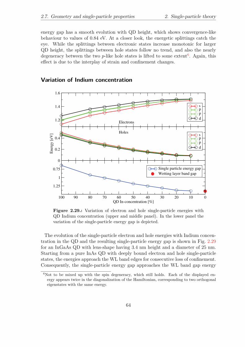
2.7. Geometry and single-particle properties 2. Single-particle theory
energy gap has a smooth evolution with QD height, which shows convergence-likebehaviour to values of 0.84 eV. At a closer look, the energetic splittings catch theeye. While the splittings between electronic states increase monotonic for largerQD height, the splittings between hole states follow no trend, and also the nearlydegeneracy between the two p-like hole states is lifted to some extent6. Again, thiseffect is due to the interplay of strain and confinement changes.
Variation of Indium concentration
1.2
1.4
1.6
Electrons
Holes
sppd
0
0.2
0.4
Ene
rgy
[eV
] sppd
0102030405060708090100QD In-concentration [%]
0.75
1
1.25
Single particle energy gapWetting layer band gap
Figure 2.29.: Variation of electron and hole single-particle energies withQD Indium concentration (upper and middle panel). In the lower panel thevariation of the single-particle energy gap is depicted.
The evolution of the single-particle electron and hole energies with Indium concen-tration in the QD and the resulting single-particle energy gap is shown in Fig. 2.29for an InGaAs QD with lens-shape having 3.4 nm height and a diameter of 25 nm.Starting from a pure InAs QD with deeply bound electron and hole single-particlestates, the energies approach the WL band edges for consecutive loss of confinement.Consequently, the single-particle energy gap approaches the WL band gap energy
6Not to be mixed up with the spin degeneracy, which still holds. Each of the displayed en-ergy appears twice in the diagonalization of the Hamiltonian, corresponding to two orthogonaleigenstates with the same energy.
64

2. Single-particle theory 2.7. Geometry and single-particle properties
for the complete absence of the QD. The WL Indium concentration is not changedin this calculations.
Averaging random realizations
As mentioned above, alloyed materials like InGaAs are modelled atomistically byrandom statistic distribution of the atoms. To illustrate the influence of these alloyfluctuations on the bound state energies, calculations for three random realizationsof a lens-shaped InGaAs QD with a nominal concentration of 30% Indium insidethe QD are summarized in Tab. 2.7.
Splitting Realization #1 Realization #2 Realization #3EB(e1) 74.9 74.6 74.2EB(h1) 32.4 34.5 32.6e1 − h1 1357.3 1355.5 1357.8e2 − e1 47.6 44.6 45.2e3 − e2 5.2 3 5.4e4 − e3 17.2 22.9 19.5h2 − h1 7.5 7.7 7.3h3 − h2 3.2 3.5 3.3h4 − h3 3.4 3.7 3.3
Table 2.7.: Influence of alloy fluctuations on lowest electron and hole bindingenergies (EB(e1) and EB(h1)), the single-particle energy gap e1 − h1 and theinterband splittings. All values are in meV.
It can be seen that the fluctuations in binding energies and the single-particlegap are of the order of 1-2 meV. Fluctuations of the intraband splittings show atendency of being larger, where the largest fluctuation is between e3 and e2 (5meV). These results can be compared with the literature for justification: in [169],a nearest neighbour sp3d5s∗ TB model was utilized for the repeated calculation ofsingle-particle energies of dome-shaped InGaAs QDs with 60% Indium content, adiameter of 30 nm and a height of 5.4 nm. The energetic variation at the band edgeswas calculated to have a distribution with width ±0.5 meV for holes and ±1 meVfor electrons, respectively, which is in very good agreement with our calculations.Nevertheless, the typical linewidth broadening measured in photoluminescence ex-periments on quantum dot ensembles [170, 171] is much higher because not only alloyfluctuations at the same Indium concentration occur but also size and compositionfluctuations due to the statistical nature of QD growth.
65

2.8. Choice of valence band offset 2. Single-particle theory
2.8. Choice of valence band offset
GaAs InAs
EInAs
GapEGaAs
Gap
ΔEV
Conduction-
band
Valence-
band
Figure 2.30.: Schematic energy diagram showing the band alignment atinterfaces between GaAs and InAs by means of the valence band offset ΔEv.The vertical axis labels energy, horizontal axis labels a spatial dimension, e.g.growth direction.
In a tight-binding calculation, the choice of the (unstrained) valence-band offsetΔEv seems to be a crucial parameter, because it determines the depth of the con-finement potential of both electrons and holes at once (see Fig. 2.30).
At a closer look, the choice of valence-band offset appears to be less important:as long as the number of confined states is high anyway, e.g. the Indium content ishigh, the influence of the choice of ΔEv on the band gap and the level splittings isnegligible. This was shown for example in [75], where a change of only 2% of theeffective gap was reported while going from ΔEv = 0.22 eV to ΔEv = 0.06 eV. Inthe present NN sp3s∗ TB model a change of 1.2% in the band gap was calculatedbetween ΔEv = 60 meV and ΔEv = 120 meV, in very good agreement with theliterature. On the other hand the choice of ΔEv becomes important in cases whereQDs have low Indium content, because in this case the number of confined statesis affected. This can lead to changes in the optical spectra due to a change in theconfiguration-interaction-basis7.
In the case of InAs QDs grown on GaAs the two materials form a type I interface(as sketched in Fig. 2.30). Since both materials share the same anions, the bandoffset tends to be rather small, according to the popular ”common-anion-rule” [172–174]. The values of ΔEv between GaAs and InAs interfaces in the literature span alarge range from only a few meV up to several hundreds of meV [113–115]. See [117]
7The CI basis consists of all bound quantum dot states, at least in a full-CI treatment, to beintroduced in section 3.1
66

2. Single-particle theory 2.8. Choice of valence band offset
60 80 100 120Valence band offset [meV]
1.4
1.45
1.5
1.55E
nerg
y [e
V]
sppd
Electron states
60 80 100 120Valence band offset [meV]
0.03
0.045
0.06
0.075
0.09
sppd
Hole states
60 80 100 120Valence band offset [meV]
1.365
1.3675
1.37
1.3725
1.375
Single particle gap
Figure 2.31.: Dependence of electron and hole single-particle energies (lefthand and middle panel) and energy gap (right hand panel) on the choice ofvalence band offset ΔEv.
and [175] for reviews. Since there is no accepted value for the valence band offsetbetween GaAs and InAs we use a rather small value of 60 meV from [113], providingthe best agreement with other calculations for the benchmark given in section 2.6.
In Fig. 2.31 the dependence of the single-particle electron and hole energies on thevalence band offset ΔEv is shown as well as the single-particle energy gap. ΔEv wasvaried between 60 meV and 120 meV and a disk-shaped QD with diameter of 18 nm,height of 2.0 nm and an Indium concentration of 30% was assumed, similar to [176].Bound electron and hole energies both show only a small dependence on the offset.While the raise of electron energies with the valence-band offset leads to smallerbinding energies, the raise of hole energies leads to larger binding energies. Thisbehaviour simply reflects the increase and decrease in depth of the confinementpotentials for electrons and holes, respectively, as mediated by the valence-bandoffset.
67

2.9. Number of bound states 2. Single-particle theory
2.9. Number of bound states
The number of bound electron and hole states is an important parameter for applica-tions. It is mainly influenced by the depth of confinement (the Indium concentrationin InGaAs QDs) and the geometry of the QD. Following the picture of a quantumharmonic oscillator, the number of confined hole states should always outnumberthe number of confined electron states if the potential is equally deep, which wouldbe the case for valence band offset and conduction band offset being equal. Thereason for this is the larger effective mass of holes in the crystal, bringing the holestates closer together. In general, the two band-offsets are not equal, so the num-bers of confined electron and hole states are independent. As the criterion for anelectron (hole) state being confined in the nanostructure, two different methods canbe applied.
As a first method the part of the occupation probability |ψ|2 of the state underconsideration inside the QD can be used as a measure for the state being boundor unbound. A certain number has to be defined as a threshold: If the part ofthe occupation probability inside the QD is larger (smaller) than the threshold, thestate is considered as bound (not bound).
The second method utilizes the energy of the state to define whether it is boundor not. To do this, an independent calculation has to be carried out considering anempty system without the QD, only consisting of the WL inside the supercell. Theband edges of this system, which are the highest WL hole state and the lowest WLelectron state, are used to define the binding energies of the QD system. An electron(hole) is considered bound, if the corresponding energy is lower (higher) than theWL electron (hole) band edge. This energetic difference defines the binding energyof the bound states. Intuitively, a state with a positive binding energy is bound,while negative binding energies define unbound states.
Here, we use the second criterion since it introduces no artificial threshold andtherefore appears natural to use.
Figure 2.32.: WL system consisting of two monolayers of InAs. Anions andcations of InAs are shown red and blue, while atoms belonging to the GaAsbuffer are not shown for illustration.
In the following, calculations of the number of bound states were carried out fortypical InGaAs QDs with low Indium concentration between 15% and 30%. The QDsare modelled lens-shaped with a height of 2.2 nm and a diameter of approximately25 nm. The WL is assumed to have a height of two monolayers as shown in Fig. 2.32.The calculated WL band edge energies are given in Tab. 2.8.
68

2. Single-particle theory 2.9. Number of bound states
eW L1 [eV] hW L
1 [eV]1.4676 0.0629
Table 2.8.: Calculated band-edge energies of the InAs WL system which areused as reference to decide between bound and unbound QD-states.
As stated above, these energies are subject to the band offsets, the valence forcefield parametrization and, of course, the tight-binding parametrization.
In Fig. 2.33 the occupation probability for the ground hole WL state are visu-alized as cuts through the supercell representation in side-view. As expected, theprobabilities reflect the translational symmetry of the WL perpendicular to growthdirection and are symmetric around the WL center in growth direction.
Figure 2.33.: Exemplary visualization of the occupation probability of thehole WL ground state in side-view (along the [010] crystal direction). Blueand red colors correspond to low and high occupation probability, respectively.
Having calculated the reference energies of the WL, the binding energies for dif-ferent Indium concentrations of the QD were extracted. Results are presented inTab. 2.9 for electrons and Tab. 2.10 for holes, respectively. Each listed energy rep-resents a twofold spin degenerate bound state. Empty cells represent the onset ofthe continuum of delocalized states.
Quite intuitively, we observe that the number of bound states increases for largerIndium concentration, i.e. for a deeper confinement potential. For a typical QD asobserved in experiments having an average Indium concentration of 20%, due to ourcalculations three electrons and five holes are expected to be bound. Experimentsshow typical number of bound states of one to four spin-degenerate energy levels[177]. For smaller QD Indium concentrations than 15% only one electron and holeare expected to be bound, having an energy approaching the WL band edges for
69

2.9. Number of bound states 2. Single-particle theory
conc. [%] EGap [eV] e1 e2 e3 e4 e5 e6
15 1.3667 26.3 3.3 2.417.5 1.3565 33.4 8.9 6.220 1.3444 41.7 14.6 13.5
22.5 1.3312 50.5 22.0 20.825 1.3175 59.1 29.7 28.0 3.9 1.930 1.2924 78.01 45.01 41.51 15.11 11.41 9.91
Table 2.9.: Electron binding energies and single-particle energy gap as afunction of InGaAs QD Indium concentration. All energies are given in unitsof meV unless stated otherwise.
conc. [%] h1 h2 h3 h4 h5 h6
15 10.644 4.144 2.89417.5 13.704 7.014 5.614 0.73420 17.534 10.104 8.514 3.024 1.144
22.5 21.974 14.564 13.054 7.074 4.474 3.76425 27.014 19.454 16.934 10.874 8.034 6.81430 34.19 24.52 22.56 15.68 13.31 12.16
Table 2.10.: Hole binding energies as a function of InGaAs QD Indiumconcentration. All energies are given in units of meV unless stated otherwise.
Indium concentrations approaching zero.
From the calculated energies we can extract the following trends. Electron bind-ing energies are growing faster than hole binding energies with increasing Indiumconcentration due to their lower effective mass. While splitting between the firstand the second bound state (s- and p-like symmetries) gets larger with increasingIndium concentration, the splittings between the two nearly degenerate states withboth p-like symmetry remain approximately constant for both electrons and holes.
70

3. Many-particle theory
Contents3.1. Full Configuration Interaction . . . . . . . . . . . . . . . . 73
3.1.1. Coulomb matrix elements from TB wave functions . . . . 763.1.2. Many-particle states . . . . . . . . . . . . . . . . . . . . . 783.1.3. Dipole matrix elements from TB wave functions . . . . . 793.1.4. Excitonic spectrum . . . . . . . . . . . . . . . . . . . . . . 84
3.2. Excitonic fine-structure splitting . . . . . . . . . . . . . . 86
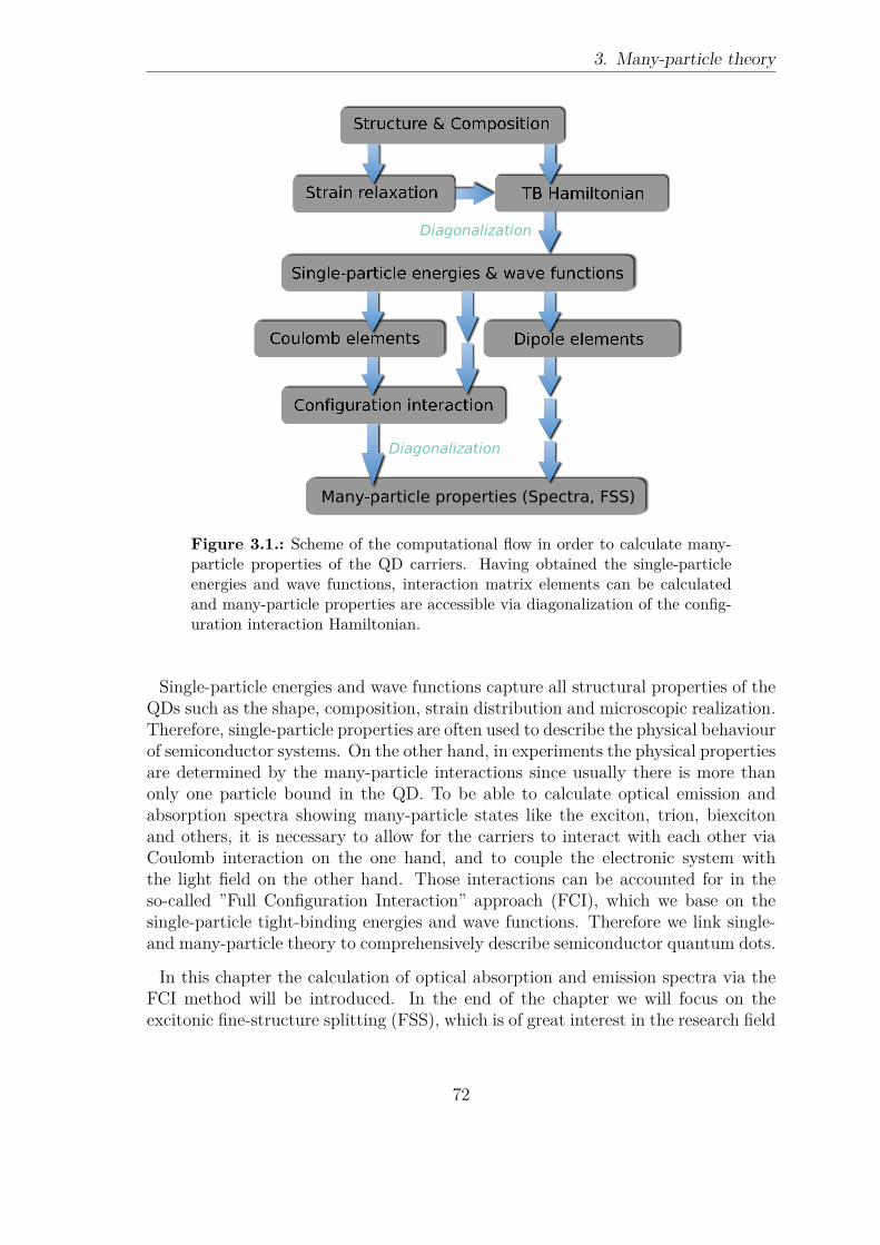
3. Many-particle theory
Figure 3.1.: Scheme of the computational flow in order to calculate many-particle properties of the QD carriers. Having obtained the single-particleenergies and wave functions, interaction matrix elements can be calculatedand many-particle properties are accessible via diagonalization of the config-uration interaction Hamiltonian.
Single-particle energies and wave functions capture all structural properties of theQDs such as the shape, composition, strain distribution and microscopic realization.Therefore, single-particle properties are often used to describe the physical behaviourof semiconductor systems. On the other hand, in experiments the physical propertiesare determined by the many-particle interactions since usually there is more thanonly one particle bound in the QD. To be able to calculate optical emission andabsorption spectra showing many-particle states like the exciton, trion, biexcitonand others, it is necessary to allow for the carriers to interact with each other viaCoulomb interaction on the one hand, and to couple the electronic system withthe light field on the other hand. Those interactions can be accounted for in theso-called ”Full Configuration Interaction” approach (FCI), which we base on thesingle-particle tight-binding energies and wave functions. Therefore we link single-and many-particle theory to comprehensively describe semiconductor quantum dots.
In this chapter the calculation of optical absorption and emission spectra via theFCI method will be introduced. In the end of the chapter we will focus on theexcitonic fine-structure splitting (FSS), which is of great interest in the research field
72

3. Many-particle theory 3.1. Full Configuration Interaction
concerning new devices for quantum information processing and quantum crypto-graphy [178]. As shown in Fig. 3.1, the single-particle energies and wave functionscalculated using the TB model are taken as input for the FCI and for the derivationof matrix elements in order to calculate optical spectra. In the following we doneglect electron-phonon interactions. Treating this interaction correctly would betopic for another thesis, see [179] for example.
3.1. Full Configuration Interaction
The most important mechanism for electrons and holes to interact is the Coulombinteraction. Two particles influence each other by renormalization of their energiesand wave functions and to be precise, there is no such thing as two individualparticles inside a quantum dot because their individual properties arise from theexistence of the other particle. For example a pair of one bound electron and onebound hole form a quasiparticle called exciton because of the attraction caused bythe opposite charges. Two electrons repulse each other, which also renormalizesthe energies. If there is a third charge inside the dot, the quasiparticle trion plus ortrion minus is built, depending on whether the third particle has positive or negativecharge. Additionally, bound carriers in the QD are embedded in a matrix of bulkmaterial with a continuum of delocalized carrier states, which gives rise to energyrenormalizations due to the coupling to phonons (forming a new quasiparticle calledpolaron).
Since for our needs this renormalizations are of minor interest, we neglect them.For further information on carrier-phonon interaction see [179].
In the ”Full Configuration Interaction” approach [180, 181] the Coulomb inter-action between all bound single-particle states is taken into account. The FCI-Hamiltonian is formulated in the basis of single-particle configurations in whichmatrix elements for the Coulomb interaction are added. An example of these con-figurations is shown in Fig. 3.2, adopted from [19]. Since the Hilbert space for thisproblem grows exponentially with the number of states in consideration, and sincein QDs showing strong carrier confinement (large QDs in size and/or QDs with ahigh Indium content) many bound states can be occupied by carriers, the numberof states in the FCI is often reduced artificially. In this case, the Hilbert space istruncated and only the first few bound states for electrons and holes are taken intoaccount. For such a truncation the method is called ”Configuration Interaction”(CI) only.
The FCI Hamiltonian readsHFCI = H0 + HC , (3.1)
allowing the free particles (H0) to interact via Coulomb interaction (HC). Intro-
73

3.1. Full Configuration Interaction 3. Many-particle theory
Figure 3.2.: Examplary single-particle configurations for a QD having twoconfined states both for electrons and holes in the electron-hole picture, from[19]. For simplicity only one spin direction and only configurations with aneven number of carriers are assumed. The s-states are labelled |2〉 and |3〉while p-states are labelled |1〉 and |4〉. From left to right these configura-tions are: the empty dot; the exciton with the carriers occupying the s-shells(ground state exciton 1XS); the p-exciton 1XP ; the biexciton 2XSP ; the p-s-exciton 0XP ; the s-p-exciton 0XS . Charged configurations with an oddnumber of carriers are not shown here.
ducing quasi-particle creation and annihilation operators λ†i and λi where λ†
i (λi) iseither an operator on the electron- (λ = e) or hole-subspace (λ = h) creating (an-nihilating) an electron (hole) in the single-particle state i, the free particle part ofthe Hamiltonian is given by
H0 =∑
i
(εe
i e†iei + εh
i h†ihi
). (3.2)
Here, εei and εh
i are the single-particle electron and hole energies of state i ascalculated by TB theory. The Hamiltonian HC , allowing for carrier-carrier interac-tion between configurations, reads
HC =∑ijkl
Vλiλjλkλl
ijkl λ†iλ
†jλkλl . (3.3)
In the above equation, Vλiλjλkλl
ijkl are the Coulomb matrix elements (CME) betweenparticles in the states i, j, k and l. Depending on the operator sequence three cat-egories of these matrix elements can be identified:
1. Band-diagonal interaction elements: λ†iλ
†jλkλl = e†
ie†jekel or h†
ih†jhkhl
2. Electron-hole direct interaction elements: λ†iλ
†jλkλl = e†
ih†jhkel or h†
ie†jekhl
3. Electron-hole exchange interaction elements: λ†iλ
†jλkλl = e†
ih†jekhl or h†
ie†jhkel .
The first category describes the simple repulsion between two carriers with equalcharge. Following the operator notation, this process can be expressed as the an-nihilation of two carriers in the states k and l and the creation of two carriers in
74

3. Many-particle theory 3.1. Full Configuration Interaction
the states i and j. The second category describes the direct attraction of carrierswith different charge, where for example an electron in the state k and a hole in thestate l are annihilated and an electron in state i and a hole in state j are created.The third category corresponds to the process of electrons and holes exchangingtheir states during the interaction. This interaction process occurs because of theundistinguishability due to the quantum nature of these particles. Although elec-trons and holes can be distinguished by their respective mass, these processes occurand therefore the matrix elements exist. Usually these interactions are neglected[127] because they have considerably smaller amplitude in comparison to the directterms. Throughout this thesis these matrix elements are calculated explicitely sincethey are partly responsible for the excitonic fine-structure splittings. Showing allthese processes as single contributions the FCI-Hamiltonian reads:
HF CI = H0 + HC
=∑
i
(εe
i e†iei + εh
i h†ihi
)
+ 12
∑ijkl
V eeeeijkl e†
ie†jekel + 1
2∑ijkl
V hhhhijkl h†
ih†jhkhl
− ∑ijkl
V ehheijkl e†
ih†jhkel − ∑
ijkl
V heehijkl h†
ie†jekhl
− ∑ijkl
V ehehijkl e†
ih†jekhl − ∑
ijkl
V heheijkl h†
ie†jhkel . (3.4)
The factor of 12 appears to avoid double counting. The minus sign in the electron-hole
interactions appears due to the attractive nature of the different charges, the plussign in the electron-electron and hole-hole interactions accounts for the repulsionbetween carriers of the same charge. To calculate the arising many-particle energiesand wave functions, this Hamiltonian has to be diagonalized. The eigenenergiescorrespond to the many-particle energies as seen in experiments, the eigenstates ofthe Hamiltonian give the many-particle states in terms of mixing coefficients for thesingle-particle configurations.
75

3.1. Full Configuration Interaction 3. Many-particle theory
3.1.1. Coulomb matrix elements from TB wave functions
In general, direct and exchange Coulomb matrix elements between carriers can becalculated by spatial integration of the corresponding carrier wave functions withthe Coulomb potential:
V dirijkl = e2
4πεε0
∫∫ ψ∗i (r1)ψ∗
j (r2)ψk(r2)ψl(r1)|r1 − r2| dr1dr2 (3.5)
V exchijkl = e2
4πεε0
∫∫ ψ∗i (r1)ψ∗
j (r2)ψk(r1)ψl(r2)|r1 − r2| dr1dr2. (3.6)
Here ψ(r) are the single-particle wave functions. The prefactor consists of thecharges and the material dependent relative permittivity ε and the vacuum per-mittivity ε0 (dielectric constant).
As shown in chapter 2.3.3, diagonalization of the tight-binding Hamiltonian inthe basis of atomic orbitals yields the wave function coefficients in this basis. Onlyknowledge about the orbital symmetries, spatial orientations and energies entersthe calculation, whereas no information about the basis functions is needed. Nowfor the calculation of the Coulomb matrix elements above, those basis functions areneeded explicitly, at least in principle. However, due to the long-range nature ofthe Coulomb interaction, the basis functions intuitively appear less important thanthe overall variation of the wave function which enter the integral. Therefore, it ispossible to approximately calculate the Coulomb matrix elements from the tight-binding coefficients directly. For a deeper discussion follow the appendix of [112].We can use the tight-binding wave functions
ψ(r) =∑R
cR(R)φR(r) (3.7)
with the generalized index R = {Rανσ} for the calculation of the Coulomb matrixelements. φR(r) = 〈r|R〉 are the (unknown) spatial representations of the basisorbitals. We plug Eqn. (3.7) in Eqn. (3.5), yielding:
V dirijkl =
∑R1R2R3R4
ci∗R1
cj∗R2
ckR3
clR4
∫∫dr1dr2V (r1 − r2) φ∗
R1(r1)φ∗
R2(r2)φR3(r2)φR4(r1)
(3.8)with the Coulomb potential
V (r1 − r2) = e2
4πεε0|r1 − r2| . (3.9)
The variation of the wave functions within the interatomic distance, φ(r), is unknownand aassumed to be of minor importance. Nevertheless, as before, it turns out
76

3. Many-particle theory 3.1. Full Configuration Interaction
QD shape V hhhh1111 V eeee
1111 V ehhe1111 V eheh
1111
lens 30.37 33.57 31.66 0.25pyramid 32.77 27.81 29.91 0.33
disk 30.34 24.69 27.02 0.26
Table 3.1.: Typical values of the Coulomb matrix elements for combinationsof the s-like electron and hole states for the three standard quantum dots ex-aminated in the single-particle theory section as calculated from tight-bindingwave function coefficients. All values are given in units of meV.
that Eqn. (3.8) can be approximated by using only the tight-binding wave functioncoefficients, which are defined on the discrete grid of (relaxed) atomic sites:
V dirijkl ≈ ∑
R1R2
ci∗R1
cj∗R2
ckR2
clR1
V (R1 − R2) (3.10)
where the potential now is a function of differences in atomic sites:
V (R1 − R2) =
⎧⎪⎨⎪⎩
e2
4πεε0|R1−R2| for R1 �= R21
Vuc
∫uc
dr1dr2e2
4πεε0|r1−r2| ≈ Vc for R1 = R2.(3.11)
Here, Vc is a constant energy to be calculated only once and Vuc is the unit cellvolume.
The approximation of using tight-binding wave function coefficients only is validbecause of the long-ranging behaviour of the Coulomb interaction [112]. For numeri-cal reasons the summations over lattice points for the calculation of the CMEs arecarried out in the Fourier transformed basis [182]. Since the choice of the relativepermittivity ε of the material surrounding the interacting carriers is not straight-forward, we use the mean value for the materials occupying the supercell for thescreening. In the case of InAs and GaAs this is a rather good choice, because theconstants are quite similar: εInAs = 12.3 and εGaAs = 10.89 (both at room temper-ature [118]). In Tab. 3.1 we show typical values for the calculated Coulomb matrixelements between s-like single-particle states for the three standard QDs as definedin section 2.7 indicating the energy scales of direct and indirect Coulomb matrixelements in the InGaAs material system.
We can see that the direct Coulomb matrix elements all have the same energy scale,varying only within a few meV, while the exchange matrix elements are smaller by afactor of around 100. These values are in good agreement with typical magnitudesof the Coulomb matrix elements in the InAs/GaAs material system.
Once calculated, with these matrix elements the many-particle states can be de-rived from the diagonalization of the FCI-Hamiltonian. For the consecutive calcula-tion of optical spectra featuring realistic relative peak heights, information is needed
77
3.1. Full Configuration Interaction 3. Many-particle theory
about the strengths of optical transitions between the carrier configurations, whichare represented by the dipole matrix elements.
3.1.2. Many-particle states
Having calculated the Coulomb matrix elements for carrier-carrier interaction be-tween bound states in the quantum dot as discussed in the previous section, Coulomb-mediated many-particle states of the quantum dot can be calculated by numericaldiagonalization of Eqn. (3.4). This diagonalization is carried out in the basis ofsingle-particle configurations, giving the coefficients for linear combinations of thebasis states.
For simplicity and numerical reasons we truncate the many-particle Hilbert spacein two ways. Since the number of configurations scales as 2N , with N being thenumber of single-particle states under consideration, the size of the Hilbert space isvery large even for quantum dots with a medium confinement (medium-sized dotsand/or intermediate Indium content). Only very few quantum dot experiments showconfinements large enough to have more energy levels confined than the lowest levelswhich can be identified as s-, p- and d-like states. This is mostly due to the averageIndium content being smaller than 20% in most experiments. Additionally, consi-dering optical or electrical pumping of the quantum dot levels, the recombinationtimes usually are fast enough to keep only the few lowest energy levels occupiedwith carriers.
With these considerations in mind we truncate the Hilbert space to particle num-bers not exceeding 6, i.e. taking only s- and p-like states into account. With thiswe neglect small renormalizations of the many-particle energies because of the ener-getically higher lying states, but taking into account this d-like states would alreadyenlarge the Hilbert space enormously. The other truncation of the Hilbert spacewe carry out is not necessary but keeps the spectra simple to interpret. We reducethe basis to configurations that conserve the number of particles in a way, that onlyconfigurations having the same number of electrons and holes form the basis. Withthis truncation we neglect charged excitons (X1±, X2±, ..) but speed up the diagon-alization procedure. Optical quantum dot spectra as investigated in this thesis aredetermined mainly by the direct excitonic transitions, as can be seen by the dipolematrix elements (to be discussed in the next section), so this second truncationappears to be a good approximation.
78

3. Many-particle theory 3.1. Full Configuration Interaction
3.1.3. Dipole matrix elements from TB wave functions
For the calculation of optical emission and absorption spectra from semiconductorquantum dots it is necessary to describe the interaction of the quantum dot carrierswith the electromagnetic field. In the literature there are elaborated methods toincorporate magnetic and electric fields directly into the tight-binding Hamiltonian[183, 184]. These methods are used for strong fields which influence the orbitalenergies and therefore have a direct impact on the single-particle energies. For weakfields, which vary slowly on the scale of typical quantum dot sizes, it is sufficient totreat the interaction in the widely used dipole approximation.
Within this approximation the light-matter coupling of a dipole d in an electricfield E is given by the dipole Hamiltonian
HD = −dE. (3.12)
Without any loss of generality, we assume a linearly polarized electric field E(r,t)with the direction of propagation along the wave vector k
E(r, t) = E[klm]0 ei(kr−ωt) (3.13)
with E[klm]0 = (Ek
0 , El0, Em
0 ) being the polarization vector with lattice parameters k, land m and ω being the frequency. In our cases the polarization will most likely bealong the [110] and [110] crystal directions, perpendicular to the growth direction.This results in
E[110]0 = 1√
2(1, 1, 0) (3.14)
andE[110]
0 = 1√2
(1, −1, 0), (3.15)
respectively. Considering emission from a quantum dot excitonic recombination, theabsolute values of k and r can be estimated as
|k| · |r| ≈ 2π
λ· 10nm ≈ 2π
1000nm · 10nm ≈ 0.06 � 1. (3.16)
Here we used a spatial distribution of the exciton wave function of 10 nm [185], whichis strongly localized in a quantum dot emitting at a typical emission wavelength ofaround 1000 nm for InGaAs quantum dots. |k| · |r| � 1 translates into the fieldvarying only slowly on the QD scale, the dipole approximation can be used, whichmeans neglecting the spatial variation of the electric field.
Writing the approximate dipole Hamiltonian gives
HD = −dE[klm]0 (3.17)
79

3.1. Full Configuration Interaction 3. Many-particle theory
or, in second quantization,
HD = −Ne∑i=1
Nh∑j=1
[Dij c†e,ic
†h,j︸ ︷︷ ︸
absorption
+D∗ij ce,ich,j︸ ︷︷ ︸
emission
] (3.18)
with Ne and Nh being the number of single-particle bound states of electrons andholes, respectively, and c†
e,i(ce,i) being a creation (annihilation) operator for electrons.The constants dij are the matrix elements of the dipole operator d = e0r withe0 being the electric charge and r being the position operator. They enter theHamiltonian via Dij = dijE
[klm]0 . The calculation of these matrix elements has been
discussed in the literature to some extent [112], because different contributions enterthe matrix elements, as will be shown in the following.
In general the matrix elements of the dipole Hamiltonian in the basis of tight-binding wave functions read
Dij = 〈ψei| HD |ψhj
〉 (3.19)=
∑R,ανσ
∑R′,α′ν′σ′
cei∗R,ανσc
hj
R′,α′ν′σ′ 〈R, ανσ| HD |R′, α′ν ′σ′〉 (3.20)
= e0∑R,ν
∑R′,ν′
cei∗R,νc
hj
R′,ν′ 〈R, ν| rE[klm]0 |R′, ν ′〉 (3.21)
with the nomenclature used before with the spatial position R, the atom type α,atomic orbitals ν and spin σ. In the last term, the spin index has been droppedbecause in the dipole approximation no spin-flips are allowed, so HD is diagonal inspin. Additionally the atom type index can be dropped because α = α(R).
In the tight-binding treatment, the wave functions
ψ =∑
R,ανσ
cR,ανσ︸ ︷︷ ︸envelope
|R, ανσ〉︸ ︷︷ ︸orbital
(3.22)
exhibit two contributions. The first is the global variation of the wave function,described by the tight-binding coefficients cR,ανσ and called the envelope part. Thelocal variation of the wave function is given by orbitals at a certain atomic positionand is called orbital part [186–188].
We can formulate the position operator with respect to these two contributions:
r =∑R,ν
|R, ν〉 R 〈R, ν| +∑R,ν
∑R′,ν′
|R, ν〉 〈R, ν| r |R′, ν ′〉 〈R′, ν ′| . (3.23)
In this expression, R and R′ are the discrete atomic positions, whereas the space inbetween is described by the vector r = r − R relative to these discrete positions.
80

3. Many-particle theory 3.1. Full Configuration Interaction
Evaluating the dipole matrix elements with this operator gives the envelope part
Denvij = e0
∑R,ν
∑R′,ν′
cei∗R,νc
hj
R′,ν′ 〈R, ν|⎡⎣ ∑
R′′,ν′′|R′′, ν ′′〉 ce(R, E[klm]
0 ) 〈R′′, ν ′′|⎤⎦ |R′, ν ′〉
= e0∑R,ν
∑R′,ν′
∑R′′,ν′′
cei∗R,νc
hj
R′,ν′ce(R, E[klm]0 )δRR′′δR′′R′δνν′′δν′′ν′
= e0∑R,ν
cei∗R,νc
hj
R,νce(R, E[klm]0 ) (3.24)
with the scalar expression
ce(R, E[klm]0 ) = R · E0 = RkEk
0 + RlEl0 + RmEm
0 (3.25)
describing the dipole moment between envelope functions of the same orbitals atthe same atomic site. The orbital part is
Dorbij = e0
∑R,ν
∑R′,ν′
cei∗R,νc
hj
R′,ν′ 〈R, ν|[ ∑
R′′,ν′′
∑R′′′,ν′′′
|R′′, ν ′′〉
〈R′′, ν ′′| r |R′′′, ν ′′′〉 〈R′′′, ν ′′′|]
|R′, ν ′〉 ,
(3.26)
yielding
Dorbij = e0
∑R,ν
∑R′,ν′
∑R′′,ν′′
∑R′′′,ν′′′
cei∗R,νc
hj
R′,ν′ 〈R′′, ν ′′| r |R′′′, ν ′′′〉 δRR′′δR′′′R′δνν′′δν′′′ν′
= e0∑R,ν
∑R′,ν′
cei∗R,νc
hj
R′,ν′ 〈R, ν| r |R′, ν ′〉(3.27)
with the matrix elements between different orbitals at different sites 〈R, ν| r |R′, ν ′〉.Both parts together give
Dij = Denvij + Dorb
ij (3.28)= e0
∑R,ν
∑R′,ν′
cei∗R,νc
hj
R′,ν′[ce(R, E[klm]
0 )δR,R′δν,ν′ + 〈R, ν| r |R′, ν ′〉]
. (3.29)
The matrix elements from the orbital part read
〈R, ν| r |R′, ν ′〉 =∫
d3rφ∗R(r)rφR′(r) (3.30)
and it is a well-known shortcoming of the empirical tight-binding approach thatthe explicit local basis functions φR(r) are not known. Different authors employdifferent approximations for the orbital part: Leung et al. [188] for example neglectcontributions from dipole moments from different atomic sites, stating their contri-bution being at least one magnitude smaller than the contributions from same-atom
81

3.1. Full Configuration Interaction 3. Many-particle theory
dipole moments, and treat the matrix elements from different orbitals at the sameatomic site as fitting parameters. Other authors [186] use atomic Slater orbitals[189] for the unknown local basis functions to calculate the matrix elements expli-citly. Since using Slater orbitals is spoiled by the non-orthogonality of the orbitalsat different atomic sites, numerically orthogonalized Slater orbitals have been used[112, 190]. Changes in the dipole elements were found to be small using standard ornumerically orthogonalized Slater orbitals for on-site contributions [112]. However,for the system investigated in [112] the importance of the envelope contribution incomparison to the orbital contribution was pointed out by the result that the lattercontributions were by a factor of 30 smaller than the first contributions. In [191], itwas stated that the orbital contributions become important for intraband transitionsas needed in detectors for example. In [187] it was emphasized, that the optical spec-tra are dominated mainly by the symmetries of the bound electron and hole wavefunctions. Following these arguments and considering that we are interested mainlyin the electronic properties and their influences in the spectra, we calculate opticalspectra by neglecting all orbital contributions to the dipole moments. This gives
Dij ≈ Denvij
= e0∑R,ν
cei∗R,νc
hj
R,νce(R, E[klm]0 ). (3.31)
With these dipole matrix elements, we are able to calculate optical spectra not onlyby the energies occuring through the diagonalization of the many-particle Hamilto-nian, but also include information about the relative peak heights, allowed andforbidden transitions as well as selection rules, all of which are contained in thedipole marix elements. Nevertheless, the results have to be read with care becauseof the approximations used while deriving the matrix elements.
Typical dipole matrix elements for the standard lens-shaped pure InAs QD areshown for light field polarization along [110] and
[110
]in Figs. 3.3 and 3.4, respect-
ively. On the left side electron states are indicated including spin index, e.g. electronstate “1” is the lowest bound electron state having s-like symmetry and spin in onedirection, while electron state “2” is the energetic degenerate s-like state having thesame energy and opposite spin. Colors code the calculated transition strength. Dueto the approximations made in the calculation of the dipole matrix elements, theabsolute values of the dipole matrix elements are of minor importance, while the re-lative peak heights are interesting here, giving the differences in transition stengthsof various recombination channels.
The matrix of dipole elements divides into three subblocks of transitions betweenstates with the same symmetry: The first block being between electron and holes-like states, the second between electron and hole p-like states and the third blockbeing between all calculated d-like states. Transitions between states with differentsymmetries have very low amplitudes and therefore are unlikely to occur. From therelative values it can be seen, that in our system of an InGaAs QD the electron-hole
82

3. Many-particle theory 3.1. Full Configuration Interaction
Figure 3.3.: Dipole matrix elements for the standard pure InAs QD withlens shape for polarization along [110] between the first twelve electron andhole bound states.
s-to-s transitions dominate over the p-to-p transitions, which are in turn strongerthan the d-to-d transitions.
In the s-symmetry subblock it can be seen, that spin-degenerate states are per-pendicular: for a given polarization only one of the electron states with a givenenergy has a non-vanishing transition strength with a single hole state, the trans-ition from the other electron state is forbidden by the wave functions’ symmetryproperties. This leads to two dark and two bright excitonic transitions1, discussedin the following sections. By comparison of the dipole matrix elements for thedifferent polarizations, selection rules for different spin-combinations for the lightpolarization can be identified. For one polarization two excitonic transitions arebright, while for the other polarization the other two transitions appear bright, ascan be seen for example in the sub-block for the first two electron and hole statesin Figs. 3.3 and 3.4.
1Excitonic here means the lowest excitonic transitions between electron and hole s-like states.
83

3.1. Full Configuration Interaction 3. Many-particle theory
Figure 3.4.: Dipole matrix elements for the standard pure InAs QD withlens-shape for polarization along
[110
]between the first twelve electron and
hole bound states.
3.1.4. Excitonic spectrum
Having obtained the many-particle states by diagonalization of HF CI and the dipolematrix elements by evaluation of equation (3.31), optical spectra can be calculated.We use the perturbative approach via Fermi’s golden rule [192, 193], in which theintensity Iif of a dipole-mediated transition between an initial many-particle stateψi and a final many-particle state ψf is given by
Iif = | 〈ψf | HD |ψi〉 |2. (3.32)
With this, the optical spectra can be calculated by evaluation of
I(E) =∑
i
∑f
IifΔ
Δ2 + (Eif − E)2
=∑
i
∑f
|dif |2 ΔΔ2 + (Eif − E)2 (3.33)
whereEif = Ei − Ef (3.34)
is the energetic difference between initial and final state. The emission lines arehomogeneously broadened with a Lorentzian (being the Fourier-tranform of the
84

3. Many-particle theory 3.1. Full Configuration Interaction
exponential decay) of width Δ. Typical values for the broadening are Δ ≈ 0.1meV for single quantum dots. Additional inhomogeneous broadening occurs in anensemble of QDs due to size and composition fluctuations, with typical values ofΔinh ≈ 10-25 meV.
600 700 800 900Energy [meV]
Inte
nsity
[ar
bitr
ary
units
]
LensPyramidDisk
Figure 3.5.: Emission spectra of the three standard QDs for [110] polariz-ation using a homogeneous broadening of Δ = 1 meV. For each geometrytransitions between s-like and p-like states can be identified.
In Fig. 3.5 the calculated emission spectra of the three standard pure InAs QDshaving lens-, truncated pyramid- and disk-shape are displayed. Peak positions arerenormalized by Coulomb interaction, while the relative peak heights are determinedby the dipole matrix elements. A homogeneous broadening of 1 meV was assumed.Because of the large Hilbert space of the FCI, a CI featuring six electron and holebasis states was carried out. This leads to only s- and p-like excitonic transitionsbeing visible, showing the calculated difference in peak heights: s-like excitonictransitions dominate the spectrum for each geometry. For clarity, only excitonictransitions are displayed, neglecting transitions from higher quasi particles like thebiexciton as well as transitions from charged excitons.
85

3.2. Excitonic fine-structure splitting 3. Many-particle theory
3.2. Excitonic fine-structure splitting
Figure 3.6.: Scheme of the cascaded decay of a biexciton into the groundstate via intermediate excitonic states. Depending on the polarization of thefirst decay, the polarization of the second decay is fixed. The intermediateexciton states show a small energy splitting caused by electron-hole Coulombexchange interaction, labelled FSS.
Ever since Albert Einstein’s idea of a ”spooky action at a distance” [194], theconcepts of indistinguishability and entanglement are subjects of discussion, thoughinherent in quantum physics. Two particles are indistinguishable if they coincidein all their properties, e.g. their quantum numbers. If two or more particles arecorrelated in such a way, that the whole system does not factorize, i.e., its densitymatrix has no independent subblocks, the system is in a superposition state. Here,the properties of the single particles are not distinct, unless a measurement is per-formed (the famous cat experiment) and the particles are called entangled. If thesystem consists of two photons, for example created by parametric down conversion,entanglement can be the correlation in the polarization of the two photons. Sincethe polarization of the initial single photon is known, and a conservation law forangular momentum exists, the sum of angular momenta of the two created photonsis known as well. Therefore, if a measurement is taken on one particle, the out-come of measurement at the other particle at any subsequent time is known as well.Without a measurement being performed, entanglement is naturally degraded bydephasing processes via the interaction with the environment.
In the present case, entangled photons from semiconductor quantum dots can becreated via the biexciton-exciton-groundstate cascade [195] as shown in Fig. 3.6 orin a direct two-photon emission process [196]. Here, we will concentrate on thecascaded emission process, starting from the biexciton, where two electrons and twoholes are correlated by Coulomb interaction. The biexciton decays into the excitonby creation of a photon either polarized along the [110] or along the [1-10] crystaldirection. Subsequently, the exciton decays into the groundstate by emission of
86

3. Many-particle theory 3.2. Excitonic fine-structure splitting
another photon, with a polarization defined by that of the first photon, as can be seenin Fig. 3.6. After emission of the two photons, no information about the decay pathis available, if the excitonic states are energetically degenerate and therefore, thephoton pair is entangled in polarization. These polarization entangled photon pairsare needed for various purposes such as quantum communication devices, quantumcomputing applications and quantum cryptography.
Nevertheless, in reality the two bright excitonic states are split by a small amountof energy, typically between a few and a few hundred μeV, called the excitonic fine-structure-splitting (FSS). This splitting occurs because of the Coulomb exchangeinteraction and gives the photons a ”which-path” information, which affects theentanglement of the photons. If the FSS is smaller than or comparable to thehomogeneous linewidth of the transitions, entanglement still exists, because the”which-path” information is unaccessible due to the linewidth. If the FSS is largerthan the linewidth, the degree of entanglement is reduced to a value between unityand zero, corresponding to full entanglement and no entanglement, respectively.
Quantum cryptographic protocols [178, 197] based on polarization-entangled pho-tons need a certain minimum degree of entanglement for efficient error correctionand transmission of keys in the same way that long-range fiber communication orquantum computing devices need entanglement as large as possible. This is spoiledby the natural FSS.
In the last decade, large efforts were made to control the excitonic fine-structuresplitting in single semiconductor quantum dots in order to achieve highly entangledphoton pairs. Initially, the FSS was thought to arise from a shape asymmetry ofthe QDs alone, a misconception to be clarified by Bester et al. [36]. In QDs,the FSS stems from the Coulomb exchange interaction between the bound carriersinside the quantum dot as well as from the lattice asymmetry in zincblende crystalsbetween [110]- and [110]-directions and the lattice distortion (symmetry lowering)by strain. Many different techniques, including the application of electric [198] andmagnetic fields [199] or growth control and post selection techniques have beenapplied successfully to reduce the FSS. Also tuning of the FSS with application ofexternal stress has been realized [200]. Nevertheless, in device applications externalfactors like electromagnetic fields are hard to integrate because each quantum dothas a unique realization in terms of mean concentrations, shapes, sizes and, of course,a unique FSS. Therefore, the search for standardized small FSSs in QDs is still notfinished, although single-photon sources with near-unity indistinguishability havebeen reported [201].
In experiments, the FSS is measured as the energetic distance of the two excitonicpeaks arising in the photoluminescence spectrum for [110]- and
[110
]-polarization,
respectively [126]. In our TB-CI model the FSS can be calculated in the same way,as indicated in the following. After having calculated the Coulomb matrix elements
87

3.2. Excitonic fine-structure splitting 3. Many-particle theory
QD shape d − d [μeV ] d − b [μeV ] FSS [μeV ] EB(2X)[meV ]lens 49.3 459.3 58.7 -3.23
pyramid 11.8 596.3 65.6 -2.87disk 41.5 446.4 28.0 -2.43
Table 3.2.: Excitonic fine-structure splittings and biexciton binding energiesEB(2X) of the three standard QDs. d − d labels dark-dark exciton splitting,d− b the splitting between dark and bright and FSS the splitting between thetwo bright exciton states.
including electron-hole exchange interaction, the excitonic spectrum can be calcu-lated. As known from textbooks, the exciton is fourfold degenerate if Coulombinteraction is absent and is split into two doublets, called dark and bright excitonby direct Coulomb interaction. These doublets are further split by the Coulomb ex-change interaction and the FSS labels the splitting between the two bright excitons.In the many-particle energy spectrum including Coulomb interaction, the splittingbetween the states of fourth and fifth lowest energy equals the FSS. The energetic-ally lowest many-particle state always is the ground-state (empty QD), followed bythe two dark exciton states, followed by the two bright exciton states [202]. In thesame way, biexciton binding energies can be calculated as the energetic distance ofthe lowest biexciton many-particle state to the bright exciton states.
In Tab. 3.2 we exemplarily show the excitonic fine-structure and the biexcitonbinding energy EB(2X) of the three standard pure InAs QDs defined in the single-particle chapter. Each TB-realization of a QD has its very own distribution ofatoms inside the supercell and with this a unique strain-distribution. Therefore,these splittings are valid for the particular realization and will differ for anotherunique supercell realization. Nevertheless, both fine-structure splittings and biex-citon binding energies agree well with literature values [126, 203, 204]. The influenceof atomic realizations on the FSS will be discussed in section 4.1.
Fig. 3.7 displays the excitonic fine-structure of a pure InAs QD having lens shapefor two perpendicular light polarizations. Four lines can be identified, being thetwo dark excitons on the left hand side and the two bright exciton lines on theright hand side. Despite the dark excitons should be non-visible because they aredipole-forbidden, because of the approximations made during the derivation of thedipole matrix elements by neglecting the orbital part of the tight-binding wavefunctions, they have small oscillator strength. Nevertheless, in comparison to thebright excitons, emission from the dark excitons is negligible. The spectrum revealsa splitting between the dark excitons of 54 μeV, a dark-bright splitting of 565 μeVand a splitting of the bright exciton states, the FSS, of 63 μeV. Another feature inthe high-resolution spectrum is the polarization anisotropy. Possible combinationsof spin quantum numbers in the recombination of heavy holes and electrons resultin the excitonic transitions having angular momenta of ±1 and ±2, forming bright
88

3. Many-particle theory 3.2. Excitonic fine-structure splitting
692.5 693 693.5 694Energy [meV]
Inte
nsity
[ar
bitr
ary
units
]
Polarization along [110]Polarization along [1-10]
Figure 3.7.: High resolution spectrum of an InAs QD showing the excitonicfine-structure of dark and bright excitons. An artificially small broadening ofΔ = 0.01 meV was assumed for illustration purposes.
and dark excitons. Since the polarized electric field couples either to +1 or -1 forperpendicular polarizations, for each polarization one of the bright exciton states isdipole-allowed, resulting in the polarization anisotropy.
Having the fine-structure splittings in mind, which are of the order of μeV, wenote that the accuracy of these splittings is not restricted by the accuracy of theTB band structure fitting parameters. Those parameters define the accuracy of theband structure up to usually around 10 meV and depend on the accuracy of ex-perimental parameters during the fitting process themselve. On the contrary, theexcitonic fine-structure splitting is a property of the wave functions, which in turnreflect the atomistic structure of the confinement potential by their spatial variation.The accuracy of this splitting therefore does not depend on the accuracy of the TBparameters.Since the magnitude of the splittings coincides very well with experi-mental values, our TB model seems to be a valid method. Also, no more elaboratemodels for the calculation of the excitonic FSS are known than pseodopotential orTB models.
After having established the theory of the calculation of single-particle energiesand wave functions within the NN sp3s∗ tight-binding model we introduced thetheory for calculation of many-particle energies and emission spectra within the CIapproach using Coulomb and dipole matrix elements from TB wave functions. Inthe following Section applications of this powerful model are presented.
89


4. QDs in single-photon emitters andlaser devices
Contents4.1. Evolution of FSS under SRL influence . . . . . . . . . . . 93
4.1.1. Introduction . . . . . . . . . . . . . . . . . . . . . . . . . 934.1.2. System . . . . . . . . . . . . . . . . . . . . . . . . . . . . 944.1.3. Results and discussion . . . . . . . . . . . . . . . . . . . . 95
4.2. Optical gain in QD active media . . . . . . . . . . . . . . 994.2.1. Optical gain . . . . . . . . . . . . . . . . . . . . . . . . . . 994.2.2. Envelope approximation . . . . . . . . . . . . . . . . . . . 1004.2.3. Realistic envelopes . . . . . . . . . . . . . . . . . . . . . . 1034.2.4. Negative differential gain in QD systems . . . . . . . . . . 1074.2.5. Results and discussion . . . . . . . . . . . . . . . . . . . . 108
4.3. Conclusion . . . . . . . . . . . . . . . . . . . . . . . . . . . 113

4. QDs in single-photon ...
In this chapter, results using our next-neighbour sp3s∗ tight-binding model incombination with the configuration interaction treatment introduced in the previ-ous chapters are presented. These results clearly answer the questions raised inthe introduction regarding InGaAs QDs to be employed as optical components.Being closely connected to future device applications, our results can guide devicedesign for next generation quantum dot lasers, quantum repeaters and entanglementdevices.
The first section reports on InAs QDs tailored by the use of a strain-reducing layer(SRL) to emit at the telecom long-wavelength windows of 1.3 and 1.5 μm, which arefavorable for long-range communication due to low fiber-absorption. The SRL is anadditional InGaAs quantum well on top of the WL embedding the QD. The ques-tion is answered, whether the excitonic FSS, which must be small for entanglementpurposes, depends on the Indium content of the strain-reducing layer. Results arepublished in [124]. The work presented in this section was done in most instances bythe first author, while the other authors contributed by supplying partial programcode and consultancy.
The second section concerns InGaAs QDs being the active medium of a semi-conductor laser. Theoretically predicted by means of quantum-kinetic models andexperimentally observed recently, a reduction of the optical peak gain (the amplific-ation of the light field due to stimulated emission during passing the active medium)with high excitation values can be observed. We give a short introduction into thetheoretical background and discuss the effect in detail using realistic modelling ofthe bound state energies and wave functions via our sp3s∗ tight-binding model. Dif-ferent regimes for the emergence of the effect are discussed with respect to structuralQD properties. Results regarding this section can be found in [205]. This work wasdone in equal parts by the first two authors, while the other authors contributedby consultancy. The first author contributed by carrying out the single-particle cal-culations in the tight-binding model as well as the fitting of the obtained TB wavefunctions to their analytical counterparts, while the second author contributed bythe calculation of the optical gain spectra based on these wave functions via solutionof the semiconductor Bloch equations. Parts of the text passage regarding the gaintheory were formulated by the second author.
92

4. QDs in single-photon ... 4.1. Evolution of FSS under SRL influence
4.1. Evolution of FSS under SRL influence
In this section, the variation of the excitonic fine-structure splitting (FSS) is stud-ied for semiconductor quantum dots under the influence of a strain-reducing layer,utilized to shift the emission wavelength of the excitonic transition into the telecom-wavelength regime of 1.3-1.5μm. By means of a sp3s∗-tight-binding model andconfiguration interaction we calculate wavelength shifts and fine-structure splittingsfor various quantum dot geometries. We find the splittings remaining small andeven decreasing with strain-reducing layer composition for quantum dots with largeheight. Combined with an observed increased emission efficiency, the applicabilityof InAs QDs in SRL geometry for generation of entangled photons is persistent.
4.1.1. Introduction
QD photons as components for the use in quantum cryptography and quantum tele-portation applications must have specific properties. On the one hand, for long-rangetransmission it is crucial to have photon emission at wavelengths for which the fiberabsorption is minimal. On the other hand, high-degree polarization entanglementis essential in quantum cryptography protocols [178].
Emission via the biexciton-exciton cascade of a single QD has been identified asa promising candidate producing distinctive entangled photons [195]. The degreeof entanglement is directly related to the intrinsic excitonic fine-structure splitting(FSS) which spoils the entanglement with increasing absolute value [206] as discussedin the previous section. Various successful attempts have been made to minimizethe FSS: post-growth selection, application of external stress [200] or of externalfields [198]. Still, the FSS is a property receiving considerable attention.
The InAs/GaAs material system provides good growth control and is a popularmaterial system for many QD applications. Typical emission wavelengths of theground state emission are < 1.0μm, as can be seen in Chapter 2, which is far fromtelecom low-absorption windows at 1.3μm and 1.5μm. Among other possibilities toovercome this problem, the concept of a strain-reducing layer (SRL) was introduced[207, 208]. The SRL consists of an InxGa1−xAs quantum well on top of the QD whichrelieves compressive strain inside the QD and brings bound electron and hole statescloser together, resulting in a longer emission wavelength [209, 210]. Moreover, thelonger emission wavelength is also driven by material deposition on the QD [209].A cross-sectional scanning electron microscopy (SEM) image from [210] of an InAsQD embedded in an InGaAs SRL is shown in Fig. 4.1.
For device integration, small FSS and emission at telecom wavelengths have to berealized simultaneously. We theoretically study the interplay between SRL Indiumconcentration x (SRL-x) and the excitonic FSS in these SRL-QD-structures. For
93
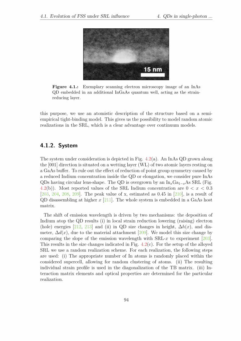
4.1. Evolution of FSS under SRL influence 4. QDs in single-photon ...
Figure 4.1.: Exemplary scanning electron microscopy image of an InAsQD embedded in an additional InGaAs quantum well, acting as the strain-reducing layer.
this purpose, we use an atomistic description of the structure based on a semi-empirical tight-binding model. This gives us the possibility to model random atomicrealizations in the SRL, which is a clear advantage over continuum models.
4.1.2. System
The system under consideration is depicted in Fig. 4.2(a). An InAs QD grown alongthe [001] direction is situated on a wetting layer (WL) of two atomic layers resting ona GaAs buffer. To rule out the effect of reduction of point group symmetry caused bya reduced Indium concentration inside the QD or elongation, we consider pure InAsQDs having circular lens-shape. The QD is overgrown by an InxGa1−xAs SRL (Fig.4.2(b)). Most reported values of the SRL Indium concentration are 0 < x < 0.3[203, 204, 208, 209]. The peak value of x, estimated as 0.45 in [210], is a result ofQD disassembling at higher x [211]. The whole system is embedded in a GaAs hostmatrix.
The shift of emission wavelength is driven by two mechanisms: the deposition ofIndium atop the QD results (i) in local strain reduction lowering (raising) electron(hole) energies [212, 213] and (ii) in QD size changes in height, Δh(x), and dia-meter, Δd(x), due to the material attachment [209]. We model this size change bycomparing the slope of the emission wavelength with SRL-x to experiment [203].This results in the size changes indicated in Fig. 4.2(c). For the setup of the alloyedSRL we use a random realization scheme. For each realization, the following stepsare used: (i) The appropriate number of In atoms is randomly placed within theconsidered supercell, allowing for random clustering of atoms. (ii) The resultingindividual strain profile is used in the diagonalization of the TB matrix. (iii) In-teraction matrix elements and optical properties are determined for the particularrealization.
94

4. QDs in single-photon ... 4.1. Evolution of FSS under SRL influence
Figure 4.2.: (a) System without SRL, consisting of an InAs QD on anInAs WL embedded in a GaAs host matrix. (b) System for nonzero SRL-xexaggerating size change for illustration reasons. (c) QD size changes withSRL Indium concentration reproducing the experimental emission wavelengthslope from [203] and resulting change in aspect ratio (AR) for QD3.
In our calculations for the excitonic FSS we employ our NN sp3s∗-TB model withthe parametrization from Ref. [107] and a valence-band offset between InAs andGaAs of 0.05 meV [214]. Strain-relaxation with the Keating potential is carried oututilizing the implementation from Ref. [61]. For the scaling with strain we use thevalue of η = 2.9 for all off-diagonal matrix elements, as suggested in Ref. [77].
4.1.3. Results and discussion
Calculations of the emission wavelength were performed for a fixed QD diameter of15.82 nm and four different QD heights: 1.13 nm (QD1), 1.69 nm (QD2), 2.26 nm(QD3) and 3.39 nm (QD4). Both diameter and height are subject to a linear increasewith SRL-x due to additional material deposition. We benchmark the slope of thegroundstate emission wavelength with SRL-x with experimental data from Ref. [203],resulting in the size changes shown in Fig. 4.2(c). Fig. 4.3 shows the increase of theemission wavelength with SRL-x. QD1 provides a good match with the experimentaldata. For comparison, results for QD2 without any QD size increase are shown inFig. 4.3, covering the strain-induced shift in emission wavelength alone, resulting ina much smaller slope (dashed line).
95

4.1. Evolution of FSS under SRL influence 4. QDs in single-photon ...
0 5 10 15 20 25 30
SRL Indium concentration [%]
1.0
1.2
1.4
1.6
Em
issi
on
wav
elen
gth
[μm
]
QD2 (strain shift only)
Experiment
QD4
QD3
QD2
QD1
Figure 4.3.: Shift of excitonic emission wavelength with SRL Indium con-centration for QDs of different height. Comparison with experimental valuesand with QDs lacking size increase.
The shift of emission wavelength with SRL-x desired for long-wavelength commu-nication is reproduced, reaching the value of 1.53 μm for the largest QDs covered byan In0.3Ga0.7As SRL driven by both strain relieve and additional material deposition.
The trend of increasing emission wavelength with increasing height at a fixed valueof SRL-x can be understood in a simple particle-in-a-box picture, where the QD-height corresponds to the box-width. Enlarging the width causes the electron (hole)energy levels to drop (raise), reducing the recombination energy.
Having benchmarked our model with the experimental data we calculate the FSSfor the considered QDs. Even without a SRL, the FSS exhibits statistical fluctu-ations due to symmetry reduction by QD structure and composition fluctuationsand resulting individual strain profiles [215, 216]. With the SRL present, the sym-metry is further reduced by the statistical distribution of atoms in the InxGa1−xAsalloy. In Fig. 4.4 the statistical fluctuation of the calculated FSS with the emissionwavelength is shown.
All calculated values of the FSS spread between the smallest calculated value of6 μeV and 119 μeV, which is in very good agreement with experiments for InAsQDs [126, 203, 204]. A general trend of increasing FSS with increasing emissionwavelength can be seen in Fig. 4.4 and is consistent with experimental and theoreticaltrends for both single QDs and SRL samples [126, 217–219]. A linear fit is providedas a guide to the eye.
In Fig. 4.5 the variation of the FSS with SRL-x is shown for the four different QDs.For each QD-height/SRL-x combination five realizations were averaged, giving the
96

4. QDs in single-photon ... 4.1. Evolution of FSS under SRL influence
1.0 1.1 1.2 1.3 1.4 1.5 1.6
Emission wavelength [μm]
0
25
50
75
100
125
FS
S[μ
eV]
Linear fitCalculated FSS
Figure 4.4.: Statistical scattering of the calculated FSS with excitonic emis-sion wavelength and linear fit.
depicted data. Error bars show the standard deviation of the FSS for each datapoint. For small SRL-x, all QDs show an increase of the FSS. From an intuitivepoint of view the initial increase in FSS can be understood by symmetry loweringvia the inclusion of Indium atoms in the SRL, but in this picture the increase withSRL-x should carry on over the whole range of x, resulting in an overall increaseof FSS. The initial increase is continued for QD1 until high SRL-x values, wheresaturation can be seen. For the larger QDs (QD2–QD4) at small SRL-x already areduction of the FSS is calculated. The data suggests a trend that in larger QDs thepossible reduction of the FSS occurs already at lower In concentrations. For largeSRL-x of 0.3, the FSS for all QDs tends to take intermediate values in the range of45±15 μeV.
With these results we demonstrate that utilizing a SRL for wavelength-shiftingdoes not compromise the applicability of QD-SRL samples by unintentionally raisingthe FSS. Moreover, for some geometries the FSS is even reduced, maintaining thepossibility of post-growth minimization of FSS.
Following the argumentation of Ref. [219], a reduction of the FSS is caused bya delocalization of electronic wave functions. We demonstrate that growing anSRL on the QD can lower the FSS due to the same reasons: the SRL weakens theconfinement potential in growth direction, leading to a small spread of wave functioninto the SRL region and a reduction of the electron-hole exchange matrix element.
97

4.1. Evolution of FSS under SRL influence 4. QDs in single-photon ...
0 5 10 15 20 25 30
SRL Indium concentration [%]
0
20
40
60
80
100
FS
S[μ
eV]
QD4
QD3
QD2
QD1
Figure 4.5.: Variation of the FSS as a function of SRL Indium concentrationfor different QD height from averaging over FSSs for each QD height andSRL-x. The initial increase in FSS for all QDs in regions of small SRL-xis counteracted by a reduction for larger SRL-x. A convergence of FSS tomediate values of around 45μeV can be seen.
Simultaneously, the recombination energy of the exciton is decreased due to largerQD-size with SRL-x and the modified strain profile. This effect seems to overtakethe effect of symmetry lowering the earlier, the larger the QD height.
For device integration the emission efficiency is an important quantity. In Fig.4.6 we show the squared dipole matrix element of the excitonic transition with po-larization along [110] crystal direction DX([110])2, plotted versus the SRL Indiumconcentration. It can be observed, that both increasing the QD height or the SRL-xstrengthens the excitonic dipole transition, which is beneficial for device applica-tions.
In conclusion, we have presented tight-binding and CI calculations of the FSS inInAs/GaAs QDs emitting at telecom wavelengths suited for long-range quantumcommunication. Our data emphasizes the possible use of the QD-SRL system fordevice application because operation at telecom wavelengths can be reached whileexcitonic transitions are strengthened with SRL-x. Counterintuitively, the FSS doesnot increase persistantly, but shows reduction and saturation, making the systemfeasible for the generation of entangled photon pairs.
98

4. QDs in single-photon ... 4.2. Optical gain in QD active media
0 5 10 15 20 25 30
SRL Indium concentration [%]
3
4
5
6
7
8
DX
([1
10
])2
(arb
.u.) QD4
QD3
QD2
QD1
Figure 4.6.: Plot of squared excitonic dipole transition matrix elementversus the SRL Indium concentration for QD1-QD4. With larger QD heightand with larger SRL-x transitions become more efficient.
4.2. Optical gain in QD active media
Now we turn to a different property of QD emitters: the optical gain in the presenceof excited carriers residing in the QD and WL states [220]. The saturation beha-viour of optical gain with increasing excitation density is an important factor forlaser device performance. For active materials based on self-organized InGaAs/GaAsquantum dots we study the interplay between structural properties of the quantumdots and many-body effects of excited carriers in the optical properties via a com-bination of tight-binding and quantum-kinetic calculations in this section. In thissection we first introduce the optical gain, the envelope approximation and the fit-ting procedure of TB wave functions onto their analytical envelope counterparts.Then we link these wave functions with quantum-kinetic calculation of the opticalgain spectra.
4.2.1. Optical gain
We employ a quantum-kinetic theory for the optical gain, that accounts for non-Markovian effects and self-consistent QD energy renormalizations. The calculationsare based on the semiconductor Bloch equation (SBE, [221]) for the interband trans-ition amplitudes ψα = 〈eαhα〉, which are formulated in the frequency domain [222]
(�ω − εe,HFα − εh,HF
α )ψα(ω) +[1 − f e
α − fhα
]ΩHF
α (ω)= Sc
α(ω) + Spα(ω) .
(4.1)
99

4.2. Optical gain in QD active media 4. QDs in single-photon ...
The single-particle energies εa,HFα = ea
α +Σa,HFα with a = e, h contain the TB energies
eaα and Σa,HF
α = ∑β (Vαββα − Vαβαβ) fa
β combines the Hartree and exchange Coulombself-energy. The Coulomb exchange contributions to the interband Rabi energyΩHF
α (ω) = d · E(ω) + ∑β Vαβαβψβ(ω) give rise to the excitonic resonance of the WL
and to excitonic renormalizations of the QD transitions. Additionally, Scα(ω) and
Spα(ω) describe the carrier-carrier and carrier-phonon correlations, that are evaluated
in the Born approximation and random-phase approximation, respectively [223].These lead to interaction-induced dephasing of the interband transition amplitudesψα in the time domain, which results in line-broadening as well as additional lineshifts in the frequency domain. Because of the discrete energy level structure inQD systems, two factors complicate the numerical evaluation. First, memory effectsare non-negligible, so that the Markov approximation should no longer be used[222]. As described above, we circumvent this problem by evaluating the SBE andcorrelation integrals in the frequency domain, and it is the frequency dependenceof the correlation contributions Sc
α(ω) and Spα(ω) that is expression of the non-
Markovian memory effects [222]. Moreover, it is important to properly evaluate thescattering integrals by using self-consistently renormalized energies rather than thefree single-particle energies.
Both carrier-phonon interaction using the polaron picture and carrier-carrier in-teraction can be cast into the form
Sc,pα (ω) = − ΓDD
α (ω)ψα(ω) +∑
β
ΓODαβ (ω)ψβ(ω) . (4.2)
One can identify contributions which are diagonal in the state index α (s, p, or WL)for the transition amplitude (diagonal dephasing ΓDD) and off-diagonal parts (ΓOD)which connect the interband transition amplitudes for various states.
We consider the linear optical response to a weak probe field E, and use for f e(h)α
Fermi-Dirac functions with total carrier densities
N = 2Ndot
∑α
f e(h)α + 2A−1 ∑
k
fe(h)k . (4.3)
In all examples, a temperature of 300 K is assumed. In the above equation, Ndot
is the 2-dimensional QD density and A is the active layer area. The solution toEq. (4.1) provides the intrinsic material gain.
4.2.2. Envelope approximation
In Ref. [224] it has been shown that for lens-shaped QDs with small height todiameter ratio, the wave functions separate in good approximation into in-planeand z-components. We utilize this property by mapping the full three-dimensional
100

4. QDs in single-photon ... 4.2. Optical gain in QD active media
wave functions from the TB calculation onto analytical counterparts for the in-plane and z-components to determine the interaction matrix elements as describedin [223]. This way we connect the many-body gain calculation to realistic QD sizeand composition properties.
Simple but widely used models for the calculation of electron and hole bound statesin semiconductor nanostructures are based on the envelope approximation, in closeconnection to the effective mass approximation [225]. Following the discussion in[226], in the envelope approximation the n-th bound wave function in a semicon-ductor nanostructure is represented by the product of a slowly oscillating envelopepart fn(r) and a fast oscillating part u0(r):
ψn(r) = fn(r)u0(r). (4.4)
Here, u0(r) is the Bloch function for k = 0 that oscillates with the lattice periodicity.It can be shown for quantum wells, that the envelope function fn(r) factorizes intoa part along the growth axis (z-axis) and a perpendicular part:
fn(ρ, z) = φ(ρ)χn(z) (4.5)
where ρ and z give the position in cylindrical coordinates. This factorization hasbeen shown to hold even for flat quantum dots with small height to diameter ratioin [224]. The in-plane part φ(ρ) can be described by a plane wave due to thetranslational symmetry troughout the quantum well. The actual form of the functionχn(z) depends on the choice of model for the quantum well. For analytical solutions,the quantum well is modelled as a potential well in z-direction with either infiniteor finite height, ranging from −L
2 to L2 . Here, L is the quantum well extension in
growth direction. For the infinite well the lowest bound state is given by
χinf1 (z) =
√2L
cos(
π
Lz)
. (4.6)
As shown in Fig. 4.7 the infinite potential well is a rather bad choice becausequantum mechanical wave functions penetrate into the barrier material. The infinitepotential well does not account for this behaviour. For a potential well of finite heightthe lowest bound state is given by
χfin1 (z) = α
⎧⎪⎪⎪⎨⎪⎪⎪⎩
exp(κz), for − ∞ < z ≤ −L2
exp(−κL/2)exp(kL/2) cos(kz), for − L
2 < z < L2
exp(−κz), for L2 ≤ z < ∞.
(4.7)
The prefactor α is given by
α = ekL/2[(
1 + κ2
k2
)(L
2 + 1κ
)]− 12
, (4.8)
101

4.2. Optical gain in QD active media 4. QDs in single-photon ...
-8 -6 -4 -2 0 2 4 6 8Growth direction [nm]
Env
elop
e am
plitu
de
Fit via finite potential wellFit via infinite potential wellElectron ground state envelope
Figure 4.7.: Comparison between the models of infinite and finite height ofthe potential well in envelope function approximation for the standard lens-shaped QD of the previous sections. Due to the penetration of the envelopewave function into the buffer the infinite potential well is not suited for fittingthe envelope functions accurately.
with k and κ obeyingk · tan
(k
L
2
)= κ. (4.9)
As shown in Fig. 4.7, this is a more realistic description of the wave function inz-direction, as intuitively understood.
Turning to quantum dots, this model has been used for the calculation of electronicstates of flat dots with rotational symmetry. In growth direction it appears naturalto see the dot as a quantum well, but this picture is spoiled for the in-plane part. Inthe ρ-plane the wave functions φ(ρ) cannot be described by plane waves because theconfinement degrades the translational symmetry. They can rather be approximatedby the eigenfunctions of a quantum harmonic oscillator [220, 227]. For this modelthe ground state is given by a gaussian envelope
φs(ρ − R) = β√π
e− β22 |ρ−R|2 , (4.10)
where R denotes the center of the quantum dot in the ρ-plane. The parameter β isreferred to as the inverse oscillator length:
β =√
mΔE
�. (4.11)
102

4. QDs in single-photon ... 4.2. Optical gain in QD active media
The factor ΔE accounts for the equidistant energy splitting in the quantum har-monic oscillator model and � is Planck’s constant.
4.2.3. Realistic envelopes
On the one hand we are able to calculate the atomistic single-particle wave functionsby means of our tight-binding model on a very involved level. On the other hand forsubsequent calculations, e.g. solving for the density matrix time evolution includingreservoirs or quantum-kinetic calculations, the envelope function model is the onlychance to include single-particle properties in the calculation: due to the problemsize the wave functions can only be dealt with properly via the factorization intoin-plane and z-parts. To steer a middle course and use at least the best parametersavailable for the envelope function approximation, we fit the functions φs(ρ − R)and χfin
1 (z) of Eqns. (4.10) and (4.7), respectively, to the full three-dimensionaltight-binding wave functions. Doing so, we integrate the wave functions over aperpendicular spatial direction as shown exemplarily in Fig. 4.8. For a fit of the
Figure 4.8.: Visualization of the fits in growth direction for the gain cal-culations. The lower part shows the ground hole wave function of QD 2 inside-view, integrated along [010]. In the upper part an exemplary envelopefit is shown. The fitting is done with respect to the yellow line, i.e. along thegrowth direction and through the quantum dot center.
z-part ([001]) we integrate over ρ and use k and L as fitting targets. For the fit of
103

4.2. Optical gain in QD active media 4. QDs in single-photon ...
the ρ-part we integrate over x ([100]) or y ([010]) to account for the QD shape fromtwo different sides and use the inverse oscillator length β as the fitting target. Toaccount for the three-dimensional structure of the QD we average the fitting resultsfor the x- and y-directions. The obtained fitting parameters are shown in Tab. 4.1for two realistic quantum dots having lens-shape, mean Indium concentrations of30% and 40% and a height and diameter of 2.2 nm and 25 nm (QD 1) and 2.0 nmand 15 nm (QD 2), respectively.
0 5 10 15 20 25 30 35[100] crystal direction [nm]
Env
elop
e am
plitu
de
Electron ground state envelope (TB)Hole ground state envelope (TB)Fitted electron ground state envelopeFitted hole ground state envelope
Figure 4.9.: [100]-dependence of the envelopes of the wave functions as cal-culated by TB for the ground states of electrons and holes, respectively, aswell as their fitted analytical counterparts. QD 2 as defined in the text wasused. Due to the reduced Indium content in the quantum dot, wave functionsspread layerwise.
A few trends appear intuitively: Modelling the quantum confinement in growthdirection as a quantum well and in the perpendicular plane as a harmonic oscillatorpotential is a better choice the higher the Indium content of the QD is. For a pureQD, the dot appears as a quantum well when seen only in a small region of a fewnm. For QDs with low Indium content the actual atomic realization becomes moreimportant and spoils the envelope function approximation, as shown in Figs. 4.9and 4.10. Here, a QD having lens-shape with height and diameter of 2,0 and 15nm, respectively, being composed of In0.4Ga0.6As, was used. For a pure InAs-QD asin Fig. 4.7 the envelope function approximation is quite good for electrons, as canbe seen in comparison with the results of section 2.7, where the nearly equidistantenergy spacing of bound electron states was observed. For holes, nevertheless, theenergies never appear in such an equidistant alignment. Therefore the obtained fitis worse for holes than for electrons. Often it is assumed for electrons and holes tohave equal envelopes, although not implied by the envelope function definition or
104

4. QDs in single-photon ... 4.2. Optical gain in QD active media
0 5 10 15 20 25 30 35[010] crystal direction [nm]
Env
elop
e am
plitu
de
Electron ground astate envelope (TB)Hole ground state envelope (TB)Fitted electron ground state envelopeFitted hole ground state envelope
Figure 4.10.: [010]-dependence of the envelopes of the wave functions ascalculated by TB for the ground states of electrons and holes, respectively, aswell as their fitted analytical counterparts. QD 2 as defined in the text wasused. Due to the reduced Indium content in the quantum dot, wave functionsspread layerwise.
-8 -6 -4 -2 0 2 4 6 8[001] crystal direction [nm]
Env
elop
e am
plitu
de
Electron ground state envelope (TB)Hole ground state envelope (TB)Fitted electron ground state envelopeFitted hole ground state envelope
Figure 4.11.: [001]-dependence of the envelopes of the wave functions ascalculated by TB for the ground states of electrons and holes, respectively,as well as their fitted analytical counterparts. QD 2 as defined in the textwas used. The asymmetry of wave functions is caused by the influence of thewetting layer.
105

4.2. Optical gain in QD active media 4. QDs in single-photon ...
QD ke Le βe kh Lh βh
1 0.,725 1.691 0.275 1.049 1.262 0.2602 0.,806 1.502 0.343 1.068 1.411 0.336
Table 4.1.: Fitted values for factor k, the well width L and inverse oscillatorlength β for both electrons and holes.
the calculated tight-binding wave functions. The differences of the electron and holewave function envelopes can be seen in Figs. 4.9 to 4.11.
0 20 40 60 80 100QD Indium content [%]
0
0,5
1
1,5
Dis
tanc
e of
WL
to g
roun
d st
ate
enve
lope
max
ima
[nm
]
ElectronsHoles
Figure 4.12.: Spatial distances in growth direction ([001]) of the center ofelectron and hole ground state envelope functions to the WL band edges as afunction of the QD Indium content. Increasing the carrier confinement due toincreased Indium content causes the wave function center to shift away fromthe wetting layer.
In the subsequent evaluations of scattering integrals entering the gain calculationsthe spatial distance in growth direction, i.e. the wave function overlap in [001]-direction, determines the scattering efficiency. We visualize in Fig. 4.12 the evolu-tion of this overlap as a function of the QD Indium content for QD 1. The spatialdistances are derived as the difference of the centers of the respective fitted envelopefunctions for electrons and holes to the centers of the WL electron and hole bandedges. As a general trend it can be seen, that because of the increasing confinementdue to the increasing QD Indium content, the QD envelope functions are drawnaway from the WL. Due to the different envelopes, this behaviour differs for elec-trons and holes, although the general trend holds. For hole envelope functions, thedistance appears smaller than for electron envelope functions due to the shallowerconfinement at the valence bands.
106

4. QDs in single-photon ... 4.2. Optical gain in QD active media
4.2.4. Negative differential gain in QD systems
Gain properties play a central role in the design and performance of optoelectronicdevices. For semiconductor active materials, the single-particle electronic statesare defined by structural properties such as material composition, quantum con-finement and strain. Optical properties are additionally influenced by many-bodyeffects of the excited carriers. The excitation dependence of the optical gain is de-termined by the interplay of phase-space filling, energy renormalization (e.g. gapshrinkage), dephasing, and screening of the Coulomb interaction. Of particularimportance for device applications is the saturation behavior of the optical gainwith increasing excitation density. For semiconductor quantum wells the excitationdependence of gain spectra is dominated by phase-state filling (PSF) and energyrenormalizations. Coulomb enhancement of interband transitions and homogeneousline broadening additionally contribute to magnitude and spectral distribution ofthe gain [221, 228–231]. Semiconductor QDs behave quite differently in this re-spect due to the presence of localized electronic states with discrete energies. Forsemiconductor QDs the gain saturation is predominantly influenced by the inter-play of PSF and excitation-induced dephasing (EID). Assuming quasi-equilibriumcarrier populations for the excited electrons and holes, state filling is gouverned bythe respective Fermi-functions. Naturally, the inversion of the lowest QD interbandtransition increases with excitation density and saturates when the correspondingstates are fully populated. EID is provided by carrier-carrier Coulomb scatteringand carrier-phonon scattering processes, which have been extensively studied in thepast for QD systems [177, 222, 232–236]. Part of the excited carriers reside in de-localized wetting-layer (WL) and barrier states being coupled to the QD states viascattering processes. Mostly due to the availability of additional scattering partners,EID also increases with excited carrier density [177]. The corresponding broadeningreduces the optical peak gain. As a result, two scenarios can occur. Usually PSFincreases faster than EID and the optical gain saturates for high excitation densities.In the other scenario, EID and the corresponding broadening of the QD resonancesincreases faster than the PSF, thus leading to a negative differential gain, i.e., areduction of the peak gain with increasing excitation density. This behavior hasbeen predicted theoretically [176, 237, 238] and was recently observed [239] usinggain spectra obtained via the Hakki-Paoli technique [240] at elevated temperatures.In what follows, we identify regimes in which the respective scenarios occur for real-istic QD structures and investigate the influence of structural properties on the gainsaturation.
We consider an ensemble of InGaAs QDs, taking into account the two lowest con-fined shells for electrons and holes, labeled s- and p-states, respectively, as well asthe quasi-continuum of WL states. Single-particle energies and wave functions ofthese lowest QD shells are extracted from atomistic tight-binding (TB) calculationsas discussed above in Chapter 2 using the sp3s∗-model with nearest neighbors and
107

4.2. Optical gain in QD active media 4. QDs in single-photon ...
spin-orbit coupling as well as including strain calculated via valence force field min-imization of the total strain energy. As described above, we link the results fromthe calculation of the single-particle properties to their analytical counterparts toenter the gain-calculation.
4.2.5. Results and discussion
To illustrate the emergence of the two aforementioned regimes of gain saturation, weinvestigate two exemplary QDs, each representing either dominant PSF or EID. QD1 is lens-shaped with diameter and height of 25 nm and 2.2 nm, respectively, beingcomposed of In0.3Ga0.7As. Excitation dependent optical gain spectra in Fig. 4.13exhibit the peak gain saturation with increasing excitation due to PSF, accompaniedby EID and a redshift of the s-shell absorption due to the Coulomb interaction ofQD and WL carriers. The calculated EID of the lowest QD transition saturates atelevated carrier densities and is even slightly reduced for 1 × 1012cm−2. It is thesaturation of the population inversion, which dominates the density dependence ofthe peak gain, except for the highest considered carrier density, where the reducedbroadening leads to a slightly increased peak gain.
-180 -170 -160 -150 -140E-E
G [meV]
-0.004
-0.002
0
0.002
0.004
abso
rptio
n [a
rb. u
nits
]
2e121e127e115e112e111e11
-150 -100 -50
-0.01
0
0.01
Figure 4.13.: Low-energy part of the optical spectra for QD 1 with 30%In content and various excitation densities (in cm−2) as a function of energyrelative to the WL energy gap EG. The inset shows optical spectra for lowand high excitation density covering s-shell, p-shell and the WL absorptionedge.
Small changes of the structural properties can significantly alter this behaviour,
108

4. QDs in single-photon ... 4.2. Optical gain in QD active media
as is demonstrated by our second example. QD 2 is lens-shaped with a diameterand height of 15 nm and 2.0 nm, respectively, being composed of In0.4Ga0.6As. Inthe excitation dependent optical gain spectra of Fig. 4.14, the dominant role ofdephasing can be identified, as the s-shell transition is strongly broadened withincreasing excitation density. As a result, only for weak excitation the peak gainincreases with carrier density. As soon as the EID increases faster than the inversion,the peak gain is reduced and the regime of negative differential gain is reached. Wenote that the increasing EID in a situation where the QD inversion saturates is adirect consequence of the electronically coupled 0D+2D (QD+WL) system.
-210 -200 -190 -180 -170 -160 -150 -140E-E
G [meV]
-0.003
-0.002
-0.001
0
abso
rptio
n [a
rb. u
nits
]
2e121e127e115e112e111e11
Figure 4.14.: Low-energy part of the optical spectra for QD 2 and 40%In content for various excitation densities (in cm−2) as a function of energyrelative to the WL energy gap.
To investigate the interplay between structural properties on the one hand andEID and PSF on the other, the carrier density dependence of the peak gain is shownin Fig. 4.15 for QD 1 (solid line), QD 2 (dashed line), as well as for the samegeometries and reduced Indium content. For QD 1 the peak gain slowly saturateswhile for QD 2 at elevated carrier densities a negative differential gain is obtained.If we lower the Indium content in QD 1 (dash-dotted line), the overall peak gainis reduced and the onset of saturation is shifted to higher carrier densities due toshallower confinement. For QD 2 a reduced Indium content (dotted line) leads to agradual disappearance of negative differential gain.
These rather involved dependencies can be understood from Fig. 4.16, where thespectral broadening (a) and the inversion (b) of the s-shell transition are shown.A substantial difference in the excitation dependence of the spectral broadening
109

4.2. Optical gain in QD active media 4. QDs in single-photon ...
1e+11 1e+12carrier density [cm
-2]
-0.004
-0.002
0
0.002
0.004
peak
gai
n [a
rb. u
nits
]
QD 1 (25%)QD 1 (30%)QD 2 (30%)QD 2 (40%)
Figure 4.15.: Excitation density dependence of the peak gain for selected QDgeometries, with given In content. QD 1 (30%) and QD 2 (40%) correspondto Figs. 4.13 and 4.14, respectively.
between QD 1 and QD 2 can be observed. In all cases, the broadening increases withcarrier density in a comparable way for low excitation densities. In QD 1 with 30%Indium content (solid line) the broadening saturates and is even reduced for largeexcitation densities due to a combination of QD single-particle shifts (increasing theenergetic distance of QD and WL scattering partners), state filling (leading to Pauliblocking of scattering channels), and screening (reducing the Coulomb interaction).In contrast, the broadening in QD 2 (dashed line) increases monotonously also in aregime where the inversion has already saturated, see Fig. 4.16 (b), thus leading tonegative differential gain.
For the regime of dominant dephasing, that depends on the dephasing increasingwith excitation density, we can identify a connection to structural properties. QD 1with 25% Indium content has the shallowest confinement and the strongest reductionof EID at high carrier densities. For QD 1 and 30% Indium content, the deeper QDconfinement reduces the dephasing itself and the density dependent quenching of thedephasing is less pronounced. QD 2 with 30% Indium content has an even deeperconfinement as QD 1 due to its reduced size. Here, no reduction of EID is observed,but only a saturation. Finally, QD 2 with 40% Indium content has the deepestconfinement and shows a monotonous increase of dephasing.
To provide further insight from the viewpoint of the microscopic calculation, we
110

4. QDs in single-photon ... 4.2. Optical gain in QD active media
1e+11 1e+12carrier density [cm
-2]
0
5
10sp
ectr
al b
road
enin
g [m
eV]
QD 1 (25%)QD 1 (30%)QD 2 (30%)QD 2 (40%)
1e+11 1e+12carrier density [cm
-2]
-1
-0.5
0
0.5
1
Inve
rsio
n
(a) (b)
Figure 4.16.: Excitation density dependence of s-shell broadening (a) andinversion (b) for various QD geometries and Indium contents.
compare in Fig. 4.17 the different diagonal and off-diagonal dephasing contributionsΓDD
α (ωp) and ΓODαβ (ωp) due to carrier-carrier scattering at peak gain energy �ωp. Quite
counterintuitively, both diagonal and off-diagonal s-shell dephasing components arereduced with increasing carrier density due to a combination of increased QD levelshifts and screening of the Coulomb interaction. However, the difference of bothcontributions increases with carrier density, and this determines the net diagonaldephasing, cf. Eq. (4.2). Additionally, in Fig. 4.17 we provide the ΓOD
sp -component,which is stronger for QD 2 than for QD 1. As a result of many-body compensationeffects, ΓOD
sp reduces the dephasing according to Eq. (4.2). Hence the reduction ofΓOD
sp with increasing carrier density leads to a net increase of the total dephasing.Since the role of ΓOD
sp is stronger in QD 2, the off-diagonal dephasing supports forQD 2 the prevailing dephasing regime.
In conclusion we can identify two regimes in which either excitation-induced de-phasing or phase-space filling dominates the evolution of the QD peak gain withexcitation density. It is shown that high Indium contents or small QD sizes leadto a faster saturation of the QD inversion. In this case, further increasing dephas-ing can result in negative differential gain. Moreover, smaller QDs show a differentdensity dependence of the ratio between diagonal and off-diagonal dephasing, alsofostering the dominant role of broadening in high-density gain spectra. These find-ings should support further experimental investigations or applications of negative
111
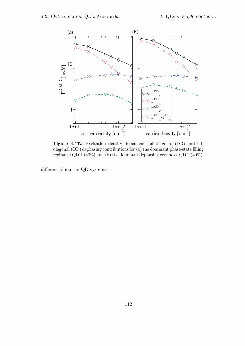
4.2. Optical gain in QD active media 4. QDs in single-photon ...
1e+11 1e+12carrier density [cm
-2]
1
10Γ
DD
,OD
[m
eV]
ΓDD
s
ΓOD
ss
ΓOD
sp
ΓDD
ss-Γ
OD
ss
1e+11 1e+12carrier density [cm
-2]
(a) (b)
Figure 4.17.: Excitation density dependence of diagonal (DD) and off-diagonal (OD) dephasing contributions for (a) the dominant phase-state fillingregime of QD 1 (30%) and (b) the dominant dephasing regime of QD 2 (40%).
differential gain in QD systems.
112

4. QDs in single-photon ... 4.3. Conclusion
4.3. Conclusion
Devices based on self-assembled InGaAs/GaAs quantum dots are close to market-ready, although some difficulties have to be circumvented. In the previous sectionsof this chapter we presented studies concerning some of these difficulties, guidingthe way towards self-organized QDs as optical components in device applications afew steps.
Concerning section 4.1, these devices include various light emitters for quantumcomputing and communication [241], ranging from LEDs at telecom wavelengthsfor conventional fiber transport of information to devices emitting polarization en-tangled photon pairs, such as quantum repeaters [242–244] for long-range fiber trans-port of information encrypted by protocols using entanglement-based schemes orwrite and read-out devices for generation of quantum keys for quantum key dis-tribution [245, 246]. Regarding the need for a vanishing fine-structure splitting,application of electromagnetic fields or combined external stresses as well as QD pre-selection are promising ways to minimize the FSS, as stated above. Nevertheless,for reliable fabrication of InGaAs QDs with vanishing FSS, growth-control-basedapproaches like growth af a SRL seem to be the best way to integrate QDs intodevices. In this respect, further research is needed optimizing the SRL influenceand FSS reduction at the same time. Recently, QDs in the InAs(P)/InP materialsystem have been shown to be promising candidates exhibiting smaller FSS and asmaller bandwidth of FSS with individual QD realizations [33, 216, 247].
In section 4.2 different regimes for the emergence of a negative differential gain inQD based active media were discussed. Those active media are to be integrated intonext generation LED and laser devices, where the different physical behaviour of QDscompared with QWs leads to the emergence of devices with superior performance[238, 248]. For these devices gain saturation behaviour with increasing excitationis important for the high-excitation regime, directly influencing the performance.Direct implementation of the negative differential gain effect could take place ingain-lever lasers [249, 250], allowing for new operational regimes, or in quantum dotoptical amplifiers [251]. Also, directly modulated lasers exhibiting a negative chirpcould be realized employing negative differential gain [252].
113


5. Summary and outlook

5. Summary and outlook
Summary
After an introduction into the vivid field of research on semiconductor quantumdots, we presented full details about the tight-binding theory for the calculationof electron and hole bound states and energies, respectively. We introduced thedifferences in modelling semiconductor bulk band structures and bound states innanostructures like quantum wells and quantum dots and, after introducing anddiscussing all relevant influences like spin-orbit coupling, strain and piezoelectricity,we presented a summary of common quantum dot structures from literature. Threetypical geometries and concentrations were identified and the corresponding single-particle energies and wave functions were presented as well as benchmarks for ournext-neighbour sp3s∗ tight-binding model. Subsequently we studied the influenceof the variation of QD height, diameter and Indium concentration on single-particleenergies and the fundamental energy gap. Attention was paid to the influence ofthe choice of the energy band alignment as expressed through the valence bandoffset between the two semiconductor materials and the number of bound stateswith respect to the QD geometry.
After this comprehensive introduction into single-particle tight-binding theory, wepresented the calculation of many-particle properties of charge carriers in QDs viathe configuration-interaction method. The derivation of Coulomb and dipole matrixelements from tight-binding coefficients was discussed as well as the subsequentcalculation of the excitonic emission and absorption spectra. Special attention waspaid to the excitonic fine-structure splitting of bright exciton states.
Based on this theoretical foundation we presented results of our calculations assummarized roughly in the following:
In section 4.1 we have shown tight-binding and configuration interaction calcula-tions of the excitonic fine-structure splitting in InAs/GaAs QDs emitting at telecomwavelengths suited for long-range quantum communication by means of overgrowthof the QD by a strain-reducing layer. Our data emphasizes the possible use of theQD-SRL system for device application because operation at telecom wavelengths canbe reached while excitonic transitions are strengthened with SRL-x. The depend-ence of the FSS on the SRL Indium content was derived by statistically averagingover different atomic realizations per SRL-x for different QD geometries. Slopesof the QD emission wavelength with SRL-x were calculated in excellent agreementwith experimental data by allowing for the QD size to rise due to additional mater-ial provided by the SRL. Counterintuitively, the FSS does not increase persistantly,but shows reduction and saturation, making the system feasible for the generationof entangled photon pairs.
In section 4.2 we examined the interplay of structural properties and many-body ef-fects on the optical gain spectra of active materials based on InGaAs/GaAs quantum
116
5. Summary and outlook
dots. For this we combined the single-particle energies and wave functions obtainedfrom our tight-binding model, which account for the structural QD properties, withquantum-kinetic calculations of the optical gain. We could identify two regimesin which either excitation-induced dephasing or phase-space filling dominates theevolution of the QD peak gain with excitation density. It was shown that high In-dium contents or small QD sizes lead to a faster saturation of the QD inversion.In this case, further increasing dephasing can result in negative differential gain.Moreover, smaller QDs show a different density dependence of the ratio betweendiagonal and off-diagonal dephasing, also fostering the dominant role of broadeningin high-density gain spectra. These findings should support further experimentalinvestigations or applications of negative differential gain in QD systems and willguide device design for semiconductor lasers.
Outlook
Technically, the utilized tight-binding model could be expanded in several ways tomake it more accurate or to integrate further physical aspects into the calculation.Depending on the desired application expanding the basis from sp3s∗ to sp3d5s∗ is anobvious expansion of the model. As mentioned earlier, this expanded basis is neededfor applications far away from the Γ-point, where the sp3s∗-basis fails to accuratelyreproduce the effective masses of the energy bands. If the ongoing discussion inthe tight-binding and pseudopotential community about the correct incorporationof piezoelectric effects comes to an end, this could be another improvement of themodel. Also, accounting for the effect of strain onto atomic orbitals (diagonal cor-rections in the TB Hamiltonian) could be beneficial. To paint an even more realisticpicture of epitaxially grown nanostructures, material segregation at boundary inter-faces between different materials, such as the boundary between QD and the bufferor the SRL and the buffer should be incorporated into the model via concentrationgradients. To enhance the agreement of optical spectra with experiments, dipolematrix elements could be calculated using orthogonalized Slater orbitals or usingexplicit basis functions obtained by DFT. From the latter, also TB parametriza-tions could be adopted to further increase the quality of the TB band structures.
Those expansions will not alter physical behaviour principally but allow for dif-ferent physical properties to investigate. From the physical point of view there arealso several possibilities for further work. For the evolution of the fine-structuresplitting with the Indium content of the strain-reducing layer, comparison to recentexperiments is intended. Indeed, finding a way to a systematical reduction of theFSS is necessary. Our results suggest that using the SRL geometry could be a pos-sible way, at least towards a fixed FSS, not a vanishing FSS. Also, varying the SRLstructure, i.e. the position of the SRL or the concentration gradients, will be worthstudying. A first step towards this direction will be using results of TEM, AFM and
117

5. Summary and outlook
PL measurements as inputs for the TB-modelling of the SRL-QD structures [253].
Besides further work on the topics presented in this thesis, research on other ma-terial systems, such as InAsP/InP would be of great interest. In the InAsP/InPmaterial system very small FSS was predicted [33] as well as QD emission at largewavelengths [247]. Also other applications of the TB model, for example to study QDmolecules (laterally or vertically coupled QDs) are possible. Here, the optical prop-erties are not only defined by the geometrical aspects but also by the distance of theQDs, which allows for tuning of the emission spectra with the distance between QDs.Interesting other systems are for example nanoplatelets, which are II-VI semicon-ductor plates with thickness of only a few monolayers and large lateral dimensions.Also, new thin-layered graphene-like materials such as MoS2 and other transitionchalcogenides appear interesting. Both nanoplatelets and thin-layered transition di-chalcogenides offer unique properties like large excitonic binding energies of up toseveral hundred meV.
However, due to the persistent trend of miniaturization, low-dimensional semicon-ductor structures with superior properties will proceed to conquer everyday opticaland electronic devices. With up-to-date and next generation computers, i.e. aslong as density functional theory can only allow for the inclusion of hundreds ofatoms in the calculations, the empirical tight-binding method for the description ofthe electronic and optical properties of these devices will be one of the methods ofchoice.
118

A. Appendix

A.1. Quantum dot growth A. Appendix
A.1. Quantum dot growth
In this section we give a short introduction to the epitaxial growth modes in whichsemiconductor quantum dots can be manufactured. For semiconductor heterostruc-tures, there are in general three common growth modes, as sketched in Fig. A.1differing mainly in the adhesion of provided atoms on a new grown layer in compar-ison to the bulk interface layer adhesion. With adhesion, the tendency of particlesof different kinds to cling to one another is meant. If the adhesion on the newsurface is similar to the bulk adhesion, the Frank-van-der-Merve-growth [254–256]takes place which leads to the consecutive growth of monolayers on top of eachother. If the adhesion on the new surface is much higher than the bulk adhesion,the so-called Volmer-Weber growth [257] happens, where due to the different adhe-sions high islands of the material to grow build up. In between these two extremalconditions, the Stranski-Krastanov growth [258] occurs, widely used for the fabric-ation of quantum dots. In the Stranski-Krastanov growth mode first one or a smallnumber of monolayers of the deposited material is built, called the wetting layer.After the buildup of a critical number of monolayers, islands formation on top of thewetting layer is favoured energetically due to strain from lattice mismatch. Thoseislands form the quantum dots.
Figure A.1.: Scheme of the different growth modes described in the text.Picture from [259].
There are two technical realizations of Stranski-Krastanov growth, called molecu-lar beam epitaxy (MBE) and metal organic vapor phase epitaxy (MOVPE). MBEgrowth is used to grow high quality quantum wells, wires and dots of different semi-conductor materials on top of a substrate located in ultra high vacuum. Materialsto grow are stored in effusion cells, which can be opened and closed to adjust therate of material flow, and are heated to form a molecular beam of material to adsorbat the surface of the substrate. With this technique of opening and closing shuttersfor effusion cells containing different materials complicated heterostructures can be
120

A. Appendix A.1. Quantum dot growth
formed, including monolayer growth, doping and overgrowth of structures. MBEgrowth can be controlled and monitored by in-situ diffraction techniques to probethe growing surface such as RHEED (reflection high energy electron diffraction).Due to requirement of ultra high vacuum and because of slow growth rates, MBEgrowth is relatively expensive.
In difference to MBE, in the MOVPE growth mode no vacuum is needed be-cause reactant materials (such as Trimethylgallium, Trimethylindium and Arsinefor InGaAs-heterostructures) are heated and pass the substrate in the vapor phaseat moderate pressure. Here, the growth does take place because of the chemical re-action of the vaporized materials with the substrate’s surface. This enables a fasterand cheaper growth of semiconductor heterostructures but produces less pure resultsthan using MBE growth. MOVPE has become the most used growth technique formass production of optoelectronic devices, especially for Nitride-based components.
121
A.2. LAMMPS best practice parameters A. Appendix
A.2. LAMMPS best practice parameters
Since no compendium for the choice of LAMMPS internal parameters is available,we report on the parameters used for the calculations in this thesis. We define thesize of the simulation box (supercell) via the xlo xhi (in x-direction) keywords inthe LAMMPS data file. We read out the values of the extremal atom positions andadd half a lattice constant aGaAs
2 of the host crystal at each interface to be able toaccount for the periodicity of the host crystal. To avoid artefacts, it turned out to befruitful to add an additional space of 10−5 nm at each side of the simulation domaindue to numerical reasons. In the LAMMPS input file for the minimization we usethe specifications units metal, atom style atomic and periodic boundary condi-tions via boundary p p p. It turned out, that for more symmetric problems, e.g.calculations with only a wetting layer in the supercell, the ’Hessian-free truncatedNewton’ (hftn) minimization method is the best choice (min style hftn). For thecalculations including a quantum dot with or without disorder, the ’conjugent gradi-ent’ (cg) method is the fastest and most robust algorithm for the minimization ofthe potential energy (min style cg). While using the conjugent gradient algorithmit is a good choice to reduce the ’step-size’ via min modify dmax 0.0005 to achievea robust computation. dmax limits the maximal spatial displacement of a singleatom in one iteration of the minimization and therefore acts as a damping in thesubsequent calculation steps. As a criterion for the minimization to terminate weuse an energy tolerance of etol = 1e−12 or a force norm tolerance of ftol = 1e−1,both being the difference between two consecutive steps in energy and the norm ofthe global force vector, respectively.
122

A. Appendix A.3. PETSc/SLEPc best practice parameters
A.3. PETSc/SLEPc best practice parameters
In PETSc, the environment for the solution of eigenvalue problems is called EPS(Eigenvalue Problem Solver). All optional arguments for the actual problem can bedefined as properties of this environment. For our standard calculations containinga diagonalization domain of around one million atoms and searching for a handfulof interior eigenpairs per electrons and holes, the following options turned out tosuit the problem best.The best solver for our quantum dot calculations turned out to be the Krylov Schuralgorithm which can be set via -eps type krylovschur. Find an overview overKrylov projection methods and the original references in [162].We set the diagonalization accuracy via -eps tol 1e-10 where the accuracy ismeasured relative to the eigenvalue:
eps tol!≤ ||Ax − kx||
||kx|| . (A.1)
A is the matrix to be diagonalized, k the approximate eigenvalue and x the approxi-mate eigenstate. The value of 1e-10 is needed for the calculation to converge tothe physically correct twofold Kramers degeneracy of the eigenstates due to spindegeneracy. For lower values, the computational time is shorter but p- and d-likestates show no degeneracy; although of course the eigenvalues differ only by a smallfraction. For a quick diagonalization in search of only the energy levels a toleranceof 1e-5 is enough, but if one wants to calculate optical properties via CI the de-generacies have to be taken into account in order to resolve fine-structure splittingsand polarization anisotropy.
As pointed out we are interested in highly accurate results, so we set the number ofmaximum iterations to a very large value via -eps max it 20000000. To acceleratethe computation we provide some basic mathematical properties of the matrix tothe solver: the TB-Hamiltonian matrix is hermitian -eps hermitian and thereforehas real eigenvalues. -eps target real sets the eigenvalue search to happen alongthe real axis only.
The number of eigenpairs to be computed can be set via -eps nev N where eachstate is counted individually, so choosing N = 2 will give the two s-like states andso on.
To calculate eigenpairs in the interior of the spectrum, as it is needed here becauseonly eigenpairs around the band gap are of interest, we choose the computation tosearch for eigenpairs closest to a target value via: -eps target 1.0. The value is ineV and should be as close as possible to the actual eigenvalues for fast convergence.
To further improve the convergence speed it turned out useful to use the harmonic
123

A.3. PETSc/SLEPc best practice parameters A. Appendix
Ritz extraction algorithm: -eps harmonic. This changes how the spectral inform-ation gets extracted from the single subspaces built from the original matrix in thediagonalization process. The maximum dimension of these subspaces to be used bythe solver can be set by using: -eps ncv 100. The fixed value of 100 turned outto be a good value for nev≈10. For monitoring the progress of these computationswe use -eps monitor for the convergence steps and -eps view for a printout of allproperties of the eigenproblem solver object. A typical output of -eps view lookslike
0: EPS Object:0: problem type: hermitian eigenvalue problem0: method: krylovschur0: extraction type: harmonic Ritz0: selected portion of the spectrum: closest to target: 1+0i (alongthe real axis)0: number of eigenvalues (nev): 80: number of column vectors (ncv): 1000: maximum dimension of projected problem (mpd): 1000: maximum number of iterations: 200000000: tolerance: 1e-100: convergence test: relative to the eigenvalue0: estimates of matrix norms (constant): norm(A)=10: IP Object:0: orthogonalization method: classical Gram-Schmidt0: orthogonalization refinement: if needed (eta: 0.707100)0: ST Object:0: type: shift0: shift: 0+0 i0: Elapsed Time: 5941.1537490: Number of iterations of the method: 830: Solution method: krylovschur0:0: Number of requested eigenvalues: 80: Stopping condition: tol=1e-10, maxit=200000000: Number of converged approximate eigenpairs: 90:0: k ||Ax-kx||/||kx||0: --------------------- ------------------0: 1.1192190630 +0.0000000000 i 2.53797e-110: 1.1192190630 +0.0000000000 i 8.39935e-110: 1.1926452383 -0.0000000000 i 4.63115e-110: 1.1926452383 -0.0000000000 i 2.07435e-110: 1.1994611374 -0.0000000000 i 6.69836e-11
124

A. Appendix A.3. PETSc/SLEPc best practice parameters
0: 1.1994611374 -0.0000000000 i 1.31763e-110: 1.2660478656 -0.0000000000 i 7.9943e-110: 1.2660478656 +0.0000000000 i 3.44358e-120: 1.2695011837 +0.0000000000 i 2.66525e-11
Although in general when dealing with large matrices not conditioned in particulara preconditioner should help accelerating the diagonalization process, in our caseall preconditioners turned out to be very memory demanding and slow in termsof convergence. Therefore no preconditioners where applied to the Hamiltonianmatrices throughout the calculations presented in this thesis.
125

A.4. TB parametrizations A. Appendix
A.4. TB parametrizations
In our quantum dot model using a next-neighbour sp3s∗ model including spin-orbitcoupling we use the band structure parametrization from [107]. The given paramet-ers reproduce low temperature bulk band gaps at the Γ-point of 1,511 eV for GaAsand 0,4152 eV for InAs, respectively. The literature values for these band gaps are1,519 eV for bulk GaAs and 0,415 eV for bulk InAs, respectively, at low temperatures[118]. In the literature there are many tight-binding parametrizations present, dif-fering in basis, number of neighbours considered, temperature dependence of targetvalues and physical purpose, i.e. optical properties or electronic transport. A goodoverview of parametrizations can be found in [48]. Selected parametrizations forGaAs and InAs in the next neighbour spin-orbit sp3s∗ model as used in this thesisare reported in Tab. A.1.
Using the variety of parametrizations we can choose the appropriate parametriza-tion for experiments with different temperatures. The evolution of the single-particleband gap with temperature is nonlinear and can be described by [118]
EGaAsGap (T ) = 1.519 − 5.405 · 10−4 T 2
(T + 204) (A.2)
EInAsGap (T ) = 0.415 − 2.760 · 10−4 T 2
(T + 83) . (A.3)
The formula provides the temperature dependent values of the band gap as shownin Tab. A.2 to compare the results employing the different TB-parametrizationagainst. Because of the small gradient of the single-particle band gap at smalltemperatures in both InAs and GaAs, the 77 K-parametrization still is suitable forlow temperature calculations because the band gap values differ only in the orderof meV to the 0 K case.
126

A. Appendix A.4. TB parametrizations
Wei et al. [107] Priester et al. [108] Klimeck et al. [106]T [K] 77 300 300
GaAs InAs GaAs InAs GaAs InAsEGap 1.511 0.4152 1.5499 0.429 1.424 0.3868EsA -9.2664 -9.3562 -8.3431 -9.5381 -3.53284 -9.21537EsC -4.3504 -3.9611 -2.6569 -2.7219 -8.11499 -2.21525EpA +1.4866 +1.8201 +0.9252 +0.7733 +0.27772 +0.02402EpC +3.2136 +3.1842 +3.5523 +3.5834 +4.57341 +4.64241Es∗A +8.7826 +7.0432 +7.4249 +7.2730 +12.3393 +7.44461Es∗C +5.8765 +6.1232 +6.6235 +6.6095 +4.31241 +4.12648VsAsC -7.9480 -6.5393 -6.4513 -5.6052 -6.87653 -5.06858VsAxC +2.7777 +4.3607 +4.4607 +3.0205 +2.85929 +2.51793VxAsC +10.005 +7.0849 +5.7413 +5.3894 +11.09774 +6.18038Vs∗AxC +3.6271 +3.0007 +4.3083 +3.2191 +6.31619 +3.79662VxAs∗C +7.0071 +5.4020 +6.6473 +3.7234 +5.02335 +2.45537VxAxC +2.3069 +2.5491 +1.9546 +1.8398 +1.33572 +0.84908VxAyC +5.0305 +5.4700 +5.0178 +4.3977 +5.07596 +4.68538ΔA +0.420 +0.420 +0.4014 +0.4155 +0.32703 +0.38159ΔC +0.174 +0.393 +0.1659 +0.387 +0.12000 +0.37518
Table A.1.: Material parameters for GaAs and InAs. The temperature de-notes at which temperature the band structure was fitted. EGap gives thesingle-particle gap calculated using the actual parametrization. E are theorbital energies, V are the hopping matrix elements, s, s∗ denote the s ands∗ orbitals while x and y are abbreviations for the px and py orbitals. Aand C denote anion and cation sites, respectively. ΔA/C corresponds to thespin-orbit-splitting parameters via ΔA/C = 3λA/C . All parameters are givenin eV unless stated otherwise.
GaAs InAs0 K 1.519 0.41577 K 1.5075 0.4047300 K 1.4224 0.354
Table A.2.: Single-particle bulk band gaps in eV at selected temperaturesfor InAs and GaAs.
127


Publications and conferencecontributions

Publications and conference contributions
Parts of this work have been published in journals:
• Negative differential gain in quantum dot systems: Interplay of structural prop-erties and many-body effectsApplied Physics Letters, 104, 24, 242108 (2014)Elias Goldmann, Michael Lorke, Thomas Frauenheim, and Frank Jahnke
• Excitonic fine-structure splitting in telecom-wavelength InAs/GaAs quantumdots: Statistical distribution and height-dependenceApplied Physics Letters, 103, 24, 242102 (2013)Elias Goldmann, Stefan Barthel, Matthias Florian, Kolja Schuh, and FrankJahnke
• Structural and emission properties of MOVPE-grown InGaAs/GaAs telecomquantum dots with bimodal height distributionSubmitted to Applied Physics Letters (2014)Elias Goldmann, Matthias Paul, Florian Krause, Jan Kettler, Thorsten Mehr-tens, Knut Muller, Andreas Rosenauer, Michael Jetter, Peter Michler, andFrank Jahnke
130

Publications and conference contributions
Parts of this work have been presented as talks and posters at conferences:
• Structural analysis, wavelength engineering and excitonic fine-structure split-ting in telecom quantum dots as quantum light emittersBMBF Q.com status seminar I, Bad Honnef (2014)Elias Goldmann, Stefan Barthel, Matthias Florian, Kolja Schuh, Frank Jahnke,Matthias Paul, Michael Jetter, Peter Michler, Florian Krause, Knut Muller,and Andreas Rosenauer
• Structure and optical properties of InGaAs telecom quantum dotsSolid state seminary, Bremen (2014)Elias Goldmann, Matthias Paul, Knut Muller, and Frank Jahnke
• Atom-by-atom modeling of QDsSolid-state workshop University of Bremen, Bad Bederkesa (2013)Elias Goldmann and Frank Jahnke
• Tight-binding model of strain-reducing layers in semiconductor quantum dotsDPG spring meeting condensed matter section, Berlin (2012)Elias Goldmann, Stefan Barthel, Kolja Schuh, Gerd Czycholl, and FrankJahnke
• Tight-binding model of strain-reducing layers in semiconductor quantum dotsBMBF Quantum Repeater status seminar II, Bad Honnef (2012)Elias Goldmann, Stefan Barthel, Kolja Schuh, Gerd Czycholl, and FrankJahnke
• The Single QD laser - From Weak To High ExcitationFOPS at Lake Junaluska, North Carolina, USA (2011)Christopher Gies, Matthias Florian, Paul Gartner, Elias Goldmann, AlexanderSteinhoff, Kolja Schuh und Frank Jahnke,
• Atomistic tight-binding models of semiconductor quantum dotsDPG spring meeting condensed matter section, Dresden (2011):Elias Goldmann, Stefan Barthel, and Frank Jahnke
131

Bibliography
[1] Katherine Sanderson. Quantum dots go large. Nature, 459(7248):760, 2009.
[2] R. Dingle, W. Wiegmann, and C. Henry. Quantum states of confined carriersin very thin AlxGa1−xAs-GaAs-AlxGa1−xAs heterostructures. Physical ReviewLetters, 33(14):827, 1974.
[3] A. I. Ekimov and A. A. Onushchenko. Size quantization of the electron energyspectrum in a microscopic semiconductor crystal. JETP Letters, 40(8):1136–1139, 1984.
[4] C. Murray, D. J. Norris, and M. G. Bawendi. Synthesis and characterizationof nearly monodisperse CdE (E= sulfur, selenium, tellurium) semiconductornanocrystallites. Journal of the American Chemical Society, 115(19):8706–8715, 1993.
[5] A. Luque, A. Marti, and C. Stanley. Understanding intermediate-band solarcells. Nature Photonics, 6, 2012.
[6] K. Bourzac. Quantum dots go on display. Nature, 493(7432):283–283, 2013.
[7] F. Meinardi, A. Colombo, K. A. Velizhanin, R. Simonutti, M. Lorenzon,L. Beverina, R. Viswanatha, V. I. Klimov, and S. Brovelli. Large-area lu-minescent solar concentrators based on “Stokes-shift-engineered” nanocrys-tals in a mass-polymerized PMMA matrix. Nature Photonics, Advance onlinepublication:1749–4893, 2014.
[8] X. Gao, Y. Cui, R. M. Levenson, L. W. K. Chung, and S. Nie. In vivo cancertargeting and imaging with semiconductor quantum dots. Nature Biotechno-logy, 22:969, 2004.
[9] M. V. Yezhelyev, L. Qi, R. M. O’Regan, S. Nie, and Xi. Gao. Proton-spongecoated quantum dots for sirna delivery and intracellular imaging. Journal ofthe American Chemical Society, 130(28):9006–9012, 2008.
[10] M. Cheki, M. Moslehi, and M. Assadi. Marvelous applications of quantumdots. European review for medical and pharmacological sciences, 17(9):1141–1148, 2013.
[11] J. M. Moison, F. Houzay, F. Barthe, L. Leprince, E. Andre, and O. Vatel.

Bibliography Bibliography
Self-organized growth of regular nanometer-scale InAs dots on GaAs. AppliedPhysics Letters, 64:196, 1994.
[12] F. Houzay, C. Guille, J.M. Moison, P. Henoc, and F. Barthe. First stages of theMBE growth of InAs on (001)GaAs. Journal of Crystal Growth, 81(1-4):67–72,1987.
[13] S. Franchi, G. Trevisi, L. Seravalli, and P. Frigeri. Quantum dot nanostructuresand molecular beam epitaxy. Progress in Crystal Growth and Characterizationof Materials, 47(2):166–195, 2003.
[14] J. Marquez, L. Geelhaar, and K. Jacobi. Atomically resolved structure of InAsquantum dots. Applied Physics Letters, 78(16):2309–2311, 2001.
[15] S. Anders, C. S. Kim, B. Klein, Mark W. Keller, R. P. Mirin, and A. G.Norman. Bimodal size distribution of self-assembled InxGa1−xAs quantumdots. Physical Review B, 66:125309, 2002.
[16] Y. Arakawa and H. Sakaki. Multidimensional quantum well laser and tem-perature dependence of its threshold current. Applied Physics Letters, 40:939,1982.
[17] D. Bimberg and U. W. Pohl. Quantum dots: promises and accomplishments.Materials Today, 14(9):388–397, 2011.
[18] Y. Mu and C. M. Savage. One-atom lasers. Physical Review A, 46(9):5944,1992.
[19] S. Ritter, P. Gartner, C. Gies, and F. Jahnke. Emission properties and photonstatistics of a single quantum dot laser. Optics Express, 18(10):9909–9921,2010.
[20] J. McKeever, A. Boca, A. D. Boozer, J. R. Buck, and H. J. Kimble. Ex-perimental realization of a one-atom laser in the regime of strong coupling.Nature, 425(6955):268–271, 2003.
[21] C. Kruse, H. Lohmeyer, K. Sebald, J. Gutowski, D. Hommel, J. Wiersig, andF. Jahnke. Green laser emission from monolithic II-VI-based pillar micro-cavities near room temperature. Applied Physics Letters, 92(3), 2008.
[22] M. Nomura, N. Kumagai, S. Iwamoto, Y. Ota, and Y. Arakawa. Laser oscil-lation in a strongly coupled single-quantum-dot–nanocavity system. NaturePhysics, 6(4):279–283, 2010.
[23] T. Nowozin, D. Bimberg, K. Daqrouq, M. Ajour, and M. Awedh. Materials forfuture quantum dot-based memories. Journal of Nanomaterials, 2013, 2013.
[24] A. Marent, T. Nowozin, M. Geller, and D. Bimberg. The QD-flash: a
134

Bibliography Bibliography
quantum dot-based memory device. Semiconductor Science and Technology,26(1):014026, 2011.
[25] M. Hayne, R. J. Young, E. P. Smakman, T. Nowozin, P. Hodgson, J. K. Gar-leff, P. Rambabu, P. M. Koenraad, A. Marent, L. Bonato, A. Schliwa, andD. Bimberg. The structural, electronic and optical properties of GaSb/GaAsnanostructures for charge-based memory. Journal of Physics D: Applied Phys-ics, 46(26):264001, 2013.
[26] P. Y. Yu and M. Cardona. Fundamentals of semiconductors: physics andmaterials properties. Springer, Berlin, 1999.
[27] O. Stier. Electronic and optical properties of quantum dots and wires. PhDthesis, Technische Universitat Berlin, 2000.
[28] O. Stier, M. Grundmann, and D. Bimberg. Electronic and optical propertiesof strained quantum dots modeled by 8-band k·p theory. Physical Review B,59:5688–5701, 1999.
[29] A. Schliwa, M. Winkelnkemper, and D. Bimberg. Impact of size, shape, andcomposition on piezoelectric effects and electronic properties of InGaAs/GaAsquantum dots. Physical Review B, 76:205324, 2007.
[30] J. C. Phillips. Energy-band interpolation scheme based on a pseudopotential.Phys. Rev., 112:685–695, 1958.
[31] Marvin L. Cohen and T. K. Bergstresser. Band structures and pseudopoten-tial form factors for fourteen semiconductors of the diamond and zinc-blendestructures. Phys. Rev., 141:789–796, 1966.
[32] J. Chelikowsky and M. Cohen. Nonlocal pseudopotential calculations for theelectronic structure of eleven diamond and zinc-blende semiconductors. Phy-sical Review B, 14(2):556–582, 1976.
[33] R. Singh and G. Bester. Nanowire quantum dots as an ideal source of entangledphoton pairs. Physical Review Letters, 103:063601, 2009.
[34] A. Franceschetti, H. Fu, L. W. Wang, and A. Zunger. Many-body pseudopo-tential theory of excitons in InP and CdSe quantum dots. Physical Review B,60:1819–1829, 1999.
[35] A. J. Williamson, L. W. Wang, and A. Zunger. Theoretical interpretation ofthe experimental electronic structure of lens-shaped self-assembled InAs/GaAsquantum dots. Physical Review B, 62:12963–12977, 2000.
[36] G. Bester, S. Nair, and A. Zunger. Pseudopotential calculation of the excitonicfine structure of million-atom self-assembled InGaAs/GaAs quantum dots.Physical Review B, 67:161306, 2003.
135
Bibliography Bibliography
[37] L. W. Wang and A. Zunger. Electronic structure pseudopotential calculationsof large (approx. 1000 atoms) Si quantum dots. The Journal of PhysicalChemistry, 98(8):2158–2165, 1994.
[38] G. Bester. Electronic excitations in nanostructures: an empirical pseudopo-tential based approach. Journal of Physics: Condensed Matter, 21(2):023202,2009.
[39] P. Vogl, H. Hjalmarson, and J. Dow. A semi-empirical tight-binding theory ofthe electronic structure of semiconductors. J. Phys. Chem. Solids, 44(5):365–378, 1983.
[40] R. Santoprete, B. Koiller, R. B. Capaz, P. Kratzer, Q. K. K. Liu, andM. Scheffler. Tight-binding study of the influence of the strain on the elec-tronic properties of InAs/GaAs quantum dots. Physical Review B, 68:235311,2003.
[41] P.-O. Lowdin. On the non-orthogonality problem connected with the use ofatomic wave functions in the theory of molecules and crystals. The Journal ofChemical Physics, 18(3):365–375, 1950.
[42] B. A. McKinnon and T. C. Choy. Significance of nonorthogonality in tight-binding models. Physical Review B, 52:14531–14538, 1995.
[43] G. Seifert. Tight-binding density functional theory: An approximate Kohn-Sham DFT scheme. The Journal of Physical Chemistry A, 111(26):5609–5613,2007.
[44] S. Schulz and G. Czycholl. Tight-binding model for semiconductor nanostruc-tures. Physical Review B, 72:165317, 2005.
[45] D. J. Chadi and M. L. Cohen. Tight-binding calculations of the valence bandsof diamond and zincblende crystals. physica status solidi (b), 68(1):405–419,1975.
[46] J.-M. Jancu, R. Scholz, F. Beltram, and F. Bassani. Empirical spds∗ tight-binding calculation for cubic semiconductors: General method and materialparameters. Physical Review B, 57:6493–6507, 1998.
[47] R. Viswanatha, S. Sapra, T. Saha-Dasgupta, and D. D. Sarma. Electronicstructure of and quantum size effect in III-V and II-VI semiconducting nano-crystals using a realistic tight binding approach. Physical Review B, 72:045333,2005.
[48] A. Di Carlo. Microscopic theory of nanostructured semiconductor devices:beyond the envelope-function approximation. Semiconductor Science andTechnology, 18(1):R1, 2003.
136

Bibliography Bibliography
[49] J. C. Slater and G. F. Koster. Simplified LCAO method for the periodicpotential problem. Phys. Rev., 94(6):1498–1524, 1954.
[50] T. Boykin. More complete treatment of spin-orbit effects in tight-bindingmodels. Physical Review B, 57:1620–1625, 1998.
[51] R. Maranganti and P. Sharma. Handbook of Theoretical and ComputationalNanotechnology, volume 118. Forschungszentrum Karlsruhe, Germany, 2006.
[52] G. R. Liu and S. S. Q. Jerry. A finite element study of the stress and strainfields of InAs quantum dots embedded in GaAs. Semiconductor Science andTechnology, 17(6):630, 2002.
[53] T. Benabbas, P. Francois, Y. Androussi, and A. Lefebvre. Stress relaxationin highly strained InAs/GaAs structures as studied by finite element analysisand transmission electron microscopy. Journal of Applied Physics, 80(5):2763–2767, 1996.
[54] G. Muralidharan. Strains in InAs quantum dots embedded in GaAs: A finiteelement study. Japanese Journal of Applied Physics, 39:658, 2000.
[55] S. Christiansen, M. Albrecht, H. P. Strunk, and H. J. Maier. Strained stateof Ge(Si) islands on Si: Finite element calculations and comparison to con-vergent beam electron-diffraction measurements. Applied Physics Letters,64(26):3617–3619, 1994.
[56] A. S. Saada. Elasticity: theory and applications. J. Ross Publishing, 2009.
[57] M. J. P. Musgrave and J. A. Pople. A general valence force field for dia-mond. Proceedings of the Royal Society of London. Series A. Mathematicaland Physical Sciences, 268(1335):474–484, 1962.
[58] P. N. Keating. Effect of invariance requirements on the elastic strain energy ofcrystals with application to the diamond structure. Physical Review, 145:637–645, 1966.
[59] R. M. Martin. Elastic properties of ZnS structure semiconductors. PhysicalReview B, 1:4005–4011, 1970.
[60] J. Martins and A. Zunger. Bond lengths around isovalent impurities and insemiconductor solid solutions. Physical Review B, 30:6217–6220, 1984.
[61] M. Schowalter, K. Muller, and A. Rosenauer. Scattering amplitudes andstatic atomic correction factors for the composition-sensitive 002 reflectionin sphalerite ternary iii-v and ii-vi semiconductors. Acta CrystallographicaSection A: Foundations of Crystallography, 68(1):68–76, 2011.
[62] O. Rubel, I. Nemeth, W. Stolz, and K. Volz. Modeling the compositional
137

Bibliography Bibliography
dependence of electron diffraction in dilute GaAs- and GaP-based compoundsemiconductors. Physical Review B, 78:075207, 2008.
[63] S. Adachi. GaAs, AlAs, and AlxGa1−xAs: Material parameters for use inresearch and device applications. Journal of Applied Physics, 58(3):R1–R29,1985.
[64] Y.A. Burenkov, S. Y. Davydov, and S. P. Nikanorov. Elastic properties ofInAs. Sov. Phys. Solid State, 17:1446, 1975.
[65] M. Zielinski. Including strain in atomistic tight-binding Hamiltonians: An ap-plication to self-assembled InAs/GaAs and InAs/InP quantum dots. PhysicalReview B, 86:115424, 2012.
[66] M. A. Migliorato, A. G. Cullis, M. Fearn, and J. H. Jefferson. Atomistic si-mulation of strain relaxation in InGaAs/GaAs quantum dots with nonuniformcomposition. Physical Review B, 65:115316, 2002.
[67] F. H. Stillinger and T. A. Weber. Computer simulation of local order incondensed phases of silicon. Physical Review B, 31:5262–5271, 1985.
[68] S. Plimpton. Fast parallel algorithms for short-range molecular dynamics.Journal of Computational Physics, 117(1):1–19, 1995.
[69] R. Dembo and T. Steihaug. Truncated-Newton algorithms for large-scale un-constrained optimization. Mathematical Programming, 26:190–212, 1983.
[70] S. Nash. Preconditioning of truncated-Newton methods. SIAM Journal onScientific and Statistical Computing, 6(3):599–616, 1985.
[71] D. P. O’Leary. A discrete Newton algorithm for minimizing a function of manyvariables. Mathematical Programming, 23:20–33, 1982.
[72] M. R. Hestenes and E. Stiefel. Methods of conjugate gradients for solvinglinear systems, volume 49. NBS, 1952.
[73] J.-M. Jancu, R. Scholz, F. Beltram, and F. Bassani. Empirical spds∗ tight-binding calculation for cubic semiconductors: General method and materialparameters. Physical Review B, 57(11):6493–6507, 1998.
[74] T. B. Boykin, G. Klimeck, R. C. Bowen, and F. Oyafuso. Diagonal parametershifts due to nearest-neighbor displacements in empirical tight-binding theory.Physical Review B, 66:125207, 2002.
[75] M. Zielinski, M. Korkusinski, and P. Hawrylak. Atomistic tight-binding theoryof multiexciton complexes in a self-assembled InAs quantum dot. PhysicalReview B, 81:085301, 2010.
[76] S. Froyen and W. A. Harrison. Elementary prediction of linear combination
138

Bibliography Bibliography
of atomic orbitals matrix elements. Physical Review B, 20:2420–2422, 1979.
[77] W. Jaskolski, M. Zielinski, Garnett W. Bryant, and J. Aizpurua. Strain ef-fects on the electronic structure of strongly coupled self-assembled InAs/GaAsquantum dots: Tight-binding approach. Physical Review B, 74:195339, 2006.
[78] E. P. O’Reilly, A. Lindsay, S. Tomic, and M. Kamal-Saadi. Tight-bindingand k · p models for the electronic structure of Ga(In)NAs and related alloys.Semiconductor Science and Technology, 17(8):870, 2002.
[79] M. C. Munoz and G. Armelles. X-point deformation potentials of III-V semi-conductors in a tight-binding approach. Physical Review B, 48:2839–2842,1993.
[80] S. Lee, O. L. Lazarenkova, P. von Allmen, F. Oyafuso, and G. Klimeck. Effectof wetting layers on the strain and electronic structure of InAs self-assembledquantum dots. Physical Review B, 70:125307, 2004.
[81] J. E. Bernard and A. Zunger. Is there an elastic anomaly for a (001) monolayerof InAs embedded in GaAs? Applied Physics Letters, 65(2):165–167, 1994.
[82] C. Pryor, J. Kim, L. W. Wang, A. J. Williamson, and A. Zunger. Comparisonof two methods for describing the strain profiles in quantum dots. Journal ofApplied Physics, 83(5):2548–2554, 1998.
[83] K. Muller, M. Schowalter, A. Rosenauer, O. Rubel, and K. Volz. Effect ofbonding and static atomic displacements on composition quantification in In-GaNAs. Physical Review B, 81:075315, 2010.
[84] W. G. Cady. Piezoelectricity. McGraw-Hill, 1946.
[85] L. De Caro and L. Tapfer. Elastic lattice deformation of semiconductor hetero-structures grown on arbitrarily oriented substrate surfaces. Physical ReviewB, 48:2298–2303, 1993.
[86] M. Grundmann, O. Stier, and D. Bimberg. InAs/GaAs pyramidal quantumdots: Strain distribution, optical phonons, and electronic structure. PhysicalReview B, 52:11969–11981, 1995.
[87] D. L. Smith and C. Mailhiot. Theory of semiconductor superlattice electronicstructure. Rev. Mod. Phys., 62:173–234, 1990.
[88] A. D. Andreev and E. P. O’Reilly. Theory of the electronic structure ofGaN/AlN hexagonal quantum dots. Physical Review B, 62:15851–15870, 2000.
[89] M. Holm, M.-E. Pistol, and C. Pryor. Calculations of the electronic structureof strained InAs quantum dots in InP. Journal of Applied Physics, 92(2):932–936, 2002.
139

Bibliography Bibliography
[90] W. Sheng and J.-P. Leburton. Absence of correlation between built-in electricdipole moment and quantum stark effect in single InAs/GaAs self-assembledquantum dots. Physical Review B, 67:125308, 2003.
[91] V. Ranjan, G. Allan, C. Priester, and C. Delerue. Self-consistent calculationsof the optical properties of GaN quantum dots. Physical Review B, 68:115305,2003.
[92] M. A. Migliorato, D. Powell, S. L. Liew, A. G. Cullis, P. Navaretti, M. J.Steer, M. Hopkinson, M. Fearn, and J. H. Jefferson. Influence of composi-tion on the piezoelectric effect and on the conduction band energy levels ofInxGa1−xAs/GaAs quantum dots. Journal of Applied Physics, 96(9):5169–5172, 2004.
[93] G. Bester and A. Zunger. Cylindrically shaped zinc-blende semiconductorquantum dots do not have cylindrical symmetry: atomistic symmetry, atomicrelaxation, and piezoelectric effects. Physical Review B, 71:045318, 2005.
[94] G. Bester, X. Wu, D. Vanderbilt, and A. Zunger. Importance of second-orderpiezoelectric effects in zinc-blende semiconductors. Physical Review Letters,96:187602, 2006.
[95] M. A. Migliorato, D. Powell, A. G. Cullis, T. Hammerschmidt, and G. P.Srivastava. Composition and strain dependence of the piezoelectric coefficientsin InGaAs alloys. Physical Review B, 74:245332, 2006.
[96] G. Bester, A. Zunger, X. Wu, and D. Vanderbilt. Effects of linear and non-linear piezoelectricity on the electronic properties of InAs/GaAs quantum dots.Physical Review B, 74:081305, 2006.
[97] V. A. Fonoberov and A. A. Balandin. Excitonic properties of strained wurtziteand zinc-blende GaN/AlxGa1−xN quantum dots. Journal of Applied Physics,94(11):7178–7186, 2003.
[98] T. Saito and Y. Arakawa. Electronic structure of piezoelectric In0.2Ga0.8Nquantum dots in GaN calculated using a tight-binding method. Physica E:Low-dimensional Systems and Nanostructures, 15(3):169 – 181, 2002.
[99] S. Cho, A. Majerfeld, A. Sanz-Hervas, J. J. Sanchez, J. L. Sanchez-Rojas,and I. Izpura. Determination of the pyroelectric coefficient in strained In-GaAs/GaAs quantum wells grown on (111)B GaAs substrates. Journal ofApplied Physics, 90(2):915–917, 2001.
[100] J. J. Sanchez, J. I. Izpura, J. M. G. Tijero, E. Munoz, S. Cho, and A. Majer-feld. Confirmation of the pyroelectric coefficient of strained InxGa1−xAs/GaAsquantum well structures grown on (111)B GaAs by differential photocurrentspectroscopy. Journal of Applied Physics, 91(5):3002–3006, 2002.
140

Bibliography Bibliography
[101] R. M. Martin. Piezoelectricity. Physical Review B, 5:1607–1613, 1972.
[102] L. Nordheim. Zur Elektronentheorie der Metalle. I. Annalen der Physik,401(5):607–640, 1931.
[103] D. Mourad. Empirische Tight-Binding-Modellierung geordneter und ungeord-neter Halbleiterstrukturen. PhD thesis, Universitat Bremen, 2010.
[104] T. Boykin, G. Klimeck, R Bowen, and R. Lake. Effective-mass reproducibilityof the nearest-neighbor sp3s∗ models: Analytic results. Physical Review B,56(7):4102–4107, 1997.
[105] A. Kobayashi, O. Sankey, and J. Dow. Chemical trends for defect energy levelsin Hg(1−x)CdxTe. Physical Review B, 25(10):6367–6379, 1982.
[106] G. Klimeck, C. R. Bowen, T.B. Boykin, and T.A. Cwik. sp3s* tight-bindingparameters for transport simulations in compound semiconductors. Superlat-tices and Microstructures, 27(5):519–524, 2000.
[107] Y. Wei and M. Razeghi. Modeling of type-II InAs/GaSb superlattices usingan empirical tight-binding method and interface engineering. Physical ReviewB, 69:085316, 2004.
[108] C. Priester, G. Allan, and M. Lannoo. Band-edge deformation potentials in atight-binding framework. Physical Review B, 37(14):8519–8522, 1988.
[109] J. G. Menchero, T. G. Dargam, and B. Koiller. Tight-binding description ofthe band-edge states in GaAs/AlAs quantum wells and superlattices. PhysicalReview B, 61:13021–13025, 2000.
[110] S. Barthel. Simulation von Wurtzit-Nanostrukturen im Effective-Bond-OrbitalModell. Diploma thesis, Universitat Bremen, 2009.
[111] H. Dierks and G. Czycholl. Tight-binding calculations of the subband struc-tures of zincblende-semiconductor [001] quantum wells. Zeitschrift fur PhysikB Condensed Matter, 99:207–217, 1995.
[112] S. Schulz. Electronic and optical properties of quantum dots: a tight-bindingapproach. PhD thesis, Universitat Bremen, 2007.
[113] S. H. Wei and A. Zunger. Calculated natural band offsets of all II–VI and III–V semiconductors: Chemical trends and the role of cation d orbitals. AppliedPhysics Letters, 72(16):2011–2013, 1998.
[114] M. Cardona and N. E. Christensen. Acoustic deformation potentials and he-terostructure band offsets in semiconductors. Physical Review B, 35:6182–6194, 1987.
[115] Craig Pryor. Eight-band calculations of strained InAs/GaAs quantum dots
141

Bibliography Bibliography
compared with one-, four-, and six-band approximations. Physical Review B,57:7190–7195, 1998.
[116] S. P. Kowalczyk, W. J. Schaffer, E. A. Kraut, and R. W. Grant. Determ-ination of the InAs–GaAs(100) heterojunction band discontinuities by x-rayphotoelectron spectroscopy (XPS). Journal of Vacuum Science and Techno-logy, 20(3):705–708, 1982.
[117] I. Vurgaftman, J. R. Meyer, and L. R. Ram-Mohan. Band parameters forIII–V compound semiconductors and their alloys. Journal of Applied Physics,89(11):5815–5875, 2001.
[118] Nsm archive, 2013. Online database at http://www.ioffe.rssi.ru/SVA/-NSM/Semicond/.
[119] R. Leon, S. Fafard, P. G. Piva, S. Ruvimov, and Z. Liliental-Weber. Tunableintersublevel transitions in self-forming semiconductor quantum dots. PhysicalReview B, 58(8):R4262, 1998.
[120] H. Eisele, A. Lenz, R. Heitz, R. Timm, M. Dahne, Y. Temko, T. Suzuki, andK. Jacobi. Change of inas/gaas quantum dot shape and composition duringcapping. Journal of Applied Physics, 104(12):124301–124301, 2008.
[121] P. B. Joyce, T. J. Krzyzewski, G. R. Bell, B. A. Joyce, and T. S. Jones.Composition of InAs quantum dots on GaAs (001): Direct evidence for (In,Ga) As alloying. Physical Review B, 58(24):R15981, 1998.
[122] V. Mlinar, M. Bozkurt, J. M. Ulloa, M. Ediger, G. Bester, A. Badolato, P. M.Koenraad, R. J. Warburton, and A. Zunger. Structure of quantum dots as seenby excitonic spectroscopy versus structural characterization: Using theory toclose the loop. Physical Review B, 80(16):165425, 2009.
[123] V. Mlinar and A. Zunger. Spectral barcoding of quantum dots: Decipheringstructural motifs from the excitonic spectra. Physical Review B, 80(3):035328,2009.
[124] E. Goldmann, S. Barthel, M. Florian, K. Schuh, and F. Jahnke. Ex-citonic fine-structure splitting in telecom-wavelength InAs/GaAs quantumdots: Statistical distribution and height-dependence. Applied Physics Letters,103(24):242102, 2013.
[125] C. Y. Ngo, S. F. Yoon, C. Z. Tong, W. K. Loke, and S. J. Chua. An invest-igation of growth temperature on the surface morphology and optical proper-ties of 1.3 μm InAs/InGaAs/GaAs quantum dot structures. Nanotechnology,18(36):365708, 2007.
[126] R. Seguin, A. Schliwa, S. Rodt, K. Potschke, U. W. Pohl, and D. Bimberg.
142

Bibliography Bibliography
Size-dependent fine-structure splitting in self-organized InAs/GaAs quantumdots. Physical Review Letters, 95:257402, 2005.
[127] M. Korkusinski, W. Sheng, and P. Hawrylak. Designing quantum systems inself-assembled quantum dots. physica status solidi (b), 238(2):246–249, 2003.
[128] M. Korkusinski, M. Zielinski, and P. Hawrylak. Multiexciton complexes inInAs self-assembled quantum dots. Journal of Applied Physics, 105(12):122406–122406–6, 2009.
[129] T. Walther, A. G. Cullis, D. J. Norris, and M. Hopkinson. Nature of theStranski-Krastanow transition during epitaxy of InGaAs on GaAs. PhysicalReview Letters, 86:2381–2384, 2001.
[130] I. Kegel, T. H. Metzger, A. Lorke, J. Peisl, J. Stangl, G. Bauer, K. Nord-lund, W. V. Schoenfeld, and P. M. Petroff. Determination of strain fields andcomposition of self-organized quantum dots using x-ray diffraction. PhysicalReview B, 63:035318, 2001.
[131] M. Bayer, G. Ortner, O. Stern, A. Kuther, A. A. Gorbunov, A. Forchel,P. Hawrylak, S. Fafard, K. Hinzer, T. L. Reinecke, S. N. Walck, J. P. Reith-maier, F. Klopf, and F. Schafer. Fine structure of neutral and charged ex-citons in self-assembled In(Ga)As/(Al)GaAs quantum dots. Physical ReviewB, 65:195315, 2002.
[132] M. Korkusinski, P. Hawrylak, M. Bayer, G. Ortner, A. Forchel, S. Fafard,and Z. Wasilewski. Entangled states of electron–hole complex in a singleInAs/GaAs coupled quantum dot molecule. Physica E: Low-dimensional Sys-tems and Nanostructures, 13(2–4):610 – 615, 2002.
[133] J.P. Reithmaier, G. Sek, A. Loffler, C. Hofmann, S. Kuhn, S. Reitzenstein,L.V. Keldysh, V.D. Kulakovskii, T.L. Reinecke, and A. Forchel. Strong coup-ling in a single quantum dot-semiconductor microcavity system. Nature, 432,2004.
[134] G. Ortner, M. Schwab, M. Bayer, R. Passler, S. Fafard, Z. Wasilewski,P. Hawrylak, and A. Forchel. Temperature dependence of the excitonicband gap in InGaAs/GaAs self-assembled quantum dots. Physical ReviewB, 72:085328, 2005.
[135] K. H. Schmidt, M. Versen, U. Kunze, D. Reuter, and A. D. Wieck. Electrontransport through a single InAs quantum dot. Physical Review B, 62:15879–15887, 2000.
[136] G. Bester, D. Reuter, L. He, A. Zunger, P. Kailuweit, A. D. Wieck, U. Zeitler,J. C. Maan, O. Wibbelhoff, and A. Lorke. Experimental imaging and atom-istic modeling of electron and hole quasiparticle wave functions in InAs/GaAs
143

Bibliography Bibliography
quantum dots. Physical Review B, 76:075338, 2007.
[137] I. A. Yugova, A. Greilich, E. A. Zhukov, D. R. Yakovlev, M. Bayer, D. Reuter,and A. D. Wieck. Exciton fine structure in InGaAs/GaAs quantum dotsrevisited by pump-probe faraday rotation. Physical Review B, 75:195325, 2007.
[138] M. Mehta, D. Reuter, A. Melnikov, A. D. Wieck, S. Michaelis de Vascon-cellos, T. Baumgarten, A. Zrenner, and C. Meier. Intentionally positionedself-assembled InAs quantum dots in an electroluminescent p-i-n junction di-ode. Physica E: Low-dimensional Systems and Nanostructures, 42(10):2749 –2752, 2010.
[139] A. Schliwa, M. Winkelnkemper, A. Lochmann, E. Stock, and D. Bimberg.In(Ga)As/GaAs quantum dots grown on a (111) surface as ideal sources ofentangled photon pairs. Physical Review B, 80:161307, 2009.
[140] S. Rodt, A. Schliwa, K. Potschke, F. Guffarth, and D. Bimberg. Correlation ofstructural and few-particle properties of self-organized InAs/GaAs quantumdots. Physical Review B, 71:155325, 2005.
[141] S. Rodt, R. Seguin, A. Schliwa, F. Guffarth, K. Potschke, U.W. Pohl, andD. Bimberg. Size-dependent binding energies and fine-structure splitting ofexcitonic complexes in single InAs/GaAs quantum dots. Journal of Lumines-cence, 122–123(0):735 – 739, 2007.
[142] W. Sheng, S.-J. Cheng, and P. Hawrylak. Multiband theory of multi-excitoncomplexes in self-assembled quantum dots. Physical Review B, 71:035316,2005.
[143] W. Sheng, M. Korkusinski, and P. Hawrylak. Microscopic approach to many-exciton complexes in self-assembled InGaAs/GaAs quantum dots. Physica E:Low-dimensional Systems and Nanostructures, 26(1-4):267 – 270, 2005.
[144] S. Raymond, S. Studenikin, A. Sachrajda, Z. Wasilewski, S. J. Cheng,W. Sheng, P. Hawrylak, A. Babinski, M. Potemski, G. Ortner, and M. Bayer.Excitonic energy shell structure of self-assembled InGaAs/GaAs quantumdots. Physical Review Letters, 92:187402, 2004.
[145] S. Awirothananon, S. Raymond, S. Studenikin, M. Vachon, W. Render, A. Sa-chrajda, X. Wu, A. Babinski, M. Potemski, S. Fafard, S. J. Cheng, M. Korkus-inski, and P. Hawrylak. Single-exciton energy shell structure in InAs/GaAsquantum dots. Physical Review B, 78:235313, 2008.
[146] M. Korkusinski, P. Hawrylak, M. Zielinski, W. Sheng, and G. Klimeck. Build-ing semiconductor nanostructures atom by atom. Microelectronics Journal,39(3-4):318 – 326, 2008.
144
Bibliography Bibliography
[147] G. Ortner, M. Bayer, A. Larionov, V. B. Timofeev, A. Forchel, Y. B. Lyanda-Geller, T. L. Reinecke, P. Hawrylak, S. Fafard, and Z. Wasilewski. Fine struc-ture of excitons in InAs/GaAs coupled quantum dots: A sensitive test ofelectronic coupling. Physical Review Letters, 90:086404, 2003.
[148] G. Ortner, D. R. Yakovlev, M. Bayer, S. Rudin, T. L. Reinecke, S. Fafard,Z. Wasilewski, and A. Forchel. Temperature dependence of the zero-phononlinewidth in InAs/GaAs quantum dots. Physical Review B, 70:201301, 2004.
[149] Y. Arakawa. Personal communication.
[150] N. Baer, C. Gies, J. Wiersig, and F. Jahnke. Luminescence of a semiconductorquantum dot system. The European Physical Journal B-Condensed Matter andComplex Systems, 50(3):411–418, 2006.
[151] M. Schwab, H. Kurtze, T. Auer, T. Berstermann, M. Bayer, J. Wiersig,N. Baer, C. Gies, F. Jahnke, J. P. Reithmaier, A. Forchel, M. Benyoucef,and P. Michler. Radiative emission dynamics of quantum dots in a singlecavity micropillar. Physical Review B, 74(4):045323, 2006.
[152] M. Usman, T. Inoue, Y. Harda, G. Klimeck, and T. Kita. Experimentaland atomistic theoretical study of degree of polarization from multilayerInAs/GaAs quantum dot stacks. Physical Review B, 84(11):115321, 2011.
[153] V.G. Dubrovskii, G.E. Cirlin, P.A. Brunkov, U. Perimetti, and N. Akopyan.Ultra-low density InAs quantum dots. Semiconductors, 47(10):1324–1327,2013.
[154] A. Strittmatter, A. Holzbecher, A. Schliwa, J.-H. Schulze, D. Quandt, T. D.Germann, A. Dreismann, O. Hitzemann, E. Stock, I. A. Ostapenko, S. Rodt,W. Unrau, U. W. Pohl, A. Hoffmann, D. Bimberg, and V. Haisler. Site-controlled quantum dot growth on buried oxide stressor layers. physica statussolidi (a), 209(12):2411–2420, 2012.
[155] S. Lee, F. Oyafuso, P. von Allmen, and G. Klimeck. Boundary conditions forthe electronic structure of finite-extent embedded semiconductor nanostruc-tures. Physical Review B, 69(4):045316, 2004.
[156] G. H. Golub and H. A. van der Vorst. Eigenvalue computation in the 20thcentury. Journal of Computational and Applied Mathematics, 123(1-2):35 –65, 2000.
[157] V. Hernandez, J. E. Roman, A. Tomas, and V. Vidal. A Survey of Soft-ware for Sparse Eigenvalue Problems, 2009. Available at http://www.gry-cap.upv.es/slepc/.
[158] V. Hernandez, J. Roman, and V Vidal. SLEPc: A scalable and flexible toolkit
145
Bibliography Bibliography
for the solution of eigenvalue problems. ACM Transactions on MathematicalSoftware, 31(3):351–362, 2005.
[159] S. Balay, J. Brown, K. Buschelman, W. D. Gropp, D. Kaushik, M.G. Knepley,L. C. McInnes, B. F. Smith, and H. Zhang. PETSc Web page, 2012.http://www.mcs.anl.gov/petsc/.
[160] S. Balay, J. Brown, K. Buschelman, V. Eijkhout, W. D. Gropp, D. Kaushik,M. G. Knepley, L. Curfman McInnes, B. F. Smith, and H. Zhang. PETScUsers Manual, 2012.
[161] S. Balay, W. D. Gropp, L. Curfman McInnes, and B. F. Smith. EfficientManagement of Parallelism in Object Oriented Numerical Software Libraries.Birkhauser Press, 1997.
[162] V. Hernandez, J. E. Roman, A. Tomas, and V. Vidal. Krylov-Schur methodsin SLEPc. Technical Report STR-7, Universitat Politecnica de Valencia, 2009.Available at http://www.grycap.upv.es/slepc/.
[163] R. B. Morgan and M. Zeng. A harmonic restarted Arnoldi algorithm forcalculating eigenvalues and determining multiplicity. Linear Algebra and itsApplications, 415(1):96 – 113, 2006.
[164] V. Hernandez, J. E. Roman, A. Tomas, and V. Vidal. Practical imple-mentation of harmonic Krylov-Schur. Technical Report STR-9, UniversitatPolitecnica de Valencia, 2009. Available at http://www.grycap.upv.es/slepc/.
[165] R. Benchamekh, M. Nestoklon, J.-M. Jancu, and P. Voisin. Theory and Model-ling for the Nanoscale: The spds* Tight Binding Approach, page 19. Springer,2012.
[166] L. He and A. Zunger. Multiple charging of InAs/GaAs quantum dots byelectrons or holes: Addition energies and ground-state configurations. PhysicalReview B, 73:115324, 2006.
[167] M. Fricke, A. Lorke, J. P. Kotthaus, G. Medeiros-Ribeiro, and P. M. Pet-roff. Shell structure and electron-electron interaction in self-assembled InAsquantum dots. Europhysics Letters, 36(3):197, 1996.
[168] R. J. Warburton, B. T. Miller, C. S. Durr, C. Bodefeld, K. Karrai, J. P. Kot-thaus, G. Medeiros-Ribeiro, P. M. Petroff, and S. Huant. Coulomb interactionsin small charge-tunable quantum dots: A simple model. Physical Review B,58:16–221, 1998.
[169] F. Oyafuso, G. Klimeck, R. C. Bowen, T. Boykin, and P. von Allmen. Dis-order induced broadening in multimillion atom alloyed quantum dot systems.physica status solidi (c), 0(4):1149–1152, 2003.
146

Bibliography Bibliography
[170] R. Leon, S. Marcinkevicius, X. Z. Liao, J. Zou, D. J. H. Cockayne, and S. Fa-fard. Ensemble interactions in strained semiconductor quantum dots. PhysicalReview B, 60:R8517–R8520, 1999.
[171] C. Lobo, R. Leon, S. Fafard, and P. G. Piva. Intermixing induced changesin the radiative emission from III-V quantum dots. Applied Physics Letters,72(22):2850–2852, 1998.
[172] J. O. McCaldin, T. C. McGill, and C. A. Mead. Correlation for III-V and II-VIsemiconductors of the Au schottky barrier energy with anion electronegativity.Physical Review Letters, 36:56–58, 1976.
[173] W. R. Frensley and H. Kroemer. Theory of the energy-band lineup at anabrupt semiconductor heterojunction. Physical Review B, 16:2642–2652, 1977.
[174] J. Tersoff. Band lineups at II-VI heterojunctions: Failure of the common-anionrule. Physical Review Letters, 56:2755–2758, 1986.
[175] E. T. Yu, J. O. McCaldin, and T. C. McGill. Band Offsets in SemiconductorHeterojunctions, volume 46. Academic Press, 1992.
[176] M. Lorke, W.W. Chow, T. R. Nielsen, J. Seebeck, P. Gartner, and F. Jahnke.Anomaly in the excitation dependence of optical gain in semiconductorquantum dots. Physical Review B, 74:035334, 2006.
[177] A. Steinhoff, H. Kurtze, P. Gartner, M. Florian, D. Reuter, A. D. Wieck,M. Bayer, and F. Jahnke. Combined influence of coulomb interaction andpolarons on the carrier dynamics in InGaAs quantum dots. Physical ReviewB, 88:205309, 2013.
[178] T. Jennewein, C. Simon, G. Weihs, H. Weinfurter, and A. Zeilinger. Quantumcryptography with entangled photons. Physical Review Letters, 84:4729–4732,2000.
[179] J. Seebeck. Carrier-Phonon Interaction in Semiconductor Quantum Dots.PhD thesis, Universitat Bremen, 2009.
[180] N. Baer, P. Gartner, and F. Jahnke. Coulomb effects in semiconductorquantum dots. The European Physical Journal B - Condensed Matter andComplex Systems, 42:231–237, 2004.
[181] A. Barenco and M. A. Dupertuis. Quantum many-body states of excitons ina small quantum dot. Physical Review B, 52:2766–2778, 1995.
[182] K. Schuh. Polaronen in Halbleiter-Quantenpunkten, Diploma thesis, Uni-versitat Bremen, 2008.
[183] M. Graf and P. Vogl. Electromagnetic fields and dielectric response in empirical
147
Bibliography Bibliography
tight-binding theory. Physical Review B, 51:4940–4949, 1995.
[184] R. Peierls. Zur Theorie des Diamagnetismus von Leitungselektronen. Zeits-chrift fur Physik, 80(11-12):763–791, 1933.
[185] R. K. Willardson, E. R. Weber, and M. Sugawara. Self-Assembled In-GaAs/GaAs Quantum Dots, volume 60. Academic Press, 1999.
[186] S. Lee, J. Kim, L. Jonsson, J. W. Wilkins, G. W. Bryant, and G. Klimeck.Many-body levels of optically excited and multiply charged InAs nanocrystalsmodeled by semiempirical tight binding. Physical Review B, 66:235307, 2002.
[187] G. W. Bryant and W. Jaskolski. Tight-binding theory of quantum-dotquantum wells: single-particle effects and near-band-edge structure. Phys-ical Review B, 67:205320, 2003.
[188] K. Leung and K. B. Whaley. Electron-hole interactions in silicon nanocrystals.Physical Review B, 56:7455–7468, 1997.
[189] J. C. Slater. Atomic shielding constants. Physical Review, 36:57–64, 1930.
[190] N. Baer, S. Schulz, S. Schumacher, P. Gartner, G. Czycholl, and F. Jahnke.Optical properties of self-organized wurtzite InN/GaN quantum dots: A com-bined atomistic tight-binding and full configuration interaction calculation.Applied Physics Letters, 87(23):231114, 2005.
[191] H. Jiang and J. Singh. Self-assembled semiconductor structures: electronic andoptoelectronic properties. IEEE Journal of Quantum Electronics, 34(7):1188–1196, 1998.
[192] P. A. M. Dirac. The quantum theory of the emission and absorption of radi-ation. Proceedings of the Royal Society of London. Series A, 114(767):243–265,1927.
[193] E. Fermi. Nuclear physics. University of Chicago Press, Chicago, 1950.
[194] A. Einstein, B. Podolsky, and N. Rosen. Can quantum-mechanical descriptionof physical reality be considered complete? Physical Review, 47:777–780, 1935.
[195] O. Benson, C. Santori, M. Pelton, and Y. Yamamoto. Regulated and entangledphotons from a single quantum dot. Physical Review Letters, 84:2513–2516,2000.
[196] S. Schumacher, J. Forstner, A. Zrenner, M. Florian, C. Gies, P. Gartner,and F. Jahnke. Cavity-assisted emission of polarization-entangled photonsfrom biexcitons in quantum dots with fine-structure splitting. Optics Express,20(5):5335–5342, 2012.
[197] C. H. Bennett and D. P. DiVincenzo. Quantum information and computation.
148

Bibliography Bibliography
Nature, 404(6775):247–255, 2000.
[198] B. D. Gerardot, S. Seidl, P. A. Dalgarno, R. J. Warburton, D. Granados, J. M.Garcia, K. Kowalik, O. Krebs, K. Karrai, A. Badolato, and P. M. Petroff.Manipulating exciton fine structure in quantum dots with a lateral electricfield. Applied Physics Letters, 90(4):041101–041101, 2007.
[199] R. M. Stevenson, R. J. Young, P. See, D. G. Gevaux, K. Cooper, P. Atkinson,I. Farrer, D. A. Ritchie, and A. J. Shields. Magnetic-field-induced reductionof the exciton polarization splitting in InAs quantum dots. Physical ReviewB, 73:033306, 2006.
[200] S. Seidl, M. Kroner, A. Hogele, K. Karrai, R. J. Warburton, A. Badolato, andP. M. Petroff. Effect of uniaxial stress on excitons in a self-assembled quantumdot. Applied Physics Letters, 88(20):203113–203113, 2006.
[201] Y.-M. He, Y. He, Y.-J. Wei, D. Wu, M. Atature, C. Schneider, S. Hofling,M. Kamp, C.-Y. Lu, and J.-W. Pan. On-demand semiconductor single-photonsource with near-unity indistinguishability. Nature nanotechnology, 8(3):213–217, 2013.
[202] V. Mlinar and A. Zunger. Internal electronic structure and fine structure ofmultiexcitons in semiconductor quantum dots. Physical Review B, 80:205311,2009.
[203] A. I. Tartakovskii, R. S. Kolodka, H. Y. Liu, M. A. Migliorato, M. Hopkinson,M. N. Makhonin, D. J. Mowbray, and M. S. Skolnick. Exciton fine structuresplitting in dot-in-a-well structures. Applied Physics Letters, 88(13):131115–131115, 2006.
[204] L. Sapienza, R. N. E. Malein, C. E. Kuklewicz, P. E. Kremer, K. Srinivasan,A. Griffiths, E. Clarke, R. J. Warburton, and B. D. Gerardot. Exciton fine-structure splitting of telecom-wavelength single quantum dots: Statistics andexternal strain tuning. Physical Review B, 88(15):155330, 2013.
[205] E. Goldmann, M. Lorke, T. Frauenheim, and F. Jahnke. Negative differentialgain in quantum dot systems: Interplay of structural properties and many-body effects. Applied Physics Letters, 104(24):242108, 2014.
[206] P. Michler. Single semiconductor quantum dots. Springer, 2009.
[207] K. Nishi, H. Saito, S. Sugou, and J.-S. Lee. A narrow photoluminescencelinewidth of 21 mev at 1.35 μm from strain-reduced InAs quantum dotscovered by In0.2Ga0.8As grown on GaAs substrates. Applied Physics Letters,74(8):1111–1113, 1999.
[208] V. M. Ustinov, N. A. Maleev, A. E. Zhukov, A. R. Kovsh, A. Y. Egorov, A. V.
149
Bibliography Bibliography
Lunev, B. V. Volovik, I. L. Krestnikov, Y. G. Musikhin, N. A. Bert, P. S.Kopev, Z. I. Alferov, N. N. Ledentsov, and D. Bimberg. InAs/InGaAs quantumdot structures on GaAs substrates emitting at 1.3 μm. Applied Physics Letters,74(19):2815–2817, 1999.
[209] H. Y. Liu, M. Hopkinson, C. N. Harrison, M. J. Steer, R. Frith, I. R. Sellers,D. J. Mowbray, and M. S. Skolnick. Optimizing the growth of 1.3 μmInAs/InGaAs dots-in-a-well structure. Journal of Applied Physics, 93(5):2931–2936, 2003.
[210] J. Tatebayashi, M. Nishioka, and Y. Arakawa. Over 1.5 μm light emissionfrom InAs quantum dots embedded in InGaAs strain-reducing layer grown bymetalorganic chemical vapor deposition. Applied Physics Letters, 78(22):3469–3471, 2001.
[211] A. Lenz, H. Eisele, R. Timm, L. Ivanova, R. L. Sellin, H.-Y. Liu, M. Hopkinson,U. W. Pohl, D. Bimberg, and M. Dahne. Limits of In(Ga)As/GaAs quantumdot growth. physica status solidi (b), 246(4):717–720, 2009.
[212] M. Richter, D. Reuter, J.-Y. Duboz, and A. D. Wieck. Influence ofIn0.15Ga0.85As capping layers on the electron and hole energy levels of InAsquantum dots. Physica E: Low-dimensional Systems and Nanostructures,40(6):1891–1893, 2008.
[213] M. Usman, H. Ryu, I. Woo, D. S. Ebert, and G. Klimeck. Moving toward nano-TCAD through multimillion-atom quantum-dot simulations matching exper-imental data. IEEE Transactions on Nanotechnology, 8(3):330–344, 2009.
[214] S.-H. Wei and A. Zunger. Calculated natural band offsets of all II–VI and III–V semiconductors: Chemical trends and the role of cation d orbitals. AppliedPhysics Letters, 72(16):2011–2013, 1998.
[215] V. Mlinar and A. Zunger. Effect of atomic-scale randomness on the optical po-larization of semiconductor quantum dots. Physical Review B, 79(11):115416,2009.
[216] L. He, M. Gong, C.-F. Li, G.-C. Guo, and A. Zunger. Highly reduced fine-structure splitting in InAs/InP quantum dots offering an efficient on-demandentangled 1.55-μm photon emitter. Physical Review Letters, 101(15):157405,2008.
[217] H. Y. Ramirez, C. H. Lin, C. C. Chao, Y. Hsu, W. T. You, S. Y. Huang, Y. T.Chen, H. C. Tseng, W. H. Chang, S. D. Lin, and S. J. Cheng. Optical finestructures of highly quantized InGaAs/GaAs self-assembled quantum dots.Physical Review B, 81:245324, 2010.
[218] A. I. Tartakovskii, M. N. Makhonin, I. R. Sellers, J. Cahill, A. D. Andreev,
150

Bibliography Bibliography
D. M. Whittaker, J-P. R. Wells, A. M. Fox, D. J. Mowbray, M. S. Skolnick,K. M. Groom, M. J. Steer, H. Y. Liu, and M. Hopkinson. Effect of thermalannealing and strain engineering on the fine structure of quantum dot excitons.Physical Review B, 70:193303, 2004.
[219] R. J. Young, R. M. Stevenson, A. J. Shields, P. Atkinson, K. Cooper, D. A.Ritchie, K. M. Groom, A. I. Tartakovskii, and M. S. Skolnick. Inversion ofexciton level splitting in quantum dots. Physical Review B, 72:113305, 2005.
[220] M. Lorke. Optical gain and laser properties of semiconductor quantum-dotsystems. PhD thesis, Universitat Bremen, 2008.
[221] W.W. Chow and S.W. Koch. Semiconductor-Laser Fundamentals. Springer-Verlag, Berlin, 1st edition, 1999.
[222] H. C. Schneider, S. W. Koch, and W.W. Chow. Excitation-induced dephasingin semiconductor quantum dots. Physical Review B, 70:235308, 2004.
[223] M. Lorke, T.R. Nielsen, J. Seebeck, P. Gartner, and F. Jahnke. Influence ofcarrier-carrier and carrier-phonon correlations on optical absorption and gainin quantum-dot systems. Physical Review B, 73:85324, 2006.
[224] A. Wojs, P. Hawrylak, S. Fafard, and L. Jacak. Electronic structure andmagneto-optics of self-assembled quantum dots. Physical Review B, 54:5604,1996.
[225] G. Bastard. Wave mechanics applied to semiconductor heterostructures. Mono-graphies de physique. Les Editions de Physique, 1988.
[226] A. Steinhoff. Mikroskopische Beschreibung des Ladungstragereinfangs inHalbleiter-Heterostrukturen durch Elektron-Phonon-Wechselwirkung. Mas-ter’s thesis, Universitat Bremen, 2011.
[227] T. Nielsen. Carrier-Carrier and Carrier-Phonon Scattering in Self-AssembledQuantum Dots. PhD thesis, Universitat Bremen, 2005.
[228] H. Haug and S.W. Koch. Quantum Theory of the Optical and ElectronicProperties of Semiconductors. World Scientific Publ., Singapore, 4. edition,2004.
[229] W. W. Chow, P. M. Smowton, P. Blood, A. Girndt, F. Jahnke, and S. W.Koch. Comparison of experimental and theoretical GaInP quantum well gainspectra. Applied physics letters, 71(2):157–159, 1997.
[230] A. Girndt, F. Jahnke, A. Knorr, S. W. Koch, and W. W. Chow. Multi-band bloch equations and gain spectra of highly excited II–VI semiconductorquantum wells. physica status solidi (b), 202(2):725–739, 1997.
151

Bibliography Bibliography
[231] G. Manzke and K. Henneberger. Quantum-kinetic effects in the linear opticalresponse of GaAs quantum wells. physica status solidi (b), 234:233, 2002.
[232] U. Bockelmann and T. Egeler. Electron relaxation in quantum dots by meansof Auger processes. Physical Review B, 46:15574, 1992.
[233] I. Magnusdottir, S. Bischoff, A. V. Uskov, and J. Mørk. Geometry dependenceof Auger carrier capture rates into cone-shaped self-assembled quantum dots’.Physical Review B, 67:205326, 2003.
[234] J. Seebeck, T.R. Nielsen, P. Gartner, and F. Jahnke. Polarons in semicon-ductor quantum dots and their role in the quantum kinetics of carrier relaxa-tion. Physical Review B, 71:125327, 2005.
[235] J. Gomis-Bresco, S. Dommers, V. V. Temnov, U. Woggon, M. Laemmlin,D. Bimberg, E. Malic, M. Richter, E. Scholl, and A. Knorr. Impact of coulombscattering on the ultrafast gain recovery in InGaAs quantum dots. PhysicalReview Letters, 101:256803, 2008.
[236] N. Majer, K. Ludge, J. Gomis-Bresco, S. Dommers-Volkel, U. Woggon, andE. Scholl. Impact of carrier-carrier scattering and carrier heating on pulse traindynamics of quantum dot semiconductor optical amplifiers. Applied PhysicsLetters, 99(13):131102, 2011.
[237] M. Lorke, F. Jahnke, and W.W. Chow. Excitation dependence of gain andcarrier induced refractive index changes in quantum dots. Applied PhysicsLetters, 90:51112, 2007.
[238] W. W. Chow, M. Lorke, and F. Jahnke. Will quantum dots replace quantumwells as the active medium of choice in future semiconductor lasers? IEEEJournal of Selected Topics in Quantum Electronics, 17:1349, 2011.
[239] H. Shahid, D. T. D. Childs, B. J. Stevens, and R. A. Hogg. Negative differentialgain due to many body effects in self-assembled quantum dot lasers. AppliedPhysics Letters, 99(6):061104, 2011.
[240] B. W. Hakki and T. L. Paoli. Gain spectra in GaAs double-heterostructureinjection lasers. Journal of Applied Physics, 46(3):1299–1306, 1975.
[241] H. J. Kimble. The quantum internet. Nature, 453(7198):1023–1030, 2008.
[242] D. Bouwmeester, A. Ekert, and A. Zeilinger. The physics of quantum inform-ation, volume 38. Springer, Berlin, 2000.
[243] H.-J. Briegel, W. Dur, J. I. Cirac, and P. Zoller. Quantum repeaters: The roleof imperfect local operations in quantum communication. Physical ReviewLetters, 81:5932–5935, 1998.
152

Bibliography Bibliography
[244] Z. Zhao, T. Yang, Y.-Av Chen, A.-N. Zhang, and J.-W. Pan. Experimentalrealization of entanglement concentration and a quantum repeater. PhysicalReview Letters, 90(20):207901, 2003.
[245] C. H. Bennett and G. Brassard. Quantum cryptography: Public key distri-bution and coin tossing. Proceedings of IEEE International Conference onComputers, Systems and Signal Processing, 175(150):8, 1984.
[246] P. M. Intallura, M. B. Ward, O. Z. Karimov, Z. L. Yuan, P. See, A. J.Shields, P. Atkinson, and D. A. Ritchie. Quantum key distribution using atriggered quantum dot source emitting near 1.3 μm. Applied Physics Letters,91(16):161103–161103, 2007.
[247] M. Yacob, J. P. Reithmaier, and M. Benyoucef. Low-density InP-basedquantum dots emitting around the 1.5 μm telecom wavelength range. Ap-plied Physics Letters, 104(2):022113, 2014.
[248] S. Strauf and F. Jahnke. Single quantum dot nanolaser. Laser & PhotonicsReviews, 5(5):607–633, 2011.
[249] K. J. Vahala, M. A. Newkirk, and T. R. Chen. The optical gain lever: Anovel gain mechanism in the direct modulation of quantum well semiconductorlasers. Applied Physics Letters, 54(25):2506–2508, 1989.
[250] Y. Li, N. A. Naderi, V. Kovanis, and L. F. Lester. Enhancing the 3-db band-width via the gain-lever effect in quantum-dot lasers. Photonics Journal,IEEE, 2(3):321–329, 2010.
[251] T. Akiyama, M. Sugawara, and Y. Arakawa. Quantum-dot semiconductoroptical amplifiers. Proceedings of the IEEE, 95(9):1757–1766, 2007.
[252] J. A. J. Fells, M. A. Gibbon, I. H. White, G. H. B. Thompson, R. V. Penty,C. J. Armistead, E. M. Kimber, D. J. Moule, and E. J. Thrush. Transmissionbeyond the dispersion limit using a negative chirp electroabsorption modu-lator. Electronics Letters, 30(14):1168–1169, 1994.
[253] E. Goldmann, M. Paul, F. Krause, J. Kettler, T. Mehrtens, K. Muller,A. Rosenauer, M. Jetter, P. Michler, and F. Jahnke. Structural and emis-sion properties of MOVPE-grown InGaAs/GaAs telecom quantum dots withbimodal height distribution. Submitted to Applied Physics Letters, 2014.
[254] F. C. Frank and J. H. van der Merwe. One-dimensional dislocations. I. statictheory. Proceedings of the Royal Society of London. Series A, Mathematicaland Physical Sciences, 198(1053):205–216, 1949.
[255] F. C. Frank and J. H. van der Merwe. One-dimensional dislocations. II. mis-fitting monolayers and oriented overgrowth. Proceedings of the Royal Society
153

Bibliography Bibliography
of London. Series A, Mathematical and Physical Sciences, 198(1053):216–225,1949.
[256] F. C. Frank and J. H. van der Merwe. One-dimensional dislocations. III.influence of the second harmonic term in the potential representation, on theproperties of the model. Proceedings of the Royal Society of London. SeriesA, Mathematical and Physical Sciences, 200(1060):125–134, 1949.
[257] M. Volmer and A. Weber. Keimbildung in ubersattigten Gebilden. Zeitschriftfur physikalische Chemie, 119:277–301, 1926.
[258] I.N. Stranski and L. Krastanov. Zur Theorie der orientierten Ausscheidungvon Ionenkristallen aufeinander. Sitzungsber. Akad. Wiss. Wien, Math. Natur-wiss., 146:797, 1938.
[259] D. Richter. Herstellung und Charakterisierung von InAs Quantenpunkten zurVerwendung von InP/InAs Quantengattern. PhD thesis, Universitat Stuttgart,2009.
154

List of Figures
1.1. Reduction of translational degrees of freedom affects the electronicdensity of states. In bulk semiconductors, the DOS is square-rootlike and becomes a step function for quantum wells. For consecutiveloss of translational symmetry (three-dimensionally confined nano-structures) the DOS becomes δ-like, resulting in discrete energy levels. 2
1.2. Fluorescence signals from functionalized CdSe nanocrystallites for in-vivo tumor targeting. Different colors show different nanocrystallitesizes, used to encode different functionalizations, which target cancercells. Picture adopted from [8]. . . . . . . . . . . . . . . . . . . . . . 3
1.3. Atomic force microscope (AFM) picture of a quantum dot layer be-fore overgrowth, from [13]. The area is 500x500nm2. Brighter colorstranslate to higher QD elevation. . . . . . . . . . . . . . . . . . . . . 4
1.4. a) Scanning electron microscope (SEM) picture of an InAs QD on aGaAs substrate before overgrowth, from [14]. b) Transmission elec-tron microscope (TEM) picture of a GaAs-overgrown InAs QD incross section view (Courtesy of Gilles Patriarche, CNRS). c) TEM-picture of an overgrown alloyed InGaAs QD, from [15]. . . . . . . . . 5
2.1. Representations of atomic orbitals via the angular parts of the sphe-rical harmonics. First line: orbital with s-symmetry; second line:orbitals with p-symmetry; last line: orbitals with d-symmetry. . . . . 17
2.2. a) Definition of the vectors. b) Decomposition of a p−like atomicorbital into σ und π parts, weighted by the projection of ei onto thebond-parallel and bond-normal vectors, respectively. . . . . . . . . . . 18
2.3. Different types of bonds between orbitals in projection view. Red/greencolors describe negative/positive sign of the wave function. a) ssσbond, b) spσ, c) ppσ, d) ppπ, e) sdσ, f) pdσ, g) pdπ, h) ddσ, i) ddπ,j) ddδ. . . . . . . . . . . . . . . . . . . . . . . . . . . . . . . . . . . . 19
2.4. Example for atomic displacements due to lattice-mismatch-inducedstrain. Shown is a small part of the many-million atom supercellcontaining the WL and the QD, cut vertically through the middle ofthe QD and seen from the side of the supercell. Colors correspondto absolute value (blue = small, red = large) of displacement withrespect to the GaAs bulk nearest-neighbour distance. . . . . . . . . . 22

List of Figures List of Figures
2.5. Example for atomic displacements due to strain for a reduced quantumdot Indium content of 20%. The color scale for the displacements doesnot correspond to the scale in Fig. 2.4. . . . . . . . . . . . . . . . . . 23
2.6. Scheme of the empty supercell representing the bulk system, providedthat periodic boundary conditions are applied. . . . . . . . . . . . . . 31
2.7. Sketch of the zincblende lattice structure, which is the superpositionof two face-centered lattices for anions and cations. Large spheresindicate cations, small spheres the anions. Picture taken from http://-nano-physics.pbworks.com/ . . . . . . . . . . . . . . . . . . . . . . . . 34
2.8. Brillouin zone and high-symmetry points of the zincblende lattice.Image from IPV Stuttgart (http://www.ipv.uni-stuttgart.de/lehre/-vorlesungen/festkoerperelektronik.html). . . . . . . . . . . . . . . . . 35
2.9. The left-hand figure shows the bulk band structure in the sp3s∗ TBmodel for GaAs. Right-hand figures show the corresponding DOS. . 37
2.10. The left-hand figure shows the bulk band structure in the sp3s∗ modelfor InAs. . . . . . . . . . . . . . . . . . . . . . . . . . . . . . . . . . 38
2.11. Scheme of the supercell representing a quantum well. Periodic bound-ary conditions have to be applied in all spatial directions, taking careof a minimal distance of layers in growth direction. . . . . . . . . . . 38
2.12. Sub-bands for GaAs bulk material from the diagonalization of theQW Hamiltonian for N = 11 layers. Colored in red are the bulkbands as calculated in the previous chapter. Deviations from thebulk bands stem from the different paths through the Brillouin-zoneas indicated by L⊥ and X⊥ . . . . . . . . . . . . . . . . . . . . . . . 41
2.13. Energy bands of an InAs quantum well of three monolayers (green)in GaAs bulk material (red bands and grey sub-bands). . . . . . . . . 44
2.14. As above, but a narrowed energy scale around energy zero is shownto emphasize the InAs quantum well bound energy bands (green) inthe vicinity of the Γ-point. . . . . . . . . . . . . . . . . . . . . . . . . 44
2.15. Occupation probability at the Γ-point for bound electron and holestates of an InAs QW in a GaAs host matrix. . . . . . . . . . . . . . 45
2.16. Scheme of a three-dimensionally confined area of material in the su-percell, representing the QD. . . . . . . . . . . . . . . . . . . . . . . . 46
2.17. Exemplary supercell realization of a pure lens-shaped InAs QD. Reddots indicate Indium atoms, small blue dots indicate atoms belongingto the GaAs buffer. . . . . . . . . . . . . . . . . . . . . . . . . . . . . 46
2.18. Scheme representing the workflow for the calculation of electronicsingle-particle states. After having setup the geometry and compos-ition, the structure is relaxed in order to find the strained equilib-rium atomic positions. This information enters the TB-Hamiltonian,the eigenenergies and eigenstates of which give the electron and holesingle-particle energies and wave functions by diagonalization. . . . . 49
156
List of Figures List of Figures
2.19. Atomistic supercell representation of a lens-shaped QD of pure InAson top of a wetting layer, consisting of two monolayers InAs. Redand blue atoms are Indium and Arsenic atoms, respectively. Atomsbelonging to the GaAs buffer are not shown for illustration purposesand only a small part of the original supercell is shown. . . . . . . . . 52
2.20. Atomistic supercell representation of a truncated pyramid-shaped QDof pure InAs on top of a wetting layer, consisting of two monolayersInAs. Atoms belonging to the GaAs buffer are not shown for illus-tration purposes. Only a small part of the original supercell is shown. 52
2.21. Atomistic supercell representation of a disk-shaped QD of pure InAson top of a wetting layer, consisting of two monolayers InAs. Atomsbelonging to the GaAs buffer are not shown for illustration purposes.Only a small part of the original supercell is shown. . . . . . . . . . . 53
2.22. GaAs band structure fits using different basis sizes in the empiricaltight-binding model, from [165]. Red and green circles show dis-crepancy and agreement with experiment, respectively. The sp3d5s∗
model clearly resembles the band structure best, but for applicationshappening mainly at the Γ-point, the sp3s∗-basis is already sufficient. 55
2.23. Atomistic representation of the pure InAs QD exhibiting lens-shapeused to benchmark our TB model. From [75] for comparison. . . . . . 56
2.24. Squared wave functions of the first 12 bound electrons (top) and holes(bottom) for a pure lens-shaped InAs QD. Each state is twofold de-generate due to spin degree of freedom. Yellow lines indicate QDgeometry. . . . . . . . . . . . . . . . . . . . . . . . . . . . . . . . . . 57
2.25. Squared wave functions of the first 12 bound electrons (top) and holes(bottom) for a pure InAs QD with the shape of a truncated pyramid.Each state is twofold degenerate due to spin degree of freedom. Yellowlines indicate QD geometry. . . . . . . . . . . . . . . . . . . . . . . . 60
2.26. Squared wave functions of the first 12 bound electrons (top) and holes(bottom) for a pure disk-shaped InAs QD. Each state is twofold de-generate due to spin degree of freedom. Yellow lines indicate QDgeometry. . . . . . . . . . . . . . . . . . . . . . . . . . . . . . . . . . 61
2.27. Variation of electron and hole single-particle total energies with QDdiameter (left hand and middle panel). In the right hand panel thevariation of the single-particle energy gap EGap = e1 − h1 is depicted. 62
2.28. Variation of electron and hole single-particle energies with QD height(left hand and middle panel). In the right hand panel the variationof the single-particle energy gap EGap = e1 − h1 is depicted. . . . . . . 63
2.29. Variation of electron and hole single-particle energies with QD In-dium concentration (upper and middle panel). In the lower panel thevariation of the single-particle energy gap is depicted. . . . . . . . . . 64
157

List of Figures List of Figures
2.30. Schematic energy diagram showing the band alignment at interfacesbetween GaAs and InAs by means of the valence band offset ΔEv.The vertical axis labels energy, horizontal axis labels a spatial dimen-sion, e.g. growth direction. . . . . . . . . . . . . . . . . . . . . . . . . 66
2.31. Dependence of electron and hole single-particle energies (left handand middle panel) and energy gap (right hand panel) on the choiceof valence band offset ΔEv. . . . . . . . . . . . . . . . . . . . . . . . 67
2.32. WL system consisting of two monolayers of InAs. Anions and cationsof InAs are shown red and blue, while atoms belonging to the GaAsbuffer are not shown for illustration. . . . . . . . . . . . . . . . . . . 68
2.33. Exemplary visualization of the occupation probability of the hole WLground state in side-view (along the [010] crystal direction). Blueand red colors correspond to low and high occupation probability,respectively. . . . . . . . . . . . . . . . . . . . . . . . . . . . . . . . . 69
3.1. Scheme of the computational flow in order to calculate many-particleproperties of the QD carriers. Having obtained the single-particle en-ergies and wave functions, interaction matrix elements can be calcu-lated and many-particle properties are accessible via diagonalizationof the configuration interaction Hamiltonian. . . . . . . . . . . . . . . 72
3.2. Examplary single-particle configurations for a QD having two con-fined states both for electrons and holes in the electron-hole picture,from [19]. For simplicity only one spin direction and only configur-ations with an even number of carriers are assumed. The s-statesare labelled |2〉 and |3〉 while p-states are labelled |1〉 and |4〉. Fromleft to right these configurations are: the empty dot; the exciton withthe carriers occupying the s-shells (ground state exciton 1XS); thep-exciton 1XP ; the biexciton 2XSP ; the p-s-exciton 0XP ; the s-p-exciton 0XS. Charged configurations with an odd number of carriersare not shown here. . . . . . . . . . . . . . . . . . . . . . . . . . . . . 74
3.3. Dipole matrix elements for the standard pure InAs QD with lensshape for polarization along [110] between the first twelve electronand hole bound states. . . . . . . . . . . . . . . . . . . . . . . . . . . 83
3.4. Dipole matrix elements for the standard pure InAs QD with lens-shape for polarization along
[110
]between the first twelve electron
and hole bound states. . . . . . . . . . . . . . . . . . . . . . . . . . . 84
3.5. Emission spectra of the three standard QDs for [110] polarizationusing a homogeneous broadening of Δ = 1 meV. For each geometrytransitions between s-like and p-like states can be identified. . . . . . 85
158

List of Figures List of Figures
3.6. Scheme of the cascaded decay of a biexciton into the ground statevia intermediate excitonic states. Depending on the polarization ofthe first decay, the polarization of the second decay is fixed. Theintermediate exciton states show a small energy splitting caused byelectron-hole Coulomb exchange interaction, labelled FSS. . . . . . . 86
3.7. High resolution spectrum of an InAs QD showing the excitonic fine-structure of dark and bright excitons. An artificially small broadeningof Δ = 0.01 meV was assumed for illustration purposes. . . . . . . . . 89
4.1. Exemplary scanning electron microscopy image of an InAs QD em-bedded in an additional InGaAs quantum well, acting as the strain-reducing layer. . . . . . . . . . . . . . . . . . . . . . . . . . . . . . . . 94
4.2. (a) System without SRL, consisting of an InAs QD on an InAs WLembedded in a GaAs host matrix. (b) System for nonzero SRL-xexaggerating size change for illustration reasons. (c) QD size changeswith SRL Indium concentration reproducing the experimental emis-sion wavelength slope from [203] and resulting change in aspect ratio(AR) for QD3. . . . . . . . . . . . . . . . . . . . . . . . . . . . . . . . 95
4.3. Shift of excitonic emission wavelength with SRL Indium concentrationfor QDs of different height. Comparison with experimental values andwith QDs lacking size increase. . . . . . . . . . . . . . . . . . . . . . 96
4.4. Statistical scattering of the calculated FSS with excitonic emissionwavelength and linear fit. . . . . . . . . . . . . . . . . . . . . . . . . . 97
4.5. Variation of the FSS as a function of SRL Indium concentration fordifferent QD height from averaging over FSSs for each QD heightand SRL-x. The initial increase in FSS for all QDs in regions of smallSRL-x is counteracted by a reduction for larger SRL-x. A convergenceof FSS to mediate values of around 45μeV can be seen. . . . . . . . . 98
4.6. Plot of squared excitonic dipole transition matrix element versus theSRL Indium concentration for QD1-QD4. With larger QD height andwith larger SRL-x transitions become more efficient. . . . . . . . . . . 99
4.7. Comparison between the models of infinite and finite height of thepotential well in envelope function approximation for the standardlens-shaped QD of the previous sections. Due to the penetration ofthe envelope wave function into the buffer the infinite potential wellis not suited for fitting the envelope functions accurately. . . . . . . . 102
4.8. Visualization of the fits in growth direction for the gain calculations.The lower part shows the ground hole wave function of QD 2 in side-view, integrated along [010]. In the upper part an exemplary envelopefit is shown. The fitting is done with respect to the yellow line, i.e.along the growth direction and through the quantum dot center. . . 103
159
List of Figures List of Figures
4.9. [100]-dependence of the envelopes of the wave functions as calculatedby TB for the ground states of electrons and holes, respectively, aswell as their fitted analytical counterparts. QD 2 as defined in thetext was used. Due to the reduced Indium content in the quantumdot, wave functions spread layerwise. . . . . . . . . . . . . . . . . . . 104
4.10. [010]-dependence of the envelopes of the wave functions as calculatedby TB for the ground states of electrons and holes, respectively, aswell as their fitted analytical counterparts. QD 2 as defined in thetext was used. Due to the reduced Indium content in the quantumdot, wave functions spread layerwise. . . . . . . . . . . . . . . . . . . 105
4.11. [001]-dependence of the envelopes of the wave functions as calculatedby TB for the ground states of electrons and holes, respectively, aswell as their fitted analytical counterparts. QD 2 as defined in thetext was used. The asymmetry of wave functions is caused by theinfluence of the wetting layer. . . . . . . . . . . . . . . . . . . . . . . 105
4.12. Spatial distances in growth direction ([001]) of the center of electronand hole ground state envelope functions to the WL band edges asa function of the QD Indium content. Increasing the carrier confine-ment due to increased Indium content causes the wave function centerto shift away from the wetting layer. . . . . . . . . . . . . . . . . . . 106
4.13. Low-energy part of the optical spectra for QD 1 with 30% In contentand various excitation densities (in cm−2) as a function of energyrelative to the WL energy gap EG. The inset shows optical spectrafor low and high excitation density covering s-shell, p-shell and theWL absorption edge. . . . . . . . . . . . . . . . . . . . . . . . . . . . 108
4.14. Low-energy part of the optical spectra for QD 2 and 40% In con-tent for various excitation densities (in cm−2) as a function of energyrelative to the WL energy gap. . . . . . . . . . . . . . . . . . . . . . . 109
4.15. Excitation density dependence of the peak gain for selected QD geo-metries, with given In content. QD 1 (30%) and QD 2 (40%) corres-pond to Figs. 4.13 and 4.14, respectively. . . . . . . . . . . . . . . . . 110
4.16. Excitation density dependence of s-shell broadening (a) and inversion(b) for various QD geometries and Indium contents. . . . . . . . . . . 111
4.17. Excitation density dependence of diagonal (DD) and off-diagonal (OD)dephasing contributions for (a) the dominant phase-state filling re-gime of QD 1 (30%) and (b) the dominant dephasing regime of QD2 (40%). . . . . . . . . . . . . . . . . . . . . . . . . . . . . . . . . . . 112
A.1. Scheme of the different growth modes described in the text. Picturefrom [259]. . . . . . . . . . . . . . . . . . . . . . . . . . . . . . . . . 120
160

List of Tables
2.1. Stiffness parameters used in this thesis, scaled by 1011 · dyn/(cm2) . . 252.2. Points of high symmetry in the Brillouin zone of the zincblende lattice
structure. a is the lattice constant and reciprocal vectors read (kx,ky,kz). 342.3. Benchmark of our sp3s∗ TB model with results from different other
calculations (EPP 1, EPP 2, TB 1, TB 2) and with experimental data.Splittings between bound electron (e1..e4) and hole states (h1..h4) arecompared as well as the single-particle energy gap EGap = e1 − h1.All values are given in meV. . . . . . . . . . . . . . . . . . . . . . . . 56
2.4. In the left hand table the binding energies of the ground and first fewexcited bound electron and hole states for the standard lens-shapedpure InAs QD are shown. The index n corresponds to electrons (n =e) and holes (n = h). The right hand table shows the intrabandsplittings. Additionally the single-particle energy gap EGap = e1 − h1is given. All energies are in units of meV. . . . . . . . . . . . . . . . . 59
2.5. In the left hand table the binding energies of the lowest bound electronand highest bound hole states for the standard pure InAs QD withtruncated pyramid-shape are shown. The index n corresponds toelectrons (n = e) and holes (n = h). The right hand table showsthe intraband splittings. Additionally the single-particle energy gapEGap = e1 − h1 is given. All energies are in units of meV. . . . . . . . 60
2.6. In the left hand table the binding energies of the lowest bound electronand highest bound hole states for the standard disk-shaped pure InAsQD are shown. The index n corresponds to electrons (n = e) andholes (n = h). The right hand table shows the intraband splittings.Additionally the single-particle energy gap EGap = e1 − h1 is given.All energies are in units of meV. . . . . . . . . . . . . . . . . . . . . . 62
2.7. Influence of alloy fluctuations on lowest electron and hole bindingenergies (EB(e1) and EB(h1)), the single-particle energy gap e1 − h1and the interband splittings. All values are in meV. . . . . . . . . . . 65
2.8. Calculated band-edge energies of the InAs WL system which are usedas reference to decide between bound and unbound QD-states. . . . . 69
2.9. Electron binding energies and single-particle energy gap as a functionof InGaAs QD Indium concentration. All energies are given in unitsof meV unless stated otherwise. . . . . . . . . . . . . . . . . . . . . . 70

List of Tables List of Tables
2.10. Hole binding energies as a function of InGaAs QD Indium concentra-tion. All energies are given in units of meV unless stated otherwise. . 70
3.1. Typical values of the Coulomb matrix elements for combinations ofthe s-like electron and hole states for the three standard quantumdots examinated in the single-particle theory section as calculatedfrom tight-binding wave function coefficients. All values are given inunits of meV. . . . . . . . . . . . . . . . . . . . . . . . . . . . . . . . 77
3.2. Excitonic fine-structure splittings and biexciton binding energies EB(2X)of the three standard QDs. d − d labels dark-dark exciton splitting,d − b the splitting between dark and bright and FSS the splittingbetween the two bright exciton states. . . . . . . . . . . . . . . . . . 88
4.1. Fitted values for factor k, the well width L and inverse oscillatorlength β for both electrons and holes. . . . . . . . . . . . . . . . . . . 106
A.1. Material parameters for GaAs and InAs. The temperature denotesat which temperature the band structure was fitted. EGap gives thesingle-particle gap calculated using the actual parametrization. E arethe orbital energies, V are the hopping matrix elements, s, s∗ denotethe s and s∗ orbitals while x and y are abbreviations for the px and py
orbitals. A and C denote anion and cation sites, respectively. ΔA/C
corresponds to the spin-orbit-splitting parameters via ΔA/C = 3λA/C .All parameters are given in eV unless stated otherwise. . . . . . . . . 127
A.2. Single-particle bulk band gaps in eV at selected temperatures for InAsand GaAs. . . . . . . . . . . . . . . . . . . . . . . . . . . . . . . . . . 127
162

Acknowledgements

Acknowledgements
By the end of my thesis i would like to thank:
Prof. Frank Jahnke for not only being my advisor but also for helping me duringthis thesis with words and deeds,
Prof. Gerd Czycholl, Prof. Thomas Frauenheim and Prof. Andreas Rosenauer forbeing my second advisor and my defense examinators,
Dr. Michael Lorke for the fruitful collaboration on the gain reduction topic,Dr. Stefan Barthel and Dr. Kolja Schuh for providing parts of CI and CME code
and patiently explaining to me how to use and adopt it,and finally Agnete Goldmann, Albrecht Goldmann, and Alexander Steinhoff for
proof-reading my thesis and cherry-picking all those tiny typos and wrong indices.
On a personal level i owe my thanks to:
my wonderful wife Sonjafor always, always supporting, encouraging and pushing me,
my Mom for always having my back,my Dad for not pushing me into physics,
the office crew Christopher Gies, Alexander Steinhoff and Matthias Florian forextensive camera-, carpentry-, baking-, german music-, series-
and kids-related diversion,Christina Schwenk for deeply needed moral support,
and all the people always reminding me how crazy theoretical physics is.
Thank you!
164