frequency correction method of ocxo and its … correction method of ocxo and its application in the...
TRANSCRIPT

Frequency Correction Method of OCXO and Its Application in the Data Acquisition of Electrical Prospecting
Shao-heng CHUN, Ru-jun CHEN, Bi-wen XIANG
School of Geosciences and Info-Physics, Central South University,
Changsha, 410083, P. R. China E-mail: [email protected]
Abstract: - The GPS (Global Position System) timing is vulnerable to the external environment which makes the synchronous timing become unlocked easily. Based on FPGA (Field Programmable Gate Array), this paper aims to design a high precision synchronous timing by GPS disciplined oven controlled crystal oscillator (OCXO). The application of building a delay line inside FPGA to measure the time interval with resolution as 71ps and 10ps, ensuring the high accuracy of timing. The average filter is employed to suppress the random noise brought by PPS (Pulses per Second) which is used as a standard signal to correct the frequency of the OCXO, which is demonstrated to be very effective. The synchronous timing is realized simultaneously with the discipline of OCXO, which guarantees the high initial precision between LPS (Local Pulses per Second) and PPS whenever the GPS becomes unlocked. After frequency correction is completed, the timing error reaches 410 ns, 1.6 us, 2.0 us and 33.0 us after the GPS receiver is unlocked by 150 min, 6 h, 12 h, and 24 h respectively, which is more accurate than a commercial product V5-2000. Long-term measurement of timing error demonstrates that the method proposed by us can combine the advantages of GPS timing and OCXO timing, thus to solve the problem existed in the GPS timing. It not only meets the precision requirements of synchronous timing in all the distributed acquisition systems for electrical prospecting, but also can be applied in other industrial fields need high precision timing. The design is realized in one FPGA chip, which greatly reduces the quantities of peripheral elements and simplifies the complexity of the peripheral circuit, thus reduces the cost and power. Key-Words: - GPS timing, OCXO, frequency calibration, synchronization, FPGA, electrical prospecting 1 Introduction
Electrical prospecting and electromagnetic prospecting are important branches of geophysical exploration. Because of the advantages of strong adaptability and wide variety, they are widely used in energy exploration, mineral resources exploration, underground water exploration, engineering geology and many other fields. But compared with the seismic method, which is widely used in oil & gas exploration, the traditional electrical and electromagnetic exploration methods suffered with few data acquisition channels. The number of observed data gained at a single acquisition is very small. And it does not have the effective ability of noise suppression. In order to realize large prospecting depth and higher precision exploration, the precision of data acquisition must be improved [1-4].
To solve above problem and obtain more accurate exploration data, the distributed data acquisition system must be used in the survey area [5]. For the
distributed data acquisition system, the master station need to collect and analysis the data from multiple slave acquisition stations. To gain the differences of measured data among stations, the key technology is to solve the synchronous acquisition problem of the system. So the synchronous timing is very important.
With the high precision, wide coverage, fast and convenient timing service, Global Position System (GPS) is widely used all around the world [6,7]. But it is vulnerable to the external environment, which can lead to the GPS unlock easily [8].When the GPS is unlocked, the timing error can even reach hundreds of microseconds [9]. This error obviously cannot satisfy the timing requirements of the distributed data acquisition system used for electrical exploration.
Agarwal V and Graham W P employed high speed DSP to sample the GPS signal, and used the optimal estimation algorithm to filter the noise of the sampled signal. This scheme can improve the
WSEAS TRANSACTIONS on CIRCUITS and SYSTEMS Shao-Heng Chun, Ru-Jun Chen, Bi-Wen Xiang
E-ISSN: 2224-266X 68 Volume 14, 2015
precision of GPS timing in some extent [10,11]. C. N. M. Marins and P. Kaufmann used the time to digital converter (TDC) to generate the sequence of time interval, and can make the OCXO’s frequency accuracy reached to 10-11 through repeated comparison and adjustment. But the frequency accuracy becomes very poor when GPS is unlocked [12]. Zhang Bin uses the phase compensation algorithm to correct the error of GPS timing. The timing error can reach 25ns when GPS is locked, but the precision also become very poor when GPS is unlocked [13]. Yu Yan and H K Morton using cross-correlation method to analyze OCXO frequency accuracy can make the OCXO’s short-term stability reach to 10-11. But long-term stability remains to be verified. At the same time, the method includes a large amount of calculation and the process is complex, so this method could not been shared in the field instrument [14]. Chen Kai adopted OCXO, CPLD and MCU to design the synchronous timing circuit. This method increases components and power consumption [15]. Liu Mingyong employed the linear regression and Kalman filter to adjust the OCXO in a DSP. Synchronization accuracy can reach 100nswhen GPS is locked. But the synchronous precision under GPS unlocked is not measured [16].
From the above analysis, we can conclude that the timing schemes based on GPS and crystal oscillator ignores the impact on the time deviation caused by the drift of crystal oscillator. Or some schemes have employed methods to correct the frequency of the crystal oscillator, it is unable to correct the frequency accurately because the measuring accuracy of the timing error is not high. Due to the cumulative effect of the crystal oscillator drift, the timing precision will be greatly reduced during a long observation period. So this paper designs a solution based on FPGA, which ensures that GPS and OCXO working complementary to solve the synchronous timing problem of the distributed acquisition system. The whole solution is completed only in one FPGA, so the scheme extremely reduces the complexity of the peripheral circuit and then reduces the cost and power consumption。
2 General scheme of the high precision frequency correction and synchronous timing
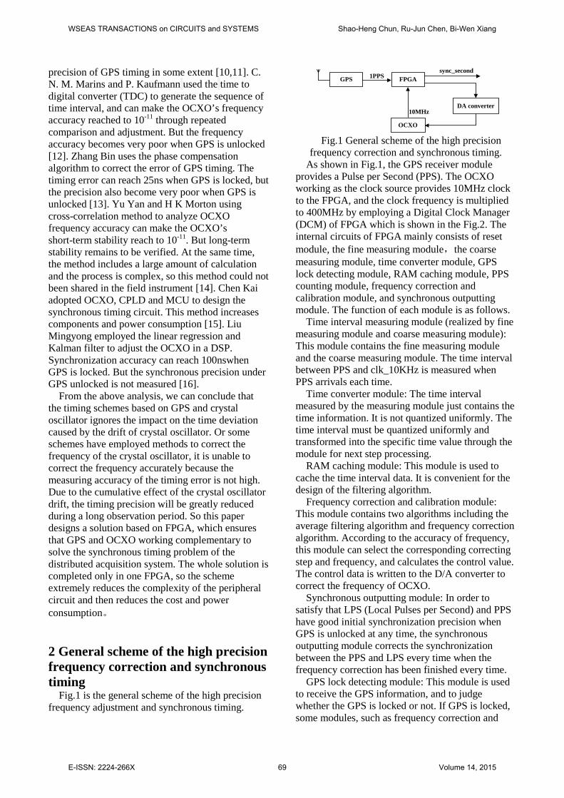
Fig.1 is the general scheme of the high precision frequency adjustment and synchronous timing.
GPS FPGA
OCXO
DA converter
sync_second1PPS
10MHz
Fig.1 General scheme of the high precision
frequency correction and synchronous timing. As shown in Fig.1, the GPS receiver module
provides a Pulse per Second (PPS). The OCXO working as the clock source provides 10MHz clock to the FPGA, and the clock frequency is multiplied to 400MHz by employing a Digital Clock Manager (DCM) of FPGA which is shown in the Fig.2. The internal circuits of FPGA mainly consists of reset module, the fine measuring module,the coarse measuring module, time converter module, GPS lock detecting module, RAM caching module, PPS counting module, frequency correction and calibration module, and synchronous outputting module. The function of each module is as follows.
Time interval measuring module (realized by fine measuring module and coarse measuring module): This module contains the fine measuring module and the coarse measuring module. The time interval between PPS and clk_10KHz is measured when PPS arrivals each time.
Time converter module: The time interval measured by the measuring module just contains the time information. It is not quantized uniformly. The time interval must be quantized uniformly and transformed into the specific time value through the module for next step processing.
RAM caching module: This module is used to cache the time interval data. It is convenient for the design of the filtering algorithm.
Frequency correction and calibration module: This module contains two algorithms including the average filtering algorithm and frequency correction algorithm. According to the accuracy of frequency, this module can select the corresponding correcting step and frequency, and calculates the control value. The control data is written to the D/A converter to correct the frequency of OCXO.
Synchronous outputting module: In order to satisfy that LPS (Local Pulses per Second) and PPS have good initial synchronization precision when GPS is unlocked at any time, the synchronous outputting module corrects the synchronization between the PPS and LPS every time when the frequency correction has been finished every time.
GPS lock detecting module: This module is used to receive the GPS information, and to judge whether the GPS is locked or not. If GPS is locked, some modules, such as frequency correction and
WSEAS TRANSACTIONS on CIRCUITS and SYSTEMS Shao-Heng Chun, Ru-Jun Chen, Bi-Wen Xiang
E-ISSN: 2224-266X 69 Volume 14, 2015
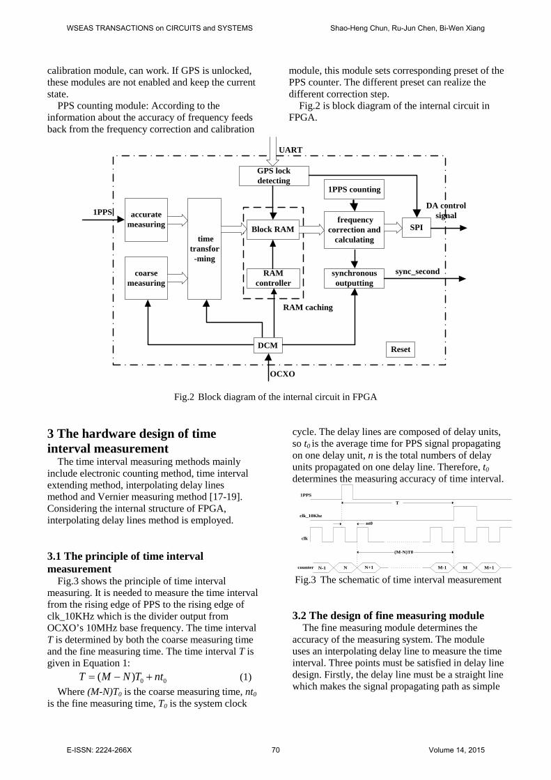
calibration module, can work. If GPS is unlocked, these modules are not enabled and keep the current state.
PPS counting module: According to the information about the accuracy of frequency feeds back from the frequency correction and calibration
module, this module sets corresponding preset of the PPS counter. The different preset can realize the different correction step.
Fig.2 is block diagram of the internal circuit in FPGA.
coarse measuring
accurate measuring
time transfor-ming
Block RAM
DCM
RAM controller
frequency correction and
calculating
synchronous outputting
1PPS
sync_second
DA control signal
OCXO
RAM caching
1PPS counting
Reset
SPI
GPS lock detecting
UART
Fig.2 Block diagram of the internal circuit in FPGA
3 The hardware design of time interval measurement
The time interval measuring methods mainly include electronic counting method, time interval extending method, interpolating delay lines method and Vernier measuring method [17-19]. Considering the internal structure of FPGA, interpolating delay lines method is employed.
3.1 The principle of time interval measurement
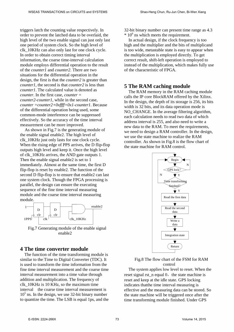
Fig.3 shows the principle of time interval measuring. It is needed to measure the time interval from the rising edge of PPS to the rising edge of clk_10KHz which is the divider output from OCXO’s 10MHz base frequency. The time interval T is determined by both the coarse measuring time and the fine measuring time. The time interval T is given in Equation 1:
0 0( )T M N T nt= − + (1) Where (M-N)T0 is the coarse measuring time, nt0
is the fine measuring time, T0 is the system clock
cycle. The delay lines are composed of delay units, so t0 is the average time for PPS signal propagating on one delay unit, n is the total numbers of delay units propagated on one delay line. Therefore, t0 determines the measuring accuracy of time interval.
1PPS
clk_10Khz
clk
counter N-1 N N+1 M-1 M M+1
nt0
(M-N)T0
T
Fig.3 The schematic of time interval measurement 3.2 The design of fine measuring module
The fine measuring module determines the accuracy of the measuring system. The module uses an interpolating delay line to measure the time interval. Three points must be satisfied in delay line design. Firstly, the delay line must be a straight line which makes the signal propagating path as simple
WSEAS TRANSACTIONS on CIRCUITS and SYSTEMS Shao-Heng Chun, Ru-Jun Chen, Bi-Wen Xiang
E-ISSN: 2224-266X 70 Volume 14, 2015

as possible. Secondly, the propagating time of the delay unit must be determined, which enables the statistics and calculation of delay time. Thirdly, the overall delay time of a delay line must be larger than the period of system clock, in another words, the delay line must be long enough. Based above three points, XC6SLX9 from Xilinx is chosen as FPGA in the design [20].
There exist a lot of methods to build delay line in FPGA. Generally, counter, adder and multiplier are used commonly. Among all the methods, using special carry line units to build the delay line owns the best resolution. In this design, the chip we select contains abundant special carry line unit (CARRY4), and it is easy to use.
Fig.4 is the structure of carry line unit (CARRY4). CARRY4 mainly consists of multiplexers (MUXCY) and special XOR gates(XORCY) [21].
MUXCY
MUXCY
MUXCY
MUXCY
CARRY4
CO(3:0)
O(3:0)
D(3:0)
S(3:0)
CYINIT
S(3)
S(2)
S(1)
S(0)
CO(3)
CO(2)
CO(1)
CO(0)
O(0)
O(1)
O(2)
O(3)
XORCY
XORCY
XORCY
XORCY
D(3)
D(2)
D(1)
D(0)
Slice Carry Logic
CI
0 1
0
0
0
1
1
1
Fig.4 The structure of carry line unit(CARRY 4) In order to code the measuring time interval, the
input setting of CARRY4 can be configured as shown in Tab.1.
Tab.1 The input configuration of CARRY4 Pin Configuration value
CYINIT 0 CI Carry signal
S(3:0) “1111” D(3:0) “xxxx”
The carry signal is connected to the port CI and then propagates along the delay line. S(3:0) is used to configure the signal propagating path. When S(3:0) is equal to "1111", it indicates that the signal propagates along the path of MUXCY port 1. D(3:0) is used to configure corresponding values for MUXCY port 0. According to Fig.4, when S(3:0) is equal to “1111”, the output signal O(3:0) is only determined by S(3:0) and the carry signal. So the value of D(3:0) is not considered and it is denoted as “xxxx”. Before the carry signal arrives, all of the output signal O is 1. When carry signal propagates from low bit to high bit of the delay line, CO switches to 1 from 0 one by one. O(3:0) is complementary to the signal CO and so switches to 0 from 1one by one. Then we can get the output of O as "111... 111000... 000" where the MSB is 1and the LSB is 0. This output can be coded conveniently.
The number of zero in the output indicates the number of delay units the carry signal having propagated before the rising edge of the system clock next to the carry signal. The number of ones is the number of delay units the carry signal which does not reach. Therefore, once the number of zero is known, the total number of delay units that the carry signal have propagated will be determined. Then the result of fine time interval can be calculated based on the number of zero.
To calculate the value of the fine time interval, it is necessary to measure the delay of each delay unit. Modesim6.5SE is employed to simulate the circuit which have finished post-route in FPGA. Through the post-route simulation, the delay of each delay unit can be simulated with high precision. In this design, the time node of output signal changing from 1 to 0 can be simulated. The simulated result is shown in Tab.2.
Tab.2 The simulated result of delay lines PPS input time (ps) 300000 300033 300043 300115 300125 300197
Number of 0 102 100 98 96 94 92 PPS input time(ps) 300207 300278 300288 300359 300369 300439
Number of 0 90 88 86 84 82 80 From table.2, we can find two zero changing
together, and the delay time of delay line is 71ps and 10ps. Therefore, as long as the number of zero is counted, the propagated time of the PPS signal
WSEAS TRANSACTIONS on CIRCUITS and SYSTEMS Shao-Heng Chun, Ru-Jun Chen, Bi-Wen Xiang
E-ISSN: 2224-266X 71 Volume 14, 2015

along the delay line can be calculated with high resolution.
There is a slice unit in each CLB of Xc6slx9, and there is a CARRY4 in each slice. There are 60 slices totally in the longitudinal direction, so a 240-bit delay line can be built in the FPFA. In the design, we choose 320MHz as the system clock, so
the clock cycle is 3.125ns. According to the inequality (71 + 10) * (240/4) = 4860ps > 3.125 ns, building a 240-bit delay line to measure the fine time interval is enough.
As shown in Fig.5 is the schematic of the fine time interval measurement.
The first
column triggers
8bits priority encoder
D
The second column triggers
carry_in
Delay line
1PPS enable1clkclk
1
clr Q0
Fig.5 The schematic of the fine time interval measurement circuit
Fig.5 shows that PPS is the clock of the D flip-flop and the D flip-flop outputs the carry signal CI. When carry signal transmits along the delay line, the measurement data of fine time interval is generated. The data is latched when the rising edge of system clock reaches. Q0 is the output of the trigger’s lowest bit, and is divided into two signals. The two signals are inverted through NOT gate and one connects to the clear signal of D flip-flop, the other one is an enable signal which is the input of the coarse time interval measurement module. The second column trigger is used to reduce metastable condition, which ensures the data have entered stable state before the data is encoded. The delay line is made up of 240 delay units. In order to encode the output of the delay line, 8-bit priority encoder is employed and the lowest bit is assigned with the highest priority. 3.3 The design of the coarse time interval measuring module
The coarse time interval measuring module is used to measure the value of (M-N)T0 shown in the formula (1).This module mainly employs counters to complete the measuring. In the design, the frequency of system clock clk is 320MHz. So if we divide the system clock to 1Hz and measure the interval time between the 1Hz signal and the PPS, a 29-bit counter must be used. This not only wastes the hardware resource but also expands the bits of the data to increase the probability of metastable state. In order to solve above problems, we use a 10KHz signal based on the system clock by 3200 division to replace the second pulse. Then a 16-bit counter can meet the requirement of the coarse time interval measuring.
But it is need to note that the PPS has random jitter as dozens of nanoseconds. The executing sequence of both the coarse time interval measuring module and the fine time interval measuring module may be disordered. In order to prevent this case occurring, the module starts to count when the rising edge of PPS have been detected. The counter is used to delay a given time to make the rising edge of the PPS locate at the middle area of a clk_10KHz period and then the system clock is been divided by 3200 to generate the signal clk_10KHz.
Consider the factor that the frequency of clk and clk_10KHz is 320MHz and 10MHz respectively, the 16-bit counter is selected. As shown in Fig.6 is the schematic of the coarse time interval measuring module.
16bits counter
coarse measuring integration
ce
ce
clk
clk
enable1
enable2
counter1
counter2
Fig.6 The schematic of the coarse time interval
measuring circuit From Fig.6, the enable signal enable1 is
generated by the fine time interval measuring module, the enable signal enable2 is generated by the circuit shown in Fig.7. The Fig.6 shows that the 16-bit counter is always work using the system clock clk. When the enable signal enable1 and enable2 are in high level, the corresponding
WSEAS TRANSACTIONS on CIRCUITS and SYSTEMS Shao-Heng Chun, Ru-Jun Chen, Bi-Wen Xiang
E-ISSN: 2224-266X 72 Volume 14, 2015
triggers latch the counting value respectively. In order to prevent the latched data to be overlaid, the high level of the two enable signal can just only last one period of system clock. So the high level of clk_10KHz can also only last for one clock cycle. In order to obtain correct timing interval information, the coarse time-interval calculation module employs differential operation to the result of the counter1 and counter2. There are two situations for the differential operation in the design, the first is that the counter2 is greater than counter1, the second is that counter2 is less than counter1. The calculated value is denoted as counter. In the first case, counter = counter2-counter1, while in the second case, counter =counter2+0xffff+0x1-counter1. Because of the differential operation being used, some common-mode interference can be suppressed effectively. So the accuracy of the time interval measurement can be more improved.
As shown in Fig.7 is the generating module of the enable signal enable2. The high level of clk_10KHz just only lasts for one clock cycle. When the rising edge of PPS arrives, the D flip-flop outputs high level and keep it. Once the high level of clk_10KHz arrives, the AND gate outputs 1. Then the enable signal enable2 is set to 1 immediately. Almost at the same time, the first D flip-flop is reset by enable2. The function of the second D flip-flop is to ensure that enable2 can last one system clock. Though the FPGA processing is parallel, the design can ensure the executing sequence of the fine time interval measuring module and the coarse time interval measuring module.
clr1PPS
clrclk clk_10KHz
D Denable21
Fig.7 Generating module of the enable signal
enable2
4 The time converter module The function of the time transforming module is
similar to the Time to Digital Converter (TDC). It is used to transform the time information from the fine time interval measurement and the coarse time interval measurement into a time value through addition and multiplication. The frequency of clk_10KHz is 10 KHz, so the maximum time interval the coarse time interval measurement is 105 ns. In the design, we use 32-bit binary number to quantize the time. The LSB is equal 1ps, and the
32-bit binary number can present time range as 4.3 * 106 ns which meets the requirement.
In actual design, if the clock frequency is too high and the multiplier and the bits of multiplicand is too wide, metastable state is easy to appear when the multiplication is employed directly. To get correct result, shift-left operation is employed to instead of the multiplication, which makes fully use of the characteristic of FPGA. 5 The RAM caching module
The RAM memory in the RAM caching module calls the IP core BlockRAM offered by the Xilinx. In the design, the depth of its storage is 256, its bits width is 32 bits, and its data operation mode is NO_CHANGE. In the average filtering algorithm, each calculation needs to read two data of which address interval is 255, and also need to write a new data to the RAM. To meet the requirements, we need to design a RAM controller. In the design, we use the state machine to realize the RAM controller. As shown in Fig.8 is the flow chart of the state machine for RAM control.
Begin
GPS lock?
Read the first data
Read the second data
Write a data
Integration state
Return
Y
N
Y
N
Time transforming finished?
Fig.8 The flow chart of the FSM for RAM
control The system applies low level to reset. When the
reset signal rst_n equal 0,the state machine is reset and keep at the idle state. GPS locking indicates thatthe time interval measuring is effective and the measuring data can be stored. So the state machine will be triggered once after the time transforming module finished. Under GPS
WSEAS TRANSACTIONS on CIRCUITS and SYSTEMS Shao-Heng Chun, Ru-Jun Chen, Bi-Wen Xiang
E-ISSN: 2224-266X 73 Volume 14, 2015

locked situation, the time interval is measured once per second and the measured value is stored into the RAM. If GPS is unlocked, the measuring data will be abandoned. In the design, U-BLOX LEA-6T is chosen as the GPS oem board. UART port is used for communicating between the GPS module and FPGA. The GPS lock detecting module is used to detect the receiving data from UART port. When GPS locks, the flag signal is set to 1. Once GPS unlocks, the flag signal is set to 0.
When the state machine starts working, it will enter into the reading state firstly through set the RAM enabling signal ena and reset the writing enabling signal wea. In reading state, the initial address need to be saved and then the address will be assigned to the RAM to read the corresponding data. The way reading the second data is similar to the first data but for the address. The address is the initial address plus 255. In order to read data by the frequency correction and calibration module correctly, a flag signal is set after reading a data and the high level of the flag signal can just only last one system clock. For the reading operation, if the two data addresses read in first time are 0 and 255 respectively, then the data addresses read in second time are 1 and 0 and the data addresses read in third time are 2 and 1. Then the rule is followed. After the reading state, the machine enters into the writing state. The initial address previously saved is assigned to the writing address. And then the machine will enter into the integration state. In this state, the initial address adds 1 and the new address is regard as the initial address for the next operation. And the clock state of the RAM is reset to 0, both the ena and wea are reset to 0. Then the machine finally returns to the idle state and waits for the next operation. 6 The frequency correction 6.1 The principle of the frequency correction
Whenever GPS is unlocked, the system can automatically switch to the locale pulse per second (LPS) to replace the PPS for right work. So it requires that LPS and PPS keep high synchronous precision all the time. To meet the requirement, the system needs to satisfy two points. The first one is the frequency of OXCO needs to be corrected accurately, the second is LPS and PPS has a high initial synchronization precision. The frequency correction can decrease the deviation between the actual measuring frequency and standard frequency to a certain range. In another word, we can gain
higher frequency accuracy of OCXO through the frequency correction. Eq.2 is the calculating method of the frequency accuracy.
1 0
0
f fAf−
= (2)
Where f1 is the actual frequency, f0 is the standard frequency.
There are three methods for frequency accuracy measuring, the measuring frequency method, the measuring period method and the measuring phase method. Among the three methods, the measuring period method is the most widely used and most easily to implement. And so the measuring period method is employed in the design. As shown in Fig.9 is the schematic of the measuring period method.
PPS
clk_10KHz
T1 T2
T
Fig.9 The schematic of the measuring period method
T1 and T2 indicate respectively the two interval time between the measured signal and the standard signal. As a result, the frequency accuracy can be written as the following format.
2 1T TAT−
= (3)
6.2 The design of the filtering algorithm There are two main noises affect the frequency
accuracy. One is the frequency drift of OCXO and it is denoted as Q0. The other one is the noise brought by PPS and it is denoted as Q1.Then the measuring value of the time interval can be expressed by Eq.4.
0 1X Q Q= + (4) The average filtering algorithm is employed to
suppress the noise. Eq.5 is the formula of the average filtering algorithm.
1
0
1( ) ( )M
jY i X i j
M
−
=
= +∑ (5)
Where M is the moving window, X(j) is the measuring time interval, Y(i) is the average value for M points. Because the PPS’s period is 1s, T is equal to 1012 ps. Considering Eq.3 and Eq.5, the frequency accuracy A can be written as Eq.6.
WSEAS TRANSACTIONS on CIRCUITS and SYSTEMS Shao-Heng Chun, Ru-Jun Chen, Bi-Wen Xiang
E-ISSN: 2224-266X 74 Volume 14, 2015
M -1 M -1
12j=0 j=0
Y(n)-Y(n -1) 1 1 1 1A= = ( X(n+ j)- X(n -1+ j) )= (X(n -1+ M)- X(n -1))T T M M M * 10∑ ∑ (6)
Considering Eq.4 and Eq.6, the frequency accuracy A can be written as Eq.7.
0 0 1 112 12
1 1( ( 1 ) ( 1)) ( ( 1 ) ( 1))*10 *10
A Q n M Q n Q n M Q nM M
= − + − − + − + − − (7)
As known from Eq.7, the two kinds of noise are reduced to 1/M relatively to the original noise through the average filtering algorithm. The practical verification shows that the filtering algorithm can suppress the noise effectively.
7 The frequency correction method and synchronous outputting module 7.1 The frequency correction method to the OCXO
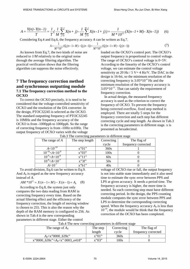
To correct the OCXO precisely, it is need to be considered that the voltage-controlled sensitivity of OCXO and the resolution of the DA converter. In the design, PTOC32245 is selected as the OCXO. The standard outputting frequency of PTOC32245 is 10MHz and the frequency accuracy of the OCXO is from -1000ppb to 1000ppb. So the range of correcting frequency is from -10Hz to10Hz. The output frequency of OCXO varies with the voltage
loaded on the OCXO’s control port. The OCXO’s output frequency is proportional to control voltage. The range of OCXO’s control voltage is 0~5V. According to the linearity of the OCXO’s control voltage, we can estimate the control voltage sensitivity as 20 Hz / 5 V= 4 Hz/V. The DAC in the design is 16-bit, so the minimum resolution of the correcting frequency is 3.05*10-4 Hz and the minimum resolution of the frequency accuracy is 3.05*10-11. That can satisfy the requirement of frequency correction.
In actual design, the measured frequency accuracy is used as the criterion to correct the frequency of OCXO. To prevent the frequency being corrected overflow, fixed step method is employed. There are totally 5 steps for the frequency correction and each step has different correcting cycle and step length. As shown in Tab.3 is the correcting parameters in different stage. x is presented as hexadecimal.
Tab.3 The correcting parameters in different stage The range of A The step length Correcting
cycle The flag of
frequency corrected A<10-10 x”01” 360s 1
10-10<A<10-9 x”03” 100s 0 10-9<A<10-8 x”11” 60s 0 10-8<A<10-7 x”3f” 50s 0
A>10-7 x”b1” 40s 0 To avoid division, Eq.6 can be written to Eq.9.
And A0 is regard as the new frequency accuracy instead of A.
120*10 ( 1 ) ( 1)AM X n M X n A= − + − − = (8)
According to Eq.8, the system just only compares the two data reading from RAM in correcting frequency every time. Based on the actual filtering effect and the efficiency of the frequency correction, the length of moving window is chosen to 255. This is also the reason why the depth of the RAM memory is configured to 256. As shown in Tab.4 is the new corresponding parameters in different stage. Either the control
voltage of OCXO rise or fall, the output frequency is not into stable state immediately and it also need time to estimate the sync error between PPS and LPS at given accuracy. It needs a period time. The frequency accuracy is higher, the more time is needed. So each correcting step must have different correcting period. In the design, the PPS counting module computes the sync error between PPS and LPS to determine the corresponding correcting speed. When the frequency accuracy A0 is less than 10-10, the module would be think that the frequency correction of the OCXO has been completed.
Tab.4 The new correcting parameters in different stage The range of A0 The step
length Correcting
cycle The flag of
frequency corrected A0<x”0000_639c” x”01” 360s 1
x”0000_639c”<A0<x” 0003_e418” x”03” 100s 0
WSEAS TRANSACTIONS on CIRCUITS and SYSTEMS Shao-Heng Chun, Ru-Jun Chen, Bi-Wen Xiang
E-ISSN: 2224-266X 75 Volume 14, 2015

x”0003_e418”<A0<x”0026_e8f0” x”11” 60s 0 x”0026_e8f0”<A0<x”0185_1960” x”3f” 50s 0
A0>x”0185_1960” x”b1” 30s 0 When the system is powered on, every module is
reset. After the reset, the system writes a 16-bit data data_ctr to DA converter through the SPI bus. The DA converter converts the data to the corresponding analog voltage and output the voltage to the OCXO’s control port. During the frequency correction, the frequency correction and calibration module reads the two data x (n) and x (n-1+M) from the RAM firstly. Then the two data would be compared. After that the frequency accuracy A0 can be calculated directly. If x (n) is greater than x (n-1+M), the current frequency of OCXO is higher. Then the module chooses the corresponding correction step and frequency based on the value of A0. The data data_ctr will minus the step and is written to the DA converter through the SPI bus. The correction frequency is controlled by the PPS counting module. After the frequency correction and calibration module calculates the frequency accuracy A0 of the OCXO, it will feedback correcting cycle to PPS counting module. When the correcting cycle has been elapsed, the module can generate a signal to trigger the frequency correction and calibration module. After the module is triggered, the two data x(n) and x(n-1+M) will be read and the frequency accuracy A0 can be recalculate again. Based on the value of A0, the correction step and frequency would be chosen again and all processes would be repeated. According to the design of the algorithm, the OCXO’s frequency will be continued to be corrected until the A0 is less than 10-10. When A0 is less than 10-10, the system will keep the current state 6 minutes. After 6 minutes, A0 will be recalculated and the frequency can be corrected again.
It needs to note that when the GPS is locked, the two data stored in RAM are output per second under the RAM controller. But the frequency correction and calibration module does not read the two data, only reads the two data when the module is triggered by PPS counting module. If x (n) is less than x (n-1+M), the current frequency of OCXO is lower. Then all steps about the frequency correction are similar to the above solution except that the data data_ctr plus the step instead of minus.
About the initial value of the data data_ctr, it is set less than half of x"FFFF" slightly. When the system is powered on, all of the RAM data are 0 and is written by a data per second. So it needs about 256s to be written full. During the period of
256s, the first reading data always is 0. Then the system automatically judges that the frequency accuracy A0 is more than 10-7 and the step is x”b1”, so the data data_ctr written to ADC will always add the corresponding step. Because OCXO is the most stable when the control voltage is near the middle voltage, the initial value of data_ctr is chosen as a data less than half of 0x "FFFF" slightly. The data data_ctr adds the step 0x”b1” every 30s, so data_ctr will add x”b1” eight times. In the actual design, by combining with actual situation, the initial value of data_ctr is set to x”7eff”.
Based on long-term test, it needs about 45 minutes from the system powering on to finishing the frequency correction, which includes the 15min heating time of the OCXO. Once the frequency correction is finished, the frequency is corrected again after unlock spending about 200s. The Tab.5 shows the time needed by frequency correction again after the GPS unlocking different duration.
Tab.5 The time of frequency locking again The time of GPS unlock The time of correcting
frequency again 1h 15min 2h 16min 4h 14min 8h 15min
12h 16min 16h 18min 20h 16min 24h 17min
As shown in Tab.5, once the frequency correction has finished, the time of correcting frequency again is almost equal when GPS locks, no matter the GPS unlocks 1h or 24h This indicates that when GPS is unlock, the data previously stored in the Block RAM is still valid. And it also confirms that the noise brought by PPS signal is random noise and the noise will not accumulate with long-running. 7.2 Synchronous outputting module
In order to satisfy the requirement that LPS and PPS has a high synchronous precision all the time, it is employed that a scheme which can correct the synchronization error every time when the frequency correction finishes. As shown in Fig.10 is the block diagram of the synchronous outputting module.
WSEAS TRANSACTIONS on CIRCUITS and SYSTEMS Shao-Heng Chun, Ru-Jun Chen, Bi-Wen Xiang
E-ISSN: 2224-266X 76 Volume 14, 2015

1bit counter
D
DQ
clr
en en
clkPPS
1LPS1
D
DQ
clr
en en
clkPPS
1
Frequency dividing
LPS2
clr
clr
PPS
LPS3
enable1
enable2
freq_lock
enable1 gps_lock
sync_second
gps_lock
Frequency dividing
MUX
MUX
Fig.10 The diagram of Synchronous outputting module
The signal freq_lock is generated by the frequency correction and calibration module. When A0 is less than 10-10, it indicates that the frequency correction has been completed. Then the signal freq_lock is set and the high level of freq_lock just lasts a period of system clock. The 1-bit counter is triggered by the high level of freq_lock. The counter is not work immediately, but wait for 5min before starting count. The 5min is the time that the OCXO’s output frequency becomes stable. When it is powered on, the system is reset and the signal enable1 and enable2 are reset. The counter employs a 1-bit variable to count. When the variable equals to 1, enable1 is set to 1. The signal enable2 is generated by invert the signal enable1, so enable2 is set to 0. When the variable is equal to 0, enable1 is set to 0 and enable2 is set to 1. And the system will repeat above procedure again and again.
When enable1 is 0, the first line, which consists of a D flip-flop and a frequency dividing module, is reset, and the second line is enabled. On the contrary, when enable1 is 1, the first line is enabled and the second is reset. In the first line, the D flip-flop is enabled under enable1 equal to 1. After the rising edge of PPS reaching, the D flip-flop output high level to enable the frequency dividing module. The module begins to dividing the system clock to generate LPS when the rising edge of the system clock next PPS is reaching. This scheme can ensure the synchronous precision reach 2.5ns at least in the beginning time between PPS and LPS. LPS is set to 1 firstly and the high level last 0.1s which is similar to PPS.
The function of the second channel is same to the first one. Which channel’s signal is selected as output is determined by the first multiplexer. When enable1 is 1, the first channel signal LPS1 is output. When enable1 is 0, the second channel signal LPS2is output. The second multiplexer’s output is determined by the GPS locking signal. When the locking signal is 1, PPS is the output. And when the signal is 0, LPS3 is the output.
Whenever the frequency correction has been completed, the module corrects the synchronization between the LPS and PPS, which ensures that the LPS can replace of PPS to work when GPS is unlocked in any of time. 8 The effect of PPS and OCXO sync
As shown in Fig.11 is the debugging diagram of the prototype. From Fig.11, we can find that the peripheral circuit is very simple
Oscilloscope
GPS FPGA
OCXO
Fig.11 The debugging diagram of prototype for GPS and OCXO timing
As shown in Fig.12 is the diagram of internal data which is grabbed by ChipScope, which is an online debugging tool after the frequency correction finishes.
Fig.12 The diagram of internal data when frequency corrected
In Fig.12, data_temp is a 32-bit value of time interval and data_in_temp1 is another value which’s address difference is 255 from data_temp.
Data_in_temp2 is the differential value of both above. The differential value is x"0000_49b7" less than x"0000 _639c", so it indicates that the
WSEAS TRANSACTIONS on CIRCUITS and SYSTEMS Shao-Heng Chun, Ru-Jun Chen, Bi-Wen Xiang
E-ISSN: 2224-266X 77 Volume 14, 2015

frequency accuracy achieve the required range and the frequency correction has completed.
The sampling rate of distributed acquisition systems of Induced Polarization method (IP), Magnetotelluric method (MT) and Audio Magnetotelluric method(AMT) are 64Hz, 2.4KHz, 24KHz respectively, which is researched by a
Central South University in China. The synchronous precision is commonly 100 times to sampling rate. So the synchronous precision of IP, MT and AMT are respectively 156.25 us, 4166 ns and 416 ns. As shown in Fig.13 are the different synchronous precision in every three hours under GPS locking.
PPS
LPS
PPS
LPS
(1) (2)
PPS
LPS
PPS
LPS
(3) (4)
Fig.13 The synchronous comparison at different times (GPS lock) From these figures, the synchronous precision
between the local second pulse and PPS is always remained at about 50ns. Considering the dozens of nanoseconds random jitter of the PPS, the synchronous precision designed in the paper can achieve 30ns under GPS locking, or even higher. The longer the running time is, the better the synchronous precision will be gained. So whether adopt the local second pulse or PPS to give timing synchronously to the distributed acquisition system, the synchronous precision of them can meet the timing requirement of all distributed acquisition systems for electrical prospecting.
Fig.14 shows the different synchronous precisions for the GPS unlocked in different time after frequency correction finished once.Fig.14.1 is the synchronous precision diagram when the GPS antenna disconnected in the beginning. Fig.14.2 is
the synchronous precision diagram in the case of the OCXO has drifted 410ns.
PPS
LPS
(1)
WSEAS TRANSACTIONS on CIRCUITS and SYSTEMS Shao-Heng Chun, Ru-Jun Chen, Bi-Wen Xiang
E-ISSN: 2224-266X 78 Volume 14, 2015

tunnel or underground environment where GPS entirely unlock.
The Fig.16 shows the time interval and the gradient of the interval time in different time and in different temperature.
0 5 10 15 20-10
0
10
20
30
40
Tim
e in
terv
al v
alue
(us)
0 1 2 3 4 5 6 7 8 9 10 11 12 13 14 15 16 17 18 19 20 21 22 23 2410
11
12
13
14
15
16
17
18
19
20
21
22
23
24
25
Time(h)
Tem
pera
ture
( °)
Temperature
Time interval value
(1)
0 1 2 3 4 5 6 7 8 9 10 11 12 13 14 15 16 17 18 19 20 21 22 23 24-5
-4
-3
-2
-1
0
1
2
3
4
5
6
7
8
9
10
Gra
dien
t(us)
0 5 10 15 2010
11
12
13
14
15
16
17
18
19
20
21
22
23
24
Tem
pera
ture
( °)
Time(h)
temperature
gradient
(2)
Fig.16 The accuracy of synchronization and the gradient Fig.16.1 and Fig.16.2 are respectively the time
interval and the gradient of the time interval in different time and in different temperature. As known from the two figures, the OCXO frequency accuracy is high when the GPS antenna is disconnected in the beginning. There is not accumulative error in this time and LPS can replace PPS to work well. When the OCXO has worked 12h, the changes of the accumulative error and
temperature have obvious impact on the frequency accuracy. 9 Conclusion
This paper has researched that how to correct frequency accuracy and improve the synchronous precision in the OCXO and GPS timing. All the program of synchronous timing is completed in a
WSEAS TRANSACTIONS on CIRCUITS and SYSTEMS Shao-Heng Chun, Ru-Jun Chen, Bi-Wen Xiang
E-ISSN: 2224-266X 79 Volume 14, 2015

FPGA. Based on the long-term test, the solution can well combine the advantages of GPS timing and OCXO timing, and so to overcome the disadvantages of GPS timing.
This scheme can correct the frequency accuracy of OCXO to reach 10-10, and the accuracy is about dozens of picoseconds. So the frequency accuracy is high. In order to ensure the synchronous precision in any time, when the frequency correction is finished in every time, the synchronous outputting module corrects the synchronization between the PPS and LPS. The moving average filtering algorithm employed in the design can suppress random noise brought by PPS effectively. After frequency correction is completed, the synchronous precision can even reach 410ns, 1.6us, 2us and 33us respectively for the GPS unlock up to 150min, 6h, 12h, and 24h.The solution is not only meets the synchronous timing requirements of all the distributed acquisition systems for electrical prospecting, but also can be applied in the other industry field which also have high requirement for synchronous precision. The high synchronous precision can still be kept after the system working for a long time. At the same time, all modules are designed in one FPGA which simplifies the peripheral circuit furthest, so this scheme reduces the cost and power obviously. The performance of the system is controlled by the current level of hardware, so upgrading the system only need to replace the corresponding hardware in the future, which greatly shortens the development cycle. Reference [1]He Ji-shan, Development and prospect of
electrical prospecting method, Chinese Journal of geophysics, Vol.40, 1997, pp.308-316.
[2]Ye yixin, Deng Juzhi, Li man, etal, Application status and vistas of electromagnetic methods
to deep ore prospecting, Progress in geophysics, Vol.26, No.1, 2011,pp.327-334. [3]Zhang Shulian, Wang Hui, Zhang Zhiqiang, etal,
Analysis of international proprietary technology development of geophysical instrument, Progress in geophysics, Vol.26, No.3, 2011, pp.1120-1130.
[4]Zhao Guoze, Chen Xiao bin, Tang Ji, Advanced geo-electromagnetic methods in China, Process in Geophsics, Vol.22, No.4, 2007, pp.1171-1180.
[5]Di QingYun, Fang GuangYou, Zhang YiMin, Research of the Surface Electromagnetic Prospecting(SEP)system, Chinese journal
Geophys (in Chinese), Vol.56, No.11, 2013,pp. 3629-3639.
[6]W. Lewandowski, J. Azoubib, W. J. Klepczynski, GPS: Primary tool for time transfer.IEEE, Vol. 87, No. 1, 1999, pp. 163-172.
[7]A.Moreno-Muñoz, V. Pallarés-López, I. M. Moreno-García,etal, Embedding Synchronized Measurement Technology for Smart Grid Development. IEEE transactions on Industrial informatics,Vol.9, No.1, 2013, pp.52-61.
[8] Huang Xiang, Jiang Daozhuo, A high accuracy time keeping scheme based on GPS, Automation of Electric Power Systems(in Chinese), Vol.34, No.18, 2010, pp. 74-77.
[9] Zeng Xiangjun, Yin Xianggen, Li K K, et al, Methods for monitoring and correcting GPS-clock, Proceedings of the Chinese society for electrical engineering,2002,22(12):41-46..
[10]Agarwal V, Arya H, Bhaktavatsala S, Design and development of a real-time DSP and FPGA-based integrated GPS-INS system for compact and low power applications, IEEE Transactions on Aerospace and Electronic Systems, Vol.45, No.2, 2009, pp.443-454.
[11]Graham W P, Analysis of a nonlinear least squares procedure used in global positioning systems, IEEE Transactions on Signal Processing, Vol.58, No.9, 2010, pp.5426-4534.
[12]C. N. M. Marins, P. Kaufmann, A. A. Ferreira, Jr, etal, Precision Clock and Time Transfer on a Wireless Telecommunication Link, IEEE Transactions on Instrumentation and measurement, Vol.59, No.3, 2010, pp.512-518.
[13]Zhang Bin, Zhang Donglai, GPS-based Precision Clock Online Frequency Calibration and Time Service, Proceedings of the Chinese Society for Electrical Engineering, Vol.32, No.10, 2012, pp.160-167.
[14]Yanhong kou, Yu morton. 2013.Oscillator Frequency Offset Impact on Software GPS Receivers and Correction Algorithms. IEEE transactions on Aerospace and Electronic System, Vol.49, NO.4 OCTOBER, 2013, pp.2158-2178.
[15]Chen Kail, Jing JianEn, Wei WenBo, etal, Numerical simulation and electrical field recorder development of the marine electromagnetic method using a horizontal towed-dipole source, Chinese journal of geophysics, Vol.56, No.11, 2013, pp.3718-3727.
[16]Liu Mingyong, Zhang bingyu, Zhang lichuan, Design and implementation of Clock Synchronization Control Algorithm for
WSEAS TRANSACTIONS on CIRCUITS and SYSTEMS Shao-Heng Chun, Ru-Jun Chen, Bi-Wen Xiang
E-ISSN: 2224-266X 80 Volume 14, 2015

Multi-AUV Collaboration Missions, Journal of Northwestern Polytechnical University, Vol.31, No.6, 2013, pp.848-852.
[17] Wen Xuan, Deng Jia-hao, Li Yue-qin, Data-processing of high accuracy pulse laser range measurement. Infrared and laser engineering, Vol.36, No.2, 2007, pp.150-153.
[18]Sun Jie,Pan Jifei, Methods of High Precision Time-Interval Measurement[J].Computer Measurement & Control,VOL.15, No.02, 2007, pp.145-148.
[19]Zhang Yan, Huang Peicheng, High-Precision Time Interval measurement techniques and Methods, Progress in astronomy, Vol.24, No.01, 2006, pp.10-15.
[20] Spartan-6 Family Overview, Xilinx, http://china.xilinx.com/support/documentation/data_sheets/ds160.pdf
[21]Spartan-6 FPGA Configurable Logic Block, Xilinx, http://china.xilinx.com/support/documentation/user_guides/ug384.pdf
WSEAS TRANSACTIONS on CIRCUITS and SYSTEMS Shao-Heng Chun, Ru-Jun Chen, Bi-Wen Xiang
E-ISSN: 2224-266X 81 Volume 14, 2015