fraunhofer institute for solar energy systems, ise pv ... · fraunhofer institute for solar energy...
TRANSCRIPT

Fraunhofer Institute for Solar Energy Systems, ISE
PV STUDY INDIA Assessing the Cost of Production for 100MWp and 1GWp PV Value Chain

Fraunhofer ISE
PV STUDY INDIA Assessing the Cost of Production for 100MWp and 1GWp PV Value Chain
B. Goraya, L. Friedrich, J. Rentsch 8/30/2016

1
Table of Contents 1. Executive Summary ......................................................................................................................... 2
2. Introduction ..................................................................................................................................... 4
3. The PV Value chain and minimum size requirements ..................................................................... 6
3.1 Vertical Integration .................................................................................................................. 6
3.2 Status of chosen technology ................................................................................................... 7
3.3 Minimum size requirements and definition of cases .............................................................. 9
3.4 Degree of Automation ........................................................................................................... 11
4. Cost Analysis of PV value chain ..................................................................................................... 13
4.1 Cost structure of each value chain step – Metallurgical-Silicon (mg-Si) and Polysilicon ...... 15
4.2 Cost structure of each value chain step – Ingot and Wafer .................................................. 17
4.3 Cost structure of each value chain step – Cell ...................................................................... 20
4.4 Cost structure of each value chain step – Module ............................................................... 22
4.5 Cost structure of each value chain step – All-in-Module costs ............................................. 23
4.6 Cost structure of each value chain step – Economy of scales effect .................................... 24
4.7 Sensitivity Analysis ................................................................................................................ 26
5. Overview of Stimulants and Obstacles for Building-up a PV Industry .............................................. 28
5.1 Stimulants .............................................................................................................................. 28
5.2 Obstacles ............................................................................................................................... 30

2
1. Executive Summary
Over the past five years, the photovoltaic (PV) industry has experienced remarkable price declines at each production stage of the value chain from polysilicon to the finished module1. While these declines have triggered record installations globally, the effect on the supply chain itself has been severe with margin collapse for many producers. PV manufacturers have now ascertained that lowest module production costs are reached by those with production capacities well above one GW, fully exploiting the benefits of the economy of scales (EoS).
Although renewable energy in India is a sector that still requires a lot of developments, recent trends suggest that the “center of gravity” for the renewable energy sector is shifting from developed to emerging countries, both for manufacturing and for consumption. The fast growing renewable energy sector in India presents lucrative business opportunities for foreign, international companies to enter the Indian renewable energy market and as of 2015, several companies have already made initial forays into the same in order to take advantage of the first mover effect.
In this context, it becomes imperative to assess the challenges of manufacturing of different renewable components and this study will focus on the comparison of two basic solar PV manufacturing capacity scenarios – a minimum size 100MWp and 1GWp production capacity for domestic wafer, cell and module manufacturing. Also, the study will provide information on economically feasible capacity of plants for both metallurgical Silicon (mg-Si) and Polysilicon based on existing global plant sizes for the same. This would allow both small/medium-to-large interested players an estimate into the investment costs necessary as well as with the key cost drivers and costs of production along each step of the value chain. By having a separate cost analysis for each step within the entire PV value chain, the study aims for interested players to gain information which would allow focus on either complete vertical integration for PV manufacturing or on an individual step (polysilicon, wafer, cell or module production) based on the prevalent market situation in the country as well as the ambition and expansion plans of individual players.
Recently, the Ministry of New and Renewable Energy (MNRE), GoI published an update stating that India’s cell and module manufacturing capacity now stands at 1,212 MW and 5,620 MW respectively. Though these numbers appear respectable in the context of India’s solar power generation capacity, it is important to note that the average size of a cell and module manufacturing line in India is just 86 MW and 69 MW respectively. In comparison, module production capacity of Chinese Tier 1 world market leader, Trina Solar, is expected to surpass 6 GW by the end of this year, higher than all 81 Indian module manufacturers put together.
Assessment of the Cost of Ownership of the generic PV value chain production steps from metallurgical grade Silicon all the way up to module production has been carried out with the help of a cost model developed by Fraunhofer ISE and adapted to the local Indian market environment which allows for bottom-up simulation of the industrial production of c-Si wafers, cells and modules. The model finds the results for all-in-module production costs in India for a minimum size 100MWp production case to be in the range of 31.66 to 42.41 INR/Wp and for a large volume 1GWp case as 29.03 to 38.65 INR/Wp. The large spread depends on low or high cost assumptions for most important consumables; the lower case is typical for local supply chains whereas the high case usually would be achieved by importing the materials. Compared to international market studies, these production costs would be quite competitive to other Asian competitors and would leave a certain freedom to operate for local Indian manufacturers with satisfactory margins.
1 Mehta (June 2013), GTM research, “PV Technology and cost outlook, 2013-2017”

3
The results of the lowest all-in-module production costs of 29.03 INR/Wp for the 1GWp low case (100% utilization) are investigated by applying a scaling factor to ascertain the effects of economies of scale (EoS) – which leads to a further reduction of costs by 2.02 INR/Wp.
A sensitivity analysis of critical drivers such as cell efficiency and the utilization rate (based on annual working hours) is also performed. The results of the sensitivity analysis highlight that:
- Improvements in cell efficiency lead to a direct substantial reduction in All-in-module production costs per Watt peak (as more power is available from the same cell area).
- Lower utilization rates (70%); usually followed by ‘traditional’ Indian manufacturers, result in greater capital investment for manufacturers to maintain similar output (i.e. 100MWp or 1GWp) than competitors with higher (100%) utilization (as is the case with global manufacturers).
The final chapter of the study compiles an overview of the stimulants and obstacles for developing a PV industry with experience obtained in Germany and other relevant PV markets. Some of the major stimulants and obstacles discussed are:
- Stimulants:- Stable domestic market, Feed-in tariffs and Low cost financing - Obstacles:- Inappropriate policy such as application of retrospective measures and moratoriums of
support
These stimulants and obstacles represent important issues to be solved as a prerequisite for developing a PV industry and must be addressed in order to achieve a stable development of the same.
10,19 9,23 8,69
7,40 6,42 6,31
14,07 13,39 12,00
31,66 29,03 27,01
0,00
5,00
10,00
15,00
20,00
25,00
30,00
35,00
100MWp low case 1GWp low case 1GWp low case EoS
All-i
n M
odul
e Co
sts (
INR/
Wp)
All-in Module costs per Watt peak with EoS - low case
Wafer Cell Module Production All-in Module Costs

4
2. Introduction
India, at the moment, is uniquely placed to become a manufacturing hub for the PV industry owing to the Indian government’s commitment and target of 100GW of installed solar capacity by the year 20222 under the objectives of its Jawaharlal Nehru National Solar Mission which is duly complemented by the Make in India campaign which seeks to promote local manufacturing in the country by opening up key sectors to foreign direct investment with a relaxation in regulatory policies in order to improve the country’s credibility in terms of ease of doing business. The initiative focuses on job creation and skill enhancement in 25 sectors, including electronic systems and renewable energy. Also, in 2011 the Government of India (GoI) announced the National Manufacturing Policy (NMP) which aims to increase the share of manufacturing in GDP to 25% by 2022 from 16%, and in the process create 100 million jobs3. The NMP is considered as one of the most comprehensive and significant policy initiatives by the government for the manufacturing sector.
According to the IEA’s report4, India is set to contribute more than any other country to the projected rise in global energy demand, around one-quarter of the total while being home to nearly 18% of the world’s population. The country’s energy sector is expanding quickly with energy use doubling in 2013 since 2000 and is set to face further challenges as India’s modernization and economic growth accelerates, particularly with the emphasis to develop India’s manufacturing base. Also, as per the last Census in 2011, more than 300 million people do not have access to electricity in India. Similarly, the World Economic Forum declared that if India were to observe a gross domestic product of more than 9% a year, then it has to increase its energy production by 6.5% every year.
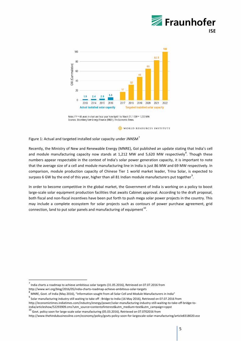
As is the case with all developing nations, the provision of electricity is critical to their energy and economic outlook owing to the coupling of GDP growth with energy demand. India’s electricity consumption as of March 2015 was about 939TWh up from 376TWh in the year 20005. On the supply side as per the Ministry of power, the country currently has an installed capacity of 303GW. The current installed grid connected solar power capacity as of 31 May 2016 is about 7.5GW of the targeted 100GW by the year 2022 under the NSM 6. Of the 100GW, the government plans to have 60GW of ground mounted medium and large scale solar PV projects and the other 40GW to be fulfilled by grid connected rooftop solar PV projects2. Figure 1 shows the breakup of the year-wise targets from 2013 to 2022.
2 Gazette of India, Extraordinary (August 2015), “Scaling up of Grid Connected Solar Power Projects from 20,000 MW by the year 2021-22, to 1,00,000 MW by the year 2021-22 under National Solar Mission” 3 Press Information Bureau, Govt. of India (October 2011), “National Manufacturing Policy” 4 International Energy Agency (2015), “India Energy Outlook – World energy outlook special report” 5 CEA, Govt. of India (April 2015), “Growth of Electricity Sector in India From 1947-2015” 6 MNRE, Govt. of India (May 2016), “Commissioning Status of Grid Connected Solar Power Projects under JNNSM as on 31-05-2016”
5
Figure 1: Actual and targeted installed solar capacity under JNNSM7
Recently, the Ministry of New and Renewable Energy (MNRE), GoI published an update stating that India’s cell and module manufacturing capacity now stands at 1,212 MW and 5,620 MW respectively8. Though these numbers appear respectable in the context of India’s solar power generation capacity, it is important to note that the average size of a cell and module manufacturing line in India is just 86 MW and 69 MW respectively. In comparison, module production capacity of Chinese Tier 1 world market leader, Trina Solar, is expected to surpass 6 GW by the end of this year, higher than all 81 Indian module manufacturers put together9.
In order to become competitive in the global market, the Government of India is working on a policy to boost large-scale solar equipment production facilities that awaits Cabinet approval. According to the draft proposal, both fiscal and non-fiscal incentives have been put forth to push mega solar power projects in the country. This may include a complete ecosystem for solar projects such as contours of power purchase agreement, grid connection, land to put solar panels and manufacturing of equipment10.
7 India charts a roadmap to achieve ambitious solar targets (31.05.2016), Retrieved on 07.07.2016 from http://www.wri.org/blog/2016/05/india-charts-roadmap-achieve-ambitious-solar-targets 8 MNRE, Govt. of India (May 2016), “Information sought from all Solar Cell and Module Manufacturers in India” 9 Solar manufacturing industry still waiting to take off : Bridge to India (16 May 2016), Retrieved on 07.07.2016 from http://economictimes.indiatimes.com/industry/energy/power/solar-manufacturing-industry-still-waiting-to-take-off-bridge-to-india/articleshow/52293909.cms?utm_source=contentofinterest&utm_medium=text&utm_campaign=cppst 10 Govt. policy soon for large-scale solar manufacturing (05.03.2016), Retrieved on 07.0702016 from http://www.thehindubusinessline.com/economy/policy/govts-policy-soon-for-largescale-solar-manufacturing/article8318020.ece

6
3. The PV Value chain and minimum size requirements
The following section briefly describes the generic PV value chain and a theoretical framework for vertical integration followed by a description of the minimum size requirements for each value chain step. The photovoltaics value chain tracks all the distinct processes required to build a PV system. The raw material of most solar cells today is crystalline silicon. Luckily, silicon is one of the most widely available elements on the Earth in the form of sand. Before silicon can be cut into thin wafers, however, it has to be purified, as otherwise the photovoltaic effect will not be very efficient. In the case of crystalline silicon modules, it involves reducing sand to raw silicon followed by purification, wafer cutting, doping, cleaning and coating to form cells. These cells are subsequently connected and laminated to form a module, which is to be assembled in an array and combined with electrical components to make a system. Figure 2 below shows a Si-based PV manufacturing standard production process in different primary segments.
Figure 2: Standard Si-based PV module production value chain11
3.1 Vertical Integration
Vertical integration can occur in two different directions, downstream or upstream. Downstream, also called forward vertical integration, involves controlling of final products and wholesaling operations to deliver the products to customers. Through downstream vertical integration, performance of the company improves due to greater influence on customer demand. On the other hand, upstream, also called backward vertical integration includes ownership and production of the raw materials that are normally bought from external producers. It is an effective way to ensure the availability of the raw materials. Vertical integration may be full or partial. Full integration means that all of the first stage’s production is transferred to the final stage without any sales or purchases to/from third parties in transitional stages. It is called partial integration if stages of production are not sufficient enough to reach the final good without a third party intervention.
A single company can produce the complementary products of different production stages more efficiently than would several firms. Such companies present economies of vertical integration, meaning that the total cost of producing the same good is lower in a vertically integrated structure. According to Garcia et al.12 sources of economies of vertical integration are technological economies, transactional economies and economies resulting from inefficient input allocation. Technological economies stem from physical interdependencies in the production process which implies that costs can be reduced if integration of firms results in a closer geographic proximity of production units. Transactional economies are dependent on coordination costs, covering costs due to negotiations and contracts with suppliers and buyers. In a vertically integrated company, transaction costs are expected to be lower. The third source of economies of vertical integration is the upstream direction. If there are important scale economies at the production stage, the
11 Skumanich, A. (Ed.), 2009. Vertical Integration in the PV Industry: 2010 and beyond, 6 pp 12 Garcia, S., Moreaux, M., Reynaud, A., 2007. Measuring economies of vertical integration in network industries: An application to the water sector. International Journal of Industrial Organization 25 (4), 791–820.
7
upstream companies will benefit from larger profit margins. In addition to this, they are more protected against market imperfections on the raw material supply side.
Both vertical integration directions have pro’s and con’s. The main advantage of achieving an upstream vertical integration is being able to control and assure the availability of supply of the raw materials. Because of the lack of adequate polysilicon for the existing demand in the past, it came out that the best business model was an upstream integration with in-house polysilicon production.
Other main advantages of upstream integration include:
- lower production costs,
- cost savings due to improved optimization over the entire production chain,
- opportunity to add margins to each production segment,
- faster responses to market changes along the full chain,
- reduced working capital and
- no long-term purchase contracts and up-front securing payments.
The main disadvantage of vertical integration is that the completely diversified structure of the company might create potential issues of matching both the output and quality of the materials along the chain. Each segment must be tuned to provide the optimum quantity and quality needed without a shortage or surplus. Other risks can be increased organizational complexity, higher investment costs and less flexibility when market requirements change.
3.2 Status of chosen technology
This section details the status of the current technology in the market based on industry standards, what might be the most realistic trend within the industry within the next two years and ends with an exemplary technology choice based on these technologies for the different value chain steps starting from poly-Si production up to module assembly.
Beginning with crystallization techniques, p-type (Boron doped) block casting of multi-crystalline Silicon (mc-Si) is the most widespread and represents the major technology compared to p-type mono-crystalline Silicon. GCL poly from China is the largest manufacturer with more than 10GW of annual production capacity for p-type mc-Si. In the case of mono-crystalline Silicon, large players like Longi (China) are pursuing the production of p-type mono-Si, especially for high efficiency PERC cells.
As wafering technology, Multi-Wire Slurry Sawing (MWSS) for mc-Si and Diamond wire sawing for mono-Si is becoming standard. The adaption of Diamond-Wire to mc-Si is currently a major task for industrial R&D as it offers a large cost reduction potential. Kerf less cutting and new casting methods such as either direct solidification (e.g. 1366 Technologies) or Epitaxial wafer growth (e.g. CrystalSolar, NexWafe) are moving from R&D to pilot production phases as they offer principal cost advantages by avoiding energy intensive casting as well as any kerf loss. For mc-Si then, Multi-Wire Slurry Sawing still represents the state-of-the-art technology, as more cost effective Diamond Wire sawing (already widely used for mono-Si) still faces yield issues when applied for mc-Si.

8
For the cell technology, presently 70 to 80% of existing capacity is based on standard Aluminium-Back surface field (Al-BSF) technology, but the upgrade of existing lines to Passivated Emitter and Rear Contact (PERC) cell is rapidly ongoing and most probably will replace the commonly used Al-BSF technology as “Standard” cell technology. The total PERC capacity has already surpassed 10GW of capacity worldwide. High efficiency technologies like Heterojunction technology (HJT) by Panasonic or Back-Junction Back-Contact (BJ-BC) by SunPower focus on markets with high area related installation cost (for instance, the roof top market in Japan) where power per area is critical.
In the case of module technology, the standard glass/backsheet modules with 3 Busbars standard solder stringing technology represents the state-of-the-art. Manufacturers are currently moving towards 5 Busbars in order to reduce the series resistance losses and hence improve Cell-to-Module (CTM) losses. Glass-glass modules enable ‘bifaciality’ of cell and module technology and offer higher mechanical stability resulting in longer guaranteed module lifetimes (30 instead of 25 years). Different interconnection technologies like Multi-wire stringing are emerging, offering electrical as well as optical advantages (e.g. LG is using this technology within their latest highest power module series).
Technology Selection criteria
Siemens rod based CVD direct chlorination or hydrochlorination
- Most widely used technology for new market entrants
- Well proven technology - Choice depends on investors background and
existing infrastructure
Boron-doped (p-type) mc-Si ingot +
Multi-wire slurry sawing (MWSS)
- p-type silicon wafer material is by far the most convenient silicon wafer material, technical improvements like the High Performance mc-Si approach lead to even higher quality silicon material and high silicon utilization
- MWSS most suitable technology for mc-Si with highest production yield
PERC solar cells - PERC cells have a much higher efficiency
potential than Al-BSF cells, especially with constantly decreasing wafer thicknesses (below 120µm it might be even impossible to manufacture Al-BSF cells without significant yield loss due to wafer warpage).
- Within the next 2 to 3 years, PERC cell technology will be more and more the standard cell technology globally.
EVA based Glass-Backsheet modules
- Most widely used technology for market entrants - Proven bankability of the modules - Simple upgrade towards Glass-Glass technology
possible (prolonged product warranties of 30 years)
Figure 3: Exemplary technology choice based on current state-of-the-art technologies for the different value chain steps starting from poly-Si production up to module assembly.

9
3.3 Minimum size requirements and definition of cases
This section describes the minimum size requirements for each production step for economic viability as well as defines the cases studied for arriving at the individual step and total production costs.
Table 1 below summarizes the economic reasonable minimum production capacity requirements for mg-Si and poly-Si production as well as capacities for wafers, cells and modules in case of a full-blown vertically integrated crystalline silicon PV production value chain. The economically sound production capacity for mg-Si of 35,000 tons/year exceeds the needs for the local PV manufacturing by nearly a factor of three; however, the resulting end product can be sold to different other end user markets. As a consequence, the decision to integrate or not to integrate an mg-Si production into a project has to be detached from the considerations related to the PV market. Most probably also, different investors would have to be attracted as the technology and markets are quite different when compared to the PV value chain.
A minimum plant size for standard Siemens based poly-Si production is 10,000 tons/year, with such an amount of poly-Si either the full downstream chain for wafers, cells and modules, resulting in an overall production capacity for modules of more than 1.7 GW, is supported, or the poly-Si feedstock material is sold to other customers on local or worldwide markets. In this study, the aim is to provide an outlook for a production capacity for 100MWp and 1GWp of wafer, cell and module manufacturing as detailed above. From the initial investment, the poly-Si production represents the most capital investment and power intensive part of the entire crystalline PV value chain.
Sector Production capacity
Investment costs (INR Crore) Comment
Metallurgical-Silicon (mg-Si) 35,000 tons 1,250 – 1,50013
Minimum plant size; 13,000 tons for PV and 22,000 tons sold to other industries
Polysilicon (poly-Si) 10,000 tons 2,200 – 2,500 Minimum plant size, range based on low and high case
Wafer 100MWp 140 – 200 Range based on low
and high case 1GWp 900 – 1,140
Cell 100MWp 120 - 170 Range based on low
and high case 1GWp 770 - 920
Module 100MWp 70 - 100 Range based on low
and high case 1GWp 450 - 580
Table 1: Overall production capacities of wafers, cells and modules for the realization of the complete PV value chain starting based on minimum size requirements for poly-Si production.
13 Adapted from Solar Cluster Baden-Württemberg, 2015, “Green Silicon” Feasibility of fully vertically integrated photovoltaic module production in Brazil and Paraguay (pg 61)
10
It has been established that the saturation of economy of scales is being reached for a high level of production capacities for the production of metallurgical silicon. Companies which invested into this level of capacity are now able to take profit from the respective advantages. To compete with this benchmark, in the context of this study, the authors use a capacity of 35,000 tons for mg-Si based on existing studies14. However, the silicon produced could be sold to industries other than photovoltaics. Additionally, the by-product silica fume, applied in the construction industry, could also be sold for approximately 6700 INR/ton (100 $/ton).
For polysilicon the economic viability is reached at a lower level. However, according to technical research, at least 10,000 tons of production capacity is considered to be the minimum. For that, approximately 13,000 tons of mg-Si is necessary. The difference of 22,000 tons mg-Si is considered to be sold on the market, either for photovoltaic purposes or for other industries as mentioned above.
The main building blocks for the unit production costs of metallurgical grade silicon and polysilicon are capital investment needs, procurement costs for raw materials, chemicals and other media as well as continuous improvement and learning-curve assumptions over the useful life of the projects. For the first two sets, capital investments and procurement of main resources, ranges were applied in order to derive a low- and high-cost estimate for unit-production costs. Also, the number of working hours in a year were varied from 8520 hours or high (100%) utilization to nearly 6000 hours or low (70%) utilization (in actual 5964 hours), which is assumed as the average number of hours worked in a year in India for traditional manufacturing plants, in order to compare the effect of higher utilization rates on production costs for both production capacities (100MWp and 1GWp) for wafer, cell and module manufacturing. It is important to highlight that the reduced working hour utilization actually really produces less output with the same CAPEX spending. As a result, a manufacturer who sticks to lower or ‘traditional’ working hours (70% utilization case) has to spend more CAPEX for maintaining similar output (100MWp or 1GWp) than other competitors with 100% utilization as is the case with global manufacturers.
It was found that while module, cell and wafering production are already economically sound at relatively small production quantities below 500 MW, ingot manufacturing or even more significant poly-Si production starts to be economically meaningful at production capacities above 1 GW. The values described above are to be considered as a scenario for full coverage of the entire value chain from metallurgical silicon to finished photovoltaic modules. For each individual process step a decision has to be made whether to buy or to make products in own facilities. For metallurgical silicon and for polysilicon the volumes assumed are the minimum output capacity whereas for all three following process steps it could be an option to reduce the production throughput and to sell spare products on market.
The cases are defined as
- “Low case”: represents the most relevant consumables per value chain production step at preferential prices usually available from direct local supply.
- “High case”: most relevant consumables per value chain production step at prices from world market (mostly imported) or at high local prices.
- “High (100%) utilization”: 8520 working hours a year for international standard 24/7 production.
- “Low (70%) utilization”: 6000 working hours a year based on traditional Indian manufacturing plants.
14 Solar Cluster Baden-Württemberg, 2015, “Green Silicon” Feasibility of fully vertically integrated photovoltaic module production in Brazil and Paraguay (pg 90-91)

11
As a result for wafer, cell and module production considering the above four cases based on capacity size range of 100MWp to 1GWp with 100% and 70% utilization (based on number of working hours which drops the net output to 70MWp and 700MWp respectively) along with the low and high cost case range for capital investment and procurement of main resources, eight cases were studied to arrive at resultant production costs for each step as well as All-in-module production costs for the entire value chain. The All-in-module costs for the lowest production cost case were further investigated by applying a scaling factor to derive the effect of economy of scales (EoS) on the total production cost.
3.4 Degree of Automation
The motivation to fully automate the production lines is not just the reduction of labor costs: automation can also ensure increased production capacities and significantly improve the product quality, especially as the final product quality influences strongly the net profits of the entire company. Additionally, manufacturing efficiency can be enhanced and ramp-up phases shortened at the same time. Since factories are flexible and capacities are on the increase, the effort involved in adapting automation to the needs of growth can be planned and realized more easily than the effort required to organize larger amounts of manual work.
Handling procedures for (un-)loading and transportation can be optimized and process steps assessed individually. Manual handling is a non-measurable procedure that cannot be repeated exactly and is highly dependent on the person concerned. Ever-increasing throughput and reliability require a high repetition of simple and complex tasks with constant precision. In theory, simple tasks executed manually should have a low failure rate. But, in practice, doing the same, repetitive task for eight hours or more is extremely tedious, making it difficult to concentrate throughout the entire period, with the result that failure rates are higher than expected. An adapted, optimally balanced automation solution can help to minimize problems associated with wafer breakage or quality defects such as micro-cracks, and thus improve yield and quality. When (un-)loading wet chemistry equipment, operators are exposed to the risk of injury from caustic fluids or vapors. The use of automated systems can reduce the risk to increase the safety at work.
In contrast to semiconductor industry, PV manufacturing does not require sophisticated clean-room conditions. Nevertheless, studies in the past have shown that the use of mini-environments for dedicated process steps could increase the overall efficiency of the final product. An example in that sense is the loading and unloading area of the high temperature diffusion furnaces, where automaton combined with a dedicated mini-environment will result in higher process qualities (fewer impurities incorporated during diffusion steps and prior to subsequent surface passivation).
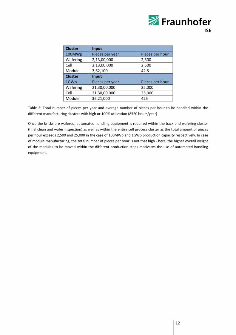
For the PV manufacturing clusters (wafer, cell, module) different degrees of automation might be foreseeable. This is reflected by the average goods per hour to be handled within the different clusters as can be seen in Table 2.
12
Cluster Input 100MWp Pieces per year Pieces per hour Wafering 2,13,00,000 2,500 Cell 2,13,00,000 2,500 Module 3,62,100 42.5 Cluster Input 1GWp Pieces per year Pieces per hour Wafering 21,30,00,000 25,000 Cell 21,30,00,000 25,000 Module 36,21,000 425
Table 2: Total number of pieces per year and average number of pieces per hour to be handled within the different manufacturing clusters with high or 100% utilization (8520 hours/year)
Once the bricks are wafered, automated handling equipment is required within the back-end wafering cluster (final clean and wafer inspection) as well as within the entire cell process cluster as the total amount of pieces per hour exceeds 2,500 and 25,000 in the case of 100MWp and 1GWp production capacity respectively. In case of module manufacturing, the total number of pieces per hour is not that high - here, the higher overall weight of the modules to be moved within the different production steps motivates the use of automated handling equipment.
13
4. Cost Analysis of PV value chain
The Indian solar manufacturing sector is still small in scale and more fragmented leading to higher costs. The less technologically developed and small sized manufacturing industry limits its market ability, and focuses only on parts of the manufacturing supply chain; thus hampering attempts to achieve economies of scale resulting in higher production costs. Single module manufacturing lines globally start to produce at capacities around 100 to 150 MW. Such a scale allows the potential for procuring raw materials and the option of increasing production without constantly incurring investment costs for line expansions. However, in India, recently set up module lines are still smaller in capacity, forcing companies that wish to raise production to frequently make production line investments that result in a higher price per watt. Such a small scale manufacturing also leads to lower quality products. As mentioned in Section 2, the average size of a cell and module manufacturing line in India is just 86 MW and 69 MW respectively. It is important, though, to note that as of this year, announcements have been made of several companies such as Adani Power, Tata Power, Vikram Solar and so on targeting a larger production scale in the country by either new investments into the PV manufacturing sphere - Adani Power, for instance, is setting up a 1.2GW cell manufacturing facility that could be operational by early next year15 – or by increasing existing manufacturing facilities.
Manufacturers also face other systemic limitations such as poor infrastructure, lack of raw materials, an undeveloped supply chain, and lack of financing etc. hence the market demand is extremely poor. This makes the financial viability of manufacturing extremely circumspect. After Service is also an area of concern for customers, who are not aware how this works and indeed, the framework is still not in place.
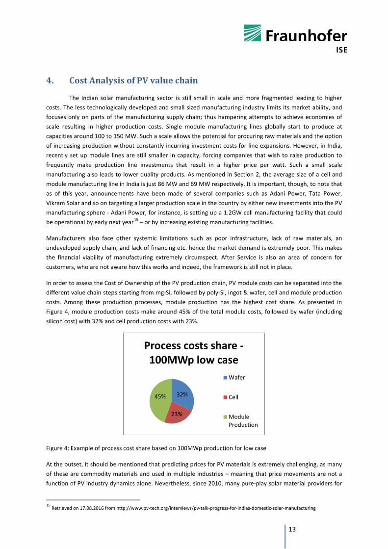
In order to assess the Cost of Ownership of the PV production chain, PV module costs can be separated into the different value chain steps starting from mg-Si, followed by poly-Si, ingot & wafer, cell and module production costs. Among these production processes, module production has the highest cost share. As presented in Figure 4, module production costs make around 45% of the total module costs, followed by wafer (including silicon cost) with 32% and cell production costs with 23%.
Figure 4: Example of process cost share based on 100MWp production for low case
At the outset, it should be mentioned that predicting prices for PV materials is extremely challenging, as many of these are commodity materials and used in multiple industries – meaning that price movements are not a function of PV industry dynamics alone. Nevertheless, since 2010, many pure-play solar material providers for
15 Retrieved on 17.08.2016 from http://www.pv-tech.org/interviews/pv-talk-progress-for-indias-domestic-solar-manufacturing
32%
23%
45%
Process costs share -100MWp low case
Wafer
Cell
ModuleProduction

14
the more commodity-like items such as slurry and EVA have emerged, especially in China, and these materials have experienced an oversupply environment similar to that of solar-specific components. This has resulted in significant price reductions, to the point where pricing for many of these items is currently at levels close to cost.
As with polysilicon, there is significant uncertainty about the future trend of consumables pricing. On one hand, materials suppliers will continue to experience pressure to continue reducing prices from their component customers so as to enable further cost reductions at the module level. On the other hand, unlike solar-specific components, the manufacturing technology for most of these materials is fairly mature, meaning that the cost floor is fairly fixed aside from gains from scale, unless lower-cost or more innovative alternatives can be found.
In the following sub-chapters, a more detailed cost analysis of the individual value chain steps is shown. Such an analysis will be important in case of the need to sell intermediate products on the market (which will be anyhow true in case of mg-Si, as the capacity is much larger than needed for the PV value chain). The cost evaluation is carried out with the help of a cost model – the SCost COO Calculation tool aligned with the SEMI Cost of Ownership standards developed by Fraunhofer ISE16. The SCost tool allows for bottom-up simulation of the industrial production of c-Si wafers, cells and modules along the PV value chain. The production input data for the tool is obtained from equipment manufacturers, cell and module manufacturers, material suppliers and other ISE project partners. In the Indian context, contacting local suppliers of critical raw materials for both cell and module manufacturers will be key to obtaining raw material cost input data for the tool. In the case of non-availability of suppliers, either import costs of said material will be used or a sensitivity analysis will be performed with existing global prices to arrive at Indian module manufacturing costs. Other input parameters such as labor, energy price and financial costs are based on the prevailing local conditions and are mostly transferrable across Indian industry sectors.
The static assumptions relating to depreciation periods and annual gross salaries followed by the wafer, cell and module specifications are outlined below:-
Common static assumptions17
Electricity cost 5.5 INR/KWh Capex equipment 30% Capex building, facilities, infrastructure, auxiliaries 70%
Equity share 20% Equity interest rate 20% Debt interest rate 12.5% Corporate tax18 34.61% WACC (Calculated) 10.54%
Depreciation period – equipment 7 years Depreciation period – building, facilities, infrastructure, auxiliaries 25 years
16 Sebastian Nold (March 2016), Fraunhofer ISE, “Cost of Ownership Analysis of Silicon PV technologies” 17 Price assumptions taken from Policy note, CSTEP (Mar 2016), “Polysilicon Manufacturing in India: Go or No-Go” 18 Retrieved on 17.08.2016 from https://home.kpmg.com/xx/en/home/services/tax/tax-tools-and-resources/tax-rates-online/corporate-tax-rates-table.html

15
Labour19 Annual gross salary Operator 1,20,000 INR Technician 1,80,000 INR Engineer 3,60,000 INR Administration 2,40,000 INR Scientist 4,80,000 INR
Wafer/Cell/Module specifications Wafer size 156.65*156.65 mm2
Wafer thickness 180 µm
Cell type p-type multi-crystalline PERC cell Cell efficiency 19.39 % Cell power 4.76 Wp
Module type EVA-Glass-Backsheet module Module efficiency 17.4 % Module power 285.9 Wp
4.1 Cost structure of each value chain step – Metallurgical-Silicon (mg-Si) and Polysilicon
The production of metallurgical silicon takes place in large open submerged arc electric furnaces (“EAF”) using three large carbon based AC (alternating current) electrodes. The process has been industrialized over the last century and the basic process has not changed significantly. This is a function of the specific conditions in which quartz transforms to SiO gas and combines with carbon, which are reproducible in a unique furnace environment. The process takes place in very rustic and industrial conditions and is highly energy intensive, on the order 12 to 14 MWh per mg-Si ton of output, which is concentrated mainly in the reduction step due to the need to disassociate highly stable silicon oxides in the form of quartz into the final product.
This process is accompanied by an intense emission of gases with high content of CO2 and entrained particulates that should be treated in an appropriate manner which also represents a high loss of energy. The off gas must be captured by a dust removal system before being released into the air, and can be sold as a byproduct called “silica fume”. The heat from the process can be captured and reused for pre-heating of ladles and other equipment.
The energy intensive parts of the crystalline silicon photovoltaic value chain, namely the upstream production of metallurgical grade silicon and polysilicon, are also capital intensive production processes, as evidenced by the fact that roughly 50% of the unit production costs are comprised by electricity and depreciation charges. For this reason, locations that offer globally competitive electricity rates from environmentally sustainable sources, offer a particularly compelling investment case for the production of the energy and capital intensive silicon feedstock.
19 Assumption for annual labour prices based on average Indian wages for the different types of labour mentioned
16
As discussed in section 3.3, the minimum economic viable size for mg-Si production is that of 35,000 tons per year of which 13,000 tons are used as feedstock for polysilicon production. The capital investment costs for a metallurgical-Silicon plant for this study are estimated based on global values of existing plants. It is important to note, however, that the key cost drivers for mg-Si production such as quartz (feedstock), coal, wood chips and electrodes are all available in India (or can be imported) and hence the capital costs could be lower based on their prices.
The procurement cost ranges adopted for capital investment needs for the metallurgical silicon plant based on global price estimates are:- Capex20 1,250 – 1,500 INR Crore
Polysilicon is produced using metallurgical grade Silicon (mg-Si) as a feedstock material. While mg-Si has a purity of 98-99% Silicon, the photovoltaic and semiconductor industries have much higher purity requirements, namely at least 99.9999% (6N) and 99.9999999% (9N) for photovoltaics and for semiconductor usage, respectively. This is due to the properties of semiconductors which can be precisely engineered if the basic material is of high enough purity. Using very pure silicon, as well as traces of elements of the third and fifth main group in the Periodic Table, mainly boron and phosphorous (but as well indium, arsenic and antimony), transistors and diodes and other electronic devices can be manufactured and tailored.
There are different variants of the Siemens method currently in use on an industrial basis. Common to all of them is that in the first step, Trichlorosilane (TCS) is produced from mg-Si. This is then purified by distillation and then with some intermediate steps, deposited again as pure silicon in a deposition reactor. These variants differ in the way of TCS formation (hydro chlorination vs. direct chlorination), starting material for deposition (TCS vs Monosilane) and deposition method (24, 36 or more pair reactor vs. fluidized bed reactor). All the mainstream methods have their strength and weaknesses and the choice of which one is used is dependent on a variety of variables (energy supply, infrastructure, size, quality, labor, supplies, etc.).
In the case of polysilicon manufacturing, recently the Centre for Study of Science, Technology and Policy (CSTEP), India performed a feasibility study for domestic polysilicon manufacturing in India21. The study proposed that India should establish a 24,000 TPA indigenous polysilicon manufacturing plant which can potentially support 5GW of annual solar PV module production at a cost of approximately INR 5,500 crore which would require private investors to form a consortium to finance this high capital cost. The study found that the cost of indigenously manufactured polysilicon works out to INR 1,340/kg (USD 20/kg) with the main cost components being Interest and depreciation (50%) and energy (20%).
The study further examined scenarios wherein the government provides support by enabling low cost financing with lower interest rates and reliable and low-tariff power by providing a dedicated power plant, say Hydro, for polysilicon production, similar to that practiced in China. These scenarios lead to a reduction in the cost of indigenous polysilicon to a best case value of INR 944/kg (14 USD/kg). The results of this study were used as the input ranges as a starting point for polysilicon prices for the rest of the PV value chain i.e. polysilicon feedstock to module production. Figure 5 shows the breakdown of production costs for the case of polysilicon adapted from the CSTEP study.
20 Refer Section 3.3 & Table 1 21 Policy note, CSTEP (Mar 2016), “Polysilicon Manufacturing in India: Go or No-Go”

17
The procurement cost ranges for main cost drivers and capital investment needs for the metallurgical silicon plant are outlined below:
Key cost driver low case high case unit Interest 6 12,5 % Electricity 0,75 5,5 INR/kWh
Capex22 2,200 – 2,500 INR Crores
Figure 5: Net polysilicon production costs based on scenarios from CSTEP study
The procurement cost ranges for major resources are, in both instances, likely to be achievable. However, further work on supply-conditions is needed in order to narrow the projection range and thereby reduce the level of uncertainty. Also, the capital investment cost ranges are thought to reflect best-in class ranges for the facilities under investigations. However, some level of uncertainty remains as the project related capital investments are highly dependent on the conditions of the eventual production sites, e.g. amount of levelling needed, type of foundation (shallow or pile), distance to utility connection points as well as negotiated construction, facility and equipment prices.
4.2 Cost structure of each value chain step – Ingot and Wafer
The manufacturing flow for mc-Si ingot and wafer production consists of three major process steps:
- Ingot Production Line
- Brick Production Line
- Wafer Production Line
Polysilicon chunks are received from the polysilicon supplier in double PE (polyethylene) bags. Quality control is performed by the polysilicon supplier and hence specification and quality certification are delivered by the polysilicon supplier. Only material which meets the specifications should be accepted for the ingot line in order
22 Capex estimated as: 24,000 TPA costs 5,500 INR Cr which implies that 10,000 TPA costs (5,500/24,000)*10,000 = 2,300 INR Cr (approx.)
268 422,1
40,2
281,4 636,5
636,5 944,7
1340
0
200
400
600
800
1000
1200
1400
1600
Low Case High CaseNet
pol
ysili
con
prod
uctio
n co
sts
(INR/
kg)
Net polysilicon production costs
Depreciation, Labour &raw material
Electricity
Interest
Total cost

18
to avoid damage to the equipment, ensuring the required quality and product yield. Re-melt silicon materials (squaring parts, bottoms or side walls) are received from the in-house silicon recycling.
The crucibles are delivered with coated silicon nitride. The coated crucibles are inspected and subsequently manually filled with polysilicon and re-melt silicon in a skilled way in order to allow maximum charge of polysilicon in the crucible with minimal contamination. Adequate amount of doping material has to be added to the polysilicon to achieve the required electrical resistivity. The dopant can either be added in the form of pure boron or in the form of heavily boron doped silicon chips. In both cases the dopant amount, which has to be added to the polysilicon into the crucible must be calculated. For this purpose an adequate scale must be available and regularly calibrated. Finally the supporting graphite plate walls have to be mounted around the crucible and this whole set-up will then be covered with a lid before it is ready to be moved to the Crystallization Furnace.
The filled crucible is mounted into the Crystallization Furnace, the lid is removed and the furnace is closed. After heating and melting the silicon in the furnace, the melt is actively cooled down slowly from the bottom to the top of the crucible (crystallization process). Thus, multiple crystalline silicon grains grow from the bottom to the top and form the multi-crystalline silicon ingot. Impurities in the silicon melt are transported upwards inside the melt due to segregation coefficient (segregation coefficient = difference in solubility of impurities atoms in liquid to that in solid). Therefore the top layer of the ingot usually contains a relatively high concentration of impurities (like iron, nickel, copper and carbon) and needs to be cut off and scrapped.
This silicon ingot produced has a size of approximately 84 x 84 x 27 [cm] with a total mass of about 450kg. With adaptations to the equipment the ingots size can be extended to approximately 99 x 99 x 27 [cm] with a total mass of about 620 kg. As per the latest ITRPV roadmap, ‘Generation 6’ ingoting is mainstream today with ingot masses greater than 700kg.23
After the ingot has cooled down to a temperature below 300°C, the furnace is opened and the crucible with the ingot is taken out. It is transferred to a special cooling area where the graphite support material and the crucible is removed from the ingot. Any residues coming from the crucible wall on the ingot are removed.
The fully automatic brick production process consists of the following steps:
- Loading of ingot into first diamond wire cutting unit
- Cutting of ingot into slabs
- Automatic transfer of slabs to second cutting unit
- Cutting of slabs to bricks
- Transfer of bricks to brick line conveyor
The cut-away sidewalls of the ingot will be recycled for the production of multi-crystalline silicon ingots (Silicon Recycling).
23 International technology Roadmap for Photovoltaic (ITRPV) 2015 Results, Seventh Edition, March 2016
19
Wafer slicing, also called “wafering,” is a key part of the solar photovoltaic (PV) cell manufacturing process. The process begins with solid ingots made of single-crystal or multi-crystalline silicon material. Wire saws are then used to shape the ingots into squared blocks and slice them into thin wafers. The conventional wire sawing technique uses a very thin, high strength steel wire which carries the slurry that performs the cutting action. The wire is wound on guides that form a horizontal “web” of up to 1,000 parallel wires. Motors rotate the wire guides, causing the entire wire web to move at a speed of five to 25 meters per second. The wire speed and its linear (back and forth) motion are adjusted throughout the cut. Nozzles continuously spray the moving wires with slurry that typically contains suspended silicon carbide particles. The silicon blocks are mounted to cutting tables. The cutting tables then travel vertically through the moving wire web, cutting the blocks into wafers. While this is a mature process, it has significant consumables costs, driven by slurry and wire usage. Manufacturers are adopting recycled slurry in increasing mix percentage as a primary way to reduce consumables costs.
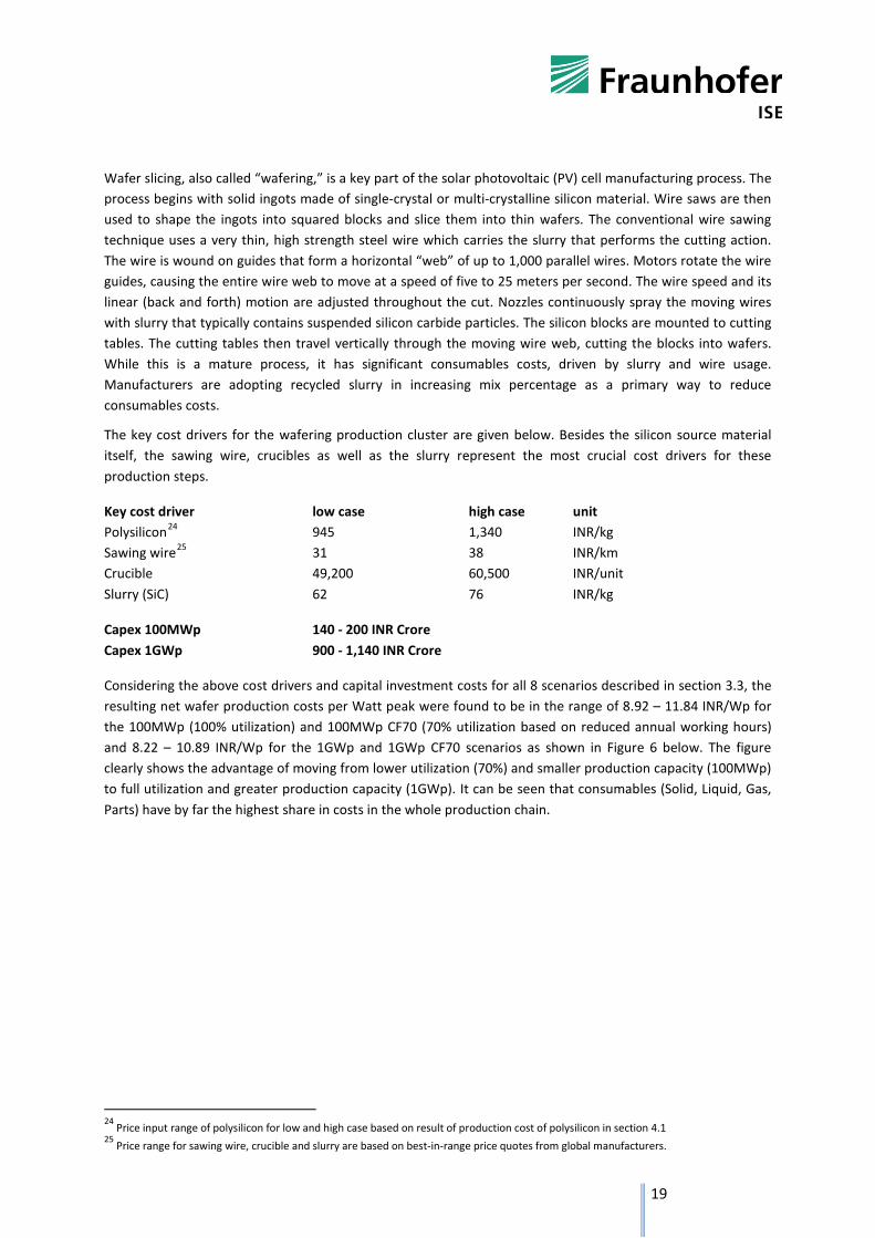
The key cost drivers for the wafering production cluster are given below. Besides the silicon source material itself, the sawing wire, crucibles as well as the slurry represent the most crucial cost drivers for these production steps.
Key cost driver low case high case unit Polysilicon24 945 1,340 INR/kg Sawing wire25 31 38 INR/km Crucible 49,200 60,500 INR/unit Slurry (SiC) 62 76 INR/kg
Capex 100MWp 140 - 200 INR Crore Capex 1GWp 900 - 1,140 INR Crore
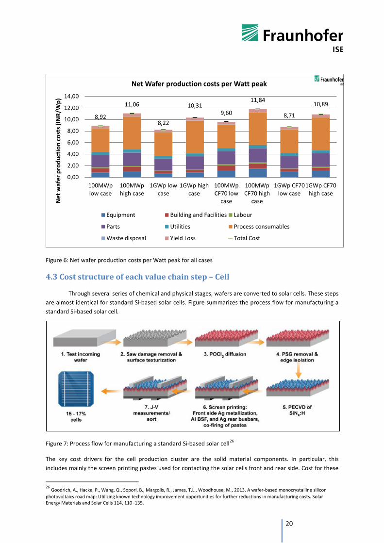
Considering the above cost drivers and capital investment costs for all 8 scenarios described in section 3.3, the resulting net wafer production costs per Watt peak were found to be in the range of 8.92 – 11.84 INR/Wp for the 100MWp (100% utilization) and 100MWp CF70 (70% utilization based on reduced annual working hours) and 8.22 – 10.89 INR/Wp for the 1GWp and 1GWp CF70 scenarios as shown in Figure 6 below. The figure clearly shows the advantage of moving from lower utilization (70%) and smaller production capacity (100MWp) to full utilization and greater production capacity (1GWp). It can be seen that consumables (Solid, Liquid, Gas, Parts) have by far the highest share in costs in the whole production chain.
24 Price input range of polysilicon for low and high case based on result of production cost of polysilicon in section 4.1 25 Price range for sawing wire, crucible and slurry are based on best-in-range price quotes from global manufacturers.
20
Figure 6: Net wafer production costs per Watt peak for all cases
4.3 Cost structure of each value chain step – Cell
Through several series of chemical and physical stages, wafers are converted to solar cells. These steps are almost identical for standard Si-based solar cells. Figure summarizes the process flow for manufacturing a standard Si-based solar cell.
Figure 7: Process flow for manufacturing a standard Si-based solar cell26
The key cost drivers for the cell production cluster are the solid material components. In particular, this includes mainly the screen printing pastes used for contacting the solar cells front and rear side. Cost for these
26 Goodrich, A., Hacke, P., Wang, Q., Sopori, B., Margolis, R., James, T.L., Woodhouse, M., 2013. A wafer-based monocrystalline silicon photovoltaics road map: Utilizing known technology improvement opportunities for further reductions in manufacturing costs. Solar Energy Materials and Solar Cells 114, 110–135.
8,92
11,06
8,22
10,31 9,60
11,84
8,71
10,89
0,00
2,00
4,00
6,00
8,00
10,00
12,00
14,00
100MWplow case
100MWphigh case
1GWp lowcase
1GWp highcase
100MWpCF70 low
case
100MWpCF70 high
case
1GWp CF70low case
1GWp CF70high case
Net
waf
er p
rodu
ctio
n co
sts (
INR/
Wp)
Net Wafer production costs per Watt peak
Equipment Building and Facilities Labour
Parts Utilities Process consumables
Waste disposal Yield Loss Total Cost
21
components are amongst the main cost drivers of this part of the value chain, as listed below, prices are highly influenced by the actual price listings of the source metals itself, silver and aluminum. Fluctuations in source metal prices are also the main driver for technology improvements, e.g. the ongoing reduction of the finger width for front metallization of the solar cell or even the development of production technologies to replace of silver by e.g. copper plating, represent the most crucial cost drivers for these production steps.
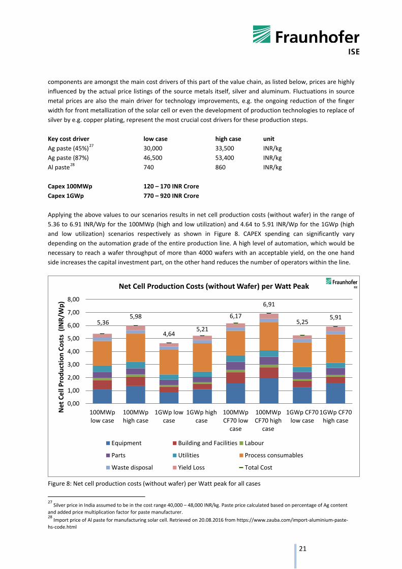
Key cost driver low case high case unit Ag paste (45%)27 30,000 33,500 INR/kg Ag paste (87%) 46,500 53,400 INR/kg Al paste28 740 860 INR/kg Capex 100MWp 120 – 170 INR Crore Capex 1GWp 770 – 920 INR Crore Applying the above values to our scenarios results in net cell production costs (without wafer) in the range of 5.36 to 6.91 INR/Wp for the 100MWp (high and low utilization) and 4.64 to 5.91 INR/Wp for the 1GWp (high and low utilization) scenarios respectively as shown in Figure 8. CAPEX spending can significantly vary depending on the automation grade of the entire production line. A high level of automation, which would be necessary to reach a wafer throughput of more than 4000 wafers with an acceptable yield, on the one hand side increases the capital investment part, on the other hand reduces the number of operators within the line.
Figure 8: Net cell production costs (without wafer) per Watt peak for all cases
27 Silver price in India assumed to be in the cost range 40,000 – 48,000 INR/kg. Paste price calculated based on percentage of Ag content and added price multiplication factor for paste manufacturer. 28 Import price of Al paste for manufacturing solar cell. Retrieved on 20.08.2016 from https://www.zauba.com/import-aluminium-paste-hs-code.html
5,36 5,98
4,64 5,21
6,17
6,91
5,25 5,91
0,00
1,00
2,00
3,00
4,00
5,00
6,00
7,00
8,00
100MWplow case
100MWphigh case
1GWp lowcase
1GWp highcase
100MWpCF70 low
case
100MWpCF70 high
case
1GWp CF70low case
1GWp CF70high case
Net
Cel
l Pro
duct
ion
Cost
s (IN
R/W
p)
Net Cell Production Costs (without Wafer) per Watt Peak
Equipment Building and Facilities Labour
Parts Utilities Process consumables
Waste disposal Yield Loss Total Cost

22
4.4 Cost structure of each value chain step – Module
A solar module in crystalline technology is composed of various different components, such as a front cover, the encapsulation material, the solar cells that are connected with ribbons and tabs, a back side cover, the junction box and in many cases a frame. Figure 9 illustrates the structure of a finished standard PV module.
Figure 9: Structure of a standard PV module29
As already outlined before, the module manufacturing represents the production part with highest cost share (see Figure 4, Section 4). Aluminum module frame, EVA encapsulant, solar glass, junction box and PV ribbon belong to the cost sensitive materials. Mehta analyzed in his work the cost shares of the mentioned materials and the share estimations until 201430. According to the analysis, metal pastes have the highest cost share (used for cell production only) among the other materials, followed by the solar glass, module frame, encapsulates, gases & chemicals and the back sheet. The analysis also found that the prices tend to go down in the future.
Detailed below are the low and high prices for the already mentioned key cost drivers of the module production sequence, aluminum frame, glass, junction box, backsheet and EVA foil31. Especially for the solar glass large differences in prices might exist on the market depending on local availability of solar glass (typically AR coated glass), this would be another reason to consider a potential in-house glass production.
Key cost driver32 low case high case unit Glass 317 477 INR/m2 EVA foil 200 261 INR/m2 Backsheet 272 435 INR/m2 Aluminium frame 520 780 INR/unit Junction box 300 520 INR/unit
Capex 100MWp 70 – 100 INR Crore Capex 1GWp 450 – 580 INR Crore
29 Preu, R., 2012. Solar Energy Part II: Production Technology. REM - PV Elective 1, 2012, University of Freiburg 30 Mehta, S., 2011, PV Bill of Materials Outlook: 2010-2015. GTM Research 31 CSTEP (Oct 2015), “Addressing the Challenges of RE Manufacturing in India : Horizon 2032” (pg 34) 32 Price calculation adapted from CSTEP study. Module power assumed as 260Wp (standard) for calculating price. Size for glass, EVA and backsheet assumed to be 1.636m2 (standard).

23
Figure 10: Net Module production costs (without cell) per Watt peak for all cases
As stated, the resultant cost breakdown in Figure 10 for the net module production costs shows that the largest costs are held by the process consumables. The range varies from 12.48 to 17.46 INR/Wp and from 11.8 to 16.57 INR/Wp for the different 100MWp and 1GWp cases respectively.
4.5 Cost structure of each value chain step – All-in-Module costs
In order to arrive at the all-in-module costs for all the cases based on the key cost drivers and capital investments for each production step provided above, an assumption is made for the S,G&A (selling, general and administrative) costs and R&D (research and development) costs to be 18% of the total net production costs summed for each production step. The resultant all-in-module production costs are shown in Figure 11. It can be seen clearly that the lowest production costs are reached for the 1GWp low case with 100% utilization for a cost of 29.03 INR/Wp. The production cost range for the 100MWp is found to be from 31.66 to 42.41 INR/Wp and for the 1GWp case is from 29.03 to 38.65 INR/Wp. The all-in-module costs without SG&A/R&D costs are the net production costs for each value chain step detailed above (results of Section 4.2, 4.3 and 4.4) summed up for each case.
12,48
16,77
11,80
16,08 13,17
17,46
12,29
16,57
0,002,004,006,008,00
10,0012,0014,0016,0018,0020,00
100MWplow case
100MWphigh case
1GWp lowcase
1GWp highcase
100MWpCF70 low
case
100MWpCF70 high
case
1GWp CF70low case
1GWp CF70high case
Net
Mod
ule
prod
uctio
n co
sts (
INR/
Wp)
Net Module production costs (without cell) per Watt peak
Equipment Building and Facilities Labour
Parts Utilities Process consumables
Waste disposal Yield Loss Total Cost

24
Figure 11: All-in-module production costs per Watt peak for all cases
4.6 Cost structure of each value chain step – Economy of scales effect
A further analysis is made in order to compare the effect of economy of scales on the all-in-module production costs. The economy of scale principle implies that a large production facility would be expected to have a lower cost per unit of output than a smaller facility, all other factors being equal. In the context of the PV industry, economies of scale have an important role. Economies of scale do not only lower the material costs, they also reduce investment costs and increase productivity. Module manufacturers with larger capacities have a higher purchasing and negotiation power against the equipment suppliers and consequently can buy them at lower prices through volume purchase agreements.
There have been several studies conducted on scaling effects in the PV industry. However, quite different results have been reached by several researchers in these studies. The list of the various scaling factors for the PV industry is shown in Table 3 below33
Scaling factor Reference -0,18 Gruber -0,07 Bruton and Woodock -0,20 Ghannam et al. -0,12 Frantzis et al. -0,09 Rohatgi
Table 3: Various scaling factors in PV technology (1997 – 2003) (Yu et al., 2011)
33 Yu, C., van Sark, W., Alsema, E., 2011. Unraveling the photovoltaic technology learning curve by incorporation of input price changes and scale effects. Renewable and Sustainable Energy Reviews 15 (1), 324–337.
26,76
33,81
24,66
31,60 28,94
36,21
26,25
33,38
31,66
39,10
29,03
36,25 34,57
42,41
31,13
38,65
0,00
5,00
10,00
15,00
20,00
25,00
30,00
35,00
40,00
45,00
100MWplow case
100MWphigh case
1GWp lowcase
1GWp highcase
100MWpCF70 low
case
100MWpCF70 high
case
1GWp CF70low case
1GWp CF70high case
All-i
n M
odul
e Co
sts (
INR/
Wp)
All-In Module Costs per Watt Peak
Wafer Cell
Module Production All-in module costs without SG&A/R&D costs
All-in Module Costs

25
For the purpose of the analysis, a scaling factor for the entire production process is taken to be as (-0.069)34 and applied to the 1 GWp low case with 100% utilization (the case with the lowest production cost). The results show a further reduction in the all-in-module production costs of 2.02 INR/Wp as shown in Figure 12 below.
Figure 12: Effect of economy of scales on all-in-module costs per Watt peak for the low cost case
The reduced all-in-module production costs with the scaling factor accounting for economy of scales for the low case scenario are then found to be 27.01 INR/Wp (about 0.40 $/WP). Compared to past and forecasted all-in production cost of modules35 (2011 to 2017) as shown in Figure 13, the resulting all-in production costs are still in a competitive position. Important to note in the figure below is that the price decline over the years is not related to EoS effects but primarily related to strong price declines (5-10%/a).
Figure 13: Forecast of all-in (including COGS, financing and SG&A cost) multi c-Si module cost, best in class
Chinese Producer from Q4-2011 up to Q4-2017
34 Demiray, 2013, “Analysis of the Availability and Scaling Effects of Production Materials on the Production Costs of mc-Si PERC based PV Modules” 35 Mehta, GTM Research, 2013, PV technology and cost outlook 2013-2017
10,19 9,23 8,69
7,40 6,42 6,31
14,07 13,39 12,00
31,66 29,03 27,01
0,00
5,00
10,00
15,00
20,00
25,00
30,00
35,00
100MWp low case 1GWp low case 1GWp low case EoS
All-i
n M
odul
e Co
sts (
INR/
Wp)
All-in Module costs per Watt peak with EoS - low case
Wafer Cell Module Production All-in Module Costs

26
4.7 Sensitivity Analysis
This section shows the effect of important input parameters such as cell efficiency and utilization rates on the all-in-module production costs.
Cell efficiency improvement is found to be the most important driver which brings down the production costs per Watt peak (as more power is available from the same cell area). An efficiency variation was applied for all low cases for both high (100%) and low (70%) utilization to the all-in-module production costs. The results are shown in figure 14 below.
Figure 14: Variation of all-in-module costs with efficiency variation for all low cases.
It is clearly evident from the above figure that cell efficiency improvements or reductions have a substantial effect on the all-in-module production cost per Watt peak. The highlighted data points represent the all-in-module production cost per Watt peak for the chosen cell efficiency of 19.39%.36 With further improvement in cell efficiency values it is possible to reach even lower all-in-module production costs from the currently calculated competitive values in this study.
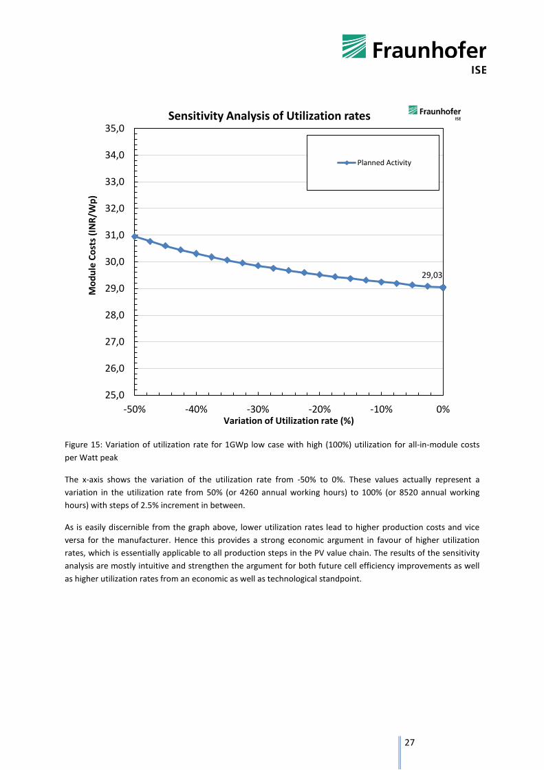
In the case of investigating the effect of variation of utilization rate on the all-in-module production costs, a sensitivity analysis was performed for the 1GWp low case with high (100%) utilization which represented the lowest production costs of 29.03 INR/Wp as detailed in section 4.5. Figure 15 presents the findings of the same.
36 Refer Section 4: Cell specifications
31,66
34,57
29,03
31,13
22
24
26
28
30
32
34
36
38
40
18,0 18,5 19,0 19,5 20,0 20,5 21,0 21,5 22,0 22,5 23,0 23,5 24,0 24,5 25,0
All-i
n-M
odul
e Co
sts (
INR/
Wp)
Cell Efficiency (%)
Efficiency variation for All-in-Module Costs -Low case 100MWp low case100MWp CF70 low case1GWp low case1GWp CF70 low case
27
Figure 15: Variation of utilization rate for 1GWp low case with high (100%) utilization for all-in-module costs per Watt peak
The x-axis shows the variation of the utilization rate from -50% to 0%. These values actually represent a variation in the utilization rate from 50% (or 4260 annual working hours) to 100% (or 8520 annual working hours) with steps of 2.5% increment in between.
As is easily discernible from the graph above, lower utilization rates lead to higher production costs and vice versa for the manufacturer. Hence this provides a strong economic argument in favour of higher utilization rates, which is essentially applicable to all production steps in the PV value chain. The results of the sensitivity analysis are mostly intuitive and strengthen the argument for both future cell efficiency improvements as well as higher utilization rates from an economic as well as technological standpoint.
29,03
25,0
26,0
27,0
28,0
29,0
30,0
31,0
32,0
33,0
34,0
35,0
-50% -40% -30% -20% -10% 0%
Mod
ule
Cost
s (IN
R/W
p)
Variation of Utilization rate (%)
Sensitivity Analysis of Utilization rates
Planned Activity
28
5. Overview of Stimulants and Obstacles for Building-up a PV Industry
This section will compile experience with developing a PV industry in Germany and other relevant PV markets37. The major stimulants and obstacles will be identified and discussed for developing a PV industry. This includes legal framework and political conditions, climate for investments or skilled work force. However, stimulants and obstacles are partially interchangeable, i.e. the lack of incentives may create a barrier and vice versa.
On the worldwide PV market over-capacities of module production have recently decreased, but still persist. Thus, in the global PV market there remains a high level of competition with continued high price pressure, which is determined in particular by the high production capacity in China resp. Asia and their pricing policy. Therefore new module manufacturers entering the market either need to compete globally with the price benchmark of Chinese modules and cells or ensure to provide a stable domestic sales market.
5.1 Stimulants
- Stable domestic market
The importance of a stable domestic PV sales market can be illustrated by the recent developments in the European Union. While PV installations boomed until 2012 in Europe, installations dropped sharply in 2013 with 40 % less installations than in the previous year. Particularly demand from large markets in Europe, such as Germany or Italy, diminished by 60 % compared to 2012. Thus in 2013, the global PV demand had continuously and increasingly shifted from Europe to Asia and the USA. With shrinking demand in Europe and increasing cost pressure due to Asia’s cheap and massively increasing production, European PV companies struggled financially and many of them went into bankruptcy. While PV manufacturers struggled worldwide and a lot of smaller Chinese manufacturers also went out of business, large Chinese companies received financial support from the government.38 The consequence of this development was that over the last years, Europe’s share of world module production has fallen from 25 % to 5% from 2009 to 2015. Meanwhile, China increased its production from 60 % to more than 70 % and thereby dominates the global PV supply.39
- Feed-in tariffs
Experience in the European Union shows that feed-in tariff systems can effectively as well as efficiently stimulate the installation of additional renewable electricity capacities – as long as tariffs are frequently adapted to the market prices. Continuity and long-term investment stability are essential for a stable market growth. Today feed-in tariffs are the most common support system in Europe. Two options of feed-in tariff systems exist: Either as a fixed price per kWh or as a feed-in premium paid on top of market price of electricity.40
In Germany, electricity producers with an installed capacity below 500 kWp (in 2016: 100 kWp) can choose on a monthly basis between the feed-in tariff and feed-in premium systems, large systems above the mentioned threshold are bound to sell directly to the market. The feed-in premium is based on the difference of a fixed 37 Adapted from - Solar Cluster Baden-Württemberg, 2015, “Green Silicon” Feasibility of fully vertically integrated photovoltaic module production in Brazil and Paraguay (pg 150-155); statistical data updated where applicable. 38 ZSW, Fraunhofer IWES, Bosch & Partner, GfK: Vorbereitung und Begleitung der Erstellung des Erfahrungsberichtes 2014 – Vorhaben IIc Solare Strahlungsenergie – Endbericht, Juli 2014. 39 Fraunhofer ISE, PSE AG: Photovoltaics Report, updated: 6 June 2016 40 Fraunhofer ISI and Energy Economics Group: Evaluation of different feed-in tariff design options – Best practice paper for the International Feed-In Cooperation. Third edition in December 2010.

29
tariff and the average monthly price on the electricity exchange. In addition, 0.4 Cent/kWh are paid for the expenses to sell the electricity directly. Since the feed-in premium depends on the difference between the fixed tariff and the average monthly price at the exchange, it promotes a demand oriented electricity generation.41
In order to avoid uncontrollable growth of a currently expensive technology, caps can provide an absolute control of costs by limiting the support to a certain capacity or financial amount. However, caps also negatively impact investment stability. More continuous degression provides technology growth corridors that automatically adjust the tariff. The regular degression of tariffs avoids overcompensation and offers incentives for cost reductions. In Germany feed-in and feed-in premium tariffs are decreased monthly depending on the installed capacity in the twelve previous months.42
Technology specific feed-in tariffs allow for the development of less mature renewable energy technologies, besides the development of the most cost-efficient technology. Thus, technology-specific tariffs promote the development of alternative generation sources and enable future cost reductions. Within a technology, generation costs may differ because of the size of the plant or local conditions such as the annual sum of irradiation. A stepped tariff design, with different levels of support, takes the different local conditions into account and enables the broad integration of a technology.43
- Active industrial policy and R&D
The combination of active industrial policy as well as research and development funding (R&D) can stimulate permanently the development of a PV industry.
China’s high share in PV supply is not a coincidence, but the outcome of strong governmental support and active industrial policy. With their Five-Year-Plan44, China actively and heavily fosters the development of a domestic PV market by “reasonable tariffs, moderate financial subsidies, and active financial support”45. Besides, new energies are declared to be a strategically important industry46. After years of an export focused PV production, China has set goals to further increase their domestic installed PV capacity. China, the world's top supplier of PV modules and cells, will also maintain the leading position on the demand side, with expected 19GW of capacity addition this year47. By 2017, the Chinese State Council has specified the target for PV with 70 GW in terms of cumulative installed PV capacity. To achieve this goal, rooftop systems should increasingly be installed in addition to the ground-mounted systems.48
41 Erneuerbare-Energien-Gesetz (EEG) §34, §37 and exhibit 1. 42 Fraunhofer ISI and Energy Economics Group: Evaluation of different feed-in tariff design options – Best practice paper for the International Feed-In Cooperation. Third edition in December 2010. 43 Fraunhofer ISI and Energy Economics Group: Evaluation of different feed-in tariff design options – Best practice paper for the International Feed-In Cooperation. Third edition in December 2010. 44 12th Five-Year Plan for the Solar Photovoltaic Industry http://www.americansolarmanufacturing.org/news-releases/chinas-five-year-plan-for-solar-translation.pdf 45 However, a lot of market actors, especially in the EU, consider this financial support as subsidies, allowing dumping prices and the crowding out of competitors. Therefore, the European Commission has imposed anti-dumping and anti-subsidy measures on PV modules and cells from China. 46 Decision of the State Council on Accelerating the Fostering and Development of Strategic Emerging Industries http://www.lawinfochina.com/display.aspx?lib=law&id=8570 47 Retrieved on 20.08.2016 from http://www.renewableenergyworld.com/articles/2016/05/china-expected-to-outperform-germany-in-solar-pv-capacity.html 48 PV Magazine Deutschland: China will 70 Gigawatt Photovoltaik bis 2017 installieren. 16.5.2014. http://www.pv-magazine.de/nachrichten/details/beitrag/china-will-70-gigawatt-photovoltaik-bis-2017-installieren_100015307/. Access 29.10.2014.

30
Research funding can stimulate cost reductions by the development of more efficient technologies. However, governmental R&D funding can only be effective if companies invest in R&D as well and additionally have a long term agenda to increase efficiency and drive down production costs.
- Low-cost Financing
In general, renewable energy systems have high initial investment costs and relatively low operating expenses. Thus, the reduction of the initial financial burden by providing low-cost financing can facilitate the introduction of renewable energy. For instance, in Germany favorable financing terms are widely used for the construction of renewable energy and heat systems. In 2012, 10 billion € or 51 % of all investment in renewable energy were promoted by the German development bank KfW49. The program “Renewable Energy Standard” provides loans at reduced rates for renewable electricity and heat installations. With up to 25 million € per project, projects can even be financed entirely by KfW.
5.2 Obstacles
- Inappropriate policy measures
In order to stimulate investments, the level of financial support should cover the electricity generation costs and allow earning reasonable profits50. Thus, high feed-in tariffs increase the return on investment and generate higher costs for the society. In numerous examples in Europe, the excessive promotion of photovoltaic lead to a strong market growth and unplanned costs for the society. In order to limit these costs for the society, policy decision makers took measures with severe effects on the PV market. The following gives some examples of these measures in the recent past in Europe.
Retrospective measures define the change of rights and regulations for existing installations. In the past, the European PV market faced several such measures in the form of cuts on support, additional fees or taxes and changes in the framework. As observed in the Czech Republic, retrospective measures can even result in the collapse of the PV sector. In consequence of the implementation of a solar tax in January 2011, together with the tax on carbon credits and increased fee for PV installed on agricultural lands, many Czech PV companies became insolvent.51
Further measures that lead to an unstable investment environment are unplanned and unexpected support reductions. In the past few years the United Kingdom, Italy, Greek and Spain, among others, suddenly reduced their support for PV systems. In the UK this measure has even been declared unlawful and thus was revoked in 2013. Nevertheless, subsequent to an unexpected reduction of feed-in tariffs in October 2011 for projects eligible after the date of 12th December 2011, many projects were cancelled in the United Kingdom.52
Particularly harmful are moratoriums of support, observed in Spain in January 2012. After a series of unplanned support reductions beginning in 2008, a suspension of feed-in tariffs for new PV installations has been established. Coming from an annual installed capacity of 2,605 MW in 2008, in 2012 - 276 MW and in
49 T. Kelm and P. Bickel: Evaluierung der inländischen KfW-Programme zur Förderung Erneuerbarer Energien im Jahr 2012. ZSW. 25.09.2012 50 Fraunhofer ISI and Energy Economics Group: Evaluation of different feed-in tariff design options – Best practice paper for the International Feed-In Cooperation. Third edition in December 2010. 51 The European Photovoltaic Industry Association (EPIA): Retrospective measure at national level and their impact on the photovoltaic sector, 2013. 52 The European Photovoltaic Industry Association (EPIA): Retrospective measure at national level and their impact on the photovoltaic sector, 2013.

31
2013 – only 102 MW of new PV installations have been installed53. Besides the bankruptcy of Spanish PV companies, the governmental interventions caused extensive job losses in the magnitude of 50,000 jobs.54
- Permitting procedures
Crucial for the development of a PV market are, besides appropriate funding and good solar irradiation, clear permitting procedures. In the member states of the European Union a multitude of permitting procedures exist such as building permits, grid connection and electricity production licenses, environmental impact and spatial planning assessments. However, complicated, costly and long permitting procedures unsettle project developers, and consume time and money. Consequently, bureaucratic burden should be reduced and permitting procedures rationalized such as in Portugal, where the grid connection process for residential PV systems is simplified to an online grid connection request to the ministry of energy and geology. The ministry forwards the request to the grid operator, who verifies the grid capacity and further technical requirements. Usually, within 10 to 14 days the process is handled.55
There are two options of financing the grid connection. First, the electricity producer has to bear the costs of the grid connection as well as reinforcement and extension (deep cost approach) resulting in higher cost and risk for the project developer. However, the additional costs by a specific plant are difficult to quantify. Second, in the shallow cost approach, a PV developer only has to cover grid connection costs. Reinforcement and expansion of the grid has to be covered by the grid operator and the costs are shared among all consumers by grid usage fees. 56
53 ZSW, Fraunhofer IWES, Bosch & Partner, GfK: Vorbereitung und Begleitung der Erstellung des Erfahrungsberichtes 2014 – Vorhaben IIc Solare Strahlungsenergie – Endbericht, Juli 2014. 54 The European Photovoltaic Industry Association (EPIA): Retrospective measure at national level and their impact on the photovoltaic sector, 2013. 55 PV legal. Reduction of bureaucratic barriers for successful PV development in Europe, final report. 2012 56 PV legal. Reduction of bureaucratic barriers for successful PV development in Europe, final report. 2012.