frame-level redundancy scrubbing technique for sram-based
TRANSCRIPT

UNIVERSIDADE FEDERAL DO RIO GRANDE DO SULINSTITUTO DE INFORMÁTICA
PROGRAMA DE PÓS-GRADUAÇÃO EM MICROELETRÔNICA
JORGE LUCIO TONFAT SECLEN
Frame-Level Redundancy ScrubbingTechnique for SRAM-based FPGAs
Thesis presented in partial fulfillmentof the requirements for the degree ofDoctor of Microeletronics
Advisor: Prof. Dr. Ricardo Augusto da Luz ReisCoadvisor: Prof. Dr. Fernanda Lima Kastensmidt
Porto Alegre2015

CIP – CATALOGING-IN-PUBLICATION
Seclen, Jorge Lucio Tonfat
Frame-Level Redundancy Scrubbing Technique for SRAM-based FPGAs / Jorge Lucio Tonfat Seclen. – Porto Alegre: PG-MICRO da UFRGS, 2015.
130 p.: il.
Thesis (Ph.D.) – Universidade Federal do Rio Grande do Sul.Programa de Pós-Graduação em Microeletrônica, Porto Alegre,BR–RS, 2015. Advisor: Ricardo Augusto da Luz Reis; Coadvi-sor: Fernanda Lima Kastensmidt.
1. SRAM-based FPGA. 2. Soft Error. 3. Memory Scrubbing.4. Reliability. 5. Single Event Upsets. 6. Fault Tolerance. 7. Mi-croelectronics. I. Reis, Ricardo Augusto da Luz. II. Kastensmidt,Fernanda Lima. III. Título.
UNIVERSIDADE FEDERAL DO RIO GRANDE DO SULReitor: Prof. Carlos Alexandre NettoVice-Reitor: Prof. Rui Vicente OppermannPró-Reitor de Pós-Graduação: Prof. Vladimir Pinheiro do NascimentoDiretor do Instituto de Informática: Prof. Luís da Cunha LambCoordenadora do PGMICRO: Prof. Fernanda KastensmidtBibliotecária-chefe do Instituto de Informática: Beatriz Regina Bastos Haro

“No fim tudo da certo...
Se não deu certo, é porque ainda não chegou no fim.”
“Al final todo sale bien...
Si aún no ha salido bien, es porque aún no ha llegado el fin.”
“In the end, everything will be ok...
If it’s not ok, it’s not yet the end.”
— FERNANDO SABINO


ACKNOWLEDGEMENTS
Este manuscrito es la evidencia de un largo viaje que comenzó el año 2008 con mi
llegada a Porto Alegre. Un conjunto de eventos independientes dieron lugar a que pasara los
últimos 7 años en una aventura que ha marcado mi vida. Conocí a muchas buenas personas que
se han convertido en mis amigos y que por todo lo vivido me gustaría agradecer.
Agradezco a Dios primeramente, por darme la tranquilidad y perseverancia para culmi-
nar esta etapa sin sobresaltos. Estar lejos de la familia no es fácil y por esto agradezco a toda
mi familia, en especial a mis papas, por todo su amor y apoyo incondicional.
También le agradezco a Jacqueline por todo el amor, apoyo y paciencia conmigo durante
este doctorado. Ella logró que el camino sea más fácil.
Agradezco a mi asesor, Ricardo Reis por su apoyo, la confianza depositada en mí y
por abrirme las puertas para poder hacer este doctorado. Agradezco también a mi co-asesora
Fernanda Kastensmidt por todo el apoyo recibido, por todas sus recomendaciones y sugerencias
que han sido claves para que este trabajo sea mejor.
También me gustaría agradecer a las agencias de financiamento CNPq y CAPES que
financiaron este trabajo y gracias a ellos pude dedicarme a tiempo completo y participar en
diversos eventos internacionales presentando los resultados de este trabajo y recibiendo comen-
tarios y críticas que ayudaron a mejorarlo.
Para finalizar, una mención especial para mis amigos de la UFRGS, Jimmy, Lucas, Gra-
cieli, Anelise, Guilherme, Tania, Walter, Calebe, Renato, David, William, Raul, Jose Rodrigo,
Eduardo y Paolo Rech. Gracias por estar siempre dispuestos a dar una mano cuando la necesité.
¡Muchas gracias!


ABSTRACT
Reliability is an important design constraint for critical applications at ground-level and aero-
space. SRAM-based FPGAs are attractive for critical applications due to their high perfor-
mance and flexibility. However, they are susceptible to radiation effects such as soft errors in
the configuration memory. Furthermore, the effects of aging and voltage scaling increment the
sensitivity of SRAM-based FPGAs to soft errors. Experimental results show that aging and
voltage scaling can increase at least two times the susceptibility of SRAM-based FPGAs to
Soft Error Rate (SER). These findings are innovative because they combine three real effects
that occur in SRAM-based FPGAs. Results can guide designers to predict soft error effects
during the lifetime of devices operating at different power supply voltages. Memory scrubbing
is an effective method to correct soft errors in SRAM memories, but it imposes an overhead in
terms of silicon area and energy consumption. In this work, it is proposed a novel scrubbing
technique using internal frame redundancy called Frame-level Redundancy Scrubbing (FLR-
scrubbing) with minimum energy consumption overhead without compromising the correction
capabilities. As a case study, the FLR-scrubbing controller was implemented on a mid-size Xil-
inx Virtex-5 FPGA device, occupying 8% of available slices and consumes six times less energy
per scrubbed frame than a classic blind scrubber. Also, the technique reduces the repair time
by avoiding the use of an external golden memory for reference. As another contribution, this
work presents the details of a Multiple Fault Injection Platform that emulates the configuration
memory upsets of an FPGA using dynamic partial reconfiguration. Results of fault injection
campaigns are presented and compared with accelerated ground-level radiation experiments.
Finally, using our proposed fault injection platform it was possible to analyze the effectiveness
of the FLR-scrubbing technique. Accelerated radiation tests confirmed these results.
Keywords: SRAM-based FPGA. Soft Error. Memory Scrubbing. Reliability. Single Event
Upsets. Fault Tolerance. Microelectronics.


Técnica de correção usando a redundância a nível de quadros para FPGAs baseados em
SRAM
RESUMO
Confiabilidade é um parâmetro de projeto importante para aplicações criticas tanto na Terra
como também no espaço. Os FPGAs baseados em memoria SRAM são atrativos para im-
plementar aplicações criticas devido a seu alto desempenho e flexibilidade. No entanto, estes
FPGAs são susceptíveis aos efeitos da radiação tais como os erros transientes na memoria de
configuração. Além disso, outros efeitos como o envelhecimento (aging) ou escalonamento da
tensão de alimentação (voltage scaling) incrementam a sensibilidade à radiação dos FPGAs.
Nossos resultados experimentais mostram que o envelhecimento e o escalonamento da tensão
de alimentação podem aumentar ao menos duas vezes a susceptibilidade de FPGAs baseados
em SRAM a erros transientes. Estes resultados são inovadores porque estes combinam três
efeitos reais que acontecem em FPGAs baseados em SRAM. Os resultados podem guiar aos
projetistas a prever os efeitos dos erros transientes durante o tempo de operação do disposi-
tivo em diferentes níveis de tensão. A correção da memoria usando a técnica de scrubbing é
um método efetivo para corrigir erros transientes em memorias SRAM, mas este método im-
põe custos adicionais em termos de área e consumo de energia. Neste trabalho, nos propomos
uma nova técnica de scrubbing usando a redundância interna a nível de quadros chamada FLR-
scrubbing. Esta técnica possui mínimo consumo de energia sem comprometer a capacidade de
correção. Como estudo de caso, a técnica foi implementada em um FPGA de tamanho médio
Xilinx Virtex-5, ocupando 8% dos recursos disponíveis e consumindo seis vezes menos energia
que um circuito corretor tradicional chamado blind scrubber. Além, a técnica proposta reduz o
tempo de reparação porque evita o uso de uma memoria externa como referencia. E como ou-
tra contribuição deste trabalho, nos apresentamos os detalhes de uma plataforma de injeção de
falhas múltiplas que permite emular os erros transientes na memoria de configuração do FPGA
usando reconfiguração parcial dinâmica. Resultados de campanhas de injeção são apresentados
e comparados com experimentos de radiação acelerada. Finalmente, usando a plataforma de
injeção de falhas proposta, nos conseguimos analisar a efetividade da técnica FLR-scrubbing.
Nos também confirmamos estes resultados com experimentos de radiação acelerada.
Palavras-chave: FPGA baseado em SRAM, Erros Transientes, Correção de Memoria, Confia-
bilidade, Single Event Upsets, Tolerância a Falhas, Microeletrônica.


LIST OF ABBREVIATIONS AND ACRONYMS
ASIC Application specific Integrated Circuit
BRAM Block RAM
BPI Byte Peripheral Interface
CRC Cyclic Redundancy Check
CLB Configurable Logic Block
CMOS Complementary Metal Oxide Silicon
COTS Commercially Off The Shelf
CUT Circuit Under Test
DPR Dynamic Partial Reconfiguration
DRAM Dynamic Random Access Memory
DUT Design Under Test
EDA Electronic Design Automation
ECC Error Correction Code
FIFO First Input First Output
FIT Failures in Time
FLR-scrubbing Frame-level Redundancy Scrubbing
FPGA Field Programmable Gate Array
FT-FIFO Fallthrough FIFO
FSM Finite State Machine
GCR Galactic Cosmic Rays
GUI Graphic User Interface
HDL Hardware Description Language
ICAP Internal Configuration Access Port
IEEE Institute of Electrical and Electronics Engineers

IP-core Intellectual Property core
JTAG Joint Test Action Group
LEO Low Earth Orbit
LET Linear Energy Transfer
LFSR Linear Feedback Shift Register
LUT Lookup Table
MBU Multiple Bit Upset
MCU Multiple Cell Upset
MTBF Mean Time Between Failures
MTTF Mean Time To Failure
MTTR Mean Time to Repair
NCD Native Circuit Description
NMC Native Macro Circuit
NMR N Modular Redundancy
NRE Non-recurring Engineering
PAR Place and Route
RTL Register Transfer Level
SBU Single Bit Upset
SDRAM Synchronous Dynamic Random Access Memory
SECDED Single Error Correction Double Error Detection
SER Soft Error Rate
SEU Single Event Upset
SEE Single Event Effect
SET Single Event Transient
SEL Single Event Latch-up
SEB Single Event Burnout

SEGR Single Event Gate Rupture
SEFI Single Event Functional Interrupt
SPI Serial Peripheral Interface
TID Total Ionization Dose
TMR Triple Modular Redundancy
SoC System on Chip
SRAM Static Random Access Memory
UFRGS Universidade Federal do Rio Grande do Sul
VHDL Very high speed integrated circuits Hardware Description Language
VLSI Very Large Scale Integration
XST Xilinx Synthesis Technology


LIST OF SYMBOLS
B Byte
f Femto
Hz Hertz
k kilo
eV electron-volt
J Joule
M Mega
µ Micron
m Milli
n Nano
Ω Ohms
p Pico
s Seconds
W Watts


LIST OF FIGURES
Figure 1.1 Configuration memory size in largest components of Virtex FPGAs families....... 25
Figure 2.1 Fault, error and failure. ........................................................................................... 30Figure 2.2 MTBF and MTTR relation. .................................................................................... 32Figure 2.3 FPGA conceptual layers. ........................................................................................ 33Figure 2.4 Basic FPGA structure. ............................................................................................ 34Figure 2.5 Example of a 3-input LUT implementing a majority voter. ................................... 34Figure 2.6 Diagram block of a slice in a 7-series device. ........................................................ 35Figure 2.7 Relationship between CLBs and slices................................................................... 36Figure 2.8 Example of the organization of the configuration memory. ................................... 38Figure 2.9 Classification of radiation effects in silicon devices............................................... 40Figure 2.10 SEUs can affect different features of SRAM-based FPGAs. ............................... 42Figure 2.11 Predicted trends of MCU ratio and max. multiplicity in SRAM cells. ................ 43Figure 2.12 ISIS neutron energy spectrum comparison........................................................... 44Figure 2.13 Neutron cross section per bit for different FPGA families from Xilinx............... 45Figure 2.14 Neutron Soft Error Rate for the largest devices of Virtex FPGAs families.......... 46Figure 2.15 Static cross section from the static test at different core supply voltages............. 48Figure 2.16 Dynamic cross section of each processor core at different supply voltages......... 49Figure 2.17 Neutron cross section of the config. memory bits for Spartan-6 FPGAs. ............ 52Figure 2.18 Total reconfiguration time for the largest Xilinx FPGA of each family. .............. 53
Figure 3.1 Architecture of the Multiple Fault Injection Platform............................................ 57Figure 3.2 Flow diagram with the procedure to inject one fault. ............................................. 59Figure 3.3 Flow diagram of the procedure to control a fault injection campaign.................... 60Figure 3.4 Flow diagram with the procedure to control multiple fault injection campaigns... 61Figure 3.5 Procedure to capture bit-flips in the configuration memory. .................................. 63Figure 3.6 Tool GUI to create SEU databases. ........................................................................ 64Figure 3.7 Comparison of bit-flips from radiation experiments and MATLAB generated...... 65Figure 3.8 nMR-based technique with SAv voter. ................................................................... 66Figure 3.9 Block diagram of the adders chain DUT and the fault injector. ............................. 66Figure 3.10 Placement of the adders chain DUT and the fault injector. .................................. 67Figure 3.11 Number of acc. faults needed to provoke multiple faulty modules with FI. ........ 67Figure 3.12 Number of acc. faults needed to provoke multiple faulty modules with radiation.68Figure 3.13 Comparison between fault injection and radiation experiment results................. 68
Figure 4.1 Proposed scrubber classification............................................................................. 72Figure 4.2 Internal vs. external scrubber.................................................................................. 73Figure 4.3 Software-based scrubber. ........................................................................................ 73Figure 4.4 Examples of: (a) Preventive scrubbing (Blind). (b) Readback scrubbing.............. 74Figure 4.5 The relation of scrubbing execution and task execution......................................... 75Figure 4.6 Comparison of scrubbing methodologies with different granularities. .................. 76Figure 4.7 Virtual interleaved data words to protect a configuration frame with HC.............. 78Figure 4.8 Examples of correctable and non-correctable MBU patterns with an 2-D HC. ..... 79Figure 4.9 Examples of Hamming codes embedded in the configuration frame. .................... 79Figure 4.10 Examples of Hamming codes extended to 3-D. ................................................... 80Figure 4.11 The erasure code approach. .................................................................................. 80Figure 4.12 Implementation of erasure codes in the configuration memory of an FPGA. ...... 81Figure 4.13 Error detection and correction time vs. memory overhead. ................................. 82

Figure 4.14 Block diagram of a self-reference scrubber. ......................................................... 83
Figure 5.1 Block diagram of the frame redundancy scheme based on TMR design. .............. 85Figure 5.2 Customized design flow. ......................................................................................... 87Figure 5.3 Procedure to correct three identical frames with bit-level majority voting. ........... 88
Figure 6.1 Two options to implement the FLR-scrubber logic externally to the FPGA.......... 93Figure 6.2 Placement of the TMR scrubber and the three TMR domain zones. ..................... 96Figure 6.3 Graphical view of readbacks of a correct run (case 1). .......................................... 97Figure 6.4 Graphical view of readbacks of an incorrect run (cases 2 and 3). ......................... 98Figure 6.5 Placement of the scrubber, the fault injector and the three TMR domain zones. . 100Figure 6.6 Example of one fault injection campaign. ............................................................ 101Figure 6.7 Histogram of the obtained results with fault injection and the Normal distri-
bution fitness. ................................................................................................................. 102Figure 6.8 Fault injection in the configuration memory......................................................... 102

LIST OF TABLES
Table 2.1 Frame address field descriptions. ............................................................................. 37Table 2.2 Number of frames per column. ................................................................................ 39Table 2.3 FPGA VDD core voltages for static and dynamic tests. .......................................... 48Table 2.4 Error rate of each soft core at different supply voltages. ......................................... 49
Table 3.1 Resource utilization of the Fault Injection Platform. ............................................... 62
Table 4.1 Syndrome value interpretation. ................................................................................ 77Table 4.2 Comparison of scrubber architectures due to the location of the scrubber. ............. 83Table 4.3 Comparison of scrubber architectures due to the implementation method. ............. 84Table 4.4 Comparison of scrubber methodologies due to the correction trigger. .................... 84Table 4.5 Comparison of scrubber methodologies due to the granularity................................ 84
Table 6.1 Area comparison results. .......................................................................................... 90Table 6.2 Energy and power results for the FLR-Scrubbing technique and blind scrubbing. . 92Table 6.3 Total energy consumed per scrubbed frame for the blind scrubber at different
frequencies. ........................................................................................................................ 93Table 6.4 Comparison of the time to scan one frame and the time to repair one frame. ......... 94Table 6.5 Classification and quantification of results after the scrubbing technique is applied.97Table 6.6 Cross section and Failure in Time at New York City. .............................................. 99Table 6.7 Fault Injection Results............................................................................................ 101


CONTENTS
1 INTRODUCTION................................................................................................................ 231.1 Main Objective and Contributions................................................................................. 251.2 Thesis organization .......................................................................................................... 262 DEPENDABILITY THREATS OF SRAM-BASED FPGAS........................................... 292.1 Dependability Concepts................................................................................................... 292.1.1 Fault, Error and Failure................................................................................................... 292.1.2 Reliability and Availability ............................................................................................. 302.2 SRAM-based FPGA Architecture Overview................................................................. 322.2.1 Logic layer ...................................................................................................................... 332.2.2 Configuration layer ......................................................................................................... 362.3 Radiation Effects on Field-Programmable Gate Arrays (FPGAs).............................. 392.4 Factors that increases the soft error rate in modern SRAM-based FPGAs............... 452.4.1 The Impact of Voltage Scaling for Soft Error Susceptibility .......................................... 472.4.2 The Cumulative Impact of Voltage Scaling and Aging for Soft Error Susceptibility..... 502.5 Problem Definition ........................................................................................................... 523 METHODS FOR SYSTEM RELIABILITY ANALYSIS IN SRAM-BASED FPGAS. 553.1 Fault Injection by Emulation.......................................................................................... 553.2 Proposed Fault Injection Platform................................................................................. 573.2.1 Fault Injection Architecture ............................................................................................ 583.2.2 Fault Injection Campaign Methodology ......................................................................... 583.2.3 Methodology for Capturing and Modeling SEUs and MBUs ........................................ 623.2.3.1 Modeling Using Data From Previous Ground-level Radiation Experiments .............. 633.2.3.2 Modeling SEUs Using Computer-generated Data ....................................................... 643.2.4 Comparing Fault Injection Campaings with Acelerated Neutron Radiation Testing ..... 653.3 Summary........................................................................................................................... 694 MITIGATION TECHNIQUES TO CORRECT SOFT ERRORS IN SRAM-BASED
FPGAS ........................................................................................................................ 714.1 Scrubbing Architectures and Methodologies ................................................................ 714.2 Ad hoc schemes using error detection and correction codes (EDAC) ......................... 764.3 Enabling MBU correction capability with TMR .......................................................... 824.4 Comparison of Correction Techniques .......................................................................... 835 PROPOSED MITIGATION TECHNIQUE ...................................................................... 855.1 Customized Design Flow ................................................................................................. 865.2 The Scrubbing Technique ............................................................................................... 876 RESULTS ANALYSIS OF THE PROPOSED MITIGATION TECHNIQUE .............. 896.1 Performance Results ........................................................................................................ 896.1.1 Area Overhead ................................................................................................................ 896.1.2 Energy Consumption Overhead ...................................................................................... 906.1.3 Fault Detection and Repair Latency................................................................................ 946.2 Neutron Radiation Results .............................................................................................. 956.3 Fault Injection Results..................................................................................................... 997 CONCLUSIONS AND INCOMING WORK.................................................................. 1037.1 Main Contributions ....................................................................................................... 1037.1.1 Factors that increases the soft error rate in modern SRAM-based FPGAs................... 1037.1.2 Proposed Fault Injection Platform ................................................................................ 1047.1.3 Proposed Scrubbing Technique..................................................................................... 1047.2 Future Work ................................................................................................................... 1047.2.1 Improving the proposed fault injection platform .......................................................... 104

7.2.2 Evaluate the effectiveness of a TMR voter to trigger the scrubbing mechanism.......... 1057.2.3 Analyze the tradeoff between number of processed frames, time to repair and area
overhead with the FLR-Scrubbing technique ............................................................ 1057.2.4 Improving the reliability of the FLR-scrubber.............................................................. 1067.2.5 Improving the correction capability of the FLR-Scrubbing technique......................... 1067.2.6 Improving the methodology to generate identical bitstream modules.......................... 1067.3 Publications related to this work .................................................................................. 1077.3.1 Journals ......................................................................................................................... 1077.3.2 Book chapter ................................................................................................................. 1077.3.3 Conferences and workshops ......................................................................................... 1077.4 Publications in cooperation with other researchers.................................................... 109REFERENCES...................................................................................................................... 111APPENDIX A
TÉCNICA DE CORREÇÃO DE ERROS PARA FPGAS BASEADOS EMSRAM USANDO REDUNDANCIA A NIVEL DE FRAME
(PORTUGUESE EXTENDED ABSTRACT)........................................................ 119A.1 Introdução...................................................................................................................... 119A.2 Motivação....................................................................................................................... 121A.3 Técnica de Scrubbing em Nível de Frame – (FLR-SCRUBBING)............................ 125A.3.1 Fluxo de Projeto Customizado..................................................................................... 125A.3.2 Mecanismo de Scrubbing............................................................................................. 127A.4 Resumo dos Resultados ................................................................................................ 129A.5 Conclusões...................................................................................................................... 129

23
1 INTRODUCTION
Electronic systems are immersed in almost every day activity. From personal comput-
ers and smartphones to massive transport systems and healthcare medical equipment, these
electronic systems assist us in our daily duties. However, there is a big difference between a
smartphone and the system control computer of an aircraft. The main difference is the level of
criticality of the electronic system.
In a critical system, a failure in its functionality may cause significant injuries or death
of persons or generate very high economic losses. An example of a critical system is the anti-
lock system (ABS) that controls the brakes of modern cars since an error in its functionality can
endanger people’s lives. Another example is the onboard computer of an aircraft. Spacecrafts
and satellites are also considered critical systems due to their costs, and because it is almost
impossible to repair in case of failure.
Therefore, dependability should be a major design constraint for critical applications.
Commercial-off-the-shelf (COTS) SRAM-based FPGAs are attractive for critical applications
due to their high performance and flexibility. Radiation hardened SRAM-based FPGAs (XIL-
INX, 2014b) are also available, but they are costly, with less performance and with buy restric-
tions compared to its COTS counterparts.
It is possible to find some applications of radiation hardened FPGAs, as in (LANGE
et al., 2015). The paper presents a satellite instrument implementation using FPGAs. The
instrument has two operation modes: acquiring data and processing data. For both operations,
they use radiation hardened SRAM-based FPGAs. They take advantage of the reconfiguration
capability to use the same FPGA to implement two different functions, reducing physical space,
weight and power consumption.
SRAM-based FPGAs are CMOS regular devices with a unique characteristic. They can
be reconfigured on the field. The reconfiguration capability relies on a configuration memory
based on SRAM cells. However, this configuration memory is the responsible for most of the
dependability issues on SRAM-based FPGAs.
SRAM-based FPGAs are highly susceptible to ionizing radiation due to their large
amount of SRAM memory cells that compose the configurable architecture. These radiation
effects are known as Single Event Effects (SEEs). Highly energetic particles can interact with
silicon and can provoke transient pulses at transistors nodes leading to single and multiple bit-
flips in the configuration memory of the FPGA and other undesirable effects. Multiple bit-flips
are getting more common in newer technology nodes due to smaller geometries of transistors

24
and lower operating voltages (CHANDRA; AITKEN, 2008). As a result, MBU in modern
SRAM-based FPGAs are increasing (QUINN et al., 2007). MBU can be up to 10% of the total
bit-flips observed in the configuration memory bits of an FPGA fabricated in 28nm technology
(WIRTHLIN; TAKAI; HARDING, 2014).
In addition, some FPGAs working in a harsh environment may operate in systems with
hard limitations of power due to its remote access. It is well known that SRAM-based FPGAs
have a relative high static and idle power due to their millions of SRAM cells in the configurable
memory. In order to reduce this power consumption, one standard technique is to reduce the
voltage supply of the entire FPGA core (CHOW et al., 2005). However, when doing that, the
FPGA may be more susceptible to soft errors as well.
In order to implement critical systems on SRAM-based FPGAs, efficient mitigation
techniques must be applied. Fault tolerance techniques are used to avoid failures. Triple modu-
lar redundancy (TMR) is the most common fault tolerance spatial redundancy solution. But un-
like ASICs where SEEs are usually transient, SEEs in the configuration memory of an SRAM-
based FPGA have a persistent effect. The persistent effect of the fault means that the fault will
remain until some correction mechanism is executed. So, TMR must be coupled with some cor-
rection mechanism to avoid fault accumulation in the configuration memory. Power cycle and
full reconfiguration are well-known correction mechanisms. However, these techniques imply
that the circuit will not be 100% of the time available to execute its function. Depending on the
application, may not be possible.
Memory scrubbing is a correction technique to avoid fault accumulation in the config-
uration memory of SRAM-based FPGAs. This method can correct the configuration memory
without stopping the circuit. However, with the increase of the soft error rate in modern de-
vices, the scrubbing rate is also increasing, and this will impact in the power consumption of
the system.
Memory scrubbing can correct the memory by using Error Detection and Correction
Codes (EDAC) or using an external golden reference memory. When using EDAC, there exists
an inherent tradeoff between correction capability and scrubber1 complexity and overhead.
In the current scenario, where MBU events are increasing, the complexity and overhead of
scrubbers are increasing too. On the other hand, if a golden reference memory is used, the main
problem is the time to repair the fault. There exists a data throughput bottleneck in the access to
an external memory. As shown in Yang et al. (2013), the typical bandwidth of off-chip storage
is 33 Mbps, while the bandwidth to access to the internal configuration memory can be as high
1A scrubber is the circuit in charge of the scrubbing process.

25
as 3.2 Gbps. There is a 100 times gap between both. Also, the power consumption of the
external memory should be taken into account. So, low data bandwidth combined with extra
power consumption from the external memory are major problems in current scenario where
the size of the configuration memory is increasing exponentially as shown in Fig. 1.1.
Figure 1.1: Configuration memory size in largest components of Virtex FPGAs families.
'
/
/*
//
*
*
) 5&
# (
Source: XILINX DOCUMENTATION.
1.1 Main Objective and Contributions
The primary objective of this thesis is to define a better correction technique for soft
errors in the configuration memory of the FPGA regarding power consumption, correction ca-
pability (i.e. capable of correcting several patterns of MBU) and time to repair.
The first step is to analyze the radiation effects on the configuration memory of the

26
FPGA. It was investigated the factors that could alter the inherent susceptibility of SRAM cells
in an FPGA. The experimental results show that the voltage scaling technique that helps to
reduce the power consumption increases the soft error susceptibility. Also, the effects of aging
increase the sensitivity of the SRAM cells through the lifetime of the device.
So, one essential characteristic of this correction technique is the capability to correct
any MBU type. However, the main drawback of methods that do not use an external golden
memory is that the MBU correction/detection is limited. One of the questions this work will
answer is if there is any way to circumvent this limitation.
If this correction capability is possible, the power consumption and the time to repair
are going to be improved. The use of an external reference memory has extra power costs each
time it is accessed, and the data bandwidth is small when compared to the internal configuration
memory of the FPGA.
In order to validate the technique, it was used fault injection methods such as accelerated
neutron radiation tests. Also, it was performed fault injection campaigns by doing bitstream ma-
nipulation using a novel fault injector that can reproduce the effects of SEUs in the configuration
memory found in neutron radiation experiments.
1.2 Thesis organization
This thesis is organized as follows:
• Chapter 2: This chapter analyzes the dependability threats of SRAM-based FPGAs, fo-
cusing on Single Event Effects (SEEs) on the SRAM configuration memory of the FPGA.
This chapter first presents the dependability taxonomy used through the manuscript and
an architecture overview of SRAM-based FPGAs. Then, the radiation effects on FPGAs
and the factors that influence the susceptibility to those effects are described. Finally, a
problem definition is elaborated.
• Chapter 3: This chapter exhibits an overview of the methods to analyze the reliability
of systems implemented in SRAM-based FPGAs. The chapter focuses on fault injection
methods where a novel fault injection platform is proposed.
• Chapter 4: This chapter presents an overview of the mitigation techniques found in the lit-
erature related to the correction of soft errors in SRAM-based FPGAs. It is also proposed
a classification for scrubbing techniques.
• Chapter 5: The details of the proposed Frame-level Redundancy scrubbing (FLR-scrubbing)

27
technique are presented in this chapter. The proposed design flow followed to obtain a
circuit protected by the technique is explained. Finally, the details of the scrubber logic
and the procedure to correct faults is described.
• Chapter 6: This chapter presents the characteristics of the technique in terms of area and
power overhead as well as correction capability and time to repair compared with state-
of-the-art solutions. The results of the proposed technique in terms of reliability are also
presented.
• Chapter 7: Finally, in this chapter are presented the conclusions and the planned future
work.

28

29
2 DEPENDABILITY THREATS OF SRAM-BASED FPGAS
The configuration memory of SRAM-based FPGAs is the primary source of depend-
ability threats. So, this chapter presents the details of the architecture of modern SRAM-based
FPGAs and the radiation effects on their sub-components. The chapter is composed of five sec-
tions. In the first section, we present the taxonomy of dependability and reliability of electronic
circuits. After that, an overview of the SRAM-based FPGAs architecture is depicted with some
details of the configuration memory of Xilinx Virtex-5 FPGA. In the third section, radiation
effects on FPGAs are described in detail. The fourth section describes the factors that increase
the soft error rate in modern SRAM-based FPGAs. Finally, the problem of dependability of
SRAM-based FPGAs is formulated.
2.1 Dependability Concepts
Dependability concepts are not well established in the literature. That is why these
concepts need to be defined. Most of the concepts described here are based on the work of
Avizienis et al. (2004) and Shooman (2002).
2.1.1 Fault, Error and Failure
Fault, Error and Failure are three concepts related by a cause-effect link as shown in
Fig. 2.1. These three concepts are explained in the context of a system that offers a service. A
system is the general definition of computing or communication system. A fault is the cause of
an error in a system. Faults can be internal or external to the system.
In the scope of this work, the faults are external to the system, specifically charge accu-
mulation due to high-energy particles that pass through the device. An error is the manifestation
of the fault and represents a deviation from a correct state of the system. This variation in a state
of a system can produce a service failure of the system, also know as a failure. It is important
to note that not every error generates a failure.
When a fault causes an error, such fault is considered as active. Faults are classified as
transient, intermittent or permanent. Faults are defined as a logic abstraction of a physical defect
or upset. An upset or defect is an unexpected difference between the implemented hardware and
the planned function of it. Intermittent or permanents upsets can be caused by a problem in the

30
Figure 2.1: Fault, error and failure.
FAULT(Logical level)
UPSET(Physical level)
ERROR FAILURE
System Delivered service
Fault latency Error latency
Active fault
Source: (TARRILLO, 2014).
manufacturing process. On the other hand, transient upsets can appear due to the perturbation
of the system by the environment. Transient upsets are also known as soft errors.
The fault latency is the time between the fault occurrence and the error manifestation. In
the same way, the error latency is the time between the error occurrence and the failure event.
2.1.2 Reliability and Availability
Since upsets can happen at any time, Avizienis et al. (2004) define dependability as
the ability of a system to evade service failures that are more frequent or more severe than is
acceptable. Dependability is a concept that integrates different attributes. Two of the main
characteristics are:
• Reliability or (R(t)): the conditional probability that the component operates correctly
throughout the time interval (t0; t1), given that it was working properly at the time t0. In
other words, reliability is the probability of no failure within a given operating period
(SHOOMAN, 2002).
• Availability or (A(t)): probability that a system is operating correctly and is available to
perform its functions at the instant of time, t.
Reliability is defined in equation 2.1:
R(t) = e−λ t (2.1)

31
Where λ is the failure rate, and t is the operation time of the evaluated system. As can
be observed, the reliability of the system decreases with the time by an exponential factor of λ .
If a single unit has no repair capability, then the availability A(t) = R(t). If repair is
available, then R(t) does not change, but A(t) becomes greater than R(t) (SHOOMAN, 2002).
In order to improve the dependability of a system, many techniques can be applied. One
of them is fault tolerance. The objective of fault tolerance techniques is to avoid failures, via
error detection and system recovery. Error detection can be performed during normal service
delivery (concurrent detection) or when the service is suspended (preemptive detection). In the
case of system recovery, two strategies are used. The first one eliminates the error from the
system state. This strategy is known as error handling. The second approach prevents that
faults are activated again and is known as fault handling.
In error handling, redundancy can be used to mask the error. However, such masking will
progressively lose the masking capability due to fault accumulation (AVIZIENIS et al., 2004),
and eventually a fatal loss of protective redundancy can occur. So, it is common that practical
implementations of masking involve error detection (and possibly fault handling), leading to
masking and recovery. On the other side, fault handling can be implemented using isolation or
reconfiguration. Isolation consists of removing the faulty components from further participation
in service delivery, and reconfiguration consists in using spare components or reassigning tasks
among non-failed components.
The dependability of a system can be quantified through metrics that indicate how good
a system is. The most relevant metrics are:
• MTTF: Mean Time to Failure is the average time for a system to present the first failure.
• MTTR: Mean Time to Repair is the average time to take the system from a failure state
back to a correct one.
• MTBF: Mean Time Between Failures is the average time between failures of a system.
• FIT: Failures in Time is defined as the expected amount of failures per 109 device hours
of operation.
Reliability and MTTF are related by the following equation:
MT T F =∫ ∞
0R(t)∂ t (2.2)
Availability is related to the time that the system is available to be used. Availability is
defined in equation 2.3:

32
A(∞) =MT BF
MT T R+MT BF(2.3)
Where A(∞) is the steady-state availability. In a system where failures can be repaired,
the system behavior follows the sequence depicted in Figure 2.2. First, the system works cor-
rectly until a fault appears (MTBF); then it is necessary to correct the fault (MTTR) to continue
working until the following fault.
Figure 2.2: MTBF and MTTR relation.
No faults No faults No faults
Fault
Fault
Fault
MTTR MTTR
MTBF MTBF MTBF t
Figure 2.2: MTBF and MTTR sequenceSource: (TARRILLO, 2014).
2.2 SRAM-based FPGA Architecture Overview
The FPGA can be seen as a device with two layers as shown in Fig. 2.3. One is the logic
layer that includes all the user application resources such as the Configurable Logic Blocks
(CLB), the Block RAMs, I/O blocks, etc. The other is the configuration layer that comprises
the configuration memory and the associated access ports. Understanding the organization of
the configuration memory will allow us to know the relation between configuration bits and
resources of the FPGA. The configuration bits are stored in the configuration memory and
define a circuit in an FPGA. This group of bits are commonly known as bitstream. SRAM-
based FPGAs are manufactured by two major companies: Altera and Xilinx. Both have similar
architectures. However, the following description is focused mostly on the Xilinx architecture
that is the FPGA manufacturer of the selected devices for this thesis.

33
Figure 2.3: FPGA conceptual layers.
Fig. 1. Xilinx Virtex conceptual layers: Application Layer (user logic andSource: (HERRERA-ALZU; LOPEZ-VALLEJO, 2013).
2.2.1 Logic layer
A general description of the user application resources of a modern FPGA is illustrated
in Fig. 2.4. These resources are interconnected in a matrix structure by a set of programmable
interconnections, creating an array of programmable logic blocks of different types. These
programmable blocks can be general logic, memory, multipliers or other specialized circuits.
The array of programmable blocks is surrounded by programmable input/output blocks (I/O)
that connect the FPGA with other systems.
The main difference between a regular CMOS digital design and an SRAM-based FPGA
is its reconfiguration feature. This reconfiguration flexibility is based on the programmable
array of programmable blocks. With this structure it is possible to implement different functions
in the FPGA after the fabrication of the FPGA chip.
The programmable blocks and routing are configured by the bitstream that is loaded in
the configuration memory during device power-up. The purpose of logic blocks is to provide
the necessary computation and storage elements used in digital logic. To obtain a good tradeoff
between flexibility and circuit performance metrics (area, power and speed), modern FPGAs
use Look-up tables (LUTs). A LUT is a multiplexer with 2n inputs and n selectors. The inputs
are connected to SRAM-cells that are part of the bitstream. So with this architecture it is
possible to implement any combinational circuit with n inputs. Modern FPGAs have 5 or 6
inputs LUTs in their configurable blocks. Fig 2.5 shows an example of a LUT implementing a
3-input majority voter. It is common in the Xilinx and Altera architectures that some LUTs can
also be configured as distributed memory and shift registers.

34
Figure 2.4: Basic FPGA structure.
Source: (KUON; TESSIER; ROSE, 2007).
Figure 2.5: Example of a 3-input LUT implementing a majority voter.
Combinational logic
function
AB
CA
BC
OUT
Truth table
A B C
0 0 0
0 0 1
0 1 0
0 1 1
1 0 0
1 0 1
1 1 0
1 1 1
OUT
0
0
0
1
0
1
1
1
Lookup Table (LUT)
A B C
OUT
SR
AM
cell
s
000
01
111
Source: the author.
In addition to LUTs, configurable blocks are commonly composed of flip-flops, multi-
plexers and carry propagation chains. Xilinx names the group of these blocks as configurable
logic blocks or CLBs. In Xilinx 7-series architecture, LUTs are grouped into slices. Each slice
contains four 6-input LUTs, eight flip-flops, a carry propagation chain and multiplexers to inter-

35
connect the LUTs, flip-flops and carry chain in different ways. Fig 2.6 shows the block diagram
of a 7-series slice.
Figure 2.6: Diagram block of a slice in a 7-series device.X-Ref Target - Figure 2-3
A6:A1
D
COUT
D
DX
C
CX
B
BX
A
AX
O6
DI2
O5
DI1
MC31WEN
CK
DI1
MC31WEN
CK
DI1
MC31WEN
CK
DI1
MC31WEN
CK
UG474_c2_02_110510
DXDMUX
D
DQ
C
CQ
CMUX
B
BQ
BMUX
A
AQ
AMUX
Reset Type
D
FF/LATINIT1INIT0SRHISRLO
SR
CE
CK
FF/LATINIT1INIT0SRHISRLO
FF/LATINIT1INIT0SRHISRLO
FF/LATINIT1INIT0SRHISRLO
D
SR
CE
CK
D
SR
CE
CK
D
SR
Q
CE
CK
CIN
0/1
WENWE
CK
Sync/Async
FF/LAT
A6:A1
O6O5
C6:1
CX
D6:1
DI
A6:A1
O6O5
B6:1
BX
A6:A1
W6:W1
W6:W1
W6:W1
W6:W1
O6O5
A6:1
AX
SR
CE
CLK
CEQ
CK SR
Q
Q
Q
SRHISRLOINIT1INIT0
D
CEQ
CK SR
SRHISRLOINIT1INIT0
D
CE Q
CK SR
SRHISRLOINIT1INIT0
D
CE Q
CK SR
SRHISRLOINIT1INIT0
DI2
DI2
DI2
CI
BI
AI
Send Feedback
Source: (XILINX, 2014a).
Slices, in turn, are grouped in configurable logic blocks or CLBs. Each CLB has two
slices as shown in Fig 2.7.
In addition to CLBs, FPGAs have blocks of embedded memory. These blocks are based
on SRAM cells and dedicated for the user circuit. These blocks are more efficient implementing
large memories or FIFOs than flip-flops in CLBs. Also it is important to mention that flip-flops
are mainly used for registers or pipeline barriers, so this type of memory is not abundant in the
FPGA.

36
Figure 2.7: Relationship between CLBs and slices.
Slice1
X1Y1
COUTCOUT
CINCIN
Slice0
X0Y1
CLB
UG474_c2_01_092210
Slice1
X1Y0
COUTCOUT
Slice0
X0Y0
CLB
Slice1
X3Y1
COUTCOUT
CINCIN
Slice0
X2Y1
CLB
Slice1
X3Y0
COUTCOUT
Slice0
X2Y0
CLB
Send Feedback
Source: (XILINX, 2014a).
It is also possible to find dedicated arithmetic blocks named DSP blocks. These blocks
contain hardcore multipliers and adders to implement DSP functions as digital filters.
The clock distribution in the FPGA is done by dedicated global and local clocks routing
wires and buffers. These signals divide the FPGA into clock regions, and these regions are
controlled by clock buffer primitives. It is possible to apply clock gating to an entire clock
region. There are also specialized clock management blocks where it is possible to multiply or
divide the reference clock frequency.
In the case of I/O blocks, in modern FPGAs it is possible to configure some features
as the voltage level, signal direction and programmable delays. Some devices also incorporate
transceiver blocks to enable high-speed communications.
2.2.2 Configuration layer
The configuration bits have different functions. Some of them define the function of
LUTs, other bits define the configuration of embedded resources like memory, DSP blocks,

37
I/O blocks and other bits define the interconnection of the configurable blocks. The FPGA
configuration memory is composed of small memory segments called configuration frames. So,
a configuration frame is the smallest addressable portion of the FPGA configuration memory,
and the frame size varies among FPGA families. In the case of Virtex-5 FPGA, it is composed
of 41 words of 32 bits (1,312 bits) (XILINX, 2012b).
Each frame has a unique address that is related to the physical position in the FPGA
floorplan. The frame address is composed of five fields. Each field is described in Table 2.1 and
corresponds to the organization of the floorplan.
Table 2.1: Frame address field descriptions.
Field DescriptionType Defines the type of frame. Can be a configuration frame (type 0),
BRAM content (type 1) and other 2 types not well documented inthe literature or the manufacturer’s manual.
Top/Bottom Defines the half (Top or Bottom) of the FPGA where the frame islocated.
Row Defines the frame row. The row number increases from the middleof the FPGA.
Column Defines the frame column. A column is defined by the type ofresource (ex. CLB, DSP, etc).
Frame in column Defines the frame position inside the column.
Source: (XILINX, 2012b).
Due to this organization, frame addresses are not consecutive. A graphical description
of the structure of the floorplan is shown in Fig. 2.8.
The floorplan is divided into two main regions: top and bottom. Each region is orga-
nized in rows and columns. One frame has the height of a row, and the columns are arranged
according to the type of resource (e.g. CLB, BRAM, DSP, etc.). Each column contains a group
of frames. The number of frames on each column depends on the type of column as shown in
Table 2.2. Depending on the device selected, some of the frames in this organization are not
implemented. One common case is IOB columns, where not all the rows of an IOB column
have the corresponding frames since the IOB resources depend on the number of pins of the
FPGA.
The access to the configuration memory is possible through several interfaces. In the
particular case of Xilinx, the configuration memory can be accessed externally or internally to
the device. Example of external interfaces are: JTAG, Byte Peripheral Interface (BPI), Serial
Peripheral Interface (SPI) and SelectMAP. The SelectMAP interface is a proprietary interface

38
Figure 2.8: Example of the organization of the configuration memory of a Virtex-5 FPGA inframes.
FPGA Floorplan of Virtex-5 XC5VLX50T
Top Half
Bottom Half
Frame in column
Row 1
Row 0
Row 0
Row 1
Row 2
Column
Row 2
0 1 2 3 4 … 38
Column type IOB CLB DSP CLB CLK IOB
1 Frame
Source: the author.
that achieve the fastest configuration time because it is a programmable parallel interface that
can achieve up to 3200 Mbps of data throughput (XILINX, 2012b).
On the other side, the ICAP interface is the internal configuration port of Xilinx FP-
GAs. It has the same interface as the SelectMAP with the only difference that the ICAP can be
accessed from the configurable logic.

39
Table 2.2: Number of frames per column.
Column Type Number of FramesCLB 36DSP 28
Block RAM (configuration) 30IOB 54CLK 4
Source: (XILINX, 2012b).
2.3 Radiation Effects on Field-Programmable Gate Arrays (FPGAs)
Radiation is any process of energy transmission / emission through a medium or space
(WEISSTEIN, 2007). Radiation can also be ionizing and non-ionizing. Ionizing radiation has
the enough energy to ionize particles, so, this is the main source of radiation effects on silicon
components (BAUMANN, 2005).
There are several particles that induce ionizing radiation including alpha particles, pro-
tons, neutrons, heavy ions and gamma rays. The presence of these particles in the environ-
ment can be grouped into two main zones: outer space (outside the Earth) and terrestrial. In
outer space, the primary sources of radiation are solar and galactic cosmic rays (CGRs) and are
composed mainly of protons. Heavy ions are also a major concern for electronics because of
the high linear energy transfer (LET) of the particles (BARTH; DYER; STASSINOPOULOS,
2003). The Linear Energy Transfer or LET is the quantity of energy that a particle can transfer
to the silicon.
In terrestrial environment, the primary concern is neutrons that indirectly induce ioniza-
tion. These neutrons are generated due to the interaction of GCR with the oxygen and nitrogen
of earth’s upper atmosphere (BAUMANN, 2005).
When these particles hit a silicon device, part of the particle’s energy is deposited in the
silicon and may generate an undesirable effect. Fig 2.9 depicts the main radiation effects in
silicon devices (EDMONDS; BARNES; SCHEICK, 2000).
These effects can be permanent or transient. Total Ionization Dose (TID) effects have
permanent consequences due to the accumulation of charged particles within the silicon. On the
other side, Single event effects (SEEs) mainly generate transient effects. TID effects in modern
SRAM-based FPGAs are reduced due the technology scaling of the gate oxide of transistors.
The trapped charges from energetic particles are reduced because the gate oxide of transistors is
reduced (FACCIO; CERVELLI, 2005). However, we have studied the effects of TID in the SEU

40
Figure 2.9: Classification of radiation effects in silicon devices.
Source: from author.
susceptibility of a modern SRAM-based FPGA (TAMBARA et al., 2014). The results showed
that TID can increase the SEU rate due to neutron radiation.
Single event effects are generated by a charge collection process on a sensitive node of a
transistor. The sensitive node is usually the reversed-bias p-n junction (DODD; MASSENGILL,
2003). When an ion passes through the sensitive node, it produces a trail of electron-hole
pairs. Then the carriers are collected by the p-n junction. If the collected charge is higher
than the critical charge, then an SEE may occur. Thus, the critical charge is the minimum
charge collection which will induce a change in the state of the circuit (DODD; SEXTON,
1995; NASEER et al., 2007) . The collected charge generates a current pulse in the node that
can alter the state of the circuit. This current pulse is known as Single Event Transient or SET.
For the particular case of modern SRAM-based FPGAs, SETs can generate the following
SEEs:
• Single Event Upset (SEU): This type of SEE generates a soft error in a memory element
(e.g. flip-flop, SRAM cell), so, the bit stored in that memory element is corrupted and
flipped. SEU is the most common SEE in SRAM-based FPGAs.
• Single Event Functional Interrupt (SEFI): This type of SEE interferes with the normal
functionally of the FPGA. To return to normal operation, it is necessary a full reconfigu-
ration and sometimes a power cycle.
There are also other types of SEEs with less concern due to the low probability of oc-
currence in modern SRAM-based FPGAs. Single Event Latchup (SEL), Single Event Gate
Rupture (SEGR), Single Event Burnout (SEB) are some examples.

41
So far, six types of SEFI have been identified in SRAM-based FPGAs (ALLEN; SWIFT;
CARMICHAEL, 2008):
• Power-on reset (POR) SEFI: Results in the loss of all program and state data.
• SelectMAP (SMAP) SEFI: Results in the loss of the capability to write or read from the
configuration memory through the SelectMAP interface.
• Frame address register (FAR) SEFI: Results in the frame address register continuously
incrementing.
• Global signal SEFI: Results in the disruption of global signal in the FPGA such as Global
Write Enable (GWE) and Global set/reset (GSR).
• Readback SEFI: Results in a false-positive of an SMAP SEFI and occurs when a portion
of the configuration memory cannot be corrected.
• Scrub SEFI: This is a design dependent SEFI and is caused when the scrubber is affected
by an SEU, causing a significant corruption of the bitstream being written.
The effect of SEUs in the configuration memory is depicted in Fig. 2.10. SEUs can alter
the bits that define the combinational function of the LUTs, so, in this case, the implemented
function is altered. Also, SEUs can alter the interconnection of the circuit, by generating open
connections, and shorts between connections (REORDA; STERPONE; VIOLANTE, 2005).
The most important to mention is that the modifications of the circuit are persistent
until some action is taken to correct the configuration memory. The persistence of the fault is
the main difference between the effects of SEUs in ASICs and SRAM-based FPGAs. These
persistent corruptions turn FPGAs designs more vulnerable to SEUs.
Flip-flops are also susceptible to SEU, but the difference is that the effect is transient
until the next data is loaded in the flip-flop.
In modern SRAM-based FPGAs, an single particle impact can flip more than one SRAM
cell, this phenomenon is named Multiple Cell Upset (MCU). When the flipped cells belong to
the same data word or frame, this event is also known as Multiple Bit Upset (MBU). In the first
generation of FPGAs, this was not an issue because the probability of occurrence of an MBU
was low. However, in new generations of FPGAs, the percentage of MBUs is higher than before
(QUINN et al., 2005; QUINN et al., 2007; WIRTHLIN; TAKAI; HARDING, 2014).
Fig. 2.11 shows the predicted trends in MCU ratio of total SEE events and maximum
multiplicity of an MBU event from 250 nm to 22 nm technology SRAM cells. The maximum
multiplicity is the maximum number of cells flipped by a single particle. It is possible to ob-
serve that the MCU ratio and the maximum multiplicity increase exponentially with technology

42
Figure 2.10: SEUs can affect different features of SRAM-based FPGAs.
LUT
X1 X2 X3
OUT
000
01
11
1
INTERCONNECTION
D
USER FFD
TRANSIENT EFFECT
1
1
1
0
1
0
1
0
1
0
1
1
0
0
1
1
CONFIGURATION
MEMORY BITS
PERSISTENT
EFFECT
Source: the author.
scaling.
The sensitivity of a device depends on several factors such as the device density, tem-
perature, the supply voltage and aging effects (CHANDRA; AITKEN, 2008; BAGATIN et al.,
2008; IBE et al., 2010).
In order to determine the susceptibility of a device to a particular radiation environment,
the Soft Error Rate (SER) must be obtained. Usually, the SER is expressed in Failure in Time
(FIT) units. The SER of a device can be obtained with two approaches for the case of terrestrial
radiation environment (neutron-induced SER) (JEDEC, 2006):
• Real-time SER: Test a large number of actual production devices for a long enough time
(weeks or months) until enough soft errors have been accumulated to give a confident
estimate of SER.
• Accelerated SER: Test a small number of devices exposed to a particular radiation source
whose intensity is much higher than the ambient levels of radiation the device would usu-
ally encounter. These type of tests are usually done at specific facilities as Los Alamos

43
Figure 2.11: Predicted trends of MCU ratio and maximum multiplicity in SRAM cells withtechnology scaling. CB and FF stands for checkerboard pattern and all ’1’s pattern, respectively.
Source: (IBE et al., 2010).
National Neutron Science Center (LANSCE) in the USA, the Rutherford Appleton Lab-
oratory (RAL) ISIS neutron source in the UK or TRIUMF laboratory in Canada.
For real-time SER, the measurement of SER is directly following equation 2.4 (JEDEC,
2006):
SER =Total number o f SEUs
Time exposed(2.4)
The cosmic-ray-induced terrestrial neutron flux varies with longitude, latitude, altitude,
and the solar activity. So, the calculated SER needs to be standardized and scaled to the de facto
standard location that is New York City at average solar activity (JEDEC, 2006).
In the case of accelerated SER, the SER is obtained indirectly using a parameter named
static cross section (σstatic). The static cross section is an intrinsic parameter usually expressed
in terms of area (usually cm2/device or cm2/bit), and is related to the minimum susceptible
area of the device to a particle species (e.g. neutron, proton, heavy ion, etc.) (JEDEC, 2006).
The expression to obtain the static cross section of a device is:

44
σstatic−device =NSEU
Φneutron
(2.5)
Where NSEU is the number of SEUs and Φneutron is the fluence of neutrons. In addition,
the static cross section per bit is:
σstatic−per−bit =NSEU
Φneutron ×Nbit
(2.6)
Where Nbit is the number of bits of the device. Depending of the neutron energy spec-
trum, it is possible to obtain the soft error rate. As demonstrated in Violante et al. (2007),
the neutron spectrum of ISIS or LANSCE resembles the atmospheric one (Fig. 2.12). So, the
neutron cross section obtained in these facilities resembles the neutron cross section at sea level.
Figure 2.12: ISIS neutron energy spectrum compared to those of the LANSCE and TRIUMFfacilities and to the terrestrial one at sea level multiplied by 107 and 108.
Source: (VIOLANTE et al., 2007).
With this information it is possible to calculate the SER at New York City as shown in
equation 2.7.
SER = 13×σstatic (2.7)
Where 13(cm−2h−1) is the neutron flux of the reference city of New York (JEDEC,
2006, p. 56).
In the case of Xilinx SRAM-based FPGAs, it is possible to obtain three different static
cross sections because the FPGAs have three different types of memory elements: SRAM cells

45
for configuration bits, SRAM cells for block RAMs and flip-flops. The primary concern is the
first two because the number of bits is expressively higher than flip-flop bits.
Similarly, it is possible to obtain the sensitivity of a circuit implemented in an SRAM-
based FPGA using a parameter named dynamic cross section (σdynamic). It is defined as the
probability that a neutron particle generates an error in the design. The expression to obtain the
dynamic cross section is:
σdynamic =NERROR
Φneutron
(2.8)
Where NERROR is the number of errors observed in the design behavior and Φneutron is
also the fluence of neutrons.
2.4 Factors that increases the soft error rate in modern SRAM-based FPGAs
Technology scaling is one of the main factors that increases the soft error rate in elec-
tronic devices. In the case of Xilinx SRAM-based FPGAs, the main reason for susceptibility
increase is the device density and not the sensitivity of the SRAM cell itself. In fact, Xilinx has
achieved to reduce the sensitivity of the SRAM cells in their new generations of FPGAs. Fig
2.13 depicts the neutron cross section per bit of configuration memory bits and BRAM bits for
different FPGA families. UltraScale family is the most recent.
Figure 2.13: Neutron cross section per bit for different FPGA families from Xilinx.
!"
#$%%! "
! "
&''(%)* + ,"
&''(-%) ,"
.%#% "
/ $#
01
'''
$
2
342"
Source: (XILINX, 2015a).
Xilinx accomplishes to reduce the susceptibility of BRAM bits to the same level of
configuration bits. In the case of Virtex-5, BRAM SRAM cells are almost ten times more

46
susceptible. For the 7-series family of FPGAs, the susceptibility of both is practically the same.
As mentioned in Hussein and Swift (2015), White (2012), Curd and Crabill (2015), Xilinx uses
circuit design and layout techniques to improve the tolerance of SRAM cells to soft errors.
Also, Xilinx strictly controls the device packaging and assembly process to avoid contaminants
that provokes alpha particle-induced upsets.
In Fig.2.14 is depicted the neutron-induced SER for the largest device of each of the
Virtex families. These FPGA families are the largest devices among all Xilinx FPGAs. So, it is
possible to observe that the SER is incrementing mainly due to the increment in the density of
devices.
Figure 2.14: Neutron-induced Soft Error Rate (in FIT units) for the largest devices of VirtexFPGAs families.
!"#$%&
'()" "*(*)$+),-
Source: (XILINX, 2015a) (XILINX, 2012b).
In the next subsections are presented two factors studied during this work. The first
work (TONFAT et al., 2014) presents an analysis of the impact of voltage scaling. The second
work (KASTENSMIDT et al., 2014) analyzes the combined impact of voltage scaling and aging
effects.

47
2.4.1 The Impact of Voltage Scaling for Soft Error Susceptibility
The main drawback of using SRAM-based FPGAs in embedded applications, when
compared to ASICs, is its high power consumption (KUON; ROSE, 2007). This issue lim-
its the usage of FPGAs in applications with a tight energy budget. To deal with this limitation,
low power techniques can be applied to improve the energy efficiency of FPGAs. Voltage
scaling is an example of an effective low power technique (NUNEZ-YANEZ; CHOULIARAS;
GAISLER, 2007; CHOW et al., 2005) and consists of reducing the supply voltage of the device
at the cost of increasing delays.
This approach is very effective because voltage scaling can reduce both static and dy-
namic power. The dynamic power reduction is expressive since the dynamic power component
is quadratically proportional to the supply voltage value. However, the critical charge can also
be reduced, and the susceptibility is augmented.
The selected device for this experiment is a Spartan-6 Xilinx SRAM-based FPGA, part
XC6SLX45-3CSG324. This device is manufactured with 45 nm technology, and it has a nom-
inal core voltage of 1.2V. This FPGA has 6-input Lookup Tables (LUTs), Flip-Flops (FFs),
embedded memory (BRAM), dedicated multipliers (DSP), clock management circuits and a
hierarchical routing scheme. All these resources are configured by means of a bitstream in-
serted into the 11,939,296 bits SRAM configuration memory. Further details can be found at
the manufacturer datasheet (XILINX, 2014c).
In order to evaluate the soft errors under the effects of voltage scaling, the test was
divided into two steps. The first step is a static test where the FPGA configuration memory
is loaded with a known pattern, with no clock interference. The second step is a dynamic test
where a test case design (MIPS processor) protected by Triple Modular Redundancy (TMR)
is implemented within the FPGA matrix. The clock frequency of the test case design was 50
MHz.
The voltages used in both tests are shown in Table 2.3. In order to determine the core
voltages for each test (static and dynamic), trials were done before irradiation to find the min-
imum core voltage where the FPGA circuit remains working. For the static test, the minimum
voltage is dominated by the minimum voltage needed to do a readback operation of the config-
uration memory through the JTAG interface. For the dynamic test, the original intention was to
set the same voltages obtained for the static test, but due to set up issues during the irradiation
experiment, the selected voltages were different from the static test.
Neutron radiation tests have been performed at the ISIS facilities. The device was

48
Table 2.3: FPGA VDD core voltages for static and dynamic tests.
Test Core Voltage 1 Core Voltage 2 Core Voltage 3Static 0.95 V 1.10 V 1.20 VDynamic 0.86 V 0.89 V 1.07 V
Source: (TONFAT et al., 2014).
irradiated with an average neutron flux of 3.43 × 10⁴neutrons/cm2/s for the static test and
4.27× 10⁴neutrons/cm2/s for the dynamic test. Irradiation was performed at room tempera-
ture with normal incidence. Based on the time exposed, we calculate the neutron total fluence.
Results are shown in terms of static cross section, dynamic cross section and Failure in Time
(FIT) units.
Fig. 2.15 presents the device static cross section result. For the static test, we observed
an increment of 30% in the device cross section when the core supply voltage is reduced in
8.3%.
Figure 2.15: Static cross section from the static test at different core supply voltages.
Source: (TONFAT et al., 2014).
For the dynamic test, the cross section is calculated based on the errors that occurred
in one of the TMR modules and consequently are masked by the majority voter. There is a
high fault masking probability in a design synthesized into SRAM-based FPGAs. According
to Xilinx Reliability Report (XILINX, 2015a), it is necessary in average 20 bit-flips in the
bitstream in order to provoke a functional failure in one module of the observed case-study
design.

49
The calculated dynamic cross section of the MIPS TMR is shown in Fig. 2.16 for dif-
ferent voltages.
Figure 2.16: Dynamic cross section of each processor core at different supply voltages.
Source: (TONFAT et al., 2014).
The soft error rate is calculated as described in equation 2.7. Table 2.4 presents the soft
error rate of each soft-core at different voltages.
Table 2.4: Error rate of each soft core at different supply voltages.
Circuit VDD Error Rate (FIT)
MIPS Processor0.86 V 26.530.89 V 16.991.07 V 17.05
Source: (TONFAT et al., 2014).
The increment in the error rate is 55% for a 19% reduction in supply voltage (from
1.07V to 0.86V). This increase shows that the soft error rate will vary significantly for the
same design if the VDD supply voltage is reduced. We also notice that these variations are not
linear. Designers must take this information into account if reliability is a priority of the system
implemented in the FPGA.
Finally, we found that the increase in the sensitivity of the device was different from
the increase in the susceptibility of the implemented design. This difference in the sensitivity
of the soft error rate must be taken into account when designing reliable systems in FPGAs.
Fault detection and correction techniques such as memory scrubbing can be used to prevent

50
functional failures in the system even when the VDD supply is reduced.
2.4.2 The Cumulative Impact of Voltage Scaling and Aging for Soft Error Susceptibility
Aging and soft errors have become the two most critical reliability issues for nano-scaled
CMOS designs (BORKAR, 2005; BAGATIN et al., 2010). Aging is defined as a set of degen-
eration effects, such as Hot-Carrier Injection (HCI), electromigration, and Bias Temperature
Instability (BTI) and others (BAGATIN et al., 2010). Negative BTI (NBTI) affects PMOS tran-
sistors, increasing their threshold voltage and is considered to be the most significant long-term
effect to degrade circuit performance. It increases transistor switching delays that may even-
tually lead to timing errors. The impact of NBTI on SRAM cells performance has been under
research, and NBTI modeling in static and dynamic operation has been investigated (CERATTI
et al., 2012).
Timing errors in CMOS designs can be avoided by reducing the clock frequency of the
circuit during its lifetime. However, the impact of the transistor switching delay may lead to an
increase in the susceptibility to neutron-induced soft errors in SRAM memory cells due to its
slow answer to signal recovery, as discussed in (CANNON et al., 2008; BAGATIN et al., 2010).
Systems operating in harsh environments during an extended period, e.g. in automotive,
medical, and avionic applications, are the most critical ones as they are stressed during their
lifetime. In consequence, they may present a significant aging effect and must be tolerant
to neutron-induced soft errors. Related works have already shown that NBTI can lead to a
small increase of the soft error rate in SRAM cells fabricated in 45 nm CMOS technologies
(BAGATIN et al., 2010; CANNON et al., 2008; LIN et al., 2013).
For the experiments, we use the same FPGA mentioned in the last subsection, the Xilinx
Spartan-6 FPGA. We investigate the SER under neutron radiation when accelerated aging has
been performed. We compare the measured static cross section of the device after an accelerated
aging process with the cross section before the aging process. Results show that the cross
section can increase more than twice due to aging effects.
In addition, we have analyzed the cumulative effect of voltage scaling that also con-
tributes to the increment of the susceptibility to soft errors as mentioned before.
Two FPGAs were tested: one FPGA without stress (hereafter ’FPGA before stress’)
and one FPGA stressed (hereafter ’FPGA after stress’). The stress is achieved by exposing the
FPGA to an elevated temperature and core supply voltage (MAITI; MCDOUGALL; SCHAU-
MONT, 2011). In this case, the core was supplied with an external power supply at 1.8 V (above

51
its nominal value of 1.2 V). The FPGA was heated to 80 °C using a thermal chamber, while the
FPGA was in operation. The aging period refers to 10 days, including 7 days of effective aging
and 3 days of recovery, required to clear the effects of reversible aging.
The radiation tests were performed at the ISIS facilities. Irradiation was performed at
room temperature with normal neutron incidence. The FPGA boards are placed in the radi-
ation chamber while the computer used to remotely monitor the test is located in the control
room. One USB connection is used between the FPGA board and the computer for the FPGA
configuration memory readback via JTAG. The two FPGAs were irradiated with an average
neutron flux of 3.43×10⁴ ±10%neutrons/(cm2 × s) and 4.10×10⁴ ±10%neutrons/(cm2 × s)
respectively.
The experiment consists of configuring the FPGA with a golden bitstream containing
the test-circuit and then continuously read the FPGA configuration memory with the Xilinx
iMPACT tool through the JTAG interface. In the experiment control computer, the golden
bitstream is compared against the readback bitstream. If differences are found, the FPGA is
reconfigured with the golden bitstream and the differences are stored in the computer. This
procedure is repeated for each core supply voltage and both FPGAs. For both FPGAs, the errors
are defined as any bit-flip in the configuration memory detected by the readback procedure.
Fig. 2.17 presents the cross section per bit of configuration memory bits for both FPGAs
and the three different supply voltages. Since SEUs in the configuration memory are considered
independent events and their probability of occurrence can be modeled with a Poisson distri-
bution, the error bars are calculated using Poisson statistics. The formula used to calculate the
errors bars for a 95% confidence interval is:
λ ±1.96×√
λ (2.9)
where λ is the number of events and√
λ is the standard deviation. To use this approxi-
mation, the number of events needs to be more than 20 according to (CRUISE, 2012).
As the power supply voltage is reduced, the nominal neutron cross section increments
for both FPGAs. Moreover, we also clearly observe that the aging process impacted more
significantly the cross section than the voltage scaling.
Results have shown that the error rate can increase more than twice when considering
aging and voltage scaling, so it is important to add this type of measurement and discussions
when considering SRAM-based FPGAs for high-reliable applications.

52
Figure 2.17: Neutron cross section of the configuration memory bits for Spartan-6 FPGAsbefore and after stress (aging effect) for different power supply modes.
Source: (KASTENSMIDT et al., 2014).
2.5 Problem Definition
In summary, in this chapter it was explained the main dependability threats of SRAM-
based FPGAs, focusing on soft errors. The trend shows that the soft error rate is increasing, and
also it is necessary a particular attention to MBU events. It is a fact that new technology nodes
are more sensitive to MBU events (QUINN et al., 2005; QUINN et al., 2007; WIRTHLIN;
TAKAI; HARDING, 2014). A novel mitigation technique mandatory needs to deal with MBU
events.
Also another concern is power consumption, we have analyzed the voltage scaling that
is one of the most effective low power techniques, but as secondary effect, the susceptibility to
the soft error increases, mainly due to the critical charge reduction.
Another strong trend is the exponential increase in the density of new devices that in turn
increments the soft error rate but also increments the time to reconfigure the device as shown
in Nazar (2013). Fig 2.18 depicts the total reconfiguration time for the largest device of each
Xilinx FPGA family. In newer devices, the figure clearly shows that the time to reconfigure has
augmented considerably. One aspect is the size of the configuration memory, and the other is
the data throughput of the interface that configures the configuration memory. Please note in the
figure the Virtex families, since Virtex-4 the data throughput of the fastest configuration inter-
face (SelectMAP or ICAP) remains constant at 3200 Mbps (32-bits at a clock frequency of 100

53
Figure 2.18: Total reconfiguration time for the largest Xilinx FPGA of each family.
Source: (NAZAR, 2013).
MHz). This information is also a major consideration when designing correction mechanisms
for the configuration memory.
In the next chapter, it is presented a review of methods to analyze the reliability of
circuits based on SRAM-based FPGAs. The chapter focus on fault injection by emulation
methods, and also in a fault injection platform developed in this work.

54

55
3 METHODS FOR SYSTEM RELIABILITY ANALYSIS IN SRAM-BASED FPGAS
Field Programmable Gate Arrays (FPGAs) nowadays are not only used for ASIC pro-
totyping but also to replace them in ground-level and space applications. SRAM-based FPGAs
take advantage of the latest semiconductor fabrication processes, allowing high-density logic
integration. This scenario allows them to achieve expected performance levels in a variety of
applications. Moreover, the reconfigurability feature of SRAM-based FPGAs allows the same
device to perform multiple functionalities during its lifetime.
These characteristics make SRAM-based FPGAs attractive to critical applications. But
since configuration bits are stored in volatile SRAM cells, radiation effects can generate single
or multiple bit-flips in the configuration memory. Such single event upsets (SEUs) or multiple
bits upsets (MBUs) can induce functional errors in the implemented design. In order to tolerate
these faults, many techniques were proposed in the literature. However, it is necessary to val-
idate the efficiency of these methods closest to the real effect as possible, but also considering
the controllability, observability and cost.
Analytical methods use mathematical models to evaluate the reliability of a design. The
main drawback is that this method loses accuracy and becomes too complex when the design is
complex as well. On the other hand, simulation-based methods became very time-consuming
when analyzing larger systems.
This chapter will focus on fault injection methods with particular attention on fault in-
jection by emulation methods as these methods have the required controllability, observability
and cost to evaluate mitigation techniques in SRAM-based FPGAs.
3.1 Fault Injection by Emulation
Fault injection by emulation is a well-known method to analyze the reliability of a cir-
cuit. With this method it is possible to predict in the early stages of the design phase the
susceptibility of the design under upsets. Emulation of SEUs and MBUs by flipping the config-
uration bits on an FPGA is an attractive technique to evaluate the behavior of a design before it
is working in radiation environments. In addition, fault injectors can take advantage of partial
reconfiguration capabilities of SRAM-based FPGAs to reduce even more the time to inject up-
sets. The primary goal of this approach relies on the fact that it allows fast injection campaigns,
once the circuit under test (CUT) executes at the full FPGA speed and not on simulation speed.
Moreover, the amount of injected faults per unit of time (upset rate) is higher compared

56
to radiation tests on particles accelerators since a bit-flip is directly injected into the memory
cell. The control of the test is also superior compared to an accelerated radiation test since a
precise location is flipped (a known bit).
The fault injection can be performed by an external or internal programmable port of
the FPGA. The internal configuration access port (ICAP) (XILINX, 2012b) provides some ad-
vantages such as the possibility to reconfigure frame by frame without the necessity of using
input/output pins. The ICAP can be controlled by the SEU controller macro (CHAPMAN,
2010) and an embedded soft-core as PicoBlaze; or by a particular control design developed by
the user (TARRILLO et al., 2014). SEUs can be injected in the bitstream in random locations,
sequentially (every configuration bit or configuration control register is flipped in sequential
order), or user-defined.
Featured fault injection platforms are available to inject SEUs in SRAM-based FP-
GAs as described in (ALEXANDRESCU; STERPONE; LOPEZ-ONGIL, 2014). FLIPPER
(ALDERIGHI et al., 2008) is targeted to Virtex-2 FPGA devices is one example. It uses a
scheme based on a control motherboard and a DUT board. The fault injector is implemented
on the motherboard FPGA and a host PC. The DUT board contains the target FPGA. The con-
figuration memory of this FPGA is modified with partial reconfiguration using an external con-
figuration port. In (STERPONE; VIOLANTE; REZGUI, 2006) the fault injector and the DUT
are implemented in the same FPGA and to inject faults a host PC creates faulty bitstreams.
FT-SHADES (GUZMAN-MIRANDA; TOMBS; AGUIRRE, 2008), (NAZAR; CARRO, 2012)
and (KRETZSCHMAR et al., 2014) are other examples of fault injectors but in this case they
use an internal injection approach using the ICAP to inject single faults in the bitstream.
It is not needed to reconfigure the entire FPGA with internal fault injection. So, the
fault injection speed is increased, but a problem arises. The quality of the fault injection can
be reduced by fault injection side-effects as shown in (KRETZSCHMAR et al., 2014). A fault
injected in the configuration memory can affect the fault injector itself. So the fault injection
can stop unexpectedly or even worst, the fault injector can wrongly report that a fault is injected
when actuality it does not.
A multiple fault injector platform was developed and it is able to emulate SEU and
MBU in the configuration memory bits of an SRAM-based FPGA. Our goal is to replicate the
effects of radiation to validate protection techniques and improve the radiation test methodolo-
gies and test plans under accumulated multiple faults. The proposed Fault Injection Platform
uses the ICAP module to flip a configuration bit and takes the bit location from an external
database bank. The bit-flip locations were taken from previous experiments in neutron radiation

57
test performed at ISIS facilities (VIOLANTE et al., 2007) and also generated by a MATLAB
pseudo-random generator.
In the next section are presented the details of the proposed Multiple Fault Injection
Platform and the analysis of the configuration memory upsets of the FPGA. Results of fault
injection campaigns are also presented and compared with those issued in accelerated radiation
experiments.
3.2 Proposed Fault Injection Platform
The proposed Multiple Fault Injection Platform is composed of a single SRAM-based
FPGA, a flash-based external memory and a host computer. The Digilent Genesys prototype
board is used containing a Xilinx Virtex-5 FPGA, part XC5VLX50T-FFG1136 and other re-
sources. For the fault injection platform, an external flash memory is used to store the bit-flip
locations. These bit locations are the SEU locations database bank. A block diagram of the
Multiple Fault Injection Platform is shown in Fig. 3.1.
Figure 3.1: Architecture of the Multiple Fault Injection Platform.
Susceptible area
Fault Injector
ICAP ICAP
Controller
FPGA
RS-232
SEU locations
database bank
PicoBlazeMemory
Controller
JTAG
Source: the author.

58
3.2.1 Fault Injection Architecture
The FPGA contains the Design Under Test (DUT) and the fault injector. It is well
known that internal injectors suffer from side-effects because an injected fault can provoke an
error on the injector itself. But to mitigate these effects, the fault injector can avoid bit-flips in
its configuration bits.
The fault injector is composed of an ICAP controller, a flash memory controller and a
PicoBlaze 8-bit soft processor. The main function of the PicoBlaze is to control the execution
of a fault injection campaign. The ICAP controller manages all the commands to read and write
frames from the configuration memory using the ICAP. The ICAP is the interface that enables
access to the configuration memory from an internal circuit in the FPGA. With the right set of
commands, it is possible to modify the configuration memory without stopping the application
running in the FPGA. This method is also known as dynamic partial reconfiguration. In order
to control the ICAP, we must understand the configuration memory of the FPGA and the way
to read and write in this memory.
3.2.2 Fault Injection Campaign Methodology
With the information of the organization of the configuration memory (please refer to
section 2.2) and the commands to manipulate frames, we can flip any bit of the configuration
memory emulating the SEU effect.
Fig. 3.2 shows the procedure executed by the ICAP controller to inject one fault into the
configuration memory. The only information needed to flip a bit is the selected frame address
and the selected bit inside this frame. This information comes from the SEU database stored
in the external memory and is managed by the PicoBlaze soft processor. It is also important to
mention that this method can emulate MBUs.
Since the smallest segment of the configuration memory is a frame, the ICAP controller
needs to read the entire frame and store it in a temporal buffer. Then the selected bit(s) positions
are flipped. Finally, the modified frame is written back to the configuration memory. In order
to verify the correct insertion of the fault, the frame is read back again and compared to the
modified frame stored in the temporal buffer. If any differences are found between them, the
ICAP controller reports a fault injection error. Most of the time injection errors are due to the
inexistence of the selected frame address in the FPGA as mentioned in section 2.2). This type
of error injection does not interfere with our results since real SEUs cannot flip these missing

59
frames. The ICAP controller reports failed injections to take into account this information when
the fault campaign report is generated. So, the fault injection of one SEU/MBU is completed in
310 clock cycles. With a clock frequency of 50 MHz, one injection is completed in 6.2 µs.
Figure 3.2: Flow diagram with the procedure to inject one fault.
Start
Wait for frame address and bit(s)
positions
Read the selected frame
Flip the selected bit(s)
Write the modified frame
Read the modified frame to verify the
injection
Fault injection
successful?
Report a fault injection
error
yes
no
ICAP controller
Source: the author.
The PicoBlaze manages the execution of a complete fault injection campaign. The pro-
cedure is described in Fig. 3.3.
The procedure starts with the definition of the parameters of the campaign. These pa-
rameters are the start memory position of the SEU database, the fault injection rate and the
definition of the fault-free area. The start memory position of the SEU database is the reference
point to the PicoBlaze in order to read consecutively from this point the bit-flip data stored in
the external memory. The fault injection rate defines the amount of faults injected per time unit.
This parameter can be used to emulate different radiation environments.

60
The definition of the fault-free area is to protect the circuits that can interfere with the
execution of the fault injection campaign.
Figure 3.3: Flow diagram of the procedure to control a fault injection campaign.
PicoBlazeStart
Wait for the start memory position of
SEU database
Wait for the fault injection rate
Wait for the fault-free area
definition
Start fault injection campaign
Read SEU position data from external memory:
frame address and bit(s) positions
SEU data outside
fault-free area ?
yes
no
Inject fault
Time delay defined by
fault injection rate
Source: the author.
For instance, the fault injector area needs to be included in this protected area. This
method minimizes the possibility of a functional error in the fault injector itself that is one of
the side-effects of internal fault injection. Other circuits that can be included are, for example,
the circuit that controls the execution of the DUT. Since a functional error in this block can
generate a false functional error of the DUT, this block must be protected from bit-flips. The

61
fault-free areas need to be in agreement with the placement constraints set during the design
implementation phase. So, when the fault injection campaign starts, each SEU position read
from the external memory is analyzed to determine if it is inside the fault-free area. When the
bit-flip position is inside the protected area, the bit-flip is not injected, and the next SEU position
is loaded. If not, the PicoBlaze commands the ICAP controller to inject the corresponding fault.
At the top level, the host PC is in charge of the execution of multiple fault injection
campaigns. The procedure is shown in Fig. 3.4.
Figure 3.4: Flow diagram with the procedure to control multiple fault injection campaigns.
PC Script Start
Configure the FPGA with the DUT + fault injector
Set the start memory position of SEU database
Start fault injection campaign
Set fault injection rate
Set fault-free area
DUT end condition
reached?
Max. campaign time
reached?
yes
no
no
Create campaign report
yes
Set max. time per campaign
Source: the author.
The first step is to set the corresponding parameters. The first parameter is the maximum
time for a single fault injection campaign. This time is variable and depends on the DUT and

62
the fault injection rate. This setting helps to determine when a fault injection campaign reaches
an unknown state. The start memory position of the SEU database defines the starting point of
the first fault injection campaign. The subsequent campaigns will start from the last injected
SEU position. In this way, each fault injection campaign assures different SEU patterns. The
fault injection rate and fault-free areas are also defined. These parameters can be fixed for all
the fault injection campaigns or can be variable among campaigns according to the user needs.
When all parameters are set, the host PC configures the FPGA with the DUT and the fault
injector module through the JTAG interface and the fault injection campaigns begins.
To recognize the end of a fault injection campaign, it is necessary a DUT end condition
event. In our case, we want to test the maximum number of accumulated faults that a design can
tolerate before it starts to fail. When it reaches a certain condition, the DUT sends a signal that
is captured by the host computer. It also receives the information of SEU positions injected and
the information when a fault injection has failed. The fault injector was implemented into the
Virtex-5 XC5VLX50T FPGA of the Genesys Digilent board, and the synthesis result is detailed
in Table 3.1.
Table 3.1: Resource utilization of the Fault Injection Platform.
Sub-module LUTs Registers Block RAMsPicoBlaze Soft Processor 147 76 1Flash Memory Controller 86 68 0ICAP Controller 705 417 1Total 938 561 2
Source: the author.
3.2.3 Methodology for Capturing and Modeling SEUs and MBUs
The injected faults are modeled mainly with two different approaches:
• By using a radiation database from previous radiation experiments.
• By using a computer generated database based on a pseudo-random generator with a
uniform distribution.

63
3.2.3.1 Modeling Using Data From Previous Ground-level Radiation Experiments
The database is composed of multiple and accumulated faults in Virtex-5 FPGA. These
faults were issued from previous radiation experiments at ISIS facilities. During the tests, bit-
flips in the configuration memory were detected using a readback procedure as described in Fig
3.5. It is important to mention that this process logs bit-flips in the configuration memory and
the content of block RAMs. So we use the mask file (generated by Xilinx tools) to filter our
logs from bit-flips in block RAMs and bit-flips due to shift registers or LUT RAMs used by the
DUT.
Figure 3.5: Procedure to capture bit-flips in the configuration memory.
Start
Configure the FPGA with golden bitstream
Radiation experiment starts
Read FPGA bitstream
Differences between
current and last
readback?
Save bitflip(s) position(s) and
time
noyes
Source: the author.
Based on our knowledge of the FPGA configuration memory and the readback bitstream,
we can precisely determine the frame address and bit position of each SEU registered during
the experiment. The localization of the bit-flip is the information needed by the fault injector to
inject a bit-flip. We developed a software tool to automate this process. The tool takes the text
reports from the radiation experiments and creates the binary file for the external flash memory
automatically. Fig. 3.6 shows a screenshot of the GUI of this tool.
In our previous radiation experiments, more than 2,600 SEUs were identified. This

64
Figure 3.6: Tool GUI to create SEU databases.
Source: the author.
information is stored in the external flash memory. In the case of the Genesys board, it has a
flash memory of 256 Mbit (organized as 16-bit by 16 Mbytes) for non-volatile storage of FPGA
configuration files. Three memory addresses of 16-bit are needed to store the information of
each SEU. The first two positions store the frame address and the last position store the bit
position inside the frame. Up to 5 million SEUs can be stored in this memory.
3.2.3.2 Modeling SEUs Using Computer-generated Data
Based on the analysis of the accumulated bit-flips issued from radiation experiments at
ISIS, bit-flips locations that resemble the original ones were also generated. We achieve this
using MATLAB and a pseudo-random generator with a uniform distribution. Fig. 3.7 shows
a graphical comparison between collected bit-flips and generated bit-flips. Each bar represents
the number of accumulated bit-flips per resource in the FPGA (ex. 1 CLB). The color scale is
only for visualization purposes. In the case of the Virtex-5 XC5VLX50T FPGA, the resources
are arranged in a matrix of 120 rows by 39 columns.
The option to generate bit-flips is also included in the same tool that creates the SEU

65
Figure 3.7: Comparison of bit-flips from radiation experiments and MATLAB generated.
(a) 50 ISIS bit-flips. (b) 50 MATLAB generated bit-flips.
Source: the author.
database from radiation experiments.
3.2.4 Comparing Fault Injection Campaings with Acelerated Neutron Radiation Testing
In order to validate the fault injection platform, one case study design have been eval-
uated. Then, the fault injection results are compared with the neutron radiation experiments
results. This design implements an N-modular redundancy (NMR) scheme as a technique to
tolerate multiple fault accumulation. The nMR is composed of n functionally identical mod-
ules, which receive the same m-bits input and deliver p-bits output to the Self-Adapted voter
(SAv), as shown in Fig. 3.8 (TARRILLO et al., 2014b).
The SAv receives n x p bits from all modules and generates the fault-free p-output, n-
error status flags (ESF), and a non-masked fault signal (NMF). In this scheme, the system allows
for the accumulation of defective modules while remaining at least two modules without fault.
SAv is a majority voter, considering as population fault-free modules. The implemented design
is a 7-MR adder chain. The architecture is shown in Fig. 3.9. The criteria for selecting this
design were the low logic masking of faults and the ease to scale. This design has a control
module to manage the input pattern generator of the adder chains and to monitor the correct
response of the 7-MR system. When a functional error is detected, the control block sends error
signals to the host PC, and the fault injection campaign ends.
Fig. 3.10 shows the final placement of the 7-MR adder chain and the fault injector. The

66
Figure 3.8: nMR-based technique with SAv voter.
Module 1
Module 2
Module 3
…..
Module n
S
A
v
m
p
p
p
Error status
flag (ESF)
I
n
p
u
t
output
m
m
m
p
p
Fault-free
output (FFO)
SRAM-based FPGA
Non-masked
fault (NMF)
MOD1
MOD2
MOD3
MODn
Source: the author.
Figure 3.9: Block diagram of the adders chain DUT and the fault injector.
Source: the author.
areas of the fault injector and the control module are included in the fault-free area of the fault
injector.
The objective of the test is to determine if the fault injector can predict the tolerance of
this design under neutron radiation. The test reports the number of accumulated faults needed
to provoke the failure of each of the seven modules. The end condition of the test is when only
two correct modules remain. Fig. 3.11 presents the results of the fault injection campaigns. We
run 25 injection campaigns, and it was injected an average of 98.33 faults per campaign. The
error bars were calculated using.....

67
Figure 3.10: Placement of the adders chain DUT and the fault injector.
Self-adaptive voter
Input pattern generator
Test control
Source: the author.
Figure 3.11: Number of accumulated faults needed to provoke multiple faulty modules underfault injection for the adder chain case-study.
Source: the author.
Fig. 3.12 shows the results issued from the radiation experiment. Due to beam time
restrictions, we were able to run the test few times.
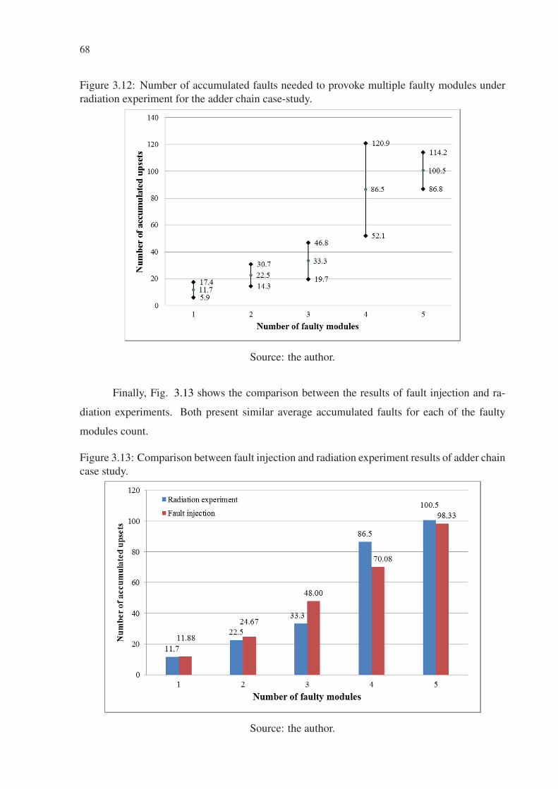
68
Figure 3.12: Number of accumulated faults needed to provoke multiple faulty modules underradiation experiment for the adder chain case-study.
Source: the author.
Finally, Fig. 3.13 shows the comparison between the results of fault injection and ra-
diation experiments. Both present similar average accumulated faults for each of the faulty
modules count.
Figure 3.13: Comparison between fault injection and radiation experiment results of adder chaincase study.
Source: the author.

69
3.3 Summary
A multiple fault injection platform to evaluate accumulated SEU effects in Virtex-5
FPGA is presented. The platform uses bit-flip positions generated by a pseudo random gen-
erator or taken from a database composed of pre-collected real bit-flips location detected from
previous neutron accelerated experiments at ISIS facilities. The flipped bits distribution of real
radiation test and fault injector were shown and analyzed. Also, the effects of accumulation
SEUs on a design using real radiation test and fault injection were tested. Results show the
capability of the proposed platform to predict the effects of radiation in FPGA designs and
mitigate the side-effects related to internal fault injectors.
In the next chapter, it is presented a survey of correction mechanisms for SRAM-based
FPGAs, and these solutions are analyzed taking into account the current and future context of
FPGAs.

70

71
4 MITIGATION TECHNIQUES TO CORRECT SOFT ERRORS IN SRAM-BASED FP-
GAS
Soft errors in the configuration memory bits of SRAM-based FPGAs have a persistent
effect, and they remain until the original configuration is restored. Hardened by design tech-
niques at the design level such as TMR (Triple Modular Redundancy) (BOLCHINI; MIELE;
SANTAMBROGIO, 2007), X-TMR (BRIDGFORD; CARMICHAEL; TSENG, 2008), partial
TMR (PRATT et al., 2006), are commonly used to increase the radiation tolerance by means of
fault masking. TMR masks the effects of soft errors by using majority voters and hardware trip-
lication (spatial redundancy) but does not correct the faults. Still, it is necessary to complement
these techniques with a correction mechanism to avoid fault accumulation in the configuration
memory. This approach effectively increases the mean time to failure (MTTF) as shown in
Ostler et al. (2009).
Memory scrubbing is a well-known correction technique for the configuration memory
of SRAM-based FPGAs. It consists on writing the configuration memory after the FPGA is
configured to restore its original content. It is often a transparent operation for the running
application. This capability is possible because modern FPGAs offer a dynamic partial recon-
figuration (DPR) feature. The circuit that enables the scrubbing is commonly named scrubber.
Additionally, readback is the process of reading the configuration memory of the FPGA after
it is configured. Both processes (readback and scrubbing) can be used to implement different
scrubbing methodologies as shown in Herrera-Alzu and Lopez-Vallejo (2013).
Any of the following scrubbing architectures or methodologies can correct SEU or MBU
in the configuration memory of the FPGA. It all depends on the resources used to protect the
configuration memory. For example, if the internal ECC (SECDED) of the configuration mem-
ory frames is used, the scrubber will only be able to correct one bit-flip and detect two bit-flips.
On the other hand, if an external golden reference of the configuration memory is used, the
scrubber will be able to correct any MBU size. Also, it is possible to use ad hoc ECC codes
protection schemes with scrubbing to correct SEU and MBU.
4.1 Scrubbing Architectures and Methodologies
Two primary criteria can classify scrubbers. The first is the architecture of the scrubbing
system and the second is the scrubbing methodology adopted. The scrubbing classification is

72
summarized in Fig. 4.1.
Figure 4.1: Proposed scrubber classification.
Scrubbers classification
Architecture Methodology
By the location By the Implementation method By the correction trigger event By the scrubbing granularity
Internal
External
Hardware
Software
Preventive scrubbing
Readback scrubbing
Error-driven scrubbing
Device oriented
Frame oriented
Module oriented
Task-driven scrubbing
Source: the author.
Regarding the architecture criteria, it is possible to classify scrubbers by the location and
the implementation method of the scrubber.
Scrubbing can be implemented using an internal or external configuration interface as
shown in Berg et al. (2008). When an external configuration interface is used, the scrubbing
logic is implemented outside the FPGA. The SelectMAP interface has the highest data through-
put. So, it can enable the fastest method to scrub the configuration memory. As an example,
the maximum frequency of the ICAP module in the Xilinx 7 Series Family of Xilinx is 100
MHz, and it has a 32-bit data interface. This configuration interface can achieve a maximum
data throughput of 400 Mbytes/s. The JTAG interface is also suitable to scrub the configuration
memory (VERA, 2009), however, depending on the application and the radiation environment,
it is not suitable for a scrubbing implementation. External scrubbers are presumed to be more
radiation tolerant than internal scrubbers since they can be implemented as a custom ASIC.
On the other hand, there is only one internal interface, the ICAP (XILINX, 2012b). An
internal scrubber needs to be implemented with the programmable blocks of the FPGA, so, it is
also vulnerable to soft errors. However, it is possible to apply hardening by design techniques
to internal scrubbers (HEINER; COLLINS; WIRTHLIN, 2008; LEGAT; BIASIZZO; NOVAK,
2012; EBRAHIM; ARSLAN; ITURBE, 2014). Using an internal scrubber, we avoid the power
consumption penalties of another device in the system. Fig. 4.2 represents the difference be-
tween internal and external scrubbers.
Also, scrubbers can be implemented in software or hardware. Hardware implementa-
tions use custom logic such as FSMs (Finite State Machines). This approach achieves faster
error detection and correction, but it lacks flexibility. The scrubbing process can be imple-

73
Figure 4.2: Internal vs. external scrubber.
Source: (HERRERA-ALZU; LOPEZ-VALLEJO, 2013).
mented in software using a microprocessor with the advantage of high flexibility to implement
different complex scrubbing methodologies but with lower configuration speeds and lower en-
ergy efficiency. For the highest energy efficiency, a hardware approach must be used. Fig.
4.3 shows a scrubber implemented in software. Few works in the literature use the software
approach; one example is the work of Vera (2009) that implements the scrubber in a custom
processor.
Figure 4.3: Software-based scrubber.
Source: (HERRERA-ALZU; LOPEZ-VALLEJO, 2013).
Regarding the methodology approach, it is possible to classify scrubbers by the event
that triggers the configuration memory correction and also by the granularity of the scrubbing.
The event that triggers the scrubbing process can classify scrubbers in four different
methodologies. The first is informally known as a blind scrubbing and also open loop scrubbing.
This method implements a preventive scrubbing and is the simplest methodology. It consists of a
periodic scrub of the configuration memory after a predefined scrub interval. The scrubbing rate
can be fixed or adaptive. On the other hand, readback scrubbing (or close loop scrubbing) refers

74
to do periodical readbacks until a soft error is detected; only then a scrub cycle is executed.
With a readback scrubbing methodology, it is possible to achieve lower energy consumption
since only when a soft error is detected, the scrubbing is enabled.
Fig. 4.4 shows the difference between preventive and readback scrubbing.
Figure 4.4: Examples of: (a) Preventive scrubbing (Blind). (b) Readback scrubbing.
Time
Scrubbing interval
Scrubbing time
Readback interval
Readback time
Time
Scrubbing time
(a)
(b)
Soft error
detected
Source: the author.
The soft error detection during readback can be implemented using Error Detection and
Correction Codes (EDAC) on the configuration frames or comparing the configuration data
with an external reference. This reference is usually a radiation-hardened external memory that
keeps a copy of the original configuration. A more detailed description of different schemes
using EDAC is presented in the next section.
The third methodology is the functional error-driven scrubbing. A scrub cycle is enabled
when the scrubber receives an error signal from the functional design. This method can be used
in TMR designs where the voter can detect a module with a functional error.
The last methodology is based on the task implemented in the FPGA. This method is
proposed in Santos et al. (2014), and it adapts the scrubbing time according to the criticality
of the task. The motivation is explained in Fig. 4.5. It is possible to observe that if the time
between the scrubbing execution and the task execution is long enough, there is the possibility
that an error affects the task before another scrubbing is executed (case I). Another case is when
there are wasted scrubbing executions because between executions the user design is idle (case
II). The last case (case III) is when the scrubbing is executed close to the task execution time
minimizing the probability of an error affect the task execution.

75
Figure 4.5: The relation of scrubbing execution and task execution.
I
2II
III
task execution scrubbing execution
W1 W2
t1 t2
W1 W2
SEU
W1 W2
time
time
time
wasted scrubbing execution
Fig. 1. Motivation example.Source: (SANTOS et al., 2014).
Finally, the scrubbing granularity can classify scrubbers in three groups. The first is
the device-oriented scrubbing, also known as full scrubbing. It treats the configuration mem-
ory as a whole. On the other hand, frame-oriented and module-oriented methodologies repairs
only selected zones. These methodologies are also known as partial scrubbing. Frame-oriented
scrubbing is the finest granularity possible, and a good knowledge of the configuration memory
is needed. Module oriented scrubbing can be implemented with the assistance of a dynamic par-
tial reconfiguration design flow and partial bitstreams. Fig 4.6 presents the differences between
module-oriented and device-oriented scrubbing.
The arrows indicate the repair direction of the configuration memory. This repair direc-
tion is standard for the Xilinx Virtex FPGA families.
Device-oriented scrubbing can be very costly in terms of energy consumption and time
to repair (scrubbing time) because the size of the bitstream is becoming very large each new
generation. Thus, to reduce the overhead of memory scrubbing, module-oriented scrubbing
must be applied.
Please note that memory scrubbing has some limitations. It cannot detect, nor correct
soft errors in user flip-flops or latches, nor in LUTs used as shift registers (SRL161) or as
distributed RAM (LUT-RAM). The user logic modifies the bits in these storage resources, so
1SLR16 are Xilinx primitive blocks to implement shift registers using LUTs.

76
Figure 4.6: Comparison of scrubbing methodologies with different granularities.
Start
End
Frame
row
1st
Frame
Final
Frame
(a) Device-oriented Scrubbing.
Module A Module B
(b) Module-oriented Scrubbing.
Source: the author.
the scrubber is not able to detect if a change in a bit is intended or not. In these cases, other
techniques as EDAC should be used. Also, it cannot correct soft errors in the internal circuitry
of the configuration controller (like Xilinx ICAP, JTAG or SelectMAP). In these cases, a power
cycle and full reconfiguration are needed to restore its functionality.
4.2 Ad hoc schemes using error detection and correction codes (EDAC)
Readback and scrubbing is one of the techniques mentioned before that have gained at-
tention by the scientific community in recent years. This technique is also the one that Xilinx
uses to mitigate soft errors in their FPGA devices. Combining EDAC with readback and scrub-
bing have been a good solution to mitigate soft errors in FPGAs until now. However, these
techniques will always have a tradeoff between overhead and detection or correction capability.
Xilinx offers two approaches to deal with soft errors in the configuration memory. The
first approach (CHAPMAN, 2010) is based on the inherent ECC bits (Hamming codes) stored
in each of the frames of the configuration memory and, also in the CRC value that protects
the whole configuration memory. This approach is the first solution from Xilinx to automate
the soft error mitigation in the configuration memory of the FPGA. It can be implemented in
Xilinx FPGAs with dynamic partial reconfiguration capability as the Virtex-4 and Virtex-5.
The scheme can only correct one bit-flip and detect two bit-flips per configuration frame, but
the correction is fast because the correction is done without accessing to an external memory

77
reference. During the bitstream generation, the ECC parity bits are calculated. In the case of
Virtex-5 FPGA, each frame has 12 ECC bits.
The solution is implemented using two Xilinx primitive blocks: the ICAP block and
the FRAME_ECC block. The ICAP block is the access port to the configuration memory, and
the FRAME_ECC is responsible for calculating the ECC parity bits when the frame is read
back. Then, it is possible to find bit-flips in the frame by a syndrome value. The syndrome is
generated from the ECC parity bits and the other data bits from the frame. Table 4.1 explains
how to interpret the syndrome value in Virtex-5 FPGAs.
Table 4.1: Syndrome value interpretation.
Syndrome Bit 11 Syndrome Bit [10:0] Error Statusbit 11 = 0 bits [10:0] = 0 No bit-flips.bit 11 = 1 bits [10:0] 6= 0 Single bit error, bits [10:0] denote indi-
rectly the bit-flip position.bit 11 = 1 bits [10:0] = 2n Single bit error in a parity bit,bit 11 = 0 bits [10:0] 6= 0 double-bit error, not correctable.
Source: (XILINX, 2012b).
The second approach is based on Xilinx proprietary IP core named Soft Error Mitigation
(SEM) (XILINX, 2012a). This core is targeted only for the newer FPGA families: Virtex-
6, Spartan-6 and 7 series, including the Xilinx SoC Zynq, which is composed by a dual-core
ARM processor and an FPGA. This scheme has three options for error correction. The first is
also based on the inherent ECC bits as shown in the first approach and has the same correction
capabilities. The second option is based on the combination of the ECC bits and the CRC
code of all the configuration bits. This option increments the correction capability, and now is
possible to correct up to two bit-flips (adjacent) per configuration frame. The third option is
based on the classic approach of a scrubber, using an external golden reference to repair bit-
flips in frames. With this option, the scrubber can correct any size of MBU in the configuration
memory. During the synthesis, place and route of this IP core, it is possible to determine which
are the essential bits of a design, so it is possible to discriminate if a bit-flip in the configuration
memory can affect the design or not (CRABILL; CHANG, 2014).
Due to increase of MBU events in modern devices, works in the literature (LANUZZA et
al., 2010; ARGYRIDES; PRADHAN; KOCAK, 2011; PARK; LEE; ROY, 2012; VENKATARA-
MAN et al., 2014a; VENKATARAMAN et al., 2014b) proposes solutions to correct MBUs us-
ing Hamming codes and parity codes without requiring access to a golden configuration mem-
ory reference. These works have low correction latency, and each work focuses on minimizing

78
the area overhead of the protection scheme.
For example Lanuzza et al. (2010) propose a solution where the configuration frame is
divided in data words, in order to obtain a virtual bit interleaving of the frame. A Hamming code
protects each data word as shown in Fig. 4.7. The effectiveness to correct MBU is dependent
on the number of data words used to divide the configuration frame. Also, the area overhead is
dependent on the number of data words selected.
Figure 4.7: Virtual interleaved data words to protect a configuration frame with Hammingcodes.
Configuration
Frame
B[0]
B[1]
B[2]
Hamming Parity Check codes
check code 1
B[3]
B[4]
B[5]
B[6]
B[7]
Hamming Parity
Check
Calculator
Hamming Parity
Check
Calculator
check code 2
check code k
Fig. 2. EDAC codes calculation. Source: (LANUZZA et al., 2010).
In addition, Argyrides, Pradhan and Kocak (2011) propose a combination of Hamming
codes and parity codes to protect the configuration memory. Park, Lee and Roy (2012) propose
to apply 2-D Hamming codes. Both works suggest to map each configuration frame in a 2-D
matrix. Then, it is possible to use single error correction codes (SEC) to rows and columns.
The main limitation is that the correction capability strongly depends on the MBU pattern as
shown in Fig. 4.8. The figure shows examples of 2-D Hamming codes, where D, ER, EC are
configuration bit, row parity bit and column parity bit respectively. The X represents a bit error.
Recently, Venkataraman et al. (2014a) proposed the same virtual bit-interleaved scheme
presented in Lanuzza et al. (2010). However, the main difference is that the Hamming codes
are embedded in the configuration frames reducing the area overhead as shown in Fig. 4.9.
f+ is the configuration frame where Xi are the bits that are not essential for the functional
design. This work takes the advantage that usually the functional design does not use more
than 50% of the configuration bits of a frame. Nevertheless, the work does not mention that

79
Figure 4.8: Examples of correctable and non-correctable MBU patterns with an 2-D HammingCode. In (A), it is shown a 2-D Hamming codes with a 7× 7 matrix of configuration bits. In(B), a correct execution of 2-D Hamming codes correction with two iterations. In (C), a correctexecution in 3 iterations. In (D), two cases with incorrect execution. In (E), an equivalent caseas (C).
Source: (PARK; LEE; ROY, 2012).
depending on the configuration frame, it is possible to create shortcuts in the functional design.
These shortcuts appear because some of the non-used configuration bits are the controllers of
the interconnections close to the functional interconnections of the design.
Figure 4.9: Examples of Hamming codes embedded in the configuration frame.
1 X1 0 X2 1 1 X3X4 0 X5 1 X6X7 1 X8
1 0 0 0 1 1 1 0 0 0 1 0 0 1 0
f+
after embedding
Source: (VENKATARAMAN et al., 2014a).
Also, the same author presents another approach in Venkataraman et al. (2014b) where
the 2-D Hamming approach is extended to 3-D. Fig. 4.10 shows a frame protected by the 3-D
Hamming scheme. Extending Hamming codes to 3-D allows a better correction capability, but
the error correction latency is incremented.
Another work (RAO et al., 2014) proposes a technique to correct MBUs using inter-
leaved 2-D parity to detect MBUs in configuration frames. The detection capability is also
dependent on the MBU pattern. The interleaved approach allows them to reduce the area over-
head without a significant loss of the detection capability compared to a full 2-D parity as shown
in Park, Lee and Roy (2012).
The correction mechanism is implemented using Erasure codes. An Erasure code is a
data recovery mechanism that transforms m blocks into m+ n blocks such that the original m
blocks can be recovered from an arbitrary set of m blocks among m+n coded blocks as shown

80
Figure 4.10: Examples of Hamming codes extended to 3-D. A frame bits matrix of nr rows andnc columns is shown. The number of row hamming bits is nr × hr. The number of column
hamming bits is nc×hc. And the number of diagonal hamming bits isnd
∑j=1
hd j, where hd j is the
number of hamming bits for each diagonal j.
Parity bits
Frame bits
Diagonal
Column
hr
hc
Row
hd
nr
nd
nc
Source: (VENKATARAMAN et al., 2014b).
Figure 4.11: The erasure code approach.
Encoding Decoding
m data blocks
n redundant blocks
m+n blocks
Source: (RAO et al., 2014).
in Fig. 4.11.
For the implementation of the technique, each block is a configuration frame + parity
bits. They need to group the configuration frame in clusters to reduce the time to correct a
frame and also to reduce the area overhead. The time to repair is reduced because to correct one
frame it is necessary to read all the frames (included the redundant frame). The area overhead is
reduced because, with several clusters, it is possible to add only one redundant frame per cluster
as shown in Fig. 4.12. It is important to mention that this is the first work that focuses the
correction in the whole frame and not in the particular bit(s) flipped. This feature is important

81
because according to the architecture of modern FPGAs, the smallest addressable unit in the
configuration memory is the configuration frame.
Figure 4.12: Implementation of erasure codes in the configuration memory of an FPGA.
m Data
Frames
One Redundant Block
For Each Cluster
Redundant Bit for
Configuration Bits
Redundant Bit
for Parity Bits
Clu
ste
r 1
Clu
ste
r 2
Clu
ste
r C
v
v
Configuration Bit
Parity Bit
Configuration
Frame
Vertical Parity Bits
Ho
rizo
nta
l
Pa
rity
Bit
s
(Area of Each Redundant
Block is Equal to One
Frame with I2D)
Source: (RAO et al., 2014).
The area overhead and the detection and correction time tradeoff are shown in Fig. 4.13.
The detection time is constant because it is only dependent on the parity bits in each frame. The
correction time is reduced when more clusters are used. With more clusters, fewer configuration
frames are needed to correct one error, but the memory (BRAM) overhead increases.

82
Figure 4.13: Error detection and correction time vs. memory overhead.
0
4
8
12
16
20
1 10 20 30 40 50 60 70 80 90 100 0
2
4
6
8
10
Tim
e [m
s]
# o
f R
equir
ed B
RA
M U
nit
s
Number of clusters
Required BRAM UnitsRecovery Time
Average Detection TimeWorst Case Detection Time
Source: (RAO et al., 2014).
4.3 Enabling MBU correction capability with TMR
An example of a work that takes advantage of the TMR masking technique to implement
the correction mechanism is shown in Herrera-Alzu and Lopez-Vallejo (2011). It is imple-
mented a self-reference scrubber, where the correction mechanism is based on the information
of three identical FPGAs (in device-level TMR) with identical bitstreams. Fig. 4.14 shows the
block diagram of the self-scrubber. This approach can correct any MBU pattern since it can re-
construct the configuration frame based on the information of the other two copies of the frame.
The scrubber needs to be implemented outside of the three FPGAs in order to maintain the same
bitstream in all the three FPGAs. The main drawbacks are the increased power consumption
and area overhead due to the triplication of the system at device-level.
Another work that benefits from the hardware redundancy to correct the bitstream is
shown in (UPEGUI; IZUI; CURCHOD, 2012). This work mentions a method to create repli-
cated partial bitstreams of modules in a TMR fashion as the proposed technique in this work.
The method is based on the dynamic partial reconfiguration design flow, using reconfigurable
partitions (RPs) and reconfigurable modules (RMs). This work describes all the steps to gener-
ate the bitstream triplication but it lacks of information related to the reliability of the technique
or any comparison of the performance of the technique with other works.

83
Figure 4.14: Block diagram of a self-reference scrubber.
Source: (HERRERA-ALZU; LOPEZ-VALLEJO, 2011).
4.4 Comparison of Correction Techniques
This chapter described most of the architectures and methodologies used to implement
scrubbing mechanisms. In this last section, a comparison between them is done, comparing
the main aspects of the scrubbing mechanism: area overhead, performance (error correction
latency), power consumption and reliability using the same classification proposed in Fig. 4.1.
For the architecture criteria, it is compared the area overhead, power consumption and reliabil-
ity. For the methodologies criteria, it is compared the performance (error correction latency)
and power consumption. Regarding the techniques that use ad hoc schemes using EDAC will
always have some overhead in terms of area because in these schemes it is needed some type of
redundancy (e.g. parity bits) to be stored in a memory device.
Table 4.2: Comparison of scrubber architectures due to the location of the scrubber.
Area Overhead Power Consumption ReliabilityInternal Low because is in-
cluded in the config-urable logic.
Lower compared to ex-ternal implementation.
More susceptible to softerrors because it is imple-mented in programmablelogic.
External High due to one extradevice to the system.
Higher due to extra de-vice in the system.
Better because it is presumedthat can be implemented in arad-hard device.
Source: the author.

84
Table 4.3: Comparison of scrubber architectures due to the implementation method.
Area Overhead Power Consumption ReliabilitySoftware High, it needs a proces-
sor and memory.Higher compared to thehardware approach.
Depends on the processor,and if is a hardcore or soft-core.
Hardware Low, it is implementedwith a FSM
Lower compared to thesoftware approach
Depends if is implemented ona rad-hard device or in pro-grammable logic.
Source: the author.
Table 4.4: Comparison of scrubber methodologies due to the correction trigger.
Error Correction Latency Power ConsumptionPreventive Depends on the scrub rate High compared to the other methodsReadback The lowest latency, Soft errors are
corrected as soon is detected.Lower than preventive scrubbing but thereadback rate imposes a penalty
Error-driven
Soft errors are only corrected whena functional error is detected.
Do not need a readback, the scrub rateis adapted to the error rate, reducing thepower consumption.
Task-driven
Soft errors are accumulated untilthe design needs to execute its task
Do not need a readback, the scrub rate isadapted to the task execution rate, reduc-ing the power consumption.
Source: the author.
Table 4.5: Comparison of scrubber methodologies due to the granularity.
Error Correction Latency Power ConsumptionDevice The highest compared with the other two. High compared to the other methodsFrame Only the frames with faults are scrubbed.
It requires knowledge of the configurationframes structure.
As with Module-oriented, offers lowerconsumption than device-oriented.
Module The scrubbing is focused on the zonewhere the user design relies.
As with Frame-oriented, offers lowerconsumption than device-oriented.
Source: the author.

85
5 PROPOSED MITIGATION TECHNIQUE
The proposed scrubbing technique (FLR-scrubbing) depends on a coarse grain TMR
design, where each TMR domain has the same frame data. So, each configuration frame of
the TMR design is triplicated in the FPGA. Therefore, any frame of the TMR design can be
repaired using the information of the other two identical frames. In this proposed technique,
coarse grain TMR is used to mask faults at the circuit level and also to enable the correction of
the faults in the configuration memory.
The description of the FLR-scrubbing technique is divided into two parts:
• In the first part, the process to generate the coarse grain TMR circuit with a customized
design flow is detailed. This process ensures that the configuration frames in each TMR
domain are the same.
• In the second part, a new scrubbing logic that uses the information of the triplicated
configuration frames to correct bit upsets is described.
Fig. 5.1 shows a block diagram of a coarse grain TMR design implemented using this
technique.
Figure 5.1: Block diagram of the frame redundancy scheme based on TMR design.
TMR
Domain 1
TMR
Domain 2
TMR
Domain 3
Fram
e 1
0
1
0
0
1
0
1
1
Fram
e 1
F
ram
e 1
0
1
0
0
1
0
1
1
0
1
0
0
1
0
1
1
. . .
. . .
. . .
Source: the author.

86
5.1 Customized Design Flow
The TMR design needs a particular placement to obtain the same configuration frames
for each TMR domain. Also, each TMR domain should be implemented in the FPGA with
same resources and routing. The placement of each TMR domain is obtained by placement
constraints, and it depends on the structure of the configuration memory of the target FPGA.
In Xilinx FPGAs, the configuration memory is structured as an array of configuration frames
vertically placed in the matrix. One frame fits into a single row, and each column may have
many vertical frames. For example in a Xilinx Virtex-5 FPGA, a CLB row and column has 36
frames each one with 1312 bits disposed vertically. Consequently, the height of a frame has
1312 bits, and each row has the height of a frame. TMR domains must be placed vertically
aligned, and covering an integer number of rows, as shown in Fig. 5.1.
This technique cannot be applied to the majority voter due to the limitations of tripli-
cating the majority voter with three identical placements of logic and inputs. So, there are two
possible solutions to correct upsets in the voters. The first one is to have a copy of the ma-
jority voter configuration frames in a memory and load this frames when needed to restore the
corrupted frames of the majority voter. The second solution is to place the voter outside the
FPGA. This option implies the use of another device as a rad-hard antifuse FPGA; however, it
may increase the system complexity and board area, but assuring the voter functionality under
radiation effects.
To obtain a coarse grain TMR design, where each TMR domain is synthesized, placed
and routed in the same manner, it is proposed a customized design flow as shown in Fig. 5.2.
This design flow is partially based on the Xilinx Standard design flow that uses the commercial
Xilinx tools to generate an FPGA bitstream from a hardware description of the design; and it
is also based on the RapidSmith tool (LAVIN et al., 2011), an academic tool to generate Hard
Macro Blocks (HMB) that assures that each TMR domain has the same configuration frames.
These HMB are used to implement each of the TMR domains because these blocks are
already placed and routed designs that can be instantiated in an FPGA design. The proposed
design flow begins with the generation of a placed and routed circuit from the original design
with the Xilinx standard design flow. Then, the RapidSmith tool receives the placed and routed
circuit in a Native Circuit Description (NCD) format and creates the HMB with a Native Macro
Circuit (NMC) format.
The second step is to create a new design project, which includes the three instances
of the HMB with the placement constraints. The voter of the coarse grain TMR design and

87
Figure 5.2: Customized design flow.
Original
design
Logic Synthesis & Place and Route
(PAR) with Xilinx Tools
Create a Hard Macro
Block from design RapidSmith Tool
Xilinx
Standard
Flow
*.vhd
*.ncd
*.nmc
Hard Macro block Hard Macro Block
(HMB)
Logic Synthesis & PAR of TMR + voter +
scrubber
Placement
constraints
Xilinx
Standard
Flow
TMR design with modified bitstream
(frame redundancy)
Voter Scrubber
*.vhd *.vhd *.nmc
*.ucf
(optional) (optional)
Source: the author.
the scrubber circuit can be optionally included in the project because they can be implemented
outside the FPGA. If the internal scrubber is selected, the ICAP block is used to access the
configuration memory. Otherwise, the SelectMAP port is used. Xilinx tools support the com-
bination of HDL designs with HMB to generate the final bitstream which has the same frame
data for the three TMR domains.
5.2 The Scrubbing Technique
The customized design flow ensures that the three TMR domains have the same config-
uration frames. The FLR-scrubbing technique uses this information to correct these regions.
The scrubber circuit needs to be configured with the location of the three TMR domains.
When the scrubber begins a scrub cycle, it reads the first frame of each TMR domain. Then, the
scrubber executes a bit level majority voting of the three frames and creates a fault-free (voted)
frame. In the best-case scenario, none of the frames needs to be corrected, so the scrubber
moves to the next frame position of each TMR domain. If any of the three frames is corrupted,

88
the scrubber replaces it with the fault-free (voted) frame.
In the worst-case scenario, three frames are corrupted due to the accumulation of bit
upsets. The scrubbing technique will be able to correct all the upsets if there is no more than
one upset per each relative bit position, as shown in Fig. 5.3. Please note that the frame from
the TMR domain 1 has an MBU, which would not be corrected by ECC (CHAPMAN, 2010),
but because our method votes bit by bit, the MBU of the frame from TMR domain 1 will be
voted out correctly.
Figure 5.3: Procedure to correct three identical frames with bit-level majority voting.
TMR
Domain 1
TMR
Domain 2
TMR
Domain 3
Fra
me
X
0
1
0
0
1
0
1
0
Fra
me
X
Fra
me
X
0
1
0
0
1
1
1
1
0
0
1
0
1
0
1
1
. . .
. . .
. . .
1
1
0
Bit-level
voting
11 0
0
1
0
0
1
0
1
1
0
1
0
0
1
0
1
1
0
1
0
0
1
0
1
1
11 1
Source: the author.
The correct execution of the scrubbing is based on the assumption that at most one of the
three bits voted is faulty. This scenario is expected because the three bits compared by the voter
are not physically adjacent, so it is very unlikely to have multiple bit upsets in two of the three
bits. We have not observed such cases under radiation to an accumulation up to 274 bit upsets
in average. However, if such unlikely case occurs, the scrubber will not detect nor correct the
frames and golden bitstream must be loaded from an external memory.

89
6 RESULTS ANALYSIS OF THE PROPOSED MITIGATION TECHNIQUE
6.1 Performance Results
We have validated our scrubbing technique into a Virtex-5 FPGA, part XC5VLX50T-
FFG1136. This device is manufactured with 65 nm technology, and it has a nominal core
voltage of 1.0V. It is worth noting that although, in this study we consider Xilinx FPGAs, the
proposed technique is generic and extendable to any SRAM-based FPGA that offers configura-
tion memory readback.
The scrubber was implemented in the FPGA, thus, it uses the ICAP block to access the
configuration memory. The ICAP block has a 32-bit data interface and can work at a maximum
clock frequency of 100 MHz.
6.1.1 Area Overhead
The area overhead of the FLR-scrubbing technique is low, and it corresponds to the area
of the scrubber circuit because it does not need any extra memory to store frame parity bits
or copies of the original frames. When comparing to techniques such as (RAO et al., 2014)
that need extra memory to store parity bits or (BERG et al., 2008; XILINX, 2012a) that needs
external memory to read the original (golden) configuration memory, our method can show a
good advantage. The area overhead of the FLR-scrubbing technique is also independent of the
size of the FPGA, and it is similar to Xilinx SEU Controller (CHAPMAN, 2010). The area
of Xilinx SEM IP (XILINX, 2012a) depends on the size of the FPGA and the selected error
correction method that can be based on the embedded ECC bits only, a combination of ECC
and CRC or the external golden memory. Related works compared in this paper (XILINX,
2012a; RAO et al., 2014; CHAPMAN, 2010) do not mention any mitigation technique for the
scrubber circuit. In our method, we propose to triplicate the scrubber to improve the reliability.
The presented area considers the triplication of the scrubber circuit. Table I presents our results
compared with previous works.
In our proposed method, it is not necessary to use an external memory to store the
original configuration memory as in the Xilinx solution (XILINX, 2012a) or a classic blind
scrubber. So the only area overhead comes from the scrubber circuit logic. Table 6.1 presents
our results compared with previous state-of-the-art related works.
The energy consumption overhead in our scheme is only limited to the consumption

90
Table 6.1: Area comparison results.
Scrubbing Scheme CLBs BRAMs External MemoryWork in (RAO et al., 2014)a 1100 (6 %) 4 (1 %) NoXilinx SEU Controller (CHAPMAN, 2010) 98 (3 %) 1 (2 %) NoXilinx SEM IP (XILINX, 2012a)b 108 (2 %) 3 (1 %) YesBlind Scrubbing (TMR) 341 (10 %) 12 (20 %) YesFLR-Scrubbing (TMR) 113 (3 %) 6 (10 %) No
aimplemented for a Virtex-6 VLX240T FPGA with 50 clusters and TMR redundancy. In this device, one framehas 2,592 bits.
bimplemented for an Artix-7 A100T FPGA without optional features. In this device, one frame has 3,232 bits.
Source: the author.
of the scrubber itself. For the Xilinx SEM IP (XILINX, 2012a) and the blind scrubbing, it
must take into account the power consumption of the external memory that stores the original
configuration memory. In the next sub-section is analyzed in detail the energy consumption.
6.1.2 Energy Consumption Overhead
We cannot neglect the power overhead imposed by the configuration memory scrubbing.
It is well known that the power consumption depends on the readback or scrub rate and the
scrub methodology adopted. So, to compare different scrubbing methodologies, we propose to
compare the energy consumed per configuration frame (Escrub− f rame). This parameter will give
us a better idea of the energy-efficiency of the technique and it is independent of the scrub rate
or the scrub methodology.
In the following it is explained the procedure to obtain the Escrub− f rame parameter. In
order to determine the energy consumption of our scrubbing technique, we measured the power
consumption (PFLR−scrubbing) and the scrub time (tscrub−time). With both parameters, it is possi-
ble to calculate the energy consumption as shown in equation 6.1:
EFLR−scrubbing = PFLR−scrubbing ∗ tscrub−time (6.1)
PFLR−scrubbing is composed of the static and dynamic power. In order to compare the
energy consumption of our technique with other scrubbing methodologies, the static power is
excluded. The main premise for this decision is that in the case of SRAM-based FPGAs, the
static power mainly depends on the size of the FPGA and is relatively constant during circuit
operation.

91
To perform the power measurements, it is used the INA219 current/voltage monitor chip
included on the Digilent Genesys FPGA board. The monitor chip is configured to return 16-
bit samples at 5 Hz, with each returned sample being the average of 128 sub-samples. The
measurement resolution of this monitor is 2 mA for the current and 4 mV for the voltage. One
monitor is placed on three different power sources: FPGA core, FPGA I/O and external flash
memory.
The average power consumption is calculated using equation 6.2:
PFLR−scrubbing = Pavg(n) =VCORE−RMS(n) ∗ ICORE−RMS(n) (6.2)
Where n is the number of samples, and VCORE−RMS(n), ICORE−RMS(n) are RMS values
of VCORE and ICORE respectively. The power consumption of the FPGA I/O interface and the
external flash memory are not considered since the FLR-scrubbing technique does not use any
interface with an external component. The RMS value is used to obtain the average power
because the current is not constant during the whole scrub cycle. As shown in equation 6.3, the
RMS value is defined as the quadratic mean of n samples.
IRMS(n) =
√I21 + I2
2 + · · ·+ I2n
n(6.3)
To obtain the dynamic power, first the static power is measured. For this, the FLR-
scrubber is implemented in the FPGA but with no clock stimuli. In a second step, the power
consumption is measured when the FLR-scrubber is set to run scrub cycles continuously. Sub-
tracting both power measurements, it is possible to obtain the dynamic power.
In order to measure the scrub cycle time, it is used an oscilloscope to measure the period
of a strobe signal that is toggled each time the scrubber finishes a scrub cycle. With the scrub
cycle time and the dynamic power, it is possible to obtain the energy consumption per scrub
cycle. So the last step is to divide by the number of frames protected during the scrub cycle as
shown in equation 6.4:
Escrub− f rame =EFLR−scrubbing
Framesscrub−cycle
(6.4)
The same procedure was followed to obtain the energy consumption of a blind scrubber
that uses as reference an external flash memory. We decided to choose the blind scrubber as a
reference point since it implements the simplest scrubbing methodology. In this case, we must
take into account the power consumption from the FPGA I/O interface and the external memory
as shown in equation 6.5:
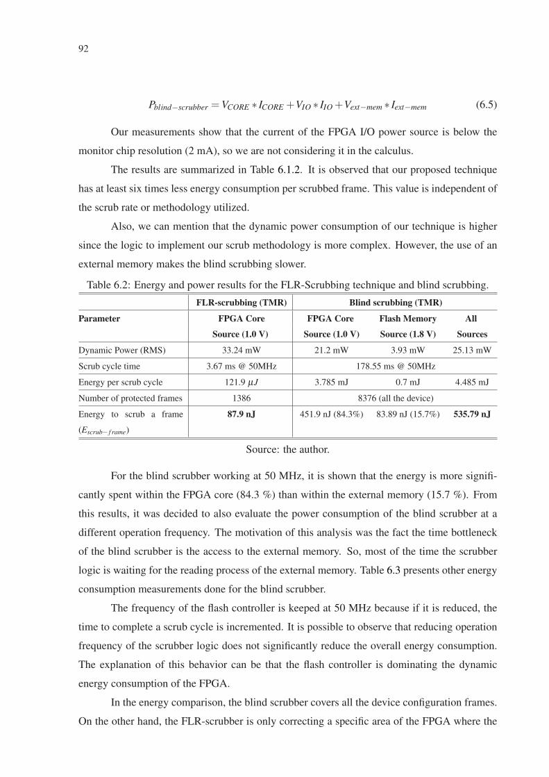
92
Pblind−scrubber =VCORE ∗ ICORE +VIO ∗ IIO +Vext−mem ∗ Iext−mem (6.5)
Our measurements show that the current of the FPGA I/O power source is below the
monitor chip resolution (2 mA), so we are not considering it in the calculus.
The results are summarized in Table 6.1.2. It is observed that our proposed technique
has at least six times less energy consumption per scrubbed frame. This value is independent of
the scrub rate or methodology utilized.
Also, we can mention that the dynamic power consumption of our technique is higher
since the logic to implement our scrub methodology is more complex. However, the use of an
external memory makes the blind scrubbing slower.
Table 6.2: Energy and power results for the FLR-Scrubbing technique and blind scrubbing.
FLR-scrubbing (TMR) Blind scrubbing (TMR)
Parameter FPGA Core FPGA Core Flash Memory All
Source (1.0 V) Source (1.0 V) Source (1.8 V) Sources
Dynamic Power (RMS) 33.24 mW 21.2 mW 3.93 mW 25.13 mW
Scrub cycle time 3.67 ms @ 50MHz 178.55 ms @ 50MHz
Energy per scrub cycle 121.9 µJ 3.785 mJ 0.7 mJ 4.485 mJ
Number of protected frames 1386 8376 (all the device)
Energy to scrub a frame
(Escrub− f rame)
87.9 nJ 451.9 nJ (84.3%) 83.89 nJ (15.7%) 535.79 nJ
Source: the author.
For the blind scrubber working at 50 MHz, it is shown that the energy is more signifi-
cantly spent within the FPGA core (84.3 %) than within the external memory (15.7 %). From
this results, it was decided to also evaluate the power consumption of the blind scrubber at a
different operation frequency. The motivation of this analysis was the fact the time bottleneck
of the blind scrubber is the access to the external memory. So, most of the time the scrubber
logic is waiting for the reading process of the external memory. Table 6.3 presents other energy
consumption measurements done for the blind scrubber.
The frequency of the flash controller is keeped at 50 MHz because if it is reduced, the
time to complete a scrub cycle is incremented. It is possible to observe that reducing operation
frequency of the scrubber logic does not significantly reduce the overall energy consumption.
The explanation of this behavior can be that the flash controller is dominating the dynamic
energy consumption of the FPGA.
In the energy comparison, the blind scrubber covers all the device configuration frames.
On the other hand, the FLR-scrubber is only correcting a specific area of the FPGA where the

93
Table 6.3: Total energy consumed per scrubbed frame for the blind scrubber at different opera-tion frequencies. From all supply sources (flash memory + FPGA core)
Blind scrubber version Escrub− f rame (nJ)Flash Controller @ 50 MHz,Scrubber logic @ 6.25 MHz
475.58
Flash Controller @ 50 MHz,Scrubber logic @ 50 MHz
535.79
Source: the author.
functional design is placed. It is impossible to cover the whole FPGA because the location of
the ICAP block and the internal scrubber logic prohibits the implementation of our customized
design flow explained in Section 5.1 This limitation can be solved by implementing the scrubber
externally to the FPGA as shown in Fig. 6.1.
Figure 6.1: Two options to implement the FLR-scrubber logic externally to the FPGA.
TMR Module 1
1000010101010101010
0101010101010101010
1000010101010101010
0101010101010101010
1000010101010101010
0101010101010101010
TMR Module 2
TMR Module 3
1000010101010101010
0101010101010101010
1000010101010101010
0101010101010101010
1000010101010101010
0101010101010101010
1000010101010101010
0101010101010101010
1000010101010101010
0101010101010101010
1000010101010101010
0101010101010101010
ASIC/FPGA
scrubber logic
SelectMAP interface
(a) Using an external ASIC or FPGA.
TMR Module 1
1000010101010101010
0101010101010101010
1000010101010101010
0101010101010101010
1000010101010101010
0101010101010101010
TMR Module 2
TMR Module 3
1000010101010101010
0101010101010101010
1000010101010101010
0101010101010101010
1000010101010101010
0101010101010101010
1000010101010101010
0101010101010101010
1000010101010101010
0101010101010101010
1000010101010101010
0101010101010101010
Zynq-7000 All Programmable SoC
ARM
Processor
(scrubber
logic)
(b) Using the Zynq-7000 All Programmable SoC.
Source: the author.
One option is to implement the FLR-scrubber logic in another ASIC/FPGA and using
an external interface to access the configuration memory as the SelectMAP interface. Another
option is to use a modern System on Chip (SoC) like the Xilinx Zynq-7000 All Programmable
SoC (XILINX, 2015b) to implement the FLR-scrubber logic in the ARM processor and access
the configuration frames through the dedicated interface.

94
6.1.3 Fault Detection and Repair Latency
The fault detection latency is the time needed to detect a soft error in the configuration
memory. This parameter depends on the number of configuration frames under analysis. The
upset repair latency is the time needed to correct a soft error in the configuration memory.
For the Xilinx SEM Controller (XILINX, 2012a), it must consider the read access time to the
external memory.
In the worst-case scenario, the upset detection latency is the time required to scan all the
analyzed configuration frames. This event can happen when an SEU/MBU occurs in a frame
after it has just been analyzed. The average upset detection latency is the half of the full scan
time. In Table 6.4, it is presented a comparison with other approaches taking into account
the time to scan one single frame (upset detection) and the time to correct one frame (upset
correction/repair). In the case of the Virtex-5, each frame has 1,312 bits.
Table 6.4: Comparison of the time to scan one frame and the time to repair one frame.
Scrubbing SchemeScan Time for Time to repair
Characteristicsone frame (µs) one frame (µs)
Work in (RAO et al., 2014)a 0.65 351 Uses BRAM to store parity frame
bits
Xilinx SEU Controller
(CHAPMAN, 2010)
0.82 240 The scrubber is based on a Pi-
coBlaze
Xilinx SEM IP (XILINX,
2012a)b
1.04 12 Uses an external memory (replace
method)
Blind Scrubbing (TMR) N/A 21 Uses an external memory
FLR-Scrubbing (TMR) 1.96 5 BRAM or external memory is not
needed
aimplemented for a Virtex-6 VLX240T FPGA with 50 clusters and TMR redundancy. In this device, one framehas 2,592 bits.
bimplemented for an Artix-7 A100T FPGA without optional features. In this device, one frame has 3,232 bits.
Source: the author.
One can observe that in our scheme, it is not necessary to scan all the configuration
frames of the FPGA, it only scans the configuration frames of the TMR design. In these frames
reside the highly potential bits that can generate a functional error in the circuit when flipped by
an energetic particle. In our case, the correction latency depends on the time to read the three
analyzed frames and the time to write the frame back into the configuration memory. For the
Xilinx SEM controller, the upset correction latency is strongly dependent on the access time to
the external memory. For the obtained result, we assume an external flash memory with a 16-bit

95
interface and a clock frequency of 50 MHz.
6.2 Neutron Radiation Results
The efficiency of the proposed scrubbing technique was evaluated with a Virtex-5 FPGA,
part XC5VLX50T-FFG1136. This FPGA has the capability of dynamic partial reconfiguration
through the ICAP interface. This interface is used to implement our scrubbing technique.
Experiments were performed in December 2014 at Los Alamos National Laboratory
(LANL), Los Alamos Neutron Science Center (LANSCE) Irradiation of Chips and Electron-
ics House II. The FPGA device was tested at normal incidence with an approximated neutron
flux of 1.43× 10⁶(n/cm2 × s). The neutron energy spectrum resembles the atmospheric one
between 1 and 750 MeV (VIOLANTE et al., 2007).
The board was placed in the radiation chamber and it was connected to a host computer
via two USB connections. The first one is used for the FPGA configuration and readback via
JTAG while the second one is used for the RS232-C communication with the scrubber.
The objective of the test is to analyze the efficiency of the proposed scrubbing method-
ology to correct multiple accumulated SEUs and MBUs. Therefore, the scrubber is protected
with TMR.
Fig. 6.2 shows the placement of the scrubber, and the three TMR domain zones that
the technique protects. The scrubber protects an area of 1,386 configuration frames, where the
TMR design is located. This area represents 720 CLBs (20 % of device CLBs) and 24 18K
BRAM blocks (20 % of device BRAM blocks). The protected area is relative small compared
to the FPGA total area because the ICAP position at the center of the FPGA, limits the area that
can be triplicated at the frame level. This inconvenience can be overcome implementing the
scrubber outside the FPGA and configure it with the SelectMAP interface.
The test procedure starts with the configuration of the FPGA, including the scrubber
circuit and the TMR protected zone. The FPGA is exposed to radiation and to the accumulation
of bit upsets in the configuration memory. The FLR-scrubbing technique is configured with
two pre-defined scrubbing rate during the test: one of 30 minutes and other one of 60 minutes.
During the accumulation period, periodic readbacks are performed with intervals of 5 minutes
to analyze the accumulation of upsets. So, once 30 minutes or 60 minutes are reached, the
FLR-scrubbing technique is activated to correct the TMR protected zone.
In order to save every scrubbing execution in a log file, when the scrubber finds bit upsets
in the TMR protected zone, it transmits to the host computer the frame address of corrupted

96
Figure 6.2: Placement of the TMR scrubber and the three TMR domain zones on a Virtex-5VLX50T.
1
TMR Domain 1
TMR Domain 2
TMR Domain 3
TMR
Scrubber
ICAP
Source: the author.
frames. The host PC executes a last readback to verify if TMR protected zone was correctly
scrubbed and if there is no remaining bit upsets. The host PC reconfigures the FPGA with the
original bitstream and a new run begins.
Experimental results are classified in four cases:
• Case 1: The scrubber sends a correct report to the host PC, and the readback files confirm
the proper operation of the scrubber.
• Case 2: The scrubber sends a wrong response to the host PC, and the readback files
confirm an error on the scrubber.
• Case 3: The scrubber sends a correct report to the host PC, but the readback files present
a wrong scrubbing correction.
• Case 4: The scrubber sends a wrong response to the host PC, but the readback data show
a correct scrubbing operation.
The percentage of occurrence of the four cases (1 to 4) is shown in Table 6.5. One can
see the average number of accumulated upsets per radiation test runs, the number of radiation

97
test runs and the percentage of occurrence of each one of the four cases described above.
Table 6.5: Classification and quantification of results after the scrubbing technique is applied.
avg. acc. upsets Total runs Case 1 Case 2 Case 3 Case 4
Scrub rate 1 (30 min) 145.7 33 87.8% 6.1% 6.1% 0%
Scrub rate 2 (60 min) 274 30 66.7% 26.7% 3.3% 3.3%
Source: the author.
Case 1 represents the correct behavior of the scrubber. In this case, the TMR in the
scrubber was adequate to mask any functional error, and the proposed technique was able to
correct all the accumulated bit-flips in the protected area. A graphical view of readback files
before and after the scrubbing is applied is shown in Fig. 6.3.
Figure 6.3: Graphical view of readbacks of a correct run (case 1). The spots are bit upsets inthe configuration memory.
(a) Readback just before the scrubber is activated. (b) Readback after the scrubber finished.
Source: the author.
Cases 2, 3 and 4 are wrong behaviors of the scrubber. Cases 2 and 4 are detectable errors
since the response of the scrubber shows some functional error. Fig. 6.4 shows a representative
example of a wrong behavior.
A detailed analysis of bit-flips in the readback files was done to diagnose if the origin of
functional error was in the scrubber circuit or the internal configuration controller of the FPGA
(ICAP). Since we have the information of the bit-flips occurred before each run execution, it was

98
Figure 6.4: Graphical view of readbacks of an incorrect run (cases 2 and 3).
(a) Readback just before the scrubber is activated. (b) Readback after the scrubber finished.
Source: the author.
developed an script to generate a faulty bitstream from the original bitstream with the accumu-
lated bit-flips of each run executed to compare the results obtained at the radiation experiment
and the results obtained by injecting the bit-flips in the original bitstream. If the results are the
same, the origin of the functional error relies on the scrubber circuit, but if not, there is the
possibility that the functional error was originated in the internal configuration controller of the
FPGA (ICAP).
After the analysis, it was found that 2 out of 63 runs have evidence of a possible error
in the internal configuration controller of the FPGA (ICAP). This means that, the majority
of functional errors observed during the radiation test were originated in the scrubber circuit
because the TMR scheme was defeated by the upset accumulation.
Case 3 is an undetectable error that was only observed after the analysis of the readback
files. The few cases analyzed show a behavior that the scrubber achieves the complete correction
of the protected zone but introduces bit-flips in other zones of the FPGA. This case is candidate
for a future analysis.
Case 3 is also the candidate case for finding an example where the scrubbing technique
is not able to correct or detect a fault when, as described in section 5.2, more than one bit of the
same relative bits position of the voted frames has an upset. However, after the analysis of the
readback files, it was not found any evidence of such scenario. All the runs, when the scrubber

99
failed to correct the configuration memory of the protected area, were due to a functional error
in the scrubber itself or because of a Single Event Functional Interrupt (SEFI) in the ICAP
block. So, this means that the error was in the scrubber and not in the technique itself.
Table 6.6 presents the cross section and Failures in Time (FIT) results of the scrubber
circuit considering the three cases of functional errors observed during the tests. As expected,
the reliability of the scrubber is reduced when more bit-flips are accumulated. The FIT is ob-
tained considering a flux of 13 neutrons/(cm2×h) (The New York City reference flux (JEDEC,
2006)). As a reference, it is also mentioned the estimated soft error rate of the Xilinx SEU Con-
troller (CHAPMAN, 2010). Please note that in this radiation test the focus is to demonstrate the
effectiveness of the FLR-scrubbing technique and not the reliability of the scrubber. Neverthe-
less, the scrubber reliability is critical for a real application.
Table 6.6: Cross section and Failure in Time at New York City.
Cross section (cm2) FITScrub rate 1 (30 min) 4.41×10⁻¹¹ 5.73Scrub rate 2 (60 min) 6.59×10⁻¹¹ 8.57Xilinx SEU Controller (CHAPMAN, 2010) N/A 8.6
Source: the author.
6.3 Fault Injection Results
The analysis of the results of the neutron radiation experiment showed that, in either
case, the FLR-scrubbing technique was defeated due to accumulated soft errors in the protected
area. Remembering that the only case where the technique is not able to detect or correct a fault
is when the same bit(s) position(s) of the same frames in each of the three regions have upset
bits within the same scrub cycle.
Therefore, the objective of the fault injection campaign is to determine the maximum
number of accumulated faults that the FLR-scrubbing mechanism can correct.
The fault injector is also implemented in the FPGA and shares the ICAP block with
the scrubber. The emulated upsets are a combination of random generated SEUs locations and
locations recorded from previously accelerated neutron radiation tests. The scrubber protects
the same area mentioned in the neutron radiation test (1,386 frames), and the fault injector is
constrained to inject faults in the same area protected by the scrubbing technique.
Fig. 6.5 shows the final placement of the scrubber, the fault injector and the three iden-

100
tical regions where the TMR design is located.
Figure 6.5: Placement of the scrubber, the fault injector and the three TMR domain zones on aVirtex-5 VLX50T.
TMR Domain 1
TMR Domain 2
TMR Domain 3
Scrubber
Fault Injector
ICAP
Source: the author.
The methodology to find the maximum number of accumulated SEUs was to inject faults
in steps of 10 faults per injection and then activated the scrubber to analyze if all the faults were
corrected. When faults remain in the protected area after executing the scrubbing mechanism,
the incrementation process of the number of accumulated SEUs is stopped. Then, the injector
starts to decrement the number of accumulated SEUs injected in steps of one fault to find the
final value. Finally, the fault injection campaign is ended. Figure 6.6 presents an example of a
fault injection campaign.
More than two hundred fault injection (FI) campaigns were performed, and more than
250,700 faults were injected. The results are summarized in Table 6.7. The maximum number
of accumulated bit upsets obtained in the fault injection campaign is ten times higher than the
bit upsets accumulated during the radiation test. These results can explain why in the neutron
radiation experiments it was not possible to find a case where the technique failed due to the
massive fault accumulation.
The results show that the technique can correct more than one thousand accumulated

101
Figure 6.6: Example of one fault injection campaign.
Time (s)
Accumulated
upsets
10
20
30
40
50
60
70
80
90
100
110
120
Scrubbing executed successfully
Scrubbing executed with errors
Source: the author.
Table 6.7: Fault Injection Results.
Maximum accumulated ValueSEUs correctedNumber of FI campaigns 212Average 1182.66Standard Deviation (σ ) 556.91Minimum 83maximum 2680
Source: the author.
faults on average in the protected area. This value represents a small percentage of the total
configuration bits in this area (less than 1 % in the tested area), but it represents a high accumu-
lation time of faults in a real environment.
In Fig. 6.7 is also show the fault injection results distribution and the probability distri-
bution fitness of a normal distribution using the kolgomorov-Smirnov test (NIST/SEMATECH,
2012) with the IBM SPSS software tool.
Fig. 6.8 shows the results issued from one fault injection campaign where after 224 ac-
cumulated faults the technique failed. In (a) is shown the readback of the configuration memory
before the technique is executed, and the result after the scrubbing mechanism is executed in
(b). In the figure, the matrix represents the configuration memory of the FPGA. Each cell of the
matrix represents a set of configuration bits related to a particular resource (e.g. CLB, BRAM,
etc.). In the case of Virtex-5 VLX50T, the matrix has 39 columns and 126 rows.

102
Figure 6.7: Histogram of the obtained results with fault injection and the Normal distributionfitness.
Source: the author.
Figure 6.8: Fault injection in the configuration memory. Red squares represent bit-flips in theconfiguration memory.
(a) 224 injected faults in the protected area (b) Only three faults remain after the scrub cycle.
Source: the author.

103
7 CONCLUSIONS AND INCOMING WORK
SRAM-based FPGAs are suitable for critical applications, but they are particularly sus-
ceptible to radiation-induced soft errors in the configuration memory. In this thesis, it was
analyzed the major dependability treats of SRAM-based FPGAs, focusing on SEEs. Also, it
was studied the factors that increases the susceptibility to soft errors such as voltage scaling and
aging. Then, it was presented the methods to analyze the reliability of systems implemented in
SRAM-based FPGAs with a particular interest in fault injection by emulation methods. Finally,
a novel scrubbing technique for the configuration memory of SRAM-based FPGAs is presented
and tested under radiation experiments and fault injection campaigns.
In the next sections, the main contributions of this thesis are summarized, then, the
future works are presented. Finally, the publications product of this thesis and the work did in
cooperation with other researchers are listed.
7.1 Main Contributions
7.1.1 Factors that increases the soft error rate in modern SRAM-based FPGAs
Radiation-induced soft errors in the configuration memory of SRAM-based FPGAs are a
major concern for critical applications implemented in these devices. The trend shows that this
scenario is getting worse. FPGA manufacturers as Xilinx achieved to reduce the susceptibility
of the SRAM cells that compose the configuration memory but due to the high densities of newer
devices, the soft error rate is continuously increasing. Based on neutron radiation experiment
results, we also observe the influence of aging and voltage scaling to the soft error rate in
SRAM-based FPGAs. Results have shown that the error rate can increase more than twice
when considering aging and voltage scaling. Also, it was found that aging effects have more
influence in the increment of the susceptibility than voltage scaling. So, it is important to
add this type of measurement and discussions when considering SRAM-based FPGAs for high
reliable applications.

104
7.1.2 Proposed Fault Injection Platform
It was presented a multiple fault injection platform to evaluate accumulated SEU effects
in the configuration memory of SRAM-based FPGAs. The platform uses bit-flip positions
generated by a pseudo-random generator or taken from a database composed of pre-collected
real bit-flips location detected from previous neutron accelerated experiments at ISIS facilities.
The location distribution of real radiation test and fault injector were shown and analyzed.
Also, the effects of accumulation SEUs on a design using real radiation test and fault injection
were tested. Results show the real capability of the platform proposed to predict the effects of
radiation in FPGA designs in a short time and mitigate the side-effects related to internal fault
injectors successfully.
7.1.3 Proposed Scrubbing Technique
It is presented a novel scrubbing mechanism that can effectively correct SEUs and MBUs
in the configuration memory of SRAM-based FPGAs. This technique offers good characteris-
tics in terms of area and energy overhead with low repair latency compared with other solutions.
The area overhead is independent of the selected device or area protected. The correction mech-
anism does not need an external memory, reducing effectively the system energy consumption
and the time to repair the fault. A comparison with a blind scrubber shows an energy reduction
of six times. It is important to mention that the correction effectiveness is not dependent on the
MBU pattern.
We have also presented an experimental evaluation of a novel scrubbing technique. Ra-
diation experiment results and fault injection campaigns have demonstrated the effectiveness of
the proposed method to correct multiple accumulated soft errors.
7.2 Future Work
7.2.1 Improving the proposed fault injection platform
In this thesis, it was proposed a fault injection platform that emulates soft errors in the
configuration memory using dynamic partial reconfiguration. The SEUs locations are taken
from previous radiation tests, and they are stored in a external flash memory. This architecture

105
achieves a high speed fault injection, but this characteristic is not always necessary. For ex-
ample, when it is required to predict the effects of an accelerated radiation test, the SEU rate
emulated is low compared with the maximum speed capacity.
A drawback of the current implementation is the flexibility of the fault injection plat-
form. When it is needed to adapt the fault injector to a particular application, it is required to
modify RTL codes, and also it is necessary to do some modifications to the assembly code that
runs in the PicoBlaze soft processor.
Therefore, an idea to improve the flexibility of the fault injection platform is to migrate
all the logic related to the fault injection process to the host PC. In the FPGA will only remain
the ICAP controller that is in charge of the low-level protocol required to access to the config-
uration memory. The rest will be controlled by the host computer. So, the SEU locations and
the time to inject the faults can be managed by the computer. The frame address and the bit
position to flip can be sent through a RS-232C communication. This will reduce the maximum
injection speed but can be tolerate by most of the practical cases we have used. To circuvent the
low speed interface communication, it is possible to implement the fault injector in the Zynq
SoC.
7.2.2 Evaluate the effectiveness of a TMR voter to trigger the scrubbing mechanism
In this work, it is presented the FLR-scrubbing technique with a fixed scrubbing rate.
The main idea is to analyze the reliability and power consumption when the voter of the TMR
protected circuit acts as the trigger of the scrubbing process. The voter will trigger the scrubbing
when one of the TMR domains presents a discrepancy with the other two. In this way, the
scrubbing rate dynamically adapts to the soft error rate. It will be possible to analyze if the FLR-
scrubbing technique can correct the accumulated faults after one of the TMR modules fails.
Another open question is if the TMR will mask the error the enough time until the scrubbing
finishes its execution.
7.2.3 Analyze the tradeoff between number of processed frames, time to repair and area
overhead with the FLR-Scrubbing technique
In the implemented version of the FLR-scrubbing presented in this work, the number
of frames processed in a single operation is three, one frame of each TMR domain. Since the

106
read and write operations to the configuration memory have fixed commands overhead (e.g. the
command overhead for reading one frame is the same as for 30 frames), it can be interesting to
analyze the benefits of processing more than three frames in the time to repair. As a penalty,
more area will be required to temporally store more frames than three.
7.2.4 Improving the reliability of the FLR-scrubber
To improve the reliability of the internal scrubber, the own FLR-scrubbing technique
can be applied to the scrubber. So, it will be triplicated with equal configuration frames for
each TMR domain. The scrubber will be capable of self-correct faults in its own configuration
frames and it will not need an external reference memory.
However, the ICAP should be also protected. The ICAP port is a critical part of the
scrubber since any error in the internal registers will provoke a wrong correction of the config-
uration memory. One possible solution is to test the ICAP before executing an scrubbing cycle.
The test will consist in reading and writing into an unused frame of the FPGA. The latest FPGA
families come with more than one ICAP module. To deal with errors in the ICAP, it will be
proposed a method to switch the selected ICAP in cases where the test of this block fails.
7.2.5 Improving the correction capability of the FLR-Scrubbing technique
One possible method to improve the correction capability of the FLR-Scrubbing tech-
nique is to use the information of the internal ECC of each frame to deduce if the bit-level voting
inside the scrubber is correct.
7.2.6 Improving the methodology to generate identical bitstream modules
The method to generate identical bitstream modules is based on Hard Macro blocks.
An academic tool was used to generate these blocks, but one limitation of theses blocks are
that commercial tools have unpredicted behaviors when using these blocks together with other
modules. Sometimes the bitstream generation process hangs at some point of the design flow
due to the use of these blocks. So, one possibility is to avoid using these blocks and create the
identical configuration frames using the XDL language (BECKHOFF; KOCH; TORRESEN,
2011). This language is a human-readable representation of the circuit and can be modified by

107
tools like the RapidSmith (LAVIN et al., 2011).
7.3 Publications related to this work
7.3.1 Journals
KASTENSMIDT, F.; TONFAT, J.; BOTH, T.; RECH, P.; WIRTH, G.; REIS, R.; BRU-
GUIER, F.; BENOIT, P.; TORRES, L.; FROST, C. Voltage scaling and aging effects on soft
error rate in SRAM-based FPGAs. In: MICROELECTRONICS RELIABILITY, Elsevier
Ltd, v. 54, n. 9-10, p. 2344-2348, sep. 2014.
TONFAT, J.; KASTENSMIDT, F.; RECH, P.; REIS, R.; QUINN, H. Analyzing the
Effectiveness of a Frame-level Redundancy Scrubbing Technique for SRAM-based FPGAs. In:
IEEE TRANSACTIONS ON NUCLEAR SCIENCE, v. 62, no. 6, pp. 3080-3087, dec. 2015.
7.3.2 Book chapter
TONFAT, J.; TARRILLO, J.; TAMBARA, L.; KASTENSMIDT, F.; REIS, R. Multiple
Fault Injection Platform for SRAM-based FPGA based on Ground-level Radiation Experiments.
In: KASTENSMIDT, F., RECH, P., FPGAS AND PARALLEL ARCHITECTURES FOR
AEROSPACE APPLICATIONS. 1st Ed. New York: Springer, 2016.
7.3.3 Conferences and workshops
TONFAT, J. ; KASTENSMIDT, F.; RECH, P.; REIS, R.; QUINN, H. Analyzing the Ef-
fectiveness of a Novel Frame-level Redundancy Scrubbing Technique for SRAM-based FPGAs.
In: NUCLEAR AND SPACE RADIATION EFFECTS CONFERENCE, NSREC 2015.
TONFAT, J.; KASTENSMIDT, F.; REIS, R. Energy Efficient Frame-level Redundancy
Scrubbing Technique for SRAM-based FPGAs. In: NASA/ESA CONFERENCE ON ADAP-
TIVE HARDWARE AND SYSTEMS, AHS 2015.
TONFAT, J.; RECH, P.; KASTENSMIDT, F.; REIS, R.; QUINN, H. A Novel Frame-
level Redundancy Scrubbing Technique for SRAM-based FPGAs. In: MILITARY AND

108
AEROSPACE PROGRAMMABLE LOGIC DEVICES WORKSHOP, MAPLD 2015.
TARRILLO, J.; TONFAT, J.; TAMBARA, L.; KASTENSMIDT, F.; REIS, R. Multiple
Fault Injection Platform for SRAM-Based FPGA Based on Ground-Level Radiation Experi-
ments. In: 16th IEEE LATIN AMERICAN TEST SYMPOSIUM, LATS 2015.
TONFAT, J.; KASTENSMIDT, F.; REIS, R. Frame-level Redundancy Correction Tech-
nique for SRAM-based FPGAs. In: FORUM FOR YOUNG PROFESSIONALS/MSc/PhD
STUDENTS, LASCAS 2015.
TONFAT, J.; AZAMBUJA, J.; NAZAR, G.; RECH, P.; FROST, C.; KASTENSMIDT,
F.; CARRO, L.; REIS, R.; BENFICA, J.; VARGAS, F.; BEZERRA, E. Measuring the Impact
of Voltage Scaling for Soft Errors in SRAM-based FPGAs From a Designer Perspective. In:
19th INTERNATIONAL MIXED-SIGNALS, SENSORS AND SYSTEMS TEST WORK-
SHOP, IMS3TW 2014. [S.l.: s.n.], p. 1-6, 2014.
KASTENSMIDT, F.; TONFAT, J.; BOTH, T.; RECH, P.; WIRTH, G.; REIS, R.; BRU-
GUIER, F.; BENOIT, P.; TORRES, L.; FROST, C. Aging and Voltage Scaling Impacts under
Neutron-induced Soft Error Rate in SRAM-based FPGAs. In: 19th IEEE EUROPEAN TEST
SYMPOSIUM, ETS 2014. [S.l.:s.n.], p. 1-2, 2014.
TAMBARA, L.; TONFAT, J.; REIS, R.; KASTENSMIDT, F.; PEREIRA, E.; VAZ, R.;
GONÇALEZ, O. Soft error rate in SRAM-based FPGAs under neutron-induced and TID ef-
fects. In: 15th IEEE LATIN AMERICAN TEST WORKSHOP, LATW 2014. v. 6, p. 1-6.
TONFAT, J.; AZAMBUJA, J.; NAZAR, G.; RECH, P.; FROST, C.; KASTENSMIDT,
F.; CARRO, L.; REIS, R.; BENFICA, J.; VARGAS, F.; BEZERRA, E. Analyzing the influ-
ence of voltage scaling for soft errors in SRAM-based FPGAs. In: 14th EUROPEAN CON-
FERENCE ON RADIATION AND ITS EFFECTS ON COMPONENTS AND SYSTEMS,
RADECS 2013. [S.l.: s.n.], p. 1-5, 2013.

109
7.4 Publications in cooperation with other researchers
CHIPANA, R.; KASTENSMIDT, F.; TONFAT, J.; REIS, R.; GUTHAUS, M. SET Sus-
ceptibility Analysis in Buffered Tree Clock Distribution Networks. In: 12th EUROPEAN
CONFERENCE ON RADIATION AND ITS EFFECTS ON COMPONENTS AND SYS-
TEMS, RADECS 2011. [S.l.: s.n.], p. 256-261, 2011.
TONFAT, J.; REIS, R. Low Power 3-2 and 4-2 Adder Compressors Implemented Using
ASTRAN. In: IEEE THIRD LATIN AMERICAN SYMPOSIUM ON CIRCUITS AND
SYSTEMS, LASCAS 2012. [S.l.: s.n.], p. 1-4, 2012.
CHIPANA, R.; KASTENSMIDT, F.; TONFAT, J.; REIS, R. SET Susceptibility Estima-
tion of Clock Tree Networks from Layout Extraction. In: 13th LATIN AMERICAN TEST
WORKSHOP, LATW 2012. [S.l.: s.n.], p. 1-6, 2012.
CHIPANA, R.; CHIELLE, E.; KASTENSMIDT, F.; TONFAT, J.; REIS, R. Soft-error
Probability due to SET in Clock Tree Networks. In: IEEE COMPUTER SOCIETY AN-
NUAL SYMPOSIUM ON VLSI, ISVLSI 2012. [S.l.: s.n.], p. 338-343, 2012.
TARRILLO, J.; TONFAT, J.; KASTENSMIDT, F.; REIS, R.; BRUGUIER, F.; BOUR-
REE, M.; BENOIT, P.; TORRES, L. Using Electromagnetic Emanations for Variability Charac-
terization in Flash-based FPGAs. In: IEEE Computer Society Annual Symposium on VLSI,
ISVLSI 2013. [S.l.: s.n.], p. 109-114, 2013.

110

111
REFERENCES
ALDERIGHI, M. et al. Using FLIPPER to Predict Irradiation Results for VIRTEX 2Devices. In: EUROPEAN CONFERENCE ON RADIATION AND ITS EFFECTS ONCOMPONENTS AND SYSTEMS, RADECS 2008. Jyvaskyla, Finland. Proceedings... Ny,USA: IEEE, 2008. p. 300–305. Available from internet: <http://ieeexplore.ieee.org/lpdocs/epic03/wrapper.htm?arnumber=5782731>. Accessed 04 May 2016.
ALEXANDRESCU, D.; STERPONE, L.; LOPEZ-ONGIL, C. Fault Injection and FaultTolerance Methodologies for Assessing Device Robustness and Mitigating Against IonizingRadiation. In: 19th IEEE EUROPEAN TEST SYMPOSIUM, ETS 2014. Paderborn,Germany. Proceedings... Ny, USA: IEEE, 2014. p. 1–6. Available from internet: <http://ieeexplore.ieee.org/lpdocs/epic03/wrapper.htm?arnumber=6847812>. Accessed 04 May 2016.
ALLEN, G.; SWIFT, G.; CARMICHAEL, C. Virtex-4QV Static SEU CharacterizationSummary. [S.l.], 2008. NASA Jet Propulsion Laboratory. Available from internet: <http://citeseerx.ist.psu.edu/viewdoc/download?doi=10.1.1.567.5414&rep=rep1&type=pdf>.Accessed 04 May 2016.
ARGYRIDES, C.; PRADHAN, D. K.; KOCAK, T. Matrix Codes for Reliable andCost Efficient Memory Chips. IEEE TRANSACTIONS ON VERY LARGE SCALEINTEGRATION (VLSI) SYSTEMS, [S.l.], v. 19, n. 3, p. 420–428, mar. 2011. Availablefrom internet: <http://ieeexplore.ieee.org/lpdocs/epic03/wrapper.htm?arnumber=5352255>.Accessed 04 May 2016.
AVIZIENIS, A. et al. Basic concepts and taxonomy of dependable and secure computing.IEEE TRANSACTIONS ON DEPENDABLE AND SECURE COMPUTING, [S.l.], v. 1,n. 1, p. 11–33, jan. 2004. Available from internet: <http://ieeexplore.ieee.org/lpdocs/epic03/wrapper.htm?arnumber=1335465>. Accessed 04 May 2016.
BAGATIN, M. et al. Factors Impacting the Temperature Dependence of Soft Errors inCommercial SRAMs. In: EUROPEAN CONFERENCE ON RADIATION AND ITSEFFECTS ON COMPONENTS AND SYSTEMS, RADECS 2008. Jyvaskyla, Finland.Proceedings... Ny, USA: IEEE, 2008. p. 100–106. Available from internet: <http://ieeexplore.ieee.org/xpl/articleDetails.jsp?arnumber=5782693>. Accessed 04 May 2016.
BAGATIN, M. et al. Impact of NBTI Aging on the Single-Event Upset of SRAM Cells.IEEE TRANSACTIONS ON NUCLEAR SCIENCE, [S.l.], v. 57, n. 6, p. 3245–3250,dec. 2010. Available from internet: <http://ieeexplore.ieee.org/lpdocs/epic03/wrapper.htm?arnumber=5658057>. Accessed 04 May 2016.
BARTH, J. L.; DYER, C. S.; STASSINOPOULOS, E. G. Space, Atmospheric, and TerrestrialRadiation Environments. IEEE TRANSACTIONS ON NUCLEAR SCIENCE, [S.l.], v. 50III, n. 3, p. 466–482, 2003.
BAUMANN, R. C. Radiation-induced soft errors in advanced semiconductor technologies.IEEE TRANSACTIONS ON DEVICE AND MATERIALS RELIABILITY, [S.l.], v. 5,n. 3, p. 305–315, 2005.
BECKHOFF, C.; KOCH, D.; TORRESEN, J. The Xilinx Design Language (XDL): Tutorialand use cases. In: 6th INTERNATIONAL WORKSHOP ON RECONFIGURABLE

112
COMMUNICATION-CENTRIC SYSTEMS-ON-CHIP, ReCoSoC 2011. Montpellier,France. Proceedings... Ny, USA: IEEE, 2011. p. 1–8. Available from internet: <http://ieeexplore.ieee.org/lpdocs/epic03/wrapper.htm?arnumber=5981545>. Accessed 04 May 2016.
BERG, M. et al. Effectiveness of Internal Versus External SEU Scrubbing Mitigation Strategiesin a Xilinx FPGA: Design, Test, and Analysis. IEEE TRANSACTIONS ON NUCLEARSCIENCE, [S.l.], v. 55, n. 4, p. 2259–2266, aug. 2008. Available from internet: <http://ieeexplore.ieee.org/lpdocs/epic03/wrapper.htm?arnumber=4636940>. Accessed 04 May 2016.
BOLCHINI, C.; MIELE, A.; SANTAMBROGIO, M. D. TMR and Partial DynamicReconfiguration to mitigate SEU faults in FPGAs. In: 22nd IEEE INTERNATIONALSYMPOSIUM ON DEFECT AND FAULT-TOLERANCE IN VLSI SYSTEMS, DFT2007. Rome, Italy. Proceedings... Ny, USA: IEEE, 2007. p. 87–95. Available from internet:<http://ieeexplore.ieee.org/lpdocs/epic03/wrapper.htm?arnumber=4358376>. Accessed 04May 2016.
BORKAR, S. Designing Reliable Systems from Unreliable Components: The Challengesof Transistor Variability and Degradation. IEEE MICRO, [S.l.], v. 25, n. 6, p. 10–16,nov. 2005. Available from internet: <http://ieeexplore.ieee.org/lpdocs/epic03/wrapper.htm?arnumber=1566551>. Accessed 04 May 2016.
BRIDGFORD, B.; CARMICHAEL, C.; TSENG, C. W. Single-Event Upset MitigationSelection Guide. [S.l.], 2008. Available from internet: <http://www.xilinx.com/support/documentation/application_notes/xapp987.pdf>. Accessed 09 Apr 2015.
CANNON, E. et al. The Impact of Aging Effects and Manufacturing Variation on SRAM Soft-Error Rate. IEEE TRANSACTIONS ON DEVICE AND MATERIALS RELIABILITY,[S.l.], v. 8, n. 1, p. 145–152, mar. 2008. Available from internet: <http://ieeexplore.ieee.org/lpdocs/epic03/wrapper.htm?arnumber=4385729>. Accessed 04 May 2016.
CERATTI, a. et al. On-chip aging sensor to monitor NBTI effect in nano-scale SRAM. In:IEEE 15th INTERNATIONAL SYMPOSIUM ON DESIGN AND DIAGNOSTICS OFELECTRONIC CIRCUITS & SYSTEMS, DDECS 2012. Tallinn, Estonia. Proceedings...Ny, USA: IEEE, 2012. p. 354–359. Available from internet: <http://ieeexplore.ieee.org/lpdocs/epic03/wrapper.htm?arnumber=6219087>. Accessed 04 May 2016.
CHANDRA, V.; AITKEN, R. Impact of technology and voltage scaling on the soft errorsusceptibility in nanoscale CMOS. In: IEEE INTERNATIONAL SYMPOSIUM ONDEFECT AND FAULT TOLERANCE IN VLSI SYSTEMS, DFT 2008. Boston, USA.Proceedings... Ny, USA: IEEE, 2008. p. 114–122. Available from internet: <http://ieeexplore.ieee.org/lpdocs/epic03/wrapper.htm?arnumber=4641164>. Accessed 04 May 2016.
CHAPMAN, K. SEU Strategies for Virtex-5 Devices. [S.l.], 2010. Available from internet:<http://www.xilinx.com/support/documentation/application_notes/xapp864.pdf>. Accessed 05Mar 2015.
CHOW, C. et al. Dynamic voltage scaling for commercial FPGAs. In: IEEE INTERNA-TIONAL CONFERENCE ON FIELD-PROGRAMMABLE TECHNOLOGY, FPT 2005.Singapore. Proceedings... Ny, USA: IEEE, 2005. p. 173–180. Available from internet: <http://ieeexplore.ieee.org/lpdocs/epic03/wrapper.htm?arnumber=1568543>. Accessed 04 May 2016.

113
CRABILL, E.; CHANG, P. Scan-Based Soft Error Mitigation of Configuration Memory inXilinx 7 Series FPGA Devices. In: WORKSHOP ON SILICON ERRORS IN LOGIC- SYSTEMS EFFECTS, SELSE 2014. [S.l.]. Proceedings... Ny, USA: IEEE, 2014.Available from internet: <http://selse.org/images/selse_2014/papers/selse_2014_13_paper.pdf>. Accessed 04 May 2016.
CRUISE, J. Statistics for Science Lecture Notes: Week 7. 2012. Available from internet:<http://www.macs.hw.ac.uk/~rc141/f78sc/notes07.pdf>. Accessed 04 May 2016.
CURD, D.; CRABILL, E. UltraScale Devices Maximize Design Integrity with Industry-Leading SEU Resilience and Mitigation. [S.l.], 2015. Available from internet: <http://www.xilinx.com/support/documentation/white_papers/wp462-ultrascale-SEU.pdf>. Accessed 14Jul 2015.
DODD, P.; MASSENGILL, L. Basic mechanisms and modeling of single-event upset in digitalmicroelectronics. IEEE TRANSACTIONS ON NUCLEAR SCIENCE, [S.l.], v. 50, n. 3,p. 583–602, jun. 2003. Available from internet: <http://ieeexplore.ieee.org/lpdocs/epic03/wrapper.htm?arnumber=1208578>. Accessed 04 May 2016.
DODD, P. E.; SEXTON, F. W. Critical charge concepts for CMOS SRAMs. IEEETRANSACTIONS ON NUCLEAR SCIENCE, [S.l.], v. 42, n. 6 pt 1, p. 1764–1771,1995. Available from internet: <http://ieeexplore.ieee.org/lpdocs/epic03/wrapper.htm?arnumber=488777>. Accessed 04 May 2016.
EBRAHIM, A.; ARSLAN, T.; ITURBE, X. On enhancing the reliability of internalconfiguration controllers in FPGAs. In: NASA/ESA CONFERENCE ON ADAPTIVEHARDWARE AND SYSTEMS, AHS 2014. Leicester, UK. Proceedings... Ny, USA: IEEE,2014. p. 83–88. Available from internet: <http://ieeexplore.ieee.org/lpdocs/epic03/wrapper.htm?arnumber=6880162>. Accessed 04 May 2016.
EDMONDS, L. D.; BARNES, C. E.; SCHEICK, L. Z. An Introduction to Space RadiationEffects on Microelectronics. Pasadena, California, USA, 2000. 83 p.
FACCIO, F.; CERVELLI, G. Radiation-induced edge effects in deep submicron CMOStransistors. IEEE TRANSACTIONS ON NUCLEAR SCIENCE, [S.l.], v. 52, n. 6, p.2413–2420, 2005.
GUZMAN-MIRANDA, H.; TOMBS, J. N.; AGUIRRE, M. A. FT-UNSHADES-uP: APlatform for the Analysis and Optimal Hardening of Embedded Systems in RadiationEnvironments. In: IEEE INTERNATIONAL SYMPOSIUM ON INDUSTRIALELECTRONICS, ISIE 2008. Cambridge, UK. Proceedings... Ny, USA: IEEE, 2008. p.2276–2281. Available from internet: <http://ieeexplore.ieee.org/lpdocs/epic03/wrapper.htm?arnumber=4677166>. Accessed 04 May 2016.
HEINER, J.; COLLINS, N.; WIRTHLIN, M. Fault Tolerant ICAP Controller for High-ReliableInternal Scrubbing. In: IEEE AEROSPACE CONFERENCE. Big Sky, MT. Proceedings...Ny, USA: IEEE, 2008. p. 1–10. Available from internet: <http://ieeexplore.ieee.org/lpdocs/epic03/wrapper.htm?arnumber=4526471>. Accessed 04 May 2016.
HERRERA-ALZU, I.; LOPEZ-VALLEJO, M. Self-reference scrubber for tmr systems basedon xilinx virtex fpgas. In: AYALA, J. et al. (Ed.). Integrated Circuit and System Design.Power and Timing Modeling, Optimization, and Simulation. [S.l.]: Springer Berlin

114
Heidelberg, 2011, (Lecture Notes in Computer Science, v. 6951). p. 133–142. Available frominternet: <http://dx.doi.org/10.1007/978-3-642-24154-3_14>. Accessed 04 May 2016.
HERRERA-ALZU, I.; LOPEZ-VALLEJO, M. Design Techniques for Xilinx Virtex FPGAConfiguration Memory Scrubbers. IEEE TRANSACTIONS ON NUCLEAR SCIENCE,[S.l.], v. 60, n. 1, p. 376–385, feb. 2013. Available from internet: <http://ieeexplore.ieee.org/lpdocs/epic03/wrapper.htm?arnumber=6412749>. Accessed 04 May 2016.
HUSSEIN, J.; SWIFT, G. Mitigating Single-Event Upsets. [S.l.], 2015. Available from inter-net: <http://www.xilinx.com/support/documentation/white_papers/wp395-Mitigating-SEUs.pdf>. Accessed 14 Jul 2015.
IBE, E. et al. Impact of Scaling on Neutron-Induced Soft Error in SRAMs From a 250 nm toa 22 nm Design Rule. IEEE TRANSACTIONS ON ELECTRON DEVICES, [S.l.], v. 57,n. 7, p. 1527–1538, jul. 2010. Available from internet: <http://ieeexplore.ieee.org/lpdocs/epic03/wrapper.htm?arnumber=5467170>. Accessed 04 May 2016.
JEDEC. JESD89A: Measurement and Reporting of Alpha Particle and Terrestrial CosmicRay-Induced Soft Errors in Semiconductor Devices. [S.l.], 2006.
KASTENSMIDT, F. et al. Voltage scaling and aging effects on soft error rate in SRAM-basedFPGAs. MICROELECTRONICS RELIABILITY, Elsevier Ltd, [S.l.], v. 54, n. 9-10, p.2344–2348, sep. 2014. Available from internet: <http://linkinghub.elsevier.com/retrieve/pii/S0026271414002960>. Accessed 04 May 2016.
KRETZSCHMAR, U. et al. Compact and Fast Fault Injection System for RobustnessMeasurements on SRAM-Based FPGAs. IEEE TRANSACTIONS ON INDUSTRIALELECTRONICS, [S.l.], v. 61, n. 5, p. 2493–2503, may 2014. Available from internet: <http://ieeexplore.ieee.org/lpdocs/epic03/wrapper.htm?arnumber=6560355>. Accessed 04 May 2016.
KUON, I.; ROSE, J. Measuring the Gap Between FPGAs and ASICs. IEEE TRANS-ACTIONS ON COMPUTER-AIDED DESIGN OF INTEGRATED CIRCUITS ANDSYSTEMS, [S.l.], v. 26, n. 2, p. 203–215, feb. 2007. Available from internet: <http://ieeexplore.ieee.org/lpdocs/epic03/wrapper.htm?arnumber=4068926>. Accessed 04 May 2016.
KUON, I.; TESSIER, R.; ROSE, J. FPGA Architecture: Survey and Challenges.FOUNDATIONS AND TRENDS® IN ELECTRONIC DESIGN AUTOMATION, [S.l.],v. 2, n. 2, p. 135–253, 2007.
LANGE, T. et al. Solar Orbiter Will Process Data Onboard Using Xilinx FPGAs. XCELLJOURNAL, n. 90, 2015.
LANUZZA, M. et al. A self-hosting configuration management system to mitigate the impact ofRadiation-Induced Multi-Bit Upsets in SRAM-based FPGAs. In: IEEE INTERNATIONALSYMPOSIUM ON INDUSTRIAL ELECTRONICS, 2010. Bari, Italy. Proceedings... Ny,USA: IEEE, 2010. p. 1989–1994. Available from internet: <http://ieeexplore.ieee.org/lpdocs/epic03/wrapper.htm?arnumber=5637493>. Accessed 04 May 2016.
LAVIN, C. et al. RapidSmith: Do-It-Yourself CAD Tools for Xilinx FPGAs. In: 21stINTERNATIONAL CONFERENCE ON FIELD PROGRAMMABLE LOGIC ANDAPPLICATIONS, FPL 2011. Chania, Greece. Proceedings... Ny, USA: IEEE, 2011. p.349–355. Available from internet: <http://ieeexplore.ieee.org/lpdocs/epic03/wrapper.htm?arnumber=6044842>. Accessed 04 May 2016.

115
LEGAT, U.; BIASIZZO, A.; NOVAK, F. SEU Recovery Mechanism for SRAM-Based FPGAs.IEEE TRANSACTIONS ON NUCLEAR SCIENCE, [S.l.], v. 59, n. 5, p. 2562–2571,oct. 2012. Available from internet: <http://ieeexplore.ieee.org/lpdocs/epic03/wrapper.htm?arnumber=6303851>. Accessed 04 May 2016.
LIN, C. Y. H. et al. Aging-aware statistical soft-error-rate analysis for nano-scaled CMOSdesigns. In: INTERNATIONAL SYMPOSIUM ON VLSI DESIGN, AUTOMATION,AND TEST, VLSI-DAT 2013. Hsinchu, Taiwan. Proceedings... Ny, USA: IEEE, 2013.p. 1–4. Available from internet: <http://ieeexplore.ieee.org/lpdocs/epic03/wrapper.htm?arnumber=6533854>. Accessed 04 May 2016.
MAITI, A.; MCDOUGALL, L.; SCHAUMONT, P. The impact of aging on an FPGA-basedPhysical Unclonable Function. In: 21st INTERNATIONAL CONFERENCE ON FIELDPROGRAMMABLE LOGIC AND APPLICATIONS, FPL 2011. Chania, Greece.Proceedings... Ny, USA: IEEE, 2011. p. 151–156.
NASEER, R. et al. Critical Charge Characterization for Soft Error Rate Modeling in 90nmSRAM. In: IEEE INTERNATIONAL SYMPOSIUM ON CIRCUITS AND SYSTEMS,ISCAS 2007. New Orleans, USA. Proceedings... Ny, USA: IEEE, 2007. p. 1879–1882.
NAZAR, G. L. Fine-Grained Error Detection Techniques for Fast Repair of FPGAs.125 p. Thesis (PhD) — UFRGS, 2013.
NAZAR, G. L.; CARRO, L. Fast Single-FPGA Fault Injection Platform. In: IEEEINTERNATIONAL SYMPOSIUM ON DEFECT AND FAULT TOLERANCE IN VLSIAND NANOTECHNOLOGY SYSTEMS, DFT 2012. Austin, USA. Proceedings... Ny,USA: IEEE, 2012. p. 152–157. Available from internet: <http://ieeexplore.ieee.org/lpdocs/epic03/wrapper.htm?arnumber=6378216>. Accessed 04 May 2016.
NAZAR, G. L.; SANTOS, L. P.; CARRO, L. Accelerated FPGA repair through shiftedscrubbing. In: 23rd INTERNATIONAL CONFERENCE ON FIELD PROGRAMMABLELOGIC AND APPLICATIONS, FPL 2013. Porto, Portugal. Proceedings... Ny, USA: IEEE,2013. p. 1–6. Available from internet: <http://ieeexplore.ieee.org/lpdocs/epic03/wrapper.htm?arnumber=6645533>. Accessed 04 May 2016.
NIST/SEMATECH. e-Handbook of Statistical Methods. 2012. Available from internet:<http://www.itl.nist.gov/div898/handbook/eda/section3/eda35g.htm>. Accessed 04 May 2016.
NUNEZ-YANEZ, J. L.; CHOULIARAS, V.; GAISLER, J. Dynamic Voltage Scaling ina FPGA-Based System-on-Chip. In: INTERNATIONAL CONFERENCE ON FIELDPROGRAMMABLE LOGIC AND APPLICATIONS, FPL 2007. Amsterdam, Netherlands.Proceedings... Ny, USA: IEEE, 2007. p. 459–462. Available from internet: <http://ieeexplore.ieee.org/lpdocs/epic03/wrapper.htm?arnumber=4380689>. Accessed 04 May 2016.
OSTLER, P. S. et al. SRAM FPGA Reliability Analysis for Harsh Radiation Environments.IEEE TRANSACTIONS ON NUCLEAR SCIENCE, [S.l.], v. 56, n. 6, p. 3519–3526,dec. 2009. Available from internet: <http://ieeexplore.ieee.org/lpdocs/epic03/wrapper.htm?arnumber=5341388>. Accessed 04 May 2016.
PARK, S. P.; LEE, D.; ROY, K. Soft-Error-Resilient FPGAs Using Built-In 2-D HammingProduct Code. IEEE TRANSACTIONS ON VERY LARGE SCALE INTEGRATION

116
(VLSI) SYSTEMS, [S.l.], v. 20, n. 2, p. 248–256, feb. 2012. Available from internet: <http://ieeexplore.ieee.org/lpdocs/epic03/wrapper.htm?arnumber=5682391>. Accessed 04 May 2016.
PRATT, B. et al. Improving FPGA Design Robustness with Partial TMR. In: IEEEINTERNATIONAL RELIABILITY PHYSICS SYMPOSIUM PROCEEDINGS,RELPHY 2006. San Jose, USA. Proceedings... Ny, USA: IEEE, 2006. p. 226–232. Availablefrom internet: <http://ieeexplore.ieee.org/lpdocs/epic03/wrapper.htm?arnumber=4017162>.Accessed 04 May 2016.
QUINN, H. et al. Radiation-induced multi-bit upsets in SRAM-based FPGAs. IEEETRANSACTIONS ON NUCLEAR SCIENCE, [S.l.], v. 52, n. 6, p. 2455–2461, dec.2005. Available from internet: <http://ieeexplore.ieee.org/lpdocs/epic03/wrapper.htm?arnumber=1589223>. Accessed 04 May 2016.
QUINN, H. et al. Domain Crossing Errors: Limitations on Single Device Triple-ModularRedundancy Circuits in Xilinx FPGAs. IEEE TRANSACTIONS ON NUCLEAR SCIENCE,[S.l.], v. 54, n. 6, p. 2037–2043, dec. 2007. Available from internet: <http://ieeexplore.ieee.org/lpdocs/epic03/wrapper.htm?arnumber=4395073>. Accessed 04 May 2016.
RAO, P. M. B. et al. Protecting SRAM-based FPGAs Against Multiple Bit Upsets UsingErasure Codes. In: 51st ANNUAL DESIGN AUTOMATION CONFERENCE ON DESIGNAUTOMATION, DAC 2014. New York, USA. Proceedings... New York, USA: ACMPress, 2014. p. 1–6. Available from internet: <http://dl.acm.org/citation.cfm?doid=2593069.2593191>. Accessed 04 May 2016.
REORDA, M. S.; STERPONE, L.; VIOLANTE, M. Efficient estimation of SEU effectsin SRAM-based FPGAs. In: 11th IEEE INTERNATIONAL ON-LINE TESTINGSYMPOSIUM. [S.l.]. Proceedings... Ny, USA: IEEE, 2005. p. 54–59. Available frominternet: <http://ieeexplore.ieee.org/lpdocs/epic03/wrapper.htm?arnumber=1498129>.Accessed 04 May 2016.
SANTOS, R. et al. Criticality-aware scrubbing mechanism for SRAM-based FPGAs. In:24th INTERNATIONAL CONFERENCE ON FIELD PROGRAMMABLE LOGICAND APPLICATIONS, FPL 2014. Munich, Germany. Proceedings... Ny, USA: IEEE,2014. p. 1–8. Available from internet: <http://ieeexplore.ieee.org/lpdocs/epic03/wrapper.htm?arnumber=6927476>. Accessed 04 May 2016.
SHOOMAN, M. Reliability of Computer Systems and Networks: Fault Tolerance,Analysis, and Design. [S.l.]: Wiley, 2002. (A Wiley-interscience publication).
STERPONE, L.; VIOLANTE, M.; REZGUI, S. An Analysis Based on Fault Injection ofHardening Techniques for SRAM-Based FPGAs. IEEE TRANSACTIONS ON NUCLEARSCIENCE, [S.l.], v. 53, n. 4, p. 2054–2059, aug. 2006. Available from internet: <http://ieeexplore.ieee.org/lpdocs/epic03/wrapper.htm?arnumber=1684058>. Accessed 04 May 2016.
TAMBARA, L. A. et al. Soft error rate in SRAM-based FPGAs under neutron-induced andTID effects. In: 15th LATIN AMERICAN TEST WORKSHOP, LATW 2014. Fortaleza,Brazil. Proceedings... Ny, USA: IEEE, 2014. v. 6, p. 1–6. Available from internet: <http://ieeexplore.ieee.org/lpdocs/epic03/wrapper.htm?arnumber=6841920>. Accessed 04 May 2016.
TARRILLO, J. Exploring the Use of Multiple Modular Redundancies for MaskingAccumulated Faults in SRAM-based FPGAs. 112 p. Thesis (PhD) — UFRGS, 2014.

117
TARRILLO, J. et al. Dynamic Partial Reconfiguration Manager. In: 5th Ny, USA: IEEELATIN AMERICAN SYMPOSIUM ON CIRCUITS AND SYSTEMS, LASCAS 2014.Santiago, Chile. Proceedings... Ny, USA: IEEE, 2014. p. 1–4. Available from internet: <http://ieeexplore.ieee.org/lpdocs/epic03/wrapper.htm?arnumber=6820293>. Accessed 04 May 2016.
TARRILLO, J. et al. Neutron Cross-Section of N-Modular Redundancy Technique inSRAM-Based FPGAs. IEEE TRANSACTIONS ON NUCLEAR SCIENCE, [S.l.], v. 61,n. 4, p. 1558–1566, aug. 2014b. Available from internet: <http://ieeexplore.ieee.org/lpdocs/epic03/wrapper.htm?arnumber=6870672>. Accessed 04 May 2016.
TONFAT, J. et al. Measuring the impact of voltage scaling for soft errors in SRAM-basedFPGAs from a designer perspective. In: 19th INTERNATIONAL MIXED-SIGNALS,SENSORS AND SYSTEMS TEST WORKSHOP, IMS3TW 2014. Porto Alegre, Brazil.Proceedings... Ny, USA: IEEE, 2014. p. 1–6.
UPEGUI, A.; IZUI, J.; CURCHOD, G. Fault Mitigation by Means of Dynamic PartialReconfiguration of Virtex-5 FPGAs. In: INTERNATIONAL CONFERENCE ONRECONFIGURABLE COMPUTING AND FPGAS, ReConFig 2012. Cancun, Mexico.Proceedings... Ny, USA: IEEE, 2012. p. 1–6. Available from internet: <http://ieeexplore.ieee.org/lpdocs/epic03/wrapper.htm?arnumber=6416752>. Accessed 04 May 2016.
VENKATARAMAN, S. et al. A bit-interleaved embedded hamming scheme to correctsingle-bit and multi-bit upsets for SRAM-based FPGAs. In: 24th INTERNATIONALCONFERENCE ON FIELD PROGRAMMABLE LOGIC AND APPLICATIONS,FPL 2014. Munich, Germany. Proceedings... Ny, USA: IEEE, 2014. p. 1–4. Availablefrom internet: <http://ieeexplore.ieee.org/lpdocs/epic03/wrapper.htm?arnumber=6927385>.Accessed 04 May 2016.
VENKATARAMAN, S. et al. Multi-directional error correction schemes for SRAM-basedFPGAs. In: 24th INTERNATIONAL CONFERENCE ON FIELD PROGRAMMABLELOGIC AND APPLICATIONS, FPL 2014. Munich, Germany. Proceedings... Ny, USA:IEEE, 2014. p. 1–8. Available from internet: <http://ieeexplore.ieee.org/lpdocs/epic03/wrapper.htm?arnumber=6927448>. Accessed 04 May 2016.
VERA, A. A programmable configuration scrubber for FPGAs. In: MILITARY ANDAEROSPACE PROGRAMMABLE LOGIC DEVICES, MAPLD 2009. [S.l.]. [s.n.], 2009.
VIOLANTE, M. et al. A New Hardware/Software Platform and a New 1/E Neutron Sourcefor Soft Error Studies: Testing FPGAs at the ISIS Facility. IEEE TRANSACTIONS ONNUCLEAR SCIENCE, [S.l.], v. 54, n. 4, p. 1184–1189, aug. 2007. Available from internet:<http://ieeexplore.ieee.org/lpdocs/epic03/wrapper.htm?arnumber=4291800>. Accessed 04May 2016.
WEISSTEIN, E. Radiation Definition. 2007. Available from internet: <http://scienceworld.wolfram.com/physics/Radiation.html>. Accessed 21 May 2015.
WHITE, D. Considerations Surrounding Single Event Effects in FPGAs, ASICs,and Processors. [S.l.], 2012. Available from internet: <http://www.xilinx.com/support/documentation/white_papers/wp402_SEE_Considerations.pdf>. Accessed 14 Jul 2015.

118
WIRTHLIN, M. J.; TAKAI, H.; HARDING, A. Soft error rate estimations of the Kintex-7FPGA within the ATLAS Liquid Argon (LAr) Calorimeter. JOURNAL OF INSTRUMENTA-TION, [S.l.], v. 9, n. 01, p. C01025–C01025, jan. 2014. Available from internet: <http://stacks.iop.org/1748-0221/9/i=01/a=C01025?key=crossref.77ef575bfef2b0871987484ea5aa005d>.Accessed 04 May 2016.
XILINX. LogiCORE IP Soft Error Mitigation Controller v3.4 Product Guide. [S.l.], 2012.Available from internet: <http://www.xilinx.com/support/documentation/ip_documentation/sem/v3_4/pg036_sem.pdf>. Accessed 29 Mar 2015.
XILINX. Virtex-5 FPGA Configuration User Guide. [S.l.], 2012. Available from internet:<http://www.xilinx.com/support/documentation/user_guides/ug191.pdf>. Accessed 05 Mar2015.
XILINX. 7 series FPGAs Configurable Logic Block User Guide. [S.l.], 2014. Available frominternet: <http://www.xilinx.com/support/documentation/user_guides/ug474.pdf>. Accessed13 Apr 2015.
XILINX. Radiation-Hardened, Space-Grade Virtex-5QV Family Overview. [S.l.], 2014.Available from internet: <http://www.xilinx.com/support/documentation/data_sheets/ds192_V5QV_Device_Overview.pdf>. Accessed 16 Jul 2015.
XILINX. Spartan-6 FPGA Configuration User Guide. [S.l.], 2014. Available from internet:<http://www.xilinx.com/support/documentation/user_guides/ug380.pdf>. Accessed 16 Apr.2015.
XILINX. Device Reliability Report. [S.l.], 2015. Available from internet: <http://www.xilinx.com/support/documentation/user_guides/ug116.pdf>. Accessed 16 Apr. 2015.
XILINX. Zynq-7000 All Programmable SoC Overview. [S.l.], 2015. Available from internet:<http://www.xilinx.com/support/documentation/data_sheets/ds190-Zynq-7000-Overview.pdf>. Accessed 15 Jul 2015.
YANG, E. et al. HHC: Hierarchical hardware checkpointing to accelerate fault recoveryfor SRAM-based FPGAs. In: 19th IEEE INTERNATIONAL ON-LINE TESTINGSYMPOSIUM, IOLTS 2013. Chania, Greece. Proceedings... Ny, USA: IEEE, 2013. p.193–198. Available from internet: <http://ieeexplore.ieee.org/lpdocs/epic03/wrapper.htm?arnumber=6604078>. Accessed 04 May 2016.

119
APPENDIX A
TÉCNICA DE CORREÇÃO DE ERROS PARA FPGAS BASEADOS EM SRAM
USANDO REDUNDANCIA A NIVEL DE FRAME
(PORTUGUESE EXTENDED ABSTRACT)
A.1 Introdução
Confiabilidade é um parâmetro de projeto importante para aplicações criticas tanto na
Terra como também no espaço. Os FPGAs baseados em memoria SRAM (doravante refer-
enciados como FPGAs) são atrativos para implementar aplicações criticas devido a seu alto
desempenho e flexibilidade (LANGE et al., 2015). No entanto, estes FPGAs são muito sus-
ceptíveis aos efeitos da radiação tais como os soft errors na memoria de configuração. Além
disso, outros efeitos como o envelhecimento (aging) ou escalonamento da tensão de alimen-
tação (voltage scaling) incrementam a sensibilidade à radiação dos FPGAs. (KASTENSMIDT
et al., 2014).
Existem FPGAs fabricados para serem tolerantes aos efeitos da radiação (XILINX,
2014b), mas eles são mais custosos, com menor desempenho e de difícil acesso de compra
comparados com seus pares comerciais conhecidos como COTS (Commercially-of-the-shelf )
FPGAs.
COTS FPGAs são dispositivos CMOS tradicionais com uma característica única. Eles
podem ser reconfigurados em campo. Isto significa que a sua função pode ser reprogramada de-
pois de ter sido fabricado. Esta capacidade de reconfiguração é possível devido a que os FPGAs
utilizam uma memoria de configuração baseada em células SRAM. Contudo, esta memoria de
configuração é a responsável da maioria de problemas de confiabilidade em FPGAs. Os FPGAs
são altamente susceptíveis a radiação ionizante devido a grande quantidade de células SRAM
na memoria de configuração.
Os efeitos em circuitos integrados devido à radiação ionizante podem ser classificados
como Single Event Effects (SEEs) ou Total Ionization Dose (TID). Para os FPGAs baseados em
SRAM, os SEEs são de mais preocupação.
Partículas altamente energizadas podem interatuar com o silício dos circuitos integrados
e podem provocar pulsos transientes nos nós dos transistores das células SRAM. Estes pul-
sos transientes podem ocasionar inversões nos bits (bit-flips) das células SRAM. Uma mesma
partícula pode inverter um ou mais de um bit na memoria de configuração de um FPGA. Quando

120
a partícula inverte um bit só, o evento é chamado de Single Event Upset (SEU), mas quando são
invertidas mais de uma célula de memoria o evento é chamado Multiple Bit Upset (MBU) ou
Multiple Cell Upset (MCU) dependendo da estrutura logica das células de memoria. Inversões
múltiplas de bits são cada vez mais comuns em nós tecnológicos modernos devido a peque-
nas dimensões dos transistores e a baixas tensões de operação (CHANDRA; AITKEN, 2008).
Como resultado, eventos com múltiplas inversões de bits estão aumentando em FPGAs moder-
nos (QUINN et al., 2007; WIRTHLIN; TAKAI; HARDING, 2014).
Então para poder implementar sistemas críticos em FPGAs, técnicas eficientes de mit-
igação de falhas devem ser usadas. Técnicas de tolerância a falhas são utilizadas para evitar
falhas nos sistemas. Redundância modular tripla ou TMR é a técnica de tolerância a falhas mais
comum de redundância espacial. Mas, a diferença dos ASICs onde os SEEs são usualmente
transientes, SEEs na memoria de configuração de um FPGA têm um efeito persistente. O efeito
persistente da falha significa que ela permanecerá ate alguma ação de correção for executada.
Então em FPGAs, TMR deve ser utilizado em conjunto com um mecanismo de correção da
memoria de configuração para evitar a acumulação de falhas. Ciclos de energia (power cycles)
ou reconfigurações completas do FPGA são mecanismos de correção conhecidos. No entanto,
estas técnicas implicam que o sistema não estará o 100% do tempo disponível para executar sua
função. Dependendo da aplicação, esta situação não é tolerável.
Memory scrubbing é outra técnica de correção de falhas para a memoria de configuração
do FPGA. Esta técnica pode corrigir a memoria de configuração sem ter que parar a execução
do sistema. Porém, com o aumento da taxa de falhas em FPGAs modernos, a taxa de scrubbing
também esta aumentando. Este fato impacta diretamente no consumo de potencia do sistema
(HERRERA-ALZU; LOPEZ-VALLEJO, 2013).
A técnica de scrubbing pode corrigir a memoria usando códigos de detecção e correção
de erros (EDAC) ou usando uma memoria de referencia golden que garante conter a infor-
mação original da memoria de configuração. Quando a abordagem EDAC é utilizada, existe
um balanço inerente entre a capacidade correção, a complexidade do scrubber1 e os custos em
área ou potencia. E no cenário atual, onde os eventos de falhas múltiplas estão aumentando, a
complexidade do scrubber e os custos de área e potencia estão aumentando também.
Por outro lado, se uma memoria de referencia golden é utilizada, o problema principal
é o tempo gasto para reparar as falhas. Existe um gargalo no acesso aos dados armazenados
numa memoria externa. A típica largura de banda de uma memoria externa é de 33 Mbps,
enquanto a largura de banda do acesso a memoria de configuração do FPGA pode chegar ate
1Um scrubber é o circuito encarregado de executar o processo de scrubbing.

121
3.2 Gbps (YANG et al., 2013). Existe uma brecha de mais de 100 vezes entre a largura de
banda de ambas as memorias. Além, o consumo de energia da memoria externa deve ser levado
em conta. Então, baixa largura de banda combinada com consumo extra de energia são os
problemas principais num cenário onde o tamanho da memoria de configuração dos FPGAs
modernos esta aumentando de maneira exponencial como mostrada na Figura A.1.
Figure A.1: Tamanho da memoria de configuração nos FPGAs maiores de cada uma dasfamílias Virtex da Xilinx.
'
/
/*
//
*
*
) 5&
# (
Fonte: DOCUMENTAÇÂO DA XILINX.
A.2 Motivação
Soft errors ou upsets são uma ameaça à confiabilidade dos FPGAs para seu uso em apli-
cações criticas. A tendência mostra que a taxa de falhas esta aumentando em FPGAs modernos,

122
e também esta aumentando a quantidade de eventos com falhas múltiplas como mostrado na
Figura A.2. Qualquer proposta de técnica de correção de falhas para FPGAs modernos deve
conseguir lidar com eventos de falhas múltiplas.
Figure A.2: Tendência da porcentagem de MCUs com respeito ao total de eventos para cada nótecnológico.
Fonte: (IBE et al., 2010).
Outra preocupação é o consumo de potencia dos FPGAs. Na literatura podemos encon-
trar diversas técnicas para reduzir o consumo de energia dos FPGAs, no entanto, uma das mais
efetivas é a redução da tensão de alimentação. Porem, como efeito secundário, a redução da ten-
são de alimentação incrementa a susceptibilidade a soft errors em FPGAs (KASTENSMIDT et
al., 2014).
Também devemos de considerar o aumento exponencial na densidade de FPGAs mod-
ernos que em consequência incrementa a taxa de falhas nestes dispositivos. Mas o aumento na
densidade dos dispositivos também incrementa o tempo para reconfigurar eles como mostrado
na Figura A.3.
A Figura mostra que para novos dispositivos o tempo de reconfiguração aumenta con-
sideravelmente. Dois fatores são os responsáveis por este aumento. Por um lado esta o aumento
da densidade e por outro esta a largura de banda do acesso a memoria de configuração. Na

123
Figure A.3: Tempo total de reconfiguração para o FPGA maior de cada família da Xilinx.
Fonte: (NAZAR, 2013).
Figura é possível identificar que desde a família Virtex-4, a largura de banda se mantem con-
stante a 3200 Mbps. Esta informação é importante levar em conta quando se analisam técnicas
de correção da memoria de configuração.
Um FPGA pode ser visto como um dispositivo de duas camadas. A camada logica
é aquela que implementa os recursos necessários dos circuitos funcionais como logica pro-
gramável (LUTs), elementos de DSP (somadores, multiplicadores, etc.) e memoria embarcada.
A outra camada seria a de configuração onde esta armazenada a memoria que configura todos
os recursos da camada logica.
Os bits de configuração do FPGA também são conhecidos como bitstream. O bitstream
está organizado em pequenos segmentos chamados frames. Cada frame possui um endereço que
esta relacionado com a sua posição física no FPGA. Na Figura A.4 é mostrada a organização da
memoria de configuração de um FPGA Virtex-5.
Na literatura podemos encontrar diversas abordagens para corrigir a memoria de con-
figuração do FPGA (CHAPMAN, 2010; BERG et al., 2008; EBRAHIM; ARSLAN; ITURBE,
2014; HEINER; COLLINS; WIRTHLIN, 2008; XILINX, 2012a; PARK; LEE; ROY, 2012;
RAO et al., 2014; SANTOS et al., 2014; VENKATARAMAN et al., 2014b; VERA, 2009;
NAZAR; SANTOS; CARRO, 2013). A forma mais simples é utilizar uma memoria externa
golden que contenha o conteúdo original da memoria de configuração e um circuito que se en-
carregue de sobre escrever o conteúdo da memoria de configuração do FPGA com o conteúdo
da memoria externa. Este processo é conhecido como blind scrubbing.
As técnicas de scrubbing podem ser classificadas como é mostrado na Figura A.5.

124
Figure A.4: Organização da memoria de configuração de um FPGA Virtex-5.
FPGA Floorplan of Virtex-5 XC5VLX50T
Top Half
Bottom Half
Frame in column
Row 1
Row 0
Row 0
Row 1
Row 2
Column
Row 2
0 1 2 3 4 … 38
Column type IOB CLB DSP CLB CLK IOB
1 Frame
Fonte: o autor.
Figure A.5: Classificação de técnicas de correção da memoria de configuração do FPGA.
Scrubbers classification
Architecture Methodology
By the location By the Implementation method By the correction trigger event By the scrubbing granularity
Internal
External
Hardware
Software
Preventive scrubbing
Readback scrubbing
Error-driven scrubbing
Device oriented
Frame oriented
Module oriented
Task-driven scrubbing
Fonte: o autor.
O analise destes trabalhos nos levou na conclusão que um dos problemas das técnicas
atuais era o uso da memoria externa, já que esta limita a largura de banda disponível para
escrever na memoria de configuração do FPGA e aumenta o consumo de potencia do sistema.
Por outro lado, as técnicas que não envolviam o uso de uma memoria externa, sempre tinham
uma relação de custo entre a capacidade de correção e a área utilizada.

125
A proposta neste trabalho é uma técnica que não utilize uma memoria externa, mas que
não comprometa a capacidade de correção com um custo de área e potencia baixos. A seguir é
descrita com mais detalhe esta técnica.
A.3 Técnica de Scrubbing em Nível de Frame – (FLR-SCRUBBING)
A técnica proposta baseia-se na geração de um circuito em TMR de grão grosso, onde
cada domínio do TMR possui a mesma informação de frames. Com isso conseguimos que
cada frame do circuito funcional implementado esteja triplicado. Consequentemente, é possível
reparar qualquer frame do circuito usando a informação dos outros dois frames idênticos.
Este mecanismo permite a correção de múltiplas falhas acumuladas na memoria de con-
figuração, incluindo SEUs and MBUs. Na técnica proposta, o TMR não é somente utilizado
como uma técnica de mascaramento de falhas, mas também como a base para a correção das
mesmas.
Dois etapas principais são necessárias para implementar esta técnica de scrubbing:
• Um fluxo de projeto customizado que garanta que os frames de cada domínio de TMR
sejam idênticos.
• Uma nova abordagem de scrubbing que permita a reparação dos frames do circuito us-
ando a informação das outras duas copias.
A Figura A.6 mostra um diagrama de blocos básico de um circuito implementado usando
esta técnica.
A.3.1 Fluxo de Projeto Customizado
A premissa central da técnica proposta é que cada um dos módulos de TMR possui a
mesma informação no nível de frames. É por isto que um posicionamento individual dos módu-
los é requerido, além de que cada módulo deve ser implementado no FPGA usando os mesmos
recursos e roteamento. O posicionamento dos módulos esta relacionado com a organização
da memoria de configuração. Este conhecimento é o resultado de um estudo aprofundado da
memoria de configuração do FPGA.
Não é possível triplicar a informação dos frames do votador maioritário do TMR porque
as entradas do votador compreendem os três domínios de TMR. No entanto, como a área do

126
votador geralmente representa uma pequena fração da área total do circuito triplicado, a proba-
bilidade de falhas no votador e menor que nos módulos triplicados. Uma possível solução para
proteger o votador poderia ser armazenar copias dos frames do votador em blocos BRAM e
aplicar a mesma técnica de scrubbing.
As ferramentas comerciais da Xilinx, não garantem que duas instancias do mesmo mod-
ulo sejam sintetizadas, posicionadas e roteadas da mesma maneira, então foi proposto um novo
fluxo de projeto como mostrado na Figura A.7.
Neste fluxo de projeto utilizamos o conceito de Hard Macro Blocks (HMB). Estes blocos
são circuitos previamente posicionados e roteados da mesma maneira que podem ser instanci-
ados em circuito. As características especiais destes blocos junto com um posicionamento
especifico garantem que cada modulo de TMR possua a mesma informação de frames. As fer-
ramentas comerciais oferecem um suporte parcial a estes blocos. Então para poder gerar estes
blocos utilizamos uma ferramenta acadêmica chamada RapidSmith (LAVIN et al., 2011).
O fluxo de projeto proposto começa com a geração dos blocos HMB a partir do circuito
original usando o fluxo comercial da Xilinx. A ferramenta RapidSmith recebe o circuito posi-
cionado e roteado e cria o bloco HMB com o formato NMC. Depois de ter criado o HMB, um
novo projeto é criado, onde serão instanciadas três copias do bloco HMB e opcionalmente o
votador e o scrubber. O votador e o scrubber são opcionais porque eles podem ser implemen-
Figure A.6: Diagrama de blocos do esquema de redundância de frames baseado em TMR.
TMR
Domain 1
TMR
Domain 2
TMR
Domain 3
Fram
e 1
0
1
0
0
1
0
1
1
Fram
e 1
F
ram
e 1
0
1
0
0
1
0
1
1
0
1
0
0
1
0
1
1
. . .
. . .
. . .
Fonte: o autor.

127
Figure A.7: Fluxo de projeto customizado.
Original
design
Logic Synthesis & Place and Route
(PAR) with Xilinx Tools
Create a Hard Macro
Block from design RapidSmith Tool
Xilinx
Standard
Flow
*.vhd
*.ncd
*.nmc
Hard Macro block Hard Macro Block
(HMB)
Logic Synthesis & PAR of TMR + voter +
scrubber
Placement
constraints
Xilinx
Standard
Flow
TMR design with modified bitstream
(frame redundancy)
Voter Scrubber
*.vhd *.vhd *.nmc
*.ucf
(optional) (optional)
Fonte: o autor.
tados fora do FPGA. Nesta etapa também é definido o posicionamento final dos blocos HMB.
Finalmente, o bitstream final é gerado usando o fluxo de projeto padrão da Xilinx.
A.3.2 Mecanismo de Scrubbing
Após garantir que os três domínios de TMR possuem a mesma informação no nível de
frames, a técnica de scrubbing usará esta informação para corrigir estas regiões.
Primeiramente, é necessário configurar as regiões dos três domínios de TMR no scrub-
ber. Quando começa um ciclo de scrubbing, o primeiro frame de cada uma das regiões é lido.
Depois, é executado uma votação maioritária bit a bit dos três frames lidos e cria-se um frame
golden (livre de falhas) e também se identifica quais dos três frames lidos possuem alguma
discrepância. No pior cenário, os três frames analisados terão alguns bits incorretos e os três
precisarão ser reescritos com a informação do frame golden. No melhor cenário, nenhum dos
frames precisará ser corregido e finalmente o scrubber continuará seu ciclo passando a ler os

128
próximos três frames.
Desta maneira simples é possível corrigir falhas nos frames pertencentes ao circuito
mesmo na presença de falhas do tipo MBU como mostrado na Figura A.8.
Figure A.8: Procedimento para corrigir três frames usando votação maioritária nível de bit.
TMR
Domain 1
TMR
Domain 2
TMR
Domain 3
Fra
me
X
0
1
0
0
1
0
1
0
Fra
me
X
Fra
me
X
0
1
0
0
1
1
1
1
0
0
1
0
1
0
1
1
. . .
. . .
. . .
1
1
0
Bit-level
voting
11 0
0
1
0
0
1
0
1
1
0
1
0
0
1
0
1
1
0
1
0
0
1
0
1
1
11 1
Fonte: o autor.
O processo descrito é repetido ate percorrer todos os frames do circuito. Existe um
caso onde a técnica de scrubbing não poderá detectar nem corrigir as falhas dos frames. Isto
acontecerá quando as mesmas posições de bit de mais de um frame triplicado possuam uma
falha dentro de um mesmo ciclo de scrubbing. Neste caso, o scrubber determinará de forma
errada o conteúdo do frame golden. Isto originará que a falha seja propagada para os três frames
triplicados. Não obstante, a probabilidade de esse tipo de evento acontecer é extremamente
baixa como foi demonstrado nos experimentos de radiação.

129
A.4 Resumo dos Resultados
O consumo de area da técnica proposta é baixo e correspondem à área do circuito scrub-
ber porque a técnica não precisa de memoria adicional para armazenar bits de paridade dos
frames ou copias dos frames originais. Quando comparado com técnicas como (RAO et al.,
2014) que precisam de memoria adicional para armazenar bits de paridade ou (CHAPMAN,
2010) que precisa de uma memoria externa para ler a configuração original (golden) da memoria
do FPGA, nossa técnica mostra uma boa vantagem. O consumo de área é também independente
do tamanho do FPGA e é semelhante ao obtido por (CHAPMAN, 2010).
Em termos de consumo de energia, a técnica foi comparada com uma implementação da
metodologia blind scrubbing. A energia consumida por nossa técnica somente vem do circuito
scrubber. No entanto, a metodologia blind scrubbing consume energia do circuito scrubber e
da memoria externa. Nos resultados é possível observar que o consumo por frame da nossa
técnica é pelo menos seis vezes menor que o obtido na metodologia de blind scrubbing.
Na técnica proposta, o tempo de reparação de um frame depende do tempo de leitura de
três frames e da escrita do frame correto (votado). Comparado com outros trabalhos similares,
o nosso trabalho possui melhores resultados devido a que não utiliza uma memoria externa,
o circuito scrubber foi implementado como um hardware dedicado (FSM) e a quantidade de
frames que precisa ler ou escrever e menor também.
Os resultados de radiação e de injeção de falhas mostram que a técnica tem a capacidade
de corrigir múltiplas falhas acumuladas. Nos testes de radiação acelerada foram observados
alguns erros na execução da técnica de correção, mas após a analise dos dados obtidos, foi
determinado que a causa desses erros não foi devido a técnica senão devido a um erro funcional
no circuito do scrubber ou no controlador do modulo ICAP. Nas campanhas de injeção de falhas
foi determinado que a técnica consegue corrigir uma media de 1136 bit upsets acumulados na
área protegida. Este valor representa uma porcentagem baixa dos bits totais de configuração
protegidos pela técnica, mas representa um tempo maior de acumulo de falhas em um ambiente
real de radiação.
A.5 Conclusões
Os FPGAs baseados em SRAM são atrativos para aplicações criticas, mas eles são muito
sensíveis a erros transientes devido a radiação na memoria de configuração. Neste trabalho de
doutorado, foram analisadas as principais ameaças a dependabilidade , focando nos SEEs. Tam-

130
bém foram estudados os fatores que incrementam a susceptibilidade a erros transientes como o
escalonamento em tensão (voltage scaling) e o envelhecimento (aging). Em seguida, foi presen-
tado os métodos para analisar a confiabilidade de sistemas implementados em FPGAs baseados
em SRAM com um particular interesse em métodos de emulação utilizando injeção de falhas.
Finalmente, foi apresentada uma nova técnica de scrubbing para a memoria de configuração
de FPGAs baseados em SRAM. Esta técnica foi avaliada com campanhas de injeção de falhas
e testes de radiação acelerada. Os resultados da implementação mostram que a técnica pre-
senta boas características em termos de área e consumo de energia com um tempo de reparação
baixo quando comparado com outras técnicas. Os resultados do teste de radiação acelerada e
injeção de falhas demonstram a efetividade da técnica para corrigir erros transientes múltiplos
e acumulados na memoria de configuração.
Trabalhos futuros devem-se focar no melhoramento da confiabilidade do circuito scrub-
ber para reduzir ou eliminar comportamentos errados vistos durante os testes de radiação acel-
erada. Um mecanismo de teste antes da execução da correção da memoria é necessário para
evitar uma correção errada da memoria de configuração.