fr60lite mb91210 series - fujitsu.com · p42/ppgd p43/ppgf p44/in0 p45/in1 p46/in2 p47/in3 p50/ppg1...
TRANSCRIPT

DS07-16804-1EFUJITSU SEMICONDUCTORDATA SHEET
32-bit Proprietary MicrocontrollerCMOS
FR60Lite MB91210 Series
MB91F211/213/F213/V210
DESCRIPTIONSMB91210 series is Fujitsu’s general-purpose 32-bit RISC microcontroller, which is designed for embedded controlapplications that require high-speed real-time processing of consumer appliances. This microcontroller usesFR60Lite as its CPU, compatible with other products in the FR* family.
This series incorporates a built-in LIN-UART and CAN controller.
* : FR, the abbreviation of FUJITSU RISC controller, is a line of products of FUJITSU Limited.
FEATURES• FR CPU
• 32-bit RISC, load/store architecture, 5-stage pipeline• Maximum operating frequency : 40 MHz (Source oscillation is 4 MHz - PLL clock multiplier system) • 16-bit fixed length instructions (basic instructions), one instruction per cycle• Memory-memory transfer instructions, bit processing instructions, barrel shift instructions
- Instructions adapted for embedded applications• Function entry/exit instructions, multiple-register load/store instructions
- Instructions supporting high-level language• Register interlock function
- Easier assembler coding enabled(Continued)
Copyright©2007 FUJITSU LIMITED All rights reserved
“Check Sheet” is seen at the following support pageURL : http://www.fujitsu.com/global/services/microelectronics/product/micom/support/index.html
“Check Sheet” lists the minimal requirement items to be checked to prevent problems beforehand in system development.
Be sure to refer to the “Check Sheet” for the latest cautions on development.

MB91210 Series
2
(Continued)• Built-in multiplier supported at the instruction level
- Signed 32-bit multiplication: 5 cycles- Signed 16-bit multiplication: 3 cycles
• Interrupt (PC/PS save) : 6 cycles, 16 priority levels• Harvard architecture allowing program access and data access to be executed simultaneously.• Instruction compatible with the FR family
• Internal ROM size & ROM type• MASK ROM : 544 Kbytes (MB91213)• Flash Memory : 288 Kbytes (MB91F211)
: 544 Kbytes (MB91F213)
• Internal RAM size : 24 Kbytes (MB91213/F213) : 16 Kbytes (MB91F211)
• DMA Controller• Capable of simultaneous operation of up to 5 channels• Two transfer sources (internal peripheral/software)
• Bit Search Module (for REALOS) • Search for the position of the first bit that changes from “1” to “0” in one word, from the MSB
• LIN-UART (7 channels)• Asynchronous clock communication (start-stop synchronization), synchronous clock communication• Synch-Break detection• Dedicated built-in baud-rate generator for each channel• SPI compliant (Mode 2 : clock synchronous communication mode)
• CAN Controller (3 channels)• Maximum transfer rate : 1 Mbps• 32 message buffer
• Timers• 16-bit reload timer (3 channels)
Selectable internal clock from 2/8/32 divisions• 16-bit free-run timer (4 channels)• Output compare (8 channels)• Input capture (8 channels)• 8/16-bit PPG (16 channels/8 channels)
Selectable clock source from 1/2/16/64 division of peripheral clock
• Interrupt Controller• Interrupts from internal peripherals• Priority level can be set by software (16 levels)
• External Interrupt (16 channels)• Selectable input from several pins• Can be used as CAN WAKEUP
Noise filter is inserted to CAN WAKEUP (Typ = 4 µs)
• A/D Converter (32 channels)• 10-bit resolution• Sequential comparison
Conversion time : 3 µs• Conversion modes (single conversion mode and scan conversion mode) • Activation trigger (software/external trigger/peripheral interrupt)

MB91210 Series
• Other Interval Timer/Counter• 16-bit timebase timer/watchdog timer
• Other Features• Has a built-in oscillation circuit as a clock source, and also can select PLL multiplier• INITX is provided as a reset pin• Additionally, a watchdog timer reset and software resets are provided• Stop mode, sleep mode and real time clock mode supported as low-power consumption modes. Low-power
operation using 32 kHz CPU operation enabled• Gear function
Clock can be generated from various combinations of PLL multiplier setting (1/2/4/8/10) and division setting(1 to 16) for each clock
• Built-in timebase timer• Package : LQFP-100, LQFP-144• CMOS technology (0.18 µm)• Power supply voltage : 3.5 V to 5.5 V
1.8 V is supplied to internal circuit from step-down circuit
• Comparison of Functions
MB91V210 MB91F211 MB91F213 MB91213
Evaluation product Flash memory product
Flash memory product
MASK ROM product
Package BGA-420 LQFP-100 LQFP-144
ROM/Flash size External SRAM 288 Kbytes 544 Kbytes
RAM size 4 Kbytes + 32 Kbytes 4 Kbytes + 12 Kbytes 4 Kbytes + 20 Kbytes
External interrupt 16 channels 16 channels 16 channels
DMA Controller 5 channels 5 channels 5 channels
External sub-clock Correspondence Correspondence Correspondence
Suspected sub-clock Non-correspondence Correspondence Non-correspondence
RTC Yes Yes Yes
CAN Controller3 channels
(128 msg/ch) 1 channel (32 msg/ch) 3 channels (32 msg/ch)
LIN-UART 7 channels
4 channels (LIN corresponding)
1 channel (LIN non-corresponding)
7 channels
Reload Timer 3 channels 3 channels 3 channels
Free-run timer 4 channels 2 channels 4 channels
ICU 8 channels 4 channels 8 channels
OCU 8 channels 4 channels 8 channels
8/16bits PPG8bits × 16 channels
(16bits × 8 channels) 8bits × 8 channels
(16bits × 4 channels) 8bits × 16 channels
(16bits × 8 channels)
A/D Converter 32 channels 16 channels 32 channels
3

MB91210 Series
4
PIN ASSIGNMENT•MB91F211
(TOP VIEW)
(FPT-100P-M20)
123456789
10111213141516171819202122232425
26 27 28 29 30 31 32 33 34 35 36 37 38 39 40 41 42 43 44 45 46 47 48 49 50
VC
CP
82P
83P
84/T
IN2
P85
/TO
T2
P90
/AN
0/P
PG
0RP
91/A
N1/
PP
G2R
P92
/AN
2/P
PG
4RP
93/A
N3/
PP
G6R
P94
/AN
4P
95/A
N5
P96
/AN
6P
97/A
N7
AV
CC
AV
SS
/AV
RL
AV
RH
PA0/
AN
8PA
1/A
N9
PA2/
AN
10PA
3/A
N11
PA4/
AN
12PA
5/A
N13
PA6/
AN
14PA
7/A
N15
PB
0/IN
T0R
100
99 98 97 96 95 94 93 92 91 90 89 88 87 86 85 84 83 82 81 80 79 78 77 76
P44
/IN0
P43
P42
P41
P40
P17
/SC
K4
P16
/SO
T4
P15
/SIN
4V
CC
VS
SP
14/S
CK
3P
13/S
OT
3P
12/S
IN3
P11
/TO
T1
P10
/TIN
1P
07/IN
T15
RP
06/IN
T14
RP
05/IN
T13
RP
04/IN
T12
RP
03/IN
T11
RP
02/IN
T10
RP
01/IN
T9R
P00
/INT
8RX
1A (
P73
)X
0A (
P72
)
P45/IN1P46/IN2P47/IN3
P50/PPG1P51/PPG3P52/PPG5P53/PPG7
P54P55P56P57P60
PE0/SIN2PE1/SOT2PE2/SCK2
P70/RX0/INT8P71/TX0
P74/OCU0P75/OCU1P76/OCU2P77/OCU3
P80/FRCK0P81/FRCK1
CVSS
75747372717069686766656463626160595857565554535251
VSSX1X0MD3MD2MD1MD0INITXPD7/SCK1PD6/SOT1PD5/SIN1PD4/SCK0PD3/SOT0PD2/SIN0PD1/TOT0PD0/TIN0/ATGXVCCVSSPB7/INT7RPB6/INT6RPB5/INT5RPB4/INT4RPB3/INT3RPB2/INT2RPB1/INT1R
ICU
PP
GU
AR
TC
AN
OC
UF
RT INT
RLT
UA
RT
UA
RT
RLT
UART UART RLT INT
ADC(PPG)

MB91210 Series
•MB91213/F213
(TOP VIEW)
(FPT-144P-M08)
123456789
101112131415161718192021222324252627282930313233343536
37 38 39 40 41 42 43 44 45 46 47 48 49 50 51 52 53 54 55 56 57 58 59 60 61 62 63 64 65 66 67 68 69 70 71 72
VC
CP
81/F
RC
K1
P82
/FR
CK
2P
83/F
RC
K3
P84
/TIN
2P
85/T
OT
2P
90/A
N0/
PP
G0R
P91
/AN
1/P
PG
2RP
92/A
N2/
PP
G4R
P93
/AN
3/P
PG
6RP
94/A
N4/
PP
G8R
P95
/AN
5/P
PG
AR
P96
/AN
6/P
PG
CR
P97
/AN
7/P
PG
ER
PA0/
AN
8/S
IN2R
PA1/
AN
9/S
OT
2RPA
2/A
N10
/SC
K2R
PA3/
AN
11PA
4/A
N12
PA5/
AN
13PA
6/A
N14
PA7/
AN
15A
VC
CA
VS
S/A
VR
LA
VR
HP
B0/
AN
16/IN
T0R
PB
1/A
N17
/INT
1RP
B2/
AN
18/IN
T2R
PB
3/A
N19
/INT
3RP
B4/
AN
20/IN
T4R
PB
5/A
N21
/INT
5RP
B6/
AN
22/IT
N6R
PB
7/A
N23
/INT
7RP
C0/
AN
24P
C1/
AN
25V
SS
144
143
142
141
140
139
138
137
136
135
134
133
132
131
130
129
128
127
126
125
124
123
122
121
120
119
118
117
116
115
114
113
112
111
110
109
VS
SP
36/IN
T14
P35
/INT
13P
34/IN
T12
P33
/INT
11P
32/IN
T10
P31
/TX
2P
30/R
X2/
INT
10C
P27
/PP
GE
P26
/PP
GC
P25
/PP
GA
P24
/PP
G8
P23
/PP
G6
P22
/PP
G4
P21
/PP
G2
P20
/PP
G0
P17
/SC
K4
P16
/SO
T4
P15
/SIN
4P
14/S
CK
3P
13/S
OT
3P
12/S
IN3
P11
/TO
T1
P10
/TIN
1P
07/O
UT
5/IN
T15
RP
06/O
UT
4/IN
T14
RP
05/S
CK
6/IN
T13
RP
04/S
OT
6/IN
T12
RP
03/S
IN6/
INT
11R
P02
/SC
K5/
INT
10R
P01
/SO
T5/
INT
9RP
00/S
IN5/
INT
8RV
CC
VS
SX
1AX
0A
VCCP37/INT15P40/PPG9P41/PPGBP42/PPGDP43/PPGF
P44/IN0P45/IN1P46/IN2P47/IN3
P50/PPG1P51/PPG3P52/PPG5P53/PPG7
P54/IN4P55/IN5P56/IN6P57/IN7
P60/OUT6P61/OUT7
P62P63VSSVCCP64
P70/RX0/INT8P71/TX0
P72/RX1/INT9P73/TX1
P74/OCU0P75/OCU1P76/OCU2P77/OCU3
P80/FRCK0C
VCC
108107106105104103102101100999897969594939291908988878685848382818079787776757473
VSSX1X0MD3MD2MD1MD0INITXPF7/INT7PF6/INT6PF5/INT5PF4/INT4PF3/INT3PF2/INT2PF1/INT1VCCVSSPF0/INT0PE2/SCK2PE1/SOT2PE0/SIN2PD7/SCK1PD6/SOT1PD5/SIN1PD4/SCK0PD3/SOT0PD2/SIN0PD1/TOT0PD0/TIN0/ATGXPC7/AN31PC6/AN30PC5/AN29PC4/AN28PC3/AN27PC2/AN26VCC
INT
PP
GIC
UP
PG
ICU
CA
NO
CU
FRT RLT ADC
AD
CR
LTU
AR
TU
AR
TU
AR
TIN
T
(PPG) (UART) (INT)
(INT)UARTUARTUARTUARTPPG RLT OCU
FR
TO
CU
5

MB91210 Series
6
PIN DESCRIPTIONS• Pin Functions
(Continued)
Pin no.Pin name Function
nameI/O circuit
type*3 FunctionLQFP*1 LQFP*2
⎯ 106 X0 X0 OAOB
Oscillator input pin
⎯ 107 X1 X1 Oscillator output pin
68 101 INITX INITX D System reset input pin
72 105 MD3 MD3 E Operation mode input pin
71 to 69 104 to 102 MD2 to MD0 MD2 to MD0 C Operation mode input pins
76 109 X0A X0A WAWB
Sub-oscillation input pin
77 110 X1A X1A Sub-oscillation output pin
78 113 P00
P00
A
General purpose I/O port
SIN5 UART5 data input
INT8R External interrupt 8 input (select with P70)
79 114 P01
P01
A
General purpose I/O port
SOT5 UART5 data output
INT9R External interrupt 9 input (select with P71)
80 115 P02
P02
A
General purpose I/O port
SCK5 UART5 clock I/O
INT10R External interrupt 10 input (select with P32)
81 116 P03
P03
A
General purpose I/O port
SIN6 UART6 data input
INT11R External interrupt 11 input (select with P33)
82 117 P04
P04
A
General purpose I/O port
SOT6 UART6 data output
INT12R External interrupt 12 input (select with P34)
83 118 P05
P05
A
General purpose I/O port
SCK6 UART6 clock I/O
INT13R External interrupt 13 input (select with P35)
84 119 P06
P06
A
General purpose I/O port
OUT4 OCU4 output
INT14R External interrupt 14 input (select with P36)
85 120 P07
P07
A
General purpose I/O port
OUT5 OCU5 output
INT15R External interrupt 15 input (select with P37)
86 121 P10P10
AGeneral purpose I/O port
TIN1 External event input of reload timer 1

MB91210 Series
(Continued)
Pin no.Pin name Function
nameI/O circuit
type*3 FunctionLQFP*1 LQFP*2
87 122 P11P11
AGeneral purpose I/O port
TOT1 Reload timer 1 output
88 123 P12P12
AGeneral purpose I/O port
SIN3 UART3 data input
89 124 P13P13
AGeneral purpose I/O port
SOT3 UART3 data output
90 125 P14P14
AGeneral purpose I/O port
SCK3 UART3 clock I/O
93 126 P15P15
AGeneral purpose I/O port
SIN4 UART4 data input
94 127 P16P16
AGeneral purpose I/O port
SOT4 UART4 data output
95 128 P17P17
AGeneral purpose I/O port
SCK4 UART4 clock I/O
⎯ 129 P20P20
AGeneral purpose I/O port
PPG0 PPG0 output
⎯ 130 P21P21
AGeneral purpose I/O port
PPG2 PPG2 output
⎯ 131 P22P22
AGeneral purpose I/O port
PPG4 PPG4 output
⎯ 132 P23P23
AGeneral purpose I/O port
PPG6 PPG6 output
⎯ 133 P24P24
AGeneral purpose I/O port
PPG8 PPG8 output
⎯ 134 P25P25
AGeneral purpose I/O port
PPGA PPGA output
⎯ 135 P26P26
AGeneral purpose I/O port
PPGC PPGC output
⎯ 136 P27P27
AGeneral purpose I/O port
PPGE PPGE output
⎯ 137 P30
P30
A
General purpose I/O port
RX2 CAN2 input
INT10C External interrupt 10 input (select with P32)
⎯ 138 P31P31
AGeneral purpose I/O port
TX2 CAN2 output
7

MB91210 Series
8
(Continued)
Pin no.Pin name Function
nameI/O circuit
type*3 FunctionLQFP*1 LQFP*2
⎯ 139 P32P32
AGeneral purpose I/O port
INT10 External interrupt 10 input (select with P30)
⎯ 140 P33P33
AGeneral purpose I/O port
INT11 External interrupt 11 input
⎯ 141 P34P34
AGeneral purpose I/O port
INT12 External interrupt 12 input
⎯ 142 P35P35
AGeneral purpose I/O port
INT13 External interrupt 13 input
⎯ 143 P36P36
AGeneral purpose I/O port
INT14 External interrupt 14 input
⎯ 2 P37P37
AGeneral purpose I/O port
INT15 External interrupt 15 input
96 3 P40P40
AGeneral purpose I/O port
PPG9 PPG9 output
97 4 P41P41
AGeneral purpose I/O port
PPGB PPGB output
98 5 P42P42
AGeneral purpose I/O port
PPGD PPGD output
99 6 P43P43
AGeneral purpose I/O port
PPGF PPGF output
100 7 P44P44
AGeneral purpose I/O port
IN0 ICU0 input
1 8 P45P45
AGeneral purpose I/O port
IN1 ICU1 input
2 9 P46P46
AGeneral purpose I/O port
IN2 ICU2 input
3 10 P47P47
AGeneral purpose I/O port
IN3 ICU3 input
4 11 P50P50
AGeneral purpose I/O port
PPG1 PPG1 output
5 12 P51P51
AGeneral purpose I/O port
PPG3 PPG3 output
6 13 P52P52
AGeneral purpose I/O port
PPG5 PPG5 output

MB91210 Series
(Continued)
Pin no.Pin name Function
nameI/O circuit
type*3 FunctionLQFP*1 LQFP*2
7 14 P53P53
AGeneral purpose I/O port
PPG7 PPG7 output
8 15 P54P54
AGeneral purpose I/O port
IN4 ICU4 input
9 16 P55P55
AGeneral purpose I/O port
IN5 ICU5 input
10 17 P56P56
AGeneral purpose I/O port
IN6 ICU6 input
11 18 P57P57
AGeneral purpose I/O port
IN7 ICU7 input
12 19 P60P60
AGeneral purpose I/O port
OUT6 OCU6 output
⎯ 20 P61P61
AGeneral purpose I/O port
OUT7 OCU7 output
⎯ 21 P62 P62 A General purpose I/O port
⎯ 22 P63 P63 A General purpose I/O port
⎯ 25 P64 P64 A General purpose I/O port
16 26 P70
P70
A
General purpose I/O port
RX0 CAN0 input
INT8 External interrupt 8 input (select with P00)
17 27 P71P71
AGeneral purpose I/O port
TX0 CAN0 output
(76) *4 28 P72
P72
A
General purpose I/O port
RX1 CAN1 input
INT9 External interrupt 9 input (select with P01)
(77) *4 29 P73P73
AGeneral purpose I/O port
TX1 CAN1 output
18 30 P74P74
AGeneral purpose I/O port
OCU0 OCU0 output
19 31 P75P75
AGeneral purpose I/O port
OCU1 OCU1 output
20 32 P76P76
AGeneral purpose I/O port
OCU2 OCU2 output
21 33 P77P77
AGeneral purpose I/O port
OCU3 OCU3 output
9

MB91210 Series
10
(Continued)
Pin no.Pin name Function
nameI/O circuit
type*3 FunctionLQFP*1 LQFP*2
22 34 P80P80
AGeneral purpose I/O port
FRCK0 External clock input of free-run timer 0
23 38 P81P81
AGeneral purpose I/O port
FRCK1 External clock input of free-run timer 1
27 39 P82P82
AGeneral purpose I/O port
FRCK2 External clock input of free-run timer 2
28 40 P83P83
AGeneral purpose I/O port
FRCK3 External clock input of free-run timer 3
29 41 P84P84
AGeneral purpose I/O port
TIN2 External event input of reload timer 2
30 42 P85P85
AGeneral purpose I/O port
TOT2 Reload timer 2 output
31 43 P90
P90
B
General purpose I/O port
AN0 A/D converter analog input
PPG0R PPG0 output (select with P20)
32 44 P91
P91
B
General purpose I/O port
AN1 A/D converter analog input
PPG2R PPG2 output (select with P21)
33 45 P92
P92
B
General purpose I/O port
AN2 A/D converter analog input
PPG4R PPG4 output (select with P22)
34 46 P93
P93
B
General purpose I/O port
AN3 A/D converter analog input
PPG6R PPG6 output (select with P23)
35 47 P94
P94
B
General purpose I/O port
AN4 A/D converter analog input
PPG8R PPG8 output (select with P24)
36 48 P95
P95
B
General purpose I/O port
AN5 A/D converter analog input
PPGAR PPGA output (select with P25)
37 49 P96
P96
B
General purpose I/O port
AN6 A/D converter analog input
PPGCR PPGC output (select with P26)

MB91210 Series
(Continued)
Pin no.Pin name Function
nameI/O circuit
type*3 FunctionLQFP*1 LQFP*2
38 50 P97
P97
B
General purpose I/O port
AN7 A/D converter analog input
PPGER PPGE output (select with P27)
42 51 PA0
PA0
B
General purpose I/O port
AN8 A/D converter analog input
SIN2R UART2 data input (select with PE0)
43 52 PA1
PA1
B
General purpose I/O port
AN9 A/D converter analog input
SOT2R UART2 data output (select with PE1)
44 53 PA2
PA2
B
General purpose I/O port
AN10 A/D converter analog input
SCK2R UART2 clock I/O (select with PE2)
45 54 PA3PA3
BGeneral purpose I/O port
AN11 A/D converter analog input
46 55 PA4PA4
BGeneral purpose I/O port
AN12 A/D converter analog input
47 56 PA5PA5
BGeneral purpose I/O port
AN13 A/D converter analog input
48 57 PA6PA6
BGeneral purpose I/O port
AN14 A/D converter analog input
49 58 PA7PA7
BGeneral purpose I/O port
AN15 A/D converter analog input
50 62 PB0
PB0
B
General purpose I/O port
AN16 A/D converter analog input
INT0R External interrupt 0 input (select with PF0)
51 63 PB1
PB1
B
General purpose I/O port
AN17 A/D converter analog input
INT1R External interrupt 1 input (select with PF1)
52 64 PB2
PB2
B
General purpose I/O port
AN18 A/D converter analog input
INT2R External interrupt 2 input (select with PF2)
53 65 PB3
PB3
B
General purpose I/O port
AN19 A/D converter analog input
INT3R External interrupt 3 input (select with PF3)
11

MB91210 Series
12
(Continued)
Pin no.Pin name Function
nameI/O circuit
type*3 FunctionLQFP*1 LQFP*2
54 66 PB4
PB4
B
General purpose I/O port
AN20 A/D converter analog input
INT4R External interrupt 4 input (select with PF4)
55 67 PB5
PB5
B
General purpose I/O port
AN21 A/D converter analog input
INT5R External interrupt 5 input (select with PF5)
56 68 PB6
PB6
B
General purpose I/O port
AN22 A/D converter analog input
INT6R External interrupt 6 input (select with PF6)
57 69 PB7
PB7
B
General purpose I/O port
AN23 A/D converter analog input
INT7R External interrupt 7 input (select with PF7)
⎯ 70 PC0PC0
BGeneral purpose I/O port
AN24 A/D converter analog input
⎯ 71 PC1PC1
BGeneral purpose I/O port
AN25 A/D converter analog input
⎯ 74 PC2PC2
BGeneral purpose I/O port
AN26 A/D converter analog input
⎯ 75 PC3PC3
BGeneral purpose I/O port
AN27 A/D converter analog input
⎯ 76 PC4PC4
BGeneral purpose I/O port
AN28 A/D converter analog input
⎯ 77 PC5PC5
BGeneral purpose I/O port
AN29 A/D converter analog input
⎯ 78 PC6PC6
BGeneral purpose I/O port
AN30 A/D converter analog input
⎯ 79 PC7PC7
BGeneral purpose I/O port
AN31 A/D converter analog input
60 80 PD0
PD0
A
General purpose I/O port
TIN0 External event input of reload timer 0
ATGX A/D converter external trigger input
61 81 PD1PD1
AGeneral purpose I/O port
TOT0 Reload timer 0 output
62 82 PD2PD2
AGeneral purpose I/O port
SIN0 UART0 data input

MB91210 Series
(Continued)
Pin no.Pin name Function
nameI/O circuit
type*3 FunctionLQFP*1 LQFP*2
63 83 PD3PD3
AGeneral purpose I/O port
SOT0 UART0 data output
64 84 PD4PD4
AGeneral purpose I/O port
SCK0 UART0 clock I/O
65 85 PD5PD5
AGeneral purpose I/O port
SIN1 UART1 data input
66 86 PD6PD6
AGeneral purpose I/O port
SOT1 UART1 data output
67 87 PD7PD7
AGeneral purpose I/O port
SCK1 UART1 clock I/O
13 88 PE0PE0
AGeneral purpose I/O port
SIN2 UART2 data input
14 89 PE1PE1
AGeneral purpose I/O port
SOT2 UART2 data output
15 90 PE2PE2
AGeneral purpose I/O port
SCK2 UART2 clock I/O
⎯ 91 PF0PF0
AGeneral purpose I/O port
INT0 External interrupt 0 input
⎯ 94 PF1PF1
AGeneral purpose I/O port
INT1 External interrupt 1 input
⎯ 95 PF2PF2
AGeneral purpose I/O port
INT2 External interrupt 2 input
⎯ 96 PF3PF3
AGeneral purpose I/O port
INT3 External interrupt 3 input
⎯ 97 PF4PF4
AGeneral purpose I/O port
INT4 External interrupt 4 input
⎯ 98 PF5PF5
AGeneral purpose I/O port
INT5 External interrupt 5 input
⎯ 99 PF6PF6
AGeneral purpose I/O port
INT6 External interrupt 6 input
⎯ 100 PF7PF7
AGeneral purpose I/O port
INT7 External interrupt 7 input
26, 59, 921, 24, 37,
73, 93, 112VCC — — Power supply pins (5 V)
13

MB91210 Series
14
(Continued)
*1 : FPT-100P-M20
*2 : FPT-144P-M08
*3 : For information about the I/O circuit type, refer to “ I/O CIRCUIT TYPE”.
*4 : MB91F211 can be selected by MD3 to MD0 of mode pins.
P72 and P73 function as general-purpose I/O ports only.
Pin no.Pin name Function
nameI/O circuit
type*3 FunctionLQFP*1 LQFP*2
25, 58, 75, 91
23, 36, 72, 92, 108, 111, 144
VSS — — Power supply pins (0 V)
24 35 C — — Power stabilization capacitance pin
39 59 AVCC — — Analog power supply pin
40 60AVSS — — Analog power supply pin
AVRL — — Base power supply pin for A/D converter
41 61 AVRH — — Base power supply pin for A/D converter
MD pin 76 pin 77 pin
0000 X0A X1A
0011 P72 P73
Other than above Setting prohibited

MB91210 Series
I/O CIRCUIT TYPE
(Continued)
Group Circuit Type Remarks
A
• CMOS level output • CMOS hysteresis input
(with standby-time input shutdown function)
• Automotive input(with standby-time input shutdown function)
B
• CMOS level output • CMOS hysteresis input
(with standby-time input shutdown function)
• Automotive input(with standby-time input shutdown function)
• A/D analog input
Pout
Nout
P-ch P-ch
N-chN-ch
Pull-up control
Pull-down control
CMOS Hysteresis input
Automotive input
Standby control for input control
Pout
Nout
P-ch
N-ch
P-ch
N-ch
Pull-up control
Pull-down control
CMOS Hysteresis input
Automotive input
Standby control for input control
Analog input
15

MB91210 Series
16
(Continued)
Group Circuit Type Remarks
C
Mask ROM product• CMOS hysteresis input• MD 2 : Pull-down provided
Flash memory product• High-voltage control signal for test
provided• MD 2 : No pull-down provided
D
CMOS hysteresis input
E
CMOS hysteresis input
OAOB
Oscillation circuitHigh speed oscillation feedback resistance : approx. 1 MΩ
WAWB
Oscillation circuitLow speed oscillation feedback resistance : approx. 20 MΩ
N-ch
N-ch
N-ch
N-chN-ch
CMOS Hysteresis input
MASK ROM product
Flash memory product
Control signal
Mode input
Diffused resistor
Pull-up resistor
CMOS Hysteresis input
CMOS Hysteresis input
Pull-down resistor
XoutX1
X0
Standby control signal
XoutX1A
X0A
Standby control signal

MB91210 Series
HANDLING DEVICES• Preventing latch-up
Latch-up may occur in a CMOS IC, if a voltage greater than VCC pin or less than VSS pin is applied to input andoutput pin, or if an above-rating voltage is applied between VCC and VSS. When latch-up occurs, it may significantlyincrease the power supply current, and may cause thermal destruction of an element. When you use a CMOSIC, be very careful not to exceed the maximum rating.
• Treatment of unused pins
Do not leave an unused input pin open, since it may cause a malfunction. Handle by performing a pull-up orpull-down with a resistance of 2 kΩ or more. An unused I/O pin should be set to the output status and left open.When set to the input status, it should be handled in the same way as an input pin.
• About power supply pins
If there are multiple VCC and VSS pins, from the point of view of device design pins to be of the same potentialare connected inside the device to prevent such malfunctioning as latch-up. However, you must connect all thepins to external power supply and a ground line to lower the electro-magnetic emission level, to prevent abnormaloperation of strobe signals caused by the rise in the ground level, and to conform to the total output currentrating. Moreover, connect the current supply source with the VCC and VSS pins of this device at the low impedance.
Furthermore, it is also advisable to connect a ceramic bypass capacitor of approximately 0.1 µF between VCC
and VSS near this device.
This device incorporates a regulator. When using the device with 5 V power supply, apply that power supply tothe VCC pin and always connect a 1 µF or greater capacitor to the C pin for the regulator.
• Crystal oscillator circuit
Noise near the X0/X1 pins and X0A/X1A pins may cause the device to malfunction. Design the PC board suchthat X0/X1 pins, X0A/X1A pins, the crystal oscillator (or ceramic oscillator), and the bypass capacitor to theground are placed as near one another as possible. When routing the X0 and X1 signals, they should be shieldedfor use on the board. Caution must be taken especially when using a pin next to the X0.
It is strongly recommended to design the PC board artwork with the X0, X1, X0A and X1A pins surrounded byground plane because stable operation can be expected with such a layout.
In addition, a sub clock is required even when a dual clock product is used as a single clock product.
Please ask the crystal maker to evaluate the oscillational characteristics of the crystal and this device.
• Notes on using external clock
When an external clock is used, supply the opposite phase clock to X0/X1 pins, simultaneously. Note that inputonly to X0 pin cannot be used. Also, when an external clock is used, do not use the STOP mode (oscillationstop mode). (This is because the X1 pin stops at “H” output in the STOP mode.)
Example Application of External Clock (Normal)
X0
X1
Note : STOP mode (oscillation stop mode) cannot be used.
MB91210 series
17

MB91210 Series
18
• Handling of NC/OPEN pins
Always leave NC pins and OPEN pins open.
• Mode pins (MD0 to MD3)
These pins should be connected directly to VCC or VSS pins. To prevent the device erroneously switching to testmode due to noise, design the PC board such that the distance between the mode pins and VCC or VSS pins isas short as possible and the connection impedance is now.
• Power-on
Upon power-on, INITX pin must have been set to “L” level.
• Source oscillation input upon power-on
Upon power-on, never fail to input the clock until the oscillation stabilization wait is cancelled.
• About Flash write
Note that Flash write/erase is not possible in the sub mode.
• Treatment of power supply pins on A/D converter
Connect to ensure “AVCC = AVRH = VCC and AVSS = VSS” even if the A/D converter is not in use.
• Power-on sequence for power supply analog input of A/D converter
Always supply power to the A/D converter (AVCC and AVRH) and apply analog input (AN0 to AN 31) after turningon the digital power supply (VCC). Also, turn off the power supply for the A/D converter and analog input beforeturning off the digital power supply (VCC). In so doing, the power supply must be turn on and off so that AVRHdoes not exceed AVCC. Even when using a pin shared with analog input as an input port, ensure that the inputvoltage does not exceed AVCC (There is no problem in turning on or off the A/D converter (AVCC and AVRH) anddigital power supplies at the same time).
• Caution on operations during PLL clock mode
Even if the oscillator comes off or the clock input stops with the PLL clock selected for this microcontroller, themicrocontroller may continue to operate at the free-running frequency of the PLL’s internal self-oscillating oscil-lator circuit. Performance of this operation is not guaranteed.

MB91210 Series
BLOCK DIAGRAM
Flash
F-bus RAM
32 16 adapter
X0, X1
X0A, X1A
MD3 to MD0
INITXPORT I/F PORT
CAN
INT0 to INT15(INT0R to INT15R)
INT10C
SIN0 to SIN6 (SIN2R)SOT0 to SOT6 (SOT2R)SCK0 to SCK6 (SCK2R)
AN0 to AN31
TIN0 to TIN2TOT0 to TOT2
IN0 to IN7
FRCK0 to FRCK3
OUT0 to OUT7
PPG0 to PPGF(PPG0R, 2R, 4R,PPG6R, 8R, AR,PPGCR, ER)
RX0 to RX2TX0 to TX2
D-bus RAM
ATGX
FR60Lite CPU core
Bit search
DMA controllerBus converter
Clock control
Interrupt controller
External interrupt
LIN-UART
BRG for UART
Real-time clock
10 bits A/D converter
Reload timer
Input capture
Free-run timer
Output compare
8/16 bits PPG
19

MB91210 Series
20
MEMORY SPACE• Memory map
0000 0000H
0000 0400H
0001 0000H
0002 0000H
0002 0300H
0003 8000H
0004 0000H
0007 8000H
0010 0000H
I/O
I/O
CAN
External SRAM
Access prohibit
Access prohibit
Access prohibit
Access prohibit
Access prohibit
Access prohibit
Access prohibit
Access prohibit
Access prohibit
Access prohibit
Access prohibit
Access prohibit
F- bus RAM
MB91V210
D- bus RAM
I/O
I/O
CAN
F- bus RAM
MB91F213
D- bus RAM0004 1000H
000B 8000H
I/O
I/O
F- bus RAM
MB91F211
D- bus RAM
CAN
0005 0000H
0002 0100H
0003 B000H
0003 D000H
Direct addressing area

MB91210 Series
MODE SETTINGSIn the FR family, the operating mode is set by the mode pins (MD3, 2, 1, 0) and the mode register (MODR).
• Mode pins
There are four mode pins (MD3 to MD0) to specify how to fetch the mode vector.
Settings other than these in the table are prohibited.
Note: In the FR family, the external mode vector fetch by a multiplex bus is not supported.
• Mode data
Data written to the mode register by a mode vector fetch is called mode data.
After an operating mode has been set in the mode register (MODR), the device operates in that operating mode.
The mode data is set by all reset sources. User programs cannot set data to the mode register.
Detailed description of mode data
[bit7 to bit3] Reserved bits
Always set the value to “00000B”.
Normal operation is not guaranteed when a value other than “00000B” is set.
[bit2] ROMA (Internal ROM enable bit)
This bit sets whether to enable F-bus ROM areas.
Mode pin Mode name Reset vector
access area RemarksMD3 MD2 MD1 MD0
0 0 0 0 Internal ROM mode vector Internal
0 0 0 1 External ROM mode vector External Setting is prohibited in this device.
ROMA Function Remarks
0 External ROM mode Internal ROM area (50000H to FFFFFH) becomes the external area.
1 Internal ROM mode F-bus ROM is enabled.
bit31 bit30 bit29 bit28 bit27 bit26 bit25 bit240 0 0 0 0 ROM WTH WTH
Operation mode setting bits
21

MB91210 Series
22
[bit1, bit0] WTH1, WTH0 (Bus width specification bits)
These bits set the bus width specification in external bus mode.
In external bus mode, this value is set in the DBW0 bit of ACR0 (CS0 area).
WTH1 WTH0 Function Remarks
0 0 8-bit bus width Setup prohibited
0 1 16-bit bus width Setup prohibited
1 0 — Setup prohibited
1 1 Single-chip mode Single-chip mode

MB91210 Series
I/O MAP[How to read the map]
Notes: Initial values of register bits are represented as follows :• “1” : Initial value “1”• “0” : Initial value “0”• “X” : Initial value “undefined”• “-” : No physical register present at this location.
Access by any undescribed data is prohibited.
AddressRegister
Block + 0 + 1 + 2 + 3
000000HPDR0 [R/W] BXXXXXXXX
PDR1 [R/W] BXXXXXXXX
PDR2 [R/W] BXXXXXXXX
PDR3 [R/W] BXXXXXXXX
T-unitPort data register
Read/Write attribute, Access unit (B : byte, H : halfword, W : word)
Initial value after reset
Register name (First-column register at address 4n; second-column register at 4n + 1, etc.)
Location of left-most register (When using word access, the register in column 1 is in the MSB side of the data.)
23

MB91210 Series
24
(Continued)
AddressRegister
Block+0 +1 +2 +3
000000HPDR0(R/W) B, H
XXXXXXXXPDR1(R/W) B, H
XXXXXXXXPDR2(R/W) B, H
XXXXXXXXPDR3(R/W) B, H
XXXXXXXX
Port Data Register
000004HPDR4(R/W) B, H
XXXXXXXXPDR5(R/W) B, H
XXXXXXXXPDR6(R/W) B, H
XXXXXXXXPDR7(R/W) B, H
XXXXXXXX
000008HPDR8(R/W) B, H
--XXXXXXPDR9(R/W) B, H
XXXXXXXXPDRA(R/W) B, H
XXXXXXXXPDRB(R/W) B, H
XXXXXXXX
00000CHPDRC(R/W) B, H
XXXXXXXXPDRD(R/W) B, H
XXXXXXXXPDRE(R/W) B, H
-----XXXPDRF(R/W) B, H
XXXXXXXX
000010H
to 00003CH
— Reserved
000040H
EIRR0(R/W) B, H, W
00000000
ENIR0(R/W) B, H, W
00000000
ELVR0(R/W) B, H, W00000000 00000000
External Interrupt(INT0 to INT7)
000044H
DICR(R/W) B, H, W
-------0
HRCL(R/W BIT4 only R) B0--11111
—Delay Interrupt
Module
000048HTMRLR0(W) H, W
XXXXXXXX XXXXXXXXTMR0(R) H, W
XXXXXXXX XXXXXXXXReload Timer 0
00004CH —TMCSR0(R/W, only bit6: R) B, H, W
----0000 00000000
000050HTMRLR1(W) H, W
XXXXXXXX XXXXXXXXTMR1(R) H, W
XXXXXXXX XXXXXXXXReload Timer 1
000054H —TMCSR1(R/W, only bit6: R) B, H, W
----0000 00000000
000058HTMRLR2(W) H, W
XXXXXXXX XXXXXXXXTMR2(R) H, W
XXXXXXXX XXXXXXXXReload Timer 2
00005CH —TMCSR2(R/W, only bit6: R) B, H, W
----0000 00000000
000060H
SCR0(R/W, only 10bit: W) B, H, W
00000000
SMR0(R/W, only bit3, 2: W) B, H, W
00000000
SSR0 (bit10 to 8: R/W, bit15 to 11:
R) B, H, W00001000
RDR0/TDR0(R/W, only bit3, 2: W)
B, H, W00000000
UART 0
000064H
ESCR0 (R/W) B, H, W
00000100
ECCR0(bit6:W bit5-3:R/W bit1-
0:R) B, H, W000000XX
BGR10(R/W) B, H, W
10000000
BGR00(R/W) B, H, W
00000000

MB91210 Series
(Continued)
AddressRegister
Block+0 +1 +2 +3
000068H
SCR5(R/W, only 10bit: W) B, H, W
00000000
SMR5(R/W, only bit3, 2: W) B, H, W
00000000
SSR5 (bit10 to 8: R/W, bit15 to 11:
R) B, H, W00001000
RDR5/TDR5(R/W, only bit3, 2: W)
B, H, W00000000
UART 5
00006CH
ESCR5 (R/W) B, H, W
00000100
ECCR5(bit6:W bit5-3:R/W bit1-
0:R) B, H, W000000XX
BGR15(R/W) B, H, W
10000000
BGR05(R/W) B, H, W
00000000
000070H
SCR6(R/W, only 10bit: W) B, H, W
00000000
SMR6(R/W, only bit3, 2: W) B, H, W
00000000
SSR6 (bit10 to 8: R/W, bit15 to 11:
R) B, H, W00001000
RDR6/TDR6(R/W, bit3, 2: W) B, H, W
00000000
UART 6
000074H
ESCR6 (R/W) B, H, W
00000100
ECCR6(bit6:W bit5-3:R/W bit1-
0:R) B, H, W000000XX
BGR16(R/W) B, H, W
10000000
BGR06(R/W) B, H, W
00000000
000078H
to 0000ACH
— Reserved
0000B0H
SCR1(R/W, only 10bit: W) B, H, W
00000000
SMR1(R/W, only bit3, 2: W) B, H, W
00000000
SSR1 (bit10 to 8: R/W, bit15 to 11:
R) B, H, W00001000
RDR1/TDR1(R/W, bit3, 2: W) B, H, W
00000000
UART 1
0000B4H
ESCR1 (R/W) B, H, W
00000100
ECCR1(bit6:W bit5-3:R/W bit1-
0:R) B, H, W000000XX
BGR11(R/W) B, H, W
10000000
BGR01(R/W) B, H, W
00000000
0000B8H
SCR2(R/W, only 10bit: W) B, H, W
00000000
SMR2(R/W, only bit3, 2: W) B, H, W
00000000
SSR2 (bit10 to 8: R/W, bit15 to 11:
R) B, H, W00001000
RDR2/TDR2(R/W, bit3, 2: W) B, H, W
00000000
UART 2
0000BCH
ESCR2 (R/W) B, H, W
00000100
ECCR2(bit6:W bit5-3:R/W bit1-
0:R) B, H, W000000XX
BGR12(R/W) B, H, W
10000000
BGR02(R/W) B, H, W
00000000
0000C0H
SCR3(R/W, only 10bit: W) B, H, W
00000000
SMR3(R/W, only bit3, 2: W) B, H, W
00000000
SSR3 (bit10 to 8: R/W, bit15 to 11:
R) B, H, W00001000
RDR3/TDR3(R/W, bit3, 2: W) B, H, W
00000000
UART 3
0000C4H
ESCR3 (R/W) B, H, W
00000100
ECCR3(bit6:W bit5-3:R/W bit1-
0:R) B, H, W000000XX
BGR13(R/W) B, H, W
10000000
BGR03(R/W) B, H, W
00000000
25

MB91210 Series
26
(Continued)
AddressRegister
Block+0 +1 +2 +3
0000C8H
SCR4(R/W, only 10bit: W) B, H, W
00000000
SMR4(R/W, only bit3, 2: W) B, H, W
00000000
SSR4 (bit10 to 8: R/W, bit15 to 11:
R) B, H, W00001000
RDR4/TDR4(R/W, bit3, 2: W) B, H, W
00000000
UART 4
0000CCH
ESCR4 (R/W) B, H, W
00000100
ECCR4(bit6:W bit5-3:R/W bit1-0:R)
B, H, W000000XX
BGR14(R/W) B, H, W
10000000
BGR04(R/W) B, H, W
00000000
0000D0HEIRR0(R/W) B, H, W
00000000ENIR0(R/W) B, H, W
00000000ELVR0(R/W) B, H, W00000000 00000000
External interrupt
(INT8 to INT15)
0000D4HTCDT0(R/W) H, W
00000000 00000000—
TCCS0(R/W) B, H, W
00000000
Free Run Timer 0
0000D8HTCDT1(R/W) H, W
00000000 00000000—
TCCS1(R/W) B, H, W
00000000
Free Run Timer 1
0000DCHTCDT2(R/W) H, W
00000000 00000000—
TCCS2(R/W) B, H, W
00000000
Free Run Timer 2
0000E0HTCDT3(R/W) H, W
00000000 00000000—
TCCS3(R/W) B, H, W
00000000
Free Run Timer 3
0000E4HIPCP1 (R) H, W
XXXXXXXX XXXXXXXXIPCP0 (R) H, W
XXXXXXXX XXXXXXXXInput Capture
0, 10000E8H —
ICS01 (R/W) B, H, W
00000000
0000ECHIPCP3 (R) H, W
XXXXXXXX XXXXXXXXIPCP2 (R) H, W
XXXXXXXX XXXXXXXXInput Capture
2, 30000F0H —
ICS23 (R/W) B, H, W
00000000
0000F4HIPCP5 (R) H, W
XXXXXXXX XXXXXXXXIPCP4 (R) H, W
XXXXXXXX XXXXXXXXInput Capture
4, 50000F8H —
ICS45 (R/W) B, H, W
00000000
0000FCHIPCP7 (R) H, W
XXXXXXXX XXXXXXXXIPCP6 (R) H, W
XXXXXXXX XXXXXXXXInput Capture
6, 7000100H —
ICS67 (R/W) B, H, W
00000000

MB91210 Series
(Continued)
AddressRegister
Block+0 +1 +2 +3
000104H — Reserved
000108HOCCP1(R/W) H, W
XXXXXXXX XXXXXXXXOCCP0(R/W) H, W
XXXXXXXX XXXXXXXXOutput Compare
0, 1
00010CHOCCP3(R/W) H, W
XXXXXXXX XXXXXXXXOCCP2(R/W) H, W
XXXXXXXX XXXXXXXXOutput Compare
2, 3
000110HOCS23(R/W) B, H, W11101100 00001100
OCS01(R/W) B, H, W11101100 00001100
Output Compare Cntl 0 to Cntl 3
000114HOCCP5(R/W) H, W
XXXXXXXX XXXXXXXXOCCP4(R/W) H, W
XXXXXXXX XXXXXXXXOutput Compare
4, 5
000118HOCCP7(R/W) H, W
XXXXXXXX XXXXXXXXOCCP6(R/W) H, W
XXXXXXXX XXXXXXXXOutput Compare
6, 7
00011CHOCS67(R/W) B, H, W11101100 00001100
OCS45(R/W) B, H, W11101100 00001100
Output Compare Cntl 4 to Cntl 7
000120H
to 000140H
— Reserved
000144H —WTDBL(R/W) B
------00WTCR(R/W) B, H
00000000 000-00-0
Real-Time Clock000148H —WTBR2(R/W) B
---XXXXXWTBR1(R/W) B
XXXXXXXXWTBR0(R/W) B
XXXXXXXX
00014CHWTHR(R/W) B, H
---XXXXXWTMR(R/W) B, H
--XXXXXXWTSR(R/W) B
--XXXXXX—
000150HADERH(R/W) B, H, W00000000 00000000
ADERL(R/W) B, H, W00000000 00000000
A/D Converter000154H
ADCS1(R/W) B, H, W
00000000
ADCS0(bit7-5:R/W bit4-0:R) B, H, W
00000000
ADCR1 (R) B, H, W------XX
ADCR0(bit7-5:R/W bit4-0:R) B, H, W
XXXXXXXX
000158H
ADCT1(R/W) B, H, W
00010000
ADCT0(R/W) B, H, W
00101100
ADSCH(R/W) B, H, W---00000
ADECH(R/W) B, H, W---00000
00015CH —
CUCR(bit7, 6, 5, 3:R bit4, 2, 1, 0:R/
W) B, H, W00000000
CUTD (R/W) B, H, W10000000 00000000 Sub Clock
Calibration unit
000160HCUTR1 (R) B, H, W00000000 00000000
CUTR2 (R) B, H, W00000000 00000000
000164H
to 0001A4H
— Reserved
0001A8H
CANPRE(bit7-4:R bit3-0:R/W)
B, H, W00000000
—EISSR(R/W) B, H, W00000000 00000000
Select CAN Clock Prescaler external
interrupt
27

MB91210 Series
28
(Continued)
AddressRegister
Block+0 +1 +2 +3
0001ACH — Reserved
0001B0H
PRLH0(R/W) B, H, W
XXXXXXXX
PRLL0(R/W) B, H, W
XXXXXXXX
PRLH1(R/W) B, H, W
XXXXXXXX
PRLL1(R/W) B, H, W
XXXXXXXX
PPG 0 to PPG 30001B4H
PRLH2(R/W) B, H, W
XXXXXXXX
PRLL2(R/W) B, H, W
XXXXXXXX
PRLH3(R/W) B, H, W
XXXXXXXX
PRLL3(R/W) B, H, W
XXXXXXXX
0001B8H
PPGC0(R/W) B, H, W
0000000X
PPGC1(R/W) B, H, W
0000000X
PPGC2(R/W) B, H, W
0000000X
PPGC3(R/W) B, H, W
0000000X
0001BCH — Reserved
0001C0H
PRLH4(R/W) B, H, W
XXXXXXXX
PRLL4(R/W) B, H, W
XXXXXXXX
PRLH5(R/W) B, H, W
XXXXXXXX
PRLL5(R/W) B, H, W
XXXXXXXX
PPG 4 to PPG 70001C4H
PRLH6(R/W) B, H, W
XXXXXXXX
PRLL6(R/W) B, H, W
XXXXXXXX
PRLH7(R/W) B, H, W
XXXXXXXX
PRLL7(R/W) B, H, W
XXXXXXXX
0001C8H
PPGC4(R/W) B, H, W
0000000X
PPGC5(R/W) B, H, W
0000000X
PPGC6(R/W) B, H, W
0000000X
PPGC7(R/W) B, H, W
0000000X
0001CCH — Reserved
0001D0H
PRLH8(R/W) B, H, W
XXXXXXXX
PRLL8(R/W) B, H, W
XXXXXXXX
PRLH9(R/W) B, H, W
XXXXXXXX
PRLL9(R/W) B, H, W
XXXXXXXX
PPG 8 to PPG B0001D4H
PRLHA(R/W) B, H, W
XXXXXXXX
PRLLA(R/W) B, H, W
XXXXXXXX
PRLHB(R/W) B, H, W
XXXXXXXX
PRLLB(R/W) B, H, W
XXXXXXXX
0001D8H
PPGC8(R/W) B, H, W
0000000X
PPGC9(R/W) B, H, W
0000000X
PPGCA(R/W) B, H, W
0000000X
PPGCB(R/W) B, H, W
0000000X
0001DCH — Reserved
0001E0H
PRLHC(R/W) B, H, W
XXXXXXXX
PRLLC(R/W) B, H, W
XXXXXXXX
PRLHD(R/W) B, H, W
XXXXXXXX
PRLLD(R/W) B, H, W
XXXXXXXX
PPG C to PPG F0001E4H
PRLHE(R/W) B, H, W
XXXXXXXX
PRLLE(R/W) B, H, W
XXXXXXXX
PRLHF(R/W) B, H, W
XXXXXXXX
PRLLF(R/W) B, H, W
XXXXXXXX
0001E8H
PPGCC(R/W) B, H, W
0000000X
PPGCD(R/W) B, H, W
0000000X
PPGCE(R/W) B, H, W
0000000X
PPGCF(R/W) B, H, W
0000000X
0001ECH — Reserved

MB91210 Series
(Continued)
AddressRegister
Block+0 +1 +2 +3
0001F0H
TRG1(R/W) B, H, W
00000000
TRG0(R/W) B, H, W
00000000
REVC1(R/W) B, H, W
00000000
REVC0(R/W) B, H, W
00000000
PPG 0 to PPG F AP/INV
0001F4H
to 0001FCH
— Reserved
000200H
The lower 16 bits (DTC[15:0]) of DMACA0 (R/W) B, H, W, cannot be accessed as bytes.
00000000 00000000 00000000 00000000
DMAC
000204HDMACB0(R/W) B, H, W
00000000 00000000 00000000 00000000
000208H
The lower 16 bits (DTC[15:0]) of DMACA1 (R/W) B, H, W, cannot be accessed as bytes.
00000000 00000000 00000000 00000000
000210HDMACB1(R/W) B, H, W
00000000 00000000 00000000 00000000
000214H
The lower 16 bits (DTC[15:0]) of DMACA2 (R/W) B, H, W, cannot be accessed as bytes.
00000000 00000000 00000000 00000000
000218HDMACB2(R/W) B, H, W
00000000 00000000 00000000 00000000
00021CHThe lower 16 bits (DTC[15:0]) of DMACA3 (R/W) B, H, W, cannot be accessed as
bytes.00000000 00000000 00000000 00000000
000220HDMACB3(R/W) B, H, W
00000000 00000000 00000000 00000000
DMAC000224H
The lower 16 bits (DTC[15:0]) of DMACA4 (R/W) B, H, W, cannot be accessed as bytes.
00000000 00000000 00000000 00000000
000228HDMACB4(R/W) B, H, W
00000000 00000000 00000000 00000000
00022CH
to 00023CH
— Reserved
000240HDMACR(bit31, 28-24:R/W bit30, 29, 23-0:R) B
0XX00000 XXXXXXXX XXXXXXXX XXXXXXXXDMAC
000244H
to 0003ECH
— Reserved
29

MB91210 Series
30
(Continued)
AddressRegister
Block+0 +1 +2 +3
0003F0HBSD0 (W) W
XXXXXXXX XXXXXXXX XXXXXXXX XXXXXXXX
Bit Search Module
0003F4HBSD1 (R/W) W
XXXXXXXX XXXXXXXX XXXXXXXX XXXXXXXX
0003F8HBSDC (W) W
XXXXXXXX XXXXXXXX XXXXXXXX XXXXXXXX
0003FCHBSRR (R) W
XXXXXXXX XXXXXXXX XXXXXXXX XXXXXXXX
000400H
DDR0(R/W) B, H, W
00000000
DDR1(R/W) B, H, W
00000000
DDR2(R/W) B, H, W
00000000
DDR3(R/W) B, H, W
00000000
Data Direction Register
000404H
DDR4(R/W) B, H, W
00000000
DDR5(R/W) B, H, W
00000000
DDR6(R/W) B, H, W---00000
DDR7(R/W) B, H, W
00000000
000408H
DDR8(R/W) B, H, W
--000000
DDR9(R/W) B, H, W
00000000
DDRA(R/W) B, H, W
00000000
DDRB(R/W) B, H, W
00000000
00040CH
DDRC(R/W) B, H, W
00000000
DDRD(R/W) B, H, W
00000000
DDRE(R/W) B, H, W-----000
DDRF(R/W) B, H, W
00000000
000410H
to 00041CH
— Reserved
000420H
PFR0(R/W) B, H, W
0000-00-
PFR1(R/W) B, H, W00-00-0-
PFR2(R/W) B, H, W
00000000
PFR3(R/W) B, H, W--------
Port Function Register
000424H
PFR4(R/W) B, H, W
00000000
PFR5(R/W) B, H, W
-0000000
PFR6(R/W) B, H, W------00
PFR7(R/W) B, H, W00000-0-
000428H
PFR8(R/W) B, H, W000-----
PFR9(R/W) B, H, W
00000000
PFRA(R/W) B, H, W-----000
PFRB(R/W) B, H, W--------
00042CH
PFRC(R/W) B, H, W--------
PFRD(R/W) B, H, W00-00-0-
PFRE(R/W) B, H, W-----00-
PFRF(R/W) B, H, W--------
000430H
to 00043CH
— Reserved

MB91210 Series
(Continued)
AddressRegister
Block+0 +1 +2 +3
000440H
ICR00(bit4:R bit3-0:R/W) B, H, W
---11111
ICR01(bit4:R bit3-0:R/W) B, H, W
---11111
ICR02(bit4:R bit3-0:R/W) B, H, W
---11111
ICR03(bit4:R bit3-0:R/W) B, H, W
---11111
Interrupt Control Unit
000444H
ICR04(bit4:R bit3-0:R/W) B, H, W
---11111
ICR05(bit4:R bit3-0:R/W) B, H, W
---11111
ICR06(bit4:R bit3-0:R/W) B, H, W
---11111
ICR07(bit4:R bit3-0:R/W) B, H, W
---11111
000448H
ICR08(bit4:R bit3-0:R/W) B, H, W
---11111
ICR09(bit4:R bit3-0:R/W) B, H, W
---11111
ICR10(bit4:R bit3-0:R/W) B, H, W
---11111
ICR11(bit4:R bit3-0:R/W) B, H, W
---11111
00044CH
ICR12(bit4:R bit3-0:R/W) B, H, W
---11111
ICR13(bit4:R bit3-0:R/W) B, H, W
---11111
ICR14(bit4:R bit3-0:R/W) B, H, W
---11111
ICR15(bit4:R bit3-0:R/W) B, H, W
---11111
000450H
ICR16(bit4:R bit3-0:R/W) B, H, W
---11111
ICR17(bit4:R bit3-0:R/W) B, H, W
---11111
ICR18(bit4:R bit3-0:R/W) B, H, W
---11111
ICR19(bit4:R bit3-0:R/W) B, H, W
---11111
000454H
ICR20(bit4:R bit3-0:R/W) B, H, W
---11111
ICR21(bit4:R bit3-0:R/W) B, H, W
---11111
ICR22(bit4:R bit3-0:R/W) B, H, W
---11111
ICR23(bit4:R bit3-0:R/W) B, H, W
---11111
000458H
ICR24(bit4:R bit3-0:R/W) B, H, W
---11111
ICR25(bit4:R bit3-0:R/W) B, H, W
---11111
ICR26(bit4:R bit3-0:R/W) B, H, W
---11111
ICR27(bit4:R bit3-0:R/W) B, H, W
---11111
00045CH
ICR28(bit4:R bit3-0:R/W) B, H, W
---11111
ICR29(bit4:R bit3-0:R/W) B, H, W
---11111
ICR30(bit4:R bit3-0:R/W) B, H, W
---11111
ICR31(bit4:R bit3-0:R/W) B, H, W
---11111
000460H
ICR32(bit4:R bit3-0:R/W) B, H, W
---11111
ICR33(bit4:R bit3-0:R/W) B, H, W
---11111
ICR34(bit4:R bit3-0:R/W) B, H, W
---11111
ICR35(bit4:R bit3-0:R/W) B, H, W
---11111
000464H
ICR36(bit4:R bit3-0:R/W) B, H, W
---11111
ICR37(bit4:R bit3-0:R/W) B, H, W
---11111
ICR38(bit4:R bit3-0:R/W) B, H, W
---11111
ICR39(bit4:R bit3-0:R/W) B, H, W
---11111
Interrupt Control Unit
000468H
ICR40(bit4:R bit3-0:R/W) B, H, W
---11111
ICR41(bit4:R bit3-0:R/W) B, H, W
---11111
ICR42(bit4:R bit3-0:R/W) B, H, W
---11111
ICR43(bit4:R bit3-0:R/W) B, H, W
---11111
00046CH
ICR44(bit4:R bit3-0:R/W) B, H, W
---11111
ICR45(bit4:R bit3-0:R/W) B, H, W
---11111
ICR46(bit4:R bit3-0:R/W) B, H, W
---11111
ICR47(bit4:R bit3-0:R/W) B, H, W
---11111
000470H
to 00047CH
— Reserved
31

MB91210 Series
32
(Continued)
AddressRegister
Block+0 +1 +2 +3
000480H
RSRR(bit15-10:R bit9, 8:R/W)
B, H, WX*****00
STCR(R/W) B, H, W
00110011(*: de-pends on source)
TBCR(bit15-10:R/W bit9, 8:R)
B, H, W00XXXX11
CTBR(W) B, H, WXXXXXXXX
Clock Control Unit000484H
CLKR(R/W) B, H, W
00000000
WPR(W) B, H, WXXXXXXXX
DIVR0(R/W) B, H, W
00000000
DIVR1(R/W) B, H, W
00000000
000488H —OSCCR(R/W) B
XXXXXXX0—
00048CH — Reserved
000490HOSCCR(bit15-9:R/W bit8:W) B
000XX000 XXXXXXXX—
Oscillation Stabili-zation Wait Time
000470H
to 00047CH
— Reserved
000500H
PPER0(R/W) B, H, W
00000000
PPER1(R/W) B, H, W
00000000
PPER2(R/W) B, H, W
00000000
PPER3(R/W) B, H, W
00000000
Port Pull-down Select Register
000504H
PPER4(R/W) B, H, W
00000000
PPER5(R/W) B, H, W
00000000
PPER6(R/W) B, H, W---00000
PPER7(R/W) B, H, W
00000000
000508H
PPER8(R/W) B, H, W
--000000
PPER9(R/W) B, H, W
00000000
PPERA(R/W) B, H, W
00000000
PPERB(R/W) B, H, W
00000000
00050CH
PPERC(R/W) B, H, W
00000000
PPERD(R/W) B, H, W
00000000
PPERE(R/W) B, H, W-----000
PPERF(R/W) B, H, W
00000000
000510H
to 00051CH
— Reserved

MB91210 Series
(Continued)
AddressRegister
Block+0 +1 +2 +3
000520H
PPCR0(R/W) B, H, W
11111111
PPCR1(R/W) B, H, W
11111111
PPCR2(R/W) B, H, W
11111111
PPCR3(R/W) B, H, W
11111111
Port Pull-down Control Register
000524H
PPCR4(R/W) B, H, W
11111111
PPCR5(R/W) B, H, W
11111111
PPCR6(R/W) B, H, W---11111
PPCR7(R/W) B, H, W
11111111
000528H
PPCR8(R/W) B, H, W
--111111
PPCR9(R/W) B, H, W
11111111
PPCRA(R/W) B, H, W
11111111
PPCRB(R/W) B, H, W
11111111
00052CH
PPCRC(R/W) B, H, W
11111111
PPCRD(R/W) B, H, W
11111111
PPCRE(R/W) B, H, W-----111
PPCRF(R/W) B, H, W
11111111
000530H
to 00053CH
— Reserved
000540H
PILR0(R/W) B, H, W
00000000
PILR1(R/W) B, H, W
00000000
PILR2(R/W) B, H, W
00000000
PILR3(R/W) B, H, W
00000000
Port Input Level Select Register
000544H
PILR4(R/W) B, H, W
00000000
PILR5(R/W) B, H, W
00000000
PILR6(R/W) B, H, W---00000
PILR7(R/W) B, H, W
00000000
000548H
PILR8(R/W) B, H, W
--000000
PILR9(R/W) B, H, W
00000000
PILRA(R/W) B, H, W
00000000
PILRB(R/W) B, H, W
00000000
00054CH
PILRC(R/W) B, H, W
--000000
PILRD(R/W) B, H, W
00000000
PILRE(R/W) B, H, W-----000
PILRF(R/W) B, H, W
00000000
Port Input Level Select Register
000550H
to 000574H
— Reserved
000578H — Reserved
00057CH
to 00061CH
— Reserved
33

MB91210 Series
34
(Continued)
AddressRegister
Block+0 +1 +2 +3
000620HPIDR0 (R) B, H, W
XXXXXXXXPIDR1 (R) B, H, W
XXXXXXXXPIDR2 (R) B, H, W
XXXXXXXXPIDR3 (R) B, H, W
XXXXXXXX
Input Data Direct Read Register
000624HPIDR4 (R) B, H, W
XXXXXXXXPIDR5 (R) B, H, W
XXXXXXXXPIDR6 (R) B, H, W
--XXXXXXPIDR7 (R) B, H, W
XXXXXXXX
000628HPIDR8 (R) B, H, W
XXXXXXXXPIDR9 (R) B, H, W
XXXXXXXXPIDRA (R) B, H, W
XXXXXXXXPIDRB (R) B, H, W
XXXXXXXX
00062CHPIDRC (R) B, H, W
XXXXXXXXPIDRD (R) B, H, W
XXXXXXXXPIDRE (R) B, H, W
-----XXXPIDRF (R) B, H, W
XXXXXXXX
000630H
to 000FFCH
— Reserved
001000HDMASA0(R/W) W
00000000 00000000 00000000 00000000
DMA Controller
001004HDMADA0(R/W) W
00000000 00000000 00000000 00000000
001008HDMASA1(R/W) W
00000000 00000000 00000000 00000000
00100CHDMADA1(R/W) W
00000000 00000000 00000000 00000000
001010HDMASA2(R/W) W
00000000 00000000 00000000 00000000
001014HDMADA2(R/W) W
00000000 00000000 00000000 00000000
001018HDMASA3(R/W) W
00000000 00000000 00000000 00000000
00101CHDMADA3(R/W) W
00000000 00000000 00000000 00000000

MB91210 Series
(Continued)
AddressRegister
Block+0 +1 +2 +3
001020HDMASA4(R/W) W
00000000 00000000 00000000 00000000DMA Controller
001024HDMADA4(R/W) W
00000000 00000000 00000000 00000000
001028H
to 006FFCH
— Reserved
007000H
FLCR(bit7-3:R bit2-0:R/W)
B, H, W0000X101
—
Flash Interface
007004H
FLWC(R/W) B, H, W
01011011—
007008H
to 01FFFCH
— Reserved
020000HCTRLR0(bit15-8:R bit7-0:R/W) B, H, W
00000000 00000001STATR0(bit15-5:R bit4-0:R/W) B, H, W
00000000 00000000
CAN Controller 0
020004HERRCNT0 (R) B, H, W00000000 00000000
BTR0(bit15, 11-8:R bit14-12, 7-0:R/W) B, H, W
00100011 00000001
020008HINTR0 (R) B, H, W
00000000 00000000
TESTR0(bit15-7, 1, 0:R bit6-2:R/W) B, H, W
00000000 r0000000 (r : indication the level on the CAN bus)
02000CHBRPER0(bit15-4:R bit4-0:R/W) B, H, W
00000000 00000000—
020010H
IF1CREQ0(bit15, 7-0:R/W bit14-8:R) B, H, W
00000000 00000001
IF1CMSK0(bit15-8:R bit7-0:R/W) B, H, W
00000000 00000000
020014HIF1MSK20(R/W) B, H, W
11111111 11111111IF1MSK10(R/W) B, H, W
11111111 11111111
CAN Controller 0
020018HIF1ARB20(R/W) B, H, W
00000000 00000000IF1ARB10(R/W) B, H, W
00000000 00000000
02001CH
IF1MCTR0(bit15-7, 3-0:R/W bit6-4:R) B, H, W
00000000 00000000—
020020HIF1DTA10(R/W) B, H, W
00000000 00000000IF1DTA20(R/W) B, H, W
00000000 00000000
020024HIF1DTB10(R/W) B, H, W
00000000 00000000IF1DTB20(R/W) B, H, W
00000000 00000000
35

MB91210 Series
36
(Continued)
AddressRegister
Block+0 +1 +2 +3
020028H
to 02003CH
— Reserved
020040H
IF2CREQ0(bit15, 7-0:R/W bit14-8:R) B, H, W
00000000 00000001
IF2CMSK0(bit15-8:R bit7-0:R/W) B, H, W
00000000 00000000
CAN Controller 0
020044HIF2MSK20(R/W) B, H, W
11111111 11111111IF2MSK10(R/W) B, H, W
11111111 11111111
020048HIF2ARB20(R/W) B, H, W
00000000 00000000IF2ARB10(R/W) B, H, W
00000000 00000000
02004CH
IF2MCTR0(bit15-7, 3-0:R/W bit6-4:R) B, H, W
00000000 00000000—
020050HIF2DTA10(R/W) B, H, W
00000000 00000000IF2DTA20(R/W) B, H, W
00000000 00000000
020054HIF2DTB10(R/W) B, H, W
00000000 00000000IF2DTB20(R/W) B, H, W
00000000 00000000
020058H
to 02007CH
— Reserved
020080H
TREQR20 (R) B, H, W
00000000 00000000—
TREQR10 (R) B, H, W
00000000 00000000— CAN Controller 0
020084H
to 02008CH
— Reserved
020090HNEWDT20 (R) B, H, W00000000 00000000
NEWDT10 (R) B, H, W00000000 00000000
CAN Controller 0
020094H
to 02009CH
— Reserved
0200A0HINTPND20 (R) B, H, W00000000 00000000
INTPND10 (R) B, H, W00000000 00000000
CAN Controller 0
0200A4H
to 0200ACH
— Reserved
0200B0HMSGVAL20 (R) B, H, W
00000000 00000000MSGVAL10 (R) B, H, W
00000000 00000000CAN Controller 0
0200B4H
to 0200FCH
— Reserved

MB91210 Series
(Continued)
AddressRegister
Block+0 +1 +2 +3
020100HCTRLR1(bit15-8:R bit7-0:R/W) B, H, W
00000000 00000001STATR1(bit15-5:R bit4-0:R/W) B, H, W
00000000 00000000
CAN Controller 1
020104HERRCNT1 (R) B, H, W00000000 00000000
BTR1(bit15, 11-8:R bit14-12, 7-0:R/W) B, H, W
00100011 00000001
020108HINTR1 (R) B, H, W
00000000 00000000
TESTR1(bit15-7, 1, 0:R bit6-2:R/W) B, H, W
00000000 r0000000 (r : indication the level on the CAN bus)
02010CHBRPER1(bit15-4:R bit4-0:R/W) B, H, W
00000000 00000000—
020110H
IF1CREQ1(bit15, 7-0:R/W bit14-8:R) B, H, W
00000000 00000001
IF1CMSK1(bit15-8:R bit7-0:R/W) B, H, W
00000000 00000000
020114HIF1MSK21(R/W) B, H, W
11111111 11111111IF1MSK1(R/W) B, H, W
11111111 11111111
020118HIF1ARB21(R/W) B, H, W
00000000 00000000IF1ARB11(R/W) B, H, W
00000000 00000000
02011CH
IF1MCTR1(bit15-7, 3-0:R/W bit6-4:R) B, H, W
00000000 00000000—
020120HIF1DTA11(R/W) B, H, W
00000000 00000000IF1DTA21(R/W) B, H, W
00000000 00000000
020124HIF1DTB11(R/W) B, H, W
00000000 00000000IF1DTB21(R/W) B, H, W
00000000 00000000
020128H
to 02013CH
— Reserved
020140H
IF2CREQ1(bit15, 7-0:R/W bit14-8:R) B, H, W
00000000 00000001
IF2CMSK1(bit15-8:R bit7-0:R/W) B, H, W
00000000 00000000
CAN Controller 1
020144HIF2MSK21(R/W) B, H, W
11111111 11111111IF2MSK11(R/W) B, H, W
11111111 11111111
020148HIF2ARB21(R/W) B, H, W
00000000 00000000IF2ARB11(R/W) B, H, W
00000000 00000000
02014CH
IF2MCTR1(bit15-7, 3-0:R/W bit6-4:R) B, H, W
00000000 00000000—
020150HIF2DTA11(R/W) B, H, W
00000000 00000000IF2DTA21(R/W) B, H, W
00000000 00000000
020154HIF2DTB11(R/W) B, H, W
00000000 00000000IF2DTB21(R/W) B, H, W
00000000 00000000CAN Controller 1
37

MB91210 Series
38
(Continued)
AddressRegister
Block+0 +1 +2 +3
020158H
to 02017CH
— Reserved
020180HTREQR21 (R) B, H, W00000000 00000000
TREQR11 (R) B, H, W00000000 00000000
CAN Controller 1
020184H
to 02018CH
— Reserved
020190HNEWDT21 (R) B, H, W00000000 00000000
NEWDT11 (R) B, H, W00000000 00000000
CAN Controller 1
020194H
to 02019CH
— Reserved
0201A0HINTPND21 (R) B, H, W00000000 00000000
INTPND11 (R) B, H, W00000000 00000000
CAN Controller 1
0201A4H
to 0201ACH
— Reserved
0201B0HMSGVAL21 (R) B, H, W
00000000 00000000MSGVAL11 (R) B, H, W
00000000 00000000CAN Controller 1
0200B4H
to 0200FCH
— Reserved
020200HCTRLR2(bit15-8:R bit7-0:R/W) B, H, W
00000000 00000001STATR2(bit15-5:R bit4-0:R/W) B, H, W
00000000 00000000
CAN Controller 2
020204HERRCNT2 (R) B, H, W00000000 00000000
BTR2(bit15, 11-8:R bit14-12, 7-0:R/W) B, H, W
00100011 00000001
020208HINTR2 (R) B, H, W
00000000 00000000
TESTR2(bit15-7, 1, 0:R bit6-2:R/W) B, H, W
00000000 r0000000 (r : indication the level on the CAN bus)
02020CHBRPER2(bit15-4:R bit4-0:R/W) B, H, W
00000000 00000000—
020210H
IF1CREQ2(bit15, 7-0:R/W bit14-8:R) B, H, W
00000000 00000001
IF1CMSK2(bit15-8:R bit7-0:R/W) B, H, W
00000000 00000000
020214HIF1MSK22(R/W) B, H, W
11111111 11111111IF1MSK12(R/W) B, H, W
11111111 11111111
020218HIF1ARB22(R/W) B, H, W
00000000 00000000IF1ARB12(R/W) B, H, W
00000000 00000000
02021CH
IF1MCTR2(bit15-7, 3-0:R/W bit6-4:R) B, H, W
00000000 00000000—

MB91210 Series
(Continued)
AddressRegister
Block+0 +1 +2 +3
020220HIF1DTA12(R/W) B, H, W
00000000 00000000IF1DTA22(R/W) B, H, W
00000000 00000000CAN Controller 2
020224HIF1DTB12(R/W) B, H, W
00000000 00000000IF1DTB22(R/W) B, H, W
00000000 00000000
020228H
to 02023CH
— Reserved
020240H
IF2CREQ2(bit15, 7-0:R/W bit14-8:R) B, H, W
00000000 00000001
IF2CMSK2(bit15-8:R bit7-0:R/W) B, H, W
00000000 00000000
CAN Controller 2
020244HIF2MSK22(R/W) B, H, W
11111111 11111111IF2MSK12(R/W) B, H, W
11111111 11111111
020248H
to 02024BH
—
02024CH
IF2MCTR2(bit15-7, 3-0:R/W bit6-4:R) B, H, W
00000000 00000000—
020250HIF2DTA12(R/W) B, H, W
00000000 00000000IF2DTA22(R/W) B, H, W
00000000 00000000
020254HIF2DTB12(R/W) B, H, W
00000000 00000000IF2DTB22(R/W) B, H, W
00000000 00000000
020258H
to 02027CH
— Reserved
020280HTREQR22 (R) B, H, W00000000 00000000
TREQR12 (R) B, H, W00000000 00000000
CAN Controller 2
020284H
to 02028CH
— Reserved
020290HNEWDT22 (R) B, H, W00000000 00000000
NEWDT12 (R) B, H, W00000000 00000000
CAN Controller 2
020294H
to 02029CH
— Reserved
0202A0HINTPND22 (R) B, H, W00000000 00000000
INTPND12 (R) B, H, W00000000 00000000
CAN Controller 2
0202A4H
to 0202ACH
— Reserved
0202B0HMSGVAL22 (R) B, H, W
00000000 00000000MSGVAL12 (R) B, H, W
00000000 00000000CAN Controller 2
39

MB91210 Series
40
INTERRUPT VECTOR
(Continued)
Interrupt sourceInterrupt number
Interrupt level Offset TBR default
addressDeci-mal
Hexa-decimal
Reset*1 0 00 — 3FCH 000FFFFCH
Mode vector*1 1 01 — 3F8H 000FFFF8H
System reserved 2 02 — 3F4H 000FFFF4H
System reserved 3 03 — 3F0H 000FFFF0H
System reserved 4 04 — 3ECH 000FFFECH
System reserved 5 05 — 3E8H 000FFFE8H
System reserved 6 06 — 3E4H 000FFFE4H
Coprocessor absent trap 7 07 — 3E0H 000FFFE0H
Coprocessor error trap 8 08 — 3DCH 000FFFDCH
INTE instruction 9 09 — 3D8H 000FFFD8H
Instruction break exception 10 0A — 3D4H 000FFFD4H
Operand break trap 11 0B — 3D0H 000FFFD0H
Step trace trap 12 0C — 3CCH 000FFFCCH
NMI request (ICE) 13 0D — 3C8H 000FFFC8H
Undefined instruction exception 14 0E — 3C4H 000FFFC4H
NMI request 15 0F 15(FH) Fixed 3C0H 000FFFC0H
External interrupt 0 16 10 ICR00 3BCH 000FFFBCH
External interrupt 1 17 11 ICR01 3B8H 000FFFB8H
External interrupt 2 18 12 ICR02 3B4H 000FFFB4H
External interrupt 3 19 13 ICR03 3B0H 000FFFB0H
External interrupt 4 20 14 ICR04 3ACH 000FFFACH
External interrupt 5 21 15 ICR05 3A8H 000FFFA8H
External interrupt 6 22 16 ICR06 3A4H 000FFFA4H
External interrupt 7 23 17 ICR07 3A0H 000FFFA0H
Reload timer 0 24 18 ICR08 39CH 000FFF9CH
Reload timer 1 25 19 ICR09 398H 000FFF98H
Reload timer 2 26 1A ICR10 394H 000FFF94H
Maskable interrupt source*2 27 1B ICR11 390H 000FFF90H
Maskable interrupt source*2 28 1C ICR12 38CH 000FFF8CH
Maskable interrupt source*2 29 1D ICR13 388H 000FFF88H
Maskable interrupt source*2 30 1E ICR14 384H 000FFF84H
Maskable interrupt source*2 31 1F ICR15 380H 000FFF80H
Maskable interrupt source*2 32 20 ICR16 37CH 000FFF7CH
Maskable interrupt source*2 33 21 ICR17 378H 000FFF78H
Maskable interrupt source*2 34 22 ICR18 374H 000FFF74H
Maskable interrupt source*2 35 23 ICR19 370H 000FFF70H
MB91210 Series
(Continued)
Interrupt sourceInterrupt number
Interrupt level Offset TBR default
addressDeci-mal
Hexa-decimal
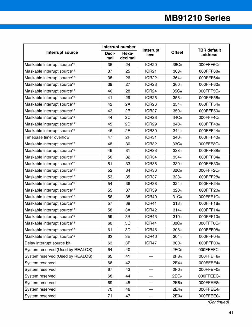
Maskable interrupt source*2 36 24 ICR20 36CH 000FFF6CH
Maskable interrupt source*2 37 25 ICR21 368H 000FFF68H
Maskable interrupt source*2 38 26 ICR22 364H 000FFF64H
Maskable interrupt source*2 39 27 ICR23 360H 000FFF60H
Maskable interrupt source*2 40 28 ICR24 35CH 000FFF5CH
Maskable interrupt source*2 41 29 ICR25 358H 000FFF58H
Maskable interrupt source*2 42 2A ICR26 354H 000FFF54H
Maskable interrupt source*2 43 2B ICR27 350H 000FFF50H
Maskable interrupt source*2 44 2C ICR28 34CH 000FFF4CH
Maskable interrupt source*2 45 2D ICR29 348H 000FFF48H
Maskable interrupt source*2 46 2E ICR30 344H 000FFF44H
Timebase timer overflow 47 2F ICR31 340H 000FFF40H
Maskable interrupt source*2 48 30 ICR32 33CH 000FFF3CH
Maskable interrupt source*2 49 31 ICR33 338H 000FFF38H
Maskable interrupt source*2 50 32 ICR34 334H 000FFF34H
Maskable interrupt source*2 51 33 ICR35 330H 000FFF30H
Maskable interrupt source*2 52 34 ICR36 32CH 000FFF2CH
Maskable interrupt source*2 53 35 ICR37 328H 000FFF28H
Maskable interrupt source*2 54 36 ICR38 324H 000FFF24H
Maskable interrupt source*2 55 37 ICR39 320H 000FFF20H
Maskable interrupt source*2 56 38 ICR40 31CH 000FFF1CH
Maskable interrupt source*2 57 39 ICR41 318H 000FFF18H
Maskable interrupt source*2 58 3A ICR42 314H 000FFF14H
Maskable interrupt source*2 59 3B ICR43 310H 000FFF10H
Maskable interrupt source*2 60 3C ICR44 30CH 000FFF0CH
Maskable interrupt source*2 61 3D ICR45 308H 000FFF08H
Maskable interrupt source*2 62 3E ICR46 304H 000FFF04H
Delay interrupt source bit 63 3F ICR47 300H 000FFF00H
System reserved (Used by REALOS) 64 40 — 2FCH 000FFEFCH
System reserved (Used by REALOS) 65 41 — 2F8H 000FFEF8H
System reserved 66 42 — 2F4H 000FFEF4H
System reserved 67 43 — 2F0H 000FFEF0H
System reserved 68 44 — 2ECH 000FFEECH
System reserved 69 45 — 2E8H 000FFEE8H
System reserved 70 46 — 2E4H 000FFEE4H
System reserved 71 47 — 2E0H 000FFEE0H
41

MB91210 Series
42
(Continued)
*1: Even though the TBR value is changed, fixed addresses, 000FFFFCH and 000FFFF8H, are always used for the reset vector and the mode vector.
*2: The maskable interrupt source is defined for each model.
Interrupt sourceInterrupt number
Interrupt level Offset TBR default
addressDeci-mal
Hexa-decimal
System reserved 72 48 — 2DCH 000FFEDCH
System reserved 73 49 — 2D8H 000FFED8H
System reserved 74 4A — 2D4H 000FFED4H
System reserved 75 4B — 2D0H 000FFED0H
System reserved 76 4C — 2CCH 000FFECCH
System reserved 77 4D — 2C8H 000FFEC8H
System reserved 78 4E — 2C4H 000FFEC4H
System reserved 79 4F — 2C0H 000FFEC0H
Used in INT instruction80 to
255
50 to FF
—2BCH
to 000H
000FFEBCH
to 000FFC00H

MB91210 Series
PIN STATUS IN EACH CPU STATETerms used as the status of pins mean as follows.
• Input enabledIndicates that the input function can be used.
• Output Hi-ZMeans the placing of a pin in a high impedance state by preventing the transistor for driving the pin from driving.
• Output maintainedIndicates the output in the output state existing immediately before this mode is established. If the deviceenters this mode with an internal output peripheral operating or while serving as an output port, the output isperformed by the internal peripheral or the port output is maintained, respectively.
• State existing immediately before is maintained.When the device serves for output or input immediately before entering this mode, the device maintains theoutput or is ready for the input, respectively.
43

MB91210 Series
44
TABLE OF PIN STATUS IN EACH MODE• Single chip mode
(Continued)
Pin name Function nameInitial value
In sleep stateIn stop state
INITX = “L” INITX = “H” HIZ = 0 HIZ = 1
INITX INITX
Input enabled
Input enabled
Input enabled
Input enabled Input enabled
X0 X0Hi-Z or input
enabledHi-Z or input
enabled
X1 X1”H” output or input enabled
”H” output or input enabled
X0A X0AHi-Z or input
enabledHi-Z or input
enabled
X1A X1A”H” output or input enabled
”H” output or input enabled
MD0 MD0
Input enabled Input enabledMD1 MD1
MD2 MD2
MD3 MD3
P00 P00/SIN5/INT8R
Output Hi-Z input enabled
Output Hi-Z input enabled
P : Immediately preceding status heldF : Normal operation performed
P : Immediately preceding status heldF : Output held or Hi-Z , input enabled
Output Hi-Z/selecting interrupt function, and input enabled when interrupt is allowed during ENIRinternal input held
P01 P01/SOT5/INT9R
P02 P02/SCK5/INT10R
P03 P03/SIN6/INT11R
P04 P04/SOT6/INT12R
P05 P05/SCK6/INT13R
P06 P06/OUT4/INT14R
P07 P07/OUT5/INT15R
P10 P10/TIN1
Output Hi-Zinternal input held
P11 P11/TOT1
P12 P12/SIN3
P13 P13/SOT3
P14 P14/SCK3
P15 P15/SIN4
P16 P16/SOT4
P17 P17/SCK4
P20 to P27P20 to P27/
PPG0, 2, 4, 6, 8, A, C, E

MB91210 Series
(Continued)
Pin name Function nameInitial value
In sleep stateIn stop state
INITX = “L” INITX = “H” HIZ = 0 HIZ = 1
P30P30/ (RX2) /
(INT10C)
Output Hi-Z input enabled
Output Hi-Z input enabled
P : Immediately preceding status heldF : Normal operation performed
P : Immediately preceding status heldF : Output held or Hi-Z , input enabled
Output Hi-Z/selecting interrupt function, and input enabled when interrupt is allowed during ENIRinternal input held
P31 P31/ (TX2) Output Hi-Zinternal input held
P32 P32/INT10 Output Hi-Z/selecting interrupt function, and input enabled when interrupt is allowed during ENIRinternal input held
P33 to P37P33 to P37/
INT11 to INT15
P40 to P43P40 to P43/
PPG9, B, D, F
Output Hi-Zinternal input held
P44 to P47P44 to P47/IN0 to IN3
P50 to P53P50 to P53/
PPG1, 3, 5, 7
P54 P54/IN4
P55 P55/IN5
P56 P56/IN6
P57 P57/IN7
P60 P60/OUT6
P61 P61/OUT7
P62 P62
P63 P63
P64 P64
P70 P70/RX0/INT8
Output Hi-Z/selecting interrupt function, and input enabled when interrupt is allowed during ENIRinternal input held
P71 P71/TX0Output Hi-Zinternal input held
45

MB91210 Series
46
(Continued)
Pin name Function nameInitial value
In sleep stateIn stop state
INITX = “L” INITX = “H” HIZ = 0 HIZ = 1
P72 P72/RX1/INT9
Output Hi-Z input enabled
Output Hi-Z input enabled
P : Immediately preceding status heldF : Normal operation performed
P : Immediately preceding status heldF : Output held or Hi-Z , input enabled
Output Hi-Z/selecting interrupt function, and input enabled when interrupt is allowed during ENIRinternal input held
P73 P73/TX1
Output Hi-Zinternal input held
P74 to P77P74 to P77/
OUT0 to OUT3
P80 to P83P80 to P83/
FRCK0 to FRCK3
P84 P84/TIN2
P85 P85/TOT2
P90 to P97P90 to P97/PPG0R, 2R, ER/AN0 to AN7
Output Hi-Zinternal input held
PA0 PA0/SIN2R/AN8
PA1 PA1/SOT2R/AN9
PA2 PA2/SCK2R/AN10
PA3 to PA7
PA3 to PA7/AN11 to AN15
PB0 to PB7
PB0 to PB7/INT0R to INT7R/AN16 to AN23
Output Hi-Z/selecting interrupt function, and input enabled when interrupt is allowed during ENIRinternal input held
PC0 to PC7
PC0 to PC7/AN24 to AN31
Output Hi-Zinternal input held

MB91210 Series
(Continued)
Pin name Function nameInitial value
In sleep stateIn stop state
INITX = “L” INITX = “H” HIZ = 0 HIZ = 1
PD0 PD0/TIN0/ATGX
Output Hi-Z input enabled
Output Hi-Z input enabled
P : Immediately preceding status heldF : Normal operation performed
P : Immediately preceding status heldF : Output held or Hi-Z , input enabled
Output Hi-Zinternal input held
PD1 PD1/TOT0
PD2 PD2/SIN0
PD3 PD3/SOT0
PD4 PD4/SCK0
PD5 PD5/SIN1
PD6 PD6/SOT1
PD7 PD7/SCK1
PE0 PE0/SIN2
PE1 PE1/SOT2
PE2 PE2/SCK2
PF0 to PF7PF0 to PF7/INT0 to INT7
Output Hi-Z/selecting interrupt function, and input enabled when interrupt is allowed during ENIRinternal input held
47

MB91210 Series
48
ELECTRICAL CHARACTERISTICS1. Absolute Maximum Ratings
*1: Caution must be taken that AVCC does not exceed VCC upon power-on and under other circumstances.
*2: The maximum output current defines the peak current value of each of the corresponding pins.
*3: The average output current defines the average value of the current (100 ms) which passes through each of the corresponding pins. The average value represents a value calculated by multiplying the operating current by the operating rate.
*4: The total average output current defines the average value of the current (100 ms) which passes through all the corresponding pins. The average value represents a value calculated by multiplying the operating current by the operating rate.
*5: • Corresponding pins : P00 to P07, P10 to P17, P20 to P27, P30 to P37, P40 to P47, P50 to P57, P60 to P64,P70 to P77, P80 to P85, P90 to P97, PA0 to PA7, PB0 to PB7, PC0 to PC7, PD0 to PD7,PE0 to PE2,PF0 to PF7
• Use within recommended operating conditions. • Use at DC voltage (current).• The + B signal should always be applied a limiting resistor placed between the + B signal and the
microcontroller.• The value of the limiting resistor should be set so that when the + B signal is applied the input current to
the microcontroller pin does not exceed rated values, either instantaneously or for prolonged periods.• Note that, when the microcontroller drive current is low as in low power consumption mode, the + B input
potential can increase the potential at the VCC pin via a protection diode, possibly affecting other devices.(Continued)
Parameter SymbolRating
Unit RemarksMin Max
Power supply voltage
VCC VSS − 0.3 VSS + 6.0 V
AVCC VSS − 0.3 VSS + 6.0 V AVCC = VCC*1
AVRH VSS − 0.3 VSS + 6.0 V AVCC ≥ AVRH
Input voltage VI VSS − 0.3 VCC + 0.3 V
Output voltage VO VSS − 0.3 VCC + 0.3 V
Maximum clamp current ICLAMP − 2.0 + 2.0 mA *5
Total maximum clamp current ΣICLAMP — 20 mA *5
“L” level maximum output current*2 IOL1 — 8 mA
“L” level average output current*3 IOLAV1 — 2 mA
“L” level total maximum output current ΣIOL1 — 64 mA
“L” level total average output current*4 ΣIOLAV1 — 25 mA
“H” level maximum output current*2 IOH1 — − 8 mA
“H” level average output current*3 IOHAV1 — − 2 mA
“H” level total maximum output current ΣIOH1 — − 64 mA
“H” level total average output current*4 ΣIOHAV1 — − 25 mA
Power consumption PD — 500 mW
Operating temperature TA − 40 + 105 °C Single-chip mode
Storage temperature Tstg − 55 + 150 °C

MB91210 Series
(Continued)• Note that, if the + B input exists when the microcontroller is off (not fixed at 0 V), power is supplied through
the pin, possibly causing the microcontroller to operate imperfectly.Note that, if the + B input exists when the power supply is turned on, power is supplied through the pin, possibly resulting in a power-supply voltage at which a power-on reset does not work.
• Be careful not to let the + B input pin open.• Note that the analog I/O pins (such as the LCD drive and comparator input pins) other than the A/D input
pin cannot input + B.• Recommended example circuit
WARNING: Semiconductor devices can be permanently damaged by application of stress (voltage, current, temperature, etc.) in excess of absolute maximum ratings. Do not exceed these ratings.
P-ch
N-ch
VCC
R
• Input/output equivalent circuits
+ B Input (0 V to 16 V)
Limiting resistor
Protection diode
49

MB91210 Series
50
2. Recommended operation condition(VSS=AVSS=0.0 V)
* : For how to connect the smoothing capacitor CS, see the figure below.
• C Pin Connection Diagram
WARNING: The recommended operating conditions are required in order to ensure the normal operation of thesemiconductor device. All of the device’s electrical characteristics are warranted when the device isoperated within these ranges.
Always use semiconductor devices within their recommended operating condition ranges. Operationoutside these ranges may adversely affect reliability and could result in device failure.No warranty is made with respect to uses, operating conditions, or combinations not represented onthe data sheet. Users considering application outside the listed conditions are advised to contact theirFUJITSU representatives beforehand.
Parameter SymbolValue
Unit RemarksMin Max
Power supply voltage
VCC
AVCC3.5 5.5 V Normal operation
VCC 3.0 5.5 V RAM data retention at STOP operation
Smoothing capacitor* CS1
(within tolerance ± 50%)µF
Use a ceramic capacitor or a capacitor with similar frequency characteristics.Use a bypass capacitor for the VCC pin, which has larger than CS.
Operating temperature TA − 40 + 105 °C Single-chip mode
CS
C
VSS AVSS

MB91210 Series
3. DC Specifications(TA: Recommended operating conditions; VCC = 5.0 V ±10%, VSS = AVSS = 0.0 V)
*1 : CLKB = 40 MHz, CLKP = 20 MHz, CLKT = 10 MHz, CANCLK = 10 MHz
*2 : Under *2, CPU stopped.
*3 : CLKB = CLKP = CLKT = CANCLK = 32 kHz, TA = + 25 °C
*4 : CPU/peripheral circuit operation stopped, main oscillation stopped, 32 kHz clock operation, TA = + 25 °C
*5 : CPU/peripheral circuit operation stopped, sub-oscillation stopped, 4 kHz clock operation, TA = + 25 °C
*6 : CPU/peripheral circuit operation stopped, all oscillation circuits stopped, TA = + 25 °C
*7 : The current consumption in normal operation/SLEEP mode, is the value at the maximum operation of the peripheral circuit.
Parameter Symbol Pin name Condition
ValueUnit Remarks
Min Typ Max
“H” level input voltage
VIHS — — 0.8 × VCC — VCC + 0.3 V CMOS automotive input
VIHC — — 0.7 × VCC — VCC + 0.3 V CMOS Schmitt input
VIHM
MD0 to
MD3— VCC − 0.3 — VCC + 0.3 V
VIHI INITX — 0.8 × VCC — VCC + 0.3 V
“L” level input voltage
VILS — — VSS − 0.3 — 0.5 × VCC V CMOS automotive input
VILC — — VSS − 0.3 — 0.3 × VCC V CMOS Schmitt input
VILM
MD0 to
MD3— VSS − 0.3 — VSS + 0.3 V
VILI INITX — VSS − 0.3 — 0.2 × VCC V
Power supply current
ICC VCC
*1 — 40 60 mA Normal operation *7
⎯ — 2 3 mAPLL stop operation (2 MHz)
ICCS VCC *2 — 28 42 mA SLEEP operation *7
ICCL VCC *3 — 150 300 µA Sub-operation *7
ICCR32 VCC *4 — 80 200 µA 32 kHz clock operation
ICCR4 VCC *5 — 800 1200 µA 4 MHz clock operation
ICCH VCC *6 — 70 150 µA STOP
Input leakage current
IIL — ⎯ − 5 — + 5 µA All input pins
Input capacity CIN — ⎯ — 5 15 pF
Pull-up resistance
RUP — ⎯ 25 50 100 kΩ All ports and INITX
Pull-down resistance
RDOWN — ⎯ 25 50 100 kΩ Exclusive of all Flash memory product
Output H voltage VOH ⎯ IOH= − 2 mA VCC − 0.5 — — V All ports
Output L voltage VOL ⎯ IOL=2 mA — — 0.4 V All ports
51

MB91210 Series
52
4. AC Specifications(1) Clock timing
(TA: Recommended operating conditions; VCC = 5.0 V ±10%, VSS = AVSS = 0.0 V)
Parameter Symbol Pin name ConditionValue
Unit RemarksMin Typ Max
Frequency of source oscillation clock
FC X0, X1
—
— 4 16 MHz
FCA X0A, X1A— 32.768 100 kHz MB91F213
— 32.768 — kHz MB91F211
Source oscillation clock cycle time
tCYL X0, X1 62.5 250 — ns
tCYLL X0A, X1A 10 30.5 — µs
Input clock pulse width PWH, PWL X0 30 — — nsThe duty ration normally ranges from 40% to 60%.
Input clock rise/fall time
tcr, tcf X0 — — 5 nsWhen external clock is used
Frequency of internal clock operation
FCP — — — 40 MHzWhen main clock and PLL clock is used.
Internal operation clock cycle time
tCP — — 25 — — nsWhen main clock and PLL clock is used.
tcr
0.2 Vcc 0.8 Vcc
PWL tcf
X0
PWH
tCYL

MB91210 Series
• Operation guarantee range
2 8 20 40
5.5
4.0
3.5
Relation between internal operation clock frequency and power supply voltage
Note : PLL operation stabilizing wait time should be set to 500 µs or more.
Relation between oscillation clock frequency and internal operation clock (example)
Source oscillation (4 MHz)
Divider 1/2 1/4 1/8
Multiplier FCP FCP FCP
1 – – –
2 – – 8 MHz
4 – 16 MHz 16 MHz
6 – 24 MHz –
8 32 MHz 32 MHz –
10 40 MHz – –
Source oscillation (5 MHz)
Divider 1/2 1/4 1/8
Multiplier FCP FCP FCP
1 – – –
2 – – 10 MHz
4 – 20 MHz –
6 – 30 MHz –
8 40 MHz – –
10 – – –
Source oscillation (10 MHz)
Divider 1/2 1/4 1/8
Multiplier FCP FCP FCP
1 – – 10 MHz
2 – 20 MHz –
4 40 MHz – –
6 – – –
8 – – –
10 – – –
Source oscillation (16 MHz)
Divider 1/2 1/4 1/8
Multiplier FCP FCP FCP
1 – 16 MHz 16 MHz
2 32 MHz 32 MHz –
4 – – –
6 – – –
8 – – –
10 – – –
–: Prohibited
Recommended operation range
PLL operationguarantee range
Pow
er s
uppl
y vo
ltage
VC
C (
V)
Internal operation clock FCP (MHz)
53

MB91210 Series
54
AC specifications are defined by the following measurement standard voltage values:
Input signal waveform Output signal waveform
Hysteresis input pin Output pin
Hysteresis input pin (Automotive)
0.3 Vcc 0.7 Vcc
0.4 V
4.6 V
0.5 Vcc 0.8 Vcc
C2C1
R
X0 X1
Example oscillation circuit

MB91210 Series
(2) Reset input(TA: Recommended operating conditions; VCC = 5.0 V ± 10%, VSS = AVSS = 0.0 V)
Parameter Symbol Pin name ConditionValue
Unit RemarksMin Max
INITX input time
tINTL INITX —
500 — ns
217 × tCYL — msUpon power-on and in stop mode
0.2 Vcc 0.2 Vcc
tINTL,
INITX
X0
tINTL
0.2 Vcc 0.2 VccINITX
• In stop mode
Oscillation time of oscillator
Oscillation stabilization wait time
90% of amplitude
Instruction executed
Internal operation
clock
Internal reset
55

MB91210 Series
56
[External reset input specifications (INITX) and internal reset signal cancellation timing]• When an external reset input is generated, a maximum of 256 tcp is designed to be spent until it reaches the
internal reset signal to transmit all reset signals to the internal logic.(Max 8 µs at 32 MHz)
• The following chart shows how to set the timing for instruction execution start (start of application operation)after external reset input.
Time from external reset input to instruction start = Max 256 tcp + 61 tcp
INITX
Max 256 tcp
Min
500 ns
61 tcp
• Timing Chart
Internal reset
Internal reset input timing
Internal reset cancellation timing

MB91210 Series
(3) Power-on Conditions(TA : Recommended operating conditions; VSS = 0.0 V)
(4) Power supply drop time, power supply voltages and external reset input to retain RAM data.
Satisfy the following reset input standard to retain the RAM data used in the single chip mode.
Parameter Symbol Pin name ConditionValue
Unit RemarksMin Max
Power supply rising time tR
VCC —
0.05 30 ms —
Power supply start voltage VOFF — 0.2 V —
Power supply peak voltage VON 3.5 — V —
Power supply cut-off time tOFF 50 — msDue to repetitive operation
VCC(V) Voltage drop time External reset input standard (INITX)
3.5 V → 3.0 V dropped Min 256 tcp Min 256 tcp
VCC 3.5 V 0.2 V 0.2 V 0.2 V
tR
tOFF
3.5 V
3.0 V 3.0 V
3.5 V
256 tcp
Vcc
INITX
To retain RAM data, enter 256 tcp of INITX or more before dropping VCC to 3.0 V or lower.
57

MB91210 Series
58
(5) UART Timing(TA: Recommended operating conditions; VCC = 5.0 V ± 10%, VSS = AVSS = 0.0 V)
Note: These are AC characteristics for CLK synchronous mode.CL is a load capacitance connected to pins during testing.
Parameter Symbol Pin name ConditionValue
Unit RemarksMin Max
Serial clock cycle time tSCYC SCK
Output pin, CL = 30 pF + 1 × TTL
8 tCP — ns
For internal shift clock mode
SCK ↓ → SOT delay time tSLOVSCKSOT
− 80 + 80 ns
Valid SIN → SCK ↑ tIVSHSCKSIN
100 — ns
SCK ↑ → Valid SIN hold time
tSHIX 60 — ns
Serial clock “H” pulse width
tSHSL
SCK
Output pin, CL = 30 pF + 1 × TTL
4 tCP — ns
For external shift clock mode
Serial clock “L” pulse width tSLSH 4 tCP — ns
SCK ↓ → SOT delay time tSLOVSCKSOT
— 150 ns
Valid SIN → SCK ↑ tIVSHSCKSIN
60 — ns
SCK ↑ → Valid SIN hold time
tSHIX 60 — ns

MB91210 Series
2.4 V
2.4 V 0.8 V
0.8 V
SIN
SOT
SCK
tSCYC
tSLOV
tSHIX tIVSH
0.7 VCC 0.3 VCC
0.7 VCC 0.3 VCC
0.8 V
• For internal shift clock mode
2.4 V
0.7 VCC 0.3 VCC
0.8 V
SIN
SOT
SCK
tSLSH
tSLOV
tSHIX tIVSH
0.7 VCC
0.3 VCC
0.7 VCC 0.3 VCC
0.7 VCC 0.3 VCC
tSHSL
• For external shift clock mode
59

MB91210 Series
60
(6) Timer Input Timing(TA: Recommended operating conditions; VCC = 5.0 V ± 10%, VSS = AVSS = 0.0 V)
(7) External Interrupt Timing(TA: Recommended operating conditions; VCC = 5.0 V ± 10%, VSS = AVSS = 0.0 V)
Parameter Symbol Pin name ConditionValue
UnitMin Max
Input pulse widthtTIWH
tTIWL
TIN0 to TIN2IN0 to IN7
— 4 tCP — ns
Parameter Symbol Pin name ConditionValue
UnitMin Max
Input pulse width tINTH, tINTL INT0 to INT15 ⎯ 3 tCP — ns
0.7 Vcc 0.3 Vcc
TINx INx
tTIWL tTIWH
0.7 Vcc 0.3 Vcc
• Timer Input Timing
0.8 VCC 0.5 VCCINTx
tINTL tINTH
0.8 VCC 0.5 VCC
• External Interrupt Input Timing

MB91210 Series
5. Flash Memory Write/Erase Characteristics
*: This value comes from the technology qualification (using Arrhenius equation to translate high temperature measurements into normalized value at + 85 °C).
Parameter ConditionValue
Unit RemarksMin Typ Max
Sector erase timeTA= + 25 °C, VCC=5.0 V
— 0.5 2.0 sExclusive of internal write time prior to erase
Word write timeTA= + 25 °C VCC=5.0 V
— 6 100 µsExclusive of overhead time at system level
Chip write timeTA= + 25 °C, VCC=5.0 V
— 3.4 56 sExclusive of overhead time at system level
Erase/write cycle ⎯ 10000 — — cycle
Data retention time Average TA= + 85 °C 20* — — year
61

MB91210 Series
62
6. A/D Converter Electrical Characteristics(TA : Recommended operating conditions; VCC = 3.5 V to 5.5 V, VSS = AVSS = 0.0 V)
*1 : When FCP is 40 MHz : tSMP = (Rext + Rin) × Cin × 7 = ST × CLKP cycle = 2 Ah × 25 ns = 1.1 µs
*2 : When FCP is 40 MHz : tCMP = CKIN × 11 = CT × CLKP cycle × 11 = 4 h × 25 ns × 11 = 1.1 µs
*3 : This represents the conversion time per channel when tSMP and tCMP are selected while FCP is 40 MHz.(Continued)
Parameter Symbol Pin nameValue
Unit RemarksMin Typ Max
Resolution — — — — 10 bit
Total error — — — — ± 3.0 LSB
Non-liner error — — — — ± 2.5 LSB
Differential linearity error
— — — — ± 1.9 LSB
Zero transition voltage VOT AN0 to AN31AVSS − 1.5LSB
AVSS + 0.5LSB
AVSS + 2.5LSB
V1LSB = (AVRH-AVSS)/1024Full-scale transition
voltageVFST AN0 to AN31
AVRH − 3.5LSB
AVRH − 1.5LSB
AVRH + 0.5LSB
V
Sampling time tSMP —
1.1 — — µsVCC = AVCC = 4.5 V to 5.5 V*1
1.65 ⎯ ⎯ µsVCC = AVCC = 3.5 V to 4.5 V*5
Compare time tCMP —
1.1 — — µsVCC = AVCC = 4.5 V to 5.5 V*2
2.2 ⎯ ⎯ µsVCC = AVCC = 3.5 V to 4.5 V*6
A/D conversion time tCNV —
2.2 — — µsVCC = AVCC = 4.5 V to 5.5 V*3
3.85 ⎯ ⎯ µsVCC = AVCC = 3.5 V to 4.5 V*7
Analog port input current
IAIN AN0 to AN31 — — 10 µA VAVSS ≤ VAIN ≤ VAVCC
Analog input voltage VAIN AN0 to AN31 0 — AVRH V
Standard voltage AVRH AVRH 4.0 — AVCC V
Power supply currentIA
AVCC— 2.4 4.7 mA
IAH — — 5 µA *4
Standard voltage supply current
IR
AVRH— 600 900 µA VAVRH = 5.0 V
IRH — — 5 µA *4
Variation between channels
— AN0 to AN31 — — 4 LSB

MB91210 Series
(Continued)
*4: This defines the power supply current when the A/D converter is not in operation and the CPU is stopped (at “VCC = AVCC = AVRH = 5.0 V”)
*5 : When FCP is 20 MHz : tSMP = (Rext + Rin) × Cin × 7 = ST × CLKP cycle = 21h × 50 ns = 1.65 µs.
*6 : When FCP is 20 MHz : tCMP = CKIN × 11 = CT × CLKP cycle × 11 = 4 h × 50 ns × 11 = 2.2 µs.
*7 : This represents the conversion time per channel when tSMP and tCMP are selected while FCP is 20 MHz.
• Analog Input Equivalent Circuit
Notes: • As AVRH becomes smaller, the error becomes greater.• Use the output impedance rS of the external circuit for analog input under the following conditions :
Output impedance rS of the external circuit = 4 kΩ (Max)• If the output impedance of the external circuit is too high, the sampling time of the analog voltage may
not be sufficient.• When placing a DC blocking capacitor between the external circuit and input pin, set the capacitance to
the value calculated by multiplying CSH by several thousands as a guideline in order to minimize the impact from dividing voltage capacitance with CSH.
CSH
VS
rS RSH
<Recommended parameter values and tentative guideline for each element>rS 4 kΩ or lessRSH = approx. 2.5 kΩ (5 V ± 10%) CSH = approx. 8.5 pFNote: These element parameters should be regarded as tentative values used only for design purposes.
Input pin AN0
Circuit in microcontroller
Input pin AN7
Analog channel selector
S/H circuit
Comparator
63

MB91210 Series
64
TERM DEFINITIONSResolution
Level of analog variation that can be distinguished by the A/D converter.When the number of bits is 10, the analog voltage can be resolved into 210 = 1024.
Total errorDifference between actual and theoretical values, which is a total value derived from an offset error, gain error,non-linearity error and noise.
Linearity errorDeviation between the value along a straight line connecting the zero transition point (“00 0000 0000” ←→ “00 0000 0001”) of a device and the full-scale transition point (“11 1111 1110” ←→ “11 1111 1111”) compared with the actual conversion values obtained.
Differential linearity errorDeviation of input voltage, which is required for changing output code by 1 LSB, from an ideal value.
00 0000 0000 VFST V0T V (N+1)T VNT
1LSB × N + V0T
00 0000 0001 00 0000 0010 00 0000 0011
11 1111 1100 11 1111 1101 11 1111 1110 11 1111 1111
N = A/D converter digital output value.V0T = AVss + 0.5LSB [V] (Theoretical value)VFST = AVRH 1.5LSB [V] (Theoretical value)VNT: Transition voltage of digital output from N-1 to N
Linearity error=VNT − (1LSB × N + VOT)
[LSB]1LSB
Differential linearity error=V(N + 1)T − VNT
− 1 [LSB]1LSB
• 10-bit A/D Converter- Conversion Characteristics

MB91210 Series
ORDERING INFORMATION
Part No. Package
MB91F211PMC-GSE1100-pin plastic LQFP
(FPT-100P-M20)
MB91213PMC-GSE1144-pin plastic LQFP
(FPT-144P-M08)
MB91F213PMC-GSE1144-pin plastic LQFP
(FPT-144P-M08)
MB91V210PB-ESE1420-pin plastic PBGA
(BGA-420P-M01)
65

MB91210 Series
66
PACKAGE DIMENSION
Please confirm the latest Package dimension by following URL.http://edevice.fujitsu.com/fj/DATASHEET/ef-ovpklv.htmll
(Continued)
100-pin plastic LQFP Lead pitch 0.50 mm
Package width ×package length
14.0 mm × 14.0 mm
Lead shape Gullwing
Sealing method Plastic mold
Mounting height 1.70 mm Max
Weight 0.65 g
Code(Reference)
P-LFQFP100-14×14-0.50
100-pin plastic LQFP(FPT-100P-M20)
(FPT-100P-M20)
C 2005 FUJITSU LIMITED F100031S-c-2-1
14.00±0.10(.551±.004)SQ
16.00±0.20(.630±.008)SQ
1 25
26
51
76 50
75
100
0.50(.020) 0.20±0.05(.008±.002)
M0.08(.003)0.145±0.055
(.0057±.0022)
0.08(.003)
"A"
INDEX.059 –.004
+.008–0.10+0.20
1.50(Mounting height)
0˚~8˚
(0.50(.020))
(.024±.006)0.60±0.15
0.25(.010)
0.10±0.10(.004±.004)
Details of "A" part
(Stand off)
*
Dimensions in mm (inches).Note: The values in parentheses are reference values
Note 1) * : These dimensions do not include resin protrusion.Note 2) Pins width and pins thickness include plating thickness.Note 3) Pins width do not include tie bar cutting remainder.

MB91210 Series
(Continued)
Please confirm the latest Package dimension by following URL.http://edevice.fujitsu.com/fj/DATASHEET/ef-ovpklv.html
144-pin plastic LQFP Lead pitch 0.50 mm
Package width ×package length
20.0 × 20.0 mm
Lead shape Gullwing
Sealing method Plastic mold
Mounting height 1.70 mm MAX
Weight 1.20g
Code(Reference)
P-LFQFP144-20×20-0.50
144-pin plastic LQFP(FPT-144P-M08)
(FPT-144P-M08)
C 2003 FUJITSU LIMITED F144019S-c-4-6
Details of "A" part
0.25(.010)
(Stand off)(.004±.004)0.10±0.10
(.024±.006)0.60±0.15
(.020±.008)0.50±0.20
1.50+0.20–0.10
+.008–.004.059
0˚~8˚
0.50(.020)
"A"
0.08(.003)
0.145±0.055(.006±.002)
LEAD No. 1 36
INDEX
37
72
73108
109
144
0.22±0.05(.009±.002)
M0.08(.003)
20.00±0.10(.787±.004)SQ
22.00±0.20(.866±.008)SQ
(Mounting height)
*
Dimensions in mm (inches).Note: The values in parentheses are reference values.
Note 1) *:Values do not include resin protrusion.Resin protrusion is +0.25(.010)Max(each side).
Note 2) Pins width and pins thickness include plating thickness.Note 3) Pins width do not include tie bar cutting remainder.
67

MB91210 Series
F0702
The information for microcontroller supports is shown in the following homepage.http://www.fujitsu.com/global/services/microelectronics/product/micom/support/index.html
FUJITSU LIMITEDAll Rights Reserved.
The contents of this document are subject to change without notice. Customers are advised to consult with FUJITSU salesrepresentatives before ordering.The information, such as descriptions of function and applicationcircuit examples, in this document are presented solely for thepurpose of reference to show examples of operations and uses ofFujitsu semiconductor device; Fujitsu does not warrant properoperation of the device with respect to use based on suchinformation. When you develop equipment incorporating thedevice based on such information, you must assume anyresponsibility arising out of such use of the information. Fujitsuassumes no liability for any damages whatsoever arising out ofthe use of the information.Any information in this document, including descriptions offunction and schematic diagrams, shall not be construed as licenseof the use or exercise of any intellectual property right, such aspatent right or copyright, or any other right of Fujitsu or any thirdparty or does Fujitsu warrant non-infringement of any third-party’sintellectual property right or other right by using such information.Fujitsu assumes no liability for any infringement of the intellectualproperty rights or other rights of third parties which would resultfrom the use of information contained herein.The products described in this document are designed, developedand manufactured as contemplated for general use, includingwithout limitation, ordinary industrial use, general office use,personal use, and household use, but are not designed, developedand manufactured as contemplated (1) for use accompanying fatalrisks or dangers that, unless extremely high safety is secured, couldhave a serious effect to the public, and could lead directly to death,personal injury, severe physical damage or other loss (i.e., nuclearreaction control in nuclear facility, aircraft flight control, air trafficcontrol, mass transport control, medical life support system, missilelaunch control in weapon system), or (2) for use requiringextremely high reliability (i.e., submersible repeater and artificialsatellite).Please note that Fujitsu will not be liable against you and/or anythird party for any claims or damages arising in connection withabove-mentioned uses of the products.Any semiconductor devices have an inherent chance of failure. Youmust protect against injury, damage or loss from such failures byincorporating safety design measures into your facility andequipment such as redundancy, fire protection, and prevention ofover-current levels and other abnormal operating conditions.If any products described in this document represent goods ortechnologies subject to certain restrictions on export under theForeign Exchange and Foreign Trade Law of Japan, the priorauthorization by Japanese government will be required for exportof those products from Japan.The company names and brand names herein are the trademarks orregistered trademarks of their respective owners.
Edited Business Promotion Dept.