fpga laboratory assignment 1 due date: 2/10/2018 · a vhdl module should now appear in project...
TRANSCRIPT

Department of Electrical and Computer Engineering, University of Cyprus
FPGA Laboratory Assignment 1
Due Date: 2/10/2018
Aim The purpose of this lab is to introduce you to the basic FPGA design and
programming tools. For the purposes of this lab you will first perform an installation
of the tools and then implement an adder circuit using FPGA design flow.
Objectives
• Verify that the Xilinx tools are up and running
• Introduce you to the Xilinx Vivado ISE software.
• Become familiar with VHDL/Verilog coding and use of the simulator (ISim).
• Be able to synthesize and implement designs to FPGAs using ISE.
Equipment & Tools Xilinx Vivado Suite
You can visit http://www.xilinx.com/products/design-tools/vivado.html
and choose the version you want. For this tutorial we use an older version but the
board is fully compatible with latest versions. You can download the ISE Webpack
for free, but if you have trouble installing it, let me know ASAP.
ISE Simulator (Isim)
Introduction This is a step-by-step tutorial for building a 1-bit full adder and a D flip-flop in Xilinx
Vivado, a Design Suite software that provides designers with the ability to code
designs in a hardware description language such as VHDL or Verilog. The ISE
Design Suite also provides the ability to apply FPGA pin and timing constraints,
analyse for errors and violations, and synthesize to generate configuration bit file
formats for FPGAs.
ECE408 -Digital Design with FPGAs 1
Department of Electrical and Computer Engineering, University of Cyprus
By the end of this tutorial, you should be able to:
• Create a new design by VHDL coding.
• Verify the function of a design by behavioural simulation.
• Map a design to an FPGA device through placement and routing procedures.
• Estimate the performance of the design by timing analysis.
• Use the 1-bit full adder created in this tutorial to implement and simulate a 4-bit
adder.
Step-by-step 1-bit Full Adder Design
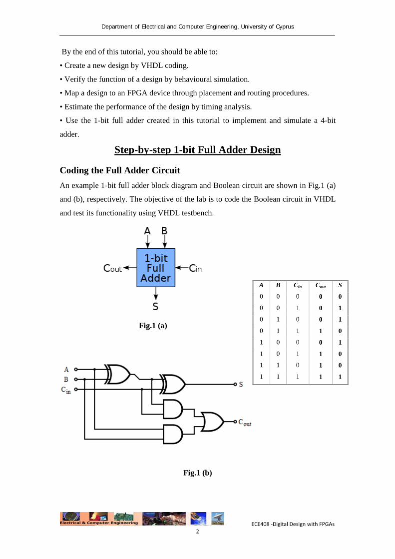
Coding the Full Adder Circuit An example 1-bit full adder block diagram and Boolean circuit are shown in Fig.1 (a)
and (b), respectively. The objective of the lab is to code the Boolean circuit in VHDL
and test its functionality using VHDL testbench.
Fig.1 (a)
Fig.1 (b)
A B Cin Cout S
0 0 0 0 0
0 0 1 0 1
0 1 0 0 1
0 1 1 1 0
1 0 0 0 1
1 0 1 1 0
1 1 0 1 0
1 1 1 1 1
ECE408 -Digital Design with FPGAs 2
Department of Electrical and Computer Engineering, University of Cyprus
Tasks:
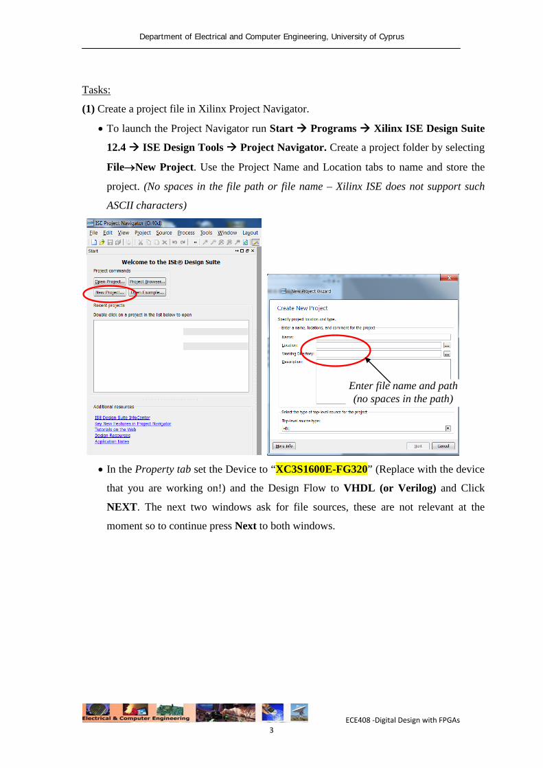
(1) Create a project file in Xilinx Project Navigator.
• To launch the Project Navigator run Start Programs Xilinx ISE Design Suite
12.4 ISE Design Tools Project Navigator. Create a project folder by selecting
File→New Project. Use the Project Name and Location tabs to name and store the
project. (No spaces in the file path or file name – Xilinx ISE does not support such
ASCII characters)
• In the Property tab set the Device to “XC3S1600E-FG320” (Replace with the device
that you are working on!) and the Design Flow to VHDL (or Verilog) and Click
NEXT. The next two windows ask for file sources, these are not relevant at the
moment so to continue press Next to both windows.
Enter file name and path (no spaces in the path)
ECE408 -Digital Design with FPGAs 3

Department of Electrical and Computer Engineering, University of Cyprus
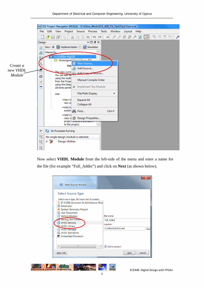
(2) Create a VHDL module.
• To create a VHDL module right-click on the icon xc3s1600e-4fg320 (shown
below) and select New Source.
Enter FPGA device
details and required simulator
ECE408 -Digital Design with FPGAs 4
Department of Electrical and Computer Engineering, University of Cyprus
Now select VHDL Module from the left-side of the menu and enter a name for
the file (for example “Full_Adder”) and click on Next (as shown below).
Create a new VHDL
Module
ECE408 -Digital Design with FPGAs 5

Department of Electrical and Computer Engineering, University of Cyprus
In the Architecture Name tab write “Behavioral” and enter the appropriate inputs and
outputs of the 1-bit Full Adder in the Port Name tab. Select Next and Finish to create
the VHDL module. (Click through the remaining menu to complete). Select
File→Save-all. (Remember to regularly save your work)
A VHDL module should now appear in project navigator, as shown below. This
provides the entity and architecture layout for your circuit.
(3) Edit the VHDL file to realise the 1-bit full-adder circuit depicted in Fig.1 (b). The
VHDL code is highlighted in the red box of Fig 2(a). When you have coded the circuit
in VHDL run the syntax checker: This is available in the process window under
Synthesize-XST → Check Syntax, see Fig. 2(b) below. When the design is error-
free, synthesize the VHDL file: Double click on Synthesize-XST.
Specify the signal
names and directions for the new
VHDL Module
ECE408 -Digital Design with FPGAs 6

Department of Electrical and Computer Engineering, University of Cyprus
Fig.2 (a)
Adder VHDL Code
ECE408 -Digital Design with FPGAs 7

Department of Electrical and Computer Engineering, University of Cyprus
Fig. 2 (b)
Synthesis Process
Synthesis report
ECE408 -Digital Design with FPGAs 8

Department of Electrical and Computer Engineering, University of Cyprus
Fig. 2 (c)
Now examine the synthesis report – this is available by right-clicking Synthesize-
XST and select View Text Report, see Fig. 2(b). Scroll down the file to find the
section entitled Final Report, as shown in Fig. 2(c). Note the number of LUTs and
IBUF/OBUFs that have been synthesised to create the circuit.
Behavioral Simulation of a Full Adder In this section, we will introduce the concept of test bench and show how to verify the
function of our full adder by behavioural simulation using the Xilinx Isim tool.
What is a test bench?
A test bench is an entity (usually a VHDL/Verilog program) which is used to verify
the correctness of a design. The design to be verified is called Unit Under Test (UUT).
The test bench supplies stimuli to the design, observes the outputs of the design, and
compares the observed outputs with the expected values. If any mismatch happens,
Synthesis report
ECE408 -Digital Design with FPGAs 9

Department of Electrical and Computer Engineering, University of Cyprus
the test bench issues certain messages signifying that there are errors in the design.
Fig. 3 shows the concept of test bench.
Fig.3: Conceptual Diagram of a test bench.
Advanced EDA tools such as Xilinx ISE usually have the capability to automatically
generate the test bench. All the users need to do is specifying the waveforms of the
stimuli and the expected outputs; the software produces the test bench program which
can be tailored later on.
Build the test bench by specifying waveforms
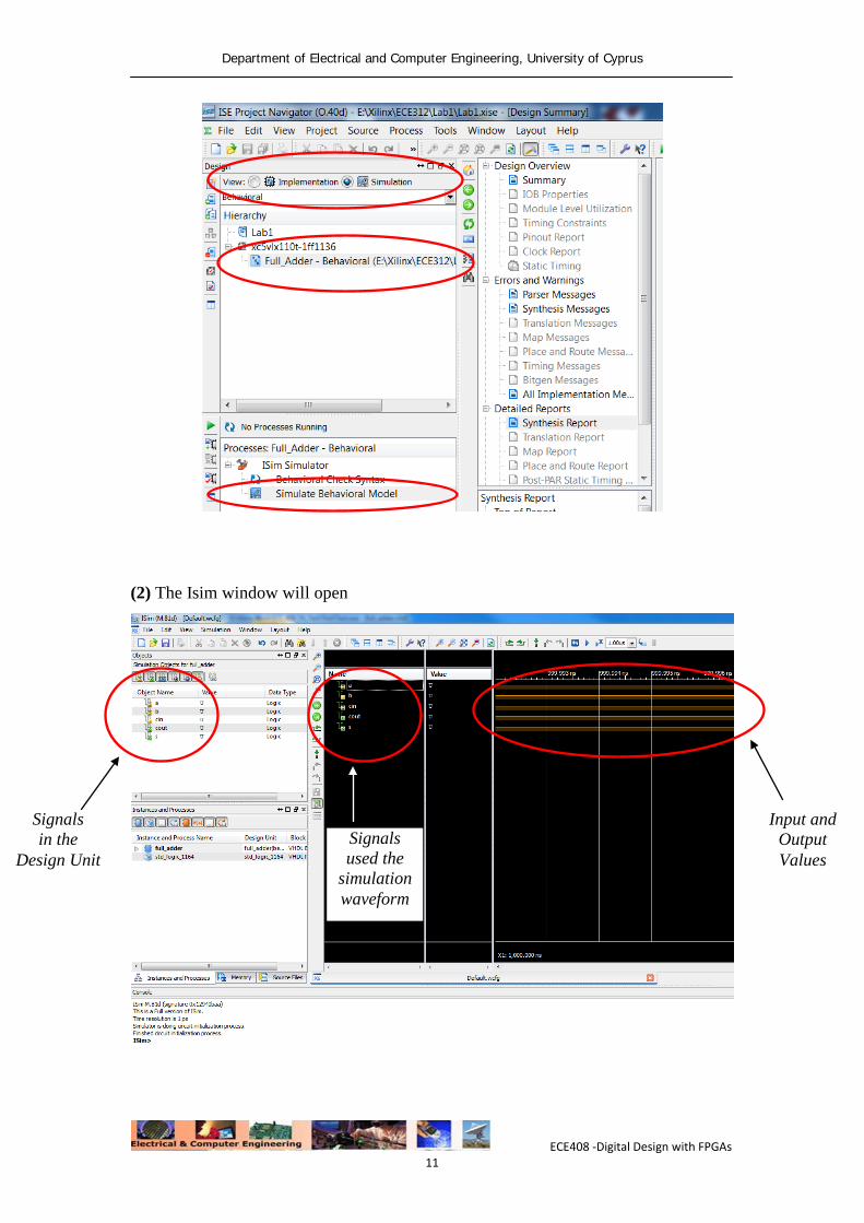
(1) In the Design Panel, select “Simulation”, click ‘Full_Adder - Behavioral’, and
then double-click ‘Simulate Behavioural Model’. You may need to hit the ‘+’ beside
‘ISim Simulator’.
ECE408 -Digital Design with FPGAs 10
Department of Electrical and Computer Engineering, University of Cyprus
(2) The Isim window will open
Signals in the
Design Unit Signals used the
simulation waveform
Input and Output Values
ECE408 -Digital Design with FPGAs 11

Department of Electrical and Computer Engineering, University of Cyprus
(3) You can rename the inputs/outputs by right-clicking them and hitting ‘rename’. If
you forget which ports are which, you can look back in ISE Project Navigator (not the
simulator). You can also right-click on a particular signal to initialize it to a constant
value, or define it as a clock.
Right click on a signal to initialize it to a constant value or set it as a clock
To initialize a signal select the desire radix and set the value
Select Radix
Enter Signal Value Here
ECE408 -Digital Design with FPGAs 12

Department of Electrical and Computer Engineering, University of Cyprus
To define a clock signal simple set the edge parameters and clock period.
(4) Using the waveform display, fill in the truth table. First, specify a running time
period, then enter the input values and press run. Do this until all the values have been
assigned. You may need to scroll the waveform to start at time 0. You can click on
different times in the waveform and just read S/Cout directly off. Fill in the
observations based on this.
Basic Simulation Controls. Keep in mind the clock period when defining the simulation run time
Select Time to run the simulation
e.g. 10ns
Run the simulation for the specified amount of time
Reset and Restart the simulation
Specify leading edge
value e.g. 1
Specify leading edge
value e.g. 0
Specify the period of the
clock e.g. 10ns
Zoom in and Out. View full waveform
ECE408 -Digital Design with FPGAs 13

Department of Electrical and Computer Engineering, University of Cyprus
(5) Close the ISim window, it will ask if you want to exit the application, hit “Yes”.
Build the test bench using VHDL coding
Another way to simulate the circuit to verify its expected Boolean behaviour is by
manually creating a Testbench for the circuit.
Tasks
(1) Right click on xc3s1600e-fg320 icon in the sources window and select New
Source, then select VHDL Test Bench and enter a filename and follow through to
finish
Create Testbench
ECE408 -Digital Design with FPGAs 14
Department of Electrical and Computer Engineering, University of Cyprus
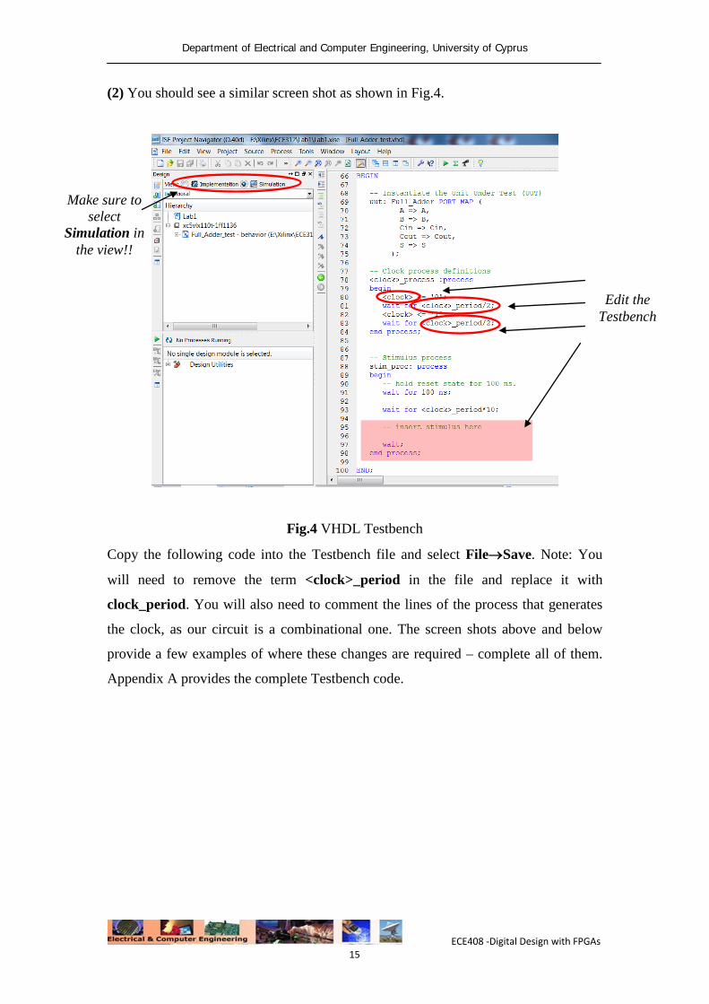
(2) You should see a similar screen shot as shown in Fig.4.
Fig.4 VHDL Testbench
Copy the following code into the Testbench file and select File→Save. Note: You
will need to remove the term <clock>_period in the file and replace it with
clock_period. You will also need to comment the lines of the process that generates
the clock, as our circuit is a combinational one. The screen shots above and below
provide a few examples of where these changes are required – complete all of them.
Appendix A provides the complete Testbench code.
Edit the Testbench
Make sure to select
Simulation in the view!!
ECE408 -Digital Design with FPGAs 15
Department of Electrical and Computer Engineering, University of Cyprus
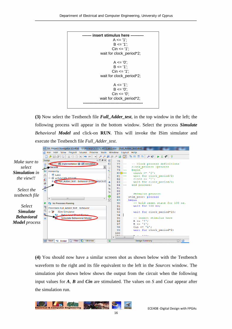
(3) Now select the Testbench file Full_Adder_test, in the top window in the left; the
following process will appear in the bottom window. Select the process Simulate
Behavioral Model and click-on RUN. This will invoke the ISim simulator and
execute the Testbench file Full_Adder_test.
(4) You should now have a similar screen shot as shown below with the Testbench
waveform to the right and its file equivalent to the left in the Sources window. The
simulation plot shown below shows the output from the circuit when the following
input values for A, B and Cin are stimulated. The values on S and Cout appear after
the simulation run.
------- insert stimulus here ---------- A <= '1'; B <= '1';
Cin <= '1'; wait for clock_period*2;
A <= '0'; B <= '1';
Cin <= '1'; wait for clock_period*2;
A <= '1'; B <= '0';
Cin <= '0'; wait for clock_period*2;
----------------------------------------------
Make sure to select
Simulation in the view!!
Select the testbench file
Select
Simulate Behavioral
Model process
ECE408 -Digital Design with FPGAs 16
Department of Electrical and Computer Engineering, University of Cyprus
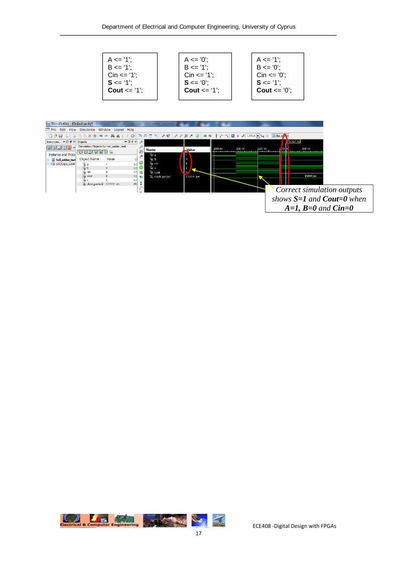
A <= '0'; B <= '1'; Cin <= '1'; S <= ‘0’; Cout <= ‘1’;
A <= '1'; B <= '1'; Cin <= '1'; S <= ‘1’; Cout <= ‘1’;
A <= '1'; B <= '0'; Cin <= '0'; S <= ‘1’; Cout <= ‘0’;
Correct simulation outputs shows S=1 and Cout=0 when
A=1, B=0 and Cin=0
ECE408 -Digital Design with FPGAs 17

Department of Electrical and Computer Engineering, University of Cyprus
Implement a 4-bit Adder Design The next step of this lab is to implement a 4-bit adder using the 1-bit full adder as the basic component. You should follow the process outlined for the 1-bit adder. Specifically, you are required to synthesize the 4-bit adder and simulate it either using a testbench or manually, to verify that it functions correctly.
• Synthesize the 4-bit adder design and report resource utilization from the synthesis text report. How does it compare to the 1-bit full adder?
Deliverables The ISE project folder containing the code and simulation files for both the 1-bit and 4-bit adders, and a lab report will be submitted electronically through email ([email protected]). Please use compression software to (winRar or 7zip) to keep the file size at a minimum. If the files are too large to be submitted via email please use the UCY file sending service https://filesender.ucy.ac.cy/filesender/.
• Please notify me in advance if you are going to delay delivering the lab
Also consider
• This lab briefly introduced you to the ISE design suite tools. You are advised to look at the tutorials posted on the lab web site for a more comprehensive overview and detailed explanation of the tools.
• You are encourage to visit the Xilinx user community forums (http://forums.xilinx.com/). The community forum enables Xilinx FPGA users to share, discuss, and resolve issues related to the Xilinx tools, HDL, FPGA programming and more.
GOOD LUCK
ECE408 -Digital Design with FPGAs 18

Department of Electrical and Computer Engineering, University of Cyprus
Appendix A The ISE® Language Templates provide predefined pieces of code and code syntax for use in your source files. These templates enable easy insertion of pre-built text structures into your VHDL, Verilog, Tcl, or UCF source file. There are several types of pre-built templates available, such as common language structures or instantiation templates for synthesis. To Use Language Templates:
1. Select Edit > Language Templates, or click the Language Templates toolbar button .
2. In the Language Templates window that opens in the Project Navigator Workspace, click the plus (+) icon next to one of the following folders: Tcl, UCF, VHDL, Verilog.
3. Click the plus (+) icon to expand the folders until you find the template you want to use.
4. Select the template to display it in the right pane. 5. Insert the code in your source file. Note that you will have to modify the port
names to that of your own source file.
VHDL Code
Examples
VHDL Code Examples
for Different
Components
Language toolbar button
ECE408 -Digital Design with FPGAs 19